ICGOO在线商城 > 分立半导体产品 > 晶体管 - FET,MOSFET - 单 > ZXMN6A11GTA
 Datasheet下载
- 型号: ZXMN6A11GTA
- 制造商: Diodes Inc.
- 库位|库存: xxxx|xxxx
- 要求:
| 数量阶梯 | 香港交货 | 国内含税 |
| +xxxx | $xxxx | ¥xxxx |
查看当月历史价格
查看今年历史价格
ZXMN6A11GTA产品简介:
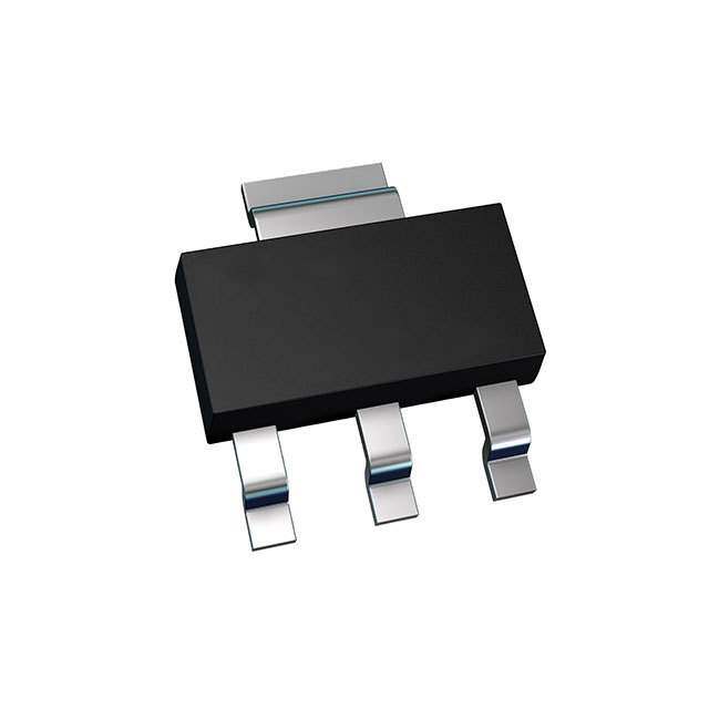
ICGOO电子元器件商城为您提供ZXMN6A11GTA由Diodes Inc.设计生产,在icgoo商城现货销售,并且可以通过原厂、代理商等渠道进行代购。 ZXMN6A11GTA价格参考。Diodes Inc.ZXMN6A11GTA封装/规格:晶体管 - FET,MOSFET - 单, 表面贴装 N 沟道 60V 3.1A(Ta) 2W(Ta) SOT-223。您可以下载ZXMN6A11GTA参考资料、Datasheet数据手册功能说明书,资料中有ZXMN6A11GTA 详细功能的应用电路图电压和使用方法及教程。
Diodes Incorporated生产的ZXMN6A11GTA是一款N沟道增强型MOSFET晶体管,适用于多种电子电路设计场景。以下是其主要应用场景:

 1. 电源管理
   - 开关电源(SMPS):ZXMN6A11GTA的低导通电阻(Rds(on))特性使其非常适合用作开关元件,用于提高效率和降低功耗。
   - DC-DC转换器:在降压或升压转换器中作为同步整流MOSFET,提供高效的电流切换。
   - 负载开关:用于控制电路中不同负载的开启与关闭,保护系统免受过流或短路的影响。

 2. 电机驱动
   - 小型直流电机控制:可用于驱动小型风扇、玩具电机或其他低功率直流电机,实现速度调节和方向控制。
   - H桥电路:在双向电机驱动应用中,该MOSFET可以用作H桥的一部分,支持正转和反转功能。

 3. 信号切换
   - 模拟信号切换:利用其低导通电阻和快速开关特性,在音频或视频信号路径中实现高效切换。
   - 数字信号隔离:在需要将一个电路与另一个电路电气隔离时,可用作信号缓冲或隔离器件。

 4. 保护电路
   - 过流保护:通过检测MOSFET的压降来监控电流,当电流超过设定值时切断电路。
   - 短路保护:结合控制器使用,快速响应并断开异常电流路径,防止设备损坏。
   - ESD保护:在敏感电路中,MOSFET可以用作输入/输出端口的保护元件。

 5. 消费类电子产品
   - 便携式设备:如移动电源、蓝牙音箱、智能手表等,ZXMN6A11GTA的小型封装(如SOT-23)适合紧凑型设计。
   - 电池管理系统(BMS):用于锂离子电池充电/放电保护电路,确保电池安全运行。

 6. 工业自动化
   - 传感器接口:用于工业传感器的信号放大或切换,支持远程数据采集。
   - 继电器替代:在低功率应用中,用MOSFET代替机械继电器以减少噪音并提高可靠性。

 总结
ZXMN6A11GTA凭借其优异的性能参数(如低Rds(on)、高开关速度和小封装尺寸),广泛应用于消费电子、工业控制、通信设备以及汽车电子等领域。它特别适合需要高效能、低功耗和小型化设计的应用场景。
| 参数 | 数值 |
| 产品目录 | |
| ChannelMode | Enhancement |
| 描述 | MOSFET N-CH 60V 3.1A SOT223MOSFET 60V N-Chnl UMOS |
| 产品分类 | FET - 单分离式半导体 |
| FET功能 | 逻辑电平门 |
| FET类型 | MOSFET N 通道,金属氧化物 |
| Id-ContinuousDrainCurrent | 4.4 A |
| Id-连续漏极电流 | 4.4 A |
| 品牌 | Diodes Incorporated |
| 产品手册 | |
| 产品图片 |
|
| rohs | 符合RoHS无铅 / 符合限制有害物质指令(RoHS)规范要求 |
| 产品系列 | 晶体管,MOSFET,Diodes Incorporated ZXMN6A11GTA- |
| 数据手册 | |
| 产品型号 | ZXMN6A11GTA |
| Pd-PowerDissipation | 3.9 W |
| Pd-功率耗散 | 3.9 W |
| RdsOn-Drain-SourceResistance | 180 mOhms |
| RdsOn-漏源导通电阻 | 180 mOhms |
| RoHS指令信息 | http://diodes.com/download/4349 |
| Vds-Drain-SourceBreakdownVoltage | 60 V |
| Vds-漏源极击穿电压 | 60 V |
| Vgs-Gate-SourceBreakdownVoltage | +/- 20 V |
| Vgs-栅源极击穿电压 | 20 V |
| 上升时间 | 3.5 ns |
| 下降时间 | 4.6 ns |
| 不同Id时的Vgs(th)(最大值) | 3V @ 250µA |
| 不同Vds时的输入电容(Ciss) | 330pF @ 40V |
| 不同Vgs时的栅极电荷(Qg) | 5.7nC @ 10V |
| 不同 Id、Vgs时的 RdsOn(最大值) | 120 毫欧 @ 2.5A,10V |
| 产品目录页面 | |
| 产品种类 | MOSFET |
| 供应商器件封装 | SOT-223 |
| 其它名称 | ZXMN6A11GTR |
| 其它图纸 |
|
| 典型关闭延迟时间 | 8.2 ns |
| 功率-最大值 | 2W |
| 包装 | 带卷 (TR) |
| 商标 | Diodes Incorporated |
| 安装类型 | 表面贴装 |
| 安装风格 | SMD/SMT |
| 封装 | Reel |
| 封装/外壳 | TO-261-4,TO-261AA |
| 封装/箱体 | SOT-223-3 |
| 工厂包装数量 | 1000 |
| 晶体管极性 | N-Channel |
| 最大工作温度 | + 150 C |
| 最小工作温度 | - 55 C |
| 标准包装 | 1,000 |
| 漏源极电压(Vdss) | 60V |
| 电流-连续漏极(Id)(25°C时) | 3.1A (Ta) |
| 通道模式 | Enhancement |
| 配置 | Single Dual Drain |


PDF Datasheet 数据手册内容提取
A Product Line of Green Diodes Incorporated ZXMN6A11G 60V N-CHANNEL ENHANCEMENT MODE MOSFET Product Summary Features and Benefits ID Fast Switching Speed V(BR)DSS RDS(on) TA = +25°C Low Gate Drive Low Input Capacitance 120mΩ @ VGS= 10V 4.4A Lead-Free Finish; RoHS Compliant (Notes 1 & 2) 60V Halogen and Antimony Free. “Green” Device (Note 3) 180mΩ @ VGS= 4.5V 3.5A Qualified to AEC-Q101 Standards for High Reliability Mechanical Data Description and Applications Case: SOT223 This MOSFET is designed to minimize the on-state resistance Case Material: Molded Plastic, “Green” Molding Compound; and yet maintain superior switching performance, making it ideal for UL Flammability Classification Rating 94V-0 high efficiency power management applications. Moisture Sensitivity: Level 1 per J-STD-020 Terminals Connections: See Diagram Below DC-DC Converters Terminals: Finish - Matte Tin Annealed over Copper Leadframe; Power Management Functions Solderable per MIL-STD-202, Method 208 Disconnect Switches Weight: 0.112 grams (Approximate) Motor Control Uninterrupted Power Supply D SOT223 G S Top View Pin Out - Top Equivalent Circuit View Ordering Information (Note 4) Product Marking Reel size (inches) Tape width (mm) Quantity per reel ZXMN6A11GTA See below 7 12 1,000 Notes: 1. EU Directive 2002/95/EC (RoHS) & 2011/65/EU (RoHS 2) compliant. All applicable RoHS exemptions applied. 2. See http://www.diodes.com/quality/lead_free.html for more information about Diodes Incorporated’s definitions of Halogen- and Antimony-free, "Green" and Lead-free. 3. Halogen- and Antimony-free "Green” products are defined as those which contain <900ppm bromine, <900ppm chlorine (<1500ppm total Br + Cl) and <1000ppm antimony compounds. 4. For packaging details, go to our website at http://www.diodes.com/products/packages.html. Marking Information SOT223 ZZZXXVMMNNN W ZXMN6A11 = Product Type Marking Code W YWW = Date Code Marking 64A31101 Y Y or Y = Last Digit of Year (ex: 5= 2015) WW or WW = Week Code (01~53) ZXMN6A11G 1 of 8 March 2015 Document number: DS33556 Rev. 6 - 2 www.diodes.com © Diodes Incorporated
A Product Line of Diodes Incorporated ZXMN6A11G Maximum Ratings (@TA = +25°C unless otherwise specified.) Characteristic Symbol Value Units Drain-Source Voltage VDSS 60 V Gate-Source Voltage VGS ±20 (Note 6) 4.4 Continuous Drain Current VGS = 10V TA = +70°C (Note 6) ID 3.5 (Note 5) 3.1 A Pulsed Drain Current VGS = 10V (Note 7) IDM 15.6 Continuous Source Current (Body Diode) (Note 6) IS 5 Pulsed Source Current (Body Diode) (Note 7) ISM 15.6 Thermal Characteristics (@TA = +25°C unless otherwise specified.) Characteristic Symbol Value Unit 2.0 (Note 5) Power Dissipation 16 W Linear Derating Factor PD 3.9 mW/°C (Note 6) 31 (Note 5) 62.5 Thermal Resistance, Junction to Ambient (Note 6) RθJA 32.0 °C/W Thermal Resistance, Junction to Lead (Note 8) RθJL 9.8 Operating and Storage Temperature Range TJ, TSTG -55 to +150 °C Notes: 5. For a device surface mounted on 25mm x 25mm x 1.6mm FR4 PCB with high coverage of single sided 1oz copper, in still air conditions; the device is measured when operating in a steady-state condition. 6. Same as Note 5, except the device is measured at t ≤ 10 seconds. 7. Same as Note 5, except the device is pulsed with D = 0.02 and pulse width 300μs. 8. Thermal resistance from junction to solder-point (at the end of the drain lead). ZXMN6A11G 2 of 8 March 2015 Document number: DS33556 Rev. 6 - 2 www.diodes.com © Diodes Incorporated
A Product Line of Diodes Incorporated ZXMN6A11G Thermal Characteristics ) 10 RDS(on) W2.00 25mm x 25mm A) Limited n (1.75 1oz FR4 ( o nt ti1.50 e 1 a r p1.25 ur DC si C 1s s1.00 n 100m 100ms Di0.75 Drai Tamb=25°C 10ms 1ms wer0.50 I D10m 25m1moz xF 2R54mm 100µs Po0.25 x0.00 a 1 10 M 0 20 40 60 80 100 120 140 160 V Drain-Source Voltage (V) Temperature (°C) DS Safe Operating Area Derating Curve ) W 60 T =25°C amb ) Single Pulse C/ 25mm x 25mm W T =25°C ° 50 1oz FR4 (100 amb ( r e e 25mm x 25mm c 40 w 1oz FR4 n D=0.5 o a P st 30 m si u 10 Re 20 D=0.2 Single Pulse m al 10 D=0.05 axi m M D=0.1 er 0 1 h 100µ 1m 10m 100m 1 10 100 1k 100µ 1m 10m 100m 1 10 100 1k T Pulse Width (s) Pulse Width (s) Transient Thermal Impedance Pulse Power Dissipation ZXMN6A11G 3 of 8 March 2015 Document number: DS33556 Rev. 6 - 2 www.diodes.com © Diodes Incorporated
A Product Line of Diodes Incorporated ZXMN6A11G Electrical Characteristics (@TA = +25°C unless otherwise specified.) Characteristic Symbol Min Typ Max Unit Test Condition OFF CHARACTERISTICS Drain-Source Breakdown Voltage BVDSS 60 V ID = 250A, VGS = 0V Zero Gate Voltage Drain Current IDSS 1.0 µA VDS = 60V, VGS = 0V Gate-Source Leakage IGSS 100 nA VGS = 20V, VDS = 0V ON CHARACTERISTICS Gate Threshold Voltage VGS(th) 1.0 3.0 V ID = 250A, VDS = VGS Static Drain-Source On-Resistance (Note 6) RDS (ON) 00..110550 00..112800 Ω VVGGSS == 41.05VV,, IIDD = = 2 2.A5A Forward Transconductance (Notes 6 & 7) gfs 4.9 S VDS = 15V, ID = 2.5A Diode Forward Voltage (Note 6) VSD 0.85 0.95 V IS = 2.8A, VGS = 0V, TJ = +25°C Reverse Recovery Time (Note 7) trr 21.5 ns IS = 2.8A, di/dt = 100A/µs Reverse Recovery Charge (Note 7) Qrr 20.5 nC TJ = +25°C DYNAMIC CHARACTERISTICS (Note 7) Input Capacitance Ciss 330 Output Capacitance Coss 35.2 pF Vf =D S1 .=0 M40HVz, VGS = 0V, Reverse Transfer Capacitance Crss 17.1 Gate Charge (Note 8) Qg 3.0 VGS = 4.5V Total Gate Charge (Note 8) Qg 5.7 nC VDS = 15V Gate-Source Charge (Note 8) Qgs 1.25 VGS = 10V ID = 2.5A Gate-Drain Charge (Note 8) Qgd 0.86 Turn-On Delay Time (Note 8) tD(on) 1.95 Turn-On Rise Time (Note 8) tr 3.5 ns VDD = 30V, ID = 2.5A, Turn-Off Delay Time (Note 8) tD(off) 8.2 RG = 6, VGS = 10V Turn-Off Fall Time (Note 8) tf 4.6 Notes: 6. Measured under pulsed conditions. Pulse width ≤ 300µs; duty cycle ≤ 2%. 7. For design aid only, not subject to production testing. 8. Switching characteristics are independent of operating junction temperature. ZXMN6A11G 4 of 8 March 2015 Document number: DS33556 Rev. 6 - 2 www.diodes.com © Diodes Incorporated
A Product Line of Diodes Incorporated ZXMN6A11G Typical Characteristics T = 25°C 10V 5V T = 150°C 10V 5V A) 10 A) 10 4V ( 4V ( t t 3.5V n 3.5V n e e urr 1 3V urr 1 3V C C 2.5V n n rai VGS rai 0.1 VGS D 0.1 D 2V D 2.5V D I I 0.1 1 10 0.1 1 10 V Drain-Source Voltage (V) V Drain-Source Voltage (V) DS DS Output Characteristics Output Characteristics A) 10 VDS = 10V VGS(th) 11..68 VIG =S =2 .150AV ent ( T = 150°C and 1.4 D RDS(on) Curr 1 R DS(on) 11..02 n ai T = 25°C ed 0.8 V DrD 0.1 malis 0.6 VIG =S =2 5V0DuSA GS(th) I D r 0.4 o 2 3 4 5 N -50 0 50 100 150 V Gate-Source Voltage (V) Tj Junction Temperature (°C) GS Typical Transfer Characteristics Normalised Curves v Temperature ) e ( 1 A) c ( an 3V 3.5V 4V 4.5V nt 10 t e s r Resi VGS Cur - n On 5V rai 1 T = 150°C D e c 10V e ur 0.1 rs T = 25°C o e S T = 25°C v 0.1 - e n R rai 1 10 D 0.4 0.6 0.8 1.0 1.2 Dn) ID Drain Current (A) IS VSD Source-Drain Voltage (V) o On-Resistance v Drain Current Source-Drain Diode Forward Voltage S( D R ZXMN6A11G 5 of 8 March 2015 Document number: DS33556 Rev. 6 - 2 www.diodes.com © Diodes Incorporated
A Product Line of Diodes Incorporated ZXMN6A11G Typical Characteristics (cont.) ) 500 V 10 ( V = 0V e I = 2.5A pF) 400 f =GS 1MHz ag 8 D ( olt e V c 300 6 an CISS ce VDS = 30V cit 200 COSS ur 4 a o p C S a RSS - C 100 e 2 t a C G 0 S 0 1 10 G 0 1 2 3 4 5 6 V - Drain - Source Voltage (V) V Q - Charge (nC) DS Capacitance v Drain-Source Voltage Gate-Source Voltage v Gate Charge Test Circuit ZXMN6A11G 6 of 8 March 2015 Document number: DS33556 Rev. 6 - 2 www.diodes.com © Diodes Incorporated
A Product Line of Diodes Incorporated ZXMN6A11G Package Outline Dimensions Please see AP02001 at http://www.diodes.com/datasheets/ap02001.pdf for the latest version D b1 Q C SOT223 Dim Min Max Typ A 1.55 1.65 1.60 A1 0.010 0.15 0.05 b 0.60 0.80 0.70 b1 2.90 3.10 3.00 E E1 C 0.20 0.30 0.25 D 6.45 6.55 6.50 Gauge E 3.45 3.55 3.50 Plane E1 6.90 7.10 7.00 0.25 e - - 4.60 Seating L Plane e1 - - 2.30 L 0.85 1.05 0.95 e1 e b 0°-10° QA ll Dim0.8e4n sio0n.s9 4in m0m.8 9 A A1 7° 7° Suggested Pad Layout Please see AP02002 at http://www.diodes.com/datasheets/ap02002.pdf for the latest version X1 Y1 Dimensions Value (in mm) C 2.30 C1 6.40 X 1.20 X1 3.30 C1 Y2 Y 1.60 Y1 1.60 Y2 8.00 Y X C ZXMN6A11G 7 of 8 March 2015 Document number: DS33556 Rev. 6 - 2 www.diodes.com © Diodes Incorporated
A Product Line of Diodes Incorporated ZXMN6A11G IMPORTANT NOTICE DIODES INCORPORATED MAKES NO WARRANTY OF ANY KIND, EXPRESS OR IMPLIED, WITH REGARDS TO THIS DOCUMENT, INCLUDING, BUT NOT LIMITED TO, THE IMPLIED WARRANTIES OF MERCHANTABILITY AND FITNESS FOR A PARTICULAR PURPOSE (AND THEIR EQUIVALENTS UNDER THE LAWS OF ANY JURISDICTION). Diodes Incorporated and its subsidiaries reserve the right to make modifications, enhancements, improvements, corrections or other changes without further notice to this document and any product described herein. Diodes Incorporated does not assume any liability arising out of the application or use of this document or any product described herein; neither does Diodes Incorporated convey any license under its patent or trademark rights, nor the rights of others. Any Customer or user of this document or products described herein in such applications shall assume all risks of such use and will agree to hold Diodes Incorporated and all the companies whose products are represented on Diodes Incorporated website, harmless against all damages. Diodes Incorporated does not warrant or accept any liability whatsoever in respect of any products purchased through unauthorized sales channel. Should Customers purchase or use Diodes Incorporated products for any unintended or unauthorized application, Customers shall indemnify and hold Diodes Incorporated and its representatives harmless against all claims, damages, expenses, and attorney fees arising out of, directly or indirectly, any claim of personal injury or death associated with such unintended or unauthorized application. Products described herein may be covered by one or more United States, international or foreign patents pending. Product names and markings noted herein may also be covered by one or more United States, international or foreign trademarks. LIFE SUPPORT Diodes Incorporated products are specifically not authorized for use as critical components in life support devices or systems without the express written approval of the Chief Executive Officer of Diodes Incorporated. As used herein: A. Life support devices or systems are devices or systems which: 1. are intended to implant into the body, or 2. support or sustain life and whose failure to perform when properly used in accordance with instructions for use provided in the labeling can be reasonably expected to result in significant injury to the user. B. A critical component is any component in a life support device or system whose failure to perform can be reasonably expected to cause the failure of the life support device or to affect its safety or effectiveness. Customers represent that they have all necessary expertise in the safety and regulatory ramifications of their life support devices or systems, and acknowledge and agree that they are solely responsible for all legal, regulatory and safety-related requirements concerning their products and any use of Diodes Incorporated products in such safety-critical, life support devices or systems, notwithstanding any devices- or systems-related information or support that may be provided by Diodes Incorporated. Further, Customers must fully indemnify Diodes Incorporated and its representatives against any damages arising out of the use of Diodes Incorporated products in such safety-critical, life support devices or systems. Copyright © 2015, Diodes Incorporated www.diodes.com ZXMN6A11G 8 of 8 March 2015 Document number: DS33556 Rev. 6 - 2 www.diodes.com © Diodes Incorporated
Mouser Electronics Authorized Distributor Click to View Pricing, Inventory, Delivery & Lifecycle Information: D iodes Incorporated: ZXMN6A11GTA