ICGOO在线商城 > 分立半导体产品 > 晶体管 - FET,MOSFET - 单 > ZXM64P035L3
 Datasheet下载
- 型号: ZXM64P035L3
- 制造商: Diodes Inc.
- 库位|库存: xxxx|xxxx
- 要求:
| 数量阶梯 | 香港交货 | 国内含税 |
| +xxxx | $xxxx | ¥xxxx |
查看当月历史价格
查看今年历史价格
ZXM64P035L3产品简介:
ICGOO电子元器件商城为您提供ZXM64P035L3由Diodes Inc.设计生产,在icgoo商城现货销售,并且可以通过原厂、代理商等渠道进行代购。 ZXM64P035L3价格参考。Diodes Inc.ZXM64P035L3封装/规格:晶体管 - FET,MOSFET - 单, 通孔 P 沟道 35V 3.3A(Ta),12A(Tc) 1.5W(Ta),20W(Tc) TO-220-3。您可以下载ZXM64P035L3参考资料、Datasheet数据手册功能说明书,资料中有ZXM64P035L3 详细功能的应用电路图电压和使用方法及教程。
| 参数 | 数值 |
| 产品目录 | |
| ChannelMode | Enhancement |
| 描述 | MOSFET P-CH 35V 12A TO-220-3MOSFET 35V P-Chnl |
| 产品分类 | FET - 单分离式半导体 |
| FET功能 | 标准 |
| FET类型 | MOSFET P 通道,金属氧化物 |
| Id-ContinuousDrainCurrent | - 12 A |
| Id-连续漏极电流 | - 12 A |
| 品牌 | Diodes Incorporated |
| 产品手册 | |
| 产品图片 |
|
| rohs | 符合RoHS无铅 / 符合限制有害物质指令(RoHS)规范要求 |
| 产品系列 | 晶体管,MOSFET,Diodes Incorporated ZXM64P035L3- |
| 数据手册 | |
| 产品型号 | ZXM64P035L3 |
| PCN过时产品 | |
| Pd-PowerDissipation | 20 W |
| Pd-功率耗散 | 20 W |
| RdsOn-Drain-SourceResistance | 105 mOhms |
| RdsOn-漏源导通电阻 | 105 mOhms |
| RoHS指令信息 | http://diodes.com/download/4349 |
| Vds-Drain-SourceBreakdownVoltage | - 35 V |
| Vds-漏源极击穿电压 | - 35 V |
| Vgs-Gate-SourceBreakdownVoltage | +/- 20 V |
| Vgs-栅源极击穿电压 | 20 V |
| 上升时间 | 6.2 ns |
| 下降时间 | 29.2 ns |
| 不同Id时的Vgs(th)(最大值) | 1V @ 250µA |
| 不同Vds时的输入电容(Ciss) | 825pF @ 25V |
| 不同Vgs时的栅极电荷(Qg) | 46nC @ 10V |
| 不同 Id、Vgs时的 RdsOn(最大值) | 75 毫欧 @ 2.4A,10V |
| 产品目录页面 | |
| 产品种类 | MOSFET |
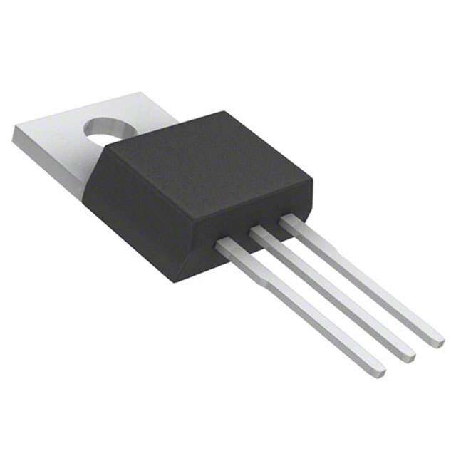
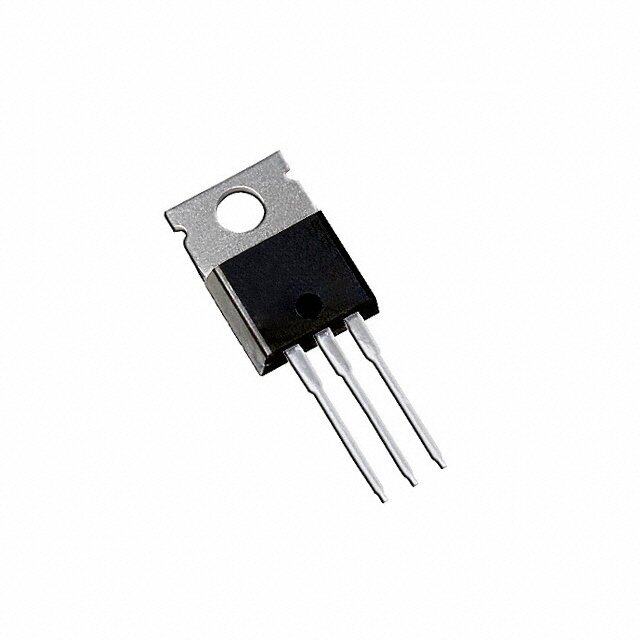
| 供应商器件封装 | TO-220-3 |
| 其它图纸 |
|
| 典型关闭延迟时间 | 40 ns |
| 功率-最大值 | 1.5W |
| 包装 | 散装 |
| 商标 | Diodes Incorporated |
| 安装类型 | 通孔 |
| 安装风格 | Through Hole |
| 封装 | Reel |
| 封装/外壳 | TO-220-3 |
| 封装/箱体 | TO-220-3 |
| 工厂包装数量 | 1000 |
| 晶体管极性 | P-Channel |
| 最大工作温度 | + 150 C |
| 最小工作温度 | - 55 C |
| 标准包装 | 50 |
| 漏源极电压(Vdss) | 35V |
| 电流-连续漏极(Id)(25°C时) | 3.3A (Ta), 12A (Tc) |
| 通道模式 | Enhancement |
| 配置 | Single |


PDF Datasheet 数据手册内容提取
ZXM64P035L3 35V P-CHANNEL ENHANCEMENT MODE MOSFET SUMMARY V(BR)DSS= -35V:RDS(on)= 0.075 : ID= -12A DESCRIPTION ThisnewgenerationofhighcelldensityplanarMOSFETsfromZetexutilisesaunique structurethatcombinesthebenefitsoflowon-resistancewithfastswitchingspeed.This makes them ideal for high efficiency, low voltage, power management applications. FEATURES (cid:1) Low on-resistance (cid:1) Fast switching speed (cid:1) Low threshold (cid:1) Low gate drive (cid:1) TO220 package APPLICATIONS (cid:1) 100W Class D Audio Output Stage (cid:1) Motor Control ORDERING INFORMATION DEVICE MULTIPLES ZXM64P035L3 1000 DEVICE MARKING (cid:1) ZXM6 Front View 4P035 ISSUE 1 - JUNE 2004 1
ZXM64P035L3 ABSOLUTE MAXIMUM RATING PARAMETER SYMBOL LIMIT UNIT Drain-SourceVoltage VDSS -35 V Gate-SourceVoltage VGS (cid:1)20 V ContinuousDrainCurrent(VGS=-10V;TC=25°C)(a) ID -12 A (VGS=-10V;TA=25°C)(b) -3.3 PulsedDrainCurrent(b) IDM -19 A ContinuousSourceCurrent(BodyDiode)(b) IS -2.3 A PulsedSourceCurrent(BodyDiode)(b) ISM -19 A PowerDissipationatTA=25°C(a) PD 20 W 160 mW/°C LinearDeratingFactor PowerDissipationatTA=25°C(b) PD 1.5 W 12 mW/°C LinearDeratingFactor OperatingandStorageTemperatureRange Tj:Tstg -55to+150 °C THERMAL RESISTANCE PARAMETER SYMBOL VALUE UNIT JunctiontoCase(a) RθJC 6.25 °C/W JunctiontoAmbient(b) RθJA 83.3 °C/W ISSUE 1 - JUNE 2004 2
ZXM64P035L3 ELECTRICAL CHARACTERISTICS(at T = 25°C unless otherwise stated). A PARAMETER SYMBOL MIN. TYP. MAX. UNIT CONDITIONS. STATIC Drain-Source BreakdownVoltage V(BR)DSS -35 V ID=-250µA,VGS=0V ZeroGateVoltageDrainCurrent IDSS -1 (cid:2)A VDS=-35V,VGS=0V Gate-BodyLeakage IGSS (cid:1)100 nA VGS=(cid:1)20V,VDS=0V Gate-SourceThresholdVoltage VGS(th) -1.0 V ID=-250(cid:2)A,VDS=VGS StaticDrain-SourceOn-StateResistance RDS(on) 0.075 (cid:3) VGS=-10V,ID=-2.4A (1) 0.105 (cid:3) VGS=-4.5V,ID=-1.2A ForwardTransconductance(1)(3) gfs 2.3 S VDS=-10V,ID=-1.2A DYNAMIC(3) InputCapacitance Ciss 825 pF VDS=-25V,VGS=0V, OutputCapacitance Coss 250 pF f=1MHz ReverseTransferCapacitance Crss 80 pF SWITCHING(2)(3) Turn-OnDelayTime td(on) 4.4 ns RiseTime tr 6.2 ns VDD=-15V,ID=-2.4A Turn-OffDelayTime td(off) 40 ns RG=6.0(cid:3),VGS=-10V FallTime tf 29.2 ns TotalGateCharge Qg 46 nC VDS=-24V,VGS=-10V, Gate-SourceCharge Qgs 9 nC I =-2.4A D Gate-DrainCharge Qgd 11.5 nC SOURCE-DRAINDIODE DiodeForwardVoltage(1) VSD -0.95 V TJ=25(cid:4)C,IS=-2.4A, VGS=0V ReverseRecoveryTime(3) trr 30.2 ns TJ=25(cid:4)C,IF=-2.4A, di/dt=100A/(cid:2)s ReverseRecoveryCharge(3) Qrr 27.8 nC NOTES (1) Measured under pulsed conditions. Width=300(cid:2)s. Duty cycle(cid:5)2% . (2) Switching characteristics are independent of operating junction temperature. (3) For design aid only, not subject to production testing. ISSUE 1 - JUNE 2004 3
ZXM64P035L3 Package Outline Package Dimensions DIM Millimetres Inches Min Max Min Max A 3.56 4.82 0.140 0.189 b 0.38 1.01 0.015 0.040 b1 1.15 1.77 0.045 0.070 c1 0.41 0.50 0.016 0.020 D 14.23 16.51 0.560 0.650 E 9.66 10.66 0.380 0.419 e 2.29 2.79 0.090 0.110 e1 4.83 5.33 0.190 0.210 F 0.51 1.39 0.20 0.055 H1 5.58 6.85 0.230 0.270 J1 2.04 2.92 0.080 0.115 L 12.70 14.73 0.500 0.580 L1 (cid:6) 6.35 (cid:6) 0.250 (cid:7)P 3.54 4.08 0.139 0.160 Q 2.54 3.42 0.100 0.134 ©Zetexplc 2001 Zetexplc ZetexGmbH ZetexInc Zetex(Asia) Ltd Fields New Road Streitfeldstraße19 700 Veterans Memorial Hwy 3701-04Metroplaza, Tower 1 Chadderton D-81673 München Hauppauge, NY11788 HingFongRoad Oldham, OL9 8NP KwaiFong United Kingdom Germany USA Hong Kong Telephone (44) 161 622 4422 Telefon: (49) 89 45 49 49 0 Telephone: (631) 360 2222 Telephone: (852) 26100 611 Fax: (44) 161 622 4420 Fax: (49) 89 45 49 49 49 Fax: (631) 360 8222 Fax: (852) 24250 494 These offices are supported by agents and distributors in major countries world-wide. Thispublicationisissuedtoprovideoutlineinformationonlywhich(unlessagreedbytheCompanyinwriting)maynotbeused,appliedorreproduced foranypurposeorformpartofanyorderorcontractorberegardedasarepresentationrelatingtotheproductsorservicesconcerned.TheCompany reserves the right to alter without notice the specification, design, price or conditions of supply of any product or service. Forthelatestproductinformation,logontowww.zetex.com ISSUE 1 - JUNE 2004 4