ICGOO在线商城 > 集成电路(IC) > 嵌入式 - 微控制器 > XS1-L16A-128-QF124-C10
 Datasheet下载
- 型号: XS1-L16A-128-QF124-C10
- 制造商: XMOS LIMITED
- 库位|库存: xxxx|xxxx
- 要求:
| 数量阶梯 | 香港交货 | 国内含税 |
| +xxxx | $xxxx | ¥xxxx |
查看当月历史价格
查看今年历史价格
XS1-L16A-128-QF124-C10产品简介:
ICGOO电子元器件商城为您提供XS1-L16A-128-QF124-C10由XMOS LIMITED设计生产,在icgoo商城现货销售,并且可以通过原厂、代理商等渠道进行代购。 XS1-L16A-128-QF124-C10价格参考。XMOS LIMITEDXS1-L16A-128-QF124-C10封装/规格:嵌入式 - 微控制器, XCore 微控制器 IC XS1 32 位 16 核 1000MIPS 128KB(32K x 32) SRAM 124-QFN 双列(10x10)。您可以下载XS1-L16A-128-QF124-C10参考资料、Datasheet数据手册功能说明书,资料中有XS1-L16A-128-QF124-C10 详细功能的应用电路图电压和使用方法及教程。
XMOS的XS1-L16A-128-QF124-C10是一款高性能嵌入式微控制器,适用于多种应用场景。以下是其主要应用领域:

 1. 音频处理与语音识别
该微控制器具有强大的并行处理能力,特别适合用于音频信号处理和语音识别系统。它能够实时处理多个音频通道,支持复杂的音频算法,如回声消除、噪声抑制和波束成形等。典型应用场景包括智能音箱、语音助手、车载娱乐系统等。

 2. 工业自动化
在工业自动化领域,XS1-L16A-128-QF124-C10可以用于控制复杂的工业设备和机器人。它支持多线程编程,能够同时处理多个任务,如传感器数据采集、电机控制和通信协议管理。此外,其低延迟特性使其非常适合实时控制系统,如PLC(可编程逻辑控制器)和运动控制系统。

 3. 物联网(IoT)设备
这款微控制器具备丰富的外设接口和强大的网络连接能力,非常适合用于物联网设备。它可以作为智能家居、智能城市或工业物联网系统的中央控制器,负责数据采集、处理和传输。通过集成Wi-Fi、蓝牙或以太网模块,它能够实现设备之间的无缝通信。

 4. 人机交互界面
XS1-L16A-128-QF124-C10可以用于开发高效的人机交互界面(HMI),如触摸屏控制器、手势识别系统和语音控制面板。它能够快速响应用户的输入,并提供流畅的用户体验。此外,其多核架构使得它可以在处理复杂图形和音频的同时保持系统的稳定性和响应速度。

 5. 汽车电子
在汽车电子领域,该微控制器可以用于车载信息娱乐系统、驾驶辅助系统和车身控制系统。它能够处理来自多个传感器的数据,执行复杂的控制算法,并与其他车载系统进行高效通信。例如,在高级驾驶辅助系统(ADAS)中,它可以帮助实现车道偏离预警、自动紧急制动等功能。

总之,XS1-L16A-128-QF124-C10凭借其卓越的性能和灵活性,广泛应用于音频处理、工业自动化、物联网、人机交互和汽车电子等多个领域。
| 参数 | 数值 |
| 产品目录 | 集成电路 (IC) |
| 描述 | IC MCU 32BIT 128KB SRAM 124QFN |
| EEPROM容量 | - |
| 产品分类 | |
| I/O数 | 84 |
| 品牌 | XMOS |
| 数据手册 | http://xmos.com/published/xs1-l16a-128-qf124-datasheet?version=latesthttp://www.xmos.com/published/xcore-multicore-microcontrollers-overview?version=latesthttp://www.xmos.com/published/xs1-lg-general-purpose-mmcus-product-brief?version=latesthttp://www.xmos.com/published/xs1-l-system-specification?version=latest |
| 产品图片 |
|
| 产品型号 | XS1-L16A-128-QF124-C10 |
| PCN零件编号 | |
| RAM容量 | - |
| rohs | 无铅 / 符合限制有害物质指令(RoHS)规范要求 |
| 产品系列 | XS1 |
| 供应商器件封装 | 124-QFN 双列(10x10) |
| 其它名称 | 880-1020 |
| 包装 | 托盘 |
| 外设 | - |
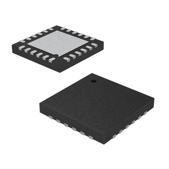
| 封装/外壳 | 124-TQFN 双排裸露焊盘 |
| 工作温度 | 0°C ~ 70°C |
| 振荡器类型 | 外部 |
| 数据转换器 | - |
| 标准包装 | 184 |
| 核心处理器 | XCore |
| 核心尺寸 | 32 位 16 核 |
| 电压-电源(Vcc/Vdd) | 0.95 V ~ 3.6 V |
| 程序存储器类型 | SRAM |
| 程序存储容量 | 128KB(32K x 32) |
| 连接性 | 可配置 |
| 速度 | 500MIPS |
| 配用 | /product-detail/zh/XK-SN-1BH12-E/880-1086-ND/4878859/product-detail/zh/XK-SN-1BQ12-E/880-1087-ND/4878858 |


PDF Datasheet 数据手册内容提取
XS1-L16A-128-QF124 Datasheet 2015/04/14 DocumentNumber:X8006, XMOS©2015,AllRightsReserved
XS1-L16A-128-QF124Datasheet 1 Table of Contents 1 xCOREMulticoreMicrocontrollers. . . . . . . . . . . . . . . . . . . . . . . . . . . . . . 2 2 XS1-L16A-128-QF124Features . . . . . . . . . . . . . . . . . . . . . . . . . . . . . . . 4 3 PinConfiguration . . . . . . . . . . . . . . . . . . . . . . . . . . . . . . . . . . . . . . . 5 4 SignalDescription . . . . . . . . . . . . . . . . . . . . . . . . . . . . . . . . . . . . . . . 6 5 ProductOverview . . . . . . . . . . . . . . . . . . . . . . . . . . . . . . . . . . . . . . . 10 6 PLL. . . . . . . . . . . . . . . . . . . . . . . . . . . . . . . . . . . . . . . . . . . . . . . . 13 7 BootProcedure. . . . . . . . . . . . . . . . . . . . . . . . . . . . . . . . . . . . . . . . . 14 8 Memory . . . . . . . . . . . . . . . . . . . . . . . . . . . . . . . . . . . . . . . . . . . . . 16 9 JTAG . . . . . . . . . . . . . . . . . . . . . . . . . . . . . . . . . . . . . . . . . . . . . . . 18 10 BoardIntegration . . . . . . . . . . . . . . . . . . . . . . . . . . . . . . . . . . . . . . . 19 11 DCandSwitchingCharacteristics . . . . . . . . . . . . . . . . . . . . . . . . . . . . . . 24 12 PackageInformation . . . . . . . . . . . . . . . . . . . . . . . . . . . . . . . . . . . . . 28 13 OrderingInformation . . . . . . . . . . . . . . . . . . . . . . . . . . . . . . . . . . . . . 29 Appendices . . . . . . . . . . . . . . . . . . . . . . . . . . . . . . . . . . . . . . . . . . . . . . 30 A ConfigurationoftheXS1 . . . . . . . . . . . . . . . . . . . . . . . . . . . . . . . . . . . 30 B ProcessorStatusConfiguration . . . . . . . . . . . . . . . . . . . . . . . . . . . . . . . 32 C TileConfiguration . . . . . . . . . . . . . . . . . . . . . . . . . . . . . . . . . . . . . . . 41 D NodeConfiguration . . . . . . . . . . . . . . . . . . . . . . . . . . . . . . . . . . . . . . 49 E XMOSUSBInterface . . . . . . . . . . . . . . . . . . . . . . . . . . . . . . . . . . . . . . 56 F DeviceErrata . . . . . . . . . . . . . . . . . . . . . . . . . . . . . . . . . . . . . . . . . . 56 G JTAG,xSCOPEandDebugging . . . . . . . . . . . . . . . . . . . . . . . . . . . . . . . . 57 H SchematicsDesignCheckList . . . . . . . . . . . . . . . . . . . . . . . . . . . . . . . . 59 I PCBLayoutDesignCheckList . . . . . . . . . . . . . . . . . . . . . . . . . . . . . . . . 62 J AssociatedDesignDocumentation . . . . . . . . . . . . . . . . . . . . . . . . . . . . . 63 K RelatedDocumentation . . . . . . . . . . . . . . . . . . . . . . . . . . . . . . . . . . . . 63 L RevisionHistory . . . . . . . . . . . . . . . . . . . . . . . . . . . . . . . . . . . . . . . . 64 TOOURVALUEDCUSTOMERS Itisourintentiontoprovideyouwithaccurateandcomprehensivedocumentationforthehardwareand softwarecomponentsusedinthisproduct. Tosubscribetoreceiveupdates,visithttp://www.xmos.com/. XMOSLtd.istheownerorlicenseeoftheinformationinthisdocumentandisprovidingittoyou“ASIS”with nowarrantyofanykind,expressorimpliedandshallhavenoliabilityinrelationtoitsuse. XMOSLtd.makes norepresentationthattheinformation,oranyparticularimplementationthereof,isorwillbefreefromany claimsofinfringementandagain,shallhavenoliabilityinrelationtoanysuchclaims. XMOSandtheXMOSlogoareregisteredtrademarksofXMOSLtdintheUnitedKingdomandothercountries, andmaynotbeusedwithoutwrittenpermission. Companyandproductnamesmentionedinthisdocument arethetrademarksorregisteredtrademarksoftheirrespectiveowners. X8006, XS1-L16A-128-QF124
XS1-L16A-128-QF124Datasheet 2 1 xCORE Multicore Microcontrollers The XS1-L Series is a comprehensive range of 32-bit multicore microcontrollers thatbringsthelowlatencyandtimingdeterminismofthexCOREarchitectureto mainstreamembeddedapplications. Unlikeconventionalmicrocontrollers,xCORE multicore microcontrollers execute multiple real-time tasks simultaneously and communicatebetweentasksusingahighspeednetwork. BecausexCOREmulticore microcontrollersarecompletelydeterministic,youcanwritesoftwaretoimplement functionsthattraditionallyrequirededicatedhardware. Security xTIME: schedulers SRAM JTAG PLL OTP ROM timers, clocks 64KB debug xCORE logical core xCORE logical core Hardware s I/O Pins repspoortnsse xxxxCCCCOOOORRRREEEE llllooooggggiiiiccccaaaallll ccccoooorrrreeee xCONNECThannels, link c xCORE logical core xCORE logical core xCORE logical core xCORE logical core Hardware I/O Pins repspoortnsse xxxCCCOOORRREEE lllooogggiiicccaaalll cccooorrreee CONNECTnnels, links xCORE logical core xha c Figure1: xCORE logical core XS1-LSeries: xCORE logical core 4-16core Security xTIME: schedulers SRAM JTAG PLL devices OTP ROM timers, clocks 64KB debug KeyfeaturesoftheXS1-L16A-128-QF124include: (cid:183) Tiles: DevicesconsistofoneormorexCOREtiles. Eachtilecontainsbetween fourandeight32-bitxCOREswithhighlyintegratedI/Oandon-chipmemory. (cid:183) LogicalcoresEachlogicalcorecanexecutetaskssuchascomputationalcode, DSP code, control software (including logic decisions and executing a state machine)orsoftwarethathandlesI/O.Section5.1 (cid:183) xTIMEschedulerThexTIMEschedulerperformsfunctionssimilartoanRTOS, in hardware. It services and synchronizes events in a core, so there is no requirementforinterrupthandlerroutines. ThexTIMEschedulertriggerscores oneventsgeneratedbyhardwareresourcessuchastheI/Opins,communication channelsandtimers. Oncetriggered,acorerunsindependentlyandconcurrently toothercores,untilitpausestowaitformoreevents. Section5.2 X8006, XS1-L16A-128-QF124
XS1-L16A-128-QF124Datasheet 3 (cid:183) ChannelsandchannelendsTasksrunningonlogicalcorescommunicateusing channelsformedbetweentwochannelends. Datacanbepassedsynchronously orasynchronouslybetweenthechannelendsassignedtothecommunicating tasks. Section5.5 (cid:183) xCONNECT Switch and LinksBetweentiles, channel communicationsareim- plemented over a high performance network of xCONNECT Links and routed throughahardwarexCONNECTSwitch. Section5.6 (cid:183) PortsTheI/OpinsareconnectedtotheprocessingcoresbyHardwareResponse ports. Theportlogiccandriveitspinshighandlow,oritcansamplethevalue onitspinsoptionallywaitingforaparticularcondition. Section5.3 (cid:183) ClockblocksxCOREdevicesincludeasetofprogrammableclockblocksthat canbeusedtogoverntherateatwhichportsexecute. Section5.4 (cid:183) MemoryEachxCORETileintegratesabankofSRAMforinstructionsanddata, andablockofone-timeprogrammable(OTP)memorythatcanbeconfiguredfor systemwidesecurityfeatures. Section8 (cid:183) PLLThePLLisusedtocreateahigh-speedprocessorclockgivenalowspeed externaloscillator. Section6 (cid:183) JTAGTheJTAGmodulecanbeusedforloadingprograms,boundaryscantesting, in-circuitsource-leveldebuggingandprogrammingtheOTPmemory. Section9 1.1 Software DevicesareprogrammedusingC,C++orxC(Cwithmulticoreextensions). XMOS provides tested and proven software libraries, which allow you to quickly add interfaceandprocessorfunctionalitysuchasUSB,Ethernet,PWM,graphicsdriver, andaudioEQtoyourapplications. 1.2 xTIMEcomposer Studio ThexTIMEcomposerStudiodevelopmentenvironmentprovidesallthetoolsyou needtowriteanddebugyourprograms,profileyourapplication,andwriteimages into flash memory or OTP memory on the device. Because xCORE devices oper- atedeterministically,theycanbesimulatedlikehardwarewithinxTIMEcomposer: uniquelyintheembeddedworld,xTIMEcomposerStudiothereforeincludesastatic timinganalyzer,cycle-accuratesimulator,andhigh-speedin-circuitinstrumenta- tion. xTIMEcomposercanbedrivenfromeitheragraphicaldevelopmentenvironment, orthecommandline. ThetoolsaresupportedonWindows,LinuxandMacOSX and available at no cost from xmos.com/downloads. Information on using the toolsisprovidedinthexTIMEcomposerUserGuide,X3766. X8006, XS1-L16A-128-QF124
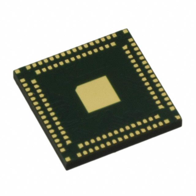
XS1-L16A-128-QF124Datasheet 4 2 XS1-L16A-128-QF124 Features (cid:183) MulticoreMicrocontrollerwithAdvancedMulti-CoreRISCArchitecture • 16real-timelogicalcoreson2xCOREtiles • Coresshareupto1000MIPS • Eachlogicalcorehas: — Guaranteedthroughputofbetween1/4and1/8oftileMIPS — 16x32bitdedicatedregisters • 159high-density16/32-bitinstructions — Allhavesingleclock-cycleexecution(exceptfordivide) — 32x32→64-bit MAC instructions for DSP, arithmetic and user-definable cryptographic functions (cid:183) ProgrammableI/O • 84general-purposeI/Opins,configurableasinputoroutput — Upto32x1bitport,12x4bitport,7x8bitport,3x16bitport — 4xCONNECTlinks • Portsamplingratesofupto60MHzwithrespecttoanexternalclock • 64channelendsforcommunicationwithothercores,onoroff-chip (cid:183) Memory • 128KBinternalsingle-cycleSRAM(max64KBpertile)forcodeanddatastorage • 16KBinternalOTP(max8KBpertile)forapplicationbootcode (cid:183) Hardwareresources • 12clockblocks(6pertile) • 20timers(10pertile) • 8locks(4pertile) (cid:183) JTAGModuleforOn-ChipDebug (cid:183) SecurityFeatures • Programminglockdisablesdebugandpreventsread-backofmemorycontents • AESbootloaderensuressecrecyofIPheldonexternalflashmemory (cid:183) AmbientTemperatureRange • Commercialqualification: 0°Cto70°C • Industrialqualification: -40°Cto85°C (cid:183) SpeedGrade • 10: 1000MIPS • 8: 800MIPS (cid:183) PowerConsumption • ActiveMode — 400mAat500MHz(typical) — 320mAat400MHz(typical) • StandbyMode — 28mA (cid:183) 124-pindual-rowQFNpackage0.5mmpitch X8006, XS1-L16A-128-QF124
XS1-L16A-128-QF124Datasheet 5 3 Pin Configuration A1 A68 A67 A66 A65 A64 A63 A62 A61 A60 A59 A58 A57 A56 A55 A54 A53 A52 GND VDD X0D25 X0D21 X0D20 X0D19 X0D18 X0D23 X0D17 X0D16 X0D15 X0D14 X0D13 X0D22 X0D12 X0D24 VDD GND B56 B55 B54 B53 B52 B51 B50 B49 B48 B47 B46 B45 B44 B43 VDD X0D43 X0D42 X0D41 X0D40 X0D39 X0D38 X0D37 X0D36 X0D33 X0D32 X0D31 X0D30 VDD A2 A51 VDDIO VDDIO A3 B1 B42 A50 X0D35 VDDIO VDDIO X1D11 X0AD434 WPCBA2UK_E XB0D4129 XA1D4910 X0AD502 GPCBA3UTE_ XB0D4028 XA1D4809 X0AD603 VPDCBD4UI_O XB0D3927 XA1D4708 X0AD704 PVCBD5UD_ XB0D3826 XA1D4607 X0AD805 PCCBL6UK_ DEBBN3U7G_ XA1D4506 A9 B7 B36 A44 X0D06 CLK GND MODE[3] X1D05 A10 B8 B35 A43 X0D07 RST_N MODE[2] X1D04 A11 B9 B34 A42 X0D08 TDO MODE[1] X1D03 A12 B10 B33 A41 X0D09 TCK MODE[0] X1D02 XA0D1310 TBM11S OVBTC3P2C_ XA1D4001 A14 B12 B31 A39 X0D11 TDI X1D39 X1D00 XA0D1500 TRBNS13T_ XB1D3038 APAVL3DL8_D XA0D1601 VDB1D4IO VDB2D9IO APAGL3NL7_D A17 A36 VDDIO VDDIO B15 B16 B17 B18 B19 B20 B21 B22 B23 B24 B25 B26 B27 B28 VDD X1D26 X1D27 X1D28 X1D29 X1D30 X1D31 X1D32 X1D33 X1D34 X1D35 X1D36 X1D37 VDD A18 A19 A20 A21 A22 A23 A24 A25 A26 A27 A28 A29 A30 A31 A32 A33 A34 A35 GND VDD X1D24 X1D12 X1D22 X1D13 X1D14 X1D15 X1D16 X1D17 X1D23 X1D18 X1D19 X1D20 X1D21 X1D25 VDD MODE[4] X8006, XS1-L16A-128-QF124
XS1-L16A-128-QF124Datasheet 6 4 Signal Description ThissectionliststhesignalsandI/OpinsavailableontheXS1-L16A-128-QF124. Thedeviceprovidesacombinationof1bit,4bit,8bitand16bitports,aswellas widerportsthatarefullyorpartially(gray)bondedout. Allpinsofaportprovide eitheroutputorinput,butsignalsindifferentdirectionscannotbemappedonto thesameport. Pinsmayhaveoneormoreofthefollowingproperties: (cid:183) PD/PU: The IO pin a weak pull-down or pull-up resistor. On GPIO pins this resistorcanbeenabled. (cid:183) ST:TheIOpinhasaSchmittTriggeronitsinput. Powerpins(6) Signal Function Type Properties GND Digitalground GND OTP_VCC OTPpowersupply PWR PLL_AGND AnaloggroundforPLL GND PLL_AVDD AnalogPLLpower PWR VDD Digitaltilepower PWR VDDIO DigitalI/Opower PWR Clockspins(2) Signal Function Type Properties CLK PLLreferenceclock Input PD,ST MODE[4:0] Bootmodeselect Input PU,ST JTAGpins(7) Signal Function Type Properties DEBUG_N Multi-chipdebug I/O PU RST_N Globalresetinput Input PU,ST TCK Testclock Input PU,ST TDI Testdatainput Input PU,ST TDO Testdataoutput Output PD,OT TMS Testmodeselect Input PU,ST TRST_N Testresetinput Input PU,ST I/Opins(84) Signal Function Type Properties X0D00 1A0 I/O PDS,RS (continued) X8006, XS1-L16A-128-QF124
XS1-L16A-128-QF124Datasheet 7 Signal Function Type Properties X0D01 XLA4out 1B0 I/O PDS,RS X0D02 XLA3out 4A0 8A0 16A0 32A20 I/O PDS,RU X0D03 XLA2out 4A1 8A1 16A1 32A21 I/O PDS,RU X0D04 XLA1out 4B0 8A2 16A2 32A22 I/O PDS,RU X0D05 XLA0out 4B1 8A3 16A3 32A23 I/O PDS,RU X0D06 XLA0in 4B2 8A4 16A4 32A24 I/O PDS,RU X0D07 XLA1in 4B3 8A5 16A5 32A25 I/O PDS,RU X0D08 XLA2in 4A2 8A6 16A6 32A26 I/O PDS,RU X0D09 XLA3in 4A3 8A7 16A7 32A27 I/O PDS,RU X0D10 XLA4in 1C0 I/O PDS,RS X0D11 1D0 I/O PDS,RS X0D12 1E0 I/O PDS,RU X0D13 XLB4out 1F0 I/O PDS,RU X0D14 XLB3out 4C0 8B0 16A8 32A28 I/O PDS,RU X0D15 XLB2out 4C1 8B1 16A9 32A29 I/O PDS,RU X0D16 XLB1out 4D0 8B2 16A10 I/O PDS,RU X0D17 XLB0out 4D1 8B3 16A11 I/O PDS,RU X0D18 XLB0in 4D2 8B4 16A12 I/O PDS,RU X0D19 XLB1in 4D3 8B5 16A13 I/O PDS,RU X0D20 XLB2in 4C2 8B6 16A14 32A30 I/O PDS,RU X0D21 XLB3in 4C3 8B7 16A15 32A31 I/O PDS,RU X0D22 XLB4in 1G0 I/O PDS,RU X0D23 1H0 I/O PDS,RU X0D24 1I0 I/O PDS X0D25 1J0 I/O PDS X0D26 4E0 8C0 16B0 I/O PDS,RU X0D27 4E1 8C1 16B1 I/O PDS,RU X0D28 4F0 8C2 16B2 I/O PDS,RU X0D29 4F1 8C3 16B3 I/O PDS,RU X0D30 4F2 8C4 16B4 I/O PDS,RU X0D31 4F3 8C5 16B5 I/O PDS,RU X0D32 4E2 8C6 16B6 I/O PDS,RU X0D33 4E3 8C7 16B7 I/O PDS,RU X0D34 1K0 I/O PDS X0D35 1L0 I/O PDS X0D36 1M0 8D0 16B8 I/O PDS X0D37 1N0 8D1 16B9 I/O PDS,RU X0D38 1O0 8D2 16B10 I/O PDS,RU X0D39 1P0 8D3 16B11 I/O PDS,RU X0D40 8D4 16B12 I/O PDS,RU X0D41 8D5 16B13 I/O PDS,RU X0D42 8D6 16B14 I/O PDS,RU X0D43 8D7 16B15 I/O PUS,RU (continued) X8006, XS1-L16A-128-QF124
XS1-L16A-128-QF124Datasheet 8 Signal Function Type Properties X1D00 1A0 I/O PDS,RS X1D01 XLA4out 1B0 I/O PDS,RS X1D02 XLA3out 4A0 8A0 16A0 32A20 I/O PDS,RU X1D03 XLA2out 4A1 8A1 16A1 32A21 I/O PDS,RU X1D04 XLA1out 4B0 8A2 16A2 32A22 I/O PDS,RU X1D05 XLA0out 4B1 8A3 16A3 32A23 I/O PDS,RU X1D06 XLA0in 4B2 8A4 16A4 32A24 I/O PDS,RU X1D07 XLA1in 4B3 8A5 16A5 32A25 I/O PDS,RU X1D08 XLA2in 4A2 8A6 16A6 32A26 I/O PDS,RU X1D09 XLA3in 4A3 8A7 16A7 32A27 I/O PDS,RU X1D10 XLA4in 1C0 I/O PDS,RS X1D11 1D0 I/O PDS,RS X1D12 1E0 I/O PDS,RU X1D13 XLB4out 1F0 I/O PDS,RU X1D14 XLB3out 4C0 8B0 16A8 32A28 I/O PDS,RU X1D15 XLB2out 4C1 8B1 16A9 32A29 I/O PDS,RU X1D16 XLB1out 4D0 8B2 16A10 I/O PDS,RU X1D17 XLB0out 4D1 8B3 16A11 I/O PDS,RU X1D18 XLB0in 4D2 8B4 16A12 I/O PDS,RU X1D19 XLB1in 4D3 8B5 16A13 I/O PDS,RU X1D20 XLB2in 4C2 8B6 16A14 32A30 I/O PDS,RU X1D21 XLB3in 4C3 8B7 16A15 32A31 I/O PDS,RU X1D22 XLB4in 1G0 I/O PDS,RU X1D23 1H0 I/O PDS,RU X1D24 1I0 I/O PDS X1D25 1J0 I/O PDS X1D26 4E0 8C0 16B0 I/O PDS,RU X1D27 4E1 8C1 16B1 I/O PDS,RU X1D28 4F0 8C2 16B2 I/O PDS,RU X1D29 4F1 8C3 16B3 I/O PDS,RU X1D30 4F2 8C4 16B4 I/O PDS,RU X1D31 4F3 8C5 16B5 I/O PDS,RU X1D32 4E2 8C6 16B6 I/O PDS,RU X1D33 4E3 8C7 16B7 I/O PDS,RU X1D34 1K0 I/O PDS X1D35 1L0 I/O PDS X1D36 1M0 8D0 16B8 I/O PDS X1D37 1N0 8D1 16B9 I/O PDS,RU X1D38 1O0 8D2 16B10 I/O PDS,RU X1D39 1P0 8D3 16B11 I/O PDS,RU X8006, XS1-L16A-128-QF124
XS1-L16A-128-QF124Datasheet 9 pins(5) Signal Function Type Properties PCU_CLK Clockinput PCU_GATE Powercontrolgatecontrol PCU_VDD PCUtilepower PCU_VDDIO PCUI/Osupply PCU_WAKE Wakeupreset X8006, XS1-L16A-128-QF124
XS1-L16A-128-QF124Datasheet 10 5 Product Overview TheXS1-L16A-128-QF124isapowerfuldevicethatconsistsoftwoxCORETiles, eachcomprisingaflexiblelogicalprocessingcoreswithtightlyintegratedI/Oand on-chipmemory. 5.1 Logical cores Eachtilehas8activelogicalcores,whichissueinstructionsdownasharedfour- stage pipeline. Instructions from the active cores are issued round-robin. If up tofourlogicalcoresareactive,eachcoreisallocatedaquarteroftheprocessing cycles. Ifmorethanfourlogicalcoresareactive,eachcoreisallocatedatleast1/n cycles(forncores).Figure2showstheguaranteedcoreperformancedepending onthenumberofcoresused. Speed MIPS Frequency MinimumMIPSpercore(forncores) Figure2: grade 1 2 3 4 5 6 7 8 Logicalcore 8 800MIPS 400MHz 100 100 100 100 80 67 57 50 performance 10 1000MIPS 500MHz 125 125 125 125 100 83 71 63 Thereisnowaythattheperformanceofalogicalcorecanbereducedbelowthese predicted levels. Because cores may be delayed on I/O, however, their unused processing cycles can be taken by other cores. This means that for more than fourlogicalcores,theperformanceofeachcoreisoftenhigherthanthepredicted minimumbutcannotbeguaranteed. Thelogicalcoresaretriggeredbyeventsinsteadofinterruptsandruntocompletion. Alogicalcorecanbepausedtowaitforanevent. 5.2 xTIME scheduler ThexTIMEschedulerhandlestheeventsgeneratedbyxCORETileresources,such aschannelends,timersandI/Opins. Itensuresthatalleventsareservicedand synchronized,withouttheneedforanRTOS.EventsthatoccurattheI/Opinsare handledbytheHardware-ResponseportsandfeddirectlytotheappropriatexCORE Tile. AnxCORETilecanalsochoosetowaitforaspecifiedtimetoelapse,orfor datatobecomeavailableonachannel. Tasks do not need to be prioritised as each of them runs on their own logical xCORE. It is possible to share a set of low priority tasks on a single core using cooperativemultitasking. 5.3 Hardware Response Ports Hardware Response ports connect an xCORE tile to one or more physical pins andassuchdefinetheinterfacebetweenhardwareattachedtotheXS1-L16A-128- QF124,andthesoftwarerunningonit. Acombinationof1bit,4bit,8bit,16bitand 32bitportsareavailable. Allpinsofaportprovideeitheroutputorinput. Signals indifferentdirectionscannotbemappedontothesameport. X8006, XS1-L16A-128-QF124
XS1-L16A-128-QF124Datasheet 11 clock port reference clock clock block readyOut readyIn port port counter conditional port value logic stamp/time PORT FIFO port transfer PINS SERDES CORE value register Figure3: Portblock output (drive) input (sample) diagram Theportlogiccandriveitspinshighorlow,oritcansamplethevalueonitspins, optionallywaitingforaparticularcondition. Portsareaccessedusingdedicated instructionsthatareexecutedinasingleprocessorcycle. DataistransferredbetweenthepinsandcoreusingaFIFOthatcomprisesaSERDES andtransferregister,providingoptionsforserializationandbuffereddata. Eachporthasa16-bitcounterthatcanbeusedtocontrolthetimeatwhichdatais transferredbetweentheportvalueandtransferregister. Thecountervaluescan beobtainedatanytimetofindoutwhendatawasobtained,orusedtodelayI/O untilsometimeinthefuture. Theportcountervalueisautomaticallysavedasa timestamp,thatcanbeusedtoprovideprecisecontrolofresponsetimes. The ports and xCONNECT links are multiplexed onto the physical pins. If an xConnectLinkisenabled,thepinsoftheunderlyingportsaredisabled. Ifaport isenabled,itoverrulesportswithhigherwidthsthatsharethesamepins. Thepins onthewiderportthatarenotsharedremainavailableforusewhenthenarrower portisenabled. Portsalwaysoperateattheirspecifiedwidth,eveniftheyshare pinswithanotherport. 5.4 Clock blocks xCOREdevicesincludeasetofprogrammableclockscalledclockblocksthatcan beusedtogoverntherateatwhichportsexecute. EachxCOREtilehassixclock blocks: thefirstclockblockprovidesthetilereferenceclockandrunsatadefault frequencyof100MHz; theremainingclockblockscanbesettorunatdifferent frequencies. Aclockblockcanusea1-bitportasitsclocksourceallowingexternalapplication clockstobeusedtodrivetheinputandoutputinterfaces. X8006, XS1-L16A-128-QF124
XS1-L16A-128-QF124Datasheet 12 100MHz reference divider 1-bit port clock ... ... readyIn Figure4: clock block Clockblock diagram port counter InmanycasesI/Osignalsareaccompaniedbystrobingsignals. ThexCOREports caninputandinterpretstrobe(knownasreadyInandreadyOut)signalsgenerated byexternalsources,andportscangeneratestrobesignalstoaccompanyoutput data. Onreset,eachportisconnectedtoclockblock0,whichrunsfromthexCORETile referenceclock. 5.5 Channels and Channel Ends Logicalcorescommunicateusingpoint-to-pointconnections,formedbetweentwo channelends. Achannel-endisaresourceonanxCOREtile,thatisallocatedby theprogram. Eachchannel-endhasauniquesystem-wideidentifierthatcomprises auniquenumberandtheirtileidentifier. Dataistransmittedtoachannel-endby anoutput-instruction;andtheothersideexecutesaninput-instruction. Datacan bepassedsynchronouslyorasynchronouslybetweenthechannelends. 5.6 xCONNECT Switch and Links XMOSdevicesprovideascalablearchitecture,wheremultiplexCOREdevicescan beconnectedtogethertoformonesystem. EachxCOREdevicehasanxCONNECT interconnectthatprovidesacommunicationinfrastructureforalltasksthatrunon thevariousxCOREtilesonthesystem. TheinterconnectreliesonacollectionofswitchesandXMOSlinks. EachxCORE devicehasanon-chipswitchthatcansetupcircuitsorroutedata. Theswitches areconnectedbyxConnectLinks. AnXMOSlinkprovidesaphysicalconnection between two switches. The switch has a routing algorithm that supports many differenttopologies,includinglines,meshes,trees,andhypercubes. The links operate in either 2 wires per direction or 5 wires per direction mode, depending on the amount of bandwidth required. Circuit switched, streaming andpacketswitcheddatacanbothbesupportedefficiently. Streamsprovidethe fastestpossibledataratesbetweenxCORETiles(upto250MBit/s),buteachstream requires a single link to be reserved between switches on two tiles. All packet communicationscanbemultiplexedontoasinglelink. X8006, XS1-L16A-128-QF124
XS1-L16A-128-QF124Datasheet 13 xCONNECT Link to another device switch CORE CORE CORE CORE CORE CORE CORE CORE xCONNECT CORE CORE switch CORE CORE Figure5: CORE Switch,links CORE CORE CORE andchannel ends xCORE Tile xCORE Tile Information on the supported routing topologies that can be used to connect multipledevicestogethercanbefoundintheXS1-LLinkPerformanceandDesign Guide,X2999. 6 PLL ThePLLcreatesahigh-speedclockthatisusedfortheswitch,tile,andreference clock. ThePLLmultiplicationvalueisselectedthroughthetwoMODEpins,andcanbe changedbysoftwaretospeedupthetileoruselesspower. TheMODEpinsareset asshowninFigure6: Oscillator MODE Tile PLLRatio PLLsettings Frequency 1 0 Frequency OD F R 5-13MHz 0 0 130-399.75MHz 30.75 1 122 0 Figure6: PLLmultiplier 13-20MHz 1 1 260-400.00MHz 20 2 119 0 valuesand 20-48MHz 1 0 167-400.00MHz 8.33 2 49 0 MODEpins 48-100MHz 0 1 196-400.00MHz 4 2 23 0 Figure6alsoliststhevaluesofOD,F andR,whicharetheregistersthatdefine theratioofthetilefrequencytotheoscillatorfrequency: F+1 1 1 F =F × × × core osc 2 R+1 OD+1 X8006, XS1-L16A-128-QF124
XS1-L16A-128-QF124Datasheet 14 OD,F andR mustbechosensothat0≤R≤63,0≤F ≤4095,0≤OD≤7,and 260MHz≤F × F+1 × 1 ≤1.3GHz. TheOD,F,andR valuescanbemodified osc 2 R+1 bywritingtothedigitalnodePLLconfigurationregister. TheMODEpinsmustbeheldatastaticvalueduringandafterdeassertionofthe systemreset. If a different tile frequency is required (eg, 500 MHz), then the PLL must be reprogrammedafterboottoprovidetherequiredtilefrequency. TheXMOStools performthisoperationbydefault. Furtherdetailsonconfiguringtheclockcanbe foundintheXS1-LClockFrequencyControldocument,X1433. 7 Boot Procedure ThedeviceiskeptinresetbydrivingRST_Nlow. Wheninreset,allGPIOpinsare highimpedance. WhenthedeviceistakenoutofresetbyreleasingRST_N the processorstartsitsinternalresetprocess. After15-150µs(dependingontheinput clock), allGPIOpinshavetheirinternalpull-resistorenabled, andtheprocessor bootsataclockspeedthatdependsonMODE0andMODE1. The xCORE Tile boot procedure is illustrated in Figure 7. In normal usage, MODE[4:2] controls the boot source according to the table in Figure 8. If bit 5ofthesecurityregister(see§8.1)isset,thedevicebootsfromOTP. Start Boot ROM Primary boot No Security Register Bit [5] set Yes Copy OTP contents Boot according to OTP to base of SRAM boot source pins Figure7: Boot procedure Execute program Thebootimagehasthefollowingformat: (cid:183) A32-bitprogramsizes inwords. (cid:183) Programconsistingofs×4bytes. (cid:183) A32-bitCRC,orthevalue0x0D15AB1EtoindicatethatnoCRCcheckshouldbe performed. X8006, XS1-L16A-128-QF124
XS1-L16A-128-QF124Datasheet 15 MODE MODE MODE BootSource [4] [3] [2] X 0 0 None: DevicewaitstobebootedviaJTAG X 0 1 Reserved 0 1 0 Tile0bootsfromlinkB,Tile1fromchannelend0viaTile0 0 1 1 Tile0bootsfromSPI,Tile1fromchannelend0viaTile0 Figure8: 1 1 0 Tile0andTile1independentlyenablelinkBandinternallinks Bootsource (E,F,G,H),andbootfromchannelend0 pins 1 1 1 Tile0andTile1bootfromSPIindependently The program size and CRC are stored least significant byte first. The program is loaded into the lowest memory address of RAM, and the program is started fromthataddress. TheCRCiscalculatedoverthebytestreamrepresentedbythe programsizeandtheprogramitself. Thepolynomialusedis0xEDB88320(IEEE 802.3);theCRCregisterisinitializedwith0xFFFFFFFFandtheresidueisinverted toproducetheCRC. 7.1 Boot from SPI master If set to boot from SPI master, the processor enables the four pins specified in Figure9,anddrivestheSPIclockat2.5MHz(assuminga400MHzcoreclock). A READcommandisissuedwitha24-bitaddress0x000000. Theclockpolarityand phaseare0/0. Pin Signal Description X0D00 MISO MasterInSlaveOut(Data) Figure9: X0D01 SS SlaveSelect SPImaster X0D10 SCLK Clock pins X0D11 MOSI MasterOutSlaveIn(Data) ThexCORETileexpectseachbytetobetransferredwiththeleast-significantbit first. ProgrammerswhowritebytesintoanSPIinterfaceusingthemostsignificant bitfirstmayhavetoreversethebitsineachbyteoftheimagestoredintheSPI device. Ifalargebootimageistobereadin,itisfastertofirstloadasmallboot-loader thatreadsthelargeimageusingafasterSPIclock,forexample50MHzorasfast astheflashdevicesupports. ThepinsusedforSPIbootarehardcodedinthebootROMandcannotbechanged. Ifrequired,anSPIbootprogramcanbeburnedintoOTPthatusesdifferentpins. 7.2 Boot from xConnect Link If set to boot from an xConnect Link, the processor enables Link B around 200 nsafterthebootprocessstarts. EnablingtheLinkswitchesoffthepull-downon X8006, XS1-L16A-128-QF124
XS1-L16A-128-QF124Datasheet 16 resistors X0D16..X0D19, drives X0D16 and X0D17 low (the initial state for the Link), and monitors pins X0D18 and X0D19 for boot-traffic. X0D18 and X0D19 mustbelowatthisstage. Iftheinternalpull-downistooweaktodrainanyresidual charge,externalpull-downsof10Kmayberequiredonthosepins. Theboot-romonthecorewillthen: 1. Allocatechannel-end0. 2. Inputawordonchannel-end0. Itwillusethiswordasachanneltoacknowledge theboot. Providethenull-channel-end0x0000FF02ifnoacknowledgmentis required. 3. Inputthebootimagespecifiedabove,includingtheCRC. 4. InputanENDcontroltoken. 5. OutputanENDcontroltokentothechannel-endreceivedinstep2. 6. Freechannel-end0. 7. Jumptotheloadedcode. 7.3 Boot from OTP If an xCORE tile is set to use secure boot (see Figure 7), the boot image is read fromaddress0oftheOTPmemoryinthetile’ssecuritymodule. This feature can be used to implement a secure bootloader which loads an en- cryptedimagefromexternalflash,decryptsandCRCchecksitwiththeprocessor, and discontinues the boot process if the decryption or CRC check fails. XMOS provides a default secure bootloader that can be written to the OTP along with secretdecryptionkeys. EachtilehasitsownindividualOTPmemory,andhencesometilescanbebooted fromOTPwhileothersarebootedfromSPIorthechannelinterface. Thisenables systems to be partially programmed, dedicating one or more tiles to perform a particularfunction,leavingtheothertilesuser-programmable. 7.4 Security register The security register enables security features on the xCORE tile. The features shown in Figure 10 provide a strong level of protection and are sufficient for providingstrongIPsecurity. 8 Memory 8.1 OTP EachxCORETileintegrates8KBone-timeprogrammable(OTP)memoryalongwith asecurityregisterthatconfiguressystemwidesecurityfeatures. TheOTPholds X8006, XS1-L16A-128-QF124
XS1-L16A-128-QF124Datasheet 17 Feature Bit Description DisableJTAG 0 TheJTAGinterfaceisdisabled,makingitimpossible forthetilestateormemorycontenttobeaccessed viatheJTAGinterface. DisableLinkaccess 1 Othertilesareforbiddenaccesstotheprocessorstate viathesystemswitch. DisablingbothJTAGandLink accesstransformsanxCORETileintoa“secureisland” withothertilesfreefornon-secureuserapplication code. SecureBoot 5 ThexCORETileisforcedtobootfromaddress0of the OTP, allowing the xCORE Tile boot ROM to be bypassed(see§7). Redundantrows 7 EnablesredundantrowsinOTP. SectorLock0 8 DisableprogrammingofOTPsector0. SectorLock1 9 DisableprogrammingofOTPsector1. SectorLock2 10 DisableprogrammingofOTPsector2. SectorLock3 11 DisableprogrammingofOTPsector3. OTPMasterLock 12 DisableOTPprogrammingcompletely: disablesup- datestoallsectorsandsecurityregister. DisableJTAG-OTP 13 Disableall(read&write)accessfromtheJTAGinter- facetothisOTP. DisableGlobalDebug 14 DisablesaccesstotheDEBUG_Npin. Figure10: 21..15 Generalpurposesoftwareaccessablesecurityregister Security availabletoend-users. register 31..22 General purpose user programmable JTAG UserID features codeextension. data in four sectors each containing 512 rows of 32 bits which can be used to implement secure bootloaders and store encryption keys. Data for the security registerisloadedfromtheOTPonpowerup. AlladditionaldatainOTPiscopied fromtheOTPtoSRAMandexecutedfirstontheprocessor. TheOTPmemoryisprogrammedusingthreespecialI/Oports: theOTPaddress portisa16-bitportwithresourceID0x100200,theOTPdataiswrittenviaa32-bit portwithresourceID0x200100,andtheOTPcontrolisona16-bitportwithID 0x100300. Programmingisperformedthroughlibotpandxburn. 8.2 SRAM Each xCORE Tile integrates a single 64KBSRAM bank for both instructions and data. All internal memory is 32 bits wide, and instructions are either 16-bit or 32-bit. Byte(8-bit),half-word(16-bit)orword(32-bit)accessesaresupportedand areexecutedwithinonetileclockcycle. Thereisnodedicatedexternalmemory interface,althoughdatamemorycanbeexpandedthroughappropriateuseofthe ports. X8006, XS1-L16A-128-QF124
XS1-L16A-128-QF124Datasheet 18 9 JTAG The JTAG module can be used for loading programs, boundary scan testing, in- circuitsource-leveldebuggingandprogrammingtheOTPmemory. X0 X1 BS TAP CHIP TAP BS TAP CHIP TAP TDI TDI TDO TDI TDO TDI TDO TDI TDO TDO TCK TMS Figure11: TRST_N JTAGchain structure DEBUG_N TheJTAGchainstructureisillustratedinFigure11. Directlyafterreset,twoTAP controllersarepresentintheJTAGchainforeachxCORETile: theboundaryscan TAPandthechipTAP.TheboundaryscanTAPisastandard1149.1compliantTAP thatcanbeusedforboundaryscanoftheI/Opins. ThechipTAPprovidesaccess intothexCORETile,switchandOTPforloadingcodeanddebugging. TheTRST_Npinmustbeassertedlowduringandafterpowerupfor100ns. IfJTAG isnotrequired,theTRST_NpincanbetiedtogroundtoholdtheJTAGmodulein reset. TheDEBUG_NpinisusedtosynchronizethedebuggingofmultiplexCORETiles. Thispincanoperateinbothoutputandinputmode. Inoutputmodeandwhen configuredtodoso,DEBUG_Nisdrivenlowbythedevicewhentheprocessorhits adebugbreakpoint. Priortothispointthepinwillbetri-stated. Ininputmode and when configured to do so, driving this pin low will put the xCORE Tile into debugmode. SoftwarecansetthebehaviorofthexCORETilebasedonthispin. This pin should have an external pull up of 4K7-47KΩ or left not connected in singlecoreapplications. TheJTAGdeviceidentificationregistercanbereadbyusingtheIDCODEinstruction. ItscontentsarespecifiedinFigure12. Bit31 DeviceIdentificationRegister Bit0 Figure12: Version PartNumber ManufacturerIdentity 1 IDCODE 0 0 0 0 0 0 0 0 0 0 0 0 0 0 0 0 0 0 1 0 0 1 1 0 0 0 1 1 0 0 1 1 returnvalue 0 0 0 0 2 6 3 3 X8006, XS1-L16A-128-QF124
XS1-L16A-128-QF124Datasheet 19 TheJTAGusercoderegistercanbereadbyusingtheUSERCODEinstruction. Its contentsarespecifiedinFigure13. TheOTPUserIDfieldisreadfrombits[22:31] of the security register on xCORE Tile 0, see §8.1 (all zero on unprogrammed devices). Bit31 UsercodeRegister Bit0 Figure13: OTPUserID Unused SiliconRevision USERCODE 0 0 0 0 0 0 0 0 0 0 0 0 0 0 1 0 1 0 0 0 0 0 0 0 0 0 0 0 0 0 0 0 returnvalue 0 0 0 2 8 0 0 0 9.1 PCU PCU_WAKEshouldbeleftunconnected,PCU_GATEshouldbeleftunconnectedand PCU_CLKmustbetiedtoCLK. 10 Board Integration Thedevicehasthefollowingpowersupplypins: (cid:183) VDDpinsforthexCORETile (cid:183) VDDIOpinsfortheI/Olines (cid:183) PLL_AVDDpinsforthePLL (cid:183) PCU_VDDandPCU_VDDIOpinsforthePCU (cid:183) OTP_VCCpinsfortheOTP Severalpinsofeachtypeareprovidedtominimizetheeffectofinductancewithin thepackage,allofwhichmustbeconnected. Thepowersuppliesmustbebrought upmonotonicallyandinputvoltagesmustnotexceedspecificationatanytime. The VDD supply must ramp from 0V to its final value within 10ms to ensure correctstartup. TheVDDIOandOTP_VCCsupplymustramptoitsfinalvaluebeforeVDDreaches 0.4V. The PLL_AVDD supply should be separated from the other noisier supplies on theboard. ThePLLrequiresaverycleanpowersupply,andalowpassfilter(for example,a2.2Ωresistorand100nFmulti-layerceramiccapacitor)isrecommended onthispin. ThePCU_VDDsupplymustbeconnectedtotheVDDsupply. ThePCU_VDDIOsupplymustbeconnectedtotheVDDIOsupply. TheOTP_VCCsupplyshouldbeconnectedtotheVDDIOsupply. Thefollowinggroundpinsareprovided: X8006, XS1-L16A-128-QF124
XS1-L16A-128-QF124Datasheet 20 (cid:183) PLL_AGNDforPLL_AVDD (cid:183) GNDforallothersupplies Allgroundpinsmustbeconnecteddirectlytotheboardground. The VDD and VDDIO supplies should be decoupled close to the chip by several 100nF low inductance multi-layer ceramic capacitors between the supplies and GND (for example, 4x100nF 0402 low inductance MLCCs per supply rail). The groundsideofthedecouplingcapacitorsshouldhaveasshortapathbacktothe GND pins as possible. A bulk decoupling capacitor of at least 10uF should be placedoneachofthesesupplies. RST_N is an active-low asynchronous-assertion global reset signal. Following a reset,thePLLre-establisheslockafterwhichthedevicebootsupaccordingtothe bootmode(see§7).RST_Nandmustbeassertedlowduringandafterpowerup for100ns. 10.1 Land patterns and solder stencils ThelandpatternrecommendationsinthisdocumentarebasedonaRoHScompliant processandderived,wherepossible,fromthenominalGenericRequirementsfor SurfaceMountDesignandLandPatternStandardsIPC-7351Bspecifications. This standard aims to achieve desired targets of heel, toe and side fillets for solder- joints. Solderpasteandgroundviarecommendationsarebasedonourengineeringand developmentkitboardproduction. Theyhavebeenfoundtoworkandoptimized asappropriatetoachieveahighyield. Thesize,typeandnumberofviasusedin thecenterpadaffectshowmuchsolderwicksdowntheviasduringreflow. Thisin turn,alongwithsolderpastercoverage,affectsthefinalassembledpackageheight. Thesefactorsshouldbetakenintoaccountduringdesignandmanufacturingof thePCB. Thefollowinglandpatternsandsolderpastecontainsrecommendations. Finalland patternandsolderpastedecisionsaretheresponsibilityofthecustomer. These shouldbetunedduringmanufacturetosuitthemanufacturingprocess. Thepackageisa124pindualrowQuadFlatNoleadpackagewithexposedheat slugona0.5mmpitch. AnexamplelandpatternisshowninFigure14. Padwidthsandspacingsaresuchthatsoldermaskcanstillbeappliedbetweenthe padsusingstandarddesignrules. Thisishighlyrecommendedtoreducesolder shortsbetweenpads. SeetherecommendedPCBsoldermaskdiagraminFigure 15. 10.2 Solder Stencil ThesolderjointsintheQFNpackageareformedexclusivelyfromthesolderpaste depositedfromthesolderstencil. Atthesmallaperturesizesrequired,thedesign ofthestencilbecomesimportanttoensureareliablefinalsolderjointvolumeand reliablesolderjoints. X8006, XS1-L16A-128-QF124
XS1-L16A-128-QF124Datasheet 21 9.50 0.75 1.00 4.00 2.80 2.80 7.50 Figure14: Exampleland 1.00 pattern 0.30x0.30 0.50 0.5mm 0.4mm PAD PAD PAD SOLDERMASK 0.75mm 0.3mm PAD PAD PAD Figure15: Detailof 0.1mm outerpads 0.3mm X8006, XS1-L16A-128-QF124
XS1-L16A-128-QF124Datasheet 22 ThesolderstencilrecommendationsherearebasedonthosesuggestedintheIPC specificationIPC-7525A"StencilDesignGuidelines". Astheaperturesizeinthestencilbecomesverysmall,theamountofsolderwhich remains on the PCB pad after printing is reduced. This occurs due to friction betweenthewallsofthestencilandthesolderpastedraggingthepastefromthe padwhenthestencilisremoved. Thiseffectisminimizedasthethicknessofthe stencilisreduced. Forthe124pinQFNpackage,ourrecommendationsaretousea4milthicklaser cutstencil. Thesolderstencilaperturesforthepadsshouldbe0.3mmsquarewith 0.06mmradiusedcorners. Thisisthesamesizeasthepadsthemselvesapartfrom radiusedcornerstoaidinpastetransfer. ThiscanbeseenintheFigure16. Soldermask 0.3mm Copper Pad Solderpaste Figure16: Solderstencil forouter pads 0.3mm Thesedimensionsshouldbethefinalaperturesizesusedonthestencil,thisshould beagreedwiththestencilmakersorassemblyhouse. Itiscommonforassembly houses to subject the paste mask data to a global undersize before cutting the stencil. Ifthisundersizeisappliedtothesesmallaperturesthepastetransferis likelytobepoorandopensolderjointsmayresult. Forthecenterpadofthispackage,foursquaresofsolderpasteisrecommended, 1mmonasideasshowninFigure17. Thisgivesapastetopadarearatioof51%. 10.3 Ground and Thermal Vias ViasundertheheatslugintothegroundplaneofthePCBarerecommendedfora lowinductancegroundconnectionandgoodthermalperformance. A3x3gridof vias,witha0.6mmdiameterannularringanda0.3mmdrill,equallyspacedacross theheatslug,wouldbesuitable. 10.4 Moisture Sensitivity XMOSdevicesare,likeallsemiconductordevices,susceptibletomoistureabsorp- tion. Whenremovedfromthesealedpackaging,thedevicesslowlyabsorbmoisture fromthesurroundingenvironment. Ifthelevelofmoisturepresentinthedevice istoohighduringreflow,damagecanoccurduetotheincreasedinternalvapour pressureofmoisture. Exampledamagecanincludebondwiredamage,dielifting, internalorexternalpackagecracksand/ordelamination. X8006, XS1-L16A-128-QF124
XS1-L16A-128-QF124Datasheet 23 2.8mm 1.0mm 2.8mm 0.3mm Soldermask Figure17: Copper Pad Solderstencil Solderpaste forcentre pad 0.3mm 1.0mm AllXMOSdevicesareMoistureSensitivityLevel(MSL)3-deviceshaveashelflife of 168 hours between removal from the packaging and reflow, provided they are stored below 30C and 60% RH. If devices have exceeded these values or an includedmoistureindicatorcardshowsexcessivelevelsofmoisture,thentheparts shouldbebakedasappropriatebeforeuse. ThisisbasedoninformationfromJoint IPC/JEDECStandardForMoisture/ReflowSensitivityClassificationForNonhermetic SolidStateSurface-MountDevicesJ-STD-020RevisionD. X8006, XS1-L16A-128-QF124
XS1-L16A-128-QF124Datasheet 24 11 DC and Switching Characteristics 11.1 Operating Conditions Symbol Parameter MIN TYP MAX UNITS Notes VDD TileDCsupplyvoltage 0.95 1.00 1.05 V VDDIO I/Osupplyvoltage 3.00 3.30 3.60 V PLL_AVDD PLLanalogsupply 0.95 1.00 1.05 V PCU_VDD PCUtileDCsupplyvoltage 0.95 1.00 1.05 V PCU_VDDIO PCUI/ODCsupplyvoltage 3.00 3.30 3.60 V OTP_VCC OTPsupplyvoltage 3.00 3.30 3.60 V Cl xCORETileI/Oload 25 pF capacitance Ambientoperating 0 70 °C Ta temperature(Commercial) Ambientoperating -40 85 °C Figure18: temperature(Industrial) Operating Tj Junctiontemperature 125 °C conditions Tstg Storagetemperature -65 150 °C 11.2 DC Characteristics Symbol Parameter MIN TYP MAX UNITS Notes V(IH) Inputhighvoltage 2.00 3.60 V A V(IL) Inputlowvoltage -0.30 0.70 V A V(OH) Outputhighvoltage 2.00 V B,C Figure19: V(OL) Outputlowvoltage 0.60 V B,C DCcharacter- R(PU) Pull-upresistance 35K Ω D istics R(PD) Pull-downresistance 35K Ω D A Allpinsexceptpowersupplypins. B Ports1A,1D,1E,1H,1I,1J,1Kand1Larenominal8mAdrivers,theremainderofthe general-purposeI/Osare4mA. C Measuredwith4mAdriverssourcing4mA,8mAdriverssourcing8mA. D UsedtoguaranteelogicstateforanI/Owhenhighimpedance.Theinternalpull-ups/pull-downs shouldnotbeusedtopullexternalcircuitry. 11.3 ESD Stress Voltage Figure20: Symbol Parameter MIN TYP MAX UNITS Notes ESDstress HBM Humanbodymodel -2.00 2.00 KV voltage MM Machinemodel -200 200 V X8006, XS1-L16A-128-QF124
XS1-L16A-128-QF124Datasheet 25 11.4 Reset Timing Symbol Parameters MIN TYP MAX UNITS Notes Figure21: T(RST) Resetpulsewidth 5 us Resettiming T(INIT) Initializationtime 150 µs A A ShowsthetimetakentostartbootingafterRST_Nhasgonehigh. 11.5 Power Consumption Symbol Parameter MIN TYP MAX UNITS Notes I(DDCQ) QuiescentVDDcurrent 28 mA A,B,C PD Tilepowerdissipation 450 µW/MIPS A,D,E,F ActiveVDDcurrent(SpeedGrade 320 600 mA A,G IDD 8) Figure22: ActiveVDDcurrent(SpeedGrade 400 750 mA A,H xCORETile 10) currents I(ADDPLL) PLL_AVDDcurrent 14 mA I A Useforbudgetarypurposesonly. B AssumestypicaltileandI/Ovoltageswithnoswitchingactivity. C IncludesPLLcurrent. D AssumestypicaltileandI/Ovoltageswithnominalswitchingactivity. E Assumes1MHz=1MIPS. F PD(TYP)valueistheusagepowerconsumptionundertypicaloperatingconditions. G Measurementconditions:VDD=1.0V,VDDIO=3.3V,25°C,400MHz,averagedeviceresource usage. H Measurementconditions:VDD=1.0V,VDDIO=3.3V,25°C,500MHz,averagedeviceresource usage. I PLL_AVDD=1.0V The tile power consumption of the device is highly application dependent and shouldbeusedforbudgetarypurposesonly. More detailed power analysis can be found in the XS1-L Power Consumption document,X2999. X8006, XS1-L16A-128-QF124
XS1-L16A-128-QF124Datasheet 26 11.6 Clock Symbol Parameter MIN TYP MAX UNITS Notes f Frequency 4.22 20 100 MHz SR Slewrate 0.10 V/ns TJ(LT) Longtermjitter(pk-pk) 2 % A Processorclockfrequency(Speed 400 MHz B f(MAX) Grade8) Figure23: Processorclockfrequency(Speed 500 MHz B Clock Grade10) A PercentageofCLKperiod. B AssumestypicaltileandI/Ovoltageswithnominalactivity. Further details can be found in the XS1-L Clock Frequency Control document, X1433. 11.7 xCORE Tile I/O AC Characteristics Symbol Parameter MIN TYP MAX UNITS Notes T(XOVALID) Inputdatavalidwindow 8 ns Figure24: T(XOINVALID) Outputdatainvalidwindow 9 ns I/OACchar- T(XIFMAX) Rateatwhichdatacanbesampled 60 MHz acteristics withrespecttoanexternalclock Theinputvalidwindowparameterrelatestothecapabilityofthedevicetocapture datainputtothechipwithrespecttoanexternalclocksource. Itiscalculatedasthe sumoftheinputsetuptimeandinputholdtimewithrespecttotheexternalclock asmeasuredatthepins. Theoutputinvalidwindowspecifiesthetimeforwhich anoutputisinvalidwithrespecttotheexternalclock. Notethattheseparameters arespecifiedasawindowratherthanabsolutenumberssincethedeviceprovides functionalitytodelaytheincomingclockwithrespecttotheincomingdata. Informationoninterfacingtohigh-speedsynchronousinterfacescanbefoundin theXS1PortI/OTimingdocument,X5821. 11.8 xConnect Link Performance Symbol Parameter MIN TYP MAX UNITS Notes B(2blinkP) 2blinkbandwidth(packetized) 87 MBit/s A,B Figure25: B(5blinkP) 5blinkbandwidth(packetized) 217 MBit/s A,B Link B(2blinkS) 2blinkbandwidth(streaming) 100 MBit/s B performance B(5blinkS) 5blinkbandwidth(streaming) 250 MBit/s B A Assumes32-bytepacketin3-byteheadermode.Actualperformancedependsonsizeoftheheader andpayload. B 7.5nssymboltime. X8006, XS1-L16A-128-QF124
XS1-L16A-128-QF124Datasheet 27 TheasynchronousnatureoflinksmeansthattherelativephasingofCLKclocksis notimportantinamulti-clocksystem,providingeachmeetstherequiredstability criteria. 11.9 JTAG Timing Symbol Parameter MIN TYP MAX UNITS Notes f(TCK_D) TCKfrequency(debug) 18 MHz f(TCK_B) TCKfrequency(boundaryscan) 10 MHz T(SETUP) TDOtoTCKsetuptime 5 ns A Figure26: T(HOLD) TDOtoTCKholdtime 5 ns A JTAGtiming T(DELAY) TCKtooutputdelay 15 ns B A TimingappliestoTMSandTDIinputs. B TimingappliestoTDOoutputfromnegativeedgeofTCK. AllJTAGoperationsaresynchronoustoTCKapartfromtheglobalasynchronous resetTRST_N. X8006, XS1-L16A-128-QF124
XS1-L16A-128-QF124Datasheet 28 12 Package Information X8006, XS1-L16A-128-QF124
XS1-L16A-128-QF124Datasheet 29 12.1 Part Marking CC - Number of logical cores F - Product family R - RAM (in log-2) T - Temperature grade M - MIPS grade CCFRTM MC - Manufacturer MCYYWWXX YYWW - Date Figure27: XX - Reserved LLLLLL.LL Partmarking scheme Wafer lot code 13 Ordering Information ProductCode Marking Qualification SpeedGrade XS1–L16A–128–QF124–C8 16L7C8 Commercial 800MIPS Figure28: XS1–L16A–128–QF124–C10 16L7C10 Commercial 1000MIPS Orderable XS1–L16A–128–QF124–I8 16L7I8 Industrial 800MIPS partnumbers XS1–L16A–128–QF124–I10 16L7I10 Industrial 1000MIPS X8006, XS1-L16A-128-QF124
XS1-L16A-128-QF124Datasheet 30 Appendices A Configuration of the XS1 Thedeviceisconfiguredthroughthreebanksofregisters,asshowninFigure29. PLL Security xTIME: schedulers SRAM ProceJsTsAorG status OTP ROM timers, clocks 64KB rdegeibstuegrs xCORE logical core 0 xCORE logical core 1 Hardware ks I/O pins repspoortnsse xxxCCCOOORRREEE lllooogggiiicccaaalll cccooorrreee 234 rexgCtChannelsiiOsletReErs reNgoiONNECT linsdteers xCORE logical core 5 C x xCORE logical core 6 xCORE logical core 7 xCORE logical core 0 xCORE logical core 1 Hardware ks I/O pins repspoortnsse xxxCCCOOORRREEE lllooogggiiicccaaalll cccooorrreee 234 rexgCtChannelsiiOsletReErs reNgoiONNECT linsdteers xCORE logical core 5 C x xCORE logical core 6 xCORE logical core 7 Figure29: PLL Security xTIME: schedulers SRAM ProceJsTsAorG status Registers OTP ROM timers, clocks 64KB rdegeibstuegrs The following communication sequences specify how to access those registers. Anymessagestransmittedcontainthemostsignificant24bitsofthechannel-end to which a response is to be sent. This comprises the node-identifier and the channelnumberwithinthenode. ifnoresponseisrequiredonawriteoperation, supply24-bitswiththelast8-bitsset,whichsuppressesthereplymessage. Any multi-bytedataissentmostsignificantbytefirst. A.1 Accessing a processor status register Theprocessorstatusregistersareaccesseddirectlyfromtheprocessorinstruction set. TheinstructionsGETPSandSETPSreadandwriteaword. Theregisternumber should be translated into a processor-status resource identifier by shifting the registernumberleft8places,andORingitwith0x0C.Alternatively,thefunctions getps(reg)andsetps(reg,value)canbeusedfromXC. A.2 Accessing an xCORE Tile configuration register xCORETileconfigurationregisterscanbeaccessedthroughtheinterconnectusing the functions write_tile_config_reg(tileref, ...) and read_tile_config_reg(tile X8006, XS1-L16A-128-QF124
XS1-L16A-128-QF124Datasheet 31 (cid:62) ref, ...), where tileref is the name of the xCORE Tile, e.g. tile[1]. These functionsimplementtheprotocolsdescribedbelow. Insteadofusingthefunctionsabove,achannel-endcanbeallocatedtocommuni- catewiththexCOREtileconfigurationregisters. Thedestinationofthechannel-end shouldbesetto0xnnnnC20Cwherennnnnnisthetile-identifier. Awritemessagecomprisesthefollowing: control-token 24-bitresponse 16-bit 32-bit control-token 192 channel-endidentifier registernumber data 1 The response to a write message comprises either control tokens 3 and 1 (for success),orcontroltokens4and1(forfailure). Areadmessagecomprisesthefollowing: control-token 24-bitresponse 16-bit control-token 193 channel-endidentifier registernumber 1 Theresponsetothereadmessagecompriseseithercontroltoken3,32-bitofdata, andcontrol-token1(forsuccess),orcontroltokens4and1(forfailure). A.3 Accessing node configuration Node configuration registers can be accessed through the interconnect using thefunctionswrite_node_config_reg(device, ...)andread_node_config_reg(device, (cid:62) ...), where device is the name of the node. These functions implement the protocolsdescribedbelow. Insteadofusingthefunctionsabove,achannel-endcanbeallocatedtocommu- nicatewiththenodeconfigurationregisters. Thedestinationofthechannel-end shouldbesetto0xnnnnC30Cwherennnnisthenode-identifier. Awritemessagecomprisesthefollowing: control-token 24-bitresponse 16-bit 32-bit control-token 192 channel-endidentifier registernumber data 1 The response to a write message comprises either control tokens 3 and 1 (for success),orcontroltokens4and1(forfailure). Areadmessagecomprisesthefollowing: control-token 24-bitresponse 16-bit control-token 193 channel-endidentifier registernumber 1 Theresponsetoareadmessagecompriseseithercontroltoken3,32-bitofdata, andcontrol-token1(forsuccess),orcontroltokens4and1(forfailure). X8006, XS1-L16A-128-QF124
XS1-L16A-128-QF124Datasheet 32 B Processor Status Configuration Theprocessorstatuscontrolregisterscanbeaccesseddirectlybytheprocessor usingprocessorstatusreadsandwrites(usegetps(reg)andsetps(reg,value)for readsandwrites). Number Perm Description 0x00 RW RAMbaseaddress 0x01 RW Vectorbaseaddress 0x02 RW xCORETilecontrol 0x03 RO xCORETilebootstatus 0x05 RO Securityconfiguration 0x06 RW RingOscillatorControl 0x07 RO RingOscillatorValue 0x08 RO RingOscillatorValue 0x09 RO RingOscillatorValue 0x0A RO RingOscillatorValue 0x10 DRW DebugSSR 0x11 DRW DebugSPC 0x12 DRW DebugSSP 0x13 DRW DGETREGoperand1 0x14 DRW DGETREGoperand2 0x15 DRW Debuginterrupttype 0x16 DRW Debuginterruptdata 0x18 DRW Debugcorecontrol 0x20.. 0x27 DRW Debugscratch 0x30.. 0x33 DRW Instructionbreakpointaddress 0x40.. 0x43 DRW Instructionbreakpointcontrol 0x50.. 0x53 DRW Datawatchpointaddress1 0x60.. 0x63 DRW Datawatchpointaddress2 0x70.. 0x73 DRW Databreakpointcontrolregister 0x80.. 0x83 DRW Resourcesbreakpointmask Figure30: 0x90.. 0x93 DRW Resourcesbreakpointvalue Summary 0x9C.. 0x9F DRW Resourcesbreakpointcontrolregister X8006, XS1-L16A-128-QF124
XS1-L16A-128-QF124Datasheet 33 B.1 RAM base address: 0x00 ThisregistercontainsthebaseaddressoftheRAM.Itisinitializedto0x00010000. Bits Perm Init Description 0x00: RAMbase 31:2 RW Mostsignificant16bitsofalladdresses. address 1:0 RO - Reserved B.2 Vector base address: 0x01 Baseaddressofeventvectorsineachresource. Onaninterruptorevent,the16 mostsignificantbitsofthedestinationaddressareprovidedbythisregister;the leastsignificant16bitscomefromtheeventvector. Bits Perm Init Description 0x01: Vectorbase 31:16 RW Themostsignificantbitsforalleventandinterruptvectors. address 15:0 RO - Reserved B.3 xCORE Tile control: 0x02 RegistertocontrolfeaturesinthexCOREtile Bits Perm Init Description 31:6 RO - Reserved 5 RW 0 Setto1toselectthedynamicmodefortheclockdividerwhen theclockdividerisenabled.Indynamicmodetheclockdivideris onlyactivatedwhenallactivelogicalcoresarepaused. Instatic modetheclockdividerisalwaysenabled. 0x02: 4 RW 0 Setto1toenabletheclockdivider. ThisslowsdownthexCORE xCORETile tileclockinordertouselesspower. control 3:0 RO - Reserved B.4 xCORE Tile boot status: 0x03 Thisread-onlyregisterdescribesthebootstatusofthexCOREtile. X8006, XS1-L16A-128-QF124
XS1-L16A-128-QF124Datasheet 34 Bits Perm Init Description 31:24 RO - Reserved 23:16 RO xCOREtilenumberontheswitch. 15:9 RO - Reserved 0x03: 8 RO Setto1ifbootfromOTPisenabled. xCORETile 7:0 RO ThebootmodepinsMODE0,MODE1,...,specifyingtheboot bootstatus frequency,bootsource,etc. B.5 Security configuration: 0x05 CopyofthesecurityregisterasreadfromOTP. 0x05: Security Bits Perm Init Description configuration 31:0 RO Value. B.6 Ring Oscillator Control: 0x06 There are four free-running oscillators that clock four counters. The oscillators canbestartedandstoppedusingthisregister. Thecountersshouldonlyberead when the ring oscillator is stopped. The counter values can be read using four subsequentregisters. TheringoscillatorsareasynchronoustothexCOREtileclock andcanbeusedasasourceofrandombits. Bits Perm Init Description 0x06: 31:2 RO - Reserved Ring Oscillator 1 RW 0 Setto1toenablethexCOREtileringoscillators Control 0 RW 0 Setto1toenabletheperipheralringoscillators B.7 Ring Oscillator Value: 0x07 ThisregistercontainsthecurrentcountofthexCORETileCellringoscillator. This valueisnotresetonasystemreset. 0x07: Bits Perm Init Description Ring Oscillator 31:16 RO - Reserved Value 15:0 RO - Ringoscillatorcounterdata. X8006, XS1-L16A-128-QF124
XS1-L16A-128-QF124Datasheet 35 B.8 Ring Oscillator Value: 0x08 ThisregistercontainsthecurrentcountofthexCORETileWireringoscillator. This valueisnotresetonasystemreset. 0x08: Bits Perm Init Description Ring Oscillator 31:16 RO - Reserved Value 15:0 RO - Ringoscillatorcounterdata. B.9 Ring Oscillator Value: 0x09 ThisregistercontainsthecurrentcountofthePeripheralCellringoscillator. This valueisnotresetonasystemreset. 0x09: Bits Perm Init Description Ring Oscillator 31:16 RO - Reserved Value 15:0 RO - Ringoscillatorcounterdata. B.10 Ring Oscillator Value: 0x0A ThisregistercontainsthecurrentcountofthePeripheralWireringoscillator. This valueisnotresetonasystemreset. 0x0A: Bits Perm Init Description Ring Oscillator 31:16 RO - Reserved Value 15:0 RO - Ringoscillatorcounterdata. B.11 Debug SSR: 0x10 ThisregistercontainsthevalueoftheSSRregisterwhenthedebuggerwascalled. 0x10: Bits Perm Init Description DebugSSR 31:0 RO - Reserved B.12 Debug SPC: 0x11 ThisregistercontainsthevalueoftheSPCregisterwhenthedebuggerwascalled. X8006, XS1-L16A-128-QF124
XS1-L16A-128-QF124Datasheet 36 0x11: Bits Perm Init Description DebugSPC 31:0 DRW Value. B.13 Debug SSP: 0x12 ThisregistercontainsthevalueoftheSSPregisterwhenthedebuggerwascalled. 0x12: Bits Perm Init Description DebugSSP 31:0 DRW Value. B.14 DGETREG operand 1: 0x13 TheresourceIDofthelogicalcorewhosestateistoberead. Bits Perm Init Description 0x13: DGETREG 31:8 RO - Reserved operand1 7:0 DRW Threadnumbertoberead B.15 DGETREG operand 2: 0x14 RegisternumbertobereadbyDGETREG Bits Perm Init Description 0x14: DGETREG 31:5 RO - Reserved operand2 4:0 DRW Registernumbertoberead B.16 Debug interrupt type: 0x15 Registerthatspecifieswhatactivatedthedebuginterrupt. X8006, XS1-L16A-128-QF124
XS1-L16A-128-QF124Datasheet 37 Bits Perm Init Description 31:18 RO - Reserved 17:16 DRW If the debug interrupt was caused by a hardware breakpoint orhardwarewatchpoint,thisfieldcontainsthenumberofthe breakpoint or watchpoint. If multiple breakpoints or watch- pointstriggeratonce,thelowestnumberistaken. 15:8 DRW Ifthedebuginterruptwascausedbyalogicalcore,thisfield containsthenumberofthatcore. Otherwisethisfieldis0. 7:3 RO - Reserved 2:0 DRW 0 Indicatesthecauseofthedebuginterrupt 1: HostinitiatedadebuginterruptthroughJTAG 2: ProgramexecutedaDCALLinstruction 0x15: 3: Instructionbreakpoint Debug 4: Datawatchpoint interrupttype 5: Resourcewatchpoint B.17 Debug interrupt data: 0x16 Onadatawatchpoint,thisregistercontainstheeffectiveaddressofthememory operationthattriggeredthedebugger. Onaresourcewatchpoint,itcountainsthe resourceidentifier. 0x16: Debug Bits Perm Init Description interruptdata 31:0 DRW Value. B.18 Debug core control: 0x18 This register enables the debugger to temporarily disable logical cores. When returningfromthedebuginterrupts,thecoressetinthisregisterwillnotexecute. Thisenablessinglesteppingtobeimplemented. Bits Perm Init Description 31:8 RO - Reserved 0x18: 7:0 DRW 1-hotvectordefiningwhichlogicalcoresarestoppedwhennot Debugcore indebugmode. Everybitwhichissetpreventstherespective control logicalcorefromrunning. X8006, XS1-L16A-128-QF124
XS1-L16A-128-QF124Datasheet 38 B.19 Debug scratch: 0x20 .. 0x27 A set of registers used by the debug ROM to communicate with an external debugger,forexampleoverJTAG.ThisisthesamesetofregistersastheDebug ScratchregistersinthexCOREtileconfiguration. 0x20.. 0x27: Debug Bits Perm Init Description scratch 31:0 DRW Value. B.20 Instruction breakpoint address: 0x30 .. 0x33 Thisregistercontainstheaddressoftheinstructionbreakpoint. IfthePCmatches this address, then a debug interrupt will be taken. There are four instruction breakpointsthatarecontrolledindividually. 0x30.. 0x33: Instruction breakpoint Bits Perm Init Description address 31:0 DRW Value. B.21 Instruction breakpoint control: 0x40 .. 0x43 Thisregistercontrolswhichlogicalcoresmaytakeaninstructionbreakpoint,and underwhichcondition. Bits Perm Init Description 31:24 RO - Reserved 23:16 DRW 0 Abitforeachlogicalcoreinthetileallowingthebreakpointto beenabledindividuallyforeachlogicalcore. 15:2 RO - Reserved 0x40.. 0x43: 1 DRW 0 Set to 1 to cause an instruction breakpoint if the PC is not Instruction equaltothebreakpointaddress. Bydefault,thebreakpointis breakpoint triggeredwhenthePCisequaltothebreakpointaddress. control 0 DRW 0 When1theinstructionbreakpointisenabled. B.22 Data watchpoint address 1: 0x50 .. 0x53 Thissetofregisterscontainsthefirstaddressforthefourdatawatchpoints. X8006, XS1-L16A-128-QF124
XS1-L16A-128-QF124Datasheet 39 0x50.. 0x53: Data watchpoint Bits Perm Init Description address1 31:0 DRW Value. B.23 Data watchpoint address 2: 0x60 .. 0x63 Thissetofregisterscontainsthesecondaddressforthefourdatawatchpoints. 0x60.. 0x63: Data watchpoint Bits Perm Init Description address2 31:0 DRW Value. B.24 Data breakpoint control register: 0x70 .. 0x73 Thissetofregisterscontrolseachofthefourdatawatchpoints. Bits Perm Init Description 31:24 RO - Reserved 23:16 DRW 0 Abitforeachlogicalcoreinthetileallowingthebreakpointto beenabledindividuallyforeachlogicalcore. 15:3 RO - Reserved 2 DRW 0 Setto1toenablebreakpointstobetriggeredonloads. Break- pointsalwaystriggeronstores. 1 DRW 0 By default, data watchpoints trigger if memory in the range 0x70.. 0x73: [Address1..Address2]isaccessed(therangeisinclusiveofAd- Data dress1andAddress2). Ifsetto1,datawatchpointstriggerif breakpoint memory outside the range (Address2..Address1) is accessed control (therangeisexclusiveofAddress2andAddress1). register 0 DRW 0 When1theinstructionbreakpointisenabled. B.25 Resources breakpoint mask: 0x80 .. 0x83 Thissetofregisterscontainsthemaskforthefourresourcewatchpoints. X8006, XS1-L16A-128-QF124
XS1-L16A-128-QF124Datasheet 40 0x80.. 0x83: Resources breakpoint Bits Perm Init Description mask 31:0 DRW Value. B.26 Resources breakpoint value: 0x90 .. 0x93 Thissetofregisterscontainsthevalueforthefourresourcewatchpoints. 0x90.. 0x93: Resources breakpoint Bits Perm Init Description value 31:0 DRW Value. B.27 Resources breakpoint control register: 0x9C .. 0x9F Thissetofregisterscontrolseachofthefourresourcewatchpoints. Bits Perm Init Description 31:24 RO - Reserved 23:16 DRW 0 Abitforeachlogicalcoreinthetileallowingthebreakpointto beenabledindividuallyforeachlogicalcore. 15:2 RO - Reserved 0x9C.. 0x9F: 1 DRW 0 Bydefault,resourcewatchpointstriggerwhentheresourceid Resources maskedwiththesetMaskequalstheValue.Ifsetto1,resource breakpoint watchpointstriggerwhentheresourceidmaskedwiththeset control MaskisnotequaltotheValue. register 0 DRW 0 When1theinstructionbreakpointisenabled. X8006, XS1-L16A-128-QF124
XS1-L16A-128-QF124Datasheet 41 C Tile Configuration ThexCORETilecontrolregisterscanbeaccessedusingconfigurationreadsand writes (use write_tile_config_reg(tileref, ...) and read_tile_config_reg(tileref, (cid:62) ...)forreadsandwrites). Number Perm Description 0x00 RO Deviceidentification 0x01 RO xCORETiledescription1 0x02 RO xCORETiledescription2 0x04 CRW ControlPSwitchpermissionstodebugregisters 0x05 CRW Causedebuginterrupts 0x06 RW xCORETileclockdivider 0x07 RO Securityconfiguration 0x10.. 0x13 RO PLinkstatus 0x20.. 0x27 CRW Debugscratch 0x40 RO PCoflogicalcore0 0x41 RO PCoflogicalcore1 0x42 RO PCoflogicalcore2 0x43 RO PCoflogicalcore3 0x44 RO PCoflogicalcore4 0x45 RO PCoflogicalcore5 0x46 RO PCoflogicalcore6 0x47 RO PCoflogicalcore7 0x60 RO SRoflogicalcore0 0x61 RO SRoflogicalcore1 0x62 RO SRoflogicalcore2 0x63 RO SRoflogicalcore3 0x64 RO SRoflogicalcore4 0x65 RO SRoflogicalcore5 0x66 RO SRoflogicalcore6 Figure31: 0x67 RO SRoflogicalcore7 Summary 0x80.. 0x9F RO Chanendstatus X8006, XS1-L16A-128-QF124
XS1-L16A-128-QF124Datasheet 42 C.1 Device identification: 0x00 Bits Perm Init Description 31:24 RO ProcessorIDofthisxCOREtile. 23:16 RO NumberofthenodeinwhichthisxCOREtileislocated. 0x00: Device 15:8 RO xCOREtilerevision. identification 7:0 RO xCOREtileversion. C.2 xCORE Tile description 1: 0x01 This register describes the number of logical cores, synchronisers, locks and channelendsavailableonthisxCOREtile. Bits Perm Init Description 31:24 RO Numberofchannelends. 23:16 RO Numberoflocks. 0x01: xCORETile 15:8 RO Numberofsynchronisers. description1 7:0 RO - Reserved C.3 xCORE Tile description 2: 0x02 This register describes the number of timers and clock blocks available on this xCOREtile. Bits Perm Init Description 31:16 RO - Reserved 0x02: xCORETile 15:8 RO Numberofclockblocks. description2 7:0 RO Numberoftimers. C.4 Control PSwitch permissions to debug registers: 0x04 This register can be used to control whether the debug registers (marked with permissionCRW)areaccessiblethroughthetileconfigurationregisters. Whenthis bitisset,write-accesstothoseregistersisdisabled,preventingdebuggingofthe xCOREtileovertheinterconnect. X8006, XS1-L16A-128-QF124
XS1-L16A-128-QF124Datasheet 43 0x04: Control Bits Perm Init Description PSwitch permissions 31:1 RO - Reserved todebug 0 CRW Setto1torestrictPSwitchaccesstoallCRWmarkedregistersto registers becomeread-onlyratherthanread-write. C.5 Cause debug interrupts: 0x05 ThisregistercanbeusedtoraiseadebuginterruptinthisxCOREtile. Bits Perm Init Description 31:2 RO - Reserved 0x05: Causedebug 1 RO 0 Setto1whentheprocessorisindebugmode. interrupts 0 CRW 0 Setto1torequestadebuginterruptontheprocessor. C.6 xCORE Tile clock divider: 0x06 ThisregistercontainsthevalueusedtodividethePLLclocktocreatethexCORE tileclock. Thedividerisenabledundercontrolofthetilecontrolregister Bits Perm Init Description 0x06: xCORETile 31:8 RO - Reserved clockdivider 7:0 RW Valueoftheclockdividerminusone. C.7 Security configuration: 0x07 CopyofthesecurityregisterasreadfromOTP. 0x07: Security Bits Perm Init Description configuration 31:0 RO Value. C.8 PLink status: 0x10 .. 0x13 Statusofeachofthefourprocessorlinks;connectingthexCOREtiletotheswitch. X8006, XS1-L16A-128-QF124
XS1-L16A-128-QF124Datasheet 44 Bits Perm Init Description 31:26 RO - Reserved 25:24 RO 00-ChannelEnd,01-ERROR,10-PSCTL,11-Idle. 23:16 RO BasedonSRC_TARGET_TYPEvalue,itrepresentschannelEndID orIdlestatus. 15:6 RO - Reserved 5:4 RO Two-bitnetworkidentifier 3 RO - Reserved 2 RO 1whenthecurrentpacketisconsideredjunkandwillbethrown away. 1 RO 0 Setto1iftheswitchisroutingdataintothelink,andifaroute existsfromanotherlink. 0x10.. 0x13: 0 RO 0 Setto1ifthelinkisroutingdataintotheswitch,andifaroute PLinkstatus iscreatedtoanotherlinkontheswitch. C.9 Debug scratch: 0x20 .. 0x27 A set of registers used by the debug ROM to communicate with an external debugger, for example over the switch. This is the same set of registers as the DebugScratchregistersintheprocessorstatus. 0x20.. 0x27: Debug Bits Perm Init Description scratch 31:0 CRW Value. C.10 PC of logical core 0: 0x40 ValueofthePCoflogicalcore0. 0x40: PCoflogical Bits Perm Init Description core0 31:0 RO Value. X8006, XS1-L16A-128-QF124
XS1-L16A-128-QF124Datasheet 45 C.11 PC of logical core 1: 0x41 0x41: PCoflogical Bits Perm Init Description core1 31:0 RO Value. C.12 PC of logical core 2: 0x42 0x42: PCoflogical Bits Perm Init Description core2 31:0 RO Value. C.13 PC of logical core 3: 0x43 0x43: PCoflogical Bits Perm Init Description core3 31:0 RO Value. C.14 PC of logical core 4: 0x44 0x44: PCoflogical Bits Perm Init Description core4 31:0 RO Value. C.15 PC of logical core 5: 0x45 0x45: PCoflogical Bits Perm Init Description core5 31:0 RO Value. X8006, XS1-L16A-128-QF124
XS1-L16A-128-QF124Datasheet 46 C.16 PC of logical core 6: 0x46 0x46: PCoflogical Bits Perm Init Description core6 31:0 RO Value. C.17 PC of logical core 7: 0x47 0x47: PCoflogical Bits Perm Init Description core7 31:0 RO Value. C.18 SR of logical core 0: 0x60 ValueoftheSRoflogicalcore0 0x60: SRoflogical Bits Perm Init Description core0 31:0 RO Value. C.19 SR of logical core 1: 0x61 0x61: SRoflogical Bits Perm Init Description core1 31:0 RO Value. C.20 SR of logical core 2: 0x62 0x62: SRoflogical Bits Perm Init Description core2 31:0 RO Value. X8006, XS1-L16A-128-QF124
XS1-L16A-128-QF124Datasheet 47 C.21 SR of logical core 3: 0x63 0x63: SRoflogical Bits Perm Init Description core3 31:0 RO Value. C.22 SR of logical core 4: 0x64 0x64: SRoflogical Bits Perm Init Description core4 31:0 RO Value. C.23 SR of logical core 5: 0x65 0x65: SRoflogical Bits Perm Init Description core5 31:0 RO Value. C.24 SR of logical core 6: 0x66 0x66: SRoflogical Bits Perm Init Description core6 31:0 RO Value. C.25 SR of logical core 7: 0x67 0x67: SRoflogical Bits Perm Init Description core7 31:0 RO Value. C.26 Chanend status: 0x80 .. 0x9F Theseregistersrecordthestatusofeachchannel-endonthetile. X8006, XS1-L16A-128-QF124
XS1-L16A-128-QF124Datasheet 48 Bits Perm Init Description 31:26 RO - Reserved 25:24 RO 00-ChannelEnd,01-ERROR,10-PSCTL,11-Idle. 23:16 RO BasedonSRC_TARGET_TYPEvalue,itrepresentschannelEndID orIdlestatus. 15:6 RO - Reserved 5:4 RO Two-bitnetworkidentifier 3 RO - Reserved 2 RO 1whenthecurrentpacketisconsideredjunkandwillbethrown away. 1 RO 0 Setto1iftheswitchisroutingdataintothelink,andifaroute 0x80.. 0x9F: existsfromanotherlink. Chanend 0 RO 0 Setto1ifthelinkisroutingdataintotheswitch,andifaroute status iscreatedtoanotherlinkontheswitch. X8006, XS1-L16A-128-QF124
XS1-L16A-128-QF124Datasheet 49 D Node Configuration Thedigitalnodecontrolregisterscanbeaccessedusingconfigurationreadsand writes (use write_node_config_reg(device, ...) and read_node_config_reg(device, (cid:62) ...)forreadsandwrites). Number Perm Description 0x00 RO Deviceidentification 0x01 RO Systemswitchdescription 0x04 RW Switchconfiguration 0x05 RW Switchnodeidentifier 0x06 RW PLLsettings 0x07 RW Systemswitchclockdivider 0x08 RW Referenceclock 0x0C RW Directions0-7 0x0D RW Directions8-15 0x10 RW DEBUG_Nconfiguration 0x1F RO Debugsource 0x20.. 0x27 RW Linkstatus,direction,andnetwork 0x40.. 0x43 RW PLinkstatusandnetwork Figure32: 0x80.. 0x87 RW Linkconfigurationandinitialization Summary 0xA0.. 0xA7 RW Staticlinkconfiguration D.1 Device identification: 0x00 Thisregistercontainsversionandrevisionidentifiersandthemode-pinsassampled atboot-time. Bits Perm Init Description 31:24 RO 0x00 Chipidentifier. 23:16 RO SampledvaluesofpinsMODE0,MODE1,... onreset. 0x00: Device 15:8 RO SSwitchrevision. identification 7:0 RO SSwitchversion. D.2 System switch description: 0x01 Thisregisterspecifiesthenumberofprocessorsandlinksthatareconnectedto thisswitch. X8006, XS1-L16A-128-QF124
XS1-L16A-128-QF124Datasheet 50 Bits Perm Init Description 31:24 RO - Reserved 0x01: 23:16 RO Numberoflinksontheswitch. System switch 15:8 RO Numberofcoresthatareconnectedtothisswitch. description 7:0 RO Numberoflinksperprocessor. D.3 Switch configuration: 0x04 Thisregisterenablesthesettingoftwosecuritymodes(thatdisableupdatestothe PLLoranyotherregisters)andtheheader-mode. Bits Perm Init Description 31 RO 0 Setto1todisableanywriteaccesstotheconfigurationregisters inthisswitch. 30:9 RO - Reserved 8 RO 0 Setto1todisableupdatestothePLLconfigurationregister. 0x04: 7:1 RO - Reserved Switch 0 RO 0 Headermode. Setto1toenable1-byteheaders. Thismustbe configuration performedonallnodesinthesystem. D.4 Switch node identifier: 0x05 Thisregistercontainsthenodeidentifier. Bits Perm Init Description 31:16 RO - Reserved 0x05: 15:0 RW 0 The unique 16-bit ID of this node. This ID is matched most- Switchnode significant-bit first with incoming messages for routing pur- identifier poses. D.5 PLL settings: 0x06 Anon-chipPLLmultipliestheinputclockuptoahigherfrequencyclock,usedto clocktheI/O,processor,andswitch,seeOscillator. Note: awritetothisregister willcausethetiletobereset. X8006, XS1-L16A-128-QF124
XS1-L16A-128-QF124Datasheet 51 Bits Perm Init Description 31:26 RO - Reserved 25:23 RW OD:Outputdividervalue TheinitialvaluedependsonpinsMODE0andMODE1. 22:21 RO - Reserved 20:8 RW F:Feedbackmultiplicationratio TheinitialvaluedependsonpinsMODE0andMODE1. 7 RO - Reserved 0x06: 6:0 RW R:Oscilatorinputdividervalue PLLsettings TheinitialvaluedependsonpinsMODE0andMODE1. D.6 System switch clock divider: 0x07 SetstheratioofthePLLclockandtheswitchclock. Bits Perm Init Description 0x07: System 31:16 RO - Reserved switchclock 15:0 RW 0 Switchclockdivider. ThePLLclockwillbedividedbythisvalue divider plusonetoderivetheswitchclock. D.7 Reference clock: 0x08 SetstheratioofthePLLclockandthereferenceclockusedbythenode. Bits Perm Init Description 31:16 RO - Reserved 0x08: 15:0 RW 3 Architecture reference clock divider. The PLL clock will be Reference dividedbythisvalueplusonetoderivethe100MHzreference clock clock. D.8 Directions 0-7: 0x0C Thisregistercontainseightdirections,forpacketswithamismatchinbits7..0of thenode-identifier. Thedirectioninwhichapacketwillberoutedisgoverenedby themostsignificantmismatchingbit. X8006, XS1-L16A-128-QF124
XS1-L16A-128-QF124Datasheet 52 Bits Perm Init Description 31:28 RW 0 Thedirectionforpacketswhosefirstmismatchingbitis7. 27:24 RW 0 Thedirectionforpacketswhosefirstmismatchingbitis6. 23:20 RW 0 Thedirectionforpacketswhosefirstmismatchingbitis5. 19:16 RW 0 Thedirectionforpacketswhosefirstmismatchingbitis4. 15:12 RW 0 Thedirectionforpacketswhosefirstmismatchingbitis3. 11:8 RW 0 Thedirectionforpacketswhosefirstmismatchingbitis2. 0x0C: Directions 7:4 RW 0 Thedirectionforpacketswhosefirstmismatchingbitis1. 0-7 3:0 RW 0 Thedirectionforpacketswhosefirstmismatchingbitis0. D.9 Directions 8-15: 0x0D Thisregistercontainseightdirections,forpacketswithamismatchinbits15..8of thenode-identifier. Thedirectioninwhichapacketwillberoutedisgoverenedby themostsignificantmismatchingbit. Bits Perm Init Description 31:28 RW 0 Thedirectionforpacketswhosefirstmismatchingbitis15. 27:24 RW 0 Thedirectionforpacketswhosefirstmismatchingbitis14. 23:20 RW 0 Thedirectionforpacketswhosefirstmismatchingbitis13. 19:16 RW 0 Thedirectionforpacketswhosefirstmismatchingbitis12. 15:12 RW 0 Thedirectionforpacketswhosefirstmismatchingbitis11. 11:8 RW 0 Thedirectionforpacketswhosefirstmismatchingbitis10. 0x0D: Directions 7:4 RW 0 Thedirectionforpacketswhosefirstmismatchingbitis9. 8-15 3:0 RW 0 Thedirectionforpacketswhosefirstmismatchingbitis8. D.10 DEBUG_N configuration: 0x10 ConfiguresthebehavioroftheDEBUG_Npin. Bits Perm Init Description 31:2 RO - Reserved 1 RW 0 Setto1toenablesignalsonDEBUG_NtogenerateDCALLonthe 0x10: core. DEBUG_N 0 RW 0 Whensetto1,theDEBUG_Nwirewillbepulleddownwhenthe configuration nodeentersdebugmode. X8006, XS1-L16A-128-QF124
XS1-L16A-128-QF124Datasheet 53 D.11 Debug source: 0x1F Containsthesourceofthemostrecentdebugevent. Bits Perm Init Description 31:5 RO - Reserved 4 RW Ifset,theexternalDEBUG_Npinisthesourceofthemostrecent debuginterrupt. 3:1 RO - Reserved 0x1F: 0 RW If set, the xCORE Tile is the source of the most recent debug Debugsource interrupt. D.12 Link status, direction, and network: 0x20 .. 0x27 Theseregisterscontainstatusinformationforlowleveldebugging(read-only),the networknumberthateachlinkbelongsto,andthedirectionthateachlinkispart of. TheregisterscontrollinksC,D,A,B,G,H,E,andFinthatorder. Bits Perm Init Description 31:26 RO - Reserved 25:24 RO Ifthislinkiscurrentlyroutingdataintotheswitch,thisfield specifiesthetypeoflinkthatthedataisroutedto: 0: plink 1: externallink 2: internalcontrollink 23:16 RO 0 Ifthelinkisroutingdataintotheswitch,thisfieldspecifiesthe destinationlinknumbertowhichalltokensaresent. 15:12 RO - Reserved 11:8 RW 0 Thedirectionthatthisthislinkisassociatedwith;setforrout- ing. 7:6 RO - Reserved 5:4 RW 0 Determines the network to which this link belongs, set for qualityofservice. 3 RO - Reserved 2 RO 0 Setto1ifthecurrentpacketisjunkandbeingthrownaway. A packetisconsideredjunkif,forexample,itisnotroutable. 0x20.. 0x27: 1 RO 0 Setto1iftheswitchisroutingdataintothelink,andifaroute Linkstatus, existsfromanotherlink. direction,and 0 RO 0 Setto1ifthelinkisroutingdataintotheswitch,andifaroute network iscreatedtoanotherlinkontheswitch. X8006, XS1-L16A-128-QF124
XS1-L16A-128-QF124Datasheet 54 D.13 PLink status and network: 0x40 .. 0x43 These registers contain status information and the network number that each processor-linkbelongsto. Bits Perm Init Description 31:26 RO - Reserved 25:24 RO Ifthislinkiscurrentlyroutingdataintotheswitch,thisfield specifiesthetypeoflinkthatthedataisroutedto: 0: plink 1: externallink 2: internalcontrollink 23:16 RO 0 Ifthelinkisroutingdataintotheswitch,thisfieldspecifiesthe destinationlinknumbertowhichalltokensaresent. 15:6 RO - Reserved 5:4 RW 0 Determines the network to which this link belongs, set for qualityofservice. 3 RO - Reserved 2 RO 0 Setto1ifthecurrentpacketisjunkandbeingthrownaway. A packetisconsideredjunkif,forexample,itisnotroutable. 1 RO 0 Setto1iftheswitchisroutingdataintothelink,andifaroute 0x40.. 0x43: existsfromanotherlink. PLinkstatus 0 RO 0 Setto1ifthelinkisroutingdataintotheswitch,andifaroute andnetwork iscreatedtoanotherlinkontheswitch. D.14 Link configuration and initialization: 0x80 .. 0x87 Theseregisterscontainconfigurationanddebugginginformationspecifictoexter- nallinks. Thelinkspeedandwidthcanbeset,thelinkcanbeinitialized,andthe linkstatuscanbemonitored. TheregisterscontrollinksC,D,A,B,G,H,E,andF inthatorder. X8006, XS1-L16A-128-QF124
XS1-L16A-128-QF124Datasheet 55 Bits Perm Init Description 31 RW 0 Write’1’tothisbittoenablethelink,write’0’todisableit.This bitcontrolsthemuxingofportswithoverlappinglinks. 30 RW 0 Set to 0 to operate in 2 wire mode or 1 to operate in 5 wire mode 29:28 RO - Reserved 27 RO 0 Setto1onerror:anRXbufferoverfloworillegaltokenencoding hasbeenreceived. Thisbitclearsonreading. 26 RO 0 1ifthisendofthelinkhasissuedcredittoallowtheremote endtotransmit. 25 RO 0 1ifthisendofthelinkhascreditstoallowittotransmit. 24 WO 0 Setto1toinitializeahalf-duplexlink. Thisclearsthisendof thelink’screditandissuesaHELLOtoken;theothersideofthe linkwillreplywithcredits. Thisbitisself-clearing. 23 WO 0 Setto1toresetthereceiver. Thenextsymbolthatisdetected willbeassumedtobethefirstsymbolinatoken. Thisbitis self-clearing. 22 RO - Reserved 0x80.. 0x87: Link 21:11 RW 0 Thenumberofsystemclocksbetweentwosubsequenttransi- configuration tionswithinatoken and 10:0 RW 0 Thenumberofsystemclocksbetweentwosubsequenttransmit initialization tokens. D.15 Static link configuration: 0xA0 .. 0xA7 Theseregistersareusedforstatic(ie,non-routed)links. Whenalinkismadestatic, alltrafficisforwardedtothedesignatedchannelendandnoroutingisattempted. TheregisterscontrollinksC,D,A,B,G,H,E,andFinthatorder. Bits Perm Init Description 31 RW 0 Enablestaticforwarding. 0xA0.. 0xA7: 30:5 RO - Reserved Staticlink 4:0 RW 0 Thedestinationchannelendonthisnodethatpacketsreceived configuration instaticmodeareforwardedto. X8006, XS1-L16A-128-QF124
XS1-L16A-128-QF124Datasheet 56 E XMOS USB Interface XMOS provides a low-level USB interface for connecting the device to a USB transceiver using the UTMI+ Low Pin Interface (ULPI). The ULPI signals must be connectedtothepinsnamedinFigure33. Notealsothatsomeportsonthesame tileareusedinternallyandarenotavailableforusewhentheUSBdriverisactive (theyareavailableotherwise). Pin Signal Pin Signal Pin Signal XnD02 XnD12 ULPI_STP XnD26 XnD03 XnD13 ULPI_NXT XnD27 XnD04 XnD14 ULPI_DATA[0] XnD28 Unavailable Unavailable XnD05 XnD15 ULPI_DATA[1] XnD29 whenUSB whenUSB XnD06 active XnD16 ULPI_DATA[2] XnD30 active XnD07 XnD17 ULPI_DATA[3] XnD31 XnD08 XnD18 ULPI_DATA[4] XnD32 XnD09 XnD19 ULPI_DATA[5] XnD33 XnD20 ULPI_DATA[6] XnD21 ULPI_DATA[7] XnD37 XnD22 ULPI_DIR XnD38 XnD23 ULPI_CLK XnD39 Unavailable Figure33: XnD40 whenUSB ULPIsignals active XnD41 providedby theXMOS XnD42 USBdriver XnD43 F Device Errata This section describes minor operational differences from the data sheet and recommendedworkarounds. Asdeviceanddocumentationissuesbecomeknown, thissectionwillbeupdatedthedocumentrevised. ToguaranteealogiclowisseenonthepinsRST_N,DEBUG_N,MODE[4:0],TRST_N, TMS,TCKandTDI,thedrivingcircuitshouldpresentanimpedanceoflessthan 100Ω to ground. Usually this is not a problem for CMOS drivers driving single inputs. Ifoneormoreoftheseinputsareplacedinparallel,however,additional logicbuffersmayberequiredtoguaranteecorrectoperation. Forstaticinputstiedhighorlow,therelevantinputpinshouldbetieddirectlyto GNDorVDDIO. X8006, XS1-L16A-128-QF124
XS1-L16A-128-QF124Datasheet 57 G JTAG, xSCOPE and Debugging If you intend to design a board that can be used with the XMOS toolchain and xTAGdebugger,youwillneedanxSYSheaderonyourboard. Figure34showsa decision diagram which explains what type of xSYS connectivity you need. The threesubsectionsbelowexplaintheoptionsindetail. YES NO Is debugging required? YES NO YES Does the SPI NO Is xSCOPE flash need to be required programmed? YES NO Is fast printf required ? Figure34: Decision diagramfor thexSYS Use full xSYS header Use JTAG xSYS header No xSYS header required header See section 3 See section 2 See section 1 G.1 No xSYS header The use of an xSYS header is optional, and may not be required for volume productiondesigns. However,theXMOStoolchainexpectsthexSYSheader;ifyou donothaveanxSYSheaderthenyoumustprovideyourownmethodforwritingto flash/OTPandfordebugging. G.2 JTAG-only xSYS header ThexSYSheaderconnectstoanxTAGdebugger,whichhasa20-pin0.1"female IDC header. The design will hence need a male IDC header. We advise to use a boxedheadertoguardagainstincorrectplug-ins. Ifyouusea90degreeangled header,makesurethatpins2,4,6,...,20arealongtheedgeofthePCB. Connectpins4,8,12,16,20ofthexSYSheadertoground,andthenconnect: (cid:183) TDItopin5ofthexSYSheader (cid:183) TMStopin7ofthexSYSheader (cid:183) TCKtopin9ofthexSYSheader (cid:183) DEBUG_Ntopin11ofthexSYSheader X8006, XS1-L16A-128-QF124
XS1-L16A-128-QF124Datasheet 58 (cid:183) TDOtopin13ofthexSYSheader (cid:183) RST_NandTRST_Ntopin15ofthexSYSheader (cid:183) IfMODE2isconfiguredhigh,connectMODE2topin3ofthexSYSheader. Do notconnecttoVDDIO. (cid:183) IfMODE3isconfiguredhigh,connectMODE3topin3ofthexSYSheader. Do notconnecttoVDDIO. TheRST_Nnetshouldbeopen-drain,active-low,andhaveapull-uptoVDDIO. G.3 Full xSYS header ForafullxSYSheaderyouwillneedtoconnectthepinsasdiscussedinSectionG.2, andthenconnecta2-wirexCONNECTLinktothexSYSheader. Thelinkscanbe foundintheSignaldescriptiontable(Section4): theyarelabelledXLA,XLB,etcin thefunctioncolumn. The2-wirelinkcomprisestwoinputsandoutputs,labelled 1 ,0 ,0 ,and1 . Forexample,ifyouchoosetouseXLBoftile0forxSCOPEI/O, out out in in youneedtoconnectupXLB1 ,XLB0 ,XLB0,XLB1 asfollows: out out in in (cid:183) XLB1 (X0D16)topin6ofthexSYSheaderwitha33Rseriesresistorcloseto out thedevice. (cid:183) XLB0 (X0D17)topin10ofthexSYSheaderwitha33Rseriesresistorcloseto out thedevice. (cid:183) XLB0 (X0D18)topin14ofthexSYSheader. in (cid:183) XLB1 (X0D19)topin18ofthexSYSheader. in X8006, XS1-L16A-128-QF124
XS1-L16A-128-QF124Datasheet 59 H Schematics Design Check List Thissectionisachecklistforusebyschematicsdesignersusingthe XS1-L16A-128-QF124. Eachofthefollowingsectionscontainsitemsto checkforeachdesign. H.1 Power supplies VDDIO and OTP_VCC supply is within specification before the VDD (core)supplyisturnedon. Specifically,theVDDIOandOTP_VCCsupply iswithinspecificationbeforeVDD(core)reaches0.4V(Section10). TheVDD(core)supplyrampsmonotonically(risesconstantly)from0V toitsfinalvalue(0.95V-1.05V)within10ms(Section10). TheVDD(core)supplyiscapableofsupplying600mA(Section10). PLL_AVDD is filtered with a low pass filter, for example an RC filter, . seeSection10 ThePCU_VDDpinisconnectedtotheVDDsupplyandPCU_VDDIOis connectedtotheVDDIOsupply(Section10). H.2 Power supply decoupling Thedesignhasmultipledecouplingcapacitorspersupply,forexample atleastfour0402or0603sizesurfacemountcapacitorsof100nFin value,persupply(Section10). Abulkdecouplingcapacitorofatleast10uFisplacedoneachsupply (Section10). H.3 Power on reset TheRST_NandTRST_Npinsareasserted(low)duringorafterpower up. Thedeviceisnotuseduntiltheseresetshavetakenplace. Astheerratainthedatasheetsshow,theinternalpull-upsonthesetwo pinscanoccasionallyprovidestrongerthannormalpull-upcurrents. For this reason, an RC type reset circuit is discouraged as behavior would be unpredictable. A voltage supervisor type reset device is recommendedtoguaranteeagoodreset. Thisalsohasthebenefitof resettingthesystemshouldtherelevantsupplygooutofspecification. X8006, XS1-L16A-128-QF124
XS1-L16A-128-QF124Datasheet 60 H.4 Clock TheCLKinputpinissuppliedwithaclockwithmonotonicrisingedges andlowjitter. ThePCU_CLKpinissuppliedwithaclock,forexampleitistiedtothe mainCLK(Section9.1). ThePCU_WAKEandPCU_GATEpinsshouldbeleftunconnected(Sec- tion9.1). Pins MODE0 and MODE1 are set to the correct value for the chosen oscillatorfrequency. TheMODEsettingsareshownintheOscillator section,Section6. Ifyouhaveachoicebetweentwovalues,choose thevaluewiththehighestmultiplierratiosincethatwillbootfaster. H.5 USB ULPI Mode ThissectioncanbeskippedifyoudonothaveanexternalUSBPHY. IfusingULPI,theULPIsignalsareconnectedtospecificportsasshown inSectionE. If using ULPI, the ports that are used internally are not connected, seeSectionE.(NotethatthislimitationonlyapplieswhentheULPIis enabled,theycanstillbeusedbeforeoraftertheULPIisbeingused.) H.6 Boot ThedeviceisconnectedtoaSPIflashforbooting,connectedtoX0D0, X0D01, X0D10, and X0D11 (Section 7). If not, you must boot the devicethroughOTPorJTAG. The device that is connected to flash has both MODE2 and MODE3 connected to pin 3 on the xSYS Header (MSEL). If no debug adapter connectionissupported(notrecommended)MODE2andMODE3are tobeleftNC(Section7). MODE4issetinaccordancewithSection7. TheSPIflashthatyouhavechosenissupportedbyxflash,oryouhave createdaspecificationfileforit. H.7 JTAG, XScope, and debugging You have decided as to whether you need an XSYS header or not (SectionG) X8006, XS1-L16A-128-QF124
XS1-L16A-128-QF124Datasheet 61 If you included an XSYS header, you connected pin 3 to any MODE2/MODE3pinthatwouldotherwisebeNC(SectionG). IfyouhavenotincludedanXSYSheader,youhavedevisedamethod toprogramtheSPI-flashorOTP(SectionG). H.8 GPIO Youhavenotmappedbothinputsandoutputstothesamemulti-bit port. H.9 Multi device designs SkipthissectionifyourdesignonlyincludesasingleXMOSdevice. OnedeviceisconnectedtoaSPIflashforbooting. Devices that boot from link have MODE2 grounded and MODE3 NC. ThesedevicemusthavelinkXLBconnectedtoadevicetobootfrom (see7). IfyouincludedanXSYSheader,youhaveincludedbuffersforRST_N, TRST_N,TMS,TCK,MODE2,andMODE3(SectionF). X8006, XS1-L16A-128-QF124
XS1-L16A-128-QF124Datasheet 62 I PCB Layout Design Check List ThissectionisachecklistforusebyPCBdesignersusingtheXS1-L16A- 128-QF124. Eachofthefollowingsectionscontainsitemstocheckfor eachdesign. I.1 Land pattern and solder stencil YouhaveusedalandpatternsuitableforthesmallQFNpads. (Sec- tion10.1) Youhaveusedasolderstencilwiththecorrectapertureandthinness. (Section10.1) I.2 Ground Plane Multiplevias(eg,9)havebeenusedtoconnectthecenterpadtothe PCBgroundplane. Theseminimizeimpedanceandconductheataway fromthedevice. (Section10.3). Otherthangroundvias,thereareno(oronlyafew)viasunderneath orcloselyaroundthedevice. Thiscreateagood,solid,groundplane. I.3 Power supply decoupling The decoupling capacitors are all placed close to a supply pin (Sec- tion10). Thedecouplingcapacitorsarespacedaroundthedevice(Section10). Thegroundsideofeachdecouplingcapacitorhasadirectpathback tothecentergroundofthedevice. I.4 PLL_AVDD The PLL_AVDD filter (especially the capacitor) is placed close to the PLL_AVDDpin(Section10). X8006, XS1-L16A-128-QF124
XS1-L16A-128-QF124Datasheet 63 J Associated Design Documentation DocumentTitle Information DocumentNumber EstimatingPowerConsumptionFor Powerconsumption X4271 XS1-LDevices ProgrammingXConXMOSDevices Timers,ports,clocks,coresand X9577 channels xTIMEcomposerUserGuide Compilers,assemblerand X3766 linker/mapper Timinganalyzer,xScope,debugger FlashandOTPprogrammingutilities K Related Documentation DocumentTitle Information DocumentNumber TheXMOSXS1Architecture ISAmanual X7879 XS1PortI/OTiming Porttimings X5821 xCONNECTArchitecture Link,switchandsysteminformation X4249 XS1-LLinkPerformanceandDesign Linktimings X2999 Guidelines XS1-LClockFrequencyControl Advancedclockcontrol X1433 XS1-LActivePowerConservation Low-powermodeduringidle X7411 X8006, XS1-L16A-128-QF124
XS1-L16A-128-QF124Datasheet 64 L Revision History Date Description 2013-01-30 Newdatasheet-revisedpartnumbering 2013-02-26 Newmulticoremicrocontrollerintroduction Movedconfigurationsectionstoappendices 2013-07-19 UpdatedFeatureslistwithavailableportsandlinks-Section2 SimplifiedlinkbitsinSignalDescription-Section4 NewJTAG,xSCOPEandDebuggingappendix-SectionG NewSchematicsDesignCheckList-SectionH NewPCBLayoutDesignCheckList-SectionI 2013-09-16 RemovedreferencestoPCU.PinssettoGND-Section3 2013-12-09 AddedIndustrialAmbientTemperature-Section11.1 2013-12-17 AddedreferencestoPCU-Section3and9.1 2014-03-25 UpdatedBOTTOMVIEWinmechanicaldrawing-Section12 2014-06-25 AddedPCU_GATE,PCU_CLK,PCU_VDD,PCU_VDDIOtoSchematicsChecklist- SectionH 2015-04-14 UpdatedIntroduction-Section1;PinConfiguration-Section3;SignalDescrip- tion-Section4 Copyright©2015,AllRightsReserved. XmosLtd.istheownerorlicenseeofthisdesign,code,orInformation(collectively,the“Information”)and isprovidingittoyou“ASIS”withnowarrantyofanykind,expressorimpliedandshallhavenoliabilityin relationtoitsuse. XmosLtd.makesnorepresentationthattheInformation,oranyparticularimplementation thereof,isorwillbefreefromanyclaimsofinfringementandagain,shallhavenoliabilityinrelationtoany suchclaims. X8006, XS1-L16A-128-QF124