ICGOO在线商城 > 集成电路(IC) > PMIC - 稳压器 - 线性 > XRP6272ITC5TR-F
- 型号: XRP6272ITC5TR-F
- 制造商: Exar
- 库位|库存: xxxx|xxxx
- 要求:
| 数量阶梯 | 香港交货 | 国内含税 |
| +xxxx | $xxxx | ¥xxxx |
查看当月历史价格
查看今年历史价格
XRP6272ITC5TR-F产品简介:
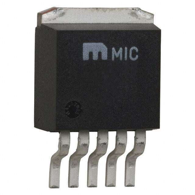
ICGOO电子元器件商城为您提供XRP6272ITC5TR-F由Exar设计生产,在icgoo商城现货销售,并且可以通过原厂、代理商等渠道进行代购。 XRP6272ITC5TR-F价格参考。ExarXRP6272ITC5TR-F封装/规格:PMIC - 稳压器 - 线性, Linear Voltage Regulator IC Positive Fixed or Adjustable 1 Output 5V, Adjustable 2A TO-252-5。您可以下载XRP6272ITC5TR-F参考资料、Datasheet数据手册功能说明书,资料中有XRP6272ITC5TR-F 详细功能的应用电路图电压和使用方法及教程。
| 参数 | 数值 |
| 产品目录 | 集成电路 (IC)半导体 |
| 描述 | IC REG LDO 5V/ADJ 2A TO252-5低压差稳压器 2A LDO LOW NOISE 5V AND ADJ OUTPUT |
| 产品分类 | |
| 品牌 | Exar Corporation |
| 产品手册 | |
| 产品图片 |
|
| rohs | 符合RoHS无铅 / 符合限制有害物质指令(RoHS)规范要求 |
| 产品系列 | 电源管理 IC,低压差稳压器,Exar XRP6272ITC5TR-F- |
| 数据手册 | http://www.exar.com/Common/Content/Document.ashx?id=20803 |
| 产品型号 | XRP6272ITC5TR-F |
| 产品种类 | 低压差稳压器 |
| 供应商器件封装 | TO-252-5 |
| 其它名称 | 1016-1745-1 |
| 包装 | 剪切带 (CT) |
| 商标 | Exar |
| 回动电压—最大值 | 1.8 V |
| 安装类型 | 表面贴装 |
| 安装风格 | SMD/SMT |
| 封装 | Reel |
| 封装/外壳 | TO-252-6,DPak(5 引线 + 接片) |
| 封装/箱体 | TO-252 |
| 工作温度 | -40°C ~ 85°C |
| 工厂包装数量 | 2000 |
| 最大工作温度 | + 85 C |
| 最大输入电压 | 6 V |
| 标准包装 | 1 |
| 电压-跌落(典型值) | 0.48V @ 2A |
| 电压-输入 | 1.8 V ~ 6 V |
| 电压-输出 | 5V,可调式 |
| 电压调节准确度 | 2 % |
| 电流-输出 | 2A |
| 电流-限制(最小值) | 2.2A |
| 稳压器拓扑 | 正,固定式或可调式 |
| 稳压器数 | 1 |
| 负载调节 | 15 mV |
| 输出电压 | 5 V |
| 输出电流 | 2 A |
| 输出类型 | Adjustable |





- 商务部:美国ITC正式对集成电路等产品启动337调查
- 曝三星4nm工艺存在良率问题 高通将骁龙8 Gen1或转产台积电
- 太阳诱电将投资9.5亿元在常州建新厂生产MLCC 预计2023年完工
- 英特尔发布欧洲新工厂建设计划 深化IDM 2.0 战略
- 台积电先进制程称霸业界 有大客户加持明年业绩稳了
- 达到5530亿美元!SIA预计今年全球半导体销售额将创下新高
- 英特尔拟将自动驾驶子公司Mobileye上市 估值或超500亿美元
- 三星加码芯片和SET,合并消费电子和移动部门,撤换高东真等 CEO
- 三星电子宣布重大人事变动 还合并消费电子和移动部门
- 海关总署:前11个月进口集成电路产品价值2.52万亿元 增长14.8%

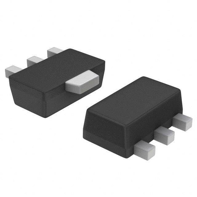

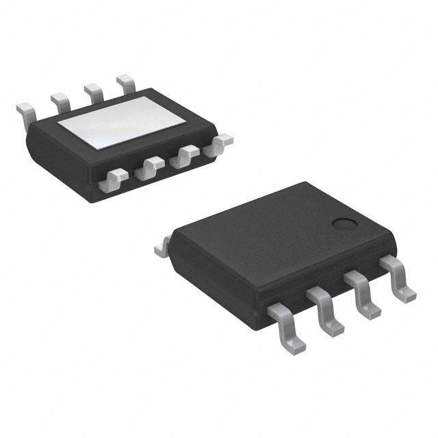


PDF Datasheet 数据手册内容提取
XXRRPP66227722 22AA 55VV--AAddjjuussttaabbllee LLooww DDrrooppoouutt VVoollttaaggee RReegguullaattoorr November 2011 Rev. 1.2.0 GENERAL DESCRIPTION APPLICATIONS The XRP6272 is a low dropout voltage Networking Equipments regulator capable of a constant output current RF Circuitry Power Supplies up to 2 Amps. A wide 1.8V to 6V input voltage range allows for single supply operations from Set-top box Equipments industry standard 1.8V, 2.8V, 3.3V, and 5V Portable Equipments power rails as well as the 5.8V rail. With better than ±2% output voltage FEATURES accuracy, low output noise and high Power Supply Rejection Ratio (PSRR), the XRP6272 is Guaranteed 2A Output Current perfectly suited for powering RF circuitries. Low 550mV Dropout at 3.3V/2A Optimized for use with small low cost ESR ceramic output capacitors and featuring a low 1.8V to 6V Single Input Voltage Range 30µA quiescent current, this device is also Fixed 5V and Adjustable Output Voltage adequate for use in battery powered portable ±2% Output Voltage Accuracy equipments. The XRP6272 operates by default as a 5V fixed output voltage regulator while 30µA Quiescent Current usage of an external resistors divider allows Power Good and Enable Functions adjustable out voltages as low as 0.7V. An Enable function, Power Good flag and output 70dB Power Supply Rejection Ratio noise reduction pin complete the feature set. Low Output Noise Built-in current limit and thermal protections 0.01µA Shutdown Current insure safe operations under abnormal operating conditions. Current Limit and Thermal Protection The XRP6272 is offered in RoHS compliant, RoHS compliant “Green”/Halogen Free “green”/halogen free 5-pin TO-252 and 8-pin 5-pin TO-252 and 8-pin Exposed pad exposed pad SOIC packages. SOIC Packages TYPICAL APPLICATION DIAGRAM Fig. 1: XRP6272 Application Diagram Exar Corporation www.exar.com 48720 Kato Road, Fremont CA 94538, USA Tel. +1 510 668-7000 – Fax. +1 510 668-7001
XXRRPP66227722 22AA 55VV--AAddjjuussttaabbllee LLooww DDrrooppoouutt VVoollttaaggee RReegguullaattoorr ABSOLUTE MAXIMUM RATINGS OPERATING RATINGS These are stress ratings only and functional operation of Input Voltage Range V ................................. 1.8V to 6V IN the device at these ratings or any other above those Operating Temperature Range ................... -40°C to 85°C indicated in the operation sections of the specifications Thermal Resistance below is not implied. Exposure to absolute maximum θ (5-Pin TO-252) .........................................100°C/W rating conditions for extended periods of time may affect JA reliability. θJC (5-Pin TO-252) ............................................ 8°C/W θ (8-pin HSOIC) ........................................... 60°C/W V , EN, BP .......................................................... 7.0V JA IN θ (8-pin HSOIC) ........................................... 15°C/W Storage Temperature .............................. -65°C to 150°C JC Power Dissipation ................................ Internally Limited Lead Temperature (Soldering, 10 sec) ................... 260°C Junction Temperature .......................................... 150°C ESD Rating (HBM - Human Body Model) .................... 2kV ESD Rating (MM - Machine Model) ........................... 500V ELECTRICAL SPECIFICATIONS Specifications with standard type are for an Operating Junction Temperature of T = 25°C only. Minimum and Maximum J limits are guaranteed through test, design, or statistical correlation. Typical values represent the most likely parametric norm at T = 25°C, and are provided for reference purposes only. Unless otherwise indicated, V = V + 1V, C = 4.7µF, J IN OUT IN C = 4.7µF or 10µF (Note 1), C = 22nF, T = 25°C. OUT BYP J Parameter Min. Typ. Max. Units Conditions Input Voltage 1.8 6.0 V Output Voltage Tolerance -2 +2 % IOUT = 1mA Continuous Output Current 2 A VIN (cid:3410) 2.3V Ground Current 30 50 µA VEN (cid:3410) 1.6V, No Load 30 50 VEN (cid:3410) 1.6V, IOUT = 300mA Standby Current 0.01 0.5 µA VEN = 0 Line Regulation 3 15 mV VIN = VOUT + 1V to 6V, IOUT =1mA Load Regulation 5 15 mV IOUT =1mA to 2A Output Current Limit 2.2 3.0 3.9 A Current Fold Back 1.0 A 960 IOUT = 2A, VOUT =1.2V Dropout Voltage (Note 2) 700 900 mV IOUT = 2A, VOUT =1.8V 550 700 IOUT = 2A, VOUT =3.3V 480 600 IOUT = 2A, VOUT =5.0V Reference Voltage Tolerance 0.686 0.7 0.714 V ADJ Pin Current 10 100 nA VADJ = VREF ADJ Pin Threshold 0.05 0.1 0.2 V Enable Turn-On Threshold 1.6 V Output ON Enable Turn-Off Threshold 0.4 V Output OFF Shutdown Pin Current 0 0.5 µA VEN = 0 Shutdown Exit Delay Time 100 µs Max Output Discharge Resistance 20 100 Ω to GND during Shutdown PGOOD Rise Threshold 90 93 % PGOOD Hysteresis 3 10 % PGOOD Delay 0.5 5 ms PGOOD Sink Capability 0.2 0.4 V IPGOOD = 10mA Ripple Rejection 70 dB f=1KHz, Ripple=0.5Vp-p Output Noise Voltage 24 µVrms CBP = 22nF, f=10Hz ~100KHz Temperature Coefficient 50 ppm/ᵒC Thermal Shutdown Temperature 150 ᵒC VIN = VOUT + 1V Thermal Shutdown Hysteresis 20 ᵒC © 2011 Exar Corporation 2/13 Rev. 1.2.0
XXRRPP66227722 22AA 55VV--AAddjjuussttaabbllee LLooww DDrrooppoouutt VVoollttaaggee RReegguullaattoorr Note 1: In the case of V ≤ 1.8V, C = 10μF is recommended. OUT OUT Note 2: Dropout Voltage is defined as input voltage minus output voltage when the output voltage drops by 1% of its nominal value at V = V + 1V. IN OUT Note 3: V is the higher value of (V + Dropout Voltage) or 1.8V. IN (min) OUT BLOCK DIAGRAM Fig. 2: XRP6272 Block Diagram PIN ASSIGNMENT Fig. 3: XRP6272 Pin Assignment © 2011 Exar Corporation 3/13 Rev. 1.2.0
XXRRPP66227722 22AA 55VV--AAddjjuussttaabbllee LLooww DDrrooppoouutt VVoollttaaggee RReegguullaattoorr PIN DESCRIPTION Name SOIC-8 TO-252 Description Enable Pin. EN 1 1 Minimum 1.6V to enable the device. Maximum 0.4V to shutdown the device. Power Input Pin. VIN 2 2 Must be closely decoupled to GND pin with a 4.7μF or greater ceramic capacitor. VOUT 3 4 Regulator Output pin. Adjustable Pin. ADJ 4 5 Output Voltage can be set by external feedback resistors when using a resistive divider. Or, connect ADJ to GND for VOUT = 5V, set by internal feedback resistors. GND 5, 8 3 Ground Signal Bypass pin. BP 6 - Connect a 22nF capacitor to GND to reduce output noise. Bypass pin can be left floating if not necessary. PGOOD 7 - Power Good open Drain Output. GND Exposed Pad Tab Connect to GND. ORDERING INFORMATION Temperature Part Number Marking Package Packing Quantity Note 1 Note 2 Range EXAR 5-pin RoHS Compliant XRP6272ITC5TR-F -40°C≤T ≤+85°C XRP6272ITC5 2K/Tape & Reel A TO-252 Halogen Free YYWWF X XRP6272I 8-pin RoHS Compliant XRP6272IDBTR-F -40°C≤T ≤+85°C YYWWF 2.5K/Tape & Reel A HSOIC Halogen Free XXXX “YY” = Year – “WW” = Work Week – “X” = Lot Number; when applicable. © 2011 Exar Corporation 4/13 Rev. 1.2.0
XXRRPP66227722 22AA 55VV--AAddjjuussttaabbllee LLooww DDrrooppoouutt VVoollttaaggee RReegguullaattoorr TYPICAL PERFORMANCE CHARACTERISTICS All data taken at V = V + 1V, T = T = 25°C, C = 4.7µF, C = 4.7µF or 10µF (Note 1) unless otherwise specified. IN OUT J A IN OUT Fig. 4: GND Current vs. VIN at VOUT=1.8V, No Load Fig. 5: GND Current vs. VIN at VOUT=3.3V, No Load Fig. 6: GND Current vs. VIN at VOUT=1.8V, 300mA Fig. 7: GND Current vs. VIN at VOUT=3.3V, 300mA Fig. 8: GND Current vs. Temp. at VOUT=1.8V, No Load Fig. 9: GND Current vs. Temp. at VOUT=3.3V, No Load © 2011 Exar Corporation 5/13 Rev. 1.2.0
XXRRPP66227722 22AA 55VV--AAddjjuussttaabbllee LLooww DDrrooppoouutt VVoollttaaggee RReegguullaattoorr Fig. 10: Dropout Voltage at VOUT = 1.8V Fig. 11: Dropout Voltage at VOUT = 3.3V Fig. 12: Dropout Voltage at VOUT = 5.0V Fig. 13: Load Transient Response at VOUT=1.8V, VIN=2.8V Fig. 14: Load Transient Response at VOUT=3.3V, VIN=4.3V Fig. 15: Load Transient Response at VOUT=5V, VIN=6V © 2011 Exar Corporation 6/13 Rev. 1.2.0
XXRRPP66227722 22AA 55VV--AAddjjuussttaabbllee LLooww DDrrooppoouutt VVoollttaaggee RReegguullaattoorr Fig. 16: Enable Startup at VOUT = 1.8V Fig. 17: Shutdown at VOUT = 1.8V Fig. 18: Enable Startup at VOUT = 5V Fig. 19: Shutdown at VOUT = 5V Fig. 20: Current Foldback at VOUT = 1.8V Fig. 21: Current Foldback at VOUT = 3.3V © 2011 Exar Corporation 7/13 Rev. 1.2.0
XXRRPP66227722 22AA 55VV--AAddjjuussttaabbllee LLooww DDrrooppoouutt VVoollttaaggee RReegguullaattoorr Fig. 22: PSRR Curve APPLICATION INFORMATION an output ceramic capacitor of at least 4.7µF or 10µF (for V ≤ 1.8V) is recommended. An The XRP6272 is a low-dropout voltage OUT input capacitor of 4.7µF is recommended. regulator with low quiescent current, low noise and high PSRR. It can support load current up X5R or X7R ceramic capacitors are to 2A. It incorporates current-limit and recommended as they have the best thermal protection features. temperature and voltage characteristics. TYPICAL APPLICATION SCHEMATIC NOISE BYPASS CAPACITOR A 22nF bypass capacitor at BP pin can reduce output voltage noise. This pin can be left floating if it is unnecessary. THEORY OF OPERATION SHUTDOWN By connecting EN pin to GND, the XRP6272 PROGRAMMING THE OUTPUT VOLTAGE can be shutdown to reduce the supply current XRP6272’s internal feedback resistors set the to 0.01μA (typ.). In this mode, the output output voltage VOUT to 5V when the ADJ pin is voltage of XRP6272 is equal to 0V. connected to GND. Alternatively; the output voltage is adjustable via the external feedback CURRENT LIMIT resistor network R1 and R2 by calculating the The XRP6272 includes current limit protection following formula: feature, which monitors and controls the maximum output current. If the output is R1 (cid:1848) (cid:3404) (cid:1848) (cid:3400)(cid:3436)1(cid:3397) (cid:3440) overloaded or shorted to ground, this can (cid:3016)(cid:3022)(cid:3021) (cid:3019)(cid:3006)(cid:3007) R2 protect the device from being damaged. where, V is the reference voltage set REF internally at 0.7V nominal. THERMAL PROTECTION INPUT & OUTPUT CAPACITORS The XRP6272 includes a thermal protection feature that protects the IC by turning off the XRP6272 is optimized for use with ceramic pass transistor when the maximum junction capacitors. To ensure stability of the device, temperature T exceeds 150ºC. J © 2011 Exar Corporation 8/13 Rev. 1.2.0
XXRRPP66227722 22AA 55VV--AAddjjuussttaabbllee LLooww DDrrooppoouutt VVoollttaaggee RReegguullaattoorr POWER DISSIPATION (cid:1842)(cid:3005)(cid:4666)(cid:3014)(cid:3002)(cid:3025)(cid:4667) (cid:3404) (cid:4666)(cid:1846)(cid:3011)(cid:4666)(cid:3014)(cid:3002)(cid:3025)(cid:4667)(cid:3398)(cid:4666)(cid:1846)(cid:3002)(cid:4667)(cid:4667)⁄ (cid:2016)(cid:3011)(cid:3002) The power dissipation across the device can be where, T is the maximum junction calculated as: J(MAX) temperature, T is the ambient temperature A (cid:1842) (cid:3404) (cid:1835) (cid:3400) (cid:4666)(cid:1848) - (cid:1848) (cid:4667) and Θ is the thermal resistance between (cid:3005) (cid:3016)(cid:3022)(cid:3021) (cid:3010)(cid:3015) (cid:3016)(cid:3022)(cid:3021) JA junction to ambient. In order to insure the The total junction temperature is calculated best thermal flow, proper mounting of the IC as: is required. (cid:1846) (cid:3404) (cid:1846) (cid:3397)(cid:1842) (cid:3400) (cid:2016) (cid:3011) (cid:3002) (cid:3005) (cid:3011)(cid:3002) LAYOUT CONSIDERATION where, T is the junction temperature, T is the J A ambient temperature and Θ is the thermal 1. Connect the bottom-side pad to a large JA resistance between junction to ambient. ground plane for good thermal conductivity and to reduce the thermal resistance of the There is a temperature rise associated with device. this power dissipated while operating in a given ambient temperature. If the calculated 2. The input capacitor C and output capacitor IN junction temperature exceeds maximum C must be placed as close as possible to OUT junction temperature specification, then the the pins V and V respectively. IN OUT built-in thermal protection feature is triggered as described previously. 3. Use short wires to connect the power supply To insure reliable performance, the maximum to pins VIN and GND on the board. allowable power dissipation for a given ambient temperature must be considered and it can be calculated as follows: © 2011 Exar Corporation 9/13 Rev. 1.2.0
XXRRPP66227722 22AA 55VV--AAddjjuussttaabbllee LLooww DDrrooppoouutt VVoollttaaggee RReegguullaattoorr TYPICAL APPLICATIONS APPLICATION 1 Fig. 23: 5V to 3.3V / 2A APPLICATION 2 Fig. 24: 5.8V to 5V RF Stage Low Noise Power Supply APPLICATION 3 Fig. 25: 2.7V Min to 1.8V / 2A Power Supply © 2011 Exar Corporation 10/13 Rev. 1.2.0
XXRRPP66227722 22AA 55VV--AAddjjuussttaabbllee LLooww DDrrooppoouutt VVoollttaaggee RReegguullaattoorr PACKAGE SPECIFICATION TO-252-5L © 2011 Exar Corporation 11/13 Rev. 1.2.0
XXRRPP66227722 22AA 55VV--AAddjjuussttaabbllee LLooww DDrrooppoouutt VVoollttaaggee RReegguullaattoorr EXPOSED PAD 8-PIN SOIC © 2011 Exar Corporation 12/13 Rev. 1.2.0
XXRRPP66227722 22AA 55VV--AAddjjuussttaabbllee LLooww DDrrooppoouutt VVoollttaaggee RReegguullaattoorr REVISION HISTORY Revision Date Description 1.1.0 10/14/2011 Initial release of Data Sheet 1.2.0 11/30/2011 Corrected pin assignment package drawing FOR FURTHER ASSISTANCE Email: customersupport@exar.com Exar Technical Documentation: http://www.exar.com/TechDoc/default.aspx? EXAR CORPORATION HEADQUARTERS AND SALES OFFICES 48720 Kato Road Fremont, CA 94538 – USA Tel.: +1 (510) 668-7000 Fax: +1 (510) 668-7030 www.exar.com NOTICE EXAR Corporation reserves the right to make changes to the products contained in this publication in order to improve design, performance or reliability. EXAR Corporation assumes no responsibility for the use of any circuits described herein, conveys no license under any patent or other right, and makes no representation that the circuits are free of patent infringement. Charts and schedules contained here in are only for illustration purposes and may vary depending upon a user’s specific application. While the information in this publication has been carefully checked; no responsibility, however, is assumed for inaccuracies. EXAR Corporation does not recommend the use of any of its products in life support applications where the failure or malfunction of the product can reasonably be expected to cause failure of the life support system or to significantly affect its safety or effectiveness. Products are not authorized for use in such applications unless EXAR Corporation receives, in writing, assurances to its satisfaction that: (a) the risk of injury or damage has been minimized; (b) the user assumes all such risks; (c) potential liability of EXAR Corporation is adequately protected under the circumstances. Reproduction, in part or whole, without the prior written consent of EXAR Corporation is prohibited. © 2011 Exar Corporation 13/13 Rev. 1.2.0
Mouser Electronics Authorized Distributor Click to View Pricing, Inventory, Delivery & Lifecycle Information: E xar: XRP6272IDBTR-F XRP6272ITC5TR-F
 Datasheet下载

