ICGOO在线商城 > 集成电路(IC) > PMIC - 稳压器 - 线性 > XC6504A121MR-G
 Datasheet下载
- 型号: XC6504A121MR-G
- 制造商: TOREX SEMICONDUCTOR
- 库位|库存: xxxx|xxxx
- 要求:
| 数量阶梯 | 香港交货 | 国内含税 |
| +xxxx | $xxxx | ¥xxxx |
查看当月历史价格
查看今年历史价格
XC6504A121MR-G产品简介:
ICGOO电子元器件商城为您提供XC6504A121MR-G由TOREX SEMICONDUCTOR设计生产,在icgoo商城现货销售,并且可以通过原厂、代理商等渠道进行代购。 XC6504A121MR-G价格参考¥1.96-¥5.90。TOREX SEMICONDUCTORXC6504A121MR-G封装/规格:PMIC - 稳压器 - 线性, Linear Voltage Regulator IC Positive Fixed 1 Output 1.2V 150mA SOT-25-5。您可以下载XC6504A121MR-G参考资料、Datasheet数据手册功能说明书,资料中有XC6504A121MR-G 详细功能的应用电路图电压和使用方法及教程。
| 参数 | 数值 |
| 产品目录 | 集成电路 (IC) |
| 描述 | IC REG LDO 1.2V 0.15A SOT25 |
| 产品分类 | |
| 品牌 | Torex Semiconductor Ltd |
| 数据手册 | |
| 产品图片 | |
| 产品型号 | XC6504A121MR-G |
| rohs | 无铅 / 符合限制有害物质指令(RoHS)规范要求 |
| 产品系列 | - |
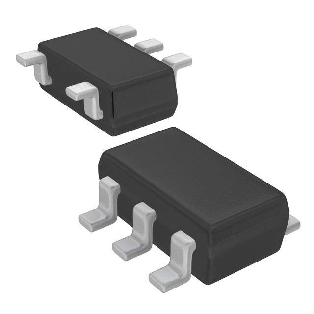
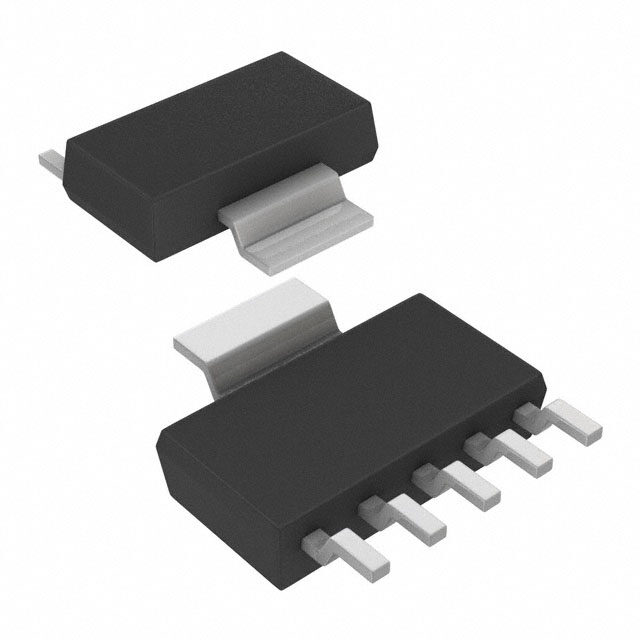
| 供应商器件封装 | SOT-25-5 |
| 其它名称 | 893-1202-1 |
| 包装 | 剪切带 (CT) |
| 安装类型 | 表面贴装 |
| 封装/外壳 | SC-74A,SOT-753 |
| 工作温度 | -40°C ~ 85°C |
| 标准包装 | 1 |
| 特色产品 | http://www.digikey.cn/product-highlights/zh/xc6504-series-small-voltage-regulators/50786 |
| 电压-跌落(典型值) | 1.41V @ 150mA |
| 电压-输入 | 最高 6V |
| 电压-输出 | 1.2V |
| 电流-输出 | 150mA |
| 电流-限制(最小值) | 150mA |
| 稳压器拓扑 | 正,固定式 |
| 稳压器数 | 1 |


- 商务部:美国ITC正式对集成电路等产品启动337调查
- 曝三星4nm工艺存在良率问题 高通将骁龙8 Gen1或转产台积电
- 太阳诱电将投资9.5亿元在常州建新厂生产MLCC 预计2023年完工
- 英特尔发布欧洲新工厂建设计划 深化IDM 2.0 战略
- 台积电先进制程称霸业界 有大客户加持明年业绩稳了
- 达到5530亿美元!SIA预计今年全球半导体销售额将创下新高
- 英特尔拟将自动驾驶子公司Mobileye上市 估值或超500亿美元
- 三星加码芯片和SET,合并消费电子和移动部门,撤换高东真等 CEO
- 三星电子宣布重大人事变动 还合并消费电子和移动部门
- 海关总署:前11个月进口集成电路产品价值2.52万亿元 增长14.8%


PDF Datasheet 数据手册内容提取
XC6504 Series ETR0347-007 0.6μA Ultra Low Power Consumption Small Voltage Regulator (C Capacitor-Less) L ■ GENERAL DESCRIPTION The XC6504 series is a highly accurate CMOS voltage regulator that achieves very low supply current operation of 0.6μA. Even output current is 1μA (when light load), the XC6504 can provide high accurate outputs, which is ideally suited for the applications to draw less output current. The usage of super small package USPN-4B02 (0.75 x 0.95mm) and the advantage of capacitor-less stable operation can contribute the board space saving outstandingly. The IC consists of a reference voltage source, an error amplifier, a driver transistor, over-current protection circuit, and a phase compensation circuit. The device is compatible with a low ESR ceramic output capacitor CL. Moreover, the device can provide stable output even without a CL output capacitor because of the excellent internal phase compensation. Output voltage is fixed internally by laser trimming technology and can be selectable in 0.1V increments within the range of 1.1V to 5.0V. The CE function enables the device to be put into standby mode by inputting a low level signal to the CE pin thereby reducing current consumption to less than 0.1μA. In the standby mode, if a CL output capacitor is used, the electric charge stored at CL can be discharged via the internal switch and as a result, the VOUT pin quickly returns to the VSS level. ■ FEATURES ■ APPLICATIONS Supply Current : 0.6μA ● Mobile devices / terminals Input Voltage Range : 1.4V~6.0V ● Wireless LAN Output Voltage Range : 1.1V~5.0V (0.1V increments) ● Modules (wireless, cameras, etc.) Output Accuracy : ±0.02V@V <2.0V OUT ±1%@V ≧2.0V OUT Temperature Stability : ±50ppm/℃ Maximum Output Current : 150mA Low On Resistance : 3.3Ω@V =3.0V OUT Standby Current : 0.01μA Protection Current : Current Limiter Shot Circuit Protection CE Function : CL Auto Discharge ON/OFF Logic=Enable High Output Capacitor : Low ESR Ceramic Capacitor (C Capacitor-Less Compatible) L Operating Ambient Temperature : -40℃~+85℃ Packages : USPN-4B02 SSOT-24 SOT-25 USPQ-4B04 Environmentally Friendly : EU RoHS Compliant, Pb Free ■ TYPICAL A PPLICATION CIRCUIT ■TYPICAL PERFORMANCE CHARACTERISTICS V =V CE IN XC6504x181xR I =0mA OUT C =C=open IN L 1.4 1.2 Ta=-40℃ A] Ta=25℃ μ 1.0 Ta=85℃ [SS t: I 0.8 n e urr 0.6 C y ppl 0.4 u S 0.2 0.0 0 1 2 3 4 5 6 Input Voltage: V [V] IN 1/33
XC6504 Series ■BLOCK DIAGRAM XC6504 Series, Type A * Diodes inside the circuits are ESD protection diodes and parasitic diodes. ■PRODUCT CLASSIFICATION ●Ordering Information XC6504①②③④⑤⑥-⑦ DESIGNATOR ITEM SYMBOL DESCRIPTION ① Type A Refer to Selection Guide ②③ Output Voltage 11~50 e.g. 1.8V → ②=1, ③=8 ④ Output Voltage Accuracy 1 ±0.02V (VOUT<2.0V), ±1% (VOUT≧2.0V) 7R-G USPN-4B02 (5,000pcs/Reel) NR-G SSOT-24 (3,000pcs/Reel) ⑤⑥-⑦(*1) Packages (Order Unit) MR-G SOT-25 (3,000pcs/Reel) 9R-G USPQ-4B04 (3,000pcs/Reel) (*1) The “-G” suffix denotes Halogen and Antimony free as well as being fully EU RoHS compliant. ●Selection Guide CE PULL-DOWN TYPE CURRENT LIMITTER RESISTOR CL AUTO-DISCHARGE A Yes No Yes 2/33
XC6504 Series ■PIN CONFIGURATION *The dissipation pad for the USPQ-4B04 package should be solder-plated in reference mount pattern and metal masking so as to enhance mounting strength and heat release. If the pad needs to be connected to other pins, it should be connected to the V (No. 2) pin. SS ■PIN ASSIGNMENT PIN NUMBER PIN NAME FUNCTIONS USPN-4B02 USPQ-4B04 SSOT-24 SOT-25 1 1 3 5 V Output OUT 2 2 2 2 V Ground SS 3 3 1 3 CE ON/OFF Control 4 4 4 1 V Power Supply Input IN - - - 4 NC No Connection ■FUNCTION CHART PIN NAME SIGNAL STATUS L Stand-by CE H Active OPEN Unstable * Please avoid the state of OPEN, and connect CE pin to any arbitrary voltage. 3/33
XC6504 Series ■ABSOLUTE MAXIMUM RATINGS Ta=25℃ PARAMETER SYMBOL RATINGS UNITS Input Voltage VIN -0.3~+6.5 V Output Current IOUT 470 (*1) mA Output Voltage VOUT -0.3~VIN+0.3 or +6.5 (*2) V CE Input Voltage VCE -0.3~+6.5 V 100 USPQ-4B04 550 (40mm x 40mm Standard board) (*3) 100 USPN-4B02 550 (40mm x 40mm Standard board) (*3) Power Dissipation Pd mW 150 SSOT-24 500 (40mm x 40mm Standard board) (*3) 250 SOT-25 600 (40mm x 40mm Standard board) (*3) Operating Ambient Temperature Topr -40~+85 ℃ Storage Temperature Tstg -55~+125 ℃ All voltages are described based on the V . SS (*1) Please use within the range of I ≦Pd / (V -V ) OUT IN OUT (*2) The maximum rating corresponds to the lowest value between V +0.3 or +6.5. IN (*3) The power dissipation figure shown is PCB mounted and is for reference only Please see the power dissipation page for the mounting condition. . 4/33
XC6504 Series ■ELECTRICAL CHARACTERISTICS Ta=25℃ PARAMETER SYMBOL CONDITIONS MIN. TYP. MAX. UNITS CIRCUIT Input Voltage V I =1μA 1.4 - 6.0 V ① IN OUT V <2.0V -0.02 +0.02 Output Voltage V (*1) OUT(T) V (*2) V ① OUT(E) VOUT(T)≧2.0V ×0.99 OUT(T) ×1.01 Maximum Output Current I 150 - - mA ① OUTMAX 1μA≦I ≦1mA - 3 16 OUT Load Regulation ∆V mV ① OUT 1mA≦I ≦150mA - 17 50 OUT Vdif1 (*3) I =50mA - E-1 (*4) OUT Dropout Voltage V ① Vdif2 (*3) I =150mA - E-2 (*4) OUT V <1.9V - 0.60 1.27 OUT(T) Supply Current I I =0mA 1.9V≦V <4.0V - 0.65 1.50 μA ② SS OUT OUT(T) V ≧4.0V - 0.80 1.80 OUT(T) Stand-by Current I V =6.0V, V =V - 0.01 0.10 μA ② STB IN CE SS I =1μA V +0.5V≦V ≦6.0V - 0.01 0.13 OUT OUT(T) IN V <1.2V, ∆V / OUT(T) Line Regulation OUT 1.7V≦V ≦6.0V %/V ① (∆VIN・VOUT) IOUT=1mA V ≧I1N.2V, - 0.01 0.19 OUT(T) V +0.5V≦V ≦6.0V OUT(T) IN Output Voltage ∆V / I =10mA, Temperature OUT OUT - ±50 - ppm/℃ ① (∆Topr ・V ) -40℃≦Topr≦85℃ Characteristics OUT Current Limit I V =V ×0.95 150 270 - mA ① LIM OUT OUT(E) Short-Circuit Current I V =V - 80 - mA ① SHORT OUT SS C Auto-Discharge L R V =V , V =V 280 450 640 Ω ① Resistance DCHG CE SS OUT OUT(T) CE "H" Level Voltage V 0.91 - 6.00 V ③ CEH CE "L" Level Voltage V V - 0.38 V ③ CEL SS CE "H" Level Current I V = 6.0V -0.1 - 0.1 μA ③ CEH IN CE "L" Level Current I V =6.0V, V =V -0.1 - 0.1 μA ③ CEL IN CE SS NOTE: Unless otherwise stated, V =V , I =1mA, C =C=open, V is below: CE IN OUT IN L IN V <2.5V : V =3.5V OUT(T) IN V ≧2.5V : V =V +1.0V OUT(T) IN OUT(T) (*1) V is Effective output voltage OUT(E) (*2) V is Nominal output voltage OUT(T) (*3) Vdif={V -V } IN1 OUT1 V is the input voltage when V appears at the V pin while input voltage is gradually decreased. IN1 OUT1 OUT VOUT1 is the voltage equal to 98% of the normal output voltage when amply stabilized VOUT(T) +1.0V is input at the VIN pin. (*4) E-1 / E-2: DROPOUT VOLTAGE (Refer to the Voltage Chart) 5/33
XC6504 Series ■ELECTRICAL CHARACTERISTICS (Continued) Voltage Chart Ta=25℃ NOMINAL - E-1 E-2 OUTPUT OUTPUT VOLTAGE DROPOUT VOLTAGE VOLTAGE (V) (V) VOUT(T) VOUT(E) Vdif1 Vdif2 (V) MIN. MAX. TYP. MAX. TYP. MAX. 1.1 1.0800 1.1200 0.96 1.35 1.51 2.05 1.2 1.1800 1.2200 0.87 1.23 1.41 1.93 1.3 1.2800 1.3200 0.77 1.12 1.33 1.83 1.4 1.3800 1.4200 0.69 1.01 1.24 1.72 1.5 1.4800 1.5200 0.62 0.91 1.17 1.63 1.6 1.5800 1.6200 0.56 0.84 1.10 1.54 1.7 1.6800 1.7200 0.51 0.77 1.04 1.47 1.8 1.7800 1.8200 0.47 0.72 0.99 1.40 1.9 1.8800 1.9200 0.42 0.64 0.92 1.29 2.0 1.9800 2.0200 0.37 0.58 0.86 1.20 2.1 2.0790 2.1210 2.2 2.1780 2.2220 0.31 0.47 0.75 1.05 2.3 2.2770 2.3230 2.4 2.3760 2.4240 0.26 0.40 0.67 0.92 2.5 2.4750 2.5250 2.6 2.5740 2.6260 0.23 0.34 0.60 0.82 2.7 2.6730 2.7270 2.8 2.7720 2.8280 0.20 0.30 0.54 0.74 2.9 2.8710 2.9290 3.0 2.9700 3.0300 3.1 3.0690 3.1310 3.2 3.1680 3.2320 0.17 0.26 0.50 0.67 3.3 3.2670 3.3330 3.4 3.3660 3.4340 3.5 3.4650 3.5350 3.6 3.5640 3.6360 3.7 3.6630 3.7370 0.15 0.22 0.43 0.59 3.8 3.7620 3.8380 3.9 3.8610 3.9390 4.0 3.9600 4.0400 4.1 4.0590 4.1410 4.2 4.1580 4.2420 0.13 0.19 0.38 0.51 4.3 4.2570 4.3430 4.4 4.3560 4.4440 4.5 4.4550 4.5450 4.6 4.5540 4.6460 4.7 4.6530 4.7470 0.11 0.17 0.35 0.47 4.8 4.7520 4.8480 4.9 4.8510 4.9490 5.0 4.9500 5.0500 0.10 0.16 0.32 0.43 6/33
XC6504 Series ■TEST CIRCUITS Circuit ① Circuit ② Circuit ③ 7/33
XC6504 Series ■ OPERATIONAL EXPLANATION The voltage divided by resistors R1 & R2 is compared with the internal reference voltage by the error amplifier. The VOUT pin is then driven by the subsequent output signal. The output voltage at the VOUT pin is controlled and stabilized by a system of negative feedback. XC6504 Series, Type A <Current Limiter, Short-Circuit Protection> The XC6504 series includes a combination of a fixed current limiter circuit & a foldback circuit, which aid the operations of the current limiter and circuit protection. When the load current reaches the current limit level, the fixed current limiter circuit operates and output voltage drops. As a result of this drop in output voltage, the foldback circuit operates, output voltage drops further and output current decreases. <CE Pin> The XC6504 internal circuitry can be shutdown via the signal from the CE pin with the XC6504 series. In shutdown mode with CE low level voltage is input, output at the VOUT pin will be pulled down to the VSS level via parallel to R1 & R2 and CL discharge resistance (RDCHG). If this IC is used with the correct output voltage for the CE pin, the logic is fixed and the IC will operate normally. However, supply current may increase as a result of through current in the IC's internal circuitry when medium voltage is input. The output voltage becomes unstable when the CE pin is opened. <CL Auto-Discharge Function> The XC6504 series can quickly discharge the electric charge at the output capacitor (CL), when a low signal to the CE pin, which enables a whole IC circuit put into OFF state, is inputted via an internal switch located between the VOUT pin and the VSS pin. In this state, the application is protected from a glitch operation caused by the electric charge at the output capacitor (CL). Moreover, discharge time of the output capacitor (CL) is set by the CL auto-discharge resistance (RDCHG) and the output capacitor (CL). By setting time constant of a CL auto-discharge resistance value (RDCHG) and an output capacitor value (CL) as τ(τ= CL x RDCHG), the output voltage after discharge via the internal switch is calculated by the following formulas. Please also note RDCHG is depended on VIN and When VIN is high, RDCHG is low. V = VOUT(E)×e-t/τ or t=τln(VOUT(E) / V) V: Output voltage after discharge VOUT(E): Output voltage t: Discharge time τ: CL x RDCHG <Low ESR Capacitors> The XC6504 series can provide a stable output voltage even if without CL capacitor or with a low ESR CL capacitor because of a built-in phase compensation circuit. In case of adding a CL capacitor, we suggest that an output capacitor (CL) is connected as close as possible to the VOUT pin and the VSS pin. When VIN stabilization is needed, please place an input capacitor (CIN) as close as to the VIN pin and the VSS pin. 8/33
XC6504 Series ■NOTES ON USE 1. For temporary, transitional voltage drop or voltage rising phenomenon, the IC is liable to malfunction should the ratings be exceeded. 2. Where wiring impedance is high, operations may become unstable due to noise and/or phase lag depending on output current. Please keep the resistance low between VIN and VSS wiring in particular. 3. Please wire the input capacitor (CIN) and the output capacitor (CL) as close to the IC as possible. 4. Capacitances of these capacitors (CIN, CL) are decreased by the influences of bias voltage and ambient temperature. Care shall be taken for capacitor selection to ensure stability of phase compensation from the point of ESR influence. 5. Torex places an importance on improving our products and their reliability. We request that users incorporate fail-safe designs and post-aging prevention treatment when using Torex products in their systems. 9/33
XC6504 Series ■TYPICAL PERFORMANCE CHARACTERISTICS Unless otherwise stated, Ta=25℃, V =V , I =1mA, C =C=open, V is below. CE IN OUT IN L IN V <2.5V : V =3.5V OUT(T) IN V ≧2.5V : V =V +1.0V OUT(T) IN OUT(T) (1) Output Voltage vs. Output Current XC6504x121xR XC6504x121xR 1.4 1.4 1.2 1.2 V] V] [T 1.0 [T 1.0 VOU VIN=2.5V VOU Ta=-40℃ e: 0.8 VIN=3.5V e: 0.8 g g Ta=25℃ olta 0.6 VIN=4.5V olta 0.6 Ta=85℃ utput V 0.4 VIN=6.0V utput V 0.4 O O 0.2 0.2 0.0 0.0 0 50 100 150 200 250 300 350 400 0 50 100 150 200 250 300 350 400 Output Current: I [mA] Output Current: I [mA] OUT OUT XC6504x181xR XC6504x181xR 2.1 2.1 1.8 1.8 V] V] [UT 1.5 [UT 1.5 O VIN=2.5V O V V Ta=-40℃ e: 1.2 VIN=3.5V e: 1.2 g g Ta=25℃ a VIN=4.5V a Volt 0.9 VIN=6.0V Volt 0.9 Ta=85℃ put 0.6 put 0.6 ut ut O O 0.3 0.3 0.0 0.0 0 50 100 150 200 250 300 350 400 0 50 100 150 200 250 300 350 400 Output Current: I [mA] Output Current: I [mA] OUT OUT XC6504x281xR XC6504x281xR 3.2 3.2 2.8 2.8 V] V] V [OUT 22..04 VVIINN==33..58VV V [OUT 22..04 Ta=-40℃ age: 1.6 VIN=4.5V age: 1.6 Ta=25℃ Volt 1.2 VIN=6.0V Volt 1.2 Ta=85℃ ut ut Outp 0.8 Outp 0.8 0.4 0.4 0.0 0.0 0 50 100 150 200 250 300 350 400 0 50 100 150 200 250 300 350 400 Output Current: I [mA] Output Current: I [mA] OUT OUT 10/33
XC6504 Series ■TYPICAL PERFORMANCE CHARACTERISTICS (Continued) Unless otherwise stated, Ta=25℃, V =V , I =1mA, C =C=open, V is below. CE IN OUT IN L IN V <2.5V : V =3.5V OUT(T) IN V ≧2.5V : V =V +1.0V OUT(T) IN OUT(T) (1) Output Voltage vs. Output Current XC6504x421xR XC6504x421xR 4.9 4.9 4.2 4.2 V] V] [T 3.5 [T 3.5 VOU VIN=4.5V VOU Ta=-40℃ ge: 2.8 VIN=5.2V ge: 2.8 Ta=25℃ a a olt 2.1 VIN=6.0V olt 2.1 Ta=85℃ V V utput 1.4 utput 1.4 O O 0.7 0.7 0.0 0.0 0 50 100 150 200 250 300 350 400 0 50 100 150 200 250 300 350 400 Output Current: I [mA] Output Current: I [mA] OUT OUT (2) Output Voltage vs. Input Voltage XC6504x121xR XC6504x121xR 1.4 1.300 1.2 V] V] 1.250 [UT 1.0 [UT O O e: V 0.8 e: V 1.200 g g a a Volt 0.6 IOUT=1μA Volt 1.150 IOUT=1μA Output 00..24 IIOOUUTT==11m0mAA Output 1.100 IIIOOOUUUTTT===111m00m0AmAA IOUT=100mA 0.0 1.050 0 1 2 3 4 5 6 2.5 3 3.5 4 4.5 5 5.5 6 Input Voltage: V [V] Input Voltage: V [V] IN IN XC6504x181xR XC6504x181xR 2.1 1.900 1.8 V] V] 1.850 [T 1.5 [T U U O O V V 1.800 e: 1.2 e: g g a a Volt 0.9 IOUT=1μA Volt 1.750 IOUT=1μA Output 00..36 IIIOOOUUUTTT===1110m00mAmAA Output 1.700 IIIOOOUUUTTT===111m00m0AmAA 0.0 1.650 0 1 2 3 4 5 6 3 3.5 4 4.5 5 5.5 6 Input Voltage: VIN [V] Input Voltage: VIN [V] 11/33
XC6504 Series ■TYPICAL PERFORMANCE CHARACTERISTICS (Continued) Unless otherwise stated, Ta=25℃, V =V , I =1mA, C =C=open, V is below. CE IN OUT IN L IN V <2.5V : V =3.5V OUT(T) IN V ≧2.5V : V =V +1.0V OUT(T) IN OUT(T) (2) Output Voltage vs. Input Voltage XC6504x281xR XC6504x281xR 3.2 2.900 2.8 V] V] 2.850 [T 2.4 [T U U VO 2.0 VO 2.800 e: e: ag 1.6 ag Output Volt 01..82 IIIOOOUUUTTT===111μm0mAAA Output Volt 22..770500 IIIOOOUUUTTT===111μm0mAAA 0.4 IOUT=100mA IOUT=100mA 0.0 2.650 0 1 2 3 4 5 6 3.5 4 4.5 5 5.5 6 Input Voltage: VIN [V] Input Voltage: VIN [V] XC6504x421xR XC6504x421xR 4.9 4.300 4.2 V] V] 4.250 [T 3.5 [T OU OU V V 4.200 e: 2.8 e: g g Volta 2.1 IOUT=1μA Volta 4.150 IOUT=1μA put 1.4 IOUT=1mA put IOUT=1mA Out 0.7 IOUT=10mA Out 4.100 IOUT=10mA IOUT=100mA IOUT=100mA 0.0 4.050 0 1 2 3 4 5 6 5 5.2 5.4 5.6 5.8 6 Input Voltage: V [V] Input Voltage: V [V] IN IN (3) Dropout Voltage vs. Output Current XC6504x121xR XC6504x181xR 1800 1800 1600 Ta=-40℃ 1600 mV] 1400 Ta=25℃ mV] 1400 Ta=-40℃ dif [ 1200 Ta=85℃ dif [ 1200 Ta=25℃ e: V 1000 e: V 1000 Ta=85℃ ag ag Volt 800 Volt 800 ut 600 ut 600 o o Drop 400 ※ Below the minimum operating Voltage Drop 400 200 200 0 0 0 50 100 150 0 50 100 150 Output Current: I [mA] Output Current: I [mA] OUT OUT 12/33
XC6504 Series ■TYPICAL PERFORMANCE CHARACTERISTICS (Continued) Unless otherwise stated, Ta=25℃, V =V , I =1mA, C =C=open, V is below. CE IN OUT IN L IN V <2.5V : V =3.5V OUT(T) IN V ≧2.5V : V =V +1.0V OUT(T) IN OUT(T) (3) Dropout Voltage vs. Output Current XC6504x281xR XC6504x421xR 800 800 700 700 V] V] m 600 Ta=-40℃ m 600 Ta=-40℃ e: Vdif [ 500 TTaa==2855℃℃ e: Vdif [ 500 TTaa==2855℃℃ ag 400 ag 400 olt olt ut V 300 ut V 300 po 200 po 200 o o Dr Dr 100 100 0 0 0 50 100 150 0 50 100 150 Output Current: I [mA] Output Current: I [mA] OUT OUT (4) Supply Current vs. Input Voltage XC6504x121xR XC6504x181xR 1.4 IOUT=0mA 1.4 IOUT=0mA 1.2 Ta=-40℃ 1.2 Ta=-40℃ A] Ta=25℃ A] Ta=25℃ μ μ [S 1.0 Ta=85℃ [S 1.0 Ta=85℃ nt: IS 0.8 nt: IS 0.8 e e Curr 0.6 Curr 0.6 ply 0.4 ply 0.4 p p Su Su 0.2 0.2 0.0 0.0 0 1 2 3 4 5 6 0 1 2 3 4 5 6 Input Voltage: V [V] Input Voltage: V [V] IN IN XC6504x281xR XC6504x421xR 1.4 IOUT=0mA 1.4 IOUT=0mA 1.2 Ta=-40℃ 1.2 A] Ta=25℃ A] μ μ 1.0 Ta=85℃ 1.0 [SS [SS nt: I 0.8 nt: I 0.8 e e urr 0.6 urr 0.6 C C ply 0.4 ply 0.4 up up Ta=-40℃ S 0.2 S 0.2 Ta=25℃ Ta=85℃ 0.0 0.0 0 1 2 3 4 5 6 0 1 2 3 4 5 6 Input Voltage: VIN [V] Input Voltage: VIN [V] 13/33
XC6504 Series ■TYPICAL PERFORMANCE CHARACTERISTICS (Continued) Unless otherwise stated, Ta=25℃, V =V , I =1mA, C =C=open, V is below. CE IN OUT IN L IN V <2.5V : V =3.5V OUT(T) IN V ≧2.5V : V =V +1.0V OUT(T) IN OUT(T) (5) Supply Current vs. Output Current XC6504x121xR XC6504x181xR 50 VIN=3.5V 50 VIN=3.5V Ta=-40℃ Ta=-40℃ 40 Ta=25℃ 40 Ta=25℃ A] Ta=85℃ A] Ta=85℃ μ μ S [ S [ S30 S30 nt: I nt: I e e Curr20 Curr20 y y pl pl p p Su10 Su10 0 0 0 30 60 90 120 150 0 30 60 90 120 150 Output Current: IOUT [mA] Output Current: IOUT [mA] XC6504x281xR XC6504x421xR 50 VIN=3.8V 50 VIN=5.2V Ta=-40℃ Ta=-40℃ A]40 Ta=25℃ A]40 Ta=25℃ μ Ta=85℃ μ Ta=85℃ S [ S [ S30 S30 nt: I nt: I e e Curr20 Curr20 y y pl pl p p Su10 Su10 0 0 0 30 60 90 120 150 0 30 60 90 120 150 Output Current: IOUT [mA] Output Current: IOUT [mA] 14/33
XC6504 Series ■TYPICAL PERFORMANCE CHARACTERISTICS (Continued) Unless otherwise stated, Ta=25℃, V =V , I =1mA, C =C=open, V is below. CE IN OUT IN L IN V <2.5V : V =3.5V OUT(T) IN V ≧2.5V : V =V +1.0V OUT(T) IN OUT(T) ((65)) Output Voltage vs. Ambient Temperature XC6504x121xR XC6504x181xR 1.30 1.90 V] V] [T 1.25 [T 1.85 OU OU V V e: e: ag 1.20 ag 1.80 olt olt ut V IOUT=1μA ut V IOUT=1μA Outp 1.15 IIOOUUTT==110mmAA Outp 1.75 IIOOUUTT==11m0mAA IOUT=100mA IOUT=100mA 1.10 1.70 -50 -25 0 25 50 75 100 -50 -25 0 25 50 75 100 Ambient Temperature: Ta [℃] Ambient Temperature: Ta [℃] XC6504x281xR XC6504x421xR 2.90 4.30 [V]UT 2.85 [V]UT 4.25 O O V V e: e: ag 2.80 ag 4.20 olt olt utput V 2.75 IIIOOOUUUTTT===1110μmmAAA utput V 4.15 IIOOUUTT==11mμAA O O IOUT=10mA IOUT=100mA IOUT=100mA 2.70 4.10 -50 -25 0 25 50 75 100 -50 -25 0 25 50 75 100 Ambient Temperature: Ta [℃] Ambient Temperature: Ta [℃] ((76)) Supply Current vs. Ambient Temperature ((87)) CE Threshold Voltage vs. Ambient Temperature XC6504xxx1xR XC6504xxx1xR I =0mA OUT 1.4 1.0 VOUT=1.2V μA] 1.21 VVOOUUTT==12..88VV V [V]CE 0.8 nt: I [SS 0.8 VOUT=4.2V oltage: 0.6 e V Curr 0.6 old 0.4 Supply 00..24 E Thresh 0.2 CCEE""HL""LLEEVVEELL C 0 0.0 -50 -25 0 25 50 75 100 -50 -25 0 25 50 75 100 Ambient Temperature: Ta [℃] Ambient Temperature: Ta [℃] 15/33
XC6504 Series ■TYPICAL PERFORMANCE CHARACTERISTICS (Continued) Unless otherwise stated, Ta=25℃, V =V , I =1mA, C =C=open, V is below. CE IN OUT IN L IN V <2.5V : V =3.5V OUT(T) IN V ≧2.5V : V =V +1.0V OUT(T) IN OUT(T) ((98)) Rising Response Time XC6504x121xR XC6504x181xR V =0V→3.5V , tr=5μs V =0V→3.5V , tr=5μs 6.0 IN 4.0 6.0 IN 4.0 4.0 3.5 4.0 3.5 2.0 Input Voltage 3.0 V] 2.0 Input Voltage 3.0 V] V [V]IN 0.0 IOUT=1μA 2.5 V [OUT V [V]IN 0.0 2.5 V [OUT e: IOUT=1mA e: e: Output Voltage e: ag -2.0 IOUT=10mA 2.0 ag ag -2.0 2.0 ag olt IOUT=100mA olt olt olt V -4.0 1.5 V V -4.0 1.5 V ut ut ut ut p p p IOUT=1μA p In -6.0 Output Voltage 1.0 Out In -6.0 IOUT=1mA 1.0 Out -8.0 0.5 -8.0 IOUT=10mA 0.5 IOUT=100mA -10.0 0.0 -10.0 0.0 Time (100μs/div) Time (100μs/div) XC6504x281xR XC6504x421xR 6.0 VIN=0V→3.8V , tr=5μs 8.0 6.0 VIN=0V→5.2V , tr=5μs 8.0 4.0 7.0 4.0 Input Voltage 7.0 Input Voltage: V [V]IN ---64202.....00000 IOnupIIIIOOOOtuptUUUUu VTTTTt o====Vl1111toaμm00ltgm0AaeAmAgAe 23456.....00000 Output Voltage: V [V]OUT Input Voltage: V [V]IN ---64202.....00000 OutIIOOpuUUtTT V==o11lμmtaAgAe 23456.....00000 Output Voltage: V [V]OUT IOUT=10mA -8.0 1.0 -8.0 1.0 IOUT=100mA -10.0 0.0 -10.0 0.0 Time (100μs/div) Time (100μs/div) (1(90)) Input Transient Response XC6504x121xR XC6504x121xR 5.0 VIN=3.5V⇔4.5V , tr=tf=5μs 3.5 5.0 VIN=3.5V⇔4.5V , tr=tf=5μs 3.5 4.0 Input Voltage 3.0 4.0 Input Voltage 3.0 V [V]IN 3.0 IOUT=1μA 2.5 V [V]OUT V [V]IN 3.0 2.5 V [V]OUT e: IOUT=1mA e: e: without CL e: ut Voltag 12..00 IIOOUUTT==1100m0mAA 12..50 ut Voltag ut Voltag 12..00 CL=0.1μF(ceramic) 12..50 ut Voltag Inp 0.0 1.0 Outp Inp 0.0 1.0 Outp Output Voltage Output Voltage -1.0 0.5 -1.0 0.5 Time (100μs/div) Time (100μs/div) 16/33
XC6504 Series ■TYPICAL PERFORMANCE CHARACTERISTICS (Continued) Unless otherwise stated, Ta=25℃, V =V , I =1mA, C =C=open, V is below. CE IN OUT IN L IN V <2.5V : V =3.5V OUT(T) IN V ≧2.5V : V =V +1.0V OUT(T) IN OUT(T) ((190) ) Input Transient Response XC6504x181xR XC6504x181xR VIN=3.5V⇔4.5V , tr=tf=5μs VIN=3.5V⇔4.5V , tr=tf=5μs 5.0 4.0 5.0 4.0 4.0 Input Voltage 3.5 4.0 Input Voltage 3.5 V] V] e: V [V]IN 3.0 IIOOUUTT==11μmAA 3.0 e: V [OUT e: V [V]IN 3.0 wCiLt=h0o.u1tμ CFL(ceramic) 3.0 e: V [OUT ag 2.0 IOUT=10mA 2.5 ag ag 2.0 2.5 ag Volt IOUT=100mA Volt Volt Volt ut 1.0 2.0 ut ut 1.0 2.0 ut p p p p In Out In Out 0.0 1.5 0.0 1.5 Output Voltage Output Voltage -1.0 1.0 -1.0 1.0 Time (100μs/div) Time (100μs/div) XC6504x281xR XC6504x281xR 5.0 VIN=3.8V⇔4.8V , tr=tf=5μs 5.0 5.0 VIN=3.8V⇔4.8V , tr=tf=5μs 5.0 4.0 Input Voltage 4.5 4.0 Input Voltage 4.5 V] V] Voltage: V [V]IN 23..00 IIIIOOOOUUUUTTTT====1111μm00m0AAmAA 34..50 Voltage: V [OUT Voltage: V [V]IN 23..00 wCiLt=h0o.u1tμ CFL(ceramic) 34..50 Voltage: V [OUT Input 1.0 3.0 Output Input 1.0 3.0 Output 0.0 Output Voltage 2.5 0.0 Output Voltage 2.5 -1.0 2.0 -1.0 2.0 Time (100μs/div) Time (100μs/div) XC6504x421xR XC6504x421xR V =5.2V⇔6.0V , tr=tf=5μs V =5.2V⇔6.0V , tr=tf=5μs 7.0 IN 6.5 7.0 IN 6.5 Input Voltage Input Voltage 6.0 6.0 6.0 6.0 V] V] V [V]IN 5.0 IOUT=1μA 5.5 V [OUT V [V]IN 5.0 5.5 V [OUT Voltage: 4.0 IIIOOOUUUTTT===111m00m0AmAA 5.0 Voltage: Voltage: 4.0 wCiLt=h0o.u1tμ CFL(ceramic) 5.0 Voltage: Input 3.0 4.5 Output Input 3.0 4.5 Output 2.0 4.0 2.0 4.0 Output Voltage Output Voltage 1.0 3.5 1.0 3.5 Time (100μs/div) Time (100μs/div) 17/33
XC6504 Series ■TYPICAL PERFORMANCE CHARACTERISTICS (Continued) Unless otherwise stated, Ta=25℃, V =V , I =1mA, C =C=open, V is below. CE IN OUT IN L IN V <2.5V : V =3.5V OUT(T) IN V ≧2.5V : V =V +1.0V OUT(T) IN OUT(T) ((1110)) Load Transient Response XC6504x121xR XC6504x121xR IOUT=1μA⇔10mA , tr=tf=5μs IOUT=10mA⇔30mA , tr=tf=5μs 3 50 3 150 V] 2 Output Voltage 40A] V] 2 Output Voltage 120A] [OUT [mUT [OUT [mUT age: V 1 30ent: IO age: V 1 90 ent: IO Volt 0 20Curr Volt 0 60 Curr Output -1 Output Current 10Output Output -1 Output Current 30 Output -2 0 -2 0 Time (200μs/div) Time (200μs/div) XC6504x121xR XC6504x121xR I =1mA⇔10mA , tr=tf=5μs I =1mA⇔10mA , tr=tf=5μs OUT OUT 3 50 3 50 V] 2 Output Voltage 40A] V] 2 Output Voltage 40A] [OUT [mUT [OUT [mUT V 1 30 O V 1 30 O ge: nt: I ge: without CL nt: I Volta 0 20Curre Volta 0 CCLL==01..10μμFF 20Curre Output -1 Output Current 10Output Output -1 Output Current 10Output -2 0 -2 0 Time (200μs/div) Time (200μs/div) XC6504x181xR XC6504x181xR I =1μA⇔10mA , tr=tf=5μs I =10mA⇔30mA , tr=tf=5μs 3 OUT 50 3 OUT 150 Output Voltage Output Voltage V] 2 40A] V] 2 120A] V [OUT 1 30 [mOUT V [OUT 1 90 [mOUT ge: nt: I ge: nt: I a e a e Volt 0 20Curr Volt 0 60 Curr Output -1 Output Current 10Output Output -1 Output Current 30 Output -2 0 -2 0 Time (200μs/div) Time (200μs/div) 18/33
XC6504 Series ■TYPICAL PERFORMANCE CHARACTERISTICS (Continued) Unless otherwise stated, Ta=25℃, V =V , I =1mA, C =C=open, V is below. CE IN OUT IN L IN V <2.5V : V =3.5V OUT(T) IN V ≧2.5V : V =V +1.0V OUT(T) IN OUT(T) ((1110)) Load Transient Response XC6504x181xR XC6504x181xR 3 IOUT=1mA⇔10mA , tr=tf=5μs 50 3 IOUT=1mA⇔10mA , tr=tf=5μs 50 Output Voltage Output Voltage V] 2 40A] V] 2 40A] [OUT [mUT [OUT [mUT age: V 1 30ent: IO age: V 1 wCiLt=h0o.u1tμ CFL 30ent: IO Volt 0 20Curr Volt 0 CL=1.0μF 20Curr Output -1 Output Current 10Output Output -1 Output Current 10Output -2 0 -2 0 Time (200μs/div) Time (200μs/div) XC6504x281xR XC6504x281xR I =1μA⇔10mA , tr=tf=5μs I =10mA⇔30mA , tr=tf=5μs OUT OUT 4 50 4 150 Output Voltage Output Voltage V] 3 40A] V] 3 120A] V [OUT 2 30 [mOUT V [OUT 2 90 [mOUT ge: nt: I ge: nt: I a e a e Volt 1 20Curr Volt 1 60 Curr Output 0 Output Current 10Output Output 0 Output Current 30 Output -1 0 -1 0 Time (200μs/div) Time (200μs/div) XC6504x281xR XC6504x281xR IOUT=1mA⇔10mA , tr=tf=5μs IOUT=1mA⇔10mA , tr=tf=5μs 4 50 4 50 Output Voltage Output Voltage V] 3 40A] V] 3 40A] V [OUT 2 30 [mOUT V [OUT 2 without CL 30 [mOUT ge: nt: I ge: CL=0.1μF nt: I Volta 1 20Curre Volta 1 CL=1.0μF 20Curre Output 0 Output Current 10Output Output 0 Output Current 10Output -1 0 -1 0 Time (200μs/div) Time (200μs/div) 19/33
XC6504 Series ■TYPICAL PERFORMANCE CHARACTERISTICS (Continued) Unless otherwise stated, Ta=25℃, V =V , I =1mA, C =C=open, V is below. CE IN OUT IN L IN V <2.5V : V =3.5V OUT(T) IN V ≧2.5V : V =V +1.0V OUT(T) IN OUT(T) ((1110)) Load Transient Response XC6504x421xR XC6504x421xR 6 IOUT=1μA⇔10mA , tr=tf=5μs 50 6 IOUT=10mA⇔30mA , tr=tf=5μs 150 age: V [V]OUT 45 Output Voltage 3400ent: I [mA]OUT age: V [V]OUT 45 Output Voltage 91020ent: I [mA]OUT Volt 3 20Curr Volt 3 60 Curr Output 2 Output Current 10Output Output 2 Output Current 30 Output 1 0 1 0 Time (200μs/div) Time (200μs/div) XC6504x421xR XC6504x421xR I =1mA⇔10mA , tr=tf=5μs I =1mA⇔10mA , tr=tf=5μs OUT OUT 6 50 6 50 V] 5 40A] V] 5 40A] V [OUT 4 Output Voltage 30 [mOUT V [OUT 4 Output Voltage 30 [mOUT ge: nt: I ge: without CL nt: I a e a e Volt 3 20Curr Volt 3 CCLL==01..10μμFF 20Curr Output 2 Output Current 10Output Output 2 Output Current 10Output 1 0 1 0 Time (200μs/div) Time (200μs/div) ((1121)) CE Rising Response Time XC6504x121xR XC6504x181xR V =0V→V , tr=5μs V =0V→V , tr=5μs 4.0 CE IN 3.0 4.0 CE IN 3.0 CE Input Voltage CE Input Voltage 2.0 2.5 2.0 2.5 V [V]CE 0.0 IIOOUUTT==11μmAA 2.0 [V]OUT V [V]CE 0.0 2.0 [V]OUT Voltage: -2.0 IIOOUUTT==1100m0mAA 1.5 oltage: V Voltage: -2.0 Output Voltage 1.5 oltage: V CE Input --64..00 Output Voltage 01..50 Output V CE Input --64..00 IIIOOOUUUTTT===111μm0mAAA 01..50 Output V IOUT=100mA -8.0 0.0 -8.0 0.0 Time (100μs/div) Time (100μs/div) 20/33
XC6504 Series ■TYPICAL PERFORMANCE CHARACTERISTICS (Continued) Unless otherwise stated, Ta=25℃, V =V , I =1mA, C =C=open, V is below. CE IN OUT IN L IN V <2.5V : V =3.5V OUT(T) IN V ≧2.5V : V =V +1.0V OUT(T) IN OUT(T) ((1121)) CE Rising Response Time XC6504x281xR XC6504x421xR V =0V→V , tr=5μs V =0V→V , tr=5μs 6.0 CE IN 6.0 6.0 CE IN 6.0 CE Input Voltage 4.0 5.0 4.0 CE Input Voltage 5.0 V] V] V] V] V [CE 2.0 4.0 [OUT V [CE 2.0 4.0 [OUT put Voltage: -20..00 Output Voltage 23..00 ut Voltage: V put Voltage: -20..00 Output Voltage 23..00 ut Voltage: V n IOUT=1μA p n IOUT=1μA p CE I IOUT=1mA Out CE I IOUT=1mA Out -4.0 1.0 -4.0 1.0 IOUT=10mA IOUT=10mA IOUT=100mA IOUT=100mA -6.0 0.0 -6.0 0.0 Time (100μs/div) Time (100μs/div) ((1132)) Power Supply Rejection Ratio XC6504x121xR XC6504x121xR V =3.5V+0.5V V =3.5V+0.5V IN P-PAC IN P-PAC 100 100 o: 90 IOUT=1μA o: 90 without CL Rejection RatiR [dB] 56780000 IIIOOOUUUTTT===111m00m0AmAA Rejection RatiR [dB] 56780000 CCLL==01..10μμFF((cceerraammiicc)) y R y R pplPS 40 pplPS 40 Su 30 Su 30 wer 20 wer 20 o o P 10 P 10 0 0 10 100 1k 10k 100k 1M 10 100 1k 10k 100k 1M Frequency: f [Hz] Frequency: f [Hz] XC6504x181xR XC6504x181xR 100 VIN=3.5V+0.5VP-PAC 100 VIN=3.5V+0.5VP-PAC 90 IOUT=1μA 90 without CL o: o: ati 80 IOUT=1mA ati 80 CL=0.1μF(ceramic) n R 70 IOUT=10mA n R 70 CL=1.0μF(ceramic) ctioB] 60 IOUT=100mA ctioB] 60 RejeR [d 50 RejeR [d 50 pply PSR 40 pply PSR 40 Su 30 Su 30 er 20 er 20 w w o o P 10 P 10 0 0 10 100 1k 10k 100k 1M 10 100 1k 10k 100k 1M Frequency: f [Hz] Frequency: f [Hz] 21/33
XC6504 Series ■TYPICAL PERFORMANCE CHARACTERISTICS (Continued) Unless otherwise stated, Ta=25℃, V =V , I =1mA, C =C=open, V is below. CE IN OUT IN L IN V <2.5V : V =3.5V OUT(T) IN V ≧2.5V : V =V +1.0V OUT(T) IN OUT(T) ((1132)) Power Supply Rejection Ratio XC6504x281xR XC6504x281xR VIN=3.8V+0.5VP-PAC VIN=3.8V+0.5VP-PAC 100 100 atio: 8900 IIOOUUTT==11μmAA atio: 8900 wCiLt=h0o.u1tμ CFL(ceramic) n R 70 IOUT=10mA n R 70 CL=1.0μF(ceramic) ctioB] 60 IOUT=100mA ctioB] 60 RejeR [d 50 RejeR [d 50 y R y R pplPS 40 pplPS 40 Su 30 Su 30 er 20 er 20 w w o o P 10 P 10 0 0 10 100 1k 10k 100k 1M 10 100 1k 10k 100k 1M Frequency: f [Hz] Frequency: f [Hz] XC6504x421xR XC6504x421xR VIN=5.2V+0.5VP-PAC VIN=5.2V+0.5VP-PAC 100 100 90 IOUT=1μA 90 without CL Ratio: 80 IIOOUUTT==11m0mAA Ratio: 80 CL=0.1μF(ceramic) n 70 n 70 CL=1.0μF(ceramic) o IOUT=100mA o y RejectiRR [dB] 5600 y RejectiRR [dB] 5600 pplPS 40 pplPS 40 er Su 2300 er Su 2300 w w o o P 10 P 10 0 0 10 100 1k 10k 100k 1M 10 100 1k 10k 100k 1M Frequency: f [Hz] Frequency: f [Hz] 22/33
XC6504 Series ■PACKAGING INFORMATION ●USPQ-4B04 Reference Pattern Layout ●USPQ-4B04 Reference Metal Mask Design 23/33
XC6504 Series ■PACKAGING INFORMATION (Continued) ●USPN-4B02 (unit:mm) 0.75±0.05 1pinINDENT 0.18±0.05 1 2 4 3 (0.4) ●●UUSSPPNN--44BB0022 R参efe考reパnceタ Pーattンernレ Laイyoアut ウト (unit:mm) ●USPN-4B02 Reference Metal Mask Design ●USPN-4B02 参考メタルマスクデザイン (unit:mm) 0.23 0.23 0.18 0.18 C0.12 0.14 0.4 0.14 0.115 0.4 0.115 24/33
XC6504 Series ■PACKAGING INFORMATION (Continued) 25/33
XC6504 Series ■PACKAGING INFORMATION (Continued) 26/33
XC6504 Series ■PACKAGING INFORMATION (Continued) ●USPN-4B02 Power Dissipation (40mm x 40mm Standard board) Power dissipation data for the USPN-4B02 is shown in this page. The value of power dissipation varies with the mount board conditions. Please use this data as the reference data taken in the following condition. 1. Measurement Condition Condition: Mount on a board Ambient: Natural convection Soldering: Lead (Pb) free Board: Dimensions 40 x 40 mm (1600 mm2 in one side) Copper (Cu) traces occupy 50% of the front and 50% of the back. The copper area is divided into four block, one block is 12.5% of total. The USPN-4 package has for terminals. Each terminal connects one copper block in the front and one in the back. Material: Glass Epoxy (FR-4) Thickness: 1.6 mm Through-hole: 4 x 0.4 Diameter Evaluation Board (Unit:mm) 2.Power Dissipation vs. Ambient Temperature Board Mount (Tj max = 125℃) Ambient Temperature(℃) Power Dissipation Pd(mW) Thermal Resistance (℃/W) 25 550 181.82 85 220 Pd vs Ta 600 ) W 500 m ( d 400 P n o ati 300 p si s Di 200 r e w o 100 P 0 25 45 65 85 105 125 Ambient Temperature(℃) 27/33
XC6504 Series ■PACKAGING INFORMATION (Continued) ●SSOT-24 Power Dissipation(40mm x 40mm Standard board) Power dissipation data for the SSOT-24 is shown in this page. The value of power dissipation varies with the mount board conditions. Please use this data as the reference data taken in the following condition. 1. Measurement Condition Condition: Mount on a board Ambient: Natural convection Soldering: Lead (Pb) free Board: Dimensions 40 x 40 mm (1600 mm2 in one side) Copper (Cu) traces occupy 50% of the board area In top and back faces Package heat-sink is tied to the copper traces Material: Glass Epoxy (FR-4) Thickness: 1.6mm Through-hole: 4 x 0.8 Diameter Evaluation Board (Unit:mm) 2.Power Dissipation vs. Ambient Temperature Board Mount (Tj max = 125℃) Ambient Temperature(℃) Power Dissipation Pd(mW) Thermal Resistance (℃/W) 25 500 200.00 85 200 Pd vs Ta 600 ) W 500 m ( d P 400 n o pati 300 si s Di 200 r e w o 100 P 0 25 45 65 85 105 125 Ambient Temperature(℃) 28/33
XC6504 Series ■PACKAGING INFORMATION (Continued) ●SOT-25 Power Dissipation (40mm x 40mm Standard board) Power dissipation data for the SOT-25 is shown in this page. The value of power dissipation varies with the mount board conditions. Please use this data as the reference data taken in the following condition. 1. Measurement Condition Condition: Mount on a board Ambient: Natural convection Soldering: Lead (Pb) free Board: Dimensions 40 x 40 mm (1600 mm2 in one side) Copper (Cu) traces occupy 50% of the board area In top and back faces Package heat-sink is tied to the copper traces (Board of SOT-26 is used.) Material: Glass Epoxy (FR-4) Thickness: 1.6mm Through-hole: 4 x 0.8 Diameter Evaluation Board (Unit:mm) 2.Power Dissipation vs. Ambient Temperature Board Mount (Tj max = 125℃) Ambient Temperature(℃) Power Dissipation Pd(mW) Thermal Resistance (℃/W) 25 600 166.67 85 240 Pd vs Ta 700 ) 600 W m ( 500 d P n 400 o ati p si 300 s Di r 200 e w Po 100 0 25 45 65 85 105 125 Ambient Temperature(℃) 29/33
XC6504 Series ■MARKING RULE SOT-25 (Under-dot) Magnified * SOT-25 with the under-dot marking is used. ① represents products series MARK PRODUCT SERIES 9 XC6504A*****-G ② represents output voltage range MARK OUTPUT VOLTAGE OUTPUT VOLTAGE PRODUCT SERIES 1.1V~3.9V 4.0V~5.0V A B XC6504A*****-G ③ represents output voltage MARK OUTPUT VOLTAGE (V) MARK OUTPUT VOLTAGE (V) 0 - 4.00 F 2.50 - 1 1.10 4.10 H 2.60 - 2 1.20 4.20 K 2.70 - 3 1.30 4.30 L 2.80 - 4 1.40 4.40 M 2.90 - 5 1.50 4.50 N 3.00 - 6 1.60 4.60 P 3.10 - 7 1.70 4.70 R 3.20 - 8 1.80 4.80 S 3.30 - 9 1.90 4.90 T 3.40 - A 2.00 5.00 U 3.50 - B 2.10 - V 3.60 - C 2.20 - X 3.70 - D 2.30 - Y 3.80 - E 2.40 - Z 3.90 - ④,⑤ represents production lot number 01~09, 0A~0Z, 11~9Z, A1~A9, AA~AZ, B1~ZZ in order. (G, I, J, O, Q, W excluded) *No character inversion used. 30/33
XC6504 Series ■MARKING RULE (Continued) ●SSOT-24 (With the orientation bar at the bottom) ●USPQ-4B04 4 3 4 3 ② ④ ① ② ① ③ ③ ④ 1 2 1 2 * SSOT-24 with the orientation bar at the bottom is used. ① represents output voltage range MARK OUTPUT VOLTAGE OUTPUT VOLTAGE PRODUCT SERIES 1.1V~3.9V 4.0V~5.0V P R XC6504A*****-G ② represents output voltage MARK OUTPUT VOLTAGE (V) MARK OUTPUT VOLTAGE (V) 0 - 4.00 F 2.50 - 1 1.10 4.10 H 2.60 - 2 1.20 4.20 K 2.70 - 3 1.30 4.30 L 2.80 - 4 1.40 4.40 M 2.90 - 5 1.50 4.50 N 3.00 - 6 1.60 4.60 P 3.10 - 7 1.70 4.70 R 3.20 - 8 1.80 4.80 S 3.30 - 9 1.90 4.90 T 3.40 - A 2.00 5.00 U 3.50 - B 2.10 - V 3.60 - C 2.20 - X 3.70 - D 2.30 - Y 3.80 - E 2.40 - Z 3.90 - ③,④ represents production lot number 01~09, 0A~0Z, 11~9Z, A1~A9, AA~AZ, B1~ZZ in order. (G, I, J, O, Q, W excluded) *No character inversion used. 31/33
XC6504 Series ■MARKING RULE (Continued) USPN-4B02 4 3 ① ② ③ 1 2 ① represents output voltage range MARK OUTPUT VOLTAGE OUTPUT VOLTAGE PRODUCT SERIES 1.1V~3.9V 4.0V~5.0V A B XC6504A*****-G ② represents output voltage MARK OUTPUT VOLTAGE (V) MARK OUTPUT VOLTAGE (V) 0 - 4.00 F 2.50 - 1 1.10 4.10 H 2.60 - 2 1.20 4.20 K 2.70 - 3 1.30 4.30 L 2.80 - 4 1.40 4.40 M 2.90 - 5 1.50 4.50 N 3.00 - 6 1.60 4.60 P 3.10 - 7 1.70 4.70 R 3.20 - 8 1.80 4.80 S 3.30 - 9 1.90 4.90 T 3.40 - A 2.00 5.00 U 3.50 - B 2.10 - V 3.60 - C 2.20 - X 3.70 - D 2.30 - Y 3.80 - E 2.40 - Z 3.90 - ③ represents production lot number 0~9, A~Z in order. (G, I, J, O, Q, W excluded) *No character inversion used. 32/33
XC6504 Series 1. The product and product specifications contained herein are subject to change without notice to improve performance characteristics. Consult us, or our representatives before use, to confirm that the information in this datasheet is up to date. 2. The information in this datasheet is intended to illustrate the operation and characteristics of our products. We neither make warranties or representations with respect to the accuracy or completeness of the information contained in this datasheet nor grant any license to any intellectual property rights of ours or any third party concerning with the information in this datasheet. 3. Applicable export control laws and regulations should be complied and the procedures required by such laws and regulations should also be followed, when the product or any information contained in this datasheet is exported. 4. The product is neither intended nor warranted for use in equipment of systems which require extremely high levels of quality and/or reliability and/or a malfunction or failure which may cause loss of human life, bodily injury, serious property damage including but not limited to devices or equipment used in 1) nuclear facilities, 2) aerospace industry, 3) medical facilities, 4) automobile industry and other transportation industry and 5) safety devices and safety equipment to control combustions and explosions. Do not use the product for the above use unless agreed by us in writing in advance. 5. Although we make continuous efforts to improve the quality and reliability of our products; nevertheless Semiconductors are likely to fail with a certain probability. So in order to prevent personal injury and/or property damage resulting from such failure, customers are required to incorporate adequate safety measures in their designs, such as system fail safes, redundancy and fire prevention features. 6. Our products are not designed to be Radiation-resistant. 7. Please use the product listed in this datasheet within the specified ranges. 8. We assume no responsibility for damage or loss due to abnormal use. 9. All rights reserved. No part of this datasheet may be copied or reproduced unless agreed by Torex Semiconductor Ltd in writing in advance. TOREX SEMICONDUCTOR LTD. 33/33