ICGOO在线商城 > X9241AYVIZ
- 型号: X9241AYVIZ
- 制造商: Intersil
- 库位|库存: xxxx|xxxx
- 要求:
| 数量阶梯 | 香港交货 | 国内含税 |
| +xxxx | $xxxx | ¥xxxx |
查看当月历史价格
查看今年历史价格
X9241AYVIZ产品简介:
ICGOO电子元器件商城为您提供X9241AYVIZ由Intersil设计生产,在icgoo商城现货销售,并且可以通过原厂、代理商等渠道进行代购。 提供X9241AYVIZ价格参考以及IntersilX9241AYVIZ封装/规格参数等产品信息。 你可以下载X9241AYVIZ参考资料、Datasheet数据手册功能说明书, 资料中有X9241AYVIZ详细功能的应用电路图电压和使用方法及教程。
| 参数 | 数值 |
| 产品目录 | 集成电路 (IC)半导体 |
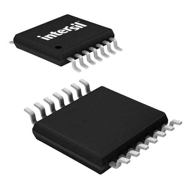
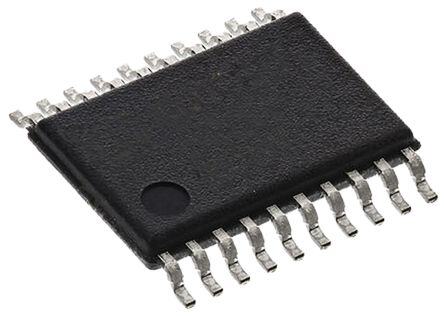
| 描述 | IC POT DGTL QUAD 20-TSSOP数字电位计 IC QD CMOS EEPOT 2KOHM S 20LD |
| 产品分类 | |
| 品牌 | Intersil |
| 产品手册 | |
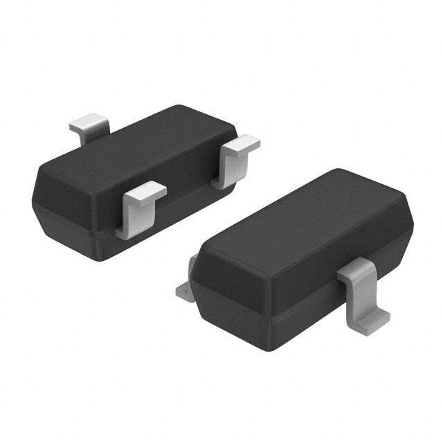
| 产品图片 |
|
| rohs | 符合RoHS无铅 / 符合限制有害物质指令(RoHS)规范要求 |
| 产品系列 | 数字电位计 IC,Intersil X9241AYVIZXDCP™ |
| 数据手册 | |
| 产品型号 | X9241AYVIZ |
| PCN组件/产地 | |
| POT数量 | Quad |
| 产品目录页面 | |
| 产品种类 | 数字电位计 IC |
| 供应商器件封装 | 20-TSSOP |
| 包装 | 管件 |
| 商标 | Intersil |
| 存储器类型 | 非易失 |
| 安装类型 | 表面贴装 |
| 封装 | Tube |
| 封装/外壳 | 20-TSSOP(0.173",4.40mm 宽) |
| 封装/箱体 | TSSOP-20 |
| 工作温度 | -40°C ~ 85°C |
| 工作电源电压 | 5 V |
| 工厂包装数量 | 75 |
| 弧刷存储器 | Non Volatile |
| 抽头 | 64 |
| 接口 | I²C(设备位址) |
| 数字接口 | Serial (2-Wire) |
| 最大工作温度 | + 85 C |
| 最小工作温度 | - 40 C |
| 标准包装 | 75 |
| 每POT分接头 | 64 |
| 温度系数 | 标准值 ±300 ppm/°C |
| 电压-电源 | 4.5 V ~ 5.5 V |
| 电源电压-最大 | 5.5 V |
| 电源电压-最小 | 4.5 V |
| 电源电流 | 3 mA |
| 电路数 | 4 |
| 电阻 | 2 KOhms |
| 电阻(Ω) | 2k |
| 系列 | X9241A |




- 商务部:美国ITC正式对集成电路等产品启动337调查
- 曝三星4nm工艺存在良率问题 高通将骁龙8 Gen1或转产台积电
- 太阳诱电将投资9.5亿元在常州建新厂生产MLCC 预计2023年完工
- 英特尔发布欧洲新工厂建设计划 深化IDM 2.0 战略
- 台积电先进制程称霸业界 有大客户加持明年业绩稳了
- 达到5530亿美元!SIA预计今年全球半导体销售额将创下新高
- 英特尔拟将自动驾驶子公司Mobileye上市 估值或超500亿美元
- 三星加码芯片和SET,合并消费电子和移动部门,撤换高东真等 CEO
- 三星电子宣布重大人事变动 还合并消费电子和移动部门
- 海关总署:前11个月进口集成电路产品价值2.52万亿元 增长14.8%


PDF Datasheet 数据手册内容提取
DATASHEET X9241A FN8164 Quad Digital Controlled Potentionmeters (XDCP™) Non-Volatile/Low Rev 7.00 Power/2-Wire/64 Taps August 17, 2015 The X9241A integrates four digitally controlled Features potentiometers (XDCP) on a monolithic CMOS integrated • Four potentiometers in one package microcircuit. • 2-wire serial interface The digitally controlled potentiometer is implemented using 63 resistive elements in a series array. Between each • Register oriented format element are tap points connected to the wiper terminal - Direct read/write/transfer of wiper positions through switches. The position of the wiper on the array is - Store as many as four positions per potentiometer controlled by the user through the 2-wire bus interface. Each • Terminal Voltages: +5V, -3.0V potentiometer has associated with it a volatile Wiper Counter Register (WCR) and 4 nonvolatile Data Registers • Cascade resistor arrays (DR0:DR3) that can be directly written to and read by the • Low power CMOS user. The contents of the WCR controls the position of the wiper on the resistor array through the switches. Power up • High Reliability recalls the contents of DR0 to the WCR. - Endurance–100,000 data changes per bit per register - Register data retention–100 years The XDCP can be used as a three-terminal potentiometer or as a two-terminal variable resistor in a wide variety of • 16-bytes of nonvolatile memory applications including control, parameter adjustments, and • 3 resistor array values signal processing. - 2k10k50kor combination - Cascadable for values of 4kto 200k • Resolution: 64 taps each pot • 20 Ld plastic DIP, 20 Ld TSSOP and 20 Ld SOIC packages • Pb-free available (RoHS compliant) Block Diagram VCC VSS R0 R1 VH0/RH0 R0 R1 VH2/ WIPER WIPER REGISTER RH2 COUNTER COUNTER REGISTER REGISTER ARRAY POT 2 R2 R3 (WCR) VL0/RL0 R2 R3 (WCR) VL2/RL2 VW0/RW0 VW2/RW2 SCL SDA INTERFACE A0 AND CONTROL A1 CIRCUITRY 8 A2 A3 DATA R0 R1 VH1/RH1 R0 R1 VH3/RH3 WIPER REGISTER WIPER REGISTER COUNTER ARRAY COUNTER ARRAY REGISTER POT 1 REGISTER POT 3 R2 R3 (WCR) VL1/RL1 R2 R3 (WCR) VL3/RL3 VW1/RW1 VW3/RW3 FN8164 Rev 7.00 Page 1 of 17 August 17, 2015
X9241A Ordering Information POTENTIOMETER VCC LIMITS ORGANIZATION TEMP RANGE PACKAGE PART NUMBER PART MARKING (V) (k) (°C) (RoHS Compliant) X9241AMPZ (Note) X9241AMPZ 5 ±10% 2/10/50 0 to +70 20 Ld PDIP*** (No longer available, Pot 0 = 2k recommended replacement: Pot 1 = 10k X9241AMSZT1) Pot 2 = 10k X9241AMPIZ (Note) X9241AMPIZ -40 to +85 20 Ld PDIP*** (No longer available, Pot 3 = 50k recommended replacement: X9241AMSZT1) X9241AMSZ* (Note) X9241AMS Z 0 to +70 20 Ld SOIC X9241AMSIZ* (Note) X9241AMSI Z -40 to +85 20 Ld SOIC X9241AMVZ (Note) X9241AM VZ 0 to +70 20 Ld TSSOP X9241AMVIZ* (Note) X9241AM VIZ -40 to +85 20 Ld TSSOP X9241AWPIZ (Note) X9241AWPIZ 10 0 to +70 20 Ld PDIP X9241AWSZ* (Note) X9241AWS Z Pot 0 = 10k 0 to +70 20 Ld SOIC X9241AWSIZ* (Note) X9241AWSI Z -40 to +85 20 Ld SOIC Pot 1 = 10k X9241AWVZ* (Note) X9241AW VZ 0 to +70 20 Ld TSSOP Pot 2 = 10k X9241AWVIZ* (Note) X9241AW VIZ -40 to +85 20 Ld TSSOP Pot 3 = 10k X9241AYPZ (Note) X9241AYPZ 2 0 to +70 20 Ld PDIP*** (No longer available, recommended Pot 0 = 2k replacement: X9241AYSIZ) Pot 1 = 2k X9241AYSZ* (Note) X9241AYS Z Pot 2 = 2k 0 to +70 20 Ld SOIC X9241AYSIZ* (Note) X9241AYSI Z -40 to +85 20 Ld SOIC Pot 3 = 2k X9241AYVZ (Note) X9241AY VZ 0 to +70 20 Ld TSSOP (No longer available, recommended replacement: X9241AYVIZ) X9241AYVIZ* (Note) X9241AY VIZ -40 to +85 20 Ld TSSOP X9241AUPZ (Note) X9241AUPZ 5 ±10% 50 0 to +70 20 Ld PDIP*** X9241AUPIZ (Note) X9241AUPIZ Pot 0 = 50k -40 to +85 20 Ld PDIP*** X9241AUSZ* (Note) X9241AUS Z 0 to +70 20 Ld SOIC Pot 1 = 50k X9241AUSIZ* (Note) X9241AUSI Z -40 to +85 20 Ld SOIC Pot 2 = 50k X9241AUVZ* (Note) X9241AU VZ 0 to +70 20 Ld TSSOP Pot 3 = 50k (No longer available, recommended replacement: X9241AUSZT1) X9241AUVIZ* (Note) X9241AU VIZ -40 to +85 20 Ld TSSOP *Add "T1" suffix for tape and reel. ***Pb-free PDIPs can be used for through hole wave solder processing only. They are not intended for use in Reflow solder processing applications. NOTE: These Intersil Pb-free plastic packaged products employ special Pb-free material sets; molding compounds/die attach materials and 100% matte tin plate PLUS ANNEAL - e3 termination finish, which is RoHS compliant and compatible with both SnPb and Pb-free soldering operations. Intersil Pb-free products are MSL classified at Pb-free peak reflow temperatures that meet or exceed the Pb-free requirements of IPC/JEDEC J STD-020. FN8164 Rev 7.00 Page 2 of 17 August 17, 2015
X9241A Pin Descriptions Pin Names Host Interface Pins SYMBOL DESCRIPTION Serial Clock (SCL) VH0/RH0 to VH3/RH3, Potentiometer Pins (terminal equivalent) VL0/RL0 to VL3/RL3 The SCL input is used to clock data into and out of the VW0/RW0 to VW3/RW3 Potentiometer Pins (wiper equivalent) X9241A. Principles of Operation Serial Data (SDA) SDA is a bidirectional pin used to transfer data into and out of The X9241A is a highly integrated microcircuit incorporating the device. It is an open drain output and may be wire-ORed four resistor arrays, their associated registers and counters with any number of open drain or open collector outputs. An and the serial interface logic providing direct communication open drain output requires the use of a pull-up resistor. For between the host and the XDCP potentiometers. selecting typical values, refer to the guidelines for calculating Serial Interface typical values on the bus pull-up resistors graph. The X9241A supports a bidirectional bus oriented protocol. Address The protocol defines any device that sends data onto the bus The Address inputs are used to set the least significant as a transmitter and the receiving device as the receiver. The 4-bits of the 8-bit slave address. A match in the slave address device controlling the transfer is a master and the device being serial data stream must be made with the Address input in controlled is the slave. The master will always initiate data order to initiate communication with the X9241A. transfers and provide the clock for both transmit and receive operations. Therefore, the X9241A will be considered a slave Potentiometer Pins device in all applications. VH/RH(VH0/RH0 TO VH3/RH3), VL/RL (VL0/RL0 TO VL3/RL3) Clock and Data Conventions The RH and RL inputs are equivalent to the terminal Data states on the SDA line can change only during SCL LOW connections on either end of a mechanical potentiometer. periods (tLOW). SDA state changes during SCL HIGH are VW/RW (VW0/RW0 TO VW3/RW3) reserved for indicating start and stop conditions. The wiper outputs are equivalent to the wiper output of a Start Condition mechanical potentiometer. All commands to the X9241A are preceded by the start condition, which is a HIGH to LOW transition of SDA while SCL Pinout is HIGH (tHIGH). The X9241A continuously monitors the SDA X9241A and SCL lines for the start condition and will not respond to any (20 LD DIP, SOIC, TSSOP) command until this condition is met. TOP VIEW Stop Condition VW0/RW0 1 20 VCC All communications must be terminated by a stop condition, VL0/RL0 2 19 VW3/RW3 which is a LOW to HIGH transition of SDA while SCL is HIGH. VH0/RH0 3 18 VL3/RL3 Acknowledge A0 4 17 VH3/RH3 Acknowledge is a software convention used to provide a A2 5 16 A1 X9241A positive handshake between the master and slave devices on VW1/RW1 6 15 A3 the bus to indicate the successful receipt of data. The VL1/RL1 7 14 SCL transmitting device, either the master or the slave, will release VH1/RH1 8 13 VW2/RW2 the SDA bus after transmitting 8-bits. The master generates a SDA 9 12 VL2/RL2 ninth clock cycle and during this period the receiver pulls the SDA line LOW to acknowledge that it successfully received the VSS 10 11 VH2/RH2 8-bits of data. See Figure 7. The X9241A will respond with an acknowledge after Pin Names recognition of a start condition and its slave address and once again after successful receipt of the command byte. If the SYMBOL DESCRIPTION command is followed by a data byte the X9241A will respond SCL Serial Clock with a final acknowledge. SDA Serial Data Array Description A0 to A3 Address The X9241A is comprised of four resistor arrays. Each array contains 63 discrete resistive segments that are connected in FN8164 Rev 7.00 Page 3 of 17 August 17, 2015
X9241A series. The physical ends of each array are equivalent to the Flow 1. ACK Polling Sequence fixed terminals of a mechanical potentiometer (VH/RH and VL/RL inputs). NONVOLATILE WRITE COMMAND COMPLETED At both ends of each array and between each resistor segment ENTER ACK POLLING is a FET switch connected to the wiper (VW/RW) output. Within each individual array only one switch may be turned on at a time. These switches are controlled by the Wiper Counter ISSUE START Register (WCR). The 6 least significant bits of the WCR are decoded to select, and enable, 1 of 64 switches. The WCR may be written directly, or it can be changed by ISSUE SLAVE ISSUE STOP transferring the contents of one of four associated Data ADDRESS Registers into the WCR. These Data Registers and the WCR can be read and written by the host system. ACK NO Device Addressing RETURNED? Following a start condition the master must output the address YES of the slave it is accessing. The most significant 4-bits of the slave address are the device type identifier (refer to Figure 1). For the X9241A, this is fixed as 0101[B]. FURTHER NO OPERATION? DEVICE TYPE YES IDENTIFIER ISSUE ISSUE STOP INSTRUCTION 0 1 0 1 A3 A2 A1 A0 DEVICE ADDRESS PROCEED PROCEED FIGURE 1. SLAVE ADDRESS Instruction Structure The next 4-bits of the slave address are the device address. The physical device address is defined by the state of the A0 to The next byte sent to the X9241A contains the instruction and A3 inputs. The X9241A compares the serial data stream with register pointer information. The 4 most significant bits are the the address input state; a successful compare of all 4 address instruction. The next 4-bits point to one of four pots and when bits is required for the X9241A to respond with an applicable they point to one of four associated registers. The acknowledge. format is in Figure 2. Acknowledge Polling POTENTIOMETER SELECT The disabling of the inputs, during the internal nonvolatile write operation, can be used to take advantage of the typical 5ms I3 I2 I1 I0 P1 P0 R1 R0 EEPROM write cycle time. Once the stop condition is issued to indicate the end of the nonvolatile write command, the X9241A initiates the internal write cycle. ACK polling can be initiated INSTRUCTIONS REGISTER SELECT immediately. This involves issuing the start condition followed by the device slave address. If the X9241A is still busy with the FIGURE 2. INSTRUCTION BYTE FORMAT write operation, no ACK will be returned. If the X9241A has completed the write operation, an ACK will be returned and the The 4 high order bits define the instruction. The next 2-bits (P1 master can then proceed with the next operation. and P0) select which one of the four potentiometers is to be affected by the instruction. The last 2-bits (R1 and R0) select one of the four registers that are to be acted upon when a register oriented instruction is issued. Four of the nine instructions end with the transmission of the instruction byte. The basic sequence is illustrated in Figure 3. These two-byte instructions exchange data between the WCR and one of the data registers. A transfer from a Data Register to a WCR is essentially a write to a static RAM. The response of FN8164 Rev 7.00 Page 4 of 17 August 17, 2015
X9241A the wiper to this action will be delayed tSTPWV. A transfer from value to the selected Data Register. The sequence of WCR current wiper position to a Data Register is a write to operations is shown in Figure 4. nonvolatile memory and takes a minimum of tWR to complete. The Increment/Decrement command is different from the other The transfer can occur between one of the four potentiometers commands. Once the command is issued and the X9241A has and one of its associated registers; or it may occur globally, responded with an acknowledge, the master can clock the wherein the transfer occurs between all four of the selected wiper up and/or down in one segment steps; thereby, potentiometers and one of their associated registers. providing a fine tuning capability to the host. For each SCL Four instructions require a three-byte sequence to complete. clock pulse (tHIGH) while SDA is HIGH, the selected wiper will These instructions transfer data between the host and the move one resistor segment towards the VH/RH terminal. X9241A; either between the host and one of the Data Similarly, for each SCL clock pulse while SDA is LOW, the Registers or directly between the host and the WCR. These selected wiper will move one resistor segment towards the instructions are: Read WCR, read the current wiper position of VL/RL terminal. A detailed illustration of the sequence and the selected pot; Write WCR, change current wiper position of timing for this operation is shown in Figures 5 and 6 the selected pot; Read Data Register, read the contents of the respectively. selected nonvolatile register; Write Data Register, write a new SCL SDA S 0 1 0 1 A3 A2 A1 A0 A I3 I2 I1 I0 P1 P0 R1 R0 A S T C C T A K K O R P T FIGURE 3. TWO-BYTE INSTRUCTION SEQUENCE SCL SDA S 0 1 0 1 A3 A2 A1 A0 A I3 I2 I1 I0 P1 P0 R1 R0 A CM DW D5 D4 D3 D2 D1 D0 A S T C C C T A K K K O R P T FIGURE 4. THREE-BYTE INSTRUCTION SEQUENCE SCL SDA X X S 0 1 0 1 A3 A2 A1 A0 A I3 I2 I1 I0 P1 P0 R1 R0 A I I I D D S T C C N N N E E T A K K C C C C C O R 1 2 n 1 n P T FIGURE 5. INCREMENT/DECREMENT INSTRUCTION SEQUENCE FN8164 Rev 7.00 Page 5 of 17 August 17, 2015
X9241A INC/DEC CMD ISSUED tCLWV SCL SDA VOLTAGE OUT VW/RW FIGURE 6. INCREMENT/DECREMENT TIMING LIMITS TABLE 1. INSTRUCTION SET INSTRUCTION FORMAT INSTRUCTION I3 I2 I1 I0 P1 P0 R1 R0 OPERATION Read WCR 1 0 0 1 1/0 1/0 X X Read the contents of the Wiper Counter Register pointed to by P1 to P0 (Note 1) (Note 2) Write WCR 1 0 1 0 1/0 1/0 X X Write new value to the Wiper Counter Register pointed to by P1 to P0 Read Data 1 0 1 1 1/0 1/0 1/0 1/0 Read the contents of the Register pointed to by P1 to P0 and R1 to R0 Register Write Data 1 1 0 0 1/0 1/0 1/0 1/0 Write new value to the Register pointed to by P1 to P0 and R1 to R0 Register XFR Data 1 1 0 1 1/0 1/0 1/0 1/0 Transfer the contents of the Register pointed to by P1 to P0 and R1 to Register to WCR R0 to its associated WCR XFR WCR to 1 1 1 0 1/0 1/0 1/0 1/0 Transfer the contents of the WCR pointed to by P1 to P0 to the Register Data Register pointed to by R1 to R0 Global XFR 0 0 0 1 X X 1/0 1/0 Transfer the contents of the Data Registers pointed to by R1 to R0 of all Data Register to four pots to their respective WCR WCR Global XFR 1 0 0 0 X X 1/0 1/0 Transfer the contents of all WCRs to their respective data Registers WCR to Data pointed to by R1 to R0 of all four pots Register Increment/ 0 0 1 0 1/0 1/0 X X Enable Increment/decrement of the WCR pointed to by P1 to P0 Decrement Wiper NOTES: 1. 1/0 = data is one or zero 2. X = Not applicable or don’t care; that is, a data register is not involved in the operation and need not be addressed (typical). FN8164 Rev 7.00 Page 6 of 17 August 17, 2015
X9241A SCL FROM MASTER 1 8 9 DATA OUTPUT FROM TRANSMITTER DATA OUTPUT FROM RECEIVER START ACKNOWLEDGE FIGURE 7. ACKNOWLEDGE RESPONSE FROM RECEIVER FN8164 Rev 7.00 Page 7 of 17 August 17, 2015
X9241A Detailed Operation The WCR is a volatile register; that is, its contents are lost when the X9241A is powered-down. Although the register is All four XDCP potentiometers share the serial interface and automatically loaded with the value in DR0 upon power-up, it share a common architecture. Each potentiometer is should be noted this may be different from the value present at comprised of a resistor array, a Wiper Counter Register and power-down. four Data Registers. A detailed discussion of the register organization and array operation follows. Data Registers Wiper Counter Register Each potentiometer has four nonvolatile Data Registers. These can be read or written directly by the host and data can be The X9241A contains four volatile Wiper Counter Registers transferred between any of the four Data Registers and the (WCR), one for each XDCP potentiometer. The WCR can be WCR. It should be noted all operations changing data in one of envisioned as a 6-bit parallel and serial load counter with its these registers is a nonvolatile operation and will take a outputs decoded to select one of sixty-four switches along its maximum of 10ms. resistor array. The contents of the WCR can be altered in four ways: it may be written directly by the host via the Write WCR If the application does not require storage of multiple settings instruction (serial load); it may be written indirectly by for the potentiometer, these registers can be used as regular transferring the contents of one of four associated Data memory locations that could possibly store system parameters Registers via the XFR Data Register instruction (parallel load); or user preference data. it can be modified one step at a time by the increment/decrement instruction; finally, it is loaded with the contents of its Data Register zero (DR0) upon power-up. SERIAL DATA PATH SERIAL VH/RH BUS FROM INTERFACE INPUT CIRCUITRY REGISTER 0 REGISTER 1 8 6 PARALLEL C BUS O INPUT U N T WIPER E REGISTER 2 REGISTER 3 COUNTER R REGISTER D E C 2 INC/DEC O D LOGIC E IF WCR = 00[H] TH EN VW/RW = VL/RL UP/DN UP/DN IF WCR = 3F[H] THEN VW/RW = VH/RH MODIFIED SCL VL/RL CLK DW CASCADE CONTROL VW/RW LOGIC CM FIGURE 8. DETAILED POTENTIOMETER BLOCK DIAGRAM FN8164 Rev 7.00 Page 8 of 17 August 17, 2015
X9241A Cascade Mode When operating in cascade mode VH/RH, VL/RL and the wiper The X9241A provides a mechanism for cascading the arrays. terminals of the cascaded arrays must be electrically connected externally. All but one of the wipers must be That is, the sixty-three resistor elements of one array may be cascaded (linked) with the resistor elements of an adjacent disabled. The user can alter the wiper position by writing array. The VL/RL of the higher order array must be connected directly to the WCR or indirectly by transferring the contents of the Data Registers to the WCR or by using the to the VH/RH of the lower order array (See Figure9). Increment/Decrement command. Cascade Control Bits When using the Increment/Decrement command the wiper The data byte, for the three-byte commands, contains 6-bits position will automatically transition between arrays. The (LSBs) for defining the wiper position plus 2 high order bits, CM current position of the wiper can be determined by reading the (Cascade Mode) and DW (Disable Wiper, normal operation). WCR registers; if the DW bit is “0”, the wiper in that array is The state of the CM bit (bit 7 of WCR) enables or disables active. If the current wiper position is to be maintained on cascade mode. When the CM bit of the WCR is set to “0” the power-down a global XFR WCR to Data Register command potentiometer is in the normal operation mode. When the CM must be issued to store the position in NV memory before bit of the WCR is set to “1” the potentiometer is cascaded with power-down. its adjacent higher order potentiometer. For example; if bit 7 of It is possible to connect three or all four potentiometers in WCR2 is set to “1”, pot 2 will be cascaded to pot 3. cascade mode. It is also possible to connect POT 3 to POT 0 The state of DW enables or disables the wiper. When the DW as a cascade. The requirements for external connections of bit (bit 6 of the WCR) is set to “0” the wiper is enabled; when VL/RL, VH/RH and the wipers are the same in these cases. set to “1” the wiper is disabled. If the wiper is disabled, the wiper terminal will be electrically isolated and float. VL0/RL0 POT 0 WCR0 VH0/RH0 VW0/RW0 POT 1 VL1/RL1 WCR1 VH1/RH1 VW1/RW1 POT 2 VL2/RL2 WCR2 VH2/RH2 VW2/RW2 POT 3 VL3/RL3 WCR3 VH3/RH3 EXTERNAL = CONNECTION VW3/RW3 FIGURE 9. CASCADING ARRAYS FN8164 Rev 7.00 Page 9 of 17 August 17, 2015
X9241A Absolute Maximum Ratings Thermal Information Supply Voltage (VCC) Limits Temperature under bias. . . . . . . . . . . . . . . . . . . . . . . .-65 to +135°C X9241A. . . . . . . . . . . . . . . . . . . . . . . . . . . . . . . . . . . . . . 5V ±10% Storage temperature . . . . . . . . . . . . . . . . . . . . . . . . . .-65 to +150°C Max Wiper Current for 2k RTOTAL. . . . . . . . . . . . . . . . . . . . . . ±4mA Pb-free reflow profile . . . . . . . . . . . . . . . . . . . . . . . . . .see link below Max Wiper Current for 10k and 50k RTOTAL. . . . . . . . . . . . . . ±3mA http://www.intersil.com/pbfree/Pb-FreeReflow.asp Voltage on SCK, SCL or any address input with respect to VSS . . . . . . . . . . . . . . . . . . . . . . . -1V to +7V Recommended Operating Conditions Voltage on any VH/RH, VW/RW or VL/RL Temperature (Commercial) . . . . . . . . . . . . . . . . . . . . . 0°C to +70°C referenced to VSS . . . . . . . . . . . . . . . . . . . . . . . . . . . . . . +6V/-4V Temperature (Industrial). . . . . . . . . . . . . . . . . . . . . . .-40°C to +85°C V = |VH/RH - VL/RL|. . . . . . . . . . . . . . . . . . . . . . . . . . . . . . . . . .10V IW (10s) . . . . . . . . . . . . . . . . . . . . . . . . . . . . . . . . . . . . . . . . . . ±6mA Power rating (each pot) . . . . . . . . . . . . . . . . . . . . . . . . . . . . . .50mW CAUTION: Do not operate at or near the maximum ratings listed for extended periods of time. Exposure to such conditions may adversely impact product reliability and result in failures not covered by warranty. Analog Specifications (Over recommended operating conditions unless otherwise stated). LIMITS MIN MAX SYMBOL PARAMETER TEST CONDITION (Note 11) TYP (Note 11) UNIT RTOTAL End to end resistance -20 +20 % RW Wiper resistance Wiper Current = (VH - VL)/RTOTAL 40 130 VTERM Voltage on any VH/RH, VW/RW or VL/RL Pin -3.0 +5 V Noise Ref: 1kHz (Note 7) 120 dBV Resolution (Note 7) 1.6 % Absolute linearity (Note 3) Rw(n)(actual) - Rw(n)(expected) ±1 MI (Note 5) Relative linearity (Note 4) Rw(n + 1) - [Rw(n) + MI] ±0.2 MI (Note 5) Temperature coefficient of RTOTAL (Note 7) ±300 ppm/°C Ratiometric temperature coefficient (Note 7) ±20 ppm/C CH/CL/CW Potentiometer capacitances See Circuit #3 and (Note 7) 15/15/25 pF lAL RH, RI, RW leakage current VIN = VTERM. Device is in stand-by mode. 0.1 1 µA DC Electrical Specifications (Over recommended operating conditions unless otherwise stated.) LIMITS MIN MAX SYMBOL PARAMETER TEST CONDITION (Note 11) TYP (Note 11) UNIT lCC Supply current (active) fSCL = 100kHz, Write/Read to WCR, 3 mA Other Inputs = VSS ISB VCC current (standby) SCL = SDA = VCC, Addr. = VSS 200 500 µA ILI Input leakage current VIN = VSS to VCC 10 µA ILO Output leakage current VOUT = VSS to VCC 10 µA VIH Input HIGH voltage 2 V VIL Input LOW voltage 0.8 V VOL Output LOW voltage IOL = 3mA 0.4 V NOTES: 3. Absolute Linearity is utilized to determine actual wiper voltage versus expected voltage as determined by wiper position when used as a potentiometer. 4. Relative Linearity is utilized to determine the actual change in voltage between two successive tap positions when used as a potentiometer. It is a measure of the error in step size. 5. MI = RTOT/63 or (RH – RL)/63, single pot 6. Max = all four arrays cascaded together, Typical = individual array resolutions. FN8164 Rev 7.00 Page 10 of 17 August 17, 2015
X9241A Endurance and Data Retention PARAMETER MIN UNIT Minimum endurance 100,000 Data changes per bit per register Data retention 100 Years Capacitance SYMBOL PARAMETER TEST CONDITION TYP UNIT CI/O (Note 7) Input/output capacitance (SDA) VI/O = 0V 19 pF CIN (Note 7) Input capacitance (A0, A1, A2, A3 and SCL) VIN = 0V 12 pF Power-up Timing MIN MAX SYMBOL PARAMETER (Note 11) TYP (Note 11) UNIT tPUR (Note 8) Power-up to initiation of read operation 1 ms tPUW (Note 8) Power-up to initiation of write operation 5 ms tRVCC VCC Power up ramp rate 0.2 50 V/ms Power-up Requirements (Power Up sequencing can affect correct recall of the wiper registers) The preferred power-on sequence is as follows: First VCC, then the potentiometer pins. It is suggested that Vcc reach 90% of its final value before power is applied to the potentiometer pins. The VCC ramp rate specification should be met, and any glitches or slope changes in the VCC line should be held to <100mV if possible. Also, VCC should not reverse polarity by more than 0.5V. NOTES: 7. Limits should be considered typical and are not production tested. 8. Limits established by characterization and are not production tested. 9. Maximum Wiper Current is derated over temperature. See the Wiper Current Derating Curve. 10. Ti value denotes the maximum noise glitch pulse width that the device will ignore on either SCL or SDA pins. Any noise glitch pulse width that is greater than this maximum value will be considered as a valid clock or data pulse and may cause communication failure to the device. 11. Parts are 100% tested at either +70°C or +85°C. Over temperature limits established by characterization and are not production tested. AC Conditions of Test Symbol Table WAVEFORM INPUTS OUTPUTS Input pulse levels VCC x 0.1 to VCC x 0.9 Must be Will be Input rise and fall times 10ns steady steady Input and output timing levels VCC x 0.5 May change Will change from LOW from LOW Input pulse levels VCC x 0.1 to VCC x 0.9 to HIGH to HIGH May change Will change from HIGH from HIGH to LOW to LOW Don’t Care: Changing: Changes State Not Allowed Known N/A Center Line is High Impedance FN8164 Rev 7.00 Page 11 of 17 August 17, 2015
X9241A Equivalent AC Test Circuit Guidelines for Calculating Typical Values of Bus Pull-Up Resistors 5V 120 1533 100 RMIN = VICOCL MMAINX =1.8k SDA OUTPUT CE (k) 80 RMAX = CTBRUS 100pF AN 60 MAXIMUM T RESISTANCE S SI 40 E R 20 MIN. RESISTANCE 0 0 20 40 60 80 100 120 BUS CAPACITANCE (pF) Circuit #3 SPICE Macro Model DCP Wiper Current De-rating Curve MACRO MODEL T 7 N RTOTAL RRE 6 RH RL CU 5 CH CL ER 4 CW 15pF WIP 15pF P 3 C 25pF D M 2 U M 1 RW XI A M 0 0 10 20 30 40 50 60 70 80 90 AMBIENT TEMPERATURE (°C) tHIGH tLOW tF tR SCL tSU:STA tHD:STA tHD:DAT tSU:DAT tSU:STO SDA (DATA IN) tBUF FIGURE 10. INPUT BUS TIMING AC Electrical Specifications (Over recommended operating conditions unless otherwise stated). LIMITS REFERENCE MIN MAX FIGURE SYMBOL PARAMETER (Note 11) (Note 11) UNIT NUMBER(S) fSCL SCL clock frequency 0 100 kHz 10 tLOW Clock LOW period 4700 ns 10 tHIGH Clock HIGH period 4000 ns 10 tR SCL and SDA rise time 1000 ns 10 tF SCL and SDA fall time 300 ns 10 Ti, (Note 11) Noise suppression time constant (glitch filter) 20 ns 10 tSU:STA Start condition setup time (for a repeated start condition) 4000 ns 10 and 12 tHD:STA Start condition hold time 4000 ns 10 and 12 FN8164 Rev 7.00 Page 12 of 17 August 17, 2015
X9241A AC Electrical Specifications (Over recommended operating conditions unless otherwise stated). (Continued) LIMITS REFERENCE MIN MAX FIGURE SYMBOL PARAMETER (Note 11) (Note 11) UNIT NUMBER(S) tSU:DAT Data in setup time 250 ns 10 tHD:DAT Data in hold time 0 ns 10 tAA SCL LOW to SDA data out valid 3500 ns 11 tDH Data out hold time 30 ns 11 tSU:STO Stop condition setup time 4000 ns 10 and 12 tBUF Bus free time prior to new transmission 4700 ns 10 tWR Write cycle time (nonvolatile write operation) 10 ms 13 tSTPWV Wiper response time from stop generation 500 µs 13 tCLWV Wiper response from SCL LOW 1000 µs 6 SCL tAA tDH SDA SDAOUT (ACK) SDAOUT SDAOUT FIGURE 11. OUTPUT BUS TIMING START CONDITION STOP CONDITION SCL tSU:STA tHD:STA tSU:STO SDA (DATA IN) FIGURE 12. START STOP TIMING SCL CLOCK 8 CLOCK 9 STOP START tWR tSTPWV SDA SDAIN ACK WIPER OUTPUT FIGURE 13. WRITE CYCLE AND WIPER RESPONSE TIMING FN8164 Rev 7.00 Page 13 of 17 August 17, 2015
X9241A Revision History The revision history provided is for informational purposes only and is believed to be accurate, but not warranted. Please go to the web to make sure that you have the latest revision. DATE REVISION CHANGE August 17, 2015 FN8164.7 - Ordering Information Table on page2. - Added Revision History beginning with Rev 1. - Added About Intersil Verbiage. About Intersil Intersil Corporation is a leading provider of innovative power management and precision analog solutions. The company's products address some of the largest markets within the industrial and infrastructure, mobile computing and high-end consumer markets. For the most updated datasheet, application notes, related documentation and related parts, please see the respective product information page found at www.intersil.com. You may report errors or suggestions for improving this datasheet by visiting www.intersil.com/ask. Reliability reports are also available from our website at www.intersil.com/support FN8164 Rev 7.00 Page 14 of 17 August 17, 2015
X9241A Thin Shrink Small Outline Package Family (TSSOP) 0.25M C A B MDP0044 D A THIN SHRINK SMALL OUTLINE PACKAGE FAMILY N (N/2)+1 MILLIMETERS SYMBOL 14 LD 16 LD 20 LD 24 LD 28 LD TOLERANCE PIN #1 I.D. A 1.20 1.20 1.20 1.20 1.20 Max E E1 A1 0.10 0.10 0.10 0.10 0.10 ±0.05 A2 0.90 0.90 0.90 0.90 0.90 ±0.05 0.20 C B A b 0.25 0.25 0.25 0.25 0.25 +0.05/-0.06 1 (N/2) 2X N/2 LEAD TIPS B c 0.15 0.15 0.15 0.15 0.15 +0.05/-0.06 TOP VIEW D 5.00 5.00 6.50 7.80 9.70 ±0.10 E 6.40 6.40 6.40 6.40 6.40 Basic E1 4.40 4.40 4.40 4.40 4.40 ±0.10 e 0.05 H e 0.65 0.65 0.65 0.65 0.65 Basic C L 0.60 0.60 0.60 0.60 0.60 ±0.15 SEATING L1 1.00 1.00 1.00 1.00 1.00 Reference PLANE Rev. F 2/07 b 0.10M C A B NOTES: 0.10 C N LEADS SIDE VIEW 1. Dimension “D” does not include mold flash, protrusions or gate burrs. Mold flash, protrusions or gate burrs shall not exceed 0.15mm per side. 2. Dimension “E1” does not include interlead flash or protrusions. Interlead flash and protrusions shall not exceed 0.25mm per SEE DETAIL “X” side. 3. Dimensions “D” and “E1” are measured at dAtum Plane H. 4. Dimensioning and tolerancing per ASME Y14.5M-1994. c END VIEW L1 A2 A GAUGE PLANE 0.25 L A1 0° - 8° DETAIL X FN8164 Rev 7.00 Page 15 of 17 August 17, 2015
X9241A Small Outline Package Family (SO) A D h X 45° NN (N/2)+1 A PIN #1 I.D. MARK E E1 c SEE DETAIL “X” 1 (N/2) B L1 0.010M C A B e H C A2 GAUGE SEATING PLANE 0.010 PLANE A1 L 4° ±4° 0.004 C 0.010M C A B b DETAIL X MDP0027 SMALL OUTLINE PACKAGE FAMILY (SO) INCHES SO16 SO16 (0.300”) SO20 SO24 SO28 SYMBOL SO-8 SO-14 (0.150”) (SOL-16) (SOL-20) (SOL-24) (SOL-28) TOLERANCE NOTES A 0.068 0.068 0.068 0.104 0.104 0.104 0.104 MAX - A1 0.006 0.006 0.006 0.007 0.007 0.007 0.007 0.003 - A2 0.057 0.057 0.057 0.092 0.092 0.092 0.092 0.002 - b 0.017 0.017 0.017 0.017 0.017 0.017 0.017 0.003 - c 0.009 0.009 0.009 0.011 0.011 0.011 0.011 0.001 - D 0.193 0.341 0.390 0.406 0.504 0.606 0.704 0.004 1, 3 E 0.236 0.236 0.236 0.406 0.406 0.406 0.406 0.008 - E1 0.154 0.154 0.154 0.295 0.295 0.295 0.295 0.004 2, 3 e 0.050 0.050 0.050 0.050 0.050 0.050 0.050 Basic - L 0.025 0.025 0.025 0.030 0.030 0.030 0.030 0.009 - L1 0.041 0.041 0.041 0.056 0.056 0.056 0.056 Basic - h 0.013 0.013 0.013 0.020 0.020 0.020 0.020 Reference - N 8 14 16 16 20 24 28 Reference - Rev. M 2/07 NOTES: 1. Plastic or metal protrusions of 0.006” maximum per side are not included. 2. Plastic interlead protrusions of 0.010” maximum per side are not included. 3. Dimensions “D” and “E1” are measured at Datum Plane “H”. 4. Dimensioning and tolerancing per ASME Y14.5M-1994 FN8164 Rev 7.00 Page 16 of 17 August 17, 2015
X9241A Plastic Dual-In-Line Packages (PDIP) D E N PIN #1 A2 A E1 INDEX SEATING PLANE c LL A1 1 2 N/2 NOTE 5 eA e b eB b2 MDP0031 PLASTIC DUAL-IN-LINE PACKAGE INCHES SYMBOL PDIP8 PDIP14 PDIP16 PDIP18 PDIP20 TOLERANCE NOTES A 0.210 0.210 0.210 0.210 0.210 MAX A1 0.015 0.015 0.015 0.015 0.015 MIN A2 0.130 0.130 0.130 0.130 0.130 ±0.005 b 0.018 0.018 0.018 0.018 0.018 ±0.002 b2 0.060 0.060 0.060 0.060 0.060 +0.010/-0.015 c 0.010 0.010 0.010 0.010 0.010 +0.004/-0.002 D 0.375 0.750 0.750 0.890 1.020 ±0.010 1 E 0.310 0.310 0.310 0.310 0.310 +0.015/-0.010 E1 0.250 0.250 0.250 0.250 0.250 ±0.005 2 e 0.100 0.100 0.100 0.100 0.100 Basic eA 0.300 0.300 0.300 0.300 0.300 Basic eB 0.345 0.345 0.345 0.345 0.345 ±0.025 L 0.125 0.125 0.125 0.125 0.125 ±0.010 N 8 14 16 18 20 Reference Rev. C 2/07 NOTES: 1. Plastic or metal protrusions of 0.010” maximum per side are not included. 2. Plastic interlead protrusions of 0.010” maximum per side are not included. 3. Dimensions E and eA are measured with the leads constrained perpendicular to the seating plane. 4. Dimension eB is measured with the lead tips unconstrained. 5. 8 and 16 lead packages have half end-leads as shown. © Copyright Intersil Americas LLC 2005-2015. All Rights Reserved. All trademarks and registered trademarks are the property of their respective owners. For additional products, see www.intersil.com/en/products.html Intersil products are manufactured, assembled and tested utilizing ISO9001 quality systems as noted in the quality certifications found at www.intersil.com/en/support/qualandreliability.html Intersil products are sold by description only. Intersil may modify the circuit design and/or specifications of products at any time without notice, provided that such modification does not, in Intersil's sole judgment, affect the form, fit or function of the product. Accordingly, the reader is cautioned to verify that datasheets are current before placing orders. Information furnished by Intersil is believed to be accurate and reliable. However, no responsibility is assumed by Intersil or its subsidiaries for its use; nor for any infringements of patents or other rights of third parties which may result from its use. No license is granted by implication or otherwise under any patent or patent rights of Intersil or its subsidiaries. For information regarding Intersil Corporation and its products, see www.intersil.com FN8164 Rev 7.00 Page 17 of 17 August 17, 2015
 Datasheet下载

.jpg)
