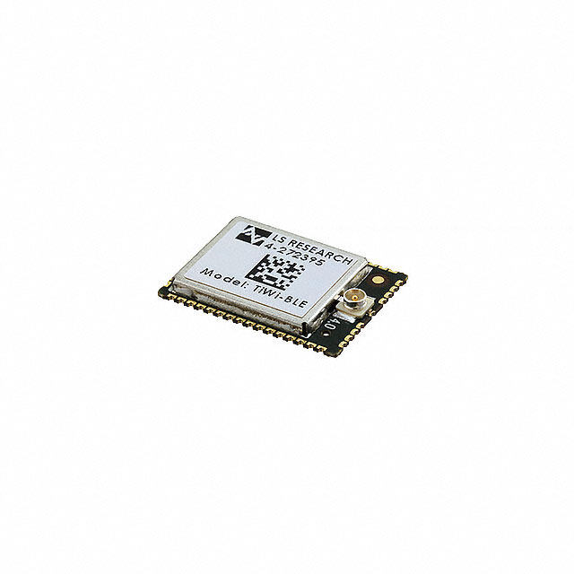
ICGOO在线商城 > 射频/IF 和 RFID > RF 收发器模块 > WYSBMVGX4
- 型号: WYSBMVGX4
- 制造商: TAIYO YUDEN-XENTEK
- 库位|库存: xxxx|xxxx
- 要求:
| 数量阶梯 | 香港交货 | 国内含税 |
| +xxxx | $xxxx | ¥xxxx |
查看当月历史价格
查看今年历史价格
WYSBMVGX4产品简介:
ICGOO电子元器件商城为您提供WYSBMVGX4由TAIYO YUDEN-XENTEK设计生产,在icgoo商城现货销售,并且可以通过原厂、代理商等渠道进行代购。 WYSBMVGX4价格参考。TAIYO YUDEN-XENTEKWYSBMVGX4封装/规格:RF 收发器模块, 。您可以下载WYSBMVGX4参考资料、Datasheet数据手册功能说明书,资料中有WYSBMVGX4 详细功能的应用电路图电压和使用方法及教程。
| 参数 | 数值 |
| 产品目录 | |
| 描述 | RF MODULE DUAL BAND WLANWiFi/802.11模块 W-LAN MOD DUALBAND W/O X'TAL |
| 产品分类 | RF 收发器射频/无线模块 |
| 品牌 | Taiyo Yuden |
| 产品手册 | |
| 产品图片 |
|
| rohs | |
| 产品系列 | WiFi/802.11模块,Taiyo Yuden WYSBMVGX4- |
| 数据手册 | |
| 产品型号 | WYSBMVGX4 |
| 产品种类 | WiFi/802.11模块 |
| 传输功率—最大值 | 16 dBm |
| 其它名称 | 587-3162-1 |
| 功率-输出 | 16dBm |
| 包装 | 剪切带 (CT) |
| 商标 | Taiyo Yuden |
| 天线连接器 | PCB,表面贴装 |
| 存储容量 | - |
| 安全 | AES, WEP, WPA, WPA2 |
| 封装 | Reel |
| 封装/外壳 | 0503(1308 公制) |
| 尺寸 | 13.1 mm x 6.1 mm x 1.35 mm |
| 工作温度 | -10°C ~ 70°C |
| 工作电源电压 | 1.8 V, 3.3 V |
| 工厂包装数量 | 1500 |
| 应用 | 通用 |
| 接口类型 | SDIO |
| 支持协议 | 802.11 a/b/g/n, Bluetooth |
| 数据接口 | PCB,表面贴装 |
| 数据速率 | 11 Mb/s, 54 Mb/s, 150 Mb/s |
| 数据速率(最大值) | 150Mbps |
| 最大工作温度 | + 70 C |
| 最小工作温度 | - 10 C |
| 标准包装 | 1 |
| 灵敏度 | -87dBm |
| 电压-电源 | 1.8V, 3.3V |
| 电流-传输 | - |
| 电流-接收 | - |
| 调制或协议 | 802.11 a/b/g/n |
| 调制技术 | DSSS, OFDM |
| 频带 | 2.4 GHz, 5 GHz |
| 频率 | 2.4GHz,5GHz |



- 商务部:美国ITC正式对集成电路等产品启动337调查
- 曝三星4nm工艺存在良率问题 高通将骁龙8 Gen1或转产台积电
- 太阳诱电将投资9.5亿元在常州建新厂生产MLCC 预计2023年完工
- 英特尔发布欧洲新工厂建设计划 深化IDM 2.0 战略
- 台积电先进制程称霸业界 有大客户加持明年业绩稳了
- 达到5530亿美元!SIA预计今年全球半导体销售额将创下新高
- 英特尔拟将自动驾驶子公司Mobileye上市 估值或超500亿美元
- 三星加码芯片和SET,合并消费电子和移动部门,撤换高东真等 CEO
- 三星电子宣布重大人事变动 还合并消费电子和移动部门
- 海关总署:前11个月进口集成电路产品价值2.52万亿元 增长14.8%



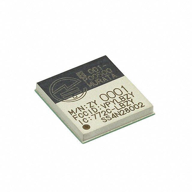
PDF Datasheet 数据手册内容提取
21-May.-2015 Ver1.0 WYSBMVGX4 TAIYO YUDEN Wireless LAN Module IEEE802.11a/b/g/n WYSBMVGX4 Data Report TAIYO YUDEN 1/25
21-May.-2015 Ver1.0 WYSBMVGX4 TAIYO YUDEN Document constituent list Control name Control No. Document Page General Items HD-AG-A091234 1/2 - 2/2 Absolute maximum ratings HD-AM-A091234 1/1 Electrical characteristics HD-AE-A091234 1/9 - 9/9 Circuit schematic HD-MC-A091234 1/1 Outline / Appearance HD-AD-A091234 1/2- 2/2 Pin Layout HD-BA-A091234 1/3 - 3/3 Handling Precaution HQ-BA-523 1/2- 2/2 Taping Specification HD-BB-A091234 1/3 - 3/3 Rev. record 21-May-2015 > Ver1.0 Released TAIYO YUDEN 2/25
21-May.-2015 Ver1.0 WYSBMVGX4 TAIYO YUDEN Control No. Control name HD-AG-A091234 (1/2) General Items Scope This specification (“Specification”) applies to the hybrid IC for use Wireless LAN (“Product”) manufacture by TAIYO YUDEN Co., Ltd. (“TAIYO YUDEN”) 1. Part Number: WYSBMVGX4 2. Function: Radio frequency transfer Module. (IEEE802.11abgn standard conformity) 3. Application: Hand Held Device 4. Structure: Hybrid IC loaded with silicon monolithic and GaAs semiconductor Ability of lead free mounting at customer's assembly (Heat resistance of this Product) : Yes Containment of hazardous substance in this Product *This product conforms to RoHS Directive. 5. Outline: 77-pin leadless chip carrier 6. Marking: Part Number, Lot Number 7. Features: -IEEE802.11abgn standard conformity Interface: SDIO Embedded MPU for reducing loads on host processor Built-in EEPROM (MAC address) 8. Security: WEP (64/128), TKIP, AES, WPA, WPA2, WAPI 9. Packing: Packaging method: Tape and Reel Packaging unit: 1500pcs/reel Package Material: Conductive PS 10. Notes: a. This Product is not designed for radiation durable and should not be used under the circumstance of radiation. b. The operating conditions of this Product are as shown in this Specification. Please note that TAIYO YUDEN shall not be liable for a failure and/or abnormality which is caused by use under the conditions other than the operating conditions hereof. c. This Product mentioned in this Specification is manufactured for use in consumer products. Before using this Product in any special equipment (such as medical equipment, space equipment, air craft, disaster prevention equipment), where higher safety and reliability are duly required, the applicability and suitability of this Product must be fully evaluated by the customer at its sole risk to ensure correct and safety operation of those special equipments. Also, evaluation of the safety function of this Product even for use in general electronics equipment shall be thoroughly made and when necessary, a protective circuit shall be added at design stage, all at the customer’s sole risk. TAIYO YUDEN 3/25
21-May.-2015 Ver1.0 WYSBMVGX4 TAIYO YUDEN Control No. Control name HD-AG-A091234 (2/2) General Items d. i) You are requested to fully check and confirm by the start of mass production of this Product that (1) no bug, defect or other failure is included in firmware incorporated in this Product (“Incorporated Software”), (2) no bug defect or other failure is caused by installation of this Product with Incorporated Software into customer’s products, and that Incorporated Software fully meets customer’s intended use, although TAIYO YUDEN sufficiently inspects or verifies quality of Incorporated Software. ii) Please note that TAIYO YUDEN is not responsible for any failure arising out of bugs or defects in Incorporated Software. e. Communication between this Product and others might not be established nor maintained depending upon radio environment or operating conditions of this Product and other ISM band at 2.4GHz and 5GHz products. f. This Product operates in the unlicensed ISM band at 2.4GHz and 5GHz. In case this Product is used around the other wireless devices which operate in same frequency band of this Product, there is a possibility that interference occurs between this Product and such other devices. If such interference occurs, please stop the operation of other devices or relocate this Product before using this Product or do not use this Product around the other wireless devices. g. Please evaluate adequately our module incorporated to your products before mass production. h. Caution for Export Control This Product may be subject to governmental approvals, consents, licenses, authorizations, declarations, filings, and registrations for export or re-export of the Product, required by Japanese Foreign Exchange and Foreign Trade Law(including related laws and regulations) and/or any other country’s applicable laws or regulations related to export control. In case you will export or re-export this Product, you are strongly recommended to check and confirm, before exporting or re-exporting, necessary procedures for export or re-export of this Product which is required by applicable laws and regulations, and if necessary, you have to obtain necessary and appropriate approvals or licenses from governmental authority at your own risk and expense. TAIYO YUDEN 4/25
21-May.-2015 Ver1.0 WYSBMVGX4 TAIYO YUDEN Control No. Control name HD-AM-A091234 (1/1) Absolute maximum ratings Absolute maximum ratings Rating Item Symbol Remark Min. Typ. Max. Unit Supply voltage 1 VIO - 4.0 V Supply voltage 2 VDD18 - 1.98 V Supply voltage 3 VBAT - 5.6 V Degrees Storage temperature range Tstg -30 100 C Degrees Operation temperature range Topr -20 25 70 C Recommended operating range Rating Item Symbol Remark Min. Typ. Max. Unit Supply voltage 1 VIO 1.62/2.97 1.8/3.3 1.98/3.63 V Supply voltage 2 VDD18 1.71 1.8 1.89 V Supply voltage 3 VBAT 3.2 3.3 4.3 V TAIYO YUDEN 5/25
21-May.-2015 Ver1.0 WYSBMVGX4 TAIYO YUDEN Control No. Control name HD-AE-A091234 (1/9) Electrical characteristics DC Specifications The Specification applies for Topr.= 25 degrees C, Supply voltage=Typical voltage No. Parameter Condition Symbol Min. Typ. Max. Unit Remark 1 Peak Current1 VIO Ip1 - 20 mA 2 Peak Current2 VDD18 Ip2 - 250 mA 3 Peak Current3 VBAT Ip3 - 300 mA 4 Power consumption1 Burst Tx (2G-11n/150Mbps) Pc1 219 mW Duty=2.6% 5 Power consumption2 Continuous Rx (2G-11n/150Mbps) Pc2 242 mW 6 Power consumption3 Burst Tx (2G-11n/72.2Mbps) Pc3 228 mW Duty=4.5% 7 Power consumption4 Continuous Rx (2G-11n/72.2Mbps) Pc4 230 mW 8 Power consumption5 Burst Tx (11g/54Mbps) Pc5 320 mW Duty=20% 9 Power consumption6 Continuous Rx (11g/54Mbps) Pc6 229 mW 10 Power consumption7 Burst Tx (11b/11Mbps) Pc7 520 mW Duty=45% 11 Power consumption8 Continuous Rx (11b/11Mbps) Pc8 230 mW 12 Power consumption9 Burst Tx (5G-11n /150Mbps) Pc9 252 mW Duty=2.6% 13 Power consumption10 Continuous Rx (5G-11n /150Mbps) Pc10 281 mW 14 Power consumption11 Burst Tx (5G-11n /72.2Mbps) P11 261 mW Duty=4.5% Continuous Rx (5G-11n 15 Power consumption12 P12 268 mW /72.2Mbps) 16 Power consumption13 Burst Tx (11a /54Mbps) Pc13 328 mW Duty=20% 17 Power consumption14 Continuous Rx (11a /54Mbps) Pc14 268 mW Power Save Pc15 13 mW VIO=3.3V 18 Power consumption15 (DTIM=1,Beacon Interval=100mS) Pc16 11 mW VIO=1.8V Pc17 3.0 mW VIO=3.3V 19 Power consumption16 Deep Sleep Pc18 0.81 mW VIO=1.8V Pc19 0.35 mW VIO=3.3V 20 Power consumption17 Power Down Pc20 0.11 mW VIO=1.8V Digital Pad Ratings No. Parameter Condition Symbol Min. Typ. Max. Unit Remark 1 Input high voltage VIH 0.8*VIO VIO+0.3 V 2 Input low voltage VIL -0.3 0.3*VIO V 3 Output high voltage VOH VIO-0.4 - V 4 Output low voltage VOL - 0.4 V TAIYO YUDEN 6/25
21-May.-2015 Ver1.0 WYSBMVGX4 TAIYO YUDEN Control No. Control name HD-AE-A091234 (2/9) Electrical characteristics AC Specifications Power-on timing / External sleep clock Conditio Parameter Symbol Min Typ Max Unit Remark n Valid Power / Clock to PDn 1 Tpor 100 ms de-asserted 2 Input SLP_CLK frequency Tf 32.768 KHz 3 Input SLP_CLK high voltage V 0.8 1.8 1.98 V IH 4 Input SLP_CLK low voltage V 0.0 0.25 V IL Input SLP_CLK phase noise 5 PN -125 dBc/Hz @100KHz requirement 6 Input SLP_CLK slew rate limit (10-90%) SR 100 ns 7 Input SLP_CLK duty cycle tolerance DC 20 80 % <Power-on sequence> PDn must remain asserted for minimum of Tpor after VBAT, VIO, VDD18, REF_CLK and SLP_CLK are stable. RESETn must be inactive value (asserted high) when PDn is de-asserted. External reset(RESETn), power down(PDn) Conditio Parameter Symbol Min Typ Max Unit Remark n 211111 RESETn pulse width Trpw 1 ms 211112 PDn pulse width Tppw 100 ms RESETn should be asserted while VBAT, VIO, VDD18, REF_CLK and SLP_CLK are stable and PDn is de-asserted (high level). Trpw RESETn PDn should be asserted while VBAT, VIO, VDD18, REF_CLK and SLP_CLK are stable and RESETn is de-asserted (high level). For lowest current consumption, apply all power rails to WYSBMVGX4 during the assertion of PDn pin. TAIYO YUDEN 7/25
21-May.-2015 Ver1.0 WYSBMVGX4 TAIYO YUDEN Control No. Control name HD-AE-A091234 (3/9) Electrical characteristics Input fast clock specifications (Clock frequency : f (MHz)= 26 / 38.4) Remar Parameter Condition Symbol Min Typ Max Unit k Input REF_CLK 1 V VDD18-0.5 VDD18 VDD18+0.2 V IH high voltage CMOS Input REF_CLK Mode 2 V 0 0 0.4 V IL low voltage Single-ended 3 VLS_IH - - 1.8 V high-level voltage Single-ended 4 VLS_IL 0 - - V low-level voltage Low- Low-swing clock VLS_ 5 0.5 - - V Swing amplitude(pk-pk) Amp Mode Low-swing mid-point VLS_ 6 50 - - MV/s slope Slope Duty 7 Duty cycle 45 50 55 % cycle Offset=1KHz PN - - -130 dBc/Hz 1K REF_CLK Offset=10KHz PN - - -150 dBc/Hz 10K 8 Phase Noise Offset=100KHz PN - - -156 dBc/Hz 26MHz 100K Offset>1MHz PN - - -156 dBc/Hz 1M Offset=1KHz PN - - -126 dBc/Hz 1K REF_CLK Offset=10KHz PN - - -146 dBc/Hz 10K 9 Phase Noise Offset=100KHz PN - - -152 dBc/Hz 38.4MHz 100K Offset>1MHz PN - - -152 dBc/Hz 1M 1000/f 1000/f 10 REF_CLK period Tpxo 1000/f ns -20ppm +20ppm TAIYO YUDEN 8/25
21-May.-2015 Ver1.0 WYSBMVGX4 TAIYO YUDEN Control No. Control name HD-AE-A091234 (4/9) Electrical characteristics SDIO Interface Specifications The Specification applies for Topr.= -20 to 70 degrees C , Supply voltage=Typical voltage Parameter Symbol Condition Min Typ Max Unit Remark Normal 0 - 25 1 Input SDIO_CLK Frequency Tf MHz High Speed 0 - 50 Normal 10 - - 2 Input SDIO_CLK High Time Tch ns High Speed 7 - - Normal 10 - - 3 Input SDIO_CLK Low Time Tcl ns High Speed 7 - - Normal 5 - - 4 Input SDIO_CMD, DATA[3:0] Setup time Tsu ns High Speed 6 - - Normal 5 - - 5 Input SDIO_CMD, DATA[3:0] Hold time Thd ns High Speed 2 - - 6 Output SDIO_CMD, DATA[3:0] Delay time Tod - - - 14 ns 7 Output SDIO_CMD, DATA[3:0] Hold time Toh High Speed 2.5 - - ns Normal Mode Tf SD_CLK Tch Tcl HOST > WiFi Tsu Thd SD_CMD SD_DATA[3:0] WiFi > HOST Tod SD_CMD SD_DATA[3:0] High Speed Mode Tf SD_CLK Tch Tcl HOST > WiFi Tsu Thd SD_CMD SD_DATA[3:0] Toh WiFi > HOST Tod SD_CMD SD_DATA[3:0] TAIYO YUDEN 9/25
21-May.-2015 Ver1.0 WYSBMVGX4 TAIYO YUDEN Control No. Control name HD-AE-A091234 (5/9) Electrical characteristics RF Specifications (WLAN 11b/11Mbps, CCK) The Specification applies for Ta=25 degrees C, Supply voltage=Typical voltage No Parameter Condition Symbol Min Typ Max Unit Remark . 1 RF frequency range FREQ 2412 2472 MHz 2 TX Power Po 14 16 18 dBm 1st Side Lobe M1 - -30 dBc 3 Spectrum Mask 2nd Side Lobe M2 - -50 dBc Power up TU - 2 us 4 Power up-down rump Power down TD - 2 us 5 Frequency tolerance Ft -25 25 ppm 6 EVM Peak EVM - 35 % 7 TX Out of band spurious1 30MHz to 1GHz TOS1 - -36 dBm 8 TX Out of band spurious2 1GHz to 12.75GHz TOS2 - -30 dBm 1.8GHz to 1.9GHz 9 TX Out of band spurious3 TOS3 -47 dBm 5.15GHz to 5.3GHz 10 Rx sensitivity FER<8% SEN - -87 -84 dBm 11 Maximum Input Level FER<8% MIL -10 dBm 12 RX Out of band spurious1 30MHz to 1GHz ROS1 - -57 dBm 13 RX Out of band spurious2 1GHz to 12.75GHz ROS2 - -47 dBm RF Specifications (WLAN 11g/54Mbps, OFDM) The Specification applies for Ta=25 degrees C, Supply voltage =Typical voltage No Parameter Condition Symbol Min Typ Max Unit Remark . 1 RF frequency range FREQ 2412 2472 MHz 2 TX Power Po 13 15 17 dBm 1st Side Lobe M1 - -20 dBc 3 Spectrum Mask 2nd Side Lobe M2 - -28 dBc 3rd Side Lobe M3 - -40 dBc 4 Symbol clock tolerance Ft -25 25 ppm 5 Frequency tolerance Ft -25 25 ppm 6 EVM rms EVM - -25 dB 7 TX Out of band spurious1 30MHz to 1GHz TOS1 - -36 dBm 8 TX Out of band spurious2 1GHz to 12.75GHz TOS2 - -30 dBm 1.8GHz to 1.9GHz 9 TX Out of band spurious3 TOS3 -47 dBm 5.15GHz to 5.3GHz 10 Rx sensitivity PER<10% SEN - -74 -71 dBm 11 Maximum Input Level PER<10% MIL -20 - dBm 12 RX Out of band spurious1 30MHz to 1GHz ROS1 - -57 dBm 12 RX Out of band spurious2 1GHz to 12.75GHz ROS2 - -47 dBm TAIYO YUDEN 10/25
21-May.-2015 Ver1.0 WYSBMVGX4 TAIYO YUDEN Control No. Control name HD-AE-A091234 (6/9) Electrical characteristics RF Specifications (WLAN 11n/MCS7, BW=20MHz, OFDM) The Specification applies for Ta=25 degrees C, Supply voltage =Typical voltage No Parameter Condition Symbol Min Typ Max Unit Remark . 1 RF frequency range FREQ 2412 2472 MHz 2 TX Power Po 12 14 16 dBm 1st Side Lobe M1 - -20 dBc 3 Spectrum Mask 2nd Side Lobe M2 - -28 dBc 3rd Side Lobe M3 - -45 dBc 4 Symbol clock tolerance Ft -25 25 ppm 5 Frequency tolerance Ft -25 25 ppm 6 EVM rms EVM - -28 dB 7 TX Out of band spurious1 30MHz to 1GHz TOS1 - -36 dBm 8 TX Out of band spurious2 1GHz to 12.75GHz TOS2 - -30 dBm 1.8GHz to 1.9GHz 9 TX Out of band spurious3 TOS3 -47 dBm 5.15GHz to 5.3GHz 10 Rx sensitivity PER<10% SEN - -71 -68 dBm 11 Maximum Input Level PER<10% MIL -20 - dBm 12 RX Out of band spurious1 30MHz to 1GHz ROS1 - -57 dBm 13 RX Out of band spurious2 1GHz to 12.75GHz ROS2 - -47 dBm RF Specifications (WLAN 11n/MCS7, BW=40MHz, OFDM) The Specification applies for Ta=25 degrees C, Supply voltage =Typical voltage No Parameter Condition Symbol Min Typ Max Unit Remark . 1 RF frequency range FREQ 2422 2462 MHz 2 TX Power Po 12 14 16 dBm 1st Side Lobe M1 - -20 dBc 3 Spectrum Mask 2nd Side Lobe M2 - -28 dBc 3rd Side Lobe M3 - -45 dBc 4 Symbol clock tolerance Ft -25 25 ppm 5 Frequency tolerance Ft -25 25 ppm 6 EVM rms EVM - -28 dB 7 TX Out of band spurious1 30MHz to 1GHz TOS1 - -36 dBm 8 TX Out of band spurious2 1GHz to 12.75GHz TOS2 - -30 dBm 1.8GHz to 1.9GHz 9 TX Out of band spurious3 TOS3 -47 dBm 5.15GHz to 5.3GHz 10 Rx sensitivity PER<10% SEN - -67 -64 dBm 11 Maximum Input Level PER<10% MIL -20 - dBm 12 RX Out of band spurious1 30MHz to 1GHz ROS1 - -57 dBm 13 RX Out of band spurious2 1GHz to 12.75GHz ROS2 - -47 dBm TAIYO YUDEN 11/25
21-May.-2015 Ver1.0 WYSBMVGX4 TAIYO YUDEN Control No. Control name HD-AE-A091234 (7/9) Electrical characteristics RF Specifications (WLAN 11a/54Mbps, OFDM) The Specification applies for Ta=25 degrees C, Supply voltage =Typical voltage No Parameter Condition Symbol Min Typ Max Unit Remark . 1 RF frequency range FREQ 5180 5825 MHz 2 TX Power Po 12 14 16 dBm 1st Side Lobe M1 - -20 dBc 3 Spectrum Mask 2nd Side Lobe M2 - -28 dBc 3rd Side Lobe M3 - -40 dBc 4 Symbol clock tolerance Ft -20 20 ppm 5 Frequency tolerance Ft -20 20 ppm 6 EVM rms EVM - -25 dB 30MHz to 47MHz, 74MHz to 87.5MHz, 7 TX Out of band spurious1 118MHz to 174MHz, 230MHz to TOS1 - -36 dBm 470MHz, 862MHz to 1GHz 47MHz to 74MHz, 87.5MHz to 118MHz, 8 TX Out of band spurious2 174MHz to 230MHz, 470MHz to TOS2 - -54 dBm 862MHz 9 TX Out of band spurious3 1GHz to 26GHz TOS3 -30 dBm 10 Rx sensitivity PER<10% SEN - -75 -72 dBm 11 Maximum Input Level PER<10% MIL -30 - dBm 12 RX Out of band spurious1 30MHz to 1GHz ROS1 - -57 dBm 13 RX Out of band spurious2 1GHz to 26GHz ROS2 - -47 dBm TAIYO YUDEN 12/25
21-May.-2015 Ver1.0 WYSBMVGX4 TAIYO YUDEN Control No. Control name HD-AE-A091234 (8/9) Electrical characteristics RF Specifications (WLAN 11n/MCS7, BW=20MHz, OFDM) The Specification applies for Ta=25 degrees C, Supply voltage =Typical voltage No Parameter Condition Symbol Min Typ Max Unit Remark . 1 RF frequency range FREQ 5180 5825 MHz 2 TX Power Po 11 13 15 dBm 1st Side Lobe M1 - -20 dBc 3 Spectrum Mask 2nd Side Lobe M2 - -28 dBc 3rd Side Lobe M3 - -45 dBc 4 Symbol clock tolerance Ft -20 20 ppm 5 Frequency tolerance Ft -20 20 ppm 6 EVM rms EVM - -28 dB 30MHz to 47MHz, 74MHz to 87.5MHz, 7 TX Out of band spurious1 118MHz to 174MHz, 230MHz to TOS1 - -36 dBm 470MHz, 862MHz to 1GHz 47MHz to 74MHz, 87.5MHz to 118MHz, 8 TX Out of band spurious2 174MHz to 230MHz, 470MHz to TOS2 - -54 dBm 862MHz 9 TX Out of band spurious3 1GHz to 26GHz TOS3 -30 dBm 10 Rx sensitivity PER<10% SEN - -72 -69 dBm 11 Maximum Input Level PER<10% MIL -30 - dBm 12 RX Out of band spurious1 30MHz to 1GHz ROS1 - -57 dBm 13 RX Out of band spurious2 1GHz to 26GHz ROS2 - -47 dBm TAIYO YUDEN 13/25
21-May.-2015 Ver1.0 WYSBMVGX4 TAIYO YUDEN Control No. Control name HD-AE-A091234 (9/9) Electrical characteristics RF Specifications (WLAN 11n/MCS7, BW=40MHz, OFDM) The Specification applies for Ta=25 degrees C, Supply voltage =Typical voltage N Parameter Condition Symbol Min Typ Max Unit Remark o. 1 RF frequency range FREQ 5190 5815 MHz 2 TX Power Po 11 13 15 dBm 1st Side Lobe M1 - -20 dBc 3 Spectrum Mask 2nd Side Lobe M2 - -28 dBc 3rd Side Lobe M3 - -45 dBc 4 Symbol clock tolerance Ft -20 20 ppm 5 Frequency tolerance Ft -20 20 ppm 6 EVM rms EVM - -28 dB 30MHz to 47MHz, 74MHz to 87.5MHz, 7 TX Out of band spurious1 118MHz to 174MHz, 230MHz to TOS1 - -36 dBm 470MHz, 862MHz to 1GHz 47MHz to 74MHz, 87.5MHz to 118MHz, 8 TX Out of band spurious2 174MHz to 230MHz, 470MHz to TOS2 - -54 dBm 862MHz 9 TX Out of band spurious3 1GHz to 26GHz TOS3 -30 dBm 10 Rx sensitivity PER<10% SEN - -70 -67 dBm 11 Maximum Input Level PER<10% MIL -30 - dBm 12 RX Out of band spurious1 30MHz to 1GHz ROS1 - -57 dBm 13 RX Out of band spurious2 1GHz to 26GHz ROS2 - -47 dBm TAIYO YUDEN 14/25
21-May.-2015 Ver1.0 WYSBMVGX4 TAIYO YUDEN Control No. Control name HD-MC-A091234 (1/1) Circuit Schematic Block Diagram TAIYO YUDEN 15/25
21-May.-2015 Ver1.0 WYSBMVGX4 TAIYO YUDEN Control No. Control name HD-AD-A091234 (1/2) Outline/Appearance OUTLINE Unit: mm 13.1+/-0.2 WYSBMVGX4 2 . 0 - / + 1 Lot No. . 6 1.35Max A B C D E F G H J K L M N 1 2 3 4 5 6 Bottom View Note: Please check the next page for detailed pad sizes on module. TAIYO YUDEN 16/25
21-May.-2015 Ver1.0 WYSBMVGX4 TAIYO YUDEN Control No. Control name HD-AD-A091234 (2/2) Outline/Appearance Module Pad Dimension Unit: mm 5 x 0 . 1 5 0 . 0 Magnified view 5 0 . 0 Recommended Land Pattern Dimension We recommend that pad sizes on mother board and pad sizes on module should be the same. Recommended Metal Mask (Solder Mask) Conditions Thickness of the Metal Mask should be in the range 0.1 mm TAIYO YUDEN 17/25
21-May.-2015 Ver1.0 WYSBMVGX4 TAIYO YUDEN Control No. Control name HD-BA-A091234 (1/3) Pin Layout Pin Descriptions Loc. Pin Name I/O Pwr Domain Description Function A1 GND - - ground PWR A2 GND - - ground PWR A3 ANT I/O - 2G/5G RF (WiFi-11abgn) Antenna RF A4 GND - - ground PWR A5 GND - - ground PWR A6 GND - - ground PWR B1 TDO O VIO JTAG Test Data Output JTAG B3 GND - - ground PWR B4 GND - - ground PWR B5 GND - - ground PWR B6 GND - - ground PWR C1 TDI I VIO JTAG Test Data Input JTAG C2 TCK I VIO JTAG Test Clock Input JTAG C3 RES - - (Reserved) Should be left open - C4 RES - - (Reserved) Should be left open - C5 VBAT I VBAT Battery power supply PWR C6 VBAT I VBAT Battery power supply PWR D1 RESETn I VIO Reset (0: Reset, 1: Normal Operation) CTRL D2 TMS I VIO JTAG Controller Select JTAG D3 RES - - (Reserved) Should be left open - D4 RES - - (Reserved) Should be left open - D5 RES - - (Reserved) Should be left open - D6 RES - - (Reserved) Should be left open - Power Down (no internal pull-up on this pin) E1 PDn I VIO CTRL (0: Full Power Down, 1: Normal Operation) E2 RES - - (Reserved) Should be left open - E3 GND - - Ground PWR E4 GND - - Ground PWR E5 RES - - (Reserved) Should be left open - E6 RES - - (Reserved) Should be left open - F1 VDD18 I VDD18 1.8V power supply PWR F2 VDD18 I VDD18 1.8V power supply PWR F3 GND - - Ground PWR F4 GND - - Ground PWR F5 RES - - (Reserved) Should be left open - F6 VDD18 I VDD18 1.8V power supply PWR TAIYO YUDEN 18/25
21-May.-2015 Ver1.0 WYSBMVGX4 TAIYO YUDEN Control No. Control name HD-BA-A091234 (2/3) Pin Layout Loc. Pin Name I/O Pwr Domain Description Function G1 GND - - Ground PWR G2 RES - - (Reserved) Should be left open - G3 GND - - Ground PWR G4 GND - - Ground PWR G5 GPIO0 I/O VIO GPIO0 CTRL G6 GND - - Ground PWR H1 RES - - (Reserved) Should be left open - H2 GPIO4 I/O VIO GPIO4 CTRL H3 GND - - Ground PWR H4 RES - - (Reserved) Should be left open - H5 GND - - Ground PWR H6 REF_CLK I VDD18 Crystal/Oscillator Input (26/38.4MHz) CLOCK J1 RES - - (Reserved) Should be left open - J2 RES - - (Reserved) Should be left open - J3 GND - - Ground PWR J4 RES - - (Reserved) Should be left open - J5 GND - - Ground PWR J6 RES - - (Reserved) Should be left open - K1 RES - - (Reserved) Should be left open - K2 RES - - (Reserved) Should be left open - K3 RES - - (Reserved) Should be left open - K4 RES - - (Reserved) Should be left open - K5 VBAT I VBAT Battery power supply PWR K6 GND - - Ground PWR L1 GND - - Ground PWR L2 RES - - (Reserved) Should be left open - L3 RES - - (Reserved) Should be left open - L4 RES - - (Reserved) Should be left open - L5 LDO30_OUT O LDO30 3.0V Voltage Output PWR L6 VDD30 I VDD30 3.0/3.3V Digital IO Power Supply PWR M1 SLP_CLK I VDD18 Sleep Clock Input CLOCK M2 RES - - (Reserved) Should be left open - M3 SD_CMD I/O VIO SDIO Command SDIO M4 SD_DATA[0] I/O VIO SDIO Data[0] SDIO M5 WL_HOST_WKUP O VIO WLAN -> Host Wake up (GPIO16) CTRL M6 VIO I VIO 1.8V/3.3V Digital IO Power Supply PWR TAIYO YUDEN 19/25
21-May.-2015 Ver1.0 WYSBMVGX4 TAIYO YUDEN Control No. Control name HD-BA-A091234 (3/3) Pin Layout Loc. Pin Name I/O Pwr Domain Description Function N1 GND - - Ground PWR N2 SD_DATA[2] I/O VIO SDIO Data[2] SDIO N3 SD_DATA[3] I/O VIO SDIO Data[3] SDIO N4 SD_CLK I VIO SDIO Clock SDIO N5 SD_DATA[1] I/O VIO SDIO Data[1] SDIO N6 GND - - Ground PWR TAIYO YUDEN 20/25
21-May.-2015 Ver1.0 WYSBMVGX4 TAIYO YUDEN Control No. Control name HQ-BA-523 (1/2) Handling Precaution This specification describes desire and conditions especially for mounting. Desire/Conditions (1) Environment conditions for use and storage 1. Store the components in an environment of < 40deg-C/90%%%%RH if they are in a moisture barrier bag packed by TAIYO YUDEN. 2. Keep the factory ambient conditions at < 30deg-C/60%%%%RH . 3. Store the components in an environment of < 25±5deg-C/10%RH after the bag is opened. (The condition is also applied to a stay in the manufacture process). (2) Conditions for handling of products Make sure all of the moisture barrier bags have no holes, cracks or damages at receiving. If an abnormality is found on the bag, its moisture level must be checked in accordance with 2 in (2). Refer to the label on the bag. 1.All of the surface mounting process (reflow process) must be completed in 12 months from the bag sea date. 2. Make sure humidity in the bag is less than 10%RH immediately after open, using a humidity indicator card sealed with the components. 3. All of the surface mounting process (reflow process including rework process) must be completed in 168 hours after the bag is opened (inclusive of any other processes). 4. If any conditions in (1) or condition 2 and 3 in (2) are not met, bake the components in accordance with the conditions at 125deg-C 24hours 5. As a rule, baking the components in accordance with conditions 4 in (2) shall be once. 6. Since semi-conductors are inside of the components, they must be free from static electricity while handled.(<100V) Use ESD protective floor mats, wrist straps, ESD protective footwear, air ionizers etc. , if necessary. 7. Please make sure that there are lessen mechanical vibration and shock for this mo dule, and do not drop it. TAIYO YUDEN 21/25
21-May.-2015 Ver1.0 WYSBMVGX4 TAIYO YUDEN Control No. Control name HQ-BA-523 (2/2) Handling Precaution 8. Please recognize pads of back side at surface mount. 9. Please do not wash this module. 10. Please perform temperature conditions of module at reflow within the limits of the following. Please give the number of times of reflow as a maximum of 2 times. Recommented Reflow Profile 300 Temp(deg) Peak Temp:250deg Max 250 230deg up : 40secMax 200 150 100 130-180deg Pre-heat : 60~120sec 50 0 IN OUT TAIYO YUDEN 22/25
21-May.-2015 Ver1.0 WYSBMVGX4 TAIYO YUDEN Control No. Control name HD-BB-A091234 (1/3) Taping Specification Packaging Specification (1) Packaging Material Name Outline Materials Note Emboss 24mm wide-12mmPitch Conductive PS Cover Tape Reel φ330mm Conductive PS Desiccant 30g x 1 Humidity indicator card Aluminum moisture barrier bag 420 x 460(mm) (AS)Polyester/AL/Nylon /Polyethylene(AS) Label Corrugated cardboard 376x 376 x52(mm) Box(Inner) Corrugated cardboard 400 x 390 x290(mm) Box(Outer) (2) Packaging Unit Max 1500 pieces/Reel Max 7500 pieces/Box (Outer) (3)Packaging Figure Humidity indicator card Desiccant Aluminum Corrugated <CPu/sNt>omerC uNsatmoemer Part Name Lot No moisture <<TTSA//IYDNO>> YPU/DOTSENeariiPyaalo rNc YuhmausMdbeeAeorrDndE e PIrN a NOrotr igNina omf Ceountry<QTY>Quantity cardboard barrier bag box (inner) Corrugated cardboard Caution Label box(Inner) <<<TCPTSuA/I//sYNDNtO>>>o YPmU/eDOrSCTE NeaurNiPisyaatalom orN cemYuhmaeuMsdbree AeoPrDnrdEa e rPIrNt a NONrotrai gmNin aeomf Ceountry<QTY>Lot QNuoantity (4)The entry item to a Label C<<<TPTSAu///IsYNDNtO>>> oYPmU/eODrCTSE NeaurNiPisyaatalo morN cemYuhmauesMbrdee AeoPrDnrEad e rPINrt aN ONrotrai gmNin aeomf Ceountry<QTY>Lot QNouantity C<Pu/sNt>omerC uNsatmoemer Part Name Lot No <<TTSA//IYDNO>> YPU/ODTSEeNariiPyaalo rN cYuhmausMbdeeAeorDnrEd e PINr aN Orotri gNin aomf Ceountry<QTY>Quantity C<Pu/sNt>omerC uNsatmoemer Part Name Lot No COMPANY NAME <<TTSA//IYDNO>> YPU/ODTSEeNariiPayalo rN cYuhmausMbdeeAeorDnrEd e PINr aN Orotri gNin aomf Ceountry<QTY>Quantity C<<<TPTSAu///IsYNDNtO>>> oYPmU/eODrCTSE NeaurNiPisyaatalo morN cemYuhmauesMbrdee AeoPrDnrEad e rPINrt aN ONrotrai gmNin aeomf Ceountry<QTY>Lot QNouantity PURCHASE ORDER DESCRIPTION CorrugaC<<<TPTSAu///IsYNDNtO>>> oYPmUt/eODrCTES NeaurNiPisyaatalo emorN cemYuhmauesMbrdee AeoPrDnrEad e rPINrt aN ONrotdrai gmNin aeomf Ceountry< QTY>Lot QNouantitycardboard QUANTITY box(Outer) NOTE TAIYO YUDEN 23/25
21-May.-2015 Ver1.0 WYSBMVGX4 TAIYO YUDEN Control No. Control name HD-BB-A091234 (2/3) Taping Specification (5)Tape specification The direction of a tape drawer W Y Lot No. SBMVGX Direction Mark B End part Module receipt part Leader part More than160mm More than 100mm More than 300mm The direction of a tape drawer TAIYO YUDEN 24/25
21-May.-2015 Ver1.0 WYSBMVGX4 TAIYO YUDEN Control No. Control name HD-BB-A091234 (3/3) Taping Specification (6)Reel specification Unit:mm φ330±2 φ13±0.2 W-1.5/+2 Tape wide 8mm 12mm 16mm 24mm 32mm 44mm W 9.4mm 13.4mm 17.4mm 25.4mm 33.4mm 45.4mm (7) Taping performance Both of an embossing tape top cover tape bear this, when the power of 10N is applied in the direction of a drawer. The exfoliation adhesion of a top cover tape is the intensity of 0.1~1.3N. (The angle to pull is 165~180 deg-C. The speed to pull is 300 mm/min.) (8)Note Lack of the parts in 1 reel is with two or less pieces. TAIYO YUDEN 25/25
Mouser Electronics Authorized Distributor Click to View Pricing, Inventory, Delivery & Lifecycle Information: T aiyo Yuden: WYSBMVGX4
 Datasheet下载

