ICGOO在线商城 > WR04X1001FTL
 Datasheet下载
- 型号: WR04X1001FTL
- 制造商: Walsin
- 库位|库存: xxxx|xxxx
- 要求:
| 数量阶梯 | 香港交货 | 国内含税 |
| +xxxx | $xxxx | ¥xxxx |
查看当月历史价格
查看今年历史价格
WR04X1001FTL产品简介:
ICGOO电子元器件商城为您提供WR04X1001FTL由Walsin设计生产,在icgoo商城现货销售,并且可以通过原厂、代理商等渠道进行代购。 提供WR04X1001FTL价格参考¥0.00-¥0.00以及WalsinWR04X1001FTL封装/规格参数等产品信息。 你可以下载WR04X1001FTL参考资料、Datasheet数据手册功能说明书, 资料中有WR04X1001FTL详细功能的应用电路图电压和使用方法及教程。
| 参数 | 数值 |
| 品牌 | Walsin |
| 产品目录 | 无源元件 |
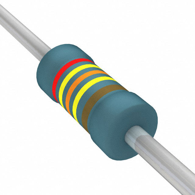
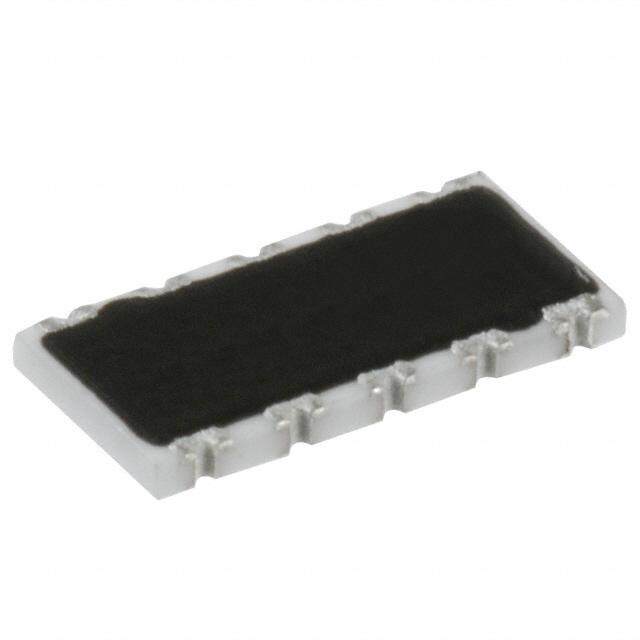
| 描述 | 厚膜电阻器 - SMD 1K ohms 1% 0402 |
| 产品分类 | |
| 产品手册 | |
| 产品图片 |
|
| rohs | 符合RoHS |
| 产品系列 | 薄膜电阻器,厚膜电阻器 - SMD,Walsin WR04X1001FTL |
| 产品型号 | WR04X1001FTL |
| 产品 | Thick Film Resistors SMD |
| 产品种类 | 厚膜电阻器 - SMD |
| 功率额定值 | 62.5 mW (1/16 W) |
| 商标 | Walsin |
| 外壳代码-in | 0402 |
| 外壳代码-mm | 1005 |
| 外壳宽度 | 0.5 mm |
| 外壳长度 | 1 mm |
| 外壳高度 | 0.35 mm |
| 容差 | 1 % |
| 封装 | Reel |
| 封装/箱体 | 0402 (1005 metric) |
| 工作温度范围 | - 55 C to + 155 C |
| 工厂包装数量 | 10000 |
| 温度系数 | 100 PPM / C |
| 电压额定值 | 50 V |
| 电阻 | 1 kOhms |
| 类型 | General Purpose Chip Resistors |
| 系列 | WR04X |


- 商务部:美国ITC正式对集成电路等产品启动337调查
- 曝三星4nm工艺存在良率问题 高通将骁龙8 Gen1或转产台积电
- 太阳诱电将投资9.5亿元在常州建新厂生产MLCC 预计2023年完工
- 英特尔发布欧洲新工厂建设计划 深化IDM 2.0 战略
- 台积电先进制程称霸业界 有大客户加持明年业绩稳了
- 达到5530亿美元!SIA预计今年全球半导体销售额将创下新高
- 英特尔拟将自动驾驶子公司Mobileye上市 估值或超500亿美元
- 三星加码芯片和SET,合并消费电子和移动部门,撤换高东真等 CEO
- 三星电子宣布重大人事变动 还合并消费电子和移动部门
- 海关总署:前11个月进口集成电路产品价值2.52万亿元 增长14.8%


PDF Datasheet 数据手册内容提取
Approval sheet WR12, WR08, WR06, WR04 1%, 5% Thick Film General Purpose Chip Resistors Size 1206, 0805, 0603, 0402 RoHS 2 compliant & Halogen free *Contents in this sheet are subject to change without prior notice. Page 1 of 10 ASC_WR_V24 SEP 2016
Approval sheet FEATURE 1. High reliability and stability 2. Reduced size of final equipment 3. Lower assembly costs 4. Higher component and equipment reliability 5. RoHS 2 compliant and Halogen free products APPLICATION Consumer electrical equipment EDP, Computer application Telecom application DESCRIPTION The resistors are constructed in a high grade ceramic body (aluminum oxide). Internal metal electrodes are added at each end and connected by a resistive paste that is applied to the top surface of the substrate. The composition of the paste is adjusted to give the approximate resistance required and the value is trimmed to within tolerance by laser cutting of this resistive layer. The resistive layer is covered with a protective coat. Finally, the two external end terminations are added. For ease of soldering the outer layer of these end terminations is a Tin (lead free) alloy. Fig 1. Construction of Chip-R Page 2 of 10 ASC_WR_V24 SEP 2016
Approval sheet QUICK REFERENCE DATA Item General Specification Series No. WR12 WR08 WR06 WR04 Size code 1206(3216) 0805(2012) 0603(1608) 0402(1005) Resistance Range 1~10M (5% tolerance), Jumper 1~10M (1% tolerance), Resistance Tolerance 1% 5% 1% 5% 1% 5% 1% 5% E96/E24 E24 E96/E24 E24 E96/E24 E24 E96/E24 E24 TCR (ppm/C) 10M R>10 100 R10 -200~+400 Max. dissipation 1/4 W 1/8 W 1/10 W 1/16 W @ T =70C amb Max. Operation 200V 150V 75V 50V Voltage (DC or RMS) Max. Overload 400V 300V 150V 100V Voltage (DC or RMS) Climatic category 55/155/56 Note : 1. This is the maximum voltage that may be continuously supplied to the resistor element, see “IEC publication 60115-8” 2. Max. Operation Voltage : So called RCWV (Rated Continuous Working Voltage) is determined by RCWV Rated PowerResistance Valueor Max. RCWV listed above, whichever is lower. 3. The resistance of Jumper is defined <0.05. DIMENSIONS (unit : mm) WR12 WR08 WR06 WR04 L 3.10 0.10 2.00 0.10 1.60 0.10 1.00 0.05 W 1.60 0.10 1.25 0.10 0.80 0.10 0.50 0.05 T 0.60 0.15 0.50 0.15 0.45 0.15 0.35 0.05 Tb 0.45 0.20 0.40 0.20 0.30 0.15 0.25 0.10 Tt 0.50 0.20 0.40 0.20 0.30 0.10 0.20 0.10 Page 3 of 10 ASC_WR_V24 SEP 2016
Approval sheet MARKING Size \ Nr. Of digit of code\tolerance 5% 1% 1206 (3216) 3-digits marking 4-digits marking 0805 (2012) 3-digits marking 4-digits marking 0603 (1608) 3-digits marking 3-digits marking 0402(1005) N0 MARKING 3-digits marking(5% : 1206 & 0805 & 0603 ) Each resistor is marked with a three digits code on the protective coating to designate the nominal resistance value. 3-digits marking(1% : 0603) Nominal resistance Description 1.E-24 series As 0603 WR06X 5%. 2.E-96 series The 1st two digit codes are referring to the CODE on the table, the 3rd code is the index of resistance value : Y=10-2,X=10-1,A=100,B=101,C=102,D=103,E=104,F=105 EX : 17.8Ω=25X,178Ω=25A,1K78 =25B 17K8=25C, 178K=25D, 1M78=25E 3. Remark There is no marking for the items are not under E-24 and E-96 series CODE R_value CODE R_value CODE R_Value CODE R_value CODE R_value CODE R_value CODE R_value CODE R_value 01 100 13 133 25 178 37 237 49 316 61 422 73 562 85 750 02 102 14 137 26 182 38 243 50 324 62 432 74 576 86 768 03 105 15 140 27 187 39 249 51 332 63 442 75 590 87 787 04 107 16 143 28 191 40 255 52 340 64 453 76 604 88 806 05 110 17 147 29 196 41 261 53 348 65 464 77 619 89 825 06 113 18 150 30 200 42 267 54 357 66 475 78 634 90 845 07 115 19 154 31 205 43 274 55 365 67 487 79 649 91 866 08 118 20 158 32 210 44 280 56 374 68 499 80 665 92 887 09 121 21 162 33 215 45 287 57 383 69 511 81 681 93 909 10 124 22 165 34 221 46 294 58 392 70 523 82 698 94 931 11 127 23 169 35 226 47 301 59 402 71 536 83 715 95 953 12 130 24 174 36 232 48 309 60 412 72 549 84 732 96 976 4-digits marking(1% : 1206/0805) Each resistor is marked with a four digits code on the protective coating to designate the nominal resistance value. Example RESISTANCE 10 12 100 6800 47000 3-digits marking(1206 & 0805 & 0603 5% ) 100 120 101 682 473 4-digits marking 10R0 12R0 1000 6801 4702 Page 4 of 10 ASC_WR_V24 SEP 2016
Approval sheet FUNCTIONAL DESCRIPTION Product characterization Standard values of nominal resistance are taken from the E24 series for resistors with a tolerance of 5%, and E96 series for resistors with a tolerance of 1%. The values of the E24/E96 series are in accordance with “IEC publication 60063” Derating The power that the resistor can dissipate depends on the operating temperature; see Fig.2 Figure 2 Maximum dissipation in percentage of rated power as a function of the ambient temperature for WR12, WR08, WR06, WR04 MOUNTING Due to their rectangular shapes and small tolerances, Surface Mountable Resistors are suitable for handling by automatic placement systems. Chip placement can be on ceramic substrates and printed-circuit boards (PCBs). Electrical connection to the circuit is by individual soldering condition. Storage and Handling Conditions: 1. Products are recommended to be used up within two years since operation date as ensured shelf life. Check solderability in case shelf life extension is needed. 2. To store products with following condition: Temperature :5 to 40℃ Humidity :20 to 70% relative humidity 3. Caution: a.Don't store products in a corrosive environment such as sulfide, chloride gas, or acid. It may cause oxdization of electrode, which easily be resulted in poor soldering b.To store products on the shelf and avoid exposure to moisture. c.Don't expose products to excessive shock, vibration, direct sunlight and so on Page 5 of 10 ASC_WR_V24 SEP 2016
Approval sheet SOLDERING CONDITION follows J-STD-020D The robust construction of chip resistors allows them to be completely immersed in a solder bath of 260C for 10 seconds. Therefore, it is possible to mount Surface Mount Resistors on one side of a PCB and other discrete components on the reverse (mixed PCBs). Surface Mount Resistors are tested for solderability at 235C during 2 seconds. The test condition for no leaching is 260C for 30 seconds. Typical examples of soldering processes that provide reliable joints without any damage are given in Fig 3. Fig 3. Infrared soldering profile for Chip Resistors CATALOGUE NUMBERS The resistors have a catalogue number starting with WR12 X 472_ J T L Size code Type code Resistance code Tolerance Packaging code Termination code WR12 : 1206 X : 5%, E24: 2 significant F : 1% T : 7” Reeled taping L= Sn base digits followed by no. of (lead free) WR08 : 0805 Jumper zeros and a blank J : 5% Q : 10” Reeled taping WR06 : 0603 5%, 1 ~ 10M P : Jumper G : 13” Reeled taping 4.7 =4R7_ WR04: 0402 1%, 10 ~ 1M H : 13'' reel 50Kpcs 10 =100_ only for 0402 W : 220 =221_ B : Bulk 1%, < 10; >1M Jumper =000_ D : 7'' reel 20Kpcs (“_” means a blank) only for 0402 1%, E24+E96: 3 significant A : 7" reel 15Kpcs only digits followed by no. of for 0402 zeros 102 =1020 37.4K =3742 WR12, WR08, WR06: 1. Reeled tape packaging : 8mm width paper taping 5000pcs per 7” reel, 10kpcs per 10” reel, 20kpcs per 13” reel. 2. Bulk packaging : 5000pcs per poly-bag Page 6 of 10 ASC_WR_V24 SEP 2016
Approval sheet WR04: 1. Reeled tape packaging : 8mm width paper taping 10,000pcs per 7” reel, 20,000pcs per 10” reel. 70,000pcs per 13” reel. 2. Bulk packaging : 10,000pcs per poly-bag Page 7 of 10 ASC_WR_V24 SEP 2016
Approval sheet TEST AND REQUIREMENTS Essentially all tests are carried out according to the schedule of IEC publication 115-8, category LCT/UCT/56(rated temperature range : Lower Category Temperature, Upper Category Temperature; damp heat, long term, 56 days). The testing also meets the requirements specified by EIA, EIAJ and JIS. The tests are carried out in accordance with IEC publication 68, "Recommended basic climatic and mechanical robustness testing procedure for electronic components" and under standard atmospheric conditions according to IEC 60068-1, subclause 5.3. Unless otherwise specified, the following value supplied : Temperature: 15°C to 35°C. Relative humidity: 45% to 75%. Air pressure: 86kPa to 106 kPa (860 mbar to 1060 mbar). All soldering tests are performed with midly activated flux. REQUIREMENT TEST PROCEDURE / TEST METHOD Resistor 0 Electrical - DC resistance values measurement Within the specified tolerance Characteristics - Temperature Coefficient of Resistance (T.C.R) Refer to “QUICK REFERENCE Natural resistance change per change in degree centigrade. DATA” JISC5201-1: 1998 R R <50m 2 1 106 (ppm/C) t : 20°C+5°C-1°C; t : -55°C or +155°C Clause 4.8 1 2 R t t 1 2 1 R : Resistance at reference temperature (20°C+5°C/-1°C) 1 R : Resistance at test temperature (-55°C or +155°C) 2 Resistance to Un-mounted chips completely immersed for 10±1second in a SAC 5%:R/Rmax.(1%+0.05) soldering heat(R.S.H) solder bath at 260℃±5ºC 1%:R/Rmax.(0.5%+0.05) <50m JISC5201-1:1998 no visible damage Clause 4.18 Un-mounted chips completely immersed for 2±0.5 second in a SAC Solderability 95% coverage min., good tinning and no solder bath at 235℃±5℃ JISC5201-1: 1998 visible damage Clause 4.17 Temperature cycling 30 minutes at -55C3C, 2~3 minutes at 20°C+5°C-1°C, 30 minutes at 5%: R/R max. (1%+0.05) +155C3C, 2~3 minutes at 20°C+5°C-1°C, total 5 continuous cycles JISC5201-1: 1998 1%:R/Rmax.(0.5%+0.05) <50m Clause 4.19 No visible damage High Temperature 1000+48/-0 hours; without load in a temperature chamber 5%:R/Rmax.(2%+0.1) Exposure controlled 1553C 1%:R/Rmax.(1%+0.1) <50m MIL-STD-202 No visible damage method 108 Bending strength Resistors mounted on a 90mm glass epoxy resin PCB(FR4), bending 5%:R/Rmax.(1%+0.05) JISC5201-1: 1998 once 3mm for 10sec, 5mm for WR04 1%:R/Rmax.(1%+0.05) <50m Clause 4.33 No visual damaged Adhesion Pressurizing force: 5N, Test time: 10±1sec. No remarkable damage or removal of the JISC5201-1: 1998 terminations Clause 4.32 Short Time Overload 2.5 times RCWV or max. overload voltage, for 5seconds 5%: R/R max. (2%+0.05) (STOL) 1%: R/R max. (1%+0.05) <50m JISC5201-1: 1998 No visible damage Clause 4.13 Page 8 of 10 ASC_WR_V24 SEP 2016
Approval sheet REQUIREMENT TEST PROCEDURE / TEST METHOD Resistor 0 Load life in Humidity 1000 +48/-0 hours, loaded with RCWV or Vmax in humidity chamber 5%: R/R max. (2%+0.1) controller at 40C2C and 90~95% relative humidity, 1.5hours on and JISC5201-1: 1998 1%: R/R max. (1%+0.1) <50m 0.5 hours off Clause 4.24 No visible damage Load life (endurance) 1000 +48/-0 hours, loaded with RCWV or Vmax in chamber controller 5%: R/R max. (3%+0.1) 70±2ºC, 1.5 hours on and 0.5 hours off JISC5201-1: 1998 1%: R/R max. (1%+0.1) <50m Clause 4.25 No visible damage Insulation Resistance Apply the maximum overload voltage (DC) for 1minute R≧10GΩ JISC5201-1: 1998 Clause 4.6 Dielectric Withstand Apply the maximum overload voltage (AC) for 1 minute No breakdown or flashover Voltage JISC5201-1: 1998 Clause 4.7 TEST CONDITION FOR JUMPER (0 ) Item WR12 WR08 WR06 WR04 Power Rating At 70C 1/4W 1/8W 1/10W 1/16W Resistance MAX.50m Rated Current 2A 1.5A 1A 1A Peak Current 5A 3.5A 3A 2A Operating Temperature -55 ~ +155C Page 9 of 10 ASC_WR_V24 SEP 2016
Approval sheet PACKAGING Paper Tape specifications (unit :mm) Series No. A B W F E WR12 3.60±0.20 2.00±0.20 WR08 2.40±0.20 1.65±0.20 8.00±0.30 3.50±0.20 1.75±0.10 WR06 1.90±0.20 1.10±0.20 WR04 1.20±0.10 0.70±0.10 Series No. P1 P0 D T WR12 / WR08 Max. 1.0 4.00±0.10 WR06 4.00±0.10 1.500.1 0.65±0.05 0.0 WR04 2.00±0.10 0.40±0.05 7” Reel dimensions Symbol A B C D 7” reel 178.0±2.0 60.0±1.0 13.0±0.2 9.0±0.5 10” reel 254.0±2.0 100.0±1.0 13.0±0.2 9.0±0.5 13” reel 330.0±2.0 100.0±1.0 13.0±0.2 9.0±0.5 Page 10 of 10 ASC_WR_V24 SEP 2016
Mouser Electronics Authorized Distributor Click to View Pricing, Inventory, Delivery & Lifecycle Information: W alsin: WR04X1001FTL WR04X1002FTL WR04X1003FTL WR04X1004FTL WR04X10R0FTL WR04X1301FTL WR04X4700FTL WR04X4701FTL WR06X1001FTL WR06X1002FTL WR06X1003FTL WR06X4702FTL WR08X1003FTL WR06X1581FTL WR04X8022FTL WR06X6191FTL WR12X000 PTL WR12W1R00FTL WR04X000PTL WR04X1872FTL WR04X7320FTL WR06X3920FTL WR04X823 JTL WR04X2742FTL WR04X6193FTL WR12X3303FTL WR06X33R2FTL WR04X1401FTL WR04X3573FTL WR04X4320FTL WR04X2210FTL WR06X7322FTL WR04X2322FTL WR04X4422FTL WR06X6810FTL WR06X2372FTL WR04X1783FTL WR04X3923FTL WR06X1301FTL WR06X2260FTL WR04X3303FTL WR04X7872FTL WR06X7682FTL WR04X4870FTL WR04X3742FTL WR06X56R2FTL WR04X6340FTL WR04X7501FTR WR06X103 JTR WR04X5112FTR WR12X2203FTL WR04X1R3 JTL WR04X4702FTR WR04X84R5FTL WR06X4120FTL WR04X1503FTR WR04X1202FTR WR04X35R7FTL WR04X4703FTR WR04X1211FTR WR12X5621FTL WR04X1243FTL WR04X3403FTL WR04X18R2FTL WR06X1243FTL WR04X1130FTR WR04X6191FTR WR08X000 PGL WR06X1202FTR WR06X4530FTL WR04X1913FTL WR06X4222FTL WR04X4872FTL WR04X1000FQL WR06X7152FTL WR04X3483FTL WR04X4531FTR WR04X5230FTL WR06X331 JTR WR04X2743FTL WR04X333 JTL