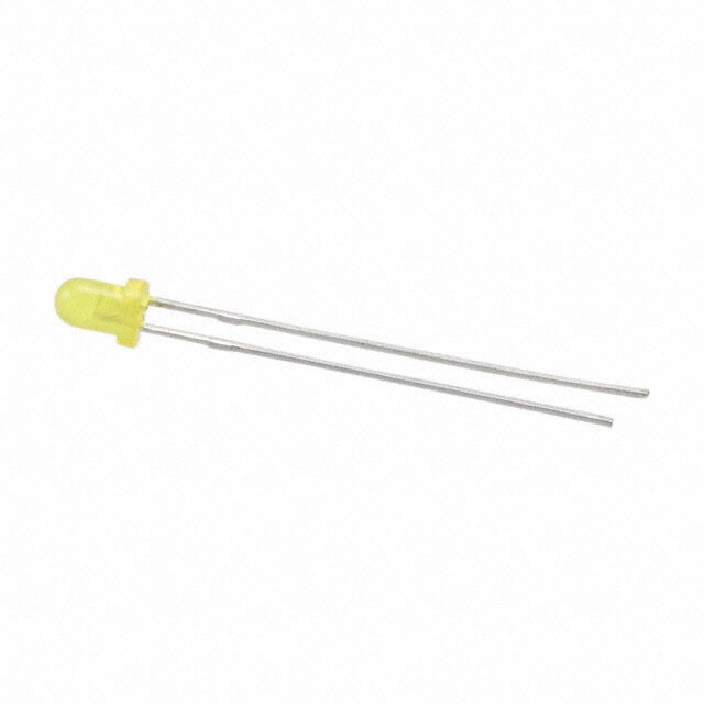
ICGOO在线商城 > 光电元件 > LED 指示 - 分立 > WP115VEGW
- 型号: WP115VEGW
- 制造商: Kingbright
- 库位|库存: xxxx|xxxx
- 要求:
| 数量阶梯 | 香港交货 | 国内含税 |
| +xxxx | $xxxx | ¥xxxx |
查看当月历史价格
查看今年历史价格
WP115VEGW产品简介:
ICGOO电子元器件商城为您提供WP115VEGW由Kingbright设计生产,在icgoo商城现货销售,并且可以通过原厂、代理商等渠道进行代购。 WP115VEGW价格参考¥0.18-¥0.18。KingbrightWP115VEGW封装/规格:LED 指示 - 分立, 绿色,红色 568nm 绿色,617nm 红色 LED 指示 - 分立 2.2V 绿色,2V 红色 径向 - 3 引线。您可以下载WP115VEGW参考资料、Datasheet数据手册功能说明书,资料中有WP115VEGW 详细功能的应用电路图电压和使用方法及教程。
| 参数 | 数值 |
| 产品目录 | |
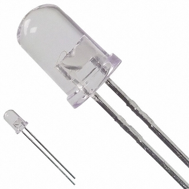
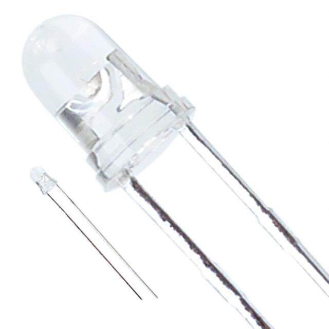
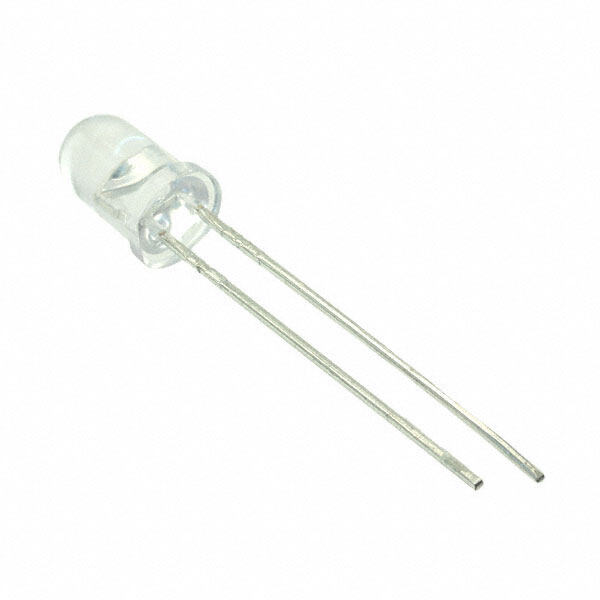
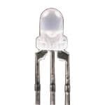
| 描述 | LED 3MM 627/565NM RD/GN WH DIFF标准LED-通孔 Red Green 625 568nm Diffused 50 30mcd |
| 产品分类 | |
| LED大小 | T-1 |
| 品牌 | KingbrightKingbright Company LLC |
| 产品手册 | |
| 产品图片 |
|
| rohs | 符合RoHS无铅 / 符合限制有害物质指令(RoHS)规范要求 |
| 产品系列 | LED发射器,标准LED-通孔,Kingbright WP115VEGW- |
| 数据手册 | |
| 产品型号 | WP115VEGWWP115VEGW |
| 产品种类 | 标准LED-通孔 |
| 光强度 | 50 mcd, 30 mcd |
| 其它名称 | 754-1708 |
| 包装 | 散装 |
| 商标 | Kingbright |
| 大小/尺寸 | - |
| 安装类型 | 通孔 |
| 安装风格 | Through Hole |
| 封装 | Bulk |
| 封装/外壳 | 径向 - 3 引线 |
| 工厂包装数量 | 500 |
| 显示角 | 60 deg |
| 最大工作温度 | + 85 C |
| 最小工作温度 | - 40 C |
| 标准包装 | 500 |
| 正向电流 | 20 mA |
| 毫烛光等级 | 50mcd 绿,50mcd 红 |
| 波长-主 | 568nm,625nm |
| 波长-峰值 | 565nm,627nm |
| 波长/色温 | 625 nm, 568 nm |
| 测试电流时的光通量 | - |
| 照明颜色 | Red, Green |
| 电压-正向(Vf)(典型值) | 2.2V 绿,2V 红 |
| 电流-测试 | 20mA |
| 类型 | Bi-Color Indicator Lamp |
| 视角 | 60° |
| 透镜尺寸 | 3 mm |
| 透镜形状 | Round |
| 透镜样式/尺寸 | 圆形,带圆顶,3mm,T-1 |
| 透镜类型 | 散射,白色 |
| 透镜颜色/类型 | Tinted, Diffused |
| 颜色 | 绿,红 |
| 高度 | 5.00mm |



- 商务部:美国ITC正式对集成电路等产品启动337调查
- 曝三星4nm工艺存在良率问题 高通将骁龙8 Gen1或转产台积电
- 太阳诱电将投资9.5亿元在常州建新厂生产MLCC 预计2023年完工
- 英特尔发布欧洲新工厂建设计划 深化IDM 2.0 战略
- 台积电先进制程称霸业界 有大客户加持明年业绩稳了
- 达到5530亿美元!SIA预计今年全球半导体销售额将创下新高
- 英特尔拟将自动驾驶子公司Mobileye上市 估值或超500亿美元
- 三星加码芯片和SET,合并消费电子和移动部门,撤换高东真等 CEO
- 三星电子宣布重大人事变动 还合并消费电子和移动部门
- 海关总署:前11个月进口集成电路产品价值2.52万亿元 增长14.8%


PDF Datasheet 数据手册内容提取
WP115VEGW T-1 (3mm) Bi-Color Indicator Lamp DESCRIPTIONS PACKAGE DIMENSIONS The High Efficiency Red source color devices are (cid:122) made with Gallium Arsenide Phosphide on Gallium Phosphide Orange Light Emitting Diode The Green source color devices are made with (cid:122) Gallium Phosphide Green Light Emitting Diode FEATURES Uniform light output (cid:122) Low power consumption (cid:122) 3 leads with one common lead (cid:122) Long life-solid state reliability (cid:122) RoHS compliant (cid:122) APPLICATIONS Status indicator (cid:122) Illuminator (cid:122) Signage applications (cid:122) Decorative and entertainment lighting (cid:122) Commercial and residential architectural lighting (cid:122) Notes: 1. All dimensions are in millimeters (inches). 2. Tolerance is ±0.25(0.01") unless otherwise noted. 3. Lead spacing is measured where the leads emerge from the package. 4. The specifications, c haracteristics and technical data described in the datasheet are subject to change without prior notice. SELECTION GUIDE Iv (mcd) @ 20mA [2] V i e w i n g Angle [1] Emitting Color Part Number Lens Type (Material) Min. Typ. 2θ1/2 12 30 ■ High Efficiency Red (GaAsP/GaP) *8 *20 WP115VEGW White Diffused 60° 10 30 ■ Green (GaP) *10 *30 Notes: 1. θ1/2 is the angle from optical centerline where the luminous intensity is 1/2 of the optical peak value. 2. Luminous intensity / luminous flux: +/-15%. * Luminous intensity value is traceable to CIE127-2007 standards. Page 1 / 5 © 2017 Kingbright. All Rights Reserved. Spec No: DSAF1534 / 1101000785 Rev No: V.9A Date: 07/03/2017
WP115VEGW ELECTRICAL / OPTICAL CHARACTERISTICS at T =25°C A Value Parameter Symbol Emitting Color Unit Typ. Max. High Efficiency Red 627 Wavelength at Peak Emission IF = 20mA λpeak Green 565 nm High Efficiency Red 617 Dominant Wavelength IF = 20mA λdom [1] Green 568 nm Spectral Bandwidth at 50% Φ REL MAX High Efficiency Red 45 Δλ nm IF = 20mA Green 30 High Efficiency Red 15 Capacitance C pF Green 15 High Efficiency Red 2.0 2.5 Forward Voltage IF = 20mA VF [2] Green 2.2 2.5 V High Efficiency Red 10 Reverse Current (VR = 5V) IR Green - 10 uA Notes: 1. The dominant wavelength (λd) above is the setup value of the sorting machine. (Tolerance λd : ±1nm. ) 2. Forward voltage: ±0.1V. 3. Wavelength value is traceable to CIE127-2007 standards. 4. Excess driving current and / or operating temperature higher than recommended conditions may result in severe light degradation or premature failure. ABSOLUTE MAXIMUM RATINGS at T =25°C A Value Parameter Symbol Unit High Efficiency Red Green Power Dissipation P 75 62.5 mW D Reverse Voltage V 5 5 V R Junction Temperature T 125 110 °C j Operating Temperature T -40 to +85 °C op Storage Temperature T -40 to +85 °C stg DC Forward Current I 30 25 mA F Peak Forward Current IFM [1] 160 140 mA Electrostatic Discharge Threshold (HBM) - 8000 8000 V Lead Solder Temperature [2] 260°C For 3 Seconds Lead Solder Temperature [3] 260°C For 5 Seconds Notes: 1. 1/10 Duty Cycle, 0.1ms Pulse Width. 2. 2mm below package base. 3. 5mm below package base. 4. Relative humidity levels maintained between 40% and 60% in production area are recommended to avoid the build-up of static electricity – Ref JEDEC/JESD625-A and JEDEC/J-STD-033. Page 2 / 5 © 2017 Kingbright. All Rights Reserved. Spec No: DSAF1534 / 1101000785 Rev No: V.9A Date: 07/03/2017
WP115VEGW TECHNICAL DATA RELATIVE INTENSITY vs. WAVELENGTH SPATIAL DISTRIBUTION Green Red 100% -15° 0° 15° a. u.) 80% Ta = 25 °C Ta = 25 °C -30° 30° y ( -45° 45° sit 60% n e e Int 40% -60° 60° v ati el 20% R -75° 75° 0% 350 400 450 500 550 600 650 700 750 800 -90° 90° Wavelength (nm) 1.0 0.5 0.0 0.5 1.0 HIGH EFFICIENCY RED Forward Current vs. Luminous Intensity vs. Forward Current Derating Curve Luminous Intensity vs. Forward Voltage Forward Current Ambient Temperature 50 d 2.5 A) 50 d 2.5 Forward current (mA) 12340000 Ta = 25 °C minous intensity normaliseat 20mA 0112....5050 Ta = 25 °C missible forward current (m 12340000 minous intensity normaliseat T = 25 °Ca 0112....5050 0 Lu 0.0 Per 0 Lu 0.0 1.5 1.7 1.9 2.1 2.3 2.5 0 10 20 30 40 50 -40 -20 0 20 40 60 80 100 -40 -20 0 20 40 60 80 100 Forward voltage (V) Forward current (mA) Ambient temperature (°C) Ambient temperature (°C) GREEN Forward Current vs. Luminous Intensity vs. Forward Current Derating Curve Luminous Intensity vs. Forward Voltage Forward Current Ambient Temperature 50 d 2.5 A) 50 d 2.5 Forward current (mA) 12340000 Ta = 25 °C minous intensity normaliseat 20 mA 0112....5050 Ta = 25 °C missible forward current (m 12340000 minous intensity normaliseat T = 25 °Ca 0112....5050 0 Lu 0.0 Per 0 Lu 0.0 1.7 1.9 2.1 2.3 2.5 2.7 0 10 20 30 40 50 -40 -20 0 20 40 60 80 100 -40 -20 0 20 40 60 80 100 Forward voltage (V) Forward current (mA) Ambient temperature (°C) Ambient temperature (°C) RECOMMENDED WAVE SOLDERING PROFILE Notes: 1. Recommend pre-heat temperature of 105°C or less (as measured with a thermocouple attached to the LED pins) prior to immersion in the solder wave with a maximum solder bath temperature of 260°C 2. Peak wave soldering temperature between 245°C ~ 255°C for 3 sec (5 sec max). 3. Do not apply stress to the epoxy resin while the temperature is above 85°C. 4. Fixtures should not incur stress on the component when mounting and during soldering process. 5. SAC 305 solder alloy is recommended. 6. No more than one wave soldering pass. Page 3 / 5 © 2017 Kingbright. All Rights Reserved. Spec No: DSAF1534 / 1101000785 Rev No: V.9A Date: 07/03/2017
WP115VEGW PACKING & LABEL SPECIFICATIONS PRECAUTIONS Storage conditions 1. Avoid continued exposure to the condensing moisture environment and keep the product away from rapid transitions in ambient temperature. 2. LEDs should be stored with temperature ≤ 30°C and relative humidity < 60%. 3. Product in the original sealed package is recommended to be assembled within 72 hours of opening. Product in opened package for more than a week should be baked for 30 (+10/-0) hours at 85 ~ 100°C. LED Mounting Method 1. The lead pitch of the LED must match the pitch of the mounting holes on the PCB during component placement. Lead-forming may be required to insure the lead pitch matches the hole pitch. Refer to the figure below for proper lead forming procedures. Note 1-3: Do not route PCB trace in the contact area between the leadframe and the PCB to prevent short-circuits. " ○" Correct mounting method " x " Incorrect mounting method 2. When soldering wires to the LED, each wire joint should be separately insulated with heat-shrink tube to prevent short-circuit contact. Do not bundle both wires in one heat shrink tube to avoid pinching the LED leads. Pinching stress on the LED leads may damage the internal structures and cause failure. 3. Use stand-offs (Fig.1) or spacers (Fig.2) to securely position the LED above the PCB. 4. Maintain a minimum of 3mm clearance between the base of the LED lens and the first lead bend (Fig. 3 ,Fig. 4). 5. During lead forming, use tools or jigs to hold the leads securely so that the bending force will not be transmitted to the LED lens and its internal structures. Do not perform lead forming once the component has been mounted onto the PCB. (Fig. 5 ) Page 4 / 5 © 2017 Kingbright. All Rights Reserved. Spec No: DSAF1534 / 1101000785 Rev No: V.9A Date: 07/03/2017
WP115VEGW Lead Forming Procedures 1. Do not bend the leads more than twice. (Fig. 6 ) 2. During soldering, component covers and holders should leave clearance to avoid placing damaging stress on the LED during soldering. (Fig. 7) 3. The tip of the soldering iron should never touch the lens epoxy. 4. Through-hole LEDs are incompatible with reflow soldering. 5. If the LED will undergo multiple soldering passes or face other processes where the part may be subjected to intense heat, please check with Kingbright for compatibility. PRECAUTIONARY NOTES 1. The information included in this document reflects representative usage scenarios and is intended for technical reference only. 2. The part number, type, and specifications mentioned in this document are subject to future change and improvement without notice. Before production usage customer should refer to the latest datasheet for the updated specifications. 3. When using the products referenced in this document, please make sure the product is being operated within the environmental and electrical limits specified in the datasheet. If customer usage exceeds the specified limits, Kingbright will not be responsible for any subsequent issues. 4. The information in this document applies to typical usage in consumer electronics applications. If customer's application has special reliability requirements or have life-threatening liabilities, such as automotive or medical usage, please consult with Kingbright representative for further assistance. 5. The contents and information of this document may not be reproduced or re-transmitted without permission by Kingbright. 6. All design applications should refer to Kingbright application notes available at http://www.KingbrightUSA.com/ApplicationNotes Page 5 / 5 © 2017 Kingbright. All Rights Reserved. Spec No: DSAF1534 / 1101000785 Rev No: V.9A Date: 07/03/2017
Mouser Electronics Authorized Distributor Click to View Pricing, Inventory, Delivery & Lifecycle Information: K ingbright: WP115VEGW
 Datasheet下载

