ICGOO在线商城 > 射频/IF 和 RFID > RF 天线 > WLA.01

 Datasheet下载
- 型号: WLA.01
- 制造商: Taoglas Limited
- 库位|库存: xxxx|xxxx
- 要求:
| 数量阶梯 | 香港交货 | 国内含税 |
| +xxxx | $xxxx | ¥xxxx |
查看当月历史价格
查看今年历史价格
WLA.01产品简介:
ICGOO电子元器件商城为您提供WLA.01由Taoglas Limited设计生产,在icgoo商城现货销售,并且可以通过原厂、代理商等渠道进行代购。 WLA.01价格参考¥18.42-¥18.42。Taoglas LimitedWLA.01封装/规格:RF 天线, 2.4GHz 蓝牙,WLAN,Zigbee™ 芯片 RF 天线 2.4GHz ~ 2.5GHz 2.5dBi 焊接 表面贴装。您可以下载WLA.01参考资料、Datasheet数据手册功能说明书,资料中有WLA.01 详细功能的应用电路图电压和使用方法及教程。
Taoglas Limited 的 WLA.01 型号 RF 天线是一款专为无线通信应用设计的高性能天线。其应用场景广泛,涵盖了多个行业和技术领域。

 1. 物联网(IoT)设备
WLA.01 可用于各种物联网设备中,特别是在需要可靠无线连接的场景下。例如,智能家居设备如智能门锁、智能灯泡、智能传感器等可以通过该天线实现稳定的Wi-Fi或Zigbee连接,确保设备之间的无缝通信。此外,工业物联网(IIoT)中的传感器和监控设备也可以使用这款天线来传输数据,确保实时性和稳定性。

 2. 车联网(V2X)
在车联网领域,WLA.01 可以安装在车辆上,用于支持车对车(V2V)、车对基础设施(V2I)的通信。它能够提供稳定的射频信号,确保车辆在行驶过程中与周围环境进行高效的信息交换,从而提升交通安全和效率。

 3. 智能城市基础设施
智能城市的建设离不开高效的无线通信。WLA.01 可以应用于智能交通系统、智能电网、环境监测等领域。例如,在智能交通系统中,它可以用于交通信号灯、电子路牌等设备,帮助实现交通流量的优化管理;在智能电网中,它可以用于电力设备的状态监测和远程控制。

 4. 医疗设备
在医疗行业中,WLA.01 可用于便携式医疗设备和远程健康监测系统。例如,可穿戴设备如心率监测器、血糖仪等可以通过该天线将数据传输到云端或医生的终端设备,方便患者和医护人员进行远程监控和诊断。

 5. 农业自动化
现代农业越来越依赖于智能化设备。WLA.01 可以用于农业无人机、自动灌溉系统、牲畜跟踪设备等,帮助农民实现精准农业管理。通过稳定的无线通信,这些设备可以实时传输数据,优化农业生产过程。

 6. 物流与供应链管理
在物流和供应链管理中,WLA.01 可以用于货物追踪、仓库管理等场景。例如,RFID标签和读写器可以通过该天线实现高效的数据传输,确保货物在整个运输和仓储过程中的实时监控和管理。

总之,WLA.01 型号 RF 天线凭借其卓越的性能和广泛的适用性,成为众多无线通信应用场景的理想选择。
| 参数 | 数值 |
| 产品目录 | |
| 描述 | ANT HIGH EFFICIENCY LOOP SMT天线 2.4GHZ SMT HIGH EFF LOOP ANT |
| 产品分类 | |
| 品牌 | Taoglas |
| 产品手册 | |
| 产品图片 |
|
| rohs | 符合RoHS无铅 / 符合限制有害物质指令(RoHS)规范要求 |
| 产品系列 | Taoglas WLA.01- |
| 数据手册 | |
| 产品型号 | WLA.01 |
| VSWR | 2 |
| 产品种类 | 天线 |
| 其它名称 | 931-1077-6 |
| 包装 | Digi-Reel® |
| 商标 | Taoglas |
| 增益 | 2.5 dBi |
| 天线类型 | 芯片 |
| 安装类型 | 表面贴装 |
| 宽度 | 1.6 mm |
| 封装 | Bulk |
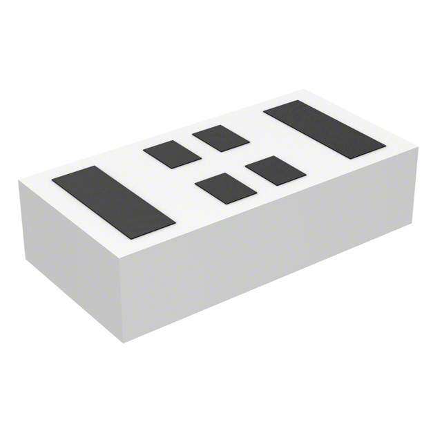
| 尺寸 | 3.2 mm L x 1.6 mm W x 0.5 mm H |
| 技术类型 | High Efficiency Loop Antenna |
| 标准包装 | 1 |
| 端接 | 表面贴装型 |
| 端接类型 | SMD/SMT |
| 长度 | 3.2 mm |
| 阻抗 | 50 Ohms |
| 频带数 | 1 |
| 频率 | 2.4 GHz |
| 高度 | 0.5 mm |
| 高度(最大值) | 0.020"(0.50mm) |


- 商务部:美国ITC正式对集成电路等产品启动337调查
- 曝三星4nm工艺存在良率问题 高通将骁龙8 Gen1或转产台积电
- 太阳诱电将投资9.5亿元在常州建新厂生产MLCC 预计2023年完工
- 英特尔发布欧洲新工厂建设计划 深化IDM 2.0 战略
- 台积电先进制程称霸业界 有大客户加持明年业绩稳了
- 达到5530亿美元!SIA预计今年全球半导体销售额将创下新高
- 英特尔拟将自动驾驶子公司Mobileye上市 估值或超500亿美元
- 三星加码芯片和SET,合并消费电子和移动部门,撤换高东真等 CEO
- 三星电子宣布重大人事变动 还合并消费电子和移动部门
- 海关总署:前11个月进口集成电路产品价值2.52万亿元 增长14.8%
PDF Datasheet 数据手册内容提取
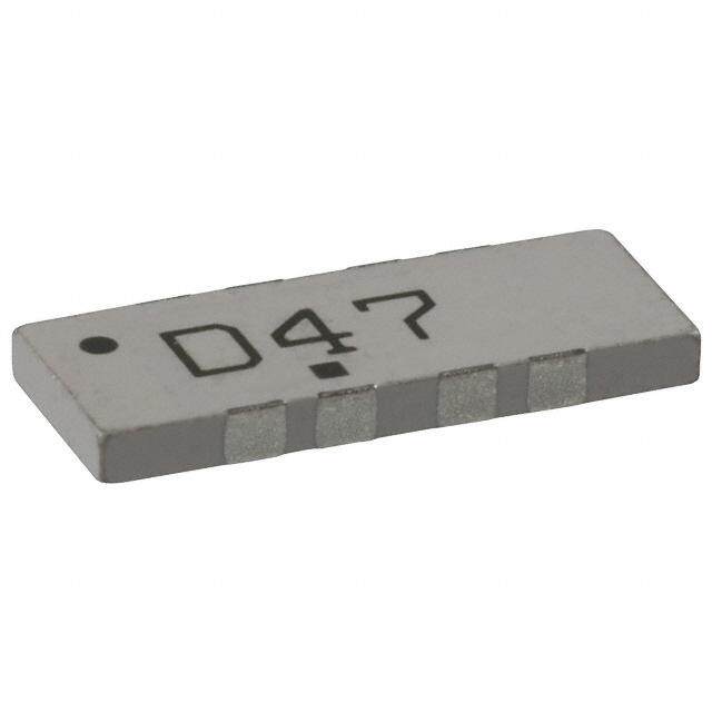
Specification Part No. : WLA.01 Model : 2.4GHz High Efficiency Loop Antenna Description : 2.5dBi 2400MHz to 2500MHz WLAN/WIFI/Bluetooth/Zigbee Features : 3.2*1.6*0.5mm Low Profile Peak gain 2.5dBi 50 Ohm Impedance RoHS Compliant SPE-11-8-146/K/SS Page 1 of 18
1. Introduction The WLA.01 2.4GHz Loop antenna is a high efficiency, miniature SMD, edge mounted ceramic antenna for very small space requirements for Wi-Fi, WLAN, Zigbee, Bluetooth, and 802.11 applications. The WLA.01 uses the main PCB as its ground plane, thereby increasing Antenna Efficiency. It is tuned for different PCB sizes by simply changing the value of the matching circuit. At 3.2mm*1.6mm*0.5mm, the WLA.01 is one of the smallest antennas available worldwide. This antenna is delivered on tape and Reel. Many module manufacturers specify peak gain limits for any antennas that are to be connected to that module. Those peak gain limits are based on free-space conditions. In practice, the peak gain of an antenna tested in free-space can degrade by at least 1 or 2dBi when put inside a device. So ideally you should go for a slightly higher peak gain antenna than mentioned on the module specification to compensate for this effect, giving you better performance. Upon testing of any of our antennas with your device and a selection of appropriate layout, integration technique, or cable, Taoglas can make sure any of our antennas’ peak gain will be below the peak gain limits. Taoglas can then issue a specification and/or report for the selected antenna in your device that will clearly show it complying with the peak gain limits, so you can be assured you are meeting regulatory requirements for that module. For example, a module manufacturer may state that the antenna must have less than 2dBi peak gain, but you don’t need to select an embedded antenna that has a peak gain of less than 2dBi in free-space. This will give you a less optimized solution. It is better to go for a slightly higher free-space peak gain of 3dBi or more if available. Once that antenna gets integrated into your device, performance will degrade below this 2dBi peak gain due to the effects of GND plane, surrounding components, and device housing. If you want to be absolutely sure, contact Taoglas and we will test. Choosing a Taoglas antenna with a higher peak gain than what is specified by the module manufacturer and enlisting our help will ensure you are getting the best performance possible without exceeding the peak gain limits. SPE-11-8-146/K/SS Page 2 of 18
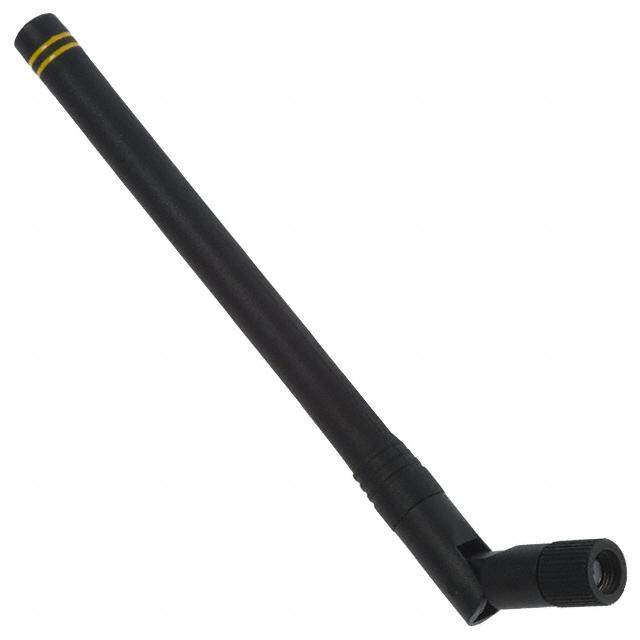
1.1 Applications *Bluetooth earphone systems *Hand-held devices when Bluetooth/Wi-Fi functions are needed, e.g., Smart phone. *IEEE802.11 b/g *ZigBee *Wireless PCMCIA cards or USB dongle SPE-11-8-146/K/SS Page 3 of 18
2. Specifications The WLA.01 is designed to mount at the center of the edge of an evaluation board of 80 x 40mm.The antenna performance was measured with the WLA.01 mounted on the evaluation board with SMA(F) connector. No Parameter Specification* 1 Center Frequency 2400-2500MHz 2 Dimensions 3.2*1.6*0.5mm 3 VSWR 2 max 4 Polarization Linear 5 Bandwidth 100MHz min. 6 Gain Peak 2.5dBi typ. 7 Efficiency 84% typ. 8 Impedance 50 Mechanical 9 Dimensions 3.2*1.6*0.5mm 10 Material Ceramic Environmental 11 Operating Temperature -40°C+85°C 12 Storage Temperature -40°C+105°C 13 Temperature Coefficient(τf) 0 20 ppm @-20ºC to +80ºC Recommended Reel Storage 5°C to 40°C 14 Condition Relative Humidity 20% to 70% * The data was measured by a CTIA Authorized Test Lab. ** Center frequency will be offset to working frequency according to the conditions of user’s Ground plane and radome. SPE-11-8-146/K/SS Page 4 of 18
3. Electrical Specification (80*40mm ground plane) 3.1 Return Loss(S11) SPE-11-8-146/K/SS Page 5 of 18
3.2 VSWR SPE-11-8-146/K/SS Page 6 of 18
4. Radiation Pattern (Customize Design) SPE-11-8-146/K/SS Page 7 of 18
4.1 Radiation Pattern (80mmX40mm ground plane) Z X Y 4.2 3D Gain pattern @2442MHz SPE-11-8-146/K/SS Page 8 of 18
5.1 3D Gain Pattern SPE-11-8-146/K/SS Page 9 of 18
4.3 Efficiency Table 4.4 Efficiency vs Frequency SPE-11-8-146/K/SS Page 10 of 18
5. Layout Guide 5.1 Solder Land Pattern Land pattern for soldering (grey marking areas) is as shown below. A matching circuit similar to the one shown in section 5.3 is also required. SPE-11-8-146/K/SS Page 11 of 18
SPE-11-8-146/K/SS Page 12 of 18
5.2 Solder Land Pattern This antenna includes a fine tuning element (as shown in the land patterns above) that can be used to slightly shift antenna resonance. 5.3 Matching Circuit Like all antennas, surrounding components, enclosures, and changes to the GND plane dimensions can alter performance. A pi-matching network like the one shown below is required in case adjustments need to be made. The antenna EVB has a similar matching network. The components on the EVB are a good starting point for a new design, but will need to be adjusted upon integration for best performance. The zero ohm resistor is needed for the ability to solder down a coax pigtail to make measurements with a vector network analyzer. SPE-11-8-146/K/SS Page 13 of 18
6. Antenna Drawings 6.1 Antenna Main Body SPE-11-8-146/K/SS Page 14 of 18
6.2 Antenna with EVB 6.3 Footprint on EVB SPE-11-8-146/K/SS Page 15 of 18
7. Packaging SPE-11-8-146/K/SS Page 16 of 18
7.1 Tape Dimensions (unit: mm) Feature Specifications Tolerances W 12 ±0.30 P 8 ±0.10 E 1.75 ±0.10 F 5.5 ±0.10 P2 2 ±0.10 D 1.5 ±0.10 Po 4 ±0.10 10Po 40 ±0.20 7.2 Pocket Dimensions (unit: mm) Feature Specifications Tolerances Ao 1.9 ±0.10 Bo 3.5 ±0.10 Ko 0.8 ±0.10 t 0.3 ±0.05 SPE-11-8-146/K/SS Page 17 of 18
8. Recommended Reflow Temp Profile The WLA.01 Loop Antenna can be assembled following either Sn-Pb or Pb-Free assembly processes. The recommended soldering temperatures are as follows: SPE-11-8-146/K/SS Page 18 of 18