首页 > VRF151 > 详情
 Datasheet下载
- 型号: VRF151
- 制造商: American Microsemiconductor, Inc.
- 库位|库存: xxxx|xxxx
- 要求:
| 数量阶梯 | 香港交货 | 国内含税 |
| +xxxx | $xxxx | ¥xxxx |
查看当月历史价格
查看今年历史价格
产品参数
| 参数 | 数值 |
| 产品目录 | 分立半导体产品 |
| 描述 | MOSFET RF PWR N-CH 50V 150W M174 |
| 产品分类 | RF FET |
| 品牌 | Microsemi Power Products Group |
| 数据手册 | http://www.microsemi.com/document-portal/doc_download/77331-vrf151-mp-f-pdfhttp://www2.microsemi.com/document-portal/doc_download/14813-power-products-group-ppg-catalog |
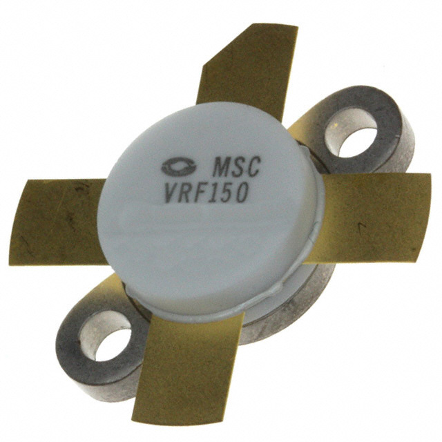
| 产品图片 |  |
| 产品型号 | VRF151 |
| rohs | 无铅 / 符合限制有害物质指令(RoHS)规范要求 |
| 产品系列 | - |
| 产品目录页面 | 点击此处下载产品Datasheet |
| 供应商器件封装 | M174 |
| 其它名称 | VRF151MP VRF151MP-ND |
| 功率-输出 | 150W |
| 包装 | 管件 |
| 噪声系数 | - |
| 增益 | 22dB |
| 封装/外壳 | M174 |
| 晶体管类型 | N 通道 |
| 标准包装 | 30 |
| 特色产品 | http://www.digikey.com/cn/zh/ph/microsemi/vrf15x.html |
| 电压-测试 | 50V |
| 电压-额定 | 170V |
| 电流-测试 | 250mA |
| 频率 | 30MHz |
| 额定电流 | 16A |
Datasheet
PDF Datasheet 数据手册内容提取
VRF151 VRF151MP 50V, 150W, 175MHz RF POWER VERTICAL MOSFET The VRF151 is a gold-metallized silicon n-channel RF power transistor de- signed for broadband commercial and military applications requiring high power and gain without compromising reliability, ruggedness, or inter-modulation distortion. M174 FEATURES • Improved Ruggedness V = 170V • 70:1 Load VSWR Capability at Specified Operating Conditions (BR)DSS • 150W with 22dB Typical Gain @ 30MHz, 50V • Nitride Passivated • 150W with 14dB Typical Gain @ 175MHz, 50V • Refractory Gold Metallization • Excellent Stability & Low IMD • High Voltage Replacement for MRF151 • Common Source Configuration • RoHS Compliant • Available in Matched Pairs Maximum Ratings All Ratings: T =25°C unless otherwise specified C Symbol Parameter VRF151(MP) Unit VDSS Drain-Source Voltage 170 V ID Continuous Drain Current @ TC = 25°C 16 A VGS Gate-Source Voltage ±40 V PD Total Device dissipation @ TC = 25°C 300 W TSTG Storage Temperature Range -65 to 150 °C TJ Operating Junction Temperature 200 Static Electrical Characteristics Symbol Parameter Min Typ Max Unit V(BR)DSS Drain-Source Breakdown Voltage (VGS = 0V, ID = 100mA) 170 180 V VDS(ON) On State Drain Voltage (ID(ON) = 10A, VGS = 10V) 2.0 3.0 I Zero Gate Voltage Drain Current (V = 100V, V = 0V) 1 mA DSS DS GS I Gate-Source Leakage Current (V = ±20V, V = 0V) 1.0 μA GSS GS DS g Forward Transconductance (V = 10V, I = 5A) 5.0 mhos fs DS D V Gate Threshold Voltage (V = 10V, I = 100mA) 2.9 3.6 4.4 V GS(TH) DS D Thermal Characteristics Symbol Characteristic Min Typ Max Unit R Junction to Case Thermal Resistance 0.60 °C/W θJC 3 1 0 2 CAUTION: These Devices are Sensitive to Electrostatic Discharge. Proper Handling Procedures Should Be Followed. 12- G ev R 7 3 9 Microsemi Website - http://www.microsemi.com 0-4 5 0
Dynamic Characteristics VRF151(MP) Symbol Parameter Test Conditions Min Typ Max Unit C Input Capacitance V = 0V 375 ISS GS C Output Capacitance V = 150V 200 pF oss DS C Reverse Transfer Capacitance f = 1MHz 12 rss Functional Characteristics Symbol Parameter Min Typ Max Unit G f = 30MHz, f = 30.001MHz, V = 50V, I = 250mA, P = 150W 1 18 22 PS 1 2 DD DQ out PEP dB G f = 175MHz, V = 50V, I = 250mA, P = 150W 14 PS DD DQ out ηD f 1= 30MHz, f2 = 30.001MHz, VDD = 50V, IDQ = 250mA, Pout = 150WPEP 1 50 % IMD f = 30MHz, f = 30.001MHz, V = 50V, I = 250mA, P = 150W 1 -30 dBc (d3) 1 2 DD DQ out PEP f = 50MHz, V = 50V, I = 250mA, P = 150WCW ψ 1 DD DQ out No Degradation in Output Power 70:1 VSWR - All Phase Angles , 0.2mSec X 20% Duty Factor 1. To MIL-STD-1311 Version A, test method 2204B, Two Tone, Reference Each Tone Microsemi reserves the right to change, without notice, the specifications and information contained herein. Typical Performance Curves 25 30 14V 250µs PULSE TEST<0.5 % DUTY 10V CYCLE 25 20 9V T= -55°C J A) A) 20 ENT ( 15 8V 7V ENT ( TJ= 25°C R R 15 R R T= 125°C U 6V U J C 10 C AIN AIN 10 R R D 5V D , D 5 , D 5 I I 4V 0 0 0 4 8 12 16 20 0 2 4 6 8 10 12 V , DRAIN-TO-SOURCE VOLTAGE (V) V , GATE-TO-SOURCE VOLTAGE (V) DS(ON) GS FIGURE 1, Output Characteristics FIGURE 2, Transfer Characteristics 100 20 Ciss 10 I Pdmax DMax ACITANCE (pF) 10 Coss N CURRENT (V) 1 Rds(on) DC line P AI A R C D C, , D 3 I 12-201 Crss TTJC = = 1 7255°°CC G 1 0.1 ev 0 10 20 30 40 50 1 10 100 250 R 7 VDS, DRAIN-TO-SOURCE VOLTAGE (V) VDS, DRAIN-TO-SOURCE VOLTAGE (V) 93 FIGURE 3, Capacitance vs Drain-to-Source Voltage FIGURE 4, Forward Safe Operating Area 4 0- 5 0
Typical Performance Curves VRF151(MP) 0.7 W) 0.6 C/ 0.9 E (° 0.5 C N 0.7 A ED 0.4 P M L I 0.3 0.5 Note: ERMA 0.2 0.3 PDM t1 H t2 , TθJC 0.1 0.1 Dtu1t =y FPauclstoe rD Du =rat iot1n/t2 Z 0.05 SINGLE PULSE Peak TJ = PDM x ZθJC + TC 0 10-5 10-4 10-3 10-2 10 - 1 1.0 RECTANGULAR PULSE DURATION (seconds) Figure 5. Maximum Effective Transient Thermal Impedance Junction-to-Case vs Pulse Duration -20 B) 250 N (d -25 Vdd=F5r0eVq,= I1d5q0 =M 2H5z0mA, IM3 Vdd=F5r0eVq,= I1d5q0 =M 2H5z0mA, Vdd=50V O TI -30 200 ON DISTOR --4305 IM5 WER (W)PEP 150 Vdd=40V ATI PO UL -45 UT 100 D P MO -50 UT R O E 50 T -55 N MD, I -60 I 0 50 100 150 200 0 0 5 10 15 20 25 30 P , OUTPUT POWER (WATTS PEP) P , INPUT POWER (WATTS PEP) out out Figure 6. IMD versus POUT Figure 7. POUT versus PIN 3 1 0 2 2- 1 G ev R 7 3 9 4 0- 5 0
VRF151(MP) 30 MHz test Circuit + 50VDC L1 + L2 Bias C6 C7 C8 C9 C10 0-12V C5 T2 RF R1 Output DUT C4 R3 C2 C3 RF R2 Input C1 L1 - VK200-4B C1 -- 470 pF Dipped Mica L2 -- 2 Ferrite beads, 2.0 uH C2, C5, C6 - C9 -- 0.1uF SMT R1, R2 -- 51 (cid:55), 1 W Carbon C3 -- 200pF ATC 700C R3 -- 3.3 (cid:55), 1 W Carbon C4 -- 15pF, ATC 700C T1 -- 9:1 Transformer C10 -- 10uF, 100V Electrolytic T2 -- 1:9 Transformer 175 MHz test Circuit RFC1 + 50VDC + L4 C10 C11 Bias 0-12V + RF R1 L2 L3 C9 Output C4 C5 R3 C1 C6 C7 C8 RF Input L1 DUT C3 C2 R2 C1, C2, C8 -- Arco 463 or equivalent C3 -- 25pF, Unelco C4 -- 0.1uF, Ceramic C5 -- 1.0 uF, 15 WV Tantalum C6 -- 250pF, Unelco J101 C7-- 25pF, Unelco J101 13 C9 -- Arco 262 or equivalent 0 2-2 C10 -- 0.05uF, Ceramic 1 G C11 -- 15uF, 60WV Electrolytic ev R 7 3 9 4 0- 5 0
VRF151(MP) Adding MP at the end of P/N specifies a matched pair where V is matched between the two parts. V values GS(TH) TH are marked on the devices per the following table. Code Vth Range Code 2 Vth Range A 2.900 - 2.975 M 3.650 - 3.725 B 2.975 - 3.050 N 3.725 - 3.800 C 3.050 - 3.125 P 3.800 - 3.875 D 3.125 - 3.200 R 3.875 - 3.950 E 3.200 - 3.275 S 3.950 - 4.025 F 3.275 - 3.350 T 4.025 - 4.100 G 3.350 - 3.425 W 4.100 - 4.175 H 3.425 - 3.500 X 4.175 - 4.250 J 3.500 - 3.575 Y 4.250 - 4.325 K 3.575 - 3.650 Z 4.325 - 4.400 V values are based on Microsemi measurements at datasheet conditions with an accuracy of 1.0%. TH .5” SOE Package Outline All Dimensions are ± .005 A U M INCHES MILLIMETERS DIM MIN MAX MIN MAX 1 M Q A 0.096 0.990 24.39 25.14 4 B 0.465 0.510 11.82 12.95 C 0.229 0.275 5.82 6.98 R B D 0.216 0.235 5.49 5.96 E 0.084 0.110 2.14 2.79 PIN 1 - SOURCE PIN 2 - GATE 2 3 H 0.144 0.178 3.66 4.52 PIN 3 - SOURCE D J 0.003 0.007 0.08 0.17 PIN 4 - DRAIN K K 0.435 11.0 M 45° NOM 45° NOM J Q 0.115 0.130 2.93 3.30 R 0.246 0.255 6.25 6.47 C H E U 0.720 0.730 18.29 18.54 Seating Plane 3 1 0 2 2- 1 G ev R 7 3 9 4 0- 5 0
VRF151(MP) The information contained in the document (unless it is publicly available on the Web without access restrictions) is PROPRIETARY AND CONFI- DENTIAL information of Microsemi and cannot be copied, published, uploaded, posted, transmitted, distributed or disclosed or used without the express duly signed written consent of Microsemi. If the recipient of this document has entered into a disclosure agreement with Microsemi, then the terms of such Agreement will also apply . This document and the information contained herein may not be modified, by any person other than authorized personnel of Microsemi. No license under any patent, copyright, trade secret or other intellectual property right is granted to or conferred upon you by disclosure or delivery of the information, either expressly, by implication, inducement, estoppels or otherwise. Any license under such intellectual property rights must be approved by Microsemi in writing signed by an officer of Microsemi. Microsemi reserves the right to change the configuration, functionality and performance of its products at anytime without any notice. This prod- uct has been subject to limited testing and should not be used in conjunction with life-support or other mission-critical equipment or applications. Microsemi assumes no liability whatsoever, and Microsemi disclaims any express or implied warranty, relating to sale and/or use of Microsemi products including liability or warranties relating to fitness for a particular purpose, merchantability, or infringement of any patent, copyright or other intellectual property right. Any performance specifications believed to be reliable but are not verified and customer or user must conduct and complete all performance and other testing of this product as well as any user or customers final application. User or customer shall not rely 3 on any data and performance specifications or parameters provided by Microsemi. It is the customer’s and user’s responsibility to independently 1 0 2-2 determine suitability of any Microsemi product and to test and verify the same. The information contained herein is provided “AS IS, WHERE IS” 1 G and with all faults, and the entire risk associated with such information is entirely with the User. Microsemi specifically disclaims any liability of any Rev kind including for consequential, incidental and punitive damages as well as lost profit. The product is subject to other terms and conditions which 37 can be located on the web at http://www.microsemi.com/legal/tnc.asp 9 4 0- 5 0