ICGOO在线商城 > 集成电路(IC) > PMIC - 配电开关,负载驱动器 > VNL5090N3TR-E
 Datasheet下载
- 型号: VNL5090N3TR-E
- 制造商: STMicroelectronics
- 库位|库存: xxxx|xxxx
- 要求:
| 数量阶梯 | 香港交货 | 国内含税 |
| +xxxx | $xxxx | ¥xxxx |
查看当月历史价格
查看今年历史价格
VNL5090N3TR-E产品简介:
ICGOO电子元器件商城为您提供VNL5090N3TR-E由STMicroelectronics设计生产,在icgoo商城现货销售,并且可以通过原厂、代理商等渠道进行代购。 VNL5090N3TR-E价格参考。STMicroelectronicsVNL5090N3TR-E封装/规格:PMIC - 配电开关,负载驱动器, 。您可以下载VNL5090N3TR-E参考资料、Datasheet数据手册功能说明书,资料中有VNL5090N3TR-E 详细功能的应用电路图电压和使用方法及教程。
STMicroelectronics的VNL5090N3TR-E是一款PMIC(电源管理集成电路)中的配电开关和负载驱动器,广泛应用于需要高效电源管理和驱动能力的场景。以下是该型号的主要应用场景:

 1. 汽车电子
   - LED驱动:用于驱动汽车内部和外部的LED灯(如尾灯、刹车灯、转向灯等),提供稳定电流输出。
   - 电机控制:适用于小型直流电机的驱动,例如车窗升降、座椅调节或雨刷系统。
   - 传感器供电:为车载传感器(如压力、温度或位置传感器)提供精确的电源管理。

 2. 工业自动化
   - 设备电源管理:在工业设备中,用于管理不同模块的电源分配,确保各部分按需供电。
   - 负载切换:在多负载系统中实现快速切换,避免过载或短路对系统的影响。

 3. 消费电子
   - 便携式设备:为智能音箱、游戏控制器或其他便携式设备中的小型电机或灯光提供驱动。
   - 智能家居:用于驱动智能灯具、窗帘电机或家电中的小型执行器。

 4. 通信与网络设备
   - 信号指示灯:驱动路由器、交换机等设备上的状态指示灯。
   - 风扇控制:为散热风扇提供稳定的驱动电流,确保设备冷却系统的正常运行。

 5. 医疗设备
   - 小型泵驱动:在便携式医疗设备(如胰岛素泵)中,用于驱动小型泵或电机。
   - 显示屏背光:为医疗监测设备的显示屏提供稳定的背光驱动。

 特点总结
- 高效率:支持低功耗设计,适合电池供电的应用。
- 保护功能:内置过流、过温保护,提高系统可靠性。
- 紧凑封装:节省空间,便于集成到小型化设计中。

VNL5090N3TR-E凭借其高性能和可靠性,成为多种应用领域的理想选择,尤其在汽车电子和工业自动化领域表现突出。
| 参数 | 数值 |
| 产品目录 | 集成电路 (IC) |
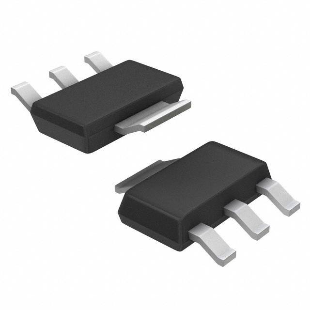
| 描述 | IC DVR LOW SIDE OMINIFET SOT-223 |
| 产品分类 | PMIC - MOSFET,电桥驱动器 - 内部开关 |
| 品牌 | STMicroelectronics |
| 数据手册 | |
| 产品图片 |
|
| 产品型号 | VNL5090N3TR-E |
| rohs | 无铅 / 符合限制有害物质指令(RoHS)规范要求 |
| 产品系列 | OMNIFET III™, VIPower™ |
| 产品培训模块 | http://www.digikey.cn/PTM/IndividualPTM.page?site=cn&lang=zhs&ptm=26261 |
| 供应商器件封装 | SOT-223 |
| 其它名称 | 497-14326-1 |
| 其它有关文件 | http://www.st.com/web/catalog/sense_power/FM1965/CL1969/SC1038/PF251647?referrer=70071840 |
| 包装 | 剪切带 (CT) |
| 安装类型 | 表面贴装 |
| 导通电阻 | 90 毫欧 |
| 封装/外壳 | TO-261-4,TO-261AA |
| 工作温度 | -40°C ~ 150°C |
| 标准包装 | 1 |
| 电压-电源 | 3.5 V ~ 5.5 V |
| 电流-峰值输出 | - |
| 电流-输出/通道 | 13A |
| 类型 | 低端 |
| 输入类型 | 非反相 |
| 输出数 | 1 |


PDF Datasheet 数据手册内容提取
VNL5090N3-E, VNL5090S5-E OMNIFET III fully protected low side driver for automotive applications Datasheet - production data Description 2 The VNL5090N3-E and VNL5090S5-E are monolithic devices made using 3 2 STMicroelectronics® VIPower® technology, 1 intended for driving resistive or inductive loads SOT-223 SO-8 with one side connected to the battery. Built-in thermal shutdown protects the chip from overtemperature and short-circuit. Features Output current limitation protects the devices in an overload condition. In case of long duration Type V R I overload, the device limits the dissipated power to clamp DS(on) D a safe level up to thermal shutdown VNL5090N3-E intervention.Thermal shutdown, with automatic 4 1V 90m 1 3A VNL5090S5-E restart, allows the devices to recover normal operation as soon as a fault condition disappears. Fast demagnetization of inductive loads is AEC-Q100 qualified achieved at turn-off. D rain current: 13A ESD protection Overvoltage clamp Thermal shutdown Current and power limitation Very low standby current Very low electromagnetic susceptibility Compliant with European directive 2002/95/EC Open drain status output (VNL5090S5-E only) S pecially intended for 2 x R10W or 4 xR5W automotive signal lamps Table 1. Devices summary Order codes Package Tube Tape and reel SOT-223 VNL5090N3-E VNL5090N3TR-E SO-8 VNL5090S5-E VNL5090S5TR-E November 2018 DS8791 Rev 8 1/28 This is information on a product in full production. www.st.com
Contents VNL5090N3-E, VNL5090S5-E Contents 1 Block diagrams and pins configurations . . . . . . . . . . . . . . . . . . . . . . . . 5 2 Electrical specifications . . . . . . . . . . . . . . . . . . . . . . . . . . . . . . . . . . . . . . 8 2.1 Absolute maximum ratings . . . . . . . . . . . . . . . . . . . . . . . . . . . . . . . . . . . . . 8 2.2 Thermal data . . . . . . . . . . . . . . . . . . . . . . . . . . . . . . . . . . . . . . . . . . . . . . . 8 2.3 Electrical characteristics . . . . . . . . . . . . . . . . . . . . . . . . . . . . . . . . . . . . . . . 9 3 Application information . . . . . . . . . . . . . . . . . . . . . . . . . . . . . . . . . . . . . 13 3.1 MCU I/O protection . . . . . . . . . . . . . . . . . . . . . . . . . . . . . . . . . . . . . . . . . . 14 4 Package and PC board thermal data . . . . . . . . . . . . . . . . . . . . . . . . . . . 16 4.1 SOT-223 thermal data . . . . . . . . . . . . . . . . . . . . . . . . . . . . . . . . . . . . . . . 16 4.2 SO-8 thermal data . . . . . . . . . . . . . . . . . . . . . . . . . . . . . . . . . . . . . . . . . . 19 5 Package and packing information . . . . . . . . . . . . . . . . . . . . . . . . . . . . . 22 5.1 SOT-223 mechanical data . . . . . . . . . . . . . . . . . . . . . . . . . . . . . . . . . . . . 22 5.2 SO-8 mechanical data . . . . . . . . . . . . . . . . . . . . . . . . . . . . . . . . . . . . . . . 23 5.3 SOT-223 packing information . . . . . . . . . . . . . . . . . . . . . . . . . . . . . . . . . . 25 5.4 SO-8 packing information . . . . . . . . . . . . . . . . . . . . . . . . . . . . . . . . . . . . . 26 6 Revision history . . . . . . . . . . . . . . . . . . . . . . . . . . . . . . . . . . . . . . . . . . . 27 2/28 DS8791 Rev 8
VNL5090N3-E, VNL5090S5-E List of tables List of tables Table 1. Devices summary. . . . . . . . . . . . . . . . . . . . . . . . . . . . . . . . . . . . . . . . . . . . . . . . . . . . . . . . .1 Table 2. Pin function. . . . . . . . . . . . . . . . . . . . . . . . . . . . . . . . . . . . . . . . . . . . . . . . . . . . . . . . . . . . . .6 Table 3. Suggested connections for unused and N.C. pins . . . . . . . . . . . . . . . . . . . . . . . . . . . . . . . .7 Table 4. Absolute maximum ratings . . . . . . . . . . . . . . . . . . . . . . . . . . . . . . . . . . . . . . . . . . . . . . . . . .8 Table 5. Thermal data. . . . . . . . . . . . . . . . . . . . . . . . . . . . . . . . . . . . . . . . . . . . . . . . . . . . . . . . . . . . .8 Table 6. PowerMOS section. . . . . . . . . . . . . . . . . . . . . . . . . . . . . . . . . . . . . . . . . . . . . . . . . . . . . . . .9 Table 7. Source drain diode . . . . . . . . . . . . . . . . . . . . . . . . . . . . . . . . . . . . . . . . . . . . . . . . . . . . . . . .9 Table 8. Input section (VNL5090N3-E only). . . . . . . . . . . . . . . . . . . . . . . . . . . . . . . . . . . . . . . . . . . .9 Table 9. Status pin (VNL5090S5-E only) . . . . . . . . . . . . . . . . . . . . . . . . . . . . . . . . . . . . . . . . . . . . . .9 Table 10. Logic input (VNL5090S5-E only). . . . . . . . . . . . . . . . . . . . . . . . . . . . . . . . . . . . . . . . . . . . .10 Table 11. Openload detection (VNL5090S5-E only). . . . . . . . . . . . . . . . . . . . . . . . . . . . . . . . . . . . . .10 Table 12. Supply section (VNL5090S5-E only). . . . . . . . . . . . . . . . . . . . . . . . . . . . . . . . . . . . . . . . . .10 Table 13. Switching characteristics. . . . . . . . . . . . . . . . . . . . . . . . . . . . . . . . . . . . . . . . . . . . . . . . . . .11 Table 14. Protection and diagnostics . . . . . . . . . . . . . . . . . . . . . . . . . . . . . . . . . . . . . . . . . . . . . . . . .11 Table 15. Truth table (VNL5090S5-E only). . . . . . . . . . . . . . . . . . . . . . . . . . . . . . . . . . . . . . . . . . . . .12 Table 16. SOT-223 thermal parameters. . . . . . . . . . . . . . . . . . . . . . . . . . . . . . . . . . . . . . . . . . . . . . .18 Table 17. SO-8 thermal parameters. . . . . . . . . . . . . . . . . . . . . . . . . . . . . . . . . . . . . . . . . . . . . . . . . .21 Table 18. SOT-223 mechanical data . . . . . . . . . . . . . . . . . . . . . . . . . . . . . . . . . . . . . . . . . . . . . . . . .23 Table 19. SO-8 mechanical data . . . . . . . . . . . . . . . . . . . . . . . . . . . . . . . . . . . . . . . . . . . . . . . . . . . .24 Table 20. Document revision history. . . . . . . . . . . . . . . . . . . . . . . . . . . . . . . . . . . . . . . . . . . . . . . . . .27 DS8791 Rev 8 3/28 3
List of figures VNL5090N3-E, VNL5090S5-E List of figures Figure 1. VNL5090N3-E block diagram. . . . . . . . . . . . . . . . . . . . . . . . . . . . . . . . . . . . . . . . . . . . . . . .5 Figure 2. VNL5090S5-E block diagram . . . . . . . . . . . . . . . . . . . . . . . . . . . . . . . . . . . . . . . . . . . . . . . .5 Figure 3. VNL5090N3-E current and voltage conventions. . . . . . . . . . . . . . . . . . . . . . . . . . . . . . . . . .6 Figure 4. VNL5090S5-E current and voltage conventions . . . . . . . . . . . . . . . . . . . . . . . . . . . . . . . . .6 Figure 5. Configuration diagrams (top view) . . . . . . . . . . . . . . . . . . . . . . . . . . . . . . . . . . . . . . . . . . . .7 Figure 6. Switching characteristics. . . . . . . . . . . . . . . . . . . . . . . . . . . . . . . . . . . . . . . . . . . . . . . . . . .12 Figure 7. VNL5090N3-E application schematic. . . . . . . . . . . . . . . . . . . . . . . . . . . . . . . . . . . . . . . . .13 Figure 8. VNL5090S5-E application schematic . . . . . . . . . . . . . . . . . . . . . . . . . . . . . . . . . . . . . . . . .13 Figure 9. Maximum demagnetization energy (V = 16 V). . . . . . . . . . . . . . . . . . . . . . . . . . . . . . . .15 CC Figure 10. SOT-223 PC board. . . . . . . . . . . . . . . . . . . . . . . . . . . . . . . . . . . . . . . . . . . . . . . . . . . . . . .16 Figure 11. SOT-223 Rthj-amb vs PCB copper area in open box free air condition. . . . . . . . . . . . . . .16 Figure 12. SOT-223 thermal impedance junction ambient single pulse. . . . . . . . . . . . . . . . . . . . . . . .17 Figure 13. Thermal fitting model of a LSD in SOT-223 . . . . . . . . . . . . . . . . . . . . . . . . . . . . . . . . . . . .17 Figure 14. SO-8 PC board. . . . . . . . . . . . . . . . . . . . . . . . . . . . . . . . . . . . . . . . . . . . . . . . . . . . . . . . . .19 Figure 15. SO-8 Rthj-amb vs PCB copper area in open box free air condition . . . . . . . . . . . . . . . . . .19 Figure 16. SO-8 thermal impedance junction ambient single pulse. . . . . . . . . . . . . . . . . . . . . . . . . . .20 Figure 17. Thermal fitting model of a LSD in SO-8 . . . . . . . . . . . . . . . . . . . . . . . . . . . . . . . . . . . . . . .20 Figure 18. SOT-223 package dimensions . . . . . . . . . . . . . . . . . . . . . . . . . . . . . . . . . . . . . . . . . . . . . .22 Figure 19. SO-8 package dimensions . . . . . . . . . . . . . . . . . . . . . . . . . . . . . . . . . . . . . . . . . . . . . . . . .23 Figure 20. SOT-223 tape and reel shipment (suffix “TR”) . . . . . . . . . . . . . . . . . . . . . . . . . . . . . . . . . .25 Figure 21. SO-8 tube shipment (no suffix). . . . . . . . . . . . . . . . . . . . . . . . . . . . . . . . . . . . . . . . . . . . . .26 Figure 22. SO-8 tape and reel shipment (suffix “TR”) . . . . . . . . . . . . . . . . . . . . . . . . . . . . . . . . . . . . .26 4/28 DS8791 Rev 8
VNL5090N3-E, VNL5090S5-E Block diagrams and pins configurations 1 Block diagrams and pins configurations Figure 1. VNL5090N3-E block diagram (cid:39)(cid:53)(cid:36)(cid:44)(cid:49) (cid:47)(cid:50)(cid:42)(cid:44)(cid:38) (cid:38)(cid:82)(cid:81)(cid:87)(cid:85)(cid:82)(cid:79)(cid:3)(cid:9)(cid:3)(cid:39)(cid:76)(cid:68)(cid:74)(cid:81)(cid:82)(cid:86)(cid:87)(cid:76)(cid:70) (cid:38)(cid:88)(cid:85)(cid:85)(cid:72)(cid:81)(cid:87)(cid:3) (cid:51)(cid:82)(cid:90)(cid:72)(cid:85)(cid:3) (cid:47)(cid:76)(cid:80)(cid:76)(cid:87)(cid:68)(cid:87)(cid:76)(cid:82)(cid:81) (cid:38)(cid:79)(cid:68)(cid:80)(cid:83) (cid:44)(cid:49)(cid:51)(cid:56)(cid:55) (cid:39)(cid:53)(cid:44)(cid:57)(cid:40)(cid:53) (cid:50)(cid:57)(cid:40)(cid:53)(cid:55)(cid:40)(cid:48)(cid:51)(cid:40)(cid:53)(cid:36)(cid:55)(cid:56)(cid:53)(cid:40)(cid:3) (cid:51)(cid:53)(cid:50)(cid:55)(cid:40)(cid:38)(cid:55)(cid:44)(cid:50)(cid:49) (cid:50)(cid:57)(cid:40)(cid:53)(cid:47)(cid:50)(cid:36)(cid:39)(cid:3)(cid:51)(cid:53)(cid:50)(cid:55)(cid:40)(cid:38)(cid:55)(cid:44)(cid:50)(cid:49) (cid:11)(cid:36)(cid:38)(cid:55)(cid:44)(cid:57)(cid:40)(cid:3)(cid:51)(cid:50)(cid:58)(cid:40)(cid:53)(cid:3)(cid:47)(cid:44)(cid:48)(cid:44)(cid:55)(cid:36)(cid:55)(cid:44)(cid:50)(cid:49)(cid:12) (cid:42)(cid:49)(cid:39) (cid:40)(cid:34)(cid:49)(cid:40)(cid:36)(cid:39)(cid:53)(cid:17)(cid:17)(cid:23)(cid:20)(cid:17) Figure 2. VNL5090S5-E block diagram (cid:39)(cid:53)(cid:36)(cid:44)(cid:49) (cid:54)(cid:56)(cid:51)(cid:51)(cid:47)(cid:60) (cid:54)(cid:56)(cid:51)(cid:51)(cid:47)(cid:60) (cid:38)(cid:82)(cid:81)(cid:87)(cid:85)(cid:82)(cid:79)(cid:3)(cid:9)(cid:3)(cid:39)(cid:76)(cid:68)(cid:74)(cid:81)(cid:82)(cid:86)(cid:87)(cid:76)(cid:70) (cid:57)(cid:50)(cid:47)(cid:55)(cid:36)(cid:42)(cid:40) (cid:50)(cid:41)(cid:41)(cid:3)(cid:54)(cid:87)(cid:68)(cid:87)(cid:72)(cid:3) (cid:47)(cid:50)(cid:42)(cid:44)(cid:38) (cid:50)(cid:83)(cid:72)(cid:81)(cid:3)(cid:79)(cid:82)(cid:68)(cid:71) (cid:38)(cid:88)(cid:85)(cid:85)(cid:72)(cid:81)(cid:87)(cid:3) (cid:51)(cid:82)(cid:90)(cid:72)(cid:85)(cid:3) (cid:47)(cid:76)(cid:80)(cid:76)(cid:87)(cid:68)(cid:87)(cid:76)(cid:82)(cid:81) (cid:38)(cid:79)(cid:68)(cid:80)(cid:83) (cid:44)(cid:49)(cid:51)(cid:56)(cid:55) (cid:39)(cid:53)(cid:44)(cid:57)(cid:40)(cid:53) (cid:50)(cid:57)(cid:40)(cid:53)(cid:55)(cid:40)(cid:48)(cid:51)(cid:40)(cid:53)(cid:36)(cid:55)(cid:56)(cid:53)(cid:40)(cid:3) (cid:54)(cid:55)(cid:36)(cid:55)(cid:56)(cid:54) (cid:51)(cid:53)(cid:50)(cid:55)(cid:40)(cid:38)(cid:55)(cid:44)(cid:50)(cid:49) (cid:50)(cid:57)(cid:40)(cid:53)(cid:47)(cid:50)(cid:36)(cid:39)(cid:3)(cid:51)(cid:53)(cid:50)(cid:55)(cid:40)(cid:38)(cid:55)(cid:44)(cid:50)(cid:49) (cid:11)(cid:36)(cid:38)(cid:55)(cid:44)(cid:57)(cid:40)(cid:3)(cid:51)(cid:50)(cid:58)(cid:40)(cid:53)(cid:3)(cid:47)(cid:44)(cid:48)(cid:44)(cid:55)(cid:36)(cid:55)(cid:44)(cid:50)(cid:49)(cid:12) (cid:42)(cid:49)(cid:39) (cid:40)(cid:34)(cid:49)(cid:40)(cid:36)(cid:39)(cid:53)(cid:17)(cid:17)(cid:23)(cid:20)(cid:18) DS8791 Rev 8 5/28 27
Block diagrams and pins configurations VNL5090N3-E, VNL5090S5-E Table 2. Pin function Name Function Voltage controlled input pin with hysteresis, CMOS compatible; It controls INPUT output switch state(1) DRAIN PowerMOS drain SOURCE PowerMOS source and ground reference for the control section SUPPLY S upply voltage connected to the signal part (5V) VOLTAGE STATUS Open drain digital diagnostic pin(2) 1. Internally connected to V in the VNL5090N3-E supply 2. Valid for VNL5090S5-E only. Figure 3. VNL5090N3-E current and voltage conventions Figure 4. VNL5090S5-E current and voltage conventions 6/28 DS8791 Rev 8
VNL5090N3-E, VNL5090S5-E Block diagrams and pins configurations Figure 5. Configuration diagrams (top view) SOT-223 SO-8 Table 3. Suggested connections for unused and N.C. pins Connection / pin Status N.C. Input Floating X(1) X X To ground Not allowed X T hrough 10kresistor 1. X: do not care. DS8791 Rev 8 7/28 27
Electrical specifications VNL5090N3-E, VNL5090S5-E 2 Electrical specifications 2.1 Absolute maximum ratings Stressing the device above the rating listed in the T able4 may cause permanent damage to the device. These are stress ratings only and operation of the device at these or any other conditions above those indicated in the operating sections of this specification is not implied. Exposure to absolute maximum rating conditions for extended periods may affect device reliability. Table 4. Absolute maximum ratings Value Symbol Parameter Unit SOT-223 SO-8 V Drain-source voltage (V = 0V) Internally clamped V DS IN I DC drain current Internally limited A D -I Reverse DC drain current 12.5 A D I DC supply current — -1 to 10 mA S I DC input current -1 to 10 mA IN I DC status current — -1 to 10 mA STAT Electrostatic discharge ( R =1.5 k; C= 100 pF) V ESD1 – DRAIN 5000 V – SUPPLY, INPUT, STATUS 4000 V Electrostatic discharge on output pin only V 2000 V ESD2 ( R = 330, C= 150pF) T Junction operating temperature -40 to 150 °C j T Storage temperature -55 to 150 °C stg Single pulse avalanche energy E 50 mJ AS ( L = 1.1mH, T =150°C, R =0, I = I ) j L OUT limL 2.2 Thermal data Table 5. Thermal data Maximum value Symbol Parameter Unit SOT-223 SO-8 R Thermal resistance junction-ambient 147(1) 102 °C/W thj-amb 1. When mounted on a standard single-sided FR4 board with 0 .5cm2 of Cu (at least 3 5μm thick) connected to all DRAIN pins 8/28 DS8791 Rev 8
VNL5090N3-E, VNL5090S5-E Electrical specifications 2.3 Electrical characteristics Values specified in this section are for V = V = 4 .5V to 5.5V, -40°C< T < 150°C, supply IN j unless otherwise stated. Table 6. PowerMOS section Symbol Parameter Test conditions Min. Typ. Max. Unit V Operating supply voltage 3.5 5 5.5 V supply I = 1.6A; T =25°C; D j 90 V =V = 5V supply IN I = 1.6A; T =150°C; R ON-state resistance D j 180 m ON V =V = 5V supply IN I = 1.6A; T =150°C; D j 190 V =V = 4.5V(1) supply IN V Drain-source clamp voltage V = 0V; I = 1.6A 41 46 52 V CLAMP IN D Drain-source clamp V V = 0V; I = 2mA 36 V CLTH threshold voltage IN D V = 0V; V = 13V; IN DS 0 3 T =25°C j I OFF-state output current μA DSS V = 0V; V = 13V; IN DS 0 5 T =125°C j 1. Valid only for VNL5090N3-E. Table 7. Source drain diode Symbol Parameter Test conditions Min. Typ. Max. Unit V Forward on voltage I = 1.6A; V = 0V — 0.8 — V SD D IN Table 8. Input section (VNL5090N3-E only) Symbol Parameter Test conditions Min. Typ. Max. Unit ON-state: V =V = 5V; I Supply current from input pin supply IN 30 65 μA ISS V = 0V DS I = 1mA 5.5 7 S V Input clamp voltage V ICL I = -1mA -0.7 S V Input threshold voltage V =V ; I = 1mA 1 3.5 V INTH DS IN D T able 9. Status pin (VNL5090S5-E only) Symbol Parameter Test conditions Min. Typ. Max. Unit V Status low output voltage I = 1mA 0.5 V STAT STAT Normal operation, I Status leakage current 10 μA LSTAT V = 5V STAT DS8791 Rev 8 9/28 27
Electrical specifications VNL5090N3-E, VNL5090S5-E Table 9. Status pin (VNL5090S5-E only) (continued) Symbol Parameter Test conditions Min. Typ. Max. Unit Normal operation, C Status pin input capacitance 100 pF STAT V = 5V STAT I = 1mA 5.5 7 STAT V Status clamp voltage V STCL I = -1mA -0.7 STAT T able 10. Logic input (VNL5090S5-E only) Symbol Parameter Test conditions Min. Typ. Max. Unit V Low-level input voltage 0.9 V IL I Low-level input current V = 0.9V 1 μA IL IN V High-level input voltage 2.1 V IH I High-level input current V = 2.1V 10 μA IH IN V Input hysteresis voltage 0.13 V I(hyst) I = 1mA 5.5 7 IN V Input clamp voltage V ICL I = -1mA -0.7 IN Table 11. Openload detection (VNL5090S5-E only) Symbol Parameter Test conditions Min. Typ. Max. Unit Openload OFF-state voltage V V = 0V 0.6 1.2 1.7 V Ol detection threshold IN Delay between INPUT falling t edge and STATUS falling edge I = 0A 45 425 1100 μs d(oloff) OUT in openload condition T able 12. Supply section (VNL5090S5-E only) Symbol Parameter Test conditions Min. Typ. Max. Unit OFF-state; T =25°C; j 10 25 IS Supply current VIN =VDRAIN = 0V; μA ON-state; V = 5V; V = 0V 25 65 IN DS I = 1mA 5.5 7 SCL V Supply clamp voltage V SCL I = -1mA -0.7 SCL 10/28 DS8791 Rev 8
VNL5090N3-E, VNL5090S5-E Electrical specifications T able 13. Switching characteristics SOT-223(1) SO-8 Symbol Parameter Test conditions Unit Min. Typ. Max Min. Typ. Max. Turn-on delay R =8.2 t L — 8 — — 8 — μs d(ON) time V = 13V(2) CC Turn-off delay R =8.2 t L — 3.4 — — 18 — μs d(OFF) time V = 13V(2) CC R =8.2 t Rise time L — 10 — — 10 — μs r V = 13V(2) CC R =8.2 t Fall time L — 2.7 — — 10 — μs f V = 13V(2) CC Switching energy R =8.2 W L — 57 — — 57 — μJ ON losses at turn-on V = 13V(2) CC Switching energy R =8.2 W L — 14 — — 55 — μJ OFF losses at turn-off V = 13V(2) CC 1. 3 .5 V V = V 5 .5V s upply IN 2. See F igure6: Switching characteristics Note: See F igure7: VNL5090N3-E application schematic and F igure8: VNL5090S5-E application schematic T able 14. Protection and diagnostics Symbol Parameter Test conditions(1) Min. Typ. Max. Unit V = 13V; I DC short-circuit current DS 13 18 25 A limH V =V = 5V supply IN Short-circuit current V = 13V; T < T < T ; I DS R j TSD 8 A limL during thermal cycling V =V = 5V supply IN Step response current t V = 13V; V = 5V 44 μs dlimL limit DS input T Shutdown temperature 150 175 200 °C TSD T (2) Reset temperature T + 1 T + 5 °C R RS RS Thermal reset of T (2) 135 °C RS STATUS Thermal hysteresis T 7 °C HYST (T - T ) TSD R 1. V =V in VNL5090N3-E version. supply input 2. Valid for VNL5090S5-E option. DS8791 Rev 8 11/28 27
Electrical specifications VNL5090N3-E, VNL5090S5-E Table 15. Truth table (VNL5090S5-E only) Conditions INPUT DRAIN STATUS L H H Normal operation H L H L H H Current limitation H X H L H H Overtemperature H H L L H X Undervoltage H H X L L L Output voltage < V OL H L H Figure 6. Switching characteristics 12/28 DS8791 Rev 8
VNL5090N3-E, VNL5090S5-E Application information 3 Application information Figure 7. VNL5090N3-E application schematic (cid:57)(cid:70)(cid:70) (cid:14)(cid:24)(cid:57) (cid:53)(cid:47) (cid:39)(cid:53)(cid:36)(cid:44)(cid:49) (cid:44)(cid:49)(cid:51)(cid:56)(cid:55) (cid:72)(cid:85) (cid:82)(cid:79)(cid:79) (cid:81)(cid:87)(cid:85) (cid:82) (cid:38) (cid:70)(cid:85)(cid:82) (cid:53)(cid:83)(cid:85)(cid:82)(cid:87) (cid:48)(cid:76) (cid:54)(cid:50)(cid:56)(cid:53)(cid:38)(cid:40) (cid:40)(cid:34)(cid:49)(cid:40)(cid:18)(cid:20)(cid:18)(cid:18)(cid:18)(cid:20)(cid:18)(cid:19)(cid:18)(cid:20)(cid:36)(cid:39)(cid:53) Figure 8. VNL5090S5-E application schematic (cid:57)(cid:70)(cid:70) (cid:14)(cid:24)(cid:57) (cid:53)(cid:47) (cid:14)(cid:24)(cid:57) (cid:53)(cid:86)(cid:88)(cid:83)(cid:83)(cid:79)(cid:92) (cid:57)(cid:54)(cid:56)(cid:51)(cid:51)(cid:47)(cid:60) (cid:39)(cid:53)(cid:36)(cid:44)(cid:49) (cid:72)(cid:85) (cid:20)(cid:78) (cid:82)(cid:79)(cid:79) (cid:81)(cid:87)(cid:85) (cid:44)(cid:49)(cid:51)(cid:56)(cid:55) (cid:82) (cid:38) (cid:70)(cid:85)(cid:82) (cid:53)(cid:83)(cid:85)(cid:82)(cid:87) (cid:48)(cid:76) (cid:54)(cid:55)(cid:36)(cid:55)(cid:56)(cid:54) (cid:53)(cid:83)(cid:85)(cid:82)(cid:87) (cid:54)(cid:50)(cid:56)(cid:53)(cid:38)(cid:40) (cid:40)(cid:34)(cid:49)(cid:40)(cid:18)(cid:20)(cid:18)(cid:18)(cid:18)(cid:20)(cid:18)(cid:19)(cid:19)(cid:17)(cid:36)(cid:39)(cid:53) DS8791 Rev 8 13/28 27
Application information VNL5090N3-E, VNL5090S5-E 3.1 MCU I/O protection ST suggests to insert a resistor (R ) in line to prevent the microcontroller I/O pins from prot latching up(a). The value of these resistors is a compromise between the leakage current of microcontroller and the current required by the LSD I/Os (input levels compatibility) with the latch-up limit of microcontroller I/Os: Equation 1 V –V 0.7 OHC IH --------------------R ---------------------------------------- I prot I latchup IH max Let: I > 20 mA latchup V > 4.5 V OHμC 35 R 100 K prot Then, the recommended value is R = 1 K prot F igure9 shows the turn-off current drawn during the demagnetization. a. In case of negative transient on the drain pin. 14/28 DS8791 Rev 8
VNL5090N3-E, VNL5090S5-E Application information Figure 9. Maximum demagnetization energy (V = 16 V) CC (cid:57)(cid:49)(cid:47)(cid:24)(cid:19)(cid:28)(cid:19) (cid:16)(cid:48)(cid:68)(cid:91)(cid:76)(cid:80)(cid:88)(cid:80)(cid:3)(cid:87)(cid:88)(cid:85)(cid:81)(cid:3)(cid:82)(cid:73)(cid:73)(cid:3)(cid:70)(cid:88)(cid:85)(cid:85)(cid:72)(cid:81)(cid:87)(cid:3)(cid:89)(cid:72)(cid:85)(cid:86)(cid:88)(cid:86)(cid:3)(cid:76)(cid:81)(cid:71)(cid:88)(cid:70)(cid:87)(cid:68)(cid:81)(cid:70)(cid:72) (cid:20)(cid:19)(cid:19) (cid:20)(cid:19) (cid:36)(cid:12) (cid:44)(cid:3)(cid:11) (cid:20) (cid:57)(cid:49)(cid:47)(cid:24)(cid:19)(cid:28)(cid:19)(cid:3)(cid:16)(cid:3)(cid:54)(cid:76)(cid:81)(cid:74)(cid:79)(cid:72)(cid:3)(cid:51)(cid:88)(cid:79)(cid:86)(cid:72) (cid:53)(cid:72)(cid:83)(cid:72)(cid:87)(cid:76)(cid:87)(cid:76)(cid:89)(cid:72)(cid:3)(cid:83)(cid:88)(cid:79)(cid:86)(cid:72)(cid:3)(cid:55)(cid:77)(cid:86)(cid:87)(cid:68)(cid:85)(cid:87)(cid:32)(cid:20)(cid:19)(cid:19)(cid:131)(cid:38) (cid:53)(cid:72)(cid:83)(cid:72)(cid:87)(cid:76)(cid:87)(cid:76)(cid:89)(cid:72)(cid:3)(cid:83)(cid:88)(cid:79)(cid:86)(cid:72)(cid:3)(cid:55)(cid:77)(cid:86)(cid:87)(cid:68)(cid:85)(cid:87)(cid:32)(cid:20)(cid:21)(cid:24)(cid:131)(cid:38) (cid:19)(cid:17)(cid:20) (cid:19)(cid:17)(cid:20) (cid:20)(cid:47)(cid:3)(cid:11)(cid:80)(cid:43)(cid:12) (cid:20)(cid:19) (cid:20)(cid:19)(cid:19) (cid:20)(cid:19)(cid:19)(cid:19) (cid:57)(cid:49)(cid:47)(cid:24)(cid:19)(cid:28)(cid:19)(cid:3)(cid:16)(cid:48)(cid:68)(cid:91)(cid:76)(cid:80)(cid:88)(cid:80)(cid:3)(cid:87)(cid:88)(cid:85)(cid:81)(cid:3)(cid:82)(cid:73)(cid:73)(cid:3)(cid:40)(cid:81)(cid:72)(cid:85)(cid:74)(cid:92)(cid:3)(cid:89)(cid:72)(cid:85)(cid:86)(cid:88)(cid:86)(cid:3)(cid:55)(cid:71)(cid:72)(cid:80)(cid:68)(cid:74) (cid:20)(cid:19)(cid:19)(cid:19) (cid:57)(cid:49)(cid:47)(cid:24)(cid:19)(cid:28)(cid:19)(cid:3)(cid:16)(cid:3)(cid:54)(cid:76)(cid:81)(cid:74)(cid:79)(cid:72)(cid:3)(cid:51)(cid:88)(cid:79)(cid:86)(cid:72) (cid:53)(cid:72)(cid:83)(cid:72)(cid:87)(cid:76)(cid:87)(cid:76)(cid:89)(cid:72)(cid:3)(cid:83)(cid:88)(cid:79)(cid:86)(cid:72)(cid:3)(cid:55)(cid:77)(cid:86)(cid:87)(cid:68)(cid:85)(cid:87)(cid:32)(cid:20)(cid:19)(cid:19)(cid:131)(cid:38) (cid:53)(cid:72)(cid:83)(cid:72)(cid:87)(cid:76)(cid:87)(cid:76)(cid:89)(cid:72)(cid:3)(cid:83)(cid:88)(cid:79)(cid:86)(cid:72)(cid:3)(cid:55)(cid:77)(cid:86)(cid:87)(cid:68)(cid:85)(cid:87)(cid:32)(cid:20)(cid:21)(cid:24)(cid:131)(cid:38) (cid:20)(cid:19)(cid:19) (cid:45)(cid:64) (cid:80) (cid:40)(cid:3)(cid:62) (cid:20)(cid:19) (cid:20) (cid:19)(cid:17)(cid:19)(cid:20) (cid:19)(cid:17)(cid:20) (cid:20) (cid:20)(cid:19) (cid:20)(cid:19)(cid:19) (cid:55)(cid:71)(cid:72)(cid:80)(cid:68)(cid:74)(cid:3)(cid:62)(cid:80)(cid:86)(cid:64) (cid:42)(cid:36)(cid:51)(cid:42)(cid:38)(cid:41)(cid:55)(cid:19)(cid:19)(cid:24)(cid:21)(cid:28) DS8791 Rev 8 15/28 27
Package and PC board thermal data VNL5090N3-E, VNL5090S5-E 4 Package and PC board thermal data 4.1 SOT-223 thermal data Figure 10. SOT-223 PC board GAPGCFT00530 Note: Layout condition of R and Z measurements (PCB FR4 area= 30 mm x 58 mm, PCB th th t hickness= 2 m m, Cu thickness= 35 μm, copper areas: from minimum pad lay-out to 0 .8cm2). Figure 11. SOT-223 R vs PCB copper area in open box free air condition thj-amb (cid:53)(cid:55)(cid:43)(cid:77)(cid:68)(cid:80)(cid:69) (cid:20)(cid:24)(cid:19) (cid:73)(cid:82)(cid:82)(cid:87)(cid:83)(cid:85)(cid:76)(cid:81)(cid:87) (cid:20)(cid:23)(cid:19) (cid:20)(cid:22)(cid:19) (cid:58)(cid:12) (cid:20)(cid:21)(cid:19) (cid:38)(cid:18) (cid:20)(cid:20)(cid:19) (cid:11) (cid:69) (cid:80) (cid:66)(cid:68) (cid:20)(cid:19)(cid:19) (cid:43)(cid:77) (cid:55) (cid:53) (cid:28)(cid:19) (cid:27)(cid:19) (cid:26)(cid:19) (cid:25)(cid:19) (cid:19) (cid:19)(cid:17)(cid:24) (cid:20) (cid:20)(cid:17)(cid:24) (cid:21) (cid:21)(cid:17)(cid:24) (cid:51)(cid:38)(cid:37)(cid:3)(cid:38)(cid:88)(cid:3)(cid:75)(cid:72)(cid:68)(cid:87)(cid:86)(cid:76)(cid:81)(cid:78)(cid:3)(cid:68)(cid:85)(cid:72)(cid:68)(cid:3)(cid:11)(cid:70)(cid:80)(cid:65)(cid:21)(cid:12)(cid:3)(cid:16)(cid:11)(cid:85)(cid:72)(cid:73)(cid:72)(cid:85)(cid:3)(cid:87)(cid:82)(cid:3)(cid:51)(cid:38)(cid:37)(cid:3)(cid:79)(cid:68)(cid:92)(cid:82)(cid:88)(cid:87)(cid:12) (cid:42)(cid:36)(cid:51)(cid:42)(cid:38)(cid:41)(cid:55)(cid:19)(cid:19)(cid:24)(cid:22)(cid:20) 16/28 DS8791 Rev 8
VNL5090N3-E, VNL5090S5-E Package and PC board thermal data Figure 12. SOT-223 thermal impedance junction ambient single pulse (cid:61)(cid:55)(cid:43)(cid:3)(cid:11)(cid:131)(cid:38)(cid:18)(cid:58)(cid:12) (cid:20)(cid:19)(cid:19)(cid:19) (cid:38)(cid:88)(cid:3)(cid:73)(cid:82)(cid:82)(cid:87)(cid:83)(cid:85)(cid:76)(cid:81)(cid:87) (cid:20)(cid:19)(cid:19) (cid:38)(cid:88)(cid:32)(cid:21)(cid:3)(cid:70)(cid:80)(cid:21) (cid:20)(cid:19) (cid:20) (cid:19)(cid:17)(cid:20) (cid:19)(cid:17)(cid:19)(cid:20) (cid:19)(cid:17)(cid:20) (cid:20) (cid:20)(cid:19) (cid:20)(cid:19)(cid:19) (cid:20)(cid:19)(cid:19)(cid:19) (cid:55)(cid:76)(cid:80)(cid:72)(cid:3)(cid:11)(cid:86)(cid:12) (cid:42)(cid:36)(cid:51)(cid:42)(cid:38)(cid:41)(cid:55)(cid:19)(cid:19)(cid:24)(cid:22)(cid:21) Equation 2: pulse calculation formula Z = R +Z 1– TH TH THtp where = t /T P Figure 13. Thermal fitting model of a LSD in SOT-223 GAPGCFT00533 Note: The fitting model is a semplified thermal tool and is valid for transient evolutions where the embedded protections (power limitation or thermal cycling during thermal shutdown) are not triggered. DS8791 Rev 8 17/28 27
Package and PC board thermal data VNL5090N3-E, VNL5090S5-E Table 16. SOT-223 thermal parameters Area/island (cm2) Footprint 2 R1 (°C/W) 0.8 R2 (°C/W) 1 R3 (°C/W) 4.5 R4 (°C/W) 24 R5 (°C/W) 0.1 R6 (°C/W) 115 45 C1 (W.s/°C) 0.00004 C2 (W.s/°C) 0.0003 C3 (W.s/°C) 0.03 C4 (W.s/°C) 0.16 C5 (W.s/°C) 1000 C6 (W.s/°C) 0.4 2 18/28 DS8791 Rev 8
VNL5090N3-E, VNL5090S5-E Package and PC board thermal data 4.2 SO-8 thermal data Figure 14. SO-8 PC board GAPGCFT00534 Note: Layout condition of R and Z measurements (PCB FR4 area= 5 8m mx 5 8mm, PCB th th t hickness= 2 m m, Cu thickness= 3 5μm (front and back side), Copper areas: from m inimum pad lay-out to 2cm2). Figure 15. SO-8 R vs PCB copper area in open box free air condition thj-amb (cid:53)(cid:55)(cid:43)(cid:77)(cid:68)(cid:80)(cid:69) (cid:20)(cid:19)(cid:24) (cid:73)(cid:82)(cid:82)(cid:87)(cid:83)(cid:85)(cid:76)(cid:81)(cid:87) (cid:28)(cid:24) (cid:58)(cid:12) (cid:38)(cid:18) (cid:27)(cid:24) (cid:11) (cid:69) (cid:80) (cid:68) (cid:66) (cid:43)(cid:77) (cid:55) (cid:53) (cid:26)(cid:24) (cid:25)(cid:24) (cid:19) (cid:19)(cid:17)(cid:24) (cid:20) (cid:20)(cid:17)(cid:24) (cid:21) (cid:21)(cid:17)(cid:24) (cid:51)(cid:38)(cid:37)(cid:3)(cid:38)(cid:88)(cid:3)(cid:75)(cid:72)(cid:68)(cid:87)(cid:86)(cid:76)(cid:81)(cid:78)(cid:3)(cid:68)(cid:85)(cid:72)(cid:68)(cid:3)(cid:11)(cid:70)(cid:80)(cid:65)(cid:21)(cid:12)(cid:3)(cid:16)(cid:11)(cid:85)(cid:72)(cid:73)(cid:72)(cid:85)(cid:3)(cid:87)(cid:82)(cid:3)(cid:51)(cid:38)(cid:37)(cid:3)(cid:79)(cid:68)(cid:92)(cid:82)(cid:88)(cid:87)(cid:12) (cid:42)(cid:36)(cid:51)(cid:42)(cid:38)(cid:41)(cid:55)(cid:19)(cid:19)(cid:24)(cid:22)(cid:24) DS8791 Rev 8 19/28 27
Package and PC board thermal data VNL5090N3-E, VNL5090S5-E Figure 16. SO-8 thermal impedance junction ambient single pulse (cid:61)(cid:55)(cid:43)(cid:3)(cid:11)(cid:131)(cid:38)(cid:18)(cid:58)(cid:12) (cid:20)(cid:19)(cid:19)(cid:19) (cid:38)(cid:88)(cid:32)(cid:73)(cid:82)(cid:82)(cid:87)(cid:83)(cid:85)(cid:76)(cid:81)(cid:87) (cid:20)(cid:19)(cid:19) (cid:38)(cid:88)(cid:32)(cid:21)(cid:3)(cid:70)(cid:80)(cid:21) (cid:20)(cid:19) (cid:20) (cid:19)(cid:17)(cid:19)(cid:20) (cid:19)(cid:17)(cid:20) (cid:20) (cid:20)(cid:19) (cid:20)(cid:19)(cid:19) (cid:20)(cid:19)(cid:19)(cid:19) (cid:55)(cid:76)(cid:80)(cid:72)(cid:3)(cid:11)(cid:86)(cid:12) (cid:42)(cid:36)(cid:51)(cid:42)(cid:38)(cid:41)(cid:55)(cid:19)(cid:19)(cid:24)(cid:22)(cid:25) Equation 3: pulse calculation formula Z = R +Z 1– TH TH THtp where = t /T P Figure 17. Thermal fitting model of a LSD in SO-8 GAPGCFT00533 Note: The fitting model is a semplified thermal tool and is valid for transient evolutions where the embedded protections (power limitation or thermal cycling during thermal shutdown) are not triggered. 20/28 DS8791 Rev 8
VNL5090N3-E, VNL5090S5-E Package and PC board thermal data Table 17. SO-8 thermal parameters Area/island (cm2) Footprint 2 R1 (°C/W) 0.8 R2 (°C/W) 2.7 R3 (°C/W) 3.5 R4 (°C/W) 21 R5 (°C/W) 16 R6 (°C/W) 58 28 C1 (W.s/°C) 0.00005 C2 (W.s/°C) 0.001 C3 (W.s/°C) 0.0075 C4 (W.s/°C) 0.045 C5 (W.s/°C) 0.35 C6 (W.s/°C) 1.05 2 DS8791 Rev 8 21/28 27
Package and packing information VNL5090N3-E, VNL5090S5-E 5 Package and packing information In order to meet environmental requirements, ST offers these devices in different grades of ECOPACK® packages, depending on their level of environmental compliance. ECOPACK® specifications, grade definitions and product status are available at: www.st.com. ECOPACK® is an ST trademark. 5.1 SOT-223 mechanical data Figure 18. SOT-223 package dimensions 0046067 22/28 DS8791 Rev 8
VNL5090N3-E, VNL5090S5-E Package and packing information Table 18. SOT-223 mechanical data mm. inch DIM. Min. Typ. Max. Min. Typ. Max. A 1.8 0.071 B 0.6 0.7 0.85 0.024 0.027 0.033 B1 2.9 3 3.15 0.114 0.118 0.124 c 0.24 0.26 0.35 0.009 0.01 0.014 D 6.3 6.5 6.7 0.248 0.256 0.264 e 2.3 0.09 e1 4.6 0.181 E 3.3 3.5 3.7 0.13 0.138 0.146 H 6.7 7 7.3 0.264 0.276 0.287 V 10 (max) A1 0.02 0.1 0.0008 0.004 5.2 SO-8 mechanical data Figure 19. SO-8 package dimensions GAPGCFT00145 DS8791 Rev 8 23/28 27
Package and packing information VNL5090N3-E, VNL5090S5-E Table 19. SO-8 mechanical data Millimeters Symbol Min. Typ. Max. A 1.75 A1 0.10 0.25 A2 1.25 b 0.28 0.48 c 0.17 0.23 D(1) 4.80 4.90 5.00 E 5.80 6.00 6.20 E1(2) 3.80 3.90 4.00 e 1.27 h 0.25 0.50 L 0.40 1.27 L1 1.04 k 0° 8° ccc 0.10 1. Dimensions D does not include mold flash, protrusions or gate burrs. Mold flash, potrusions or gate burrs s hall not exceed 0.15mm in total (both side). 2. Dimension “E1” does not include interlead flash or protrusions. Interlead flash or protrusions shall not e xceed 0.25mm per side. 24/28 DS8791 Rev 8
VNL5090N3-E, VNL5090S5-E Package and packing information 5.3 SOT-223 packing information The devices can be packed in tube or tape and reel shipments (see the T able1: Devices summary on page1). Figure 20. SOT-223 tape and reel shipment (suffix “TR”) Reel dimensions Base Q.ty 1000 Bulk Q.ty 1000 A (max) 180 B (min) 1.5 C (± 0.2) 13 F 20.2 G (+ 2 / -0) 12.4 N (min) 60 T (max) 18.4 Tape dimensions According to Electronic Industries Association (EIA) Standard 481 rev. A, Feb. 1986 Tape width W 12 Tape Hole Spacing P0 (± 0.1) 4 Component Spacing P 8 Hole Diameter D (+ 0.1/-0) 1.5 Hole Diameter D1 (min) 1.5 Hole Position F (± 0.05) 5.5 Compartment Depth K (max) 4.5 Hole Spacing P1 (± 0.1) 2 All dimensions are in mm. End Start Top No components Components No components cover tape 500mm min Empty components pockets 500mm min saled with cover tape. User direction of feed DS8791 Rev 8 25/28 27
Package and packing information VNL5090N3-E, VNL5090S5-E 5.4 SO-8 packing information Figure 21. SO-8 tube shipment (no suffix) B Base q.ty 100 C Bulk q.ty 2000 Tube length (± 0.5) 532 A 3.2 A B 6 C (± 0.1) 0.6 All dimensions are in mm. Figure 22. SO-8 tape and reel shipment (suffix “TR”) Reel dimensions Base q.ty 2500 Bulk q.ty 2500 A (max) 330 B (min) 1.5 C (± 0.2) 13 F 20.2 G (+ 2 / -0) 12.4 N (min) 60 T (max) 18.4 All dimensions are in mm. Tape dimensions According to Electronic Industries Association (EIA) Standard 481 rev. A, Feb. 1986 Tape width W 12 Tape hole spacing P0 (± 0.1) 4 Component spacing P 8 Hole diameter D (+ 0.1/-0) 1.5 Hole diameter D1 (min) 1.5 Hole position F (± 0.05) 5.5 Compartment depth K (max) 4.5 Hole spacing P1 (± 0.1) 2 All dimensions are in mm. End Start Top No components Components No components cover tape 500mm min Empty components pockets 500mm min saled with cover tape. User direction of feed 26/28 DS8791 Rev 8
VNL5090N3-E, VNL5090S5-E Revision history 6 Revision history T able 20. Document revision history Date Revision Changes 15-Dec-2011 1 Initial release. T able4: Absolute maximum ratings: 20-Jan-2012 2 – -I : updated value D 18-Apr-2012 3 Updated Features list 10-Aug-2012 4 Updated T able13: Switching characteristics 18-Sep-2013 5 Updated disclaimer. Updated Features list T able8: Input section: – I : updated maximum value ISS T able12: Supply section (VNL5090S5-E only): 13-Nov-2013 6 – I : updated maximum value IS Updated F igure7: VNL5090N3-E application schematic and F igure8: VNL5090S5-E application schematic Updated S ection3.1: MCU I/O protection 01-Apr-2015 7 Updated T able1: Devices summary Updated title and features in cover page. Removed note from table 8. 20-Nov-2018 8 Updated A (max) value in Reel dimensions table, present in F igure20: SOT-223 tape and reel shipment (suffix “TR”). Minor text changes. DS8791 Rev 8 27/28 27
VNL5090N3-E, VNL5090S5-E IMPORTANT NOTICE – PLEASE READ CAREFULLY STMicroelectronics NV and its subsidiaries (“ST”) reserve the right to make changes, corrections, enhancements, modifications, and improvements to ST products and/or to this document at any time without notice. Purchasers should obtain the latest relevant information on ST products before placing orders. ST products are sold pursuant to ST’s terms and conditions of sale in place at the time of order acknowledgement. Purchasers are solely responsible for the choice, selection, and use of ST products and ST assumes no liability for application assistance or the design of Purchasers’ products. No license, express or implied, to any intellectual property right is granted by ST herein. Resale of ST products with provisions different from the information set forth herein shall void any warranty granted by ST for such product. ST and the ST logo are trademarks of ST. All other product or service names are the property of their respective owners. Information in this document supersedes and replaces information previously supplied in any prior versions of this document. © 2018 STMicroelectronics – All rights reserved 28/28 DS8791 Rev 8