ICGOO在线商城 > 集成电路(IC) > PMIC - 配电开关,负载驱动器 > VND14NV04TR-E

 Datasheet下载
- 型号: VND14NV04TR-E
- 制造商: STMicroelectronics
- 库位|库存: xxxx|xxxx
- 要求:
| 数量阶梯 | 香港交货 | 国内含税 |
| +xxxx | $xxxx | ¥xxxx |
查看当月历史价格
查看今年历史价格
VND14NV04TR-E产品简介:
ICGOO电子元器件商城为您提供VND14NV04TR-E由STMicroelectronics设计生产,在icgoo商城现货销售,并且可以通过原厂、代理商等渠道进行代购。 VND14NV04TR-E价格参考¥2.26-¥3.39。STMicroelectronicsVND14NV04TR-E封装/规格:PMIC - 配电开关,负载驱动器, Power Switch/Driver 1:1 N-Channel 12A DPAK。您可以下载VND14NV04TR-E参考资料、Datasheet数据手册功能说明书,资料中有VND14NV04TR-E 详细功能的应用电路图电压和使用方法及教程。
| 参数 | 数值 |
| 产品目录 | 集成电路 (IC)半导体 |
| 描述 | MOSFET OMNIFET 40V 12A DPAK门驱动器 N-Ch 40V 12A OmniFET |
| 产品分类 | PMIC - MOSFET,电桥驱动器 - 内部开关集成电路 - IC |
| 品牌 | STMicroelectronics |
| 产品手册 | |
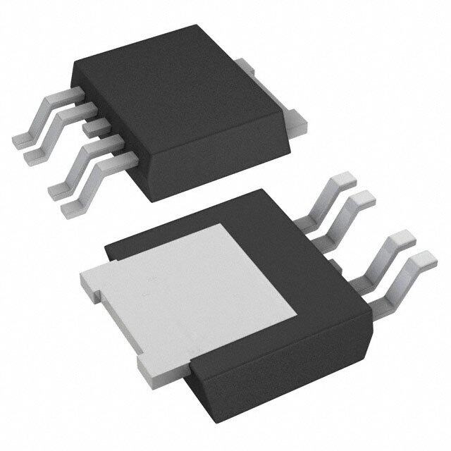
| 产品图片 |
|
| rohs | 符合RoHS无铅 / 符合限制有害物质指令(RoHS)规范要求 |
| 产品系列 | 电源管理 IC,门驱动器,STMicroelectronics VND14NV04TR-EOMNIFET II™, VIPower™ |
| 数据手册 | |
| 产品型号 | VND14NV04TR-E |
| 上升时间 | 350 ns |
| 下降时间 | 150 ns |
| 产品 | MOSFET Gate Drivers |
| 产品培训模块 | http://www.digikey.cn/PTM/IndividualPTM.page?site=cn&lang=zhs&ptm=26261 |
| 产品种类 | 门驱动器 |
| 供应商器件封装 | D-Pak |
| 其它名称 | 497-11687-2 |
| 其它有关文件 | http://www.st.com/web/catalog/sense_power/FM1965/CL1969/SC1038/PF65638?referrer=70071840 |
| 功率耗散 | 74 W |
| 包装 | 带卷 (TR) |
| 商标 | STMicroelectronics |
| 安装类型 | 表面贴装 |
| 安装风格 | SMD/SMT |
| 导通电阻 | 35 毫欧 |
| 封装 | Reel |
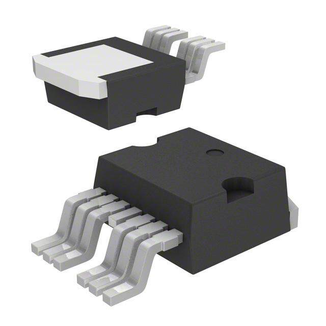
| 封装/外壳 | TO-252-3,DPak(2 引线+接片),SC-63 |
| 封装/箱体 | TO-252 |
| 工作温度 | -40°C ~ 150°C |
| 工厂包装数量 | 2500 |
| 最大关闭延迟时间 | 1350 ns |
| 最大功率耗散 | 74 W |
| 最大工作温度 | + 150 C |
| 最大开启延迟时间 | 250 ns |
| 最小工作温度 | - 40 C |
| 标准包装 | 2,500 |
| 激励器数量 | 1 Driver |
| 电压-电源 | - |
| 电流-峰值输出 | 18A |
| 电流-输出/通道 | 12A |
| 电源电流 | 20 mA |
| 类型 | Non-Inverting |
| 系列 | VND14NV04 |
| 输入类型 | 非反相 |
| 输出数 | 1 |
| 输出端数量 | 1 |
| 配置 | Single |


- 商务部:美国ITC正式对集成电路等产品启动337调查
- 曝三星4nm工艺存在良率问题 高通将骁龙8 Gen1或转产台积电
- 太阳诱电将投资9.5亿元在常州建新厂生产MLCC 预计2023年完工
- 英特尔发布欧洲新工厂建设计划 深化IDM 2.0 战略
- 台积电先进制程称霸业界 有大客户加持明年业绩稳了
- 达到5530亿美元!SIA预计今年全球半导体销售额将创下新高
- 英特尔拟将自动驾驶子公司Mobileye上市 估值或超500亿美元
- 三星加码芯片和SET,合并消费电子和移动部门,撤换高东真等 CEO
- 三星电子宣布重大人事变动 还合并消费电子和移动部门
- 海关总署:前11个月进口集成电路产品价值2.52万亿元 增长14.8%

_renders/CS4265-CNZR.jpg)


PDF Datasheet 数据手册内容提取
VNB14NV04, VND14NV04 VND14NV04-1, VNS14NV04 "OMNIFET II" fully autoprotected Power MOSFET Features TYPE R I V 3 3 DS(on) lim clamp 1 12 TO-252 (DPAK) TO-251 (IPAK) VNB14NV04 VND14NV04 35mΩ 12A 40V VND14NV04-1 VNS14NV04 3 1 ■ Linear current limitation SO-8 D2PAK ■ Thermal shutdown ■ Short circuit protection Description ■ Integrated clamp The VNB14NV04, VND14NV04, VND14NV04-1 and ■ Low current drawn from input pin VNS14NV04 are monolithic devices made using ■ Diagnostic feedback through input pin STMicroelectronics VIPower™ M0 technology, intended for replacement of standard power ■ ESD protection MOSFETS in DC to 50KHz applications. Built-in ■ Direct access to the gate of the Power thermal shutdown, linear current limitation and MOSFET (analog driving) overvoltage clamp protect the chip in harsh ■ Compatible with standard Power MOSFET environments. Fault feedback can be detected by monitoring the voltage at the input pin. Table 1. Device summary Package Tube Tube (lead free) Tape and reel Tape and reel (lead free) D2PAK VNB14NV04 VNB14NV04-E VNB14NV0413TR VNB14NV04TR-E TO-252 (DPAK) VND14NV04 VND14NV04-E VND14NV0413TR VND14NV04TR-E TO-251 (IPAK) VND14NV04-1 VND14NV04-1-E - - SO-8 VNS14NV04 - - - September 2013 Doc ID 7393 Rev 9 1/31 www.st.com 1
Contents VNB14NV04, VND14NV04, VND14NV04-1, VNS14NV04 Contents 1 Block diagram . . . . . . . . . . . . . . . . . . . . . . . . . . . . . . . . . . . . . . . . . . . . . . 5 2 Electrical specification . . . . . . . . . . . . . . . . . . . . . . . . . . . . . . . . . . . . . . . 6 2.1 Absolute maximum rating . . . . . . . . . . . . . . . . . . . . . . . . . . . . . . . . . . . . . . 6 2.2 Thermal data . . . . . . . . . . . . . . . . . . . . . . . . . . . . . . . . . . . . . . . . . . . . . . . 7 2.3 Electrical characteristics . . . . . . . . . . . . . . . . . . . . . . . . . . . . . . . . . . . . . . . 7 3 Protection features . . . . . . . . . . . . . . . . . . . . . . . . . . . . . . . . . . . . . . . . . . 9 4 Package thermal data . . . . . . . . . . . . . . . . . . . . . . . . . . . . . . . . . . . . . . . 18 4.1 DPAK thermal data . . . . . . . . . . . . . . . . . . . . . . . . . . . . . . . . . . . . . . . . . . 18 4.2 SO-8 thermal data . . . . . . . . . . . . . . . . . . . . . . . . . . . . . . . . . . . . . . . . . . 20 4.3 D2PAK thermal data . . . . . . . . . . . . . . . . . . . . . . . . . . . . . . . . . . . . . . . . . 21 5 Package information . . . . . . . . . . . . . . . . . . . . . . . . . . . . . . . . . . . . . . . . 24 5.1 ECOPACK® . . . . . . . . . . . . . . . . . . . . . . . . . . . . . . . . . . . . . . . . . . . . . . . 24 5.2 TO-251 (IPAK) mechanical data . . . . . . . . . . . . . . . . . . . . . . . . . . . . . . . . 24 5.3 D2PAK mechanical data . . . . . . . . . . . . . . . . . . . . . . . . . . . . . . . . . . . . . . 25 5.4 TO-252 (DPAK) mechanical data . . . . . . . . . . . . . . . . . . . . . . . . . . . . . . . 27 5.5 SO-8 mechanical data . . . . . . . . . . . . . . . . . . . . . . . . . . . . . . . . . . . . . . . 28 6 Revision history . . . . . . . . . . . . . . . . . . . . . . . . . . . . . . . . . . . . . . . . . . . 30 2/31 Doc ID 7393 Rev 9
VNB14NV04, VND14NV04, VND14NV04-1, VNS14NV04 List of tables List of tables Table 1. Device summary. . . . . . . . . . . . . . . . . . . . . . . . . . . . . . . . . . . . . . . . . . . . . . . . . . . . . . . . . . 1 Table 2. Absolute maximum rating. . . . . . . . . . . . . . . . . . . . . . . . . . . . . . . . . . . . . . . . . . . . . . . . . . . 6 Table 3. Thermal data. . . . . . . . . . . . . . . . . . . . . . . . . . . . . . . . . . . . . . . . . . . . . . . . . . . . . . . . . . . . . 7 Table 4. Electrical characteristics. . . . . . . . . . . . . . . . . . . . . . . . . . . . . . . . . . . . . . . . . . . . . . . . . . . . 7 Table 5. DPAK thermal parameter . . . . . . . . . . . . . . . . . . . . . . . . . . . . . . . . . . . . . . . . . . . . . . . . . . 19 Table 6. D2PAK thermal parameter . . . . . . . . . . . . . . . . . . . . . . . . . . . . . . . . . . . . . . . . . . . . . . . . . 22 Table 7. TO-251 (IPAK) mechanical data. . . . . . . . . . . . . . . . . . . . . . . . . . . . . . . . . . . . . . . . . . . . . 24 Table 8. D2PAK mechanical data. . . . . . . . . . . . . . . . . . . . . . . . . . . . . . . . . . . . . . . . . . . . . . . . . . . 26 Table 9. TO-252 (DPAK) mechanical data. . . . . . . . . . . . . . . . . . . . . . . . . . . . . . . . . . . . . . . . . . . . 27 Table 10. SO-8 mechanical data . . . . . . . . . . . . . . . . . . . . . . . . . . . . . . . . . . . . . . . . . . . . . . . . . . . . 28 Table 11. Document revision history . . . . . . . . . . . . . . . . . . . . . . . . . . . . . . . . . . . . . . . . . . . . . . . . . 30 Doc ID 7393 Rev 9 3/31
List of figures VNB14NV04, VND14NV04, VND14NV04-1, VNS14NV04 List of figures Figure 1. Block diagram. . . . . . . . . . . . . . . . . . . . . . . . . . . . . . . . . . . . . . . . . . . . . . . . . . . . . . . . . . . . 5 Figure 2. Current and voltage conventions . . . . . . . . . . . . . . . . . . . . . . . . . . . . . . . . . . . . . . . . . . . . . 6 Figure 3. Switching time test circuit for resistive load . . . . . . . . . . . . . . . . . . . . . . . . . . . . . . . . . . . . 10 Figure 4. Test circuit for diode recovery times. . . . . . . . . . . . . . . . . . . . . . . . . . . . . . . . . . . . . . . . . . 10 Figure 5. Unclamped inductive load test circuits . . . . . . . . . . . . . . . . . . . . . . . . . . . . . . . . . . . . . . . . 11 Figure 6. Unclamped inductive waveforms . . . . . . . . . . . . . . . . . . . . . . . . . . . . . . . . . . . . . . . . . . . . 11 Figure 7. Input charge test circuit. . . . . . . . . . . . . . . . . . . . . . . . . . . . . . . . . . . . . . . . . . . . . . . . . . . . 11 Figure 8. Source-drain diode forward characteristics . . . . . . . . . . . . . . . . . . . . . . . . . . . . . . . . . . . . 12 Figure 9. Static drain source on resistance . . . . . . . . . . . . . . . . . . . . . . . . . . . . . . . . . . . . . . . . . . . . 12 Figure 10. Derating curve . . . . . . . . . . . . . . . . . . . . . . . . . . . . . . . . . . . . . . . . . . . . . . . . . . . . . . . . . . 12 Figure 11. Static drain-source on resistance vs. input voltage (part 1/2). . . . . . . . . . . . . . . . . . . . . . . 12 Figure 12. Static drain-source on resistance vs. input voltage (part 2/2). . . . . . . . . . . . . . . . . . . . . . . 12 Figure 13. Transconductance . . . . . . . . . . . . . . . . . . . . . . . . . . . . . . . . . . . . . . . . . . . . . . . . . . . . . . . 12 Figure 14. Static drain-source on resistance vs. id . . . . . . . . . . . . . . . . . . . . . . . . . . . . . . . . . . . . . . . 13 Figure 15. Transfer characteristics . . . . . . . . . . . . . . . . . . . . . . . . . . . . . . . . . . . . . . . . . . . . . . . . . . . 13 Figure 16. Turn-on current slope (part 1/2) . . . . . . . . . . . . . . . . . . . . . . . . . . . . . . . . . . . . . . . . . . . . . 13 Figure 17. Turn-on current slope (part 2/2) . . . . . . . . . . . . . . . . . . . . . . . . . . . . . . . . . . . . . . . . . . . . . 13 Figure 18. Input voltage vs. input charge. . . . . . . . . . . . . . . . . . . . . . . . . . . . . . . . . . . . . . . . . . . . . . . 13 Figure 19. Turn-off drain source voltage slope (part 1/2). . . . . . . . . . . . . . . . . . . . . . . . . . . . . . . . . . . 13 Figure 20. Turn-off drain source voltage slope (part 2/2). . . . . . . . . . . . . . . . . . . . . . . . . . . . . . . . . . . 14 Figure 21. Capacitance variations. . . . . . . . . . . . . . . . . . . . . . . . . . . . . . . . . . . . . . . . . . . . . . . . . . . . 14 Figure 22. Switching time resistive load (part 1/2). . . . . . . . . . . . . . . . . . . . . . . . . . . . . . . . . . . . . . . . 14 Figure 23. Switching time resistive load (part 2/2). . . . . . . . . . . . . . . . . . . . . . . . . . . . . . . . . . . . . . . . 14 Figure 24. Output characteristics. . . . . . . . . . . . . . . . . . . . . . . . . . . . . . . . . . . . . . . . . . . . . . . . . . . . . 14 Figure 25. Normalized on resistance vs. temperature. . . . . . . . . . . . . . . . . . . . . . . . . . . . . . . . . . . . . 14 Figure 26. Normalized input threshold voltage vs. temperature . . . . . . . . . . . . . . . . . . . . . . . . . . . . . 15 Figure 27. Current limit vs. junction temperatures. . . . . . . . . . . . . . . . . . . . . . . . . . . . . . . . . . . . . . . . 15 Figure 28. Step response current limit. . . . . . . . . . . . . . . . . . . . . . . . . . . . . . . . . . . . . . . . . . . . . . . . . 15 Figure 29. DPAK maximum turn-off current versus load inductance. . . . . . . . . . . . . . . . . . . . . . . . . . 16 Figure 30. DPAK demagnetization. . . . . . . . . . . . . . . . . . . . . . . . . . . . . . . . . . . . . . . . . . . . . . . . . . . . 16 Figure 31. D2PAK maximum turn-off current versus load inductance . . . . . . . . . . . . . . . . . . . . . . . . . 17 Figure 32. D2PAK demagnetization. . . . . . . . . . . . . . . . . . . . . . . . . . . . . . . . . . . . . . . . . . . . . . . . . . . 17 Figure 33. DPAK PC board(1) . . . . . . . . . . . . . . . . . . . . . . . . . . . . . . . . . . . . . . . . . . . . . . . . . . . . . . . 18 Figure 34. DPAK R vs PCB copper area in open box free air condition. . . . . . . . . . . . . . . . . . . 18 thj-amb Figure 35. DPAK thermal impedance junction ambient single pulse. . . . . . . . . . . . . . . . . . . . . . . . . . 19 Figure 36. Thermal fitting model of an OMNIFET II in DPAK. . . . . . . . . . . . . . . . . . . . . . . . . . . . . . . . 19 Figure 37. SO-8 PC board(1) . . . . . . . . . . . . . . . . . . . . . . . . . . . . . . . . . . . . . . . . . . . . . . . . . . . . . . . . 20 Figure 38. SO-8 R vs PCB copper area in open box free air condition . . . . . . . . . . . . . . . . . . . 20 thj-amb Figure 39. D2PAK PC board(1). . . . . . . . . . . . . . . . . . . . . . . . . . . . . . . . . . . . . . . . . . . . . . . . . . . . . . . 21 Figure 40. D2PAK R vs PCB copper area in open box free air condition. . . . . . . . . . . . . . . . . . 21 thj-amb Figure 41. D2PAK thermal impedance junction ambient single pulse . . . . . . . . . . . . . . . . . . . . . . . . . 22 Figure 42. Thermal fitting model of an OMNIFET II in D2PAK. . . . . . . . . . . . . . . . . . . . . . . . . . . . . . . 22 Figure 43. TO-251 (IPAK) package dimension . . . . . . . . . . . . . . . . . . . . . . . . . . . . . . . . . . . . . . . . . . 24 Figure 44. D2PAK package dimension . . . . . . . . . . . . . . . . . . . . . . . . . . . . . . . . . . . . . . . . . . . . . . . . 25 Figure 45. TO-252 (DPAK) package dimension . . . . . . . . . . . . . . . . . . . . . . . . . . . . . . . . . . . . . . . . . 27 Figure 46. SO-8 package dimension. . . . . . . . . . . . . . . . . . . . . . . . . . . . . . . . . . . . . . . . . . . . . . . . . . 28 4/31 Doc ID 7393 Rev 9
VNB14NV04, VND14NV04, VND14NV04-1, VNS14NV04 Block diagram 1 Block diagram Figure 1. Block diagram Doc ID 7393 Rev 9 5/31
Electrical specification VNB14NV04, VND14NV04, VND14NV04-1, VNS14NV04 2 Electrical specification Figure 2. Current and voltage conventions 2.1 Absolute maximum rating Table 2. A bsolute maximum rating Value Symbol Parameter Unit SO-8 DPAK IPAK D2PAK V Drain-source voltage (V =0V) Internally clamped V DS IN V Input voltage Internally clamped V IN I Input current +/-20 mA IN R Minimum input series impedance 10 Ω IN MIN I Drain current Internally limited A D I Reverse DC output current -15 A R V Electrostatic discharge (R=1.5KΩ, C=100pF) 4000 V ESD1 Electrostatic discharge on output pin only V 16500 V ESD2 (R=330Ω, C=150pF) P Total dissipation at T=25°C 4.6 74 74 74 W tot c Maximum switching energy (L=0.4mH; R =0Ω; E L 93 93 mJ MAX V =13.5V; T =150°C; I =18A) bat jstart L T Operating junction temperature Internally limited °C j T Case operating temperature Internally limited °C c T Storage temperature -55 to 150 °C stg 6/31 Doc ID 7393 Rev 9
VNB14NV04, VND14NV04, VND14NV04-1, VNS14NV04 Electrical specification 2.2 Thermal data Table 3. T hermal data Value Symbol Parameter Unit SO-8 DPAK IPAK D2PAK Rthj-case Thermal resistance junction-case max 1.7 1.7 1.7 °C/W Rthj-lead Thermal resistance junction-lead max 27 °C/W Rthj-amb Thermal resistance junction-ambient max 90(1) 65(1) 102 52(1) °C/W 1. When mounted on a standard single-sided FR4 board with 0.5cm2 of Cu (at least 35µm thick) connected to all DRAIN pins. Horizontal mounting and no artificial air flow. 2.3 Electrical characteristics -40 < Tj < 150°C unless otherwise specified. Table 4. E lectrical characteristics Symbol Parameter Test Conditions Min Typ Max Unit Off VCLAMP Drain-source clamp voltage VIN=0V; ID=7A 40 45 55 V Drain-source clamp threshold V V =0V; I =2mA 36 V CLTH voltage IN D V Input threshold voltage V =V ; I =1mA 0.5 2.5 V INTH DS IN D IISS Supply current from input pin VDS=0V; VIN=5V 100 150 µA I =1mA 6 6.8 8 VINCL Input-source clamp voltage IIN=-1mA -1.0 -0.3 V IN Zero input voltage drain current V =13V; V =0V; T=25°C 30 IDSS (VIN=0V) VDDSS=25V; VIINN=0V j 75 µA On V = 5V I = 7A T = 25°C 35 R Static drain-source on resistance in D j mΩ DS(on) V = 5V I = 7A 70 in D Dynamic (Tj=25°C, unless otherwise specified) g (1) Forward transconductance V = 13V I = 7A 18 S fs DD D C Output capacitance V = 13V f = 1MHz V = 0V 400 pF oss DS IN Switching t Turn-on delay time 80 250 ns d(on) V = 15V I = 7A t Rise time DD D 350 1000 ns r V = 5V R = R =10Ω gen gen IN MIN t Turn-off delay time 450 1350 ns d(off) (see Figure3) t Fall time 150 500 ns f Doc ID 7393 Rev 9 7/31
Electrical specification VNB14NV04, VND14NV04, VND14NV04-1, VNS14NV04 Table 4. Electrical characteristics (continued) Symbol Parameter Test Conditions Min Typ Max Unit t Turn-on delay time 1.5 4.5 µs d(on) V = 15V I = 7A t Rise time DD d 9.7 30.0 µs r V = 5V R = 2.2KΩ gen gen t Turn-off delay time 25.0 µs d(off) (see Figure3) t Fall time 10.2 30.0 µs f V = 15V I = 7A (di/dt) Turn-on current slope DD D 16 A/µs on V = 5V R = R =10Ω gen gen IN MIN V = 12V I = 7A V = 5V; Q Total input charge DD D in 36.8 nC i I = 2.13mA (see Figure7) gen Source drain diode V (1) Forward on voltage I = 7A V = 0V 0.8 V SD SD in t Reverse recovery time 300 ns rr I = 7A; di/dt= 40A/µs SD Q Reverse recovery charge V = 30V L = 200µH 0.8 µC rr DD (see test circuit, Figure4) I Reverse recovery current 5 A RRM Protection I Drain current limit V = 5V; V = 13V 12 18 24 A lim IN DS tdlim Step response current limit VIN = 5V; VDS = 13V 45 µs T Over temperature shutdown 150 175 200 °C jsh T Over temperature reset 135 °C jrs Igf Fault sink current VIN = 5V; VDS = 13V; Tj = Tjsh 10 15 20 mA starting T = 25°C; V = 24V j DD V = 5V; R = R = 10Ω; E Single pulse avalanche energy IN gen IN MIN 400 mJ as L = 24mH (see Figure5 and Figure6) 1. Pulsed: Pulse duration = 300µs, duty cycle 1.5% 8/31 Doc ID 7393 Rev 9
VNB14NV04, VND14NV04, VND14NV04-1, VNS14NV04 Protection features 3 Protection features During normal operation, the input pin is electrically connected to the gate of the internal power MOSFET through a low impedance path. The device then behaves like a standard power MOSFET and can be used as a switch from DC up to 50KHz. The only difference from the user’s standpoint is that a small DC current I (typ. 100µA) flows into the input pin in order to supply the internal circuitry. ISS The device integrates: ● Overvoltage clamp protection: internally set at 45V, along with the rugged avalanche characteristics of the Power MOSFET stage give this device unrivalled ruggedness and energy handling capability. This feature is mainly important when driving inductive loads. ● Linear current limiter circuit: limits the drain current I to I whatever the input pin D lim voltages. When the current limiter is active, the device operates in the linear region, so power dissipation may exceed the capability of the heatsink. Both case and junction temperatures increase, and if this phase lasts long enough, junction temperature may reach the over temperature threshold T . jsh ● Over temperature and short circuit protection: these are based on sensing the chip temperature and are not dependent on the input voltage. The location of the sensing element on the chip in the power stage area ensures fast, accurate detection of the junction temperature. Over temperature cutout occurs in the range 150 to 190°C, a typical value being 170°C. The device is automatically restarted when the chip temperature falls of about 15°C below shutdown temperature. ● Status feedback: in the case of an over temperature fault condition (T > T ), the j jsh device tries to sink a diagnostic current Igf through the input pin in order to indicate fault condition. If driven from a low impedance source, this current may be used in order to warn the control circuit of a device shutdown. If the drive impedance is high enough so that the input pin driver is not able to supply the current I , the input pin will fall to 0V. gf This will not however affect the device operation: no requirement is put on the current capability of the input pin driver except to be able to supply the normal operation drive current I . ISS Additional features of this device are ESD protection according to the Human Body model and the ability to be driven from a TTL Logic circuit. Doc ID 7393 Rev 9 9/31
Protection features VNB14NV04, VND14NV04, VND14NV04-1, VNS14NV04 Figure 3. Switching time test circuit for resistive load Figure 4. Test circuit for diode recovery times 10/31 Doc ID 7393 Rev 9
VNB14NV04, VND14NV04, VND14NV04-1, VNS14NV04 Protection features Figure 5. Unclamped inductive load test Figure 6. Unclamped inductive waveforms circuits Figure 7. Input charge test circuit Doc ID 7393 Rev 9 11/31
Protection features VNB14NV04, VND14NV04, VND14NV04-1, VNS14NV04 Figure 8. Source-drain diode forward Figure 9. Static drain source on resistance characteristics Figure 10. Derating curve Figure 11. Static drain-source on resistance vs. input voltage (part 1/2) Figure 12. Static drain-source on resistance Figure 13. Transconductance vs. input voltage (part 2/2) 12/31 Doc ID 7393 Rev 9
VNB14NV04, VND14NV04, VND14NV04-1, VNS14NV04 Protection features Figure 14. Static drain-source on resistance Figure 15. Transfer characteristics vs. id Figure 16. Turn-on current slope (part 1/2) Figure 17. Turn-on current slope (part 2/2) Figure 18. Input voltage vs. input charge Figure 19. Turn-off drain source voltage slope (part 1/2) Doc ID 7393 Rev 9 13/31
Protection features VNB14NV04, VND14NV04, VND14NV04-1, VNS14NV04 Figure 20. Turn-off drain source voltage slope Figure 21. Capacitance variations (part 2/2) Figure 22. Switching time resistive load (part Figure 23. Switching time resistive load (part 1/2) 2/2) Figure 24. Output characteristics Figure 25. Normalized on resistance vs. temperature 14/31 Doc ID 7393 Rev 9
VNB14NV04, VND14NV04, VND14NV04-1, VNS14NV04 Protection features Figure 26. Normalized input threshold voltage Figure 27. Current limit vs. junction vs. temperature temperatures Figure 28. Step response current limit Doc ID 7393 Rev 9 15/31
Protection features VNB14NV04, VND14NV04, VND14NV04-1, VNS14NV04 Figure 29. DPAK maximum turn-off current versus load inductance Legend: A= Single pulse at T =150ºC Jstart B= Repetitive pulse at T =100ºC Jstart C= Repetitive pulse at T =125ºC Jstart Conditions: V =13.5V CC Values are generated with R =0Ω L In case of repetitive pulses, T (at beginning of each demagnetization) of every pulse jstart must not exceed the temperature specified above for curves B and C. Figure 30. DPAK demagnetization 16/31 Doc ID 7393 Rev 9
VNB14NV04, VND14NV04, VND14NV04-1, VNS14NV04 Protection features Figure 31. D2PAK maximum turn-off current versus load inductance Legend: A= Single pulse at T =150ºC Jstart B= Repetitive pulse at T =100ºC Jstart C= Repetitive pulse at T =125ºC Jstart Conditions: V =13.5V CC Values are generated with R =0Ω L In case of repetitive pulses, T (at beginning of each demagnetization) of every pulse jstart must not exceed the temperature specified above for curves B and C. Figure 32. D2PAK demagnetization Doc ID 7393 Rev 9 17/31
Package thermal data VNB14NV04, VND14NV04, VND14NV04-1, VNS14NV04 4 Package thermal data 4.1 DPAK thermal data Figure 33. DPAK PC board(1) 1. Layout condition of R and Z measurements (PCB FR4 area= 60mm x 60mm, PCB thickness=2mm, Cu thickness=35µm, thCoppert hareas: from minimum pad lay-out to 8cm2). Figure 34. DPAK R vs PCB copper area in open box free air condition thj-amb 18/31 Doc ID 7393 Rev 9
VNB14NV04, VND14NV04, VND14NV04-1, VNS14NV04 Package thermal data Figure 35. DPAK thermal impedance junction ambient single pulse Figure 36. Thermal fitting model of an OMNIFET II in DPAK Pulse calculation formula Z = R ⋅δ+Z (1–δ) THδ TH THtp where δ = t ⁄T p T able 5. DPAK thermal parameter Area/island(cm2) Footprint 6 R1 (°C/W) 0.1 R2 (°C/W) 0.35 R3 ( °C/W) 1.20 R4 (°C/W) 2 R5 (°C/W) 15 R6 (°C/W) 61 24 C1 (W.s/°C) 0.0006 C2 (W.s/°C) 0.0021 C3 (W.s/°C) 0.05 Doc ID 7393 Rev 9 19/31
Package thermal data VNB14NV04, VND14NV04, VND14NV04-1, VNS14NV04 Table 5. DPAK thermal parameter (continued) Area/island(cm2) Footprint 6 C4 (W.s/°C) 0.3 C5 (W.s/°C) 0.45 C6 (W.s/°C) 0.8 5 4.2 SO-8 thermal data Figure 37. SO-8 PC board(1) 1. Layout condition of R and Z measurements (PCB FR4 area= 58mm x 58mm, PCB thickness=2mm, Cu thickness=35µm, thCoppert hareas: 0.14cm2, 0.6cm2, 1.6cm2). Figure 38. SO-8 R vs PCB copper area in open box free air condition thj-amb 20/31 Doc ID 7393 Rev 9
VNB14NV04, VND14NV04, VND14NV04-1, VNS14NV04 Package thermal data 2 4.3 D PAK thermal data Figure 39. D2PAK PC board(1) 1. Layout condition of R and Z measurements (PCB FR4 area= 60mm x 60mm, PCB thickness=2mm, Cu thickness=35µm, thCoppert hareas: from minimum pad lay-out to 8cm2). Figure 40. D2PAK R vs PCB copper area in open box free air condition thj-amb Doc ID 7393 Rev 9 21/31
Package thermal data VNB14NV04, VND14NV04, VND14NV04-1, VNS14NV04 Figure 41. D2PAK thermal impedance junction ambient single pulse Figure 42. Thermal fitting model of an OMNIFET II in D2PAK Pulse calculation formula Z = R ⋅δ+Z (1–δ) THδ TH THtp where δ = t ⁄T p T able 6. D2PAK thermal parameter Area/island(cm2) Footprint 6 R1 (°C/W) 0.1 R2 (°C/W) 0.35 R3 ( °C/W) 0.3 R4 (°C/W) 4 R5 (°C/W) 9 R6 (°C/W) 37 22 C1 (W.s/°C) 0.0006 C2 (W.s/°C) 2.10E-03 22/31 Doc ID 7393 Rev 9
VNB14NV04, VND14NV04, VND14NV04-1, VNS14NV04 Package thermal data Table 6. D2PAK thermal parameter (continued) Area/island(cm2) Footprint 6 C3 (W.s/°C) 8.00E-02 C4 (W.s/°C) 0.45 C5 (W.s/°C) 2 C6 (W.s/°C) 3 5 Doc ID 7393 Rev 9 23/31
Package information VNB14NV04, VND14NV04, VND14NV04-1, VNS14NV04 5 Package information ® 5.1 ECOPACK In order to meet environmental requirements, ST offers these devices in different grades of ECOPACK® packages, depending on their level of environmental compliance. ECOPACK® specifications, grade definitions and product status are available at: www.st.com. ECOPACK® is an ST trademark. 5.2 TO-251 (IPAK) mechanical data Figure 43. TO-251 (IPAK) package dimension T able 7. TO-251 (IPAK) mechanical data Millimeters Dim. Min. Typ. Max. A 2.2 2.4 A1 0.9 1.1 A3 0.7 1.3 B 0.64 0.9 B2 5.2 5.4 24/31 Doc ID 7393 Rev 9
VNB14NV04, VND14NV04, VND14NV04-1, VNS14NV04 Package information Table 7. TO-251 (IPAK) mechanical data (continued) Millimeters Dim. Min. Typ. Max. B3 0.85 B5 0.3 B6 0.95 C 0.45 0.6 C2 0.48 0.6 D 6 6.2 E 6.4 6.6 G 4.4 4.6 H 15.9 16.3 L 9 9.4 L1 0.8 1.2 L2 0.8 1 2 5.3 D PAK mechanical data Figure 44. D2PAK package dimension Doc ID 7393 Rev 9 25/31
Package information VNB14NV04, VND14NV04, VND14NV04-1, VNS14NV04 T able 8. D2PAK mechanical data Millimeters Dim. Min. Typ. Max. A 4.4 4.6 A1 2.49 2.69 A2 0.03 0.23 B 0.7 0.93 B2 1.14 1.7 C 0.45 0.6 C2 1.23 1.36 D 8.95 9.35 D1 8 E 10 10.4 E1 8.5 G 4.88 5.28 L 15 15.85 L2 1.27 1.4 L3 1.4 1.75 M 2.4 3.2 R 0.4 V2 0° 8° 26/31 Doc ID 7393 Rev 9
VNB14NV04, VND14NV04, VND14NV04-1, VNS14NV04 Package information 5.4 TO-252 (DPAK) mechanical data Figure 45. TO-252 (DPAK) package dimension T able 9. TO-252 (DPAK) mechanical data Millimeters Dim. Min. Typ. Max. A 2.20 2.40 A1 0.90 1.10 A2 0.03 0.23 B 0.64 0.90 B2 5.20 5.40 C 0.45 0.6 C2 0.48 0.6 D 6 6.20 D1 5.1 E 6.4 6.6 E1 4.7 e 2.28 G 4.4 4.6 H 9.35 10.1 L2 0.8 Doc ID 7393 Rev 9 27/31
Package information VNB14NV04, VND14NV04, VND14NV04-1, VNS14NV04 Table 9. TO-252 (DPAK) mechanical data (continued) Millimeters Dim. Min. Typ. Max. L4 0.6 1 R 0.2 V2 0° 8° Package weight Gr. 0.29 5.5 SO-8 mechanical data Figure 46. SO-8 package dimension T able 10. SO-8 mechanical data Millimeters Dim. Min. Typ. Max. A 1.75 2.40 a1 0.25 0.1 a2 1.65 b 0.85 0.35 b1 0.25 0.19 28/31 Doc ID 7393 Rev 9
VNB14NV04, VND14NV04, VND14NV04-1, VNS14NV04 Package information Table 10. SO-8 mechanical data (continued) Millimeters Dim. Min. Typ. Max. C 0.5 0.25 c1 45 D 5 4.8 E 6.2 5.8 e 1.27 e3 3.81 F 4 3.8 L 1.27 0.4 M 0.6 F 8 Doc ID 7393 Rev 9 29/31
Revision history VNB14NV04, VND14NV04, VND14NV04-1, VNS14NV04 6 Revision history T able 11. Document revision history Date Revision Changes 21-Jun-2004 6 Initial release. Document reformatted. 03-Apr-2009 7 Added Table1: Device summary on page1. Updated Section5: Package information on page24 Added part number VNS14NV04. Added SO-8 package: – Updated Table1: Device summary 06-Apr-2010 8 – Updated Table2: Absolute maximum rating – Updated Table3: Thermal data – Updated Chapter4: Package thermal data – Updated Chapter5: Package information 20-Sep-2013 9 Updated Disclaimer. 30/31 Doc ID 7393 Rev 9
VNB14NV04, VND14NV04, VND14NV04-1, VNS14NV04 Please Read Carefully: Information in this document is provided solely in connection with ST products. STMicroelectronics NV and its subsidiaries (“ST”) reserve the right to make changes, corrections, modifications or improvements, to this document, and the products and services described herein at any time, without notice. All ST products are sold pursuant to ST’s terms and conditions of sale. Purchasers are solely responsible for the choice, selection and use of the ST products and services described herein, and ST assumes no liability whatsoever relating to the choice, selection or use of the ST products and services described herein. No license, express or implied, by estoppel or otherwise, to any intellectual property rights is granted under this document. If any part of this document refers to any third party products or services it shall not be deemed a license grant by ST for the use of such third party products or services, or any intellectual property contained therein or considered as a warranty covering the use in any manner whatsoever of such third party products or services or any intellectual property contained therein. UNLESS OTHERWISE SET FORTH IN ST’S TERMS AND CONDITIONS OF SALE ST DISCLAIMS ANY EXPRESS OR IMPLIED WARRANTY WITH RESPECT TO THE USE AND/OR SALE OF ST PRODUCTS INCLUDING WITHOUT LIMITATION IMPLIED WARRANTIES OF MERCHANTABILITY, FITNESS FOR A PARTICULAR PURPOSE (AND THEIR EQUIVALENTS UNDER THE LAWS OF ANY JURISDICTION), OR INFRINGEMENT OF ANY PATENT, COPYRIGHT OR OTHER INTELLECTUAL PROPERTY RIGHT. ST PRODUCTS ARE NOT DESIGNED OR AUTHORIZED FOR USE IN: (A) SAFETY CRITICAL APPLICATIONS SUCH AS LIFE SUPPORTING, ACTIVE IMPLANTED DEVICES OR SYSTEMS WITH PRODUCT FUNCTIONAL SAFETY REQUIREMENTS; (B) AERONAUTIC APPLICATIONS; (C) AUTOMOTIVE APPLICATIONS OR ENVIRONMENTS, AND/OR (D) AEROSPACE APPLICATIONS OR ENVIRONMENTS. WHERE ST PRODUCTS ARE NOT DESIGNED FOR SUCH USE, THE PURCHASER SHALL USE PRODUCTS AT PURCHASER’S SOLE RISK, EVEN IF ST HAS BEEN INFORMED IN WRITING OF SUCH USAGE, UNLESS A PRODUCT IS EXPRESSLY DESIGNATED BY ST AS BEING INTENDED FOR “AUTOMOTIVE, AUTOMOTIVE SAFETY OR MEDICAL” INDUSTRY DOMAINS ACCORDING TO ST PRODUCT DESIGN SPECIFICATIONS. PRODUCTS FORMALLY ESCC, QML OR JAN QUALIFIED ARE DEEMED SUITABLE FOR USE IN AEROSPACE BY THE CORRESPONDING GOVERNMENTAL AGENCY. Resale of ST products with provisions different from the statements and/or technical features set forth in this document shall immediately void any warranty granted by ST for the ST product or service described herein and shall not create or extend in any manner whatsoever, any liability of ST. ST and the ST logo are trademarks or registered trademarks of ST in various countries. Information in this document supersedes and replaces all information previously supplied. The ST logo is a registered trademark of STMicroelectronics. All other names are the property of their respective owners. © 2013 STMicroelectronics - All rights reserved STMicroelectronics group of companies Australia - Belgium - Brazil - Canada - China - Czech Republic - Finland - France - Germany - Hong Kong - India - Israel - Italy - Japan - Malaysia - Malta - Morocco - Philippines - Singapore - Spain - Sweden - Switzerland - United Kingdom - United States of America www.st.com Doc ID 7393 Rev 9 31/31
Mouser Electronics Authorized Distributor Click to View Pricing, Inventory, Delivery & Lifecycle Information: S TMicroelectronics: VND14NV04 VND14NV04-1 VNB14NV04 VND14NV0413TR VNB14NV0413TR VNB14NV04-E VNB14NV04TR-E VND14NV04-1-E VND14NV04-E VND14NV04TR-E