ICGOO在线商城 > VNCLO-SHLD-1A
/MFG_VNCLO-SHLD.jpg)
 Datasheet下载
- 型号: VNCLO-SHLD-1A
- 制造商: FTDI
- 库位|库存: xxxx|xxxx
- 要求:
| 数量阶梯 | 香港交货 | 国内含税 |
| +xxxx | $xxxx | ¥xxxx |
查看当月历史价格
查看今年历史价格
VNCLO-SHLD-1A产品简介:
ICGOO电子元器件商城为您提供VNCLO-SHLD-1A由FTDI设计生产,在icgoo商城现货销售,并且可以通过原厂、代理商等渠道进行代购。 提供VNCLO-SHLD-1A价格参考以及FTDIVNCLO-SHLD-1A封装/规格参数等产品信息。 你可以下载VNCLO-SHLD-1A参考资料、Datasheet数据手册功能说明书, 资料中有VNCLO-SHLD-1A详细功能的应用电路图电压和使用方法及教程。
| 参数 | 数值 |
| 产品目录 | 编程器,开发系统嵌入式解决方案 |
| 描述 | MOD VINCo PIGGYBACK BOARD子卡和OEM板 Vinco Prototyping Shield Accessory |
| 产品分类 | |
| 品牌 | FTDI |
| 产品手册 | |
| 产品图片 |
|
| rohs | 符合RoHS无铅 / 符合限制有害物质指令(RoHS)规范要求 |
| 产品系列 | 嵌入式开发工具,嵌入式工具与配件,子卡和OEM板,FTDI VNCLO-SHLD-1AVinco |
| 数据手册 | |
| 产品型号 | VNCLO-SHLD-1A |
| PCN设计/规格 | |
| 产品 | Arduino Compatible Shields |
| 产品种类 | 子卡和OEM板 |
| 其它名称 | 768-1090 |
| 商标 | FTDI |
| 封装 | Bulk |
| 工作电源电压 | 5 V |
| 工具用于评估 | VNC2-64Q |
| 工厂包装数量 | 25 |
| 应用说明 | 点击此处下载产品Datasheet点击此处下载产品Datasheet点击此处下载产品Datasheet点击此处下载产品Datasheet |
| 接口类型 | USB |
| 数据总线宽度 | 16 bit |
| 标准包装 | 5 |
| 特色产品 | http://www.digikey.com/product-highlights/cn/zh/ftdi-vinco/1050 |
| 用于 | VNCLO-MB1A |
| 配件类型 | 扩展模块 |
| 配套使用产品/相关产品 | VNCLO-MB1A |
| 配用 | /product-detail/zh/VNCLO-MB1A/768-1088-ND/2498969 |


PDF Datasheet 数据手册内容提取
Future Technology Devices International Ltd. Vinco Development Module Datasheet The Vinco module is a Vinculum based development platform inspired by Arduino projects. Document Reference No.: FT_000327 Version 2.01 Issue Date: 2012-11-06 Future Technology Devices International Ltd (FTDI) Unit 1, 2 Seaward Place, Centurion Business Park, Glasgow, G41 1HH, United Kingdom Tel.: +44 (0) 141 429 2777 Fax: + 44 (0) 141 429 2758 E-Mail (Support): support1@ftdichip.com Web: www.ftdichip.com Use of FTDI devices in life support and/or safety applications is entirely at the user’s risk, and the user agrees to defend, indemnify and hold harmless FTDI from any and all damages, claims, suits or expense resulting from such use. Copyright © 2010 Future Technology Devices International Limited
Document Reference No.: FT_000327 Vinco Development Module Datasheet Version 2.01 Clearance No.: FTDI#173 1 Introduction Vinco is a development module based on the FTDI Vinculum II, VNC2 dual USB host/slave IC. Vinco is designed as a prototyping platform for VNC2 based designs and applications. The mechanical form of the module, and the concept of providing free software development library and tools, is inspired by the Arduino concept. Vinco is a superset of the Duemilanove / Uno with 2 extra rows of headers providing an extra 10 pins. The Vinco programming language utilises a subset of standard ANSII ‘C’ with FTDI supported, free of charge software development tools, libraries and reference designs for fast prototyping different modules including support for a variety of USB classes such as Mass Storage, Human Interface Devices (keyboards, mice), audio devices, video devices (webcam) and many more still under development. Vinco may also be used with many existing Arduino shields by porting the firmware to run on the VNC2 IC. The module uses a VNC2-64Q package to facilitate 38 GPIO options on 0.1” pitch header pins. A 10 bit A/D converter has also been added to offer connectivity to analogue inputs. This A/D converter can be read by the VNC2-64Q SPI host interface. For USB connectivity the module includes one USB type A connector for a USB host port and one mini- B connector for a USB slave port to provide access to the VNC2-64Q USB ports. An additional connector, to mate with the VII debugger/programmer module, (also available from FTDI) is provided to connect to the VNC2 IDE (Integrated Development Environment) for creating and debugging application code to run on the Vinco module. The debugger/programmer module also allows the Vinco module to be programmed. This can be done by taking a .ROM file of the application source code and flash into the VNC2-64Q through a USB connection via a PC. For further details on how to program the VNC2, please see applications Note Vinculum-II Debug Interface Description. A bare prototyping Vinco PCB (Vinco_Proto) which has the same PCB form factor as the Vinco is also available. This can be used to prototype most shield application, comes with a selection of components and mates directly to the Vinco connectors in a style similar to Arduino shields. Figure 1.1 – VINCO Copyright © 2012 Future Technology Devices International Limited 1
Document Reference No.: FT_000327 Vinco Development Module Datasheet Version 2.01 Clearance No.: FTDI#173 1.1 Key Features The Vinco incorporates the following features: Microcontroller: VNC2-64Q Operating voltage: 5V Input power supply: 9V Digital I/O: 30 Analogue I/O: 8 USB port: 2 – configurable for host or device operation FLASH memory: 256kbytes RAM: 16kbytes Variable clock speeds: 12/24/48MHz Superset of the Arduino Duemilanove / Uno development boards. FTDI Integrated Development Environment (IDE) including code editor, compiler, assembler and debugger, which is supplied free of charge, and supports ANSII C coding for easy portability and maintainability. Precompiled drivers for a variety of interfaces e.g. USB, UART, SPI. Precompiled driver support for a wide range of USB host classes including Mass Storage, Human Interface Devices (keyboards, mice), audio devices, video devices (webcam) with many more under development. Precompiled driver support for a wide range of USB device classes including FTDI peripheral ICs, Human Interface Devices (keyboards, mice) with many more under developed. Compatible with existing Arduino shields. A software configuration wizard is currentlty under development. 1.2 VNC2 IC VNC2 is the second of FTDI’s Vinculum family of Embedded dual USB host controller devices. VNC2 device provides USB Host interfacing capability for a variety of different USB device classes including support for BOMS (bulk only mass storage), Printer, HID (human interface devices). For mass storage devices such as USB Flash drives, VNC2 also transparently handles the FAT file structure. Communication with non USB devices such as a low cost microcontroller is accomplished via either UART, SPI or parallel FIFO interfaces. VNC2 provides a new cost effective solution for providing USB Host capability into products that previously did not have the hardware resources available. VNC2 has the capability to enable customers to develop custom firmware using the Vinculum II development software tool suite. The development tools support compiler, assembler, linker and debugger tools complete within an integrated development environment (IDE). The Vinculum-II family of devices are available in Pb-free (RoHS compliant) 32-lead LQFP, 32-lead QFN, 48-lead LQFP, 48-lead QFN, 64-Lead LQFP and 64-lead QFN packages For more information on the ICs refer to http://www.ftdichip.com/Products/ICs/VNC2.htm Copyright © 2012 Future Technology Devices International Limited 2
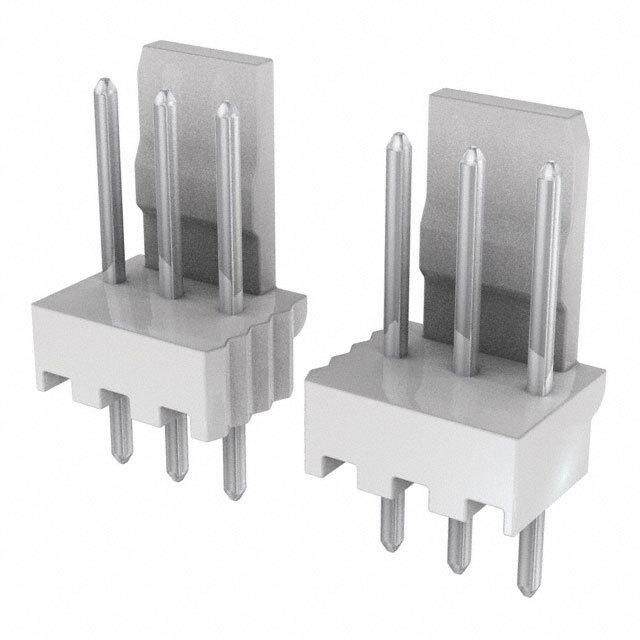
Document Reference No.: FT_000327 Vinco Development Module Datasheet Version 2.01 Clearance No.: FTDI#173 1.3 Part Numbers Part Number Description VNCLO-MB1A Vinco Motherboard VNCLO-PSU-US Vinco +9V/1A PSU ( Optional ) - USA VNCLO-PSU-EU Vinco +9V/1A PSU ( Optional ) - Europe VNCLO-PSU-UK Vinco +9V/1A PSU ( Optional ) - UK VNCLO-SHLD1A Vinco_Proto prototyping shield (Optional) VNC2 DEBUG MODULE VNC2 debugger/programmer module VNCLO-START1 Vinco and a debugger/programmer module VNCLO-START1 VNCLO-SHLD-1A * 2pc VNCLO-PREM1 VNCLO-PSU-XX (dependent regional requirement (UK/US/EU) A mini B cable USB "A" to Mini-"B" Cable, 1m USB A to mini-"B" Cable, 1m Table 1.1 – Vinco Part Numbers Copyright © 2012 Future Technology Devices International Limited 3
Document Reference No.: FT_000327 Vinco Development Module Datasheet Version 2.01 Clearance No.: FTDI#173 Table of Contents 1 Introduction .................................................................... 1 1.1 Key Features ............................................................................. 2 1.2 VNC2 IC .................................................................................... 2 1.3 Part Numbers ............................................................................ 3 2 Functionality ................................................................... 3 2.1 Power ....................................................................................... 3 2.2 Input/Output ............................................................................ 3 2.3 LEDs & PWREN# ....................................................................... 3 3 Pin Out and Signal Description ........................................ 4 3.1 Module Connector Descriptions ................................................. 4 3.2 Vinco Connectors : Pins and Signal Description ........................ 5 3.3 USB Slave Port : Pins and Signal Description ............................ 7 3.4 USB Host Port : Pins and Signal Description .............................. 7 3.5 Configuration Jumpers .............................................................. 8 4 Configurable Pin outs ...................................................... 9 4.1 UART Interface ......................................................................... 9 4.1.1 Signal Description – UART Interface ............................................................. 9 4.2 Serial Peripheral Interface (SPI) ............................................ 10 4.2.1 Signal Description - SPI Slave ................................................................... 10 4.2.2 Signal Description - SPI Master ................................................................. 10 4.3 Parallel FIFO Interface - Asynchronous Mode ......................... 11 4.3.1 Signal Description - Parallel FIFO Interface ................................................. 11 5 Debugger Interface ....................................................... 12 5.1 Signal Description - Debugger Interface ................................. 12 6 ADC Converter ............................................................... 13 7 Firmware ....................................................................... 14 7.1 Firmware Support ................................................................... 14 7.2 Available Firmware ................................................................. 14 7.3 Firmware Upgrades ................................................................. 14 7.4 Arduino Shield Compatible Firmware ...................................... 14 8 Mechanical Dimensions ................................................. 15 9 Schematic Diagram ....................................................... 16 Copyright © 2012 Future Technology Devices International Limited 1
Document Reference No.: FT_000327 Vinco Development Module Datasheet Version 2.01 Clearance No.: FTDI#173 10 Arduino Shields ............................................................. 17 11 Contact Information ...................................................... 18 Appendix A – References ................................................................. 19 Appendix B – List of Figures and Tables .......................................... 20 List of Figures ................................................................................. 20 List of Tables ................................................................................... 20 Appendix C – Revision History ......................................................... 21 Copyright © 2012 Future Technology Devices International Limited 2
Document Reference No.: FT_000327 Vinco Development Module Datasheet Version 2.01 Clearance No.: FTDI#173 2 Functionality 2.1 Power The Vinco requires +5V for the USB host ports to power USB devices from the module. This is further regulated to +3.3V for VNC2. A +9V/1A DC supply is also available which can be used as an AC-DC adapter (wall-wart). The +9V is regulated to +5V and +3V3 on the Vinco module. As an alternative to the AC-DC adapter the on board regulators can be taken out of circuit with jumpers to allow the +5V from a USB host port to power the module. Care should be taken with this approach as a USB host port can only provide a maximum of 500mA, which must power the Vinco and potentially any devices connected to the Vinco. The +5V and +3V3 supplies may also be accessed on the J1 header pins. VNC2 requires between 8 and 24mA depending on the clock speed at which the VNC2 core is running. 2.2 Input/Output Due to the flexibility of the VNC2 IC the actual definition of each pin is not fixed. The firmware developed for any application can use the VNC2 IO Mux to route a signal, e.g. UART TXD, to a range of IO pins. An IOMux utility built into the free tool chain development environment, IDE, allows the developer to define the IO from a GUI interface. The utility will then convert the users IO selection into C code to be included as part of the project firmware... There are 38 configurable IO pins available to the user, 8 of which are reserved for connecting to the onboard ADC device. The other 30 pins may be used for GPIO, UART, SPI or FIFO connectivity depending on the interface of the shield designed to connect to the Vinco module. There are 2 USB ports on the Vinco. The firmware will determine if the port is configured for USB host operation or USB device operation. 2.3 LEDs & PWREN# There are 3 LEDs and one power control signal, PWREN# on Vinco. LED1 is driven by the VNC2-64Q IC depending on which firmware is loaded. It may be used to indicate traffic on the USB slave port connected via CN3. LED1 is connected to the VNC2-64Q IC on pin 39. Configure this pin for a GPIO output in order to use this LED. LED2 is driven by the VNC2-64Q IC depending on which firmware is loaded. It may be used to indicate traffic on the USB host port connected via CN2.LED2 is connected to the VNC2-64Q IC on pin 40. Configure this pin for a GPIO output in order to use this LED. LED3 is driven by the 3V3 supply that also powers the VNC2-64Q IC. It will indicate when the Vinco module is powered. PWREN# is a signal that controls the power output to the USB Host connector, CN2. PWREN# is connected to the VNC2-64Q IC on pin 41. Configure this pin for a GPIO output in order to make power available at CN2 for USB peripherals. Copyright © 2012 Future Technology Devices International Limited 3
Document Reference No.: FT_000327 Vinco Development Module Datasheet Version 2.01 Clearance No.: FTDI#173 3 Pin Out and Signal Description 3.1 Module Connector Descriptions CN1 CN2 3 N C D2 D1 LED3 LE LE JP1 46 JJ SW2 JP2 1 U1 1 35 J1 JJ 1 U2 J2 1 1 J7 Figure 3.1 – Vinco Diagram A detailed description of each pin out is given in the next section. CONNECTOR FUNCTION CN1 Power input CN2 USB host port CN3 USB slave port J1 Interface to shield boards J2 Interface to shield boards J3 Interface to shield boards J4 Interface to shield boards J5 Interface to shield boards J6 Interface to shield boards J7 Debug port Table 3.1 – Vinco Connector Descriptions Copyright © 2012 Future Technology Devices International Limited 4
Document Reference No.: FT_000327 Vinco Development Module Datasheet Version 2.01 Clearance No.: FTDI#173 3.2 Vinco Connectors : Pins and Signal Description Pin No. Name Pin Name Type Description on PCB 9V module supply pin. This pin can be used to provide the 5.0V input to the Vinco when the V2DIP2-64 is not CN1 9V PWR PWR Input powered from the USB connector (VBUS) or the debugger interface. Also connected to DIL connector pins J1-1 and J3-6. CN2 USB USB2 USB host port Connects to VNC2-64Q USB port 2 CN3 USB USB1 USB slave port Connects to VNC2-64Q USB port 1 Analogue input to channel 6 of the ADC J1-1 AIN6 ADC6 Analogue Input or 5V safe bidirectional data/control bus bit 30 Analogue input to channel 7 of the ADC J1-2 AIN7 ADC7 Analogue Input or 5V safe bidirectional data/control bus bit 31 J1-3 RESET# RESET# Input Reset for the VNC2-64Q J1-4 VCC3V3 3V3 PWR Output 3V3 output for external circuitry J1-5 VCC5V 5V Power output 5V output for external circuitry J1-6 GND GND GND GND for PCB J1-7 GND GND GND GND for PCB J1-8 VCCIN VCCIN PWR Input Alternative input to CN1 for supply. Analogue input to channel 0 of the ADC or 5V safe J2-1 AIN0 ADC0 Analogue Input bidirectional data/control bus bit 24 Analogue input to channel 1 of the ADC or 5V safe J2-2 AIN1 ADC1 Analogue Input bidirectional data/control bus bit 25 Analogue input to channel 2 of the ADC or 5V safe J2-3 AIN2 ADC2 Analogue Input bidirectional data/control bus bit 26 Analogue input to channel 3 of the ADC or 5V safe J2-4 AIN3 ADC3 Analogue Input bidirectional data/control bus bit 27 Analogue input to channel 4 of the ADC or 5V safe J2-5 AIN4 ADC4 Analogue Input bidirectional data/control bus bit 28 Analogue input to channel 5 of the ADC or 5V safe J2-6 AIN5 ADC5 Analogue Input bidirectional data/control bus bit 29 IOBUS33 RXD 5V safe bidirectional data / control bus bit 33 J3-1 I/O – default to RXD IOBUS32 TXD 5V safe bidirectional data / control bus bit 32 J3-2 I/O – default to TXD J3-3 IOBUS34 IO34 I/O 5V safe bidirectional data / control bus bit 34 J3-4 IOBUS35 IO35 I/O 5V safe bidirectional data / control bus bit 35 J3-5 IOBUS36 IO36 I/O 5V safe bidirectional data / control bus bit 36 J3-6 IOBUS37 IO37 I/O 5V safe bidirectional data / control bus bit 37 J3-7 IOBUS38 IO38 I/O 5V safe bidirectional data / control bus bit 38 J3-8 IOBUS39 IO39 I/O 5V safe bidirectional data / control bus bit 39 J4-1 IOBUS6 IO6 I/O 5V safe bidirectional data / control bus bit 6 J4-2 IOBUS7 IO 7 I/O 5V safe bidirectional data / control bus bit 7 Copyright © 2012 Future Technology Devices International Limited 5
Document Reference No.: FT_000327 Vinco Development Module Datasheet Version 2.01 Clearance No.: FTDI#173 5V safe bidirectional data / control bus bit 34 J4-3 SS IO11 I/O – default to SPI Slave select 5V safe bidirectional data / control bus bit 35 J4-4 MOSI IO9 I/O – default to SPI MOSI. Also connectors to onboard A5VD Cs afe bidirectional data / control bus bit 36 J4-5 MISO IO10 I/O – default to SPI MISO Also connectors to onboard ADC 5V safe bidirectional data / control bus bit 37 J4-6 SCK IO8 I/O – default to SPI SCK. Also connects to onboard ADC J4-7 GND GND GND GND for PCB J4-8 AREF AREF Analogue Input Analogue input to provide reference voltage for ADC J5-1 IOBUS41 IO41 I/O / PWREN 5V safe bidirectional data / control bus bit 41 J5-2 IOBUS42 IO42 I/O 5V safe bidirectional data / control bus bit 42 J5-3 IOBUS43 IO43 I/O 5V safe bidirectional data / control bus bit 43 J5-4 IOBUS1 IO1 I/O 5V safe bidirectional data / control bus bit 1 J5-5 IOBUS2 IO2 I/O 5V safe bidirectional data / control bus bit 2 J5-6 IOBUS3 IO3 I/O 5V safe bidirectional data / control bus bit 3 J5-7 IOBUS4 IO4 I/O 5V safe bidirectional data / control bus bit 4 J5-8 IOBUS5 IO5 I/O 5V safe bidirectional data / control bus bit 5 J6-1 IOBUS12 IO12 I/O 5V safe bidirectional data / control bus bit 12 J6-2 IOBUS13 IO13 I/O 5V safe bidirectional data / control bus bit 13 J6-3 IOBUS14 IO14 I/O 5V safe bidirectional data / control bus bit 14 J6-4 IOBUS15 IO15 I/O 5V safe bidirectional data / control bus bit 15 J6-5 IOBUS16 IO16 I/O 5V safe bidirectional data / control bus bit 16 J6-6 IOBUS17 IO17 I/O 5V safe bidirectional data / control bus bit 17 J6-7 IOBUS18 IO18 I/O 5V safe bidirectional data / control bus bit 18 J6-8 IOBUS19 IO19 I/O 5V safe bidirectional data / control bus bit 19 J7-1 Debug I/F Debug I/F I/O Interface to VNC2-64Q debugger pin J7-2 NC NV Not connected – used as a key for VII Debugger J7-3 GND GND GND mGNoDdu floer PCB J7-4 RESET# RESET# Input Reset for the VNC2-64Q Used to put the VNC2-64Q into PROGRAM mode if J7-5 PROG# PROG# Input loading ROM file over UART J7-6 VBUS 5V PWR Input May be used by debugger to power module Table 3.2 – Pin Signal Descriptions Copyright © 2012 Future Technology Devices International Limited 6
Document Reference No.: FT_000327 Vinco Development Module Datasheet Version 2.01 Clearance No.: FTDI#173 3.3 USB Slave Port : Pins and Signal Description Connector CN3 is a USB mini-B, designed for connecting to USB hosts. This connector routes to the VNC2-64Q USB port 1 and the firmware on the VNC2-64Q should be written to ensure it is in slave mode. The port is USB 2.0 full speed compliant. This port can also be used to provide power to the Vinco with 5V at 500mA max. Pin No. Signal 5V (can be used to power J1-1 PCB or disabled with JP1) J1-2 USB DM J1-3 USB DP J1-4 Not connected J1-5 GND Table 3.3 – USB Slave Pin Out 3.4 USB Host Port : Pins and Signal Description Connector CN2 is a USB type A connector designed for connecting to USB devices. This connector routes to the VNC2-64Q USB port 2 and the firmware on the VNC2-64Q should be written to ensure it is in host mode. The port is USB 2.0 full speed compliant. Pin No. Signal 5V supply to peripheral 1 device. Enabled by the VNC2-64Q 2 USB DM 3 USB DP 4 GND Table 3.4 – USB Slave Pin Out Copyright © 2012 Future Technology Devices International Limited 7
Document Reference No.: FT_000327 Vinco Development Module Datasheet Version 2.01 Clearance No.: FTDI#173 3.5 Configuration Jumpers There are two configuration jumper links on the Vinco. JP1 is used to select the Vinco power source. JP2 is used to select the reference voltage for the ADC (U2) Jumper Connect pins 1-2 Connect Pins 2-3 Vinco is Powered from USB host Vinco is Powered from external JP1 via CN3 9V supply JP2 ADC reference voltage = 3V3 ADC reference voltage = 5V0 Table 3.5 – Jumper Options Copyright © 2012 Future Technology Devices International Limited 8
Document Reference No.: FT_000327 Vinco Development Module Datasheet Version 2.01 Clearance No.: FTDI#173 4 Configurable Pin outs 4.1 UART Interface When the Vinco data and control buses are configured as a UART interface, the interface implements a standard asynchronous serial UART port with flow control. The UART can support baud rates from 300baud to 6Mbaud. The UART interface is described in more detail in the Vinculum-II datasheet please refer to: - FTDI website 4.1.1 Signal Description – UART Interface The UART signals can be programmed to a choice of available I/O pins. Table 4.1 explains the available pins for each of the UART signals. This is a subset of what the VNC2-64Q is capable of to avoid conflict with other functions on the Vinco module. Available Pins Name Type Description J2-1, J2-5, J3-2, J3-5, J4-6, J5-7, J6-1, uart_txd Output Transmit asynchronous data output J6-5 (Default J3-2) J2-2, J2-6, J3-1, J3-6, J4-4, J5-1, J5-4, uart_rxd Input Receive asynchronous data input (Default J5-8, J6-2, J6-6 J3-1) J1-1, J2-3, J3-3, J3-7, J4-1, J4-5, J5-2, uart_rts# Output Request To Send Control Output J5-5, J6-3, J6-7 J1-2, J2-4, J3-4, J3-8, J4-2, J4-3, J5-3, uart_cts# Input Clear To Send Control Input J5-6, J6-4, J6-8 J2-1, J2-5, J3-2, J3-5, J4-6, J6,7, J6-1, Data Acknowledge (Data Terminal Ready uart_dtr# Output J6-5 Control) Output J2-2, J2-6, J3-1, J3-6, J4-4, J5-1, J5-4, Data Request (Data Set Ready Control) uart_dsr# Input J5-8, J6-2, J6-6 Input J1-1, J2-3, J3-3, J3-7, J4-1, J4-5, J5-2, uart_dcd# Input Data Carrier Detect Control Input J5-5, J6-3, J6-7 Ring Indicator Control Input. RI# low can J1-2, J2-4, J3-4, J3-8, J4-2, J4-3, J5-3, uart_ri# Input be used to resume the PC USB Host J5-6, J6-4, J6-8 controller from suspend. Enable Transmit Data for RS485 designs. TXDEN may be used to signal that a transmit operation is in progress. The J2-1, J2-5, J3-2, J3-5, J4-6, J5-7, J6-1, uart_tx_active Output TXDEN signal will be set high one bit-time J6-5 before data is transmitted and return low one bit time after the last bit of a data frame has been transmitted Table 4.1 – Data and Control Bus Signal Mode Options – UART Note: # defines active low signals. Copyright © 2012 Future Technology Devices International Limited 9
Document Reference No.: FT_000327 Vinco Development Module Datasheet Version 2.01 Clearance No.: FTDI#173 4.2 Serial Peripheral Interface (SPI) The VNC2-64Q has one master module and two slave modules. These modules are described more fully in a VNC2 datasheet please refer to: - FTDI website 4.2.1 Signal Description - SPI Slave The SPI Slave signals can be programmed to a choice of available I/O pins. Table 4.2 explains the available pins for each of the SPI Slave signals. This is a subset of what the VNC2-64Q is capable of to avoid conflict with other functions on the Vinco module. Available Pins Name Type Description J2-1, J2-5, J3-2, J3-5, J4-6, J5-7, J6-1, spi_s0_clk Input Slave clock input J6-5 spi_s1_clk spi_s0_mosi Input/Output Master Out Slave In J2-2, J2-6, J3-1, J3-6, J4-4, J5-1, J5-4, J5-8, J6-2, J6-6 spi_s1_mosi Synchronous data from master to slave spi_s0_miso Output Master In Slave Out J1-1, J2-3, J3-3, J3-7, J4-1, J4-5, J5-2, J5-5, J6-3, J6-7 spi_s1_miso Synchronous data from slave to master J1-2, J2-4, J3-4, J3-8, J4-2, J4-3, J5-3, spi_s0_ss# Input Slave chip select J5-6, J6-4, J6-8 spi_s1_ss# Table 4.2 – Data and Control Bus Signal Mode Options – SPI Slave Note: # defines active low signals. 4.2.2 Signal Description - SPI Master The SPI Master signals can be programmed to a choice of available I/O pins. Table 4.3 shows the SPI master signals and the available pins that they can be mapped. This is a subset of what the VNC2- 64Q is capable of to avoid conflict with other functions on the Vinco module. Available Pins Name Type Description J2-1, J2-5, J3-2, J3-5, J4-6, J5-7, J6-1, spi_m_clk Output SPI master clock input J6-5 (J4-6 is the default) spi_m_mosi Output Master Out Slave In J2-2, J2-6, J3-1, J3-6, J4-4, J5-1, J5-4, Synchronous data from master to slave J5-8, J6-2, J6-6 (J4-4 is the default) spi_m_miso Input Master In Slave Out J1-1, J2-3, J3-3, J3-7, J4-1, J4-5, J5-2, Synchronous data from slave to master J5-5, J6-3, J6-7 (J4-5 is the default) spi_m_ss_0# Output Active low slave select 0 from master to slave J1-2, J2-4, J3-4, J3-8, J4-2, J4-3, J5-3, 0 J5-6, J6-4, J6-8 This SS# is used with the onboard ADC J2-1, J2-5, J3-2, J3-5, J4-6, J6,7, J6-1, spi_m_ss_1# Output Active low slave select 1 from master to slave J6-5 1 Table 4.3 – Data and Control Bus Signal Mode Options – SPI Master Note: # defines active low signals. Copyright © 2012 Future Technology Devices International Limited 10
Document Reference No.: FT_000327 Vinco Development Module Datasheet Version 2.01 Clearance No.: FTDI#173 4.3 Parallel FIFO Interface - Asynchronous Mode The Parallel FIFO Asynchronous mode is functionally the same as the Parallel FIFO Interface available in the FTDI VDIP1 module and has an eight bit data bus, individual read and write strobes and two hardware flow control signals. 4.3.1 Signal Description - Parallel FIFO Interface The Parallel FIFO Interface signals can be programmed to a choice of available I/O pins. Table 4.4 shows the Parallel FIFO Interface signals and the pins that they can be mapped. Details of the operation and timing can be found in the VNC2 datasheet. Available Pins Name Type Description J2-1, J2-5, J3-2, J3-5, J4-6, J5-7, J6-1, I/O FIFO data bus Bit 0 fifo_data[0] J6-5 I/O J2-2, J2-6, J3-1, J3-6, J4-4, J5-1, J5-4, FIFO data bus Bit 1 fifo_data[1] J5-8, J6-2, J6-6 I/O J1-1, J2-3, J3-3, J3-7, J4-1, J4-5, J5-2, FIFO data bus Bit 2 fifo_data[2] J5-5, J6-3, J6-7 I/O J1-2, J2-4, J3-4, J3-8, J4-2, J4-3, J5-3, FIFO data bus Bit 3 fifo_data[3] J5-6, J6-4, J6-8 I/O J2-1, J2-5, J3-2, J3-5, J4-6, J5-7, J6-1, FIFO data bus Bit 4 fifo_data[4] J6-5 I/O J2-2, J2-6, J3-1, J3-6, J4-4, J5-1, J5-4, FIFO data bus Bit 5 fifo_data[5] J5-8, J6-2, J6-6 I/O J1-1, J2-3, J3-3, J3-7, J4-1, J4-5, J5-2, FIFO data bus Bit 6 fifo_data[6] J5-5, J6-3, J6-7 I/O J1-2, J2-4, J3-4, J3-8, J4-2, J4-3, J5-3, FIFO data bus Bit 7 fifo_data[7] J5-6, J6-4, J6-8 When high, do not read data from the FIFO. J2-1, J2-5, J3-2, J3-5, J4-6, J5-7, J6-1, When low, there is data available in the FIFO fifo_rxf# J6-5 Output which can be read by strobing RD# low, then high. When high, do not write data into the FIFO. J2-2, J2-6, J3-1, J3-6, J4-4, J5-1, J5-4, fifo_txe# When low, data can be written into the FIFO J5-8, J6-2, J6-6 Output by strobing WR high, then low. Enables the current FIFO data byte on J1-1, J2-3, J3-3, J3-7, J4-1, J4-5, J5-2, fifo_rd# D0...D7 when low. Fetches the next FIFO J5-5, J6-3, J6-7 data byte (if available) from the receive FIFO buffer when RD# goes from high to low Input Writes the data byte on the D0...D7 pins into J1-2, J2-4, J3-4, J3-8, J4-2, J4-3, J5-3, fifo_wr# the transmit FIFO buffer when WR goes from J5-6, J6-4, J6-8 Input high to low. Table 4.4 – Data and Control Bus Signal Mode Options – Parallel FIFO Interface Note: 1. # defines active low signals. 2. Also PWM outputs can be routed to any of the pins listed in table 4.1 Copyright © 2012 Future Technology Devices International Limited 11
Document Reference No.: FT_000327 Vinco Development Module Datasheet Version 2.01 Clearance No.: FTDI#173 5 Debugger Interface The purpose of the debugger interface, J8, is to provide access to the VNC2 silicon/firmware debugger. The debug interface can be accessed by connecting a VNC2_Debugger_Programmer_Module to the J8 connector. This debugger/programmer module will give access to the debugger through a USB connection to a PC via the Integrated Development Environment (IDE). The IDE is accessed through a GUI to the VNC2 software development tool-chain and gives the following debug capabilities through the debugger interface: Flash Erase, Write and Program. Application debug - application code can have breakpoints, be single stepped and can be halted. Detailed internal debug - memory and register read/write access. The IDE may be downloaded from http://www.ftdichip.com/Firmware/V2TC/VNC2toolchain.htm The Debugger Interface, and how to use it, is further described in the following applications note: Vinculum-II Debug Interface Description. 5.1 Signal Description - Debugger Interface Table 5.1 shows the signals and pins description for the Debugger Interface pin header J8 Name Pin No. Name On PCB Type Description J7-1 IO0 DBG I/O Debugger Interface Not connected. Used to make sure that the debug J7-2 - [Key] - module is connected correctly. J7-3 GND GND PWR Module ground supply pin Can be used by an external device to reset the VNC2. This pin is also used in combination with J7-4 RESET# RST# Input PROG# and the UART interface to program firmware into the VNC2. This pin is used in combination with the RESET# J7-5 PROG# PRG# Input pin and the UART interface to program firmware into the VNC2. 5.0V module supply pin. This pin can be used to provide the 5.0V input to the Vinco from the J7-6 5V0 VCC PWR Input debugger interface when the Vinco is not powered from the USB connector (VBUs) or the CN1 Table 5.1 – Signal Name and Description – Debugger Interface Note: # defines active low signals. Copyright © 2012 Future Technology Devices International Limited 12
Document Reference No.: FT_000327 Vinco Development Module Datasheet Version 2.01 Clearance No.: FTDI#173 6 ADC Converter The Vinco module is fitted with a MCP3008, 8 channel analogue to digital converter (ADC) with SPI output. The analogue inputs are tracked out to the header pins such that an external signal may be applied for the VNC2-64Q to read the values with its SPI master interface. Alternatively the VNC2-64Q PWM interface may be used to provide waveforms for the ADC to convert and the VNC2-64Q can read the digital output over SPI in a loopback arrangement. Name VNC2- Pin No. 64Q Pin On PCB Type Description MCP3008 analogue input channel 0 / J2-1 43 AIN0 Input VNC2-64Q PWM0 MCP3008 analogue input channel 1 / J2-2 44 AIN1 Input VNC2-64Q PWM1 MCP3008 analogue input channel 2 / J2-3 45 AIN2 Input VNC2-64Q PWM2 MCP3008 analogue input channel 3 / J2-4 46 AIN3 Input VNC2-64Q PWM3 MCP3008 analogue input channel 4 / J2-5 47 AIN4 Input VNC2-64Q PWM4 MCP3008 analogue input channel 5 / J2-6 48 AIN5 Input VNC2-64Q PWM5 MCP3008 analogue input channel 6 / J1-1 49 AIN6 Input VNC2-64Q PWM6 MCP3008 analogue input channel 7 / J1-2 50 AIN7 Input VNC2-64Q PWM7 Table 6.1 – ADC Interface Copyright © 2012 Future Technology Devices International Limited 13
Document Reference No.: FT_000327 Vinco Development Module Datasheet Version 2.01 Clearance No.: FTDI#173 7 Firmware 7.1 Firmware Support The Vinco module is pre-loaded with the Vinco Manufacturing Test firmware which configures the VNC2- 64Q USB port 1 to slave mode and enumerates the chip as an FT232BM device. The firmware also configures VNC2-64Q ‘s GPIO Port A as LEDs (LED1, LED2 and LED3) outputs and allows the user to send and receive data in a loopback mode. The LED1 blinks when data has been received and sent back and the LED2 blinks when there is no data read from the USB port 1 (FT232BM device). The LED3 is ON when the Vinco module is powered. The firmware C source code (Vinco Manufacturing Test Program/Firmware) is available as a free download from the FTDI website. However the VNC2-64Q on the Vinco can be programmed with the customers own firmware created using the Vinculum II firmware development tool- chain or with various pre-compiled firmware profiles to allow a designer to easily change the functionality of the chip. Please refer to: - FTDI website for full details on available pre-compiled firmware. 7.2 Available Firmware Please refer to: - FTDI website for full details. 7.3 Firmware Upgrades Refer to the debugger interface section 6 which can be used to update the firmware. 7.4 Arduino Shield Compatible Firmware As the mechanical form factor and pin out is inspired by the Arduino Duemilanove module, many Arduino shields are compatible with the Vinco module. Libraries and example applications will be made available allowing the Vinco to be used in association with stepper motors, GSM modules, LCD displays and many other applications. Additionally with the IDE it will be possible for users to develop new shields and applications. Copyright © 2012 Future Technology Devices International Limited 14
Document Reference No.: FT_000327 Vinco Development Module Datasheet Version 2.01 Clearance No.: FTDI#173 8 Mechanical Dimensions Figure 8.1 – Vinco Dimensions Figure 8.2 – Vinco Pitch Measurements ±0.20mm Tolerance (except pitch) Maximum height is 15mm All dimensions are in mm Copyright © 2012 Future Technology Devices International Limited 15
Document Reference No.: FT_000327 Vinco Development Module Datasheet Version 2.01 Clearance No.: FTDI#173 9 Schematic Diagram Figure 9.1 – Vinco Schematics NOTE: Power protection is present for the USB Host connector through F1. If a target design based on the Vinco is intended for USB-IF certification, then power control and over-current sensing will also be required. Designs using the USB port(s) as slave will need VBUS detection as noted in AN_163, Vinculum-II_USB_Slave_Detecting_Disconnect. Copyright © 2012 Future Technology Devices International Limited 16
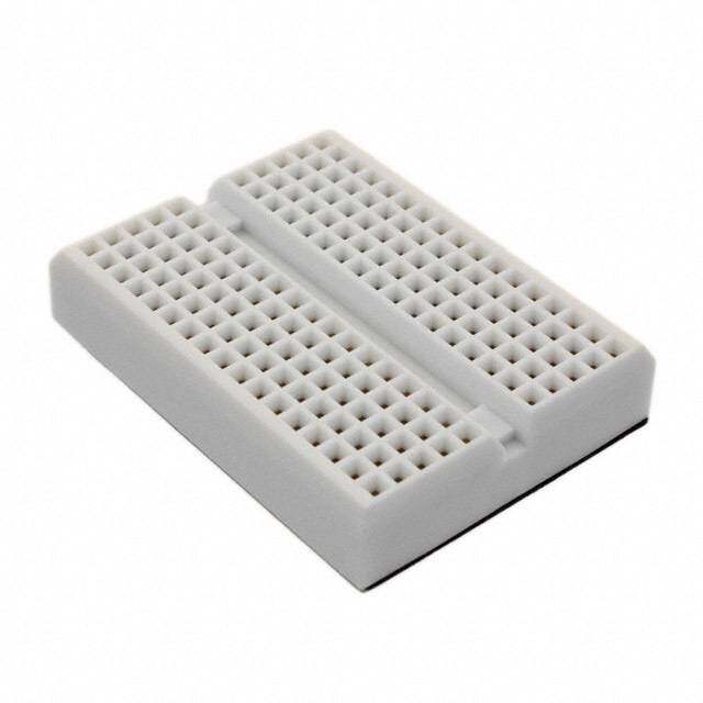
Document Reference No.: FT_000327 Vinco Development Module Datasheet Version 2.01 Clearance No.: FTDI#173 10 Arduino Shields The Vinculo module has the same form factor as the Arduino Duemilanove under the terms of the Creative Commons Attribution Share-Alike license, which allows for both personal and commercial derivative works. This allows for other Arduino compatible shields to mate directly to the Vinculo PCB. In addition to the existing shields on the market, a bare shield with a prototyping area, Vinco_Proto, is also available to enable users to make their own shield. This shield includes connectors and an assortment of resistors and LEDs to provide a starting point aimed at the hobbyist. Figure 10.1 – Vinco_Proto Copyright © 2012 Future Technology Devices International Limited 17
Document Reference No.: FT_000327 Vinco Development Module Datasheet Version 2.01 Clearance No.: FTDI#173 11 Contact Information Head Office – Glasgow, UK Branch Office – Hillsboro, Oregon, USA Future Technology Devices International Limited 7130 SW Fir Loop Unit 1, 2 Seaward Place, Tigard, OR 97223 Centurion Business Park USA Glasgow, G41 1HH Tel: +1 (503) 547 0988 United Kingdom Fax: +1 (503) 547 0987 Tel: +44 (0) 141 429 2777 Fax: +44 (0) 141 429 2758 E-Mail (Sales) us.sales@ftdichip.com E-Mail (Support) us.support@ftdichip.com E-Mail (General Enquiries) us.admin@ftdichip.com E-mail (Sales) sales1@ftdichip.com E-mail (Support) support1@ftdichip.com Branch Office – Shanghai, China E-mail (General Enquiries) admin1@ftdichip.com Room 408, 317 Xianxia Road, Branch Office – Taipei, Taiwan ChangNing District, ShangHai, China 2F, No 516, Sec. 1 NeiHu Road Taipei 114 Tel: +86 (21) 62351596 Taiwan, R.O.C. Fax: +86(21) 62351595 Tel: +886 (0) 2 8791 3570 Fax: +886 (0) 2 8791 3576 E-Mail (Sales): cn.sales@ftdichip.com E-Mail (Support): cn.support@ftdichip.com E-mail (Sales) tw.sales1@ftdichip.com E-Mail (General Enquiries): cn.admin1@ftdichip.com E-mail (Support) tw.support1@ftdichip.com E-mail (General Enquiries) tw.admin1@ftdichip.com Web Site URL Distributor and Sales Representatives Please visit the Sales Network page of the FTDI Web site for the contact details of our distributor(s) and sales representative(s) in your country. System and equipment manufacturers and designers are responsible to ensure that their systems, and any Future Technology Devices International Ltd (FTDI) devices incorporated in their systems, meet all applicable safety, regulatory and system-level performance requirements. All application-related information in this document (including application descriptions, suggested FTDI devices and other materials) is provided for reference only. While FTDI has taken care to assure it is accurate, this information is subject to customer confirmation, and FTDI disclaims all liability for system designs and for any applications assistance provided by FTDI. Use of FTDI devices in life support and/or safety applications is entirely at the user’s risk, and the user agrees to defend, indemnify and hold harmless FTDI from any and all damages, claims, suits or expense resulting from such use. This document is subject to change without notice. No freedom to use patents or other intellectual property rights is implied by the publication of this document. Neither the whole nor any part of the information contained in, or the product described in this document, may be adapted or reproduced in any material or electronic form without the prior written consent of the copyright holder. Future Technology Devices International Ltd, Unit 1, 2 Seaward Place, Centurion Business Park, Glasgow G41 1HH, United Kingdom. Scotland Registered Company Number: SC136640 Copyright © 2012 Future Technology Devices International Limited 18
Document Reference No.: FT_000327 Vinco Development Module Datasheet Version 2.01 Clearance No.: FTDI#173 Appendix A – References VNC2 Datasheet Vinculum-II Errata Technical Note Application and Technical Notes available at http://www.ftdichip.com/Support/Documents/AppNotes.htm Vinculum-II IO Cell Description Vinculum-II Debug Interface Description Vinculum-II IO Mux Explained Vinculum-II PWM Example Migrating Vinculum Designs From VNC1L to VNC2-48L1A Vinculum-II Toolchain Installation Guide Vinculum-II Toolchain Getting Started Guide Vinculum-II User Guide MCP3008 Datasheet (http://ww1.microchip.com/downloads/en/DeviceDoc/21295d.pdf) Copyright © 2012 Future Technology Devices International Limited 19
Document Reference No.: FT_000327 Vinco Development Module Datasheet Version 2.01 Clearance No.: FTDI#173 Appendix B – List of Figures and Tables List of Figures Figure 1.1 – VINCO ....................................................................................................................... 1 Figure 3.1 – Vinco Diagram ............................................................................................................ 4 Figure 8.1 – Vinco Dimensions ..................................................................................................... 15 Figure 8.2 – Vinco Pitch Measurements ......................................................................................... 15 Figure 9.1 – Vinco Schematics ...................................................................................................... 16 Figure 10.1 – Vinco_Proto ............................................................................................................ 17 List of Tables Table 1.1 – Vinco Part Numbers ...................................................................................................... 3 Table 3.1 – Vinco Connector Descriptions ........................................................................................ 4 Table 3.2 – Pin Signal Descriptions ................................................................................................. 6 Table 3.3 – USB Slave Pin Out ........................................................................................................ 7 Table 3.4 – USB Slave Pin Out ........................................................................................................ 7 Table 3.5 – Jumper Options ........................................................................................................... 8 Table 4.1 – Data and Control Bus Signal Mode Options – UART........................................................... 9 Table 4.2 – Data and Control Bus Signal Mode Options – SPI Slave ................................................... 10 Table 4.3 – Data and Control Bus Signal Mode Options – SPI Master ................................................. 10 Table 4.4 – Data and Control Bus Signal Mode Options – Parallel FIFO Interface ................................. 11 Table 5.1 – Signal Name and Description – Debugger Interface ........................................................ 12 Table 6.1 – ADC Interface ............................................................................................................ 13 Copyright © 2012 Future Technology Devices International Limited 20
Document Reference No.: FT_000327 Vinco Development Module Datasheet Version 2.01 Clearance No.: FTDI#173 Appendix C – Revision History Document Title: Vinco Development Module Document Reference No.: FT_000327 Clearance No.: FTDI#173. Product Page: http://www.ftdichip.com/Products/Modules/DevelopmentModules.htm Document Feedback: Send Feedback Version 1.0 First Release October 13th 2010 Version 1.1 Added images of Vinculo_Proto October 20th 2010 Version 1.2 Changed text about software in introduction October 28th 2010 Version 1.3 Added text about default/initial state of the Vinculo module December 24th 2010 default/initial state of the Vinculo module Updated the disclaimer. Renamed the debugger module to VNC2 debugger/programming module. Section 1: Added text about debugger/programmer module Section 1.3: Added part number VNCLO-START1 Updated table 3.1(Description), 4.1, 4.2, 4.3 and 4.4 (Available pins) Version 1.4 Added part number VNCLO-PREM1 January 28th 2011 Version 1.5 Updated schematic and tables and corrected reference designator March 18th 2011 Added a simplified dimentions drawing Version 2.0 Updated product name to Vinco April 11th 2011 Updated table formatting Added LED1, LED2 and PWREN# GPIO locations with respect to VNC2 pins Version 2.01 Corrected Figure 3.1 pin 1 location on J3 to J6 Dec 14th 2012 Note added under figure 9.1 on power control Copyright © 2012 Future Technology Devices International Limited 21
Mouser Electronics Authorized Distributor Click to View Pricing, Inventory, Delivery & Lifecycle Information: F TDI: VNCLO-MB1A VNCLO-PSU-UK VNCLO-PSU-USA VNCLO-PSU-EU VNCLO-SHLD-1A