ICGOO在线商城 > V2AF118A400Y2EDP
- 型号: V2AF118A400Y2EDP
- 制造商: AVX
- 库位|库存: xxxx|xxxx
- 要求:
| 数量阶梯 | 香港交货 | 国内含税 |
| +xxxx | $xxxx | ¥xxxx |
查看当月历史价格
查看今年历史价格
V2AF118A400Y2EDP产品简介:
ICGOO电子元器件商城为您提供V2AF118A400Y2EDP由AVX设计生产,在icgoo商城现货销售,并且可以通过原厂、代理商等渠道进行代购。 提供V2AF118A400Y2EDP价格参考以及AVXV2AF118A400Y2EDP封装/规格参数等产品信息。 你可以下载V2AF118A400Y2EDP参考资料、Datasheet数据手册功能说明书, 资料中有V2AF118A400Y2EDP详细功能的应用电路图电压和使用方法及教程。
| 参数 | 数值 |
| 产品目录 | |
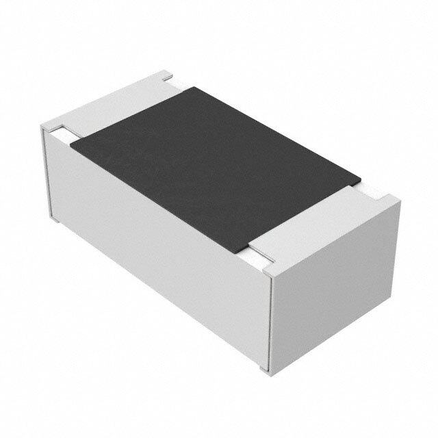
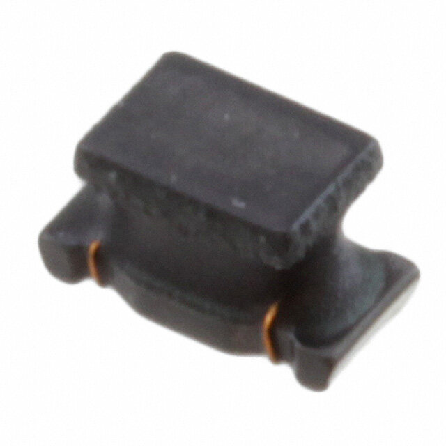
| 描述 | VARISTOR 30A 0805压敏电阻 18Vdc 42volts 30A 0805 |
| 产品分类 | |
| 品牌 | AVX |
| 产品手册 | |
| 产品图片 | |
| rohs | 符合RoHS无铅 / 符合限制有害物质指令(RoHS)规范要求 |
| 产品系列 | AVX V2AF118A400Y2EDPTransGuard® |
| mouser_ship_limit | 该产品可能需要其他文档才能发货到中国。 |
| 数据手册 | |
| 产品型号 | V2AF118A400Y2EDP |
| 产品 | MLV |
| 产品种类 | 压敏电阻 |
| 其它名称 | 478-9362-6 |
| 包装 | Digi-Reel® |
| 变阻器电压 | 22.95V |
| 商标 | AVX |
| 商标名 | TransGuard |
| 外壳代码-in | 0805 |
| 外壳代码-mm | 2012 |
| 外壳宽度 | 1.25 mm |
| 安装 | SMD/SMT |
| 容差 | - 50 %, + 100 % |
| 宽度 | 1.25 mm |
| 封装 | Reel |
| 封装/外壳 | 0805(2012 公制) |
| 封装/箱体 | 0805 (2012 metric) |
| 尺寸 | 1.25 mm W |
| 峰值浪涌电流 | 30 A |
| 工作温度范围 | - 55 C to + 125 C |
| 工厂包装数量 | 1000 |
| 最大AC电压 | 13VAC |
| 最大DC电压 | 18VDC |
| 标准包装 | 1 |
| 浪涌能量额定值 | 0.1 J |
| 电压 | 18 VDC |
| 电压额定值AC | 13 V |
| 电压额定值DC | 18 V |
| 电容 | 200 pF |
| 电流-浪涌 | 30A |
| 电流额定值 | 750 mA |
| 电路数 | 1 |
| 端接类型 | SMD/SMT |
| 系列 | V2AF |
| 能量 | 0.10J |
| 钳位电压 | 42 V |



- 商务部:美国ITC正式对集成电路等产品启动337调查
- 曝三星4nm工艺存在良率问题 高通将骁龙8 Gen1或转产台积电
- 太阳诱电将投资9.5亿元在常州建新厂生产MLCC 预计2023年完工
- 英特尔发布欧洲新工厂建设计划 深化IDM 2.0 战略
- 台积电先进制程称霸业界 有大客户加持明年业绩稳了
- 达到5530亿美元!SIA预计今年全球半导体销售额将创下新高
- 英特尔拟将自动驾驶子公司Mobileye上市 估值或超500亿美元
- 三星加码芯片和SET,合并消费电子和移动部门,撤换高东真等 CEO
- 三星电子宣布重大人事变动 还合并消费电子和移动部门
- 海关总署:前11个月进口集成电路产品价值2.52万亿元 增长14.8%
PDF Datasheet 数据手册内容提取
TransFeed Automotive Series AVX Multilayer Ceramic Transient Voltage Suppressors TVS Protection and EMI Attenuation in a Single Chip GENERAL DESCRIPTION Schematic Diagram AVX has combined the best electrical characteristics of its TransGuard® Transient Voltage Suppressors (TVS) and its IN OUT Feedthru Capacitors into a single chip for state-of-the-art overvoltage circuit protection and EMI reduction over a broad range of frequencies. This unique combination of Electrical Model multilayer ceramic construction in a feedthru configuration gives the circuit designer a single 0805 chip that responds to transient events faster than any TVS device on the mar- IN LS LS OUT ket today, and provides significant EMI attenuation when in the off-state. RV C RP Automotive TransFeeds are designed for automotive appli- RON cations and are AEC-Q 200 qualified. The reduction in parallel inductance, typical of the feedthru LP chip construction when compared to the construction of standard TVS or ceramic capacitor chips, gives the TransFeed product two very important electrical advan- inductance, is the enhanced attenuation characteristics of tages: (1) faster “turn-on” time. Calculated response times the TransFeed product. Not only is there significantly of <200 pSec are not unusual with this device, and mea- greater attenuation at a higher self-resonance frequency, sured response times range from 200 – 250 pSec. The but the roll-off characteristic becomes much flatter, result- TransFeed “turn-on” characteristic is less than half that of ing in EMI filtering over a much broader frequency spec- an equivalent TransGuard® part — and TransGuards® trum. Typical applications include filtering/protection on clamp transient voltages faster than any other bipolar TVS Microcontroller I/O Lines, Interface I/O Lines, Power Line solution such as diodes; (2) the second electrical advantage Conditioning and Power Regulation. of lower parallel inductance, coupled with optimal series TYPICAL APPLICATIONS GENERAL FEATURES CHARACTERISTICS • Drive by Wire • Bi-directional TVS • Dimming Mirror Circuit • Operting Teperature: -55°C to +125°C • Narrow band, high • Filtering/protection on Microcontroller I/O lines • Working Voltage: 5.6Vdc - 26Vdc attenuation filter • Filtering/protection on Interface I/O lines • Case Size: 0805 • EMI Filtering over broader • Power Line Conditioning • Energy Rating: 0.05 - 0.3J frequency range • Power Regulation • Current: 20 - 120A • Fastest Response Time to • LCD Dashboard driver • Max Feedthru Current: 0.5 - 1A ESD Strikes • AEC-Q 200 Qualified Where designers are concerned with both tran- sient voltage protection and EMI attenuation, either due to the electrical performance of their circuits or due to required compliance to specif- ic EMC regulations, the TransFeed product is an ideal choice. 90 080216
TransFeed Automotive Series AVX Multilayer Ceramic Transient Voltage Suppressors TVS Protection and EMI Attenuation in a Single Chip HOW TO ORDER V 2 AF 1 05 A 150 Y 2 E D P Varistor Automotive Voltage Varistor DC Packaging Feedthru 05 =5.6VDC Clamping Resistance Code Capacitor 09 =9.0VDC Voltage 1 = 0.150 Ohms Pcs./Reel 14 = 14.0VDC 150 = 18V 2 = 0.200 Ohms D = 1,000 18 = 18.0VDC 200 = 22V 3 = 0.250 Ohms R = 4,000 26 = 26.0VDC 300 = 32V T = 10,000 400 = 42V 500 = 50V Chip Size No. of Energy 600 = 60V Capaci tance Feedthru Termination Finish 2 = 0805 Elements Rating Tolerance Current P = Ni/Sn (Plated) X = 0.05J Y = +100/-50% D = 500 mA A = 0.1J E = 750 mA C = 0.3J F = 1.0 Amp TRANSFEED ELECTRICAL SPECIFICATIONS AVX Working Working Breakdown Clamping Maximum Transient Peak Typical DC Maximum Jump Part Number Voltage Voltage Voltage Voltage Leakage Energy Current Cap Resistance Feedthru Start (DC) (AC) Current Rating Rating Current Voltage V2AF105A150Y2E _ _ 5.6 4.0 8.5±20% 18 35 0.10 30 800 0.200 0.75 – V2AF105C150Y1F _ _ 5.6 4.0 8.5±20% 18 35 0.30 120 2500 0.150 1.00 – V2AF109A200Y2E _ _ 9.0 6.4 12.7±15% 22 25 0.10 30 575 0.200 0.75 – V2AF109C200Y1F _ _ 9.0 6.4 12.7±15% 22 25 0.30 120 1800 0.150 1.00 – V2AF114A300Y2E _ _ 14.0 10.0 18.5±12% 32 15 0.10 30 300 0.200 0.75 27.5 V2AF114C300Y1F _ _ 14.0 10.0 18.5±12% 32 15 0.30 120 900 0.150 1.00 27.5 V2AF118A400Y2E _ _ 18.0 13.0 25.5±10% 42 10 0.10 30 200 0.200 0.75 27.5 V2AF118C400Y1F _ _ 18.0 13.0 25.5±10% 42 10 0.30 120 500 0.150 1.00 27.5 V2AF118X500Y3D _ _ 18.0 13.0 25.5±10% 50 10 0.05 20 75 0.250 0.50 27.5 V2AF126C600Y2E_ _ 26.0 18.0 34.5±10% 60 10 0.3 80 250 0.2 0.75 27.5 Termination Finish Code Packaging Code V (DC) DC Working Voltage (V) E Transient Energy Rating (J, 10x1000μS) W T V (AC) AC Working Voltage (V) I Peak Current Rating (A, 8x20μS) W P V Typical Breakdown Voltage (V @ 1mA ) Cap Typical Capacitance (pF) @ 1MHz and 0.5 V B DC V Tol V Tolerance is ± from Typical Value DCR DC Resistance (Ohms) B B V Clamping Voltage (V @ 1A 8x20μS) I Maximum Feedthru Current (A) C FT I Maximum Leakage Current at the Working Voltage (μA) V Jump Start Voltage (V, 5 min) L JUMP 080216 91
TransFeed Automotive Series AVX Multilayer Ceramic Transient Voltage Suppressors TVS Protection and EMI Attenuation in a Single Chip DIMENSIONS mm (inches) L W T BW BL EW X S 2.01 ± 0.20 1.25 ± 0.20 1.143 Max. 0.46 ± 0.10 0.18 + 0.25 -0.08 0.25 ± 0.13 1.02 ± 0.10 0.23 ± 0.05 0805 (0.079 ± 0.008) (0.049 ± 0.008) (0.045 Max.) (0.018 ± 0.004) (0.007 + 0.010 -0.003) (0.010 ± 0.005) (0.040 ± 0.004) (0.009 ± 0.002) L X S T BW CL BL W EW RECOMMENDED SOLDER PAD LAYOUT (Typical Dimensions) mm (inches) T P S W L C 0805 3.45 (0.136) 0.51 (0.020) 0.76 (0.030) 1.27 (0.050) 1.02 (0.040) 0.46 (0.018) 4 Pad Layout T P P S W INPUT OUTPUT C L 92 080216
TransFeed Automotive Series AVX Multilayer Ceramic Transient Voltage Suppressors TVS Protection and EMI Attenuation in a Single Chip PERFORMANCE CHARACTERISTICS FEEDTHRU VARISTORS AVX Multilayer Feedthru Varistors (MLVF) are an ideal choice The electrical model for a ZnO MLV and a ZnO Feedthru MLV for system designers with transient strike and broadband are shown below. The key difference in the model for EMI/RFI concerns. the Feedthru is a transformation in parallel to series induc- Feedthru Varistors utilize a ZnO varistor material and the tance. The added series inductance helps lower the injected electrode pattern of a feedthru capacitor. This combination transient peak current (by 2πfL) resulting in an additional ben- allows the package advantage of the feedthru and material efit of a lower clamping voltage. The lowered parallel induc- advantages of the ZnO dielectric to be optimized. tance decreases the turn on time for the varistor to <250ps. ZnO MLV Feedthrus exhibit electrical and physical advantages over standard ZnO MLVs. Among them are: 1. Faster Turn on Time 2. Broadband EMI attenuation 3. Small size (relative to discrete MLV and EMI filter schemes) Discrete MLV Model Discrete MLVF Model To Device To Device PCB Requiring Requiring Trace Protection Protection LS LS Solder Pad Solder Pad LP RV C RP RV C RP Ron Ron LP Solder Pad Solder Pad Where: Rv = Voltage Variable resistance Where: Rv = Voltage Variable resistance (per VI curve) (per VI curve) Rp ≥ 1012Ω Rp = Body IR C = defined by voltage rating and energy level C = defined by voltage rating and energy level Ron = turn on resistance Ron = turn on resistance Lp = parallel body inductance Lp = minimized parallel body inductance Ls = series body inductance 080216 93
TransFeed Automotive Series AVX Multilayer Ceramic Transient Voltage Suppressors TVS Protection and EMI Attenuation in a Single Chip PERFORMANCE CHARACTERISTICS APPLICATIONS MARKET SEGMENTS TYPICAL CIRCUITS REQUIRING • EMI Suppression • Computers TRANSIENT VOLTAGE • Broadband I/O Filtering • Automotive PROTECTION AND EMI FILTERING • Vcc Line Conditioning • Power Supplies • Multimedia Add-On Cards The following applications and schematic diagrams FEATURES • Bar Code Scanners show where TransFeed TVS/ EMI filtering devices might • Remote Terminals be used: • Small Size • Medical Instrumentation • System Board Level Interfaces: (Fig. 1) • Low ESR • Test Equipment Digital to RF • Ultra-fast Response Time • Transceivers Analog to Digital • Broad S21 Characteristics • Cellular Phones / Pagers Digital to Analog • Voltage Regulation (Fig. 2) • Power Conversion Circuits (Fig. 3) • GaAs FET Protection (Fig. 4) Fig. 1 – System Interface Fig. 2 – Voltage Regulators REGULATOR + Sensor/Keyboard/ Touchscreen Input DBIOGAIRTDAL(cid:31) RF BOARD By X Bus Fig. 3 – Power Conversion Circuits/Power Switching Circuits +3.3V MAIN(cid:31) POWER(cid:31) INTERFACE(cid:31) POWER MANAGE(cid:31)MENT(cid:31) +3.3V CARD Sensor Input ANALOG(cid:31) DIGITAL(cid:31) Display CHIP BOARD BOARD +5V +1.8V +12V Keyboard DIGITAL(cid:31) ANALOG(cid:31) ASIC BOARD BOARD Fig. 4 – GaAs FET Protection SPECIFICATION COMPARISON INPUT OUTPUT MLVF PARAMETER MLV 0805 0805 5ph Ls typical N/A <600nh Lp typical <1.5nh <0.025Ω Ron typical <0.1Ω Fig. 5 – Automotive TransFeed - Throttle by Wire 100pf to 2.5nf C typical 100pf to 5.5nf see VI curves Rv typical see VI curves THROTTLE >0.25 x 10¹²Ω Rp typical >1 x 10¹²Ω ACCELERATOR DRIVE SENSOR <250ps Typical turn on time <500ps ECU Typical frequency response A comparison table showing typical element parameters and resulting THROTTLE performance features for MLV and MLVF is shown above. SENSOR 94 080216
Mouser Electronics Authorized Distributor Click to View Pricing, Inventory, Delivery & Lifecycle Information: A VX: V2AF118A400Y2EDP V2AF105C150Y1FDP V2AF114C300Y1FDP V3AF418A400Y3GDP V2AF109C200Y1FDP V2AF118X500Y3DDP V2AF109A200Y2EDP V2AF118C400Y1FDP V2AF105A150Y2EDP V2AF114A300Y2EDP V3AF418X500Y3GDP V2AF118C400Y1FRP V2AF114C300Y1FRP V2AF114A300Y2ERP V2AF118C400Y1FTP V2AF105A150Y2ETP V2AF109C200Y1FTP V2AF118X500Y3DTP V2AF105C150Y1FTP V2AF109C200Y1FRP V2AF118A400Y2ETP V2AF118X500Y3DRP V2AF114C300Y1FTP V2AF105C150Y1FRP V2AF109A200Y2ETP V2AF114A300Y2ETP V3AF418A400Y3GRP V2AF105A150Y2ERP V3AF418X500Y3GTP V3AF418X500Y3GRP V3AF418A400Y3GTP V2AF109A200Y2ERP V2AF118A400Y2ERP V2AF126C600Y2EDP V2F126C600Y2ERP

 Datasheet下载