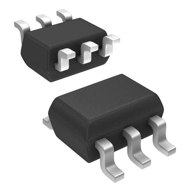
ICGOO在线商城 > 滤波器 > EMI/RFI 滤波器(LC,RC 网络) > USBUF02W6
- 型号: USBUF02W6
- 制造商: STMicroelectronics
- 库位|库存: xxxx|xxxx
- 要求:
| 数量阶梯 | 香港交货 | 国内含税 |
| +xxxx | $xxxx | ¥xxxx |
查看当月历史价格
查看今年历史价格
USBUF02W6产品简介:
ICGOO电子元器件商城为您提供USBUF02W6由STMicroelectronics设计生产,在icgoo商城现货销售,并且可以通过原厂、代理商等渠道进行代购。 USBUF02W6价格参考¥0.99-¥0.99。STMicroelectronicsUSBUF02W6封装/规格:EMI/RFI 滤波器(LC,RC 网络), RC (Pi) EMI Filter 2nd Order Low Pass 2 Channel R = 22 Ohms, C = 47pF 6-TSSOP, SC-88, SOT-363。您可以下载USBUF02W6参考资料、Datasheet数据手册功能说明书,资料中有USBUF02W6 详细功能的应用电路图电压和使用方法及教程。
STMicroelectronics的USBUF02W6是一款专为EMI/RFI(电磁干扰/射频干扰)滤波设计的LC网络器件。它主要用于抑制电源线和信号线中的高频噪声,确保电子设备在复杂电磁环境中稳定运行。

 应用场景:

1. 消费电子设备:
   - 该器件广泛应用于各类消费电子产品中,如智能手机、平板电脑、智能手表等便携式设备。这些设备通常需要在有限的空间内集成多种功能模块,因此对外部电磁干扰的防护要求较高。USBUF02W6能够有效减少高频噪声对内部电路的影响,提升设备的稳定性和可靠性。

2. 通信设备:
   - 在通信基站、路由器、调制解调器等设备中,USBUF02W6可以用于保护敏感的射频前端电路。它能有效过滤掉来自电源线或信号线的高频噪声,确保信号传输的纯净度,提高通信质量,减少误码率。

3. 汽车电子系统:
   - 现代汽车中集成了大量的电子控制系统,如发动机控制单元(ECU)、车载娱乐系统、高级驾驶辅助系统(ADAS)等。USBUF02W6可以用于这些系统的电源输入端,防止外界电磁干扰影响车辆的安全性和性能。

4. 工业自动化设备:
   - 在工业环境中,电机驱动器、PLC控制器、传感器等设备容易受到电磁干扰的影响。USBUF02W6可以帮助这些设备抵御外部干扰,确保工业生产线的稳定运行,减少故障停机时间。

5. 医疗设备:
   - 医疗设备对电磁兼容性有严格的要求,特别是在医院等环境中,各种设备密集使用,电磁环境复杂。USBUF02W6可以用于医疗设备的电源输入和信号接口处,确保设备的正常工作,保障患者安全。

总之,USBUF02W6凭借其高效的EMI/RFI滤波性能,适用于多种需要高可靠性和抗干扰能力的应用场合,特别适合那些对电磁兼容性要求较高的电子设备。
| 参数 | 数值 |
| 产品目录 | |
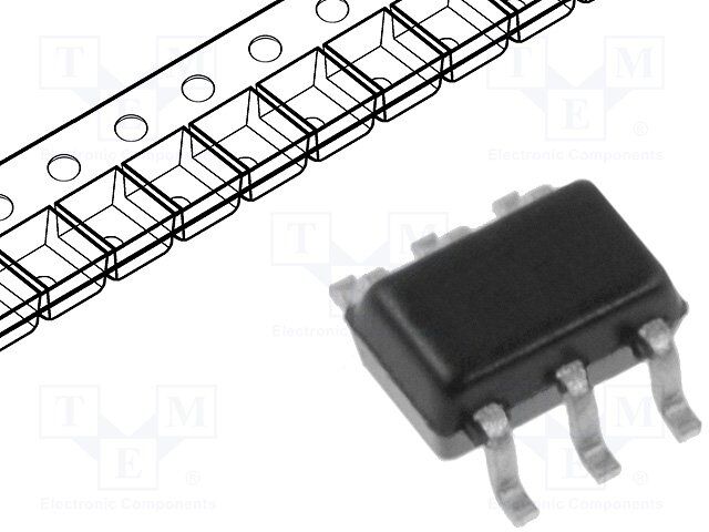
| 描述 | IC EMI FILTER/LINE TERM SOT323-6EMI滤波珠子、芯片与阵列 EMI FILTER IPAD |
| ESD保护 | 是 |
| 产品分类 | EMI/RFI 滤波器(LC、RC 网络)EMI/RFI 器件 |
| 品牌 | STMicroelectronics |
| 产品手册 | |
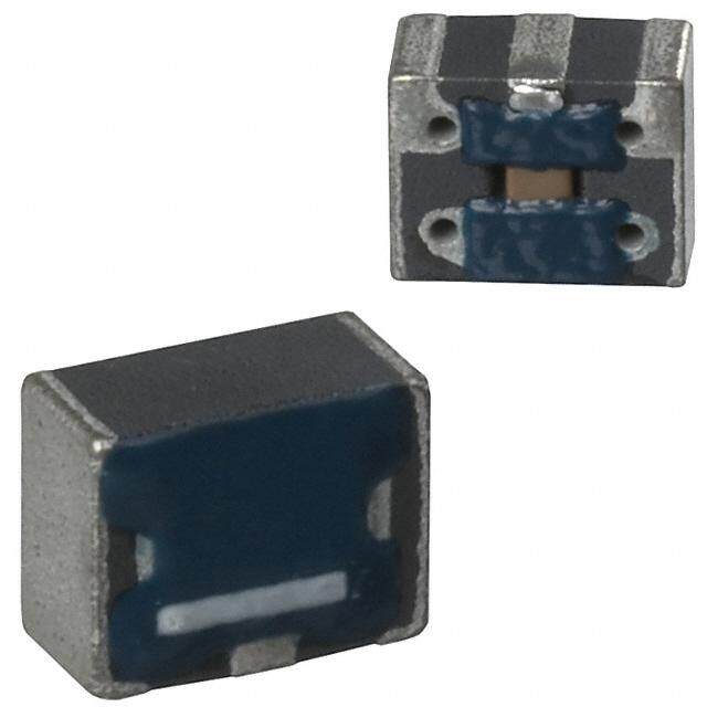
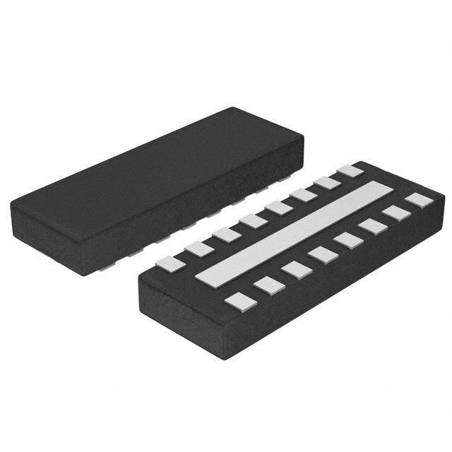
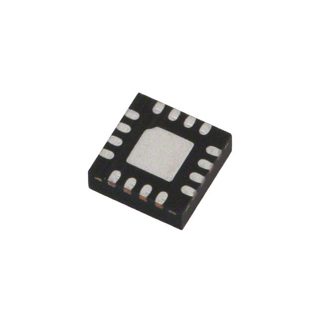
| 产品图片 |
|
| rohs | 符合RoHS无铅 / 符合限制有害物质指令(RoHS)规范要求 |
| 产品系列 | EMI滤波珠子、芯片与阵列,STMicroelectronics USBUF02W6ASD |
| 数据手册 | |
| 产品型号 | USBUF02W6 |
| 中心/截止频率 | - |
| 产品 | EMI Filter Arrays |
| 产品目录页面 | |
| 产品种类 | EMI滤波珠子、芯片与阵列 |
| 其它名称 | 497-3743-2 |
| 其它有关文件 | http://www.st.com/web/catalog/sense_power/FM139/CL1432/SC1434/PF65578?referrer=70071840 |
| 包装 | 带卷 (TR) |
| 商标 | STMicroelectronics |
| 外壳宽度 | 1.35 mm |
| 外壳长度 | 2.2 mm |
| 外壳高度 | 1.1 mm |
| 大小/尺寸 | 0.079" 长 x 0.049" 宽(2.00mm x 1.25mm) |
| 容差 | 10 % |
| 封装 | Reel |
| 封装/外壳 | 6-TSSOP,SC-88,SOT-363 |
| 封装/箱体 | SOT-323-6L |
| 尺寸 | 1.35 mm W x 2.2 mm L x 1.1 mm H |
| 工作温度 | -40°C ~ 70°C |
| 工作温度范围 | - 40 C to + 70 C |
| 工厂包装数量 | 3000 |
| 应用 | USB |
| 技术 | RC(Pi) |
| 数值 | R = 22 欧姆,C = 47pF |
| 最大直流电阻 | 33 Ohms |
| 标准包装 | 3,000 |
| 测试频率 | 30 MHz to 1 GHz |
| 滤波器阶数 | 2nd |
| 电流 | - |
| 电阻-通道(Ω) | 22 |
| 端接类型 | SMD/SMT |
| 类型 | 低通 |
| 系列 | USBUF |
| 衰减值 | - |
| 通道数 | 2 |
| 频率范围 | 30 MHz to 1 GHz |
| 高度 | 0.043"(1.10mm) |



- 商务部:美国ITC正式对集成电路等产品启动337调查
- 曝三星4nm工艺存在良率问题 高通将骁龙8 Gen1或转产台积电
- 太阳诱电将投资9.5亿元在常州建新厂生产MLCC 预计2023年完工
- 英特尔发布欧洲新工厂建设计划 深化IDM 2.0 战略
- 台积电先进制程称霸业界 有大客户加持明年业绩稳了
- 达到5530亿美元!SIA预计今年全球半导体销售额将创下新高
- 英特尔拟将自动驾驶子公司Mobileye上市 估值或超500亿美元
- 三星加码芯片和SET,合并消费电子和移动部门,撤换高东真等 CEO
- 三星电子宣布重大人事变动 还合并消费电子和移动部门
- 海关总署:前11个月进口集成电路产品价值2.52万亿元 增长14.8%

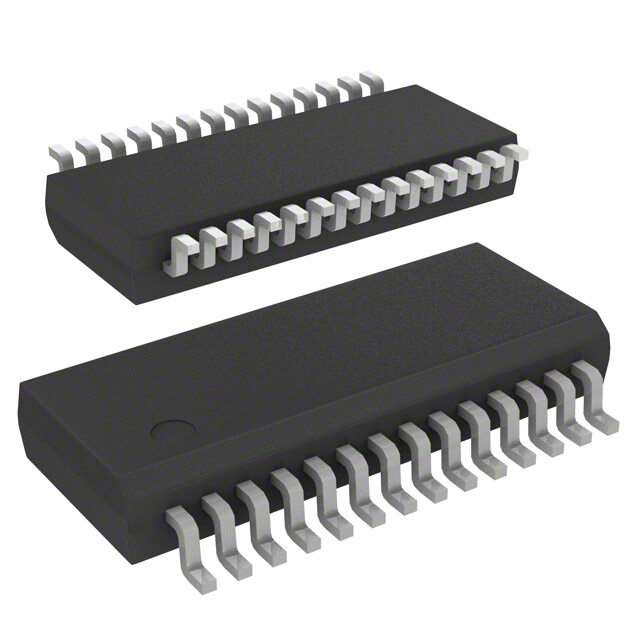

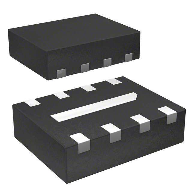
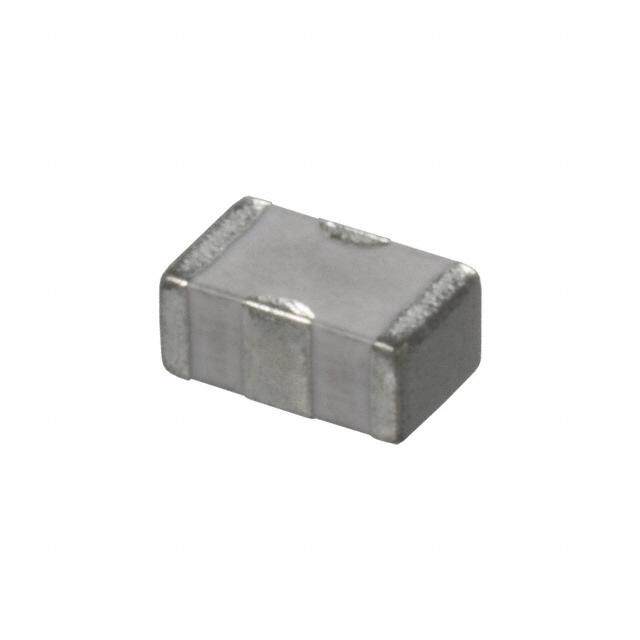

PDF Datasheet 数据手册内容提取
USBUF EMI filter and line termination for USB upstream ports Datasheet - production data • Complies with the following standards IEC 61000-4-2, level 4 – ± 15 kV (air discharge) – ± 8 kV (contact discharge) – MIL STD 883E, Method 3015-7 SOT323-6L – Class 3 C = 100 pF; R = 1500 Ω – 3 positive strikes and 3 negative strikes (F= 1 Hz) Application Figure 1. Functional diagram EMI Filter and line termination for USB upstream 3.3V ports on: Rt Rp D1 D4 • USB Hubs Ct • PC peripherals Grd 3.3V Description The USB specification requires upstream ports to Rt be terminated with pull-up resistors from the D+ D2 D3 and D- lines to Vbus. On the implementation of Ct USB systems, the radiated and conducted EMI should be kept within the required levels as stated by the FCC regulations. In addition to the requirements of termination and EMC Features compatibility, the computing devices are required • Monolithic device with recommended line to be tested for ESD susceptibility. termination for USB upstream ports The USBUF provides the recommended line • Integrated Rt series termination and Ct termination while implementing a low pass filter to limit EMI levels and providing ESD protection bypassing capacitors. which exceeds IEC 61000-4-2 level 4 standard. • Integrated ESD protection The device is packaged in a SOT323-6L which is • Small package size the smallest available lead frame package (50% • Benefits smaller than the standard SOT23). – EMI / RFI noise suppression Table 1. Device summary – Required line termination for USB upstream ports Order codes Marking – ESD protection exceeding IEC 61000-4-2 USBUF01W6 UU1 level4 USBUF02W6 UU2 – High flexibility in the design of high density boards – Tailored to meet USB 1.1 standard August 2015 DocID7041 Rev 8 1/13 This is information on a product in full production. www.st.com
Characteristics USBUF 1 Characteristics Table 2. Absolute ratings (T = 25° C) amb Symbol Parameter Value Unit ESD discharge IEC 61000-4-2, air discharge ±16 V ESD discharge IEC 61000-4-2, contact discharge ±9 kV PP ESD discharge - MIL STD 883E - Method 3015-7 ±25 Tj Maximum junction temperature 150 °C Tstg Storage temperature range - 55 to + 150 °C TL Lead solder temperature (10 second duration) 260 °C Top Operating temperature range -40 to 125 °C P Power rating per resistor 100 mW Table 3. Functional diagram Rt Rp Ct CODE 01 33 W 1.5 kΩ 47 pF CODE 02 22 W 1.5 kΩ 47 pF Tolerance ± 10% ± 10% ± 20% 2/13 DocID7041 Rev 8
USBUF Technical information 2 Technical information Figure 2. USB standard requirements 3.3V 1.5k Rt D+ D+ Rt Full-speed or Low-speed USB Ct Twisted pair shielded Ct Full-speed USB Transceiver Rt Rt Transceiver D- Zo = 90ohms D- Ct 15k 15k 5m max Ct Host or Hub 0 or Hub port Full-speed function FULL SPEED CONNECTION 3.3V 1.5k Rt D+ D+ Rt Full-speed or Low-speed USB Ct Untwisted unshielded Ct LTroawn-sscpeeiveedr USB Transceiver Rt Rt D- 3m max D- Host or Ct 15k 15k Ct Hub 0 or Hub port Low-speed function LOW SPEED CONNECTION DocID7041 Rev 8 3/13 13
Technical information USBUF 2.1 Application example Figure 3. Implementation of ST solutions for USB ports USBUF01W6 Downstream port USBDF01W5 Upstreamport D2 Gnd D1 D+ Host/Hub USB por transceivert DDG+-nd DDG+-n iinnd CCttRRttRRdd DD+- oouutt DD+- CABLE DD+- Ct RDt3 3.C3Vt RRD3pt.43V D- Peripheral transceiver FULL SPEED CONNECTION USBUF01W6 Downstream port USBDF01W5 Upstreamport D+ D2 Gnd D1 Host/Hub USB por transceivert DDG+-nd DDG+-n iinnd CCttRRttRRdd DD+- oouutt DD+- CABLE DD+- Ct RDt3 3.C3Vt RRD3pt.43V D- Peripheral transceiver LOW SPEED CONNECTION 2.2 EMI filtering Current FCC regulations requires that class B computing devices meet specified maximum levels for both radiated and conducted EMI. • Radiated EMI covers the frequency range from 30 MHz to 1 GHz. • Conducted EMI covers the 450 kHz to 30 MHz range. For the types of devices utilizing the USB, the most difficult test to pass is usually the radiated EMI test. For this reason the USBUF device is aiming to minimize radiated EMI. The differential signal (D+ and D-) of the USB does not contribute significantly to radiated or conducted EMI because the magnetic field of both conductors cancels each other. The inside of the PC environment is very noisy and designers must minimize noise coupling from the different sources. D+ and D-must not be routed near high speed lines (clocks spikes). Induced common mode noise can be minimized by running pairs of USB signals parallel to each other and running grounded guard trace on each side of the signal pair from the USB controller to the USBUF device. If possible, locate the USBUF device physically near the 4/13 DocID7041 Rev 8
USBUF Technical information USB connectors. Distance between the USB controller and the USB connector must be minimized. The 47 pF (C) capacitors are used to bypass high frequency energy to ground and for edge t control, and are placed between the driver chip and the series termination resistors (Rt). Both Ct and Rt should be placed as close to the driver chip as is practicable. The USBUF ensures a filtering protection against Electromagnetic and Radio-frequency Interferences thanks to its low-pass filter structure. This filter is characterized by the following parameters: • cut-off frequency • Insertion loss • high frequency rejection. Figure 4. USBUF typical attenuation Figure 5. Measurement configuration S21 (dB) 0 -10 50Ω TEST BOARD UUx -20 Vg 50Ω -30 1 10 100 1,000 Frequency (MHz) 2.3 ESD protection In addition to the requirements of termination and EMC compatibility, computing devices are required to be tested for ESD susceptibility. This test is described in the IEC 61000-4-2 and is already in place in Europe. This test requires that a device tolerates ESD events and remains operational without user intervention. The USBUF is particularly optimized to perform ESD protection. ESD protection is based on the use of device which clamps at: V = V + R .I cl BR d PP This protection function is spitted in 2 stages. As shown in Figure6, the ESD strikes are clamped by the first stage S1 and then its remaining overvoltage is applied to the second stage through the resistor Rt. Such a configuration makes the output voltage very low at the output. DocID7041 Rev 8 5/13 13
Technical information USBUF Figure 6. USBUF ESD clamping behavior Rg S1 Rt S2 Rd Rd Vinput Rload V PP V Voutput V BR BR Device to be ESD Surge USBUF01W6 protected Figure 7. Measurement board ESD TEST BOARD SURGE 16kV Air U Discharge Vin Ux Vout To have a good approximation of the remaining voltages at both Vin and Vout stages, we give the typical dynamical resistance value Rd. By taking into account these following hypothesis: R > R , R > R and R > R , it gives these formulas: t d g d load d R ⋅V +R ⋅V g BR d g Vinput = ----------------------------------------------- R g R ⋅V +R ⋅Vinput Vouput = -----t----------B---R--------------d----------------------- R t The results of the calculation done for V = 8 kV, R = 330 Ω (IEC 61000-4-2 standard), g g V = 7 V (typ.) and R = 1 Ω (typ.) give: BR d Vinput = 31.2 V Voutput = 7.95 V This confirms the very low remaining voltage across the device to be protected. It is also important to note that in this approximation the parasitic inductance effect was not taken into account. This could be few tenths of volts during few ns at the V side. This parasitic input effect is not present at the V side due the low current involved after the resistance R. output t The measurements done hereafter show very clearly (figure 8) the high efficiency of the ESD protection: • no influence of the parasitic inductances on Voutput stage • Voutput clamping voltage very close to V (breakdown voltage) in the positive way BR and - V (forward voltage) in the negative way F 6/13 DocID7041 Rev 8
USBUF Technical information Figure 8. Remaining voltage at both stages S1 (Vinput) and S2 (Voutput) during ESD surge Vin Vin Vout Vout Positive surge Negative surge Please note that the USBUF is not only acting for positive ESD surges but also for negative ones. For these kinds of disturbances it clamps close to ground voltage as shown in Figure 8. (negative surge. 2.4 Latch-up phenomenon The early aging and destruction of IC’s is often due to latch-up phenomenon which is mainly induced by dV/dt. Thanks to its structure, the USBUF provides a high immunity to latch-up phenomenon by smoothing very fast edges. 2.5 Crosstalk behavior Figure 9. Crosstalk phenomenon RG1 Line 1 VG1 RL1 α1VG1+β1 2VG2 RG2 Line 2 VG2 RL2 α2VG2+β2 1VG1 DRIVERS RECEIVERS The crosstalk phenomenon is due to the coupling between 2 lines. The coupling factor (β 12 or β ) increases when the gap across lines decreases, particularly in silicon dice. In the 21 example above the expected signal on load R is α V , in fact the real voltage at this L2 2 G2 point has got an extra value β V . This part of the V signal represents the effect of the 21 G1 G1 crosstalk phenomenon of the line 1 on the line 2. This phenomenon has to be taken into account when the drivers impose fast digital data or high frequency analog signals in the disturbing line. The perturbed line will be more affected if it works with low voltage signal or high load impedance (few kΩ). DocID7041 Rev 8 7/13 13
Technical information USBUF Figure 10. Analog crosstalk Figure 11. Typical analog crosstalk measurements results Analog crosstalk (dB) 0 TEST BOARD -20 50Ω UUx -40 Vg 50Ω -60 -80 -100 1 10 100 1,000 Frequency (MHz) Figure 10. gives the measurement circuit for the analog crosstalk application. In Figure 11., the curve shows the effect of the D+ cell on the D-cell. In usual frequency range of analog signals (up to 100MHz) the effect on disturbed line is less than -37 db. Figure 12. Digital crosstalk measurements configuration +5V +5V 74HC04 74HC04 3.3V D+ Rt Rp D1 Ct D4 Square VG1 Pulse +5V Gnd 3.3V Generator D- Rt D2 Ct D3 β21VG1 Figure12 shows the measurement circuit used to quantify the crosstalk effect in a classical digital application. Figure 13. Digital crosstalk results VG1 β21VG1 Figure13 shows, with a signal from 0 to 5 V and rise time of few ns, the impact on the disturbed line is less than 250 mV peak to peak. No data disturbance was noted on the other line.The measurements performed with falling edges gives an impact within the same range. 8/13 DocID7041 Rev 8
USBUF Technical information 2.6 Transition times This low pass filter has been designed in order to meet the USB 1.1 standard requirements that implies the signal edges are maintained within the 4 -20 ns stipulated USB specification limits. To verify this point, we have measured the rise time of VD+ voltage with and without the USBUF device. Figu re 14. Typical rise and fall times: Figure 15. Typical rise times with and measurement configuration without protection device without +5V +5V 74HC04 74HC04 D+ USBDF +5V 01W6 Square Pulse D- Generator with Figure 14. shows the circuit used to perform measurements of the transition times. In Figure 15., we see the results of such measurements: t = 3.8 ns driver alone rise t = 7.8 ns with protection device rise The adding of the protection device causes the rise time increase of roughly 4ns. Note: Rise time has been measured between 10% and 90% of the signal (resp. 90% and 10%) DocID7041 Rev 8 9/13 13
Packaging information USBUF 3 Packaging information Table 4. SOT323-6L Package mechanical data DIMENSIONS REF. Millimeters Inches A E Min. Max. Min. Max. A 0.8 1.1 0.031 0.043 e A1 0 0.1 0 0.004 b D A2 0.8 1 0.031 0.039 e b 0.15 0.3 0.006 0.012 c 0.1 0.18 0.004 0.007 A1 A2 D 1.8 2.2 0.071 0.086 Q1 E 1.15 1.35 0.045 0.053 e 0.65 Typ. 0.025 Typ. c L HE 1.8 2.4 0.071 0.094 HE L 0.1 0.4 0.004 0.016 Q1 0.1 0.4 0.004 0.016 Figure 16. Recommended footprint (dimensions in mm) 0.65 1.05 0.80 2.9 1.05 0.40 10/13 DocID7041 Rev 8
USBUF Packaging information Table 5. Mechanical specifications Lead Description Lead plating Tin-lead 5 m min Lead plating thickness 25 m max Sn / Pb Lead material (70% to 90%Sn) Lead coplanarity 10 m max Body material Molded epoxy Flammability UL94V-0 DocID7041 Rev 8 11/13 13
Ordering information USBUF 4 Ordering information Table 6. Order code Order code Marking Package Weight Base qty Delivery mode USBUF01W6 UU1 SOT323-6L 5.4 mg 3000 Tape and reel USBUF02W6 UU2 SOT323-6L 5.4 mg 3000 Tape and reel 5 Revision history Table 7. Document revision history Date Revision Description of Changes Mar-2002 3A Last update. Feb-2005 4 Layout update. No content change. Operating temperature range updated to -40 to 70° C. 28-Feb-2006 5 Layout updated to current standard. 27-May-2009 6 Reformatted to the current standard. 14-Jan-2014 7 Updated Section3: Packaging information Updated T parameter in Table2. 24-Aug-2015 8 op Minor text changes. 12/13 DocID7041 Rev 8
USBUF IMPORTANT NOTICE – PLEASE READ CAREFULLY STMicroelectronics NV and its subsidiaries (“ST”) reserve the right to make changes, corrections, enhancements, modifications, and improvements to ST products and/or to this document at any time without notice. Purchasers should obtain the latest relevant information on ST products before placing orders. ST products are sold pursuant to ST’s terms and conditions of sale in place at the time of order acknowledgement. Purchasers are solely responsible for the choice, selection, and use of ST products and ST assumes no liability for application assistance or the design of Purchasers’ products. No license, express or implied, to any intellectual property right is granted by ST herein. Resale of ST products with provisions different from the information set forth herein shall void any warranty granted by ST for such product. ST and the ST logo are trademarks of ST. All other product or service names are the property of their respective owners. Information in this document supersedes and replaces information previously supplied in any prior versions of this document. © 2015 STMicroelectronics – All rights reserved DocID7041 Rev 8 13/13 13
Mouser Electronics Authorized Distributor Click to View Pricing, Inventory, Delivery & Lifecycle Information: S TMicroelectronics: USBUF01W6 USBUF02W6
 Datasheet下载

