 Datasheet下载
- 型号: USB5534B-5000JZX
- 制造商: Microchip
- 库位|库存: xxxx|xxxx
- 要求:
| 数量阶梯 | 香港交货 | 国内含税 |
| +xxxx | $xxxx | ¥xxxx |
查看当月历史价格
查看今年历史价格
USB5534B-5000JZX产品简介:
ICGOO电子元器件商城为您提供USB5534B-5000JZX由Microchip设计生产,在icgoo商城现货销售,并且可以通过原厂、代理商等渠道进行代购。 USB5534B-5000JZX价格参考。MicrochipUSB5534B-5000JZX封装/规格:接口 - 控制器, USB 集线器控制器 USB 3.0 USB 接口 64-QFN(9x9)。您可以下载USB5534B-5000JZX参考资料、Datasheet数据手册功能说明书,资料中有USB5534B-5000JZX 详细功能的应用电路图电压和使用方法及教程。
| 参数 | 数值 |
| 产品目录 | 集成电路 (IC)半导体 |
| 描述 | IC HUB CTLR USB 3.0 64QFNUSB 接口集成电路 4-Port Super Speed USB3 Hub Controller |
| 产品分类 | |
| 品牌 | Microchip Technology |
| 产品手册 | |
| 产品图片 | |
| rohs | 符合RoHS无铅 / 符合限制有害物质指令(RoHS)规范要求 |
| 产品系列 | 接口 IC,USB 接口集成电路,Microchip Technology USB5534B-5000JZX- |
| 数据手册 | http://www.microchip.com/mymicrochip/filehandler.aspx?ddocname=en566940 |
| 产品型号 | USB5534B-5000JZX |
| PCN设计/规格 | http://www.microchip.com/mymicrochip/NotificationDetails.aspx?id=5801&print=view |
| 产品种类 | USB 接口集成电路 |
| 商标 | Microchip Technology |
| 安装风格 | SMD/SMT |
| 封装 | Tray |
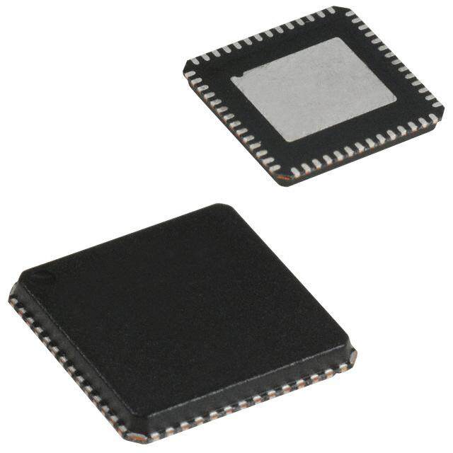
| 封装/箱体 | QFN-64 |
| 工作电源电压 | 1.25 V, 3.3 V |
| 工厂包装数量 | 260 |
| 接口类型 | SPI, USB |
| 数据速率 | 5 Gbps, 480 Mbps, 12 Mbps, 1.5 Mbps |
| 最大工作温度 | + 70 C |
| 最小工作温度 | 0 C |
| 标准 | USB 3.0 |
| 标准包装 | 260 |
| 端口数量 | 4 Port |
| 类型 | Hub Controller |
| 速度 | SuperSpeed |


- 商务部:美国ITC正式对集成电路等产品启动337调查
- 曝三星4nm工艺存在良率问题 高通将骁龙8 Gen1或转产台积电
- 太阳诱电将投资9.5亿元在常州建新厂生产MLCC 预计2023年完工
- 英特尔发布欧洲新工厂建设计划 深化IDM 2.0 战略
- 台积电先进制程称霸业界 有大客户加持明年业绩稳了
- 达到5530亿美元!SIA预计今年全球半导体销售额将创下新高
- 英特尔拟将自动驾驶子公司Mobileye上市 估值或超500亿美元
- 三星加码芯片和SET,合并消费电子和移动部门,撤换高东真等 CEO
- 三星电子宣布重大人事变动 还合并消费电子和移动部门
- 海关总署:前11个月进口集成电路产品价值2.52万亿元 增长14.8%


PDF Datasheet 数据手册内容提取
USB5534B 4-Port SS/HS USB Hub Controller General Description • Emulates portable/handheld native wall chargers - Charging profiles emulate a handheld The USB5534B hub is a 4-port SuperSpeed/Hi-Speed, device’s wall charger to enable fast charging low-power, configurable hub controller family fully com- (minutes vs. hours) pliant with the USB 3.0 Specification. The USB5534B • Enables charging from a mobile platform that is supports 5Gbps SuperSpeed (SS), 480Mbps Hi- off Speed (HS), 12Mbps Full-Speed (FS) and 1.5Mbps Low-Speed (LS) USB signaling for complete coverage • Support tablets’ high current requirements of all defined USB operating speeds. • Optimized for low-power operation and low ther- mal dissipation The USB5534B supports USB 2.0 speeds through its USB 2.0 hub controller. The new SuperSpeed hub con- • Vendor Specific Messaging (VSM) support for troller operates in parallel with the USB 2.0 controller, firmware upload over USB so the 5Gbps SuperSpeed data transfers are not • Configuration via OTP ROM, SPI ROM, or SMBus affected by the slower USB 2.0 traffic. • Intelligent charge management with UCS1002 The USB5534B supports battery charging on a per port control basis. On battery charging enabled ports, the devices • On-chip 8051µC manages VBUS, and other hub provide automatic USB data line handshaking. The signals handshaking supports USB 1.2 Charging Downstream • 8KB RAM, 32KB ROM Port (CDP), Dedicated Charging Port (DCP) and non- • One Time programmable (OTP) ROM: 8kbit USB 1.2 devices. - Includes on-chip charge pump The USB5534B is configured for operation through • Single 25MHz XTAL or clock input for all on-chip internal default settings, where custom configurations PLL and clocking requirements are supported through an on-chip OTP ROM, an exter- • Supports JTAG boundary scan nal SPI ROM, or SMBus. • PHYBoost (USB 2.0) Product Features - Selectable drive strength for improved signal integrity • USB 3.0 compliant 5Gbps, 480Mbps, 12Mbps • VariSense (USB 2.0) and 1.5Mbps operation, USB pins are 5V toler- - controls the receiver sensitivity enabling four ant programmable levels of USB signal receive - Integrated termination and pull-up/pull-down sensitivity resistors • IETF RFC 4122 compliant 128-bit UUID • Four downstream USB 3.0 ports • Supports battery charging of most popular battery Software Features powered devices • Compatible with Microsoft Windows 7, Vista, XP, - USB-IF Battery Charging rev. 1.2 support MacOSX10.4+, and Linux Hub Drivers (DCP & CDP) - Apple Portable product charger emulation - Blackberry charger emulation - Chinese YD/T 1591-2006 charger emulation - Chinese YD/T 1591-2009 charger emulation - Supports additional portable devices 2012 - 2015 Microchip Technology Inc. DS00001681C-page 1
USB5534B TO OUR VALUED CUSTOMERS It is our intention to provide our valued customers with the best documentation possible to ensure successful use of your Microchip products. To this end, we will continue to improve our publications to better suit your needs. Our publications will be refined and enhanced as new volumes and updates are introduced. If you have any questions or comments regarding this publication, please contact the Marketing Communications Department via E-mail at docerrors@microchip.com. We welcome your feedback. Most Current Data Sheet To obtain the most up-to-date version of this data sheet, please register at our Worldwide Web site at: http://www.microchip.com You can determine the version of a data sheet by examining its literature number found on the bottom outside corner of any page. The last character of the literature number is the version number, (e.g., DS30000000A is version A of document DS30000000). Errata An errata sheet, describing minor operational differences from the data sheet and recommended workarounds, may exist for cur- rent devices. As device/documentation issues become known to us, we will publish an errata sheet. The errata will specify the revision of silicon and revision of document to which it applies. To determine if an errata sheet exists for a particular device, please check with one of the following: • Microchip’s Worldwide Web site; http://www.microchip.com • Your local Microchip sales office (see last page) When contacting a sales office, please specify which device, revision of silicon and data sheet (include -literature number) you are using. Customer Notification System Register on our web site at www.microchip.com to receive the most current information on all of our products. DS00001681C-page 2 2012 - 2015 Microchip Technology Inc.
USB5534B Table of Contents 1.0 Introduction .....................................................................................................................................................................................4 2.0 Block Diagram .................................................................................................................................................................................6 3.0 Pin Information ................................................................................................................................................................................7 4.0 Standard Interface Connections ...................................................................................................................................................13 5.0 Functional Operation .....................................................................................................................................................................24 6.0 DC Parameters .............................................................................................................................................................................57 7.0 AC Specifications ..........................................................................................................................................................................61 8.0 Package Drawing ..........................................................................................................................................................................64 Appendix A: Data Sheet Revision History ...........................................................................................................................................66 Appendix B: Acronyms ........................................................................................................................................................................68 Appendix C: References .....................................................................................................................................................................69 The Microchip Web Site ......................................................................................................................................................................70 Customer Change Notification Service ...............................................................................................................................................70 Customer Support ...............................................................................................................................................................................70 Product Identification System .............................................................................................................................................................71 2012 - 2015 Microchip Technology Inc. DS00001681C-page 3
USB5534B 1.0 INTRODUCTION 1.1 Conventions Within this manual, the following abbreviations and symbols are used to improve readability. Example Description BIT Name of a single bit within a field FIELD.BIT Name of a single bit (BIT) in FIELD x…y Range from x to y, inclusive BITS[m:n] Groups of bits from m to n, inclusive PIN Pin Name zzzzb Binary number (value zzzz) 0xzzz Hexadecimal number (value zzz) zzh Hexadecimal number (value zz) rsvd Reserved memory location. Must write 0, read value indeterminate code Instruction code, or API function or parameter Used for multiple words that are considered a single unit, such as: Multi Word Name Resource Allocate message, or Connection Label, or Decrement Stack Pointer instruction. Section Name Section or Document name. x Don’t care <Parameter> <> indicate a Parameter is optional or is only used under some conditions {,Parameter} Braces indicate Parameter(s) that repeat one or more times. Brackets indicate a nested Parameter. This Parameter is not real and actually decodes into [Parameter] one or more real parameters. 1.2 Overview The USB5534B hub is a 4-port, low-power, configurable Hub Controller fully compliant with the USB 3.0 Specification 2. The USB5534B supports 5Gbps SuperSpeed (SS), 480Mbps Hi-Speed (HS), 12Mbps Full-Speed (FS) and 1.5Mbps Low-Speed (LS) USB signaling for complete coverage of all defined USB operating speeds. All required resistors on the USB ports are integrated into the hub. This includes all series termination resistors and all required pull-down and pull-up resistors on D+ and D- pins. The over-current sense inputs for the downstream facing ports have internal pull-up resistors. The USB5534B hub includes programmable features such as: • MultiTRAKTM Technology (USB 2.0): implements a dedicated Transaction Translator (TT) for each port. Dedi- cated TTs help maintain consistent full-speed data throughput regardless of the number of active downstream connections. • PortSwap (USB 2.0): allows direct alignment of USB signals (D+/D-) to connectors to avoid uneven trace length or crossing of the USB differential signals on the PCB. • PHYBoost (USB 2.0): enables 4 programmable levels of USB signal drive strength in downstream port transceiv- ers. PHYBoost will also attempt to restore USB signal integrity. As shown on the Product Identification System page, two USB5534B firmware versions are available: “-5000” and “- 6080”. These options differ in the following ways: • The Dynamic Charging Port feature and related DYNCPDIS_N pin function are only available on the -6080 device. Refer to Section 5.1.3, "Dynamic Charging Port (6080 Only)" for additional details. • The TRST/DYNCPDIS_N/UCS_SMBALERT_N pin buffer type is “IPU” in the -6080 device and “I” in the -5000 device. Refer to Pin Information on page 7 for additional details. • The Global Suspend power consumption has been significantly lowered in the -6080 device. Refer to Section 6.3, "Power Consumption" for additional details. DS00001681C-page 4 2012 - 2015 Microchip Technology Inc.
USB5534B 1.3 Configurable Features The USB5534B hub controller provides a default configuration that is sufficient for most applications. When initialized in the default configuration, the following features may be configured: • Downstream non-removable ports, where the hub will automatically report as a compound device • Downstream disabled ports • Downstream port power control and over-current detection on a ganged or individual basis • USB signal drive strength • USB differential pair pin location The USB5534B hub controllers can alternatively be configured by OTP or as an SMBus slave device. When configured by an OTP or over SMBus, the following configurable features are provided: • Support for compound devices on a port-by-port basis • Selectable over-current sensing and port power control on an individual or ganged basis to match the circuit board component selection • Customizable vendor ID, product ID, and device ID • Configurable delay time for filtering the over-current sense inputs • Indication of the maximum current that the hub consumes from the USB upstream port • Indication of the maximum current required for the hub controller • Custom string descriptors (up to 30 characters): Product, manufacturer, and serial number 2012 - 2015 Microchip Technology Inc. DS00001681C-page 5
USB5534B 2.0 BLOCK DIAGRAM FIGURE 2-1: USB5534B BLOCK DIAGRAM PI S 0 4 B2.HY ort SP P U B S SPI Master Timer Buffer RX SSPHY stream U Buffer TX SSPHY Down Upstream USB Port XDataTXRXXData to USB2.0EmbeddedAPB BridgeSSSSPHY8051 µCReset & 8051 PHYPHYBoot Seq.32k ROMBufferBuffer8k RAM2k OTP APB Bus Registers Registers & Hub I/O& Hub I/O USB 3.0 Hub ControllerUSB 2.0 Hub Controller VBUSControl HS/FS/LS Routing Logic Downstream TX SS bus Downstream RX SS bus BufferBufferBufferBuffer TXRXTXRXUSB2.0USB2.0SSSSSSSSPHYPHYPHYPHYPHYPHY Downstream USB Port 2Downstream USB Port 3 mmon ockPLL USB2.0PHY B Port 1 CoBl& Buffer RX SSPHY eam US str Buffer TX SSPHY Down DS00001681C-page 6 2012 - 2015 Microchip Technology Inc.
USB5534B 3.0 PIN INFORMATION This chapter outlines the pinning configurations for each chip. The detailed pin descriptions are listed by function in Sec- tion 3.2, "Pin Descriptions (Grouped by Function)," on page8. 3.1 Pin Configurations FIGURE 3-1: USB5534B 64-PIN QFN 1 2 3 L L L N/N T T T __ C C C ST _ _ _ BUS MS/OCS2 CK/OCS1 RST/DYNCPDICS_SMBALER DI/OCS3 DO/OCS4 PI_DI PI_DO PI_CLK PI_CE_N M_CLK M_DAT RT_PWR1/PRT RT_PWR2/PRT DD33 RT_PWR3/PRT V T T TU T T S S S S S S P P V P 48 47 46 45 44 43 42 41 40 39 38 37 36 35 34 33 TEST 49 32 PRT_PWR4/PRT_CTL4 RESET_N 50 31 VDD12 VDD12 51 30 USB3DM_RXDN4 VDD33 52 29 USB3DP_RXDN4 USB2DP_UP 53 28 VDD12 USB2DM_UP 54 27 USB3DM_TXDN4 USB3DP_TXUP 55 26 USB3DP_TXDN4 USB3DM_TXUP 56 25 USB2DM_DN4 USB5534B VDD12 57 24 USB2DP_DN4 (Top View QFN-64) USB3DP_RXUP 58 23 USB3DM_RXDN3 USB3DM_RXUP 59 22 USB3DP_RXDN3 ATEST 60 21 VDD12 XTALOUT 61 20 USB3DM_TXDN3 Ground Pad XTALIN/CLK_IN 62 19 USB3DP_TXDN3 (must be connected to VSS with a via field) VDD33 63 18 USB2DM_DN3 RBIAS 64 17 USB2DP_DN3 1 2 3 4 5 6 7 8 9 10 11 12 13 14 15 16 1 1 1 1 2 1 1 2 2 2 2 2 2 2 2 3 N N N N 1 N N 1 N N N N 1 N N 3 D D D D D D D D D D D D D D D D _ _ X X D X X D _ _ X X D X X D USB2DP USB2DM USB3DP_T USB3DM_T V USB3DP_R USB3DM_R V USB2DP USB2DM USB3DP_T USB3DM_T V USB3DP_R USB3DM_R V Indicates pins on the bottom of the device. 2012 - 2015 Microchip Technology Inc. DS00001681C-page 7
USB5534B 3.2 Pin Descriptions (Grouped by Function) An N at the end of a signal name indicates that the active (asserted) state occurs when the signal is at a low voltage level. When the N is not present, the signal is asserted when it is at a high voltage level. The terms assertion and nega- tion are used exclusively in order to avoid confusion when working with a mixture of active low and active high signals. The term assert, or assertion, indicates that a signal is active, independent of whether that level is represented by a high or low voltage. The term negate, or negation, indicates that a signal is inactive. TABLE 3-1: USB5534B PIN DESCRIPTIONS Symbol Buffer Type Description USB 3.0 INTERFACE USB3DP_TXUP IO-U USB 3 Upstream Upstream SuperSpeed transmit data plus USB3DM_TXUP IO-U USB 3 Upstream Upstream SuperSpeed transmit data minus USB3DP_RXUP IO-U USB 3 Upstream Upstream SuperSpeed receive data plus USB3DM_RXUP IO-U USB 3 Upstream Upstream SuperSpeed receive data minus USB3DP_TXDN[4:1] IO-U USB 3 Downstream Downstream SuperSpeed transmit data plus for ports 1 through 4. USB3DM_TXDN[4:1] IO-U USB 3 Downstream Downstream SuperSpeed transmit data minus for ports 1 through 4. USB3DP_RXDN[4:1] IO-U USB 3 Downstream Downstream SuperSpeed receive data plus for ports 1 through 4. USB3DM_RXDN[4:1] IO-U USB 3 Downstream Downstream SuperSpeed receive data minus for ports 1 through 4. USB 2.0 INTERFACE USB2DP_UP IO-U USB Bus Data These pins connect to the upstream USB bus data signals. USB2DM_UP IO-U USB Bus Data These pins connect to the upstream USB bus data signals. USB2DP_DN[4:1] USB Downstream IO-U Downstream Hi-Speed data plus for ports 1 through 4. USB2DM_DN[4:1] USB Downstream IO-U Downstream Hi-Speed data minus for ports 1 through 4. DS00001681C-page 8 2012 - 2015 Microchip Technology Inc.
USB5534B TABLE 3-1: USB5534B PIN DESCRIPTIONS (CONTINUED) Symbol Buffer Type Description USB PORT CONTROL PRT_PWR[4:1]/ O12 USB Power Enable PRT_CTL[4:1] Enables power to USB peripheral devices downstream. Note: This pin also provides configuration strap functions. See Note 3-1. VBUS I Upstream VBUS Power Detect This pin can be used to detect the state of the upstream bus power. The device monitors this pin to determine when to assert the internal D+ pull- up resistor (signaling a connect event). When designing a detachable hub, this pin should be connected to VBUS on the upstream port via a 2:1 voltage divider. Two 100 k resistors are suggested. For self-powered applications with a permanently attached host, this pin must be connected to a dedicated host control output, or connected to the 3.3 V domain that powers the host (typically VDD33). SPI INTERFACE (4 PINS) SPI_CE_N O12 SPI Enable SPI_CLK O12 SPI Clock SPI_DO SPI Serial Data Out The output for the SPI port. O12 Note: This pin also provides configuration strap functions. See . SPI_DI I SPI Serial Data In The SPI data in to the controller from the ROM. This pin has a weak internal pull-down applied at all times to prevent floating. JTAG/OCS INTERFACE TRST JTAG Asynchronous Reset Note: If using the SMBus interface, a pull-up on this signal will enable Legacy Mode, while leaving it unconnected or pulled-down will enable Advanced Mode. Note: Only available in test mode. DYNCPDIS_N IPU Dynamic Charging Port Disable (Note 3-4) This active-low signal is used to globally disable Battery Charging support on all USB downstream ports configured as Charging Ports. Note: This signal available in -6080 versions only UCS_SMBALERT_N UCS1002 SMBus Alert When charging port is enabled and SMBus devices are used, this signal acts as an active-low SMBus alert. 2012 - 2015 Microchip Technology Inc. DS00001681C-page 9
USB5534B TABLE 3-1: USB5534B PIN DESCRIPTIONS (CONTINUED) Symbol Buffer Type Description TCK JTAG Clock This input is used for JTAG boundary scan and has a weak pull-down. It can be left floating or grounded when not used. If the JTAG is connected, then this signal will be detected high, and the software disables the pull up after reset. I Note: Only available in test mode. OCS1 Over-Current Sense 1 Input from external current monitor indicating an over-current condition. Note: This pin also provides configuration strap functions. See Note 3-3. TMS JTAG TMS Used for JTAG boundary scan. Note: Only available in test mode. OCS2 I Over-Current Sense 2 Input from external current monitor indicating an over-current condition. Note: This pin also provides configuration strap functions. See Note 3-3. TDI JTAG TDI Used for JTAG boundary scan. Note: Only available in test mode. OCS3 I Over-Current Sense 3 Input from external current monitor indicating an over-current condition. Note: This pin also provides configuration strap functions. See Note 3-3. TDO JTAG TDO Used for JTAG boundary scan. Note: Only available in test mode. OCS4 O12 Over-Current Sense 4 Input from external current monitor indicating an over-current condition. Note: This pin also provides configuration strap functions. See Note 3-3. MISC RESET_N IS Reset Input The system uses this active low signal to reset the chip. The active low pulse should be at least 1s wide. XTALIN Crystal Input: 25MHz crystal. This pin connects to either one terminal of the crystal or to an external 25MHz clock when a crystal is not used. ICLKx CLK_IN External Clock Input This pin connects to either one terminal of the crystal or to an external 25MHz clock when a crystal is not used. XTALOUT OCLKx Crystal Output The clock output, providing a crystal 25MHz. When an external clock source is used to drive XTALIN/CLK_IN, this pin becomes a no connect. DS00001681C-page 10 2012 - 2015 Microchip Technology Inc.
USB5534B TABLE 3-1: USB5534B PIN DESCRIPTIONS (CONTINUED) Symbol Buffer Type Description TEST IPD Test Pin Treat as a no connect pin or connect to ground. No trace or signal should be routed or attached to this pin. RBIAS I-R USB Transceiver Bias A12.0k (+/- 1%) resistor is attached from ground to this pin to set the transceiver’s internal bias settings. ATEST A Analog Test Pin This signal is used for testing the chip and must always be connected to ground. SM_CLK I/O12 SMBus Clock SM_DAT I/O12 SMBus Data Pin DIGITAL AND POWER (4) VDD33 3.3V Power (8) VDD12 1.25V Power VSS Ground Pad This exposed pad is the device’s only connection to VSS and the primary thermal conduction path. Connect to an appropriate via field. Note 3-1 The PRT_PWR[4:1] pins can optionally provide additional configuration strap functions to enable/disable the associated port and configure its battery charging capabilities. Configuration strap values are latched on device reset. Table3-2 details the functions associated with the various strap settings. Strapping features are enabled by default and can be optionally disabled via the Pro-Touch software programming tool. For additional information on the Pro-Touch programming tool, contact your local sales representative. Strapping functions are not supported for designs that support OCS but not power switching. TABLE 3-2: PRT_PWR[4:1] CONFIGURATION STRAP STATES PRT_PWR[4:1] Port State Battery Charging Strap Setting No Pull-Up or Pull-Down Enabled Disabled Pull-Down: Disabled N/A <10kto VSS Pull-Up: Enabled Enabled <10kand >1k to VDD33 Note 3-2 The SPI_DO pin provides an additional SPI_SPD_SEL configuration strap function. SPI_SPD_SEL selects between the 30MHz SPI Mode when pulled-down to ground (default) and the 60MHz SPI Mode when pulled-up to VDD33. The SPI_SPD_SEL strap value is latched on Power-On Reset (POR) or RESET_N deassertion. Note 3-3 The OCS[4:1] pins can optionally provide additional configuration strap functions. To set the associated port into the non-removable state, the OCS pin must be configured with a pull-down (<10kto VSS). Otherwise, the port will be configured in the removable state. Configuration strap values are latched on device reset. Strapping features are enabled by default and can be optionally disabled via the Pro-Touch software programming tool. For additional information on the Pro-Touch programming tool, contact your local sales representative. Strapping functions are not supported for designs that support OCS but not power switching. 2012 - 2015 Microchip Technology Inc. DS00001681C-page 11
USB5534B Note 3-4 This pin has an internal pull-up only in the -6080 version. The internal pull-up is only active after the SMBus mode (Legacy/Advanced) configuration strap has been sampled at POR or reset. The -5000 version is an “I” type buffer. 3.3 Buffer Type Descriptions TABLE 3-3: BUFFER TYPE DESCRIPTIONS Buffer Type Description I Input I/O Input/output IPD Input with internal weak pull-down resistor IPU Input with internal weak pull-up resistor IS Input with Schmitt trigger O12 Output 12mA I/O12 Input/output buffer with 12mA sink and 12mA source I/OSD12 Open drain with Schmitt trigger and 12mA sink. ICLKx XTAL clock input OCLKx XTAL clock output I-R RBIAS I/O-U Analog input/output defined in USB specification DS00001681C-page 12 2012 - 2015 Microchip Technology Inc.
USB5534B 4.0 STANDARD INTERFACE CONNECTIONS 4.1 SPI Interface The hub will interface to external memory depending on configuration of the USB5534B pins associated with each inter- face type. The USB5534B will first check to see whether an external SPI Flash is present. If not, the USB5534B will operate from internal ROM. If SPI Flash is present, the chip will operate from the external ROM. The USB5534B is capable of code execution from an external SPI ROM. On power up, the firmware looks for an external SPI flash device that contains a valid signature of 2DFU (device firmware upgrade) beginning at address 0xFFFA. If a valid signature is found, then the external ROM is enabled and the code execution begins at address 0x0000 in the external SPI device. If a valid signature is not found, then execution continues from internal ROM. The following sections describe the interface options to the external SPI ROM. 4.1.1 OPERATION OF THE HI-SPEED READ SEQUENCE The SPI controller will automatically handle code reads going out to the SPI ROM Address. When the controller detects a read, the controller drops the SPI_CE, and puts out a 0x0B, followed by the 24-bit address. The SPI controller then puts out a DUMMY byte. The next eight clocks clock in the first byte. When the first byte is clocked in a ready signal is sent back to the processor, and the processor gets one byte. After the processor gets the first byte, its address will change. If the address is one more than the last address, the SPI controller will clock out one more byte. If the address in anything other than one more than the last address, the SPI controller will terminate the transaction by taking SPI_CE high. As long as the addresses are sequential, the SPI Con- troller will keep clocking in data. FIGURE 4-1: SPI HI-SPEED READ OPERATION USB Hub CE# ADDRESS SPI CONTROL CONTROLLER CLK SI SPI CACHE ROM SPI_DI Serial to SO Parllel 2012 - 2015 Microchip Technology Inc. DS00001681C-page 13
USB5534B FIGURE 4-2: SPI HI-SPEED READ SEQUENCE SPI_CEN 0 1 2 3 4 5 6 7 8 1516 2324 3132 3940 4748 5556 6364 7172 80 SPI_CLK SPI_DO 0B ADD. ADD. ADD. X MSB MSB N N+1 N+2 N+3 N+4 SPI_DI HIGH IMPEDANCE DOUT DOUT DOUT DOUT DOUT MSB 4.1.2 OPERATION OF THE DUAL HI-SPEED READ SEQUENCE The SPI controller also supports dual data mode (at 30 MHz SPI speed only). When configured in dual mode, the SPI controller will automatically handle reads going out to the SPI ROM. When the controller detects a read, the controller drops the SPI_CE_N, and puts out a 0x3B, followed by the 24-bit address. The SPI controller then puts out a DUMMY byte. The next four clocks clock in the first byte. The data appears two bits at a time on data out and data in. When the first byte is clocked in a ready signal is sent back to the processor, and the processor gets one byte. After the processor gets the first byte, the address will change. If the address is one more than the last address, the SPI controller will clock out one more byte. If the address in anything other than one more than the last address, the SPI controller will terminate the transaction by taking SPI_CE_N high. As long as the addresses are sequential, the SPI Con- troller will keep clocking in data. FIGURE 4-3: SPI DUAL HI-SPEED READ OPERATION USB Hub CE# ADDRESS SPI CONTROL CONTROLLER CLK SPI CACHE SI ROM SPI_DI 2-Serial to 8-Parallel SO DS00001681C-page 14 2012 - 2015 Microchip Technology Inc.
USB5534B FIGURE 4-4: SPI DUAL HI-SPEED READ SEQUENCE SPI_CEN 0 1 2 3 4 5 6 7 8 1516 2324 3132 3940 4344 4748 5152 5556 59 SPI_CLK N N+1 N+2 N+3 N+4 D1 D2 D3 D4 D5 SPI_DO 0B ADD. ADD. ADD. X Bits-6,4,2,0 Bits-6,4,2,0 Bits-6,4,2,0 Bits-6,4,2,0 Bits-6,4,2,0 MSB MSB MSB N N+1 N+2 N+3 N+4 SPI_DI HIGH IMPEDANCE D1 D2 D3 D4 D5 Bits-7,5,3,1 Bits-7,5,3,1 Bits-7,5,3,1 Bits-7,5,3,1 Bits-7,5,3,1 MSB 4.1.3 32-BYTE CACHE There is a 32-byte pipeline cache, and associated with the cache is a base address pointer and a length pointer. Once the SPI controller detects a jump, the base address pointer is initialized to that address. As each new sequential data byte is fetched, the data is written into the cache, and the length is incremented. If the sequential run exceeds 32 bytes, the base address pointer is incremented to indicate the last 32 bytes fetched. If the USB5534B does a jump, and the jump is in the cache address range, the fetch is done in 1 clock from the internal cache instead of an external access. 4.1.4 INTERFACE OPERATION TO SPI PORT WHEN NOT DOING FAST READS There is an 8-byte command buffer: SPI_CMD_BUF[7:0]; an 8-byte response buffer: SPI_RESP_BUF[7:0]; and a length register that counts out the number of bytes: SPI_CMD_LEN. Additionally, there is a self-clearing GO bit in the SPI_CTL Register. Once the GO bit is set, the device drops SPI_CE_N, and starts clocking. It will put out SPI_CMD_LEN X 8 num- ber of clocks. After the first byte, the COMMAND, has been sent out, and the SPI_DI is stored in the SPI_RESP buffer. If the SPI_CMD_LEN is longer than the SPI_CMD_BUF, don’t cares are sent out on the SPI_DO line. This mode is used for program execution out of internal RAM or ROM. FIGURE 4-5: SPI INTERNALLY-CONTROLLED OPERATION USB Hub CE# SPI SPI_CMD_LEN CONTROLLER CLK SPI_CMD_BUF[3:0] SI SPI ROM SPI_RSP_BUF[7:0] SO 2012 - 2015 Microchip Technology Inc. DS00001681C-page 15
USB5534B 4.1.4.1 ERASE EXAMPLE To perform a SCTR_ERASE, 32BLK_ERASE, or 64BLK_ERASE, the device writes 0x20, 0x52, or 0xD8, respectively to the first byte of the command buffer, followed by a 3-byte address. The length of the transfer is set to 4 bytes. To do this, the device first drops SPI_CE_N, then counts out 8 clocks. It then puts out the 8 bits of command, followed by 24 bits of address of the location to be erased on the SPI_DO pin. When the transfer is complete, the SPI_CE_N goes high, while the SPI_DI line is ignored in this example. FIGURE 4-6: SPI ERASE SEQUENCE SPI_CEN 0 1 2 3 4 5 6 7 8 1516 2324 31 SPI_CLK Command ADD. ADD. ADD. SPI_DO MSB MSB SPI_DI HIGH IMPEDANCE 4.1.4.2 BYTE PROGRAM EXAMPLE To perform a Byte Program, the device writes 0x02 to the first byte of the command buffer, followed by a 3-byte address of the location that will be written to, and one data byte. The length of the transfer is set to 5 bytes. The device first drops SPI_CE_N, 8 bits of command are clocked out, followed by 24 bits of address, and one byte of data on the SPI_DO pin. The SPI_DI line is not used in this example. FIGURE 4-7: SPI BYTE PROGRAM SPI_CEN 0 1 2 3 4 5 6 7 8 1516 2324 3132 39 SPI_CLK SPI_DO 0xDB 0x00 0xBF /00xxFFEF Data MSB MSB MSB LSB SPI_DI HIGH IMPEDANCE DS00001681C-page 16 2012 - 2015 Microchip Technology Inc.
USB5534B 4.1.4.3 COMMAND ONLY PROGRAM EXAMPLE To perform a single byte command such as the following: - - WRDI - - WREN - - EWSR - - CHIP_ERASE - - EBSY - - DBSY The device writes the opcode into the first byte of the SPI_CMD_BUF and the SPI_CMD_LEN is set to one. The device first drops SPI_CE, then 8 bits of the command are clocked out on the SPI_DO pin. The SPI_DI is not used in this exam- ple. FIGURE 4-8: SPI COMMAND ONLY SEQUENCE SPI_CEN 0 1 2 3 4 5 6 7 SPI_CLK Command SPI_DO MSB SPI_DI HIGH IMPEDANCE 4.1.4.4 JEDEC-ID READ EXAMPLE To perform a JEDEC-ID command, the device writes 0x9F into the first byte of the SPI_CMD_BUF and the length of the transfer is 4 bytes. The device first drops SPI_CE_N, then 8 bits of the command are clocked out, followed by the 24 bits of dummy bytes (due to the length being set to 4) on the SPI_DO pin. When the transfer is complete, the SPI_CE_N goes high. After the first byte, the data on SPI_DI is clocked into the SPI_RSP_BUF. At the end of the command, there are three valid bytes in the SPI_RSP_BUF. In this example, 0xBF, 0x25, 0x8E. 2012 - 2015 Microchip Technology Inc. DS00001681C-page 17
USB5534B FIGURE 4-9: SPI JEDEC-ID SEQUENCE SPI_CEN 0 1 2 3 4 5 6 7 8 910111213141516171819202122232425262728293031323334 SPI_CLK 9F SPI_DO MSB SPI_DI HIGH IMPEDANCE BF 25 8E MSB MSB 4.2 SMBus Slave Interface Next, the USB5534B will look to receive configuration and commands from an optional SMBus master (if present). When SMBus is enabled, the SMBus can operate in either legacy (USB 2.0 only) or advanced mode (access to both USB 2.0 and 3.0 registers). Next, the USB5534B will look for (optional) configuration present in the internal OTP memory. Any register settings that are modified via the SMBus interface will overwrite the internal OTP settings. The SMBus slave interface is enabled when pull-up resistors are detected on both SM_DAT and SM_CLK for the first millisecond after reset. For operation in SMBus Legacy Mode, an additional pull-up resistor is required on TRST. If the SMBus interface is enabled, then the USB5534B will wait indefinitely for the SMBus host to configure the device. Once SMBus configuration is complete, device initialization will proceed. To disable the SMBus, a pull-down resistor of 10K must be applied to either SM_DAT, SM_CLK, or both SM_DAT and SM_CLK if desired. If SMBus is disabled, the device proceeds directly to device initialization using the internal OTP ROM. 4.2.1 PULL-UP RESISTOR FOR SMBUS External pull-up resistors (10k recommended) are required on the SM_DAT and SM_CLK pins when implementing either SMBus mode. DS00001681C-page 18 2012 - 2015 Microchip Technology Inc.
USB5534B FIGURE 4-10: SMBUS SLAVE CONNECTION VDD USB Hub 10 k 10 k SCL SM_CLK SDA SM_DAT Master 4.2.1.1 Invalid Protocol Response Behavior Note that any attempt to update registers with an invalid protocol will not be updated. The only valid protocols are write block and read block (described Section 5.5, "SMBus Slave Interface," on page29), where the hub only responds to the 7-bit hardware selected slave addresses (0101100b or 0101101b). Additionally, the only valid registers for the hub are outlined in the USB5534B Configuration Release Notes documentation. 4.2.2 SLAVE DEVICE TIMEOUT Devices in a transfer can abort the transfer in progress and release the bus when any single clock low interval exceeds 25ms (T ). The master must detect this condition and generate a stop condition within or after the transfer TIMEOUT, MIN of the interrupted data byte. Slave devices must reset their communication and be able to receive a new START condi- tion no later than 35ms (T ). TIMEOUT, MAX Note: Some simple devices do not contain a clock low drive circuit; this simple kind of device typically resets its communications port after a start or stop condition. The slave device timeout must be implemented. 4.2.3 STRETCHING THE SCLK SIGNAL The hub supports stretching of the SCLK by other devices on the SMBus. The hub will stretch the clock as needed. 4.2.4 BUS RESET SEQUENCE The SMBus slave interface resets and returns to the idle state upon a START condition followed immediately by a STOP condition. 4.2.5 SMBUS ALERT RESPONSE ADDRESS The SMBALERT# signal is not supported by the USB5534B. 2012 - 2015 Microchip Technology Inc. DS00001681C-page 19
USB5534B 4.3 Reset There are two different resets that the device experiences. One is a hardware reset (either from the internal POR reset circuit or via the RESET_N pin) and the second is a USB Bus Reset. 4.3.1 INTERNAL POR All reset timing parameters are guaranteed by design. 4.3.2 EXTERNAL HARDWARE RESET A valid hardware reset is defined as assertion of RESET_N for a minimum of 1s after all power supplies are within operating range. Assertion of RESET_N (external pin) causes the following: 1. The PHY is disabled, and the differential pairs will be in a high-impedance state. 2. All transactions immediately terminate; no states are saved. 3. All internal registers return to the default state. 4. The external crystal oscillator is halted. 5. The PLL is halted. 4.4 Standard Port Power Configuration The device natively operates with standard port power controllers or poly-fuse devices for the downstream port powers when battery charging is not enabled on a port. It is not recommended to have the downstream ports of a single device mix poly-fuse and standard power controller support, as the configuration of the hub cannot correctly report which ports are poly-fuse and which are port power controllers to the host. Any port without battery charging can also be used in individual port power controls or ganged power controls. The port power control output only supports either Ganged or Individual modes on a global basis for all downstream ports. The overcurrent setting also supports individual or global settings, but also adds the ability to configure specific ports to be part of an overcurrent gang with others setup for individual connections. This hybrid configuration should only be used when utilizing poly-fuse power devices. 4.4.1 PORT POWER CONTROLLER The most common method for downstream port power controls is to utilize current-limited power switches for USB appli- cations. The devices allow the downstream port powers to be enabled through a control signal and report over-current conditions through a flag output. Two connection methods are possible for these controllers, Combined mode and Independent mode. In Combined mode, the FLG and EN signals are tied together with an external 10K ohm pull-up and driven to a single PRT_CTL signal on the device, as shown in Figure4-11. DS00001681C-page 20 2012 - 2015 Microchip Technology Inc.
USB5534B FIGURE 4-11: COMBINED MODE IMPLEMENTATION 5V PRT_CTL OCS USB Power USB553x Switch EN USB Device In Individual mode, the PRT_CTL signal is driven directly to the EN input of the power switch and the OCS input is con- nected to the FLG output of the power switch with a 10K pull-up connected, as shown in Figure4-12. FIGURE 4-12: INDIVIDUAL MODE IMPLEMENTATION 5V PRT_CTL EN 5V USB Power USB553x Switch 10k OCS FLG USB Device 2012 - 2015 Microchip Technology Inc. DS00001681C-page 21
USB5534B 4.4.2 POLY-FUSE An alternate method of downstream power control is to utilize poly-fuse devices. In this configuration, the poly-fuse devices are used to report overcurrent conditions to the USB5534B through the OCS input, as shown in Figure4-13. FIGURE 4-13: POLY-FUSE IMPLEMENTATION 5V 3.3V Poly Fuse 10k OCS USB553x USB Device 4.5 Charging Port Configurations The device can also be configured to operate as a charging port for one or more downstream ports. Ganged port power control and/or overcurrent is not supported if any of the downstream ports are configured as charging ports. If a port is configured to support a charging port mode, either a standard port power controller or a UCS1002 may be implemented. For more information on charging port support, refer to Section 5.1, "Charging Port Configuration," on page24. 4.5.1 PORT POWER CONTROLLER The only special limitation of using the device as a charging port is that the port power controller must be capable of the higher current to support the charging port modes. Refer to Section 4.4.1, "Port Power Controller," on page20 for more information on this implementation. 4.5.2 UCS1002 Using a UCS1002 device as a downstream port power controller is only supported on ports that are enabled as charging ports. If the UCS1002 is implemented, the USB5534B communicates with all of the implemented UCS1002 ports over SMBus using one of the PRT_CTLx/OCSx signals as the SMCLK/SMDAT. Additionally, DYNCPDIS_N becomes the UCS_SM- BALERT_N signal. Multiple UCS1002 devices may be connected to the SMBus in parallel. After reset, for any enabled charging ports, the USB5534B performs SMBus commands on the configured PRT_CTLx/OCSx signals and checks UCS1002 devices at specific addresses (see Table4-1) to confirm which ports are utilizing UCS1002 devices as the downstream power controllers. TABLE 4-1: UCS1002 ADDRESS MAPPING Port Address 1 0x30 2 0x31 3 0x32 4 0x33 DS00001681C-page 22 2012 - 2015 Microchip Technology Inc.
USB5534B In this configuration, the UCS1002 is utilized as an SMBus enabled port power switch and all charging port handshaking on the D+/D- signals are controlled directly from the USB5534B. An example implementation can be seen in Figure4- 14. FIGURE 4-14: UCS1002 CHARGING IMPLEMENTATION Port 1 USB 3 USB2DM_DN1 D- A-Type USB2DP_DN1 D+ Receptacle USB3DM_RXDN1 SSRX- 330 USB3DP_RXDN1 SSRX+ USB3DM_TXDN1 0.1uF SSTX- 0.1uF USB3DP_TXDN1 0.1uF SSTX+ ShL1 GND1 ShL2 GND2 ShR1 100uF Vbus ShR2 Shield 3.3V USB553x UCS1002 VBUS1 K K 0 0 1 1 VBUS2 PRT_CTL1 SMCLK/S0 TCK/OCS1 SMDATA/LATCH TRST/DYNCPDIS_N/ ALERT 5V UCS_SMBALERT_N M1 DPIN M2 10K DMIN EM_EN 33K DPOUT COMM_SEL 47K DMOUT SEL 2012 - 2015 Microchip Technology Inc. DS00001681C-page 23
USB5534B 5.0 FUNCTIONAL OPERATION This chapter details the functional operation of various device features. 5.1 Charging Port Configuration The USB5534B supports downstream charging ports on any available port. The hub contains internal hardware and algorithms to natively support various voltage levels on the D+/D- signals along with the BC 1.2 Handshaking protocol, allowing charging devices to detect the downstream port as a charging port. A port can be configured for either RapidCharge support or Samsung Legacy Charging mode support. This section details the various charging port modes. The following terminology will be helpful in the understanding of these features: • SDP - Standard Downstream Port - A port that is not operating as a charging port and has active USB communi- cations. • CDP - Charging Downstream Port - A port that is operating as a charging port and has active USB communica- tions. • DCP - Dedicated Charging Port - A port that is operating as a charging port but has no USB communications. • S0 - Normal system power state in full run. • S3 - Typically a Sleep state, where the system can be woken from USB HID devices • S4 - Typically a Hibernate sleep state, where the system state is stored to a hard drive and does not support wake from USB HID devices. • S5 - Typically an OFF state for a system. 5.1.1 RAPID CHARGE This mode enables concurrent operation of Apple, BC 1.2 and DP/DM Shorted Emulation charging. The only applicable options are to choose Apple 1A or Apple 2A charging mode on a per port basis. Refer to Section 5.2.1.1, "Apple Charging Mode," on page26. Note: Apple and DP/DM Shorted Emulation charging modes are only operational in DCP mode. 5.1.2 SAMSUNG LEGACY CHARGING This mode drives a specified voltage on the DP/DM lines to allow legacy Samsung devices to detect the port as Charging capable. This is only operational in DCP modes. 5.1.3 DYNAMIC CHARGING PORT (6080 ONLY) Dynamic Charging Port support utilizes the device’s DYNCPDIS_N pin to disable Battery Charging support globally when low and, when high, allow any ports configured as Charging Ports (either through a configuration file or straps) to resume their Battery Charging operation in the configured Charging mode. This feature is currently supported only when using standard USB port power controllers. Please contact your Microchip FAE if required to use this feature with other port power controller configurations. Figure5-1, Figure5-2, and Figure5-3 detail the operation of Dynamic Charging Port in the S0, S3, and S4/S5 power modes, respectively. For any of the flow diagram transitions, there is a Y/Z nomenclature. Y = Dynamic BC enable signal Z = Device attached and sensed by device Note: The Dynamic Charging Port feature and related DYNCPDIS_N pin function is available in the “-6080” ver- sion of the device only. DS00001681C-page 24 2012 - 2015 Microchip Technology Inc.
USB5534B FIGURE 5-1: S0 STATE TRANSITIONS S0 0/X SDP 0/0 1/1 1/0 CDP DCP 0/1 1/X FIGURE 5-2: S3 STATE TRANSITIONS S3 0/X X/X SDP Power Cycle 0/X 1/X Power Cycle X/X CDP DCP X/0 X/1 1/X FIGURE 5-3: S4/S5 STATE TRANSITIONS S4/S5 0/X X/X SDP Power Off 0/X 1/X Power On CDP Power Cycle DCP X/X X/X 1/X 2012 - 2015 Microchip Technology Inc. DS00001681C-page 25
USB5534B 5.2 Configuration Options By default, the USB5534B configuration allows the device to operate as a standard USB hub when connected to a USB host controller. The device also contains a number of configurable options which can be set through its user interfaces: • One-Time Programmable (OTP) Memory (one time burn configuration) • External SPI (only when using external SPI firmware) • SMBus Slave Interface (controlled by SMBus host controller. Must be updated every time.) Refer to Standard Interface Connections on page 13 for details on the SPI and SMBus interfaces. SPI and OTP configuration can be created and applied through the Protouch tool. The following subsections detail to various device parameters that can be configured via the Protouch tool. 5.2.1 CHARGING PORT ENABLE This option enables, on a per-port basis, DFPs to become charging ports. If this is enabled on a port, it must be config- ured as a per-port PWR/OCS control. Ganged OCS or PWR controls are not supported concurrently. The normal con- figuration is to support the RapidCharge protocol. Refer to Section 5.2.17, "Port Power/OCS Control," on page27 for more information. 5.2.1.1 Apple Charging Mode This option enables either Apple 1 Amp or Apple 2 Amp for the RapidCharge protocol charging mode when a port is configured as a charging port and not enabled for Samsung Mode. This mode enables the selected Apple charging mode to operate concurrently with BC1.2. 5.2.1.2 Samsung Charging Mode This option enables the Samsung Charging mode on a port. If this is selected, the Apple Charging mode setting is ignored and only the Samsung charging mode is supported on that port. 5.2.1.3 UCS1002 SMBus Interface Selection USC1002 port power controllers are only supported if battery charging is enabled on that port. When BC is enabled, there is an option to select the external signals (PRTCTLx/OCSx) that are used for the SMBus SDA/SCL signals. Only Ports 1-4 signals can be used. This feature is supported on the “-6080” and newer devices. 5.2.2 USB VID This field is the 16-bit USB Vendor ID reported by both USB 2.0 and USB 3.0 hubs. 5.2.3 USB2 PID This field is the 16-bit USB Product ID reported by the USB 2.0 hub only. 5.2.4 USB3 PID This field is the 16-bit USB Product ID reported by the USB 3.0 Hub only. 5.2.5 USB DID This field is the 16-bit USB Device ID reported by both the USB 2.0 and USB 3.0 hubs. 5.2.6 USB NON-REMOVABLE SETTING This is the per-port Non-Removable setting for both USB 2.0 and USB 3.0 hubs. If any ports are set as Non-Removable, both the USB 2.0 and USB 3.0 hubs will be automatically set to report as Compound devices. 5.2.7 USB PORT DISABLES This is the per-port setting used to disable ports for both USB 2.0 and USB 3.0 hubs. 5.2.8 USB SELF/BUS-POWERED This setting is used to configure the USB2 and USB3 hubs to report as Self-Powered or Bus-Powered. 5.2.9 USB SYSTEM MAX POWER This field is the maximum total system power on VBUS including non-Removable devices if permanently attached. DS00001681C-page 26 2012 - 2015 Microchip Technology Inc.
USB5534B 5.2.10 USB HUB MAX CURRENT This field is the maximum current of the hub and system components to support the hub on VBUS. 5.2.11 USB LANGUAGE ID This field selects the USB language ID. 5.2.12 USB MANUFACTURER STRING This field contains the manufacturer string reported by both USB 2.0 and USB 3.0 hubs (maximum of 30 characters). 5.2.13 USB 2.0 PRODUCT STRING This field contains the product string reported by the USB 2.0 hub (maximum of 30 characters). 5.2.14 USB 3.0 PRODUCT STRING This field contains the product string reported by the USB 3.0 hub (maximum of 30 characters). 5.2.15 USB SERIAL STRING This field contains the serial string reported by the USB 2.0 and USB 3.0 hubs (maximum of 30 characters). 5.2.16 PIN STRAP DISABLES This setting disables the external pin configuration straps on power-up that select the following on ports 1-4: • Port Disable • Port Non-Removable • Battery Charging Enable If the user needs to select the above settings in a configuration file for ports 1-4, they must also disable the pin straps to ensure the settings are not overridden by the strap controls. 5.2.17 PORT POWER/OCS CONTROL 5.2.17.1 Per-Port PWR/OCS Combined Mode This per-port setting controls whether the Power Enable and OCS signals are on the same pin. This setting is only valid for ports 1-4. Refer to Section 4.4, "Standard Port Power Configuration," on page20 for additional port power setting details and con- nection diagrams. 5.2.17.2 OCS Gang Control This setting can gang multiple ports into an OCS ganging to report overcurrent on any port in this gang. ALL GANGED This single setting configures all ports into an OCS gang. SPLIT GANGED This setting allows the user to gang select ports together while not ganging others. Requires the setting of the following: • USB 2.0 hub OCS gang set • USB 3.0 hub OCS gang set • Ports contained within the OCS gang (any other ports will operate as a per-port power control/ocs) • GPIO used as OCS Gang input 5.2.17.3 USB Port Power Gang Control This setting can gang all ports into single Port Power control. 2012 - 2015 Microchip Technology Inc. DS00001681C-page 27
USB5534B 5.2.17.4 No Port Power Controls This parameter requires setting the hubs power-on time to 0 for both USB 2.0 and USB 3.0 hubs. It also requires the setting of the USB3 PWR_SW_CTL signal. USB POWER-ON TIME (ADVANCED) This parameter sets the USB power-on to power Good time in 2ms intervals for both the USB 2.0 and USB 3.0 hubs. USB 3.0 NO POWER SWITCH SELECT When enabled, the USB 3.0 hub operates in accordance with the USB 3.0 specification for No Power Switches. 5.2.17.5 USB 2.0 Over-Current Timer This setting controls the signal filter on the OCS pin for the USB 2.0 hub. These settings should be controlled with care, as the default configuration has been tested thoroughly. The valid settings are: • 50ns • 1000ns • 200ns • 400ns 5.2.17.6 USB 3.0 Over-Current Timer This setting controls the signal filter on the OCS pin for the USB 3.0 hub. These settings should be controlled with care, as the default configuration has been tested thoroughly. The valid settings are: • 750ns • 10000ns • 1250ns • 1500ns 5.2.18 USB2 PORT DP/DM PIN SWAP This per-port setting internally swaps the DP and DM signals for the USB 2.0 port. Port 0 = UFP Port 1-7 = DFP ports 1-7 5.2.19 USB 2.0 PORT HS OUTPUT CURRENT This per-port setting boosts the USB High-Speed driver output. Port 0 = UFP Port 1-7 = DFP ports 1-7 Settings are defined within the Protouch tool. 5.2.20 USB 2.0 PORT SQUELCH This per-port setting modifies the USB input squelch setting. Port 0 = UFP Port 1-7 = DFP ports 1-7 Settings are defined within the Protouch tool. 5.2.21 USB 2.0 HUB ADVANCED CONTROLS The settings in the following sub-sections are advanced controls, which most applications will not require to be set, since the default configurations allow seamless operation. Only advanced users/applications should override the default con- figurations detailed here. DS00001681C-page 28 2012 - 2015 Microchip Technology Inc.
USB5534B 5.2.21.1 USB 2.0 HS Disable This setting disables USB High-Speed operation on the entire USB 2.0 hub. 5.2.21.2 USB 2.0 MTT Disable This setting disables the Multi-TT operation on the entire USB 2.0 hub. 5.2.21.3 USB 2.0 FS EOP Disable This setting disables the End Of Packet (EOP) generation of End Of Frame 1 (EOF1) when in Full-Speed mode. 5.2.22 UUID OVERRIDE These controls allow the user to override the 128-bit UUID value within the device (set at the Microchip Factory as a unique value for each device). By USB Specification, if multiple devices are connected within one system as a single Compound Device, all UUID (within the BOS descriptor) should be set the same. 5.3 One-Time Programmable (OTP) Memory The device contains an internal One-Time Programmable memory, which allows various configuration settings to be configured for the end application. This memory requires a configuration to be created through the Microchip ProTouch tool or by a Microchip FAE. The ProTouch tool then allows programming of this block over a USB 2.0 connection to a Microsoft Windows Host. There is also an option to support OTP programming via the SMBus interface. However, this method of OTP program- ming is not preferred. Please contact your local Microchip FAE for more information on OTP programming via SMBus. 5.3.1 CONFIGURATION FILE CREATION For information on configuration file creation, refer to the ProTouch tool. 5.4 External SPI The device supports operation utilizing an external SPI Flash or ROM. In normal operation, the internal microcontroller runs from the internal ROM. If an external SPI memory is implemented, the full Firmware image must be loaded into the SPI. When using an external SPI memory, there are two options available. The configuration can be loaded from the internal OTP, or the internal OTP can be ignored and the configuration file loaded into the SPI memory. Please contact your Microchip FAE for more information on how to obtain access to an external SPI memory image and how to support the different configuration options. For information on SPI interface connections, refer to Section 4.1, "SPI Interface," on page13. 5.4.1 CONFIGURATION FILE CREATION For information on configuration file creation, refer to the ProTouch tool. 5.5 SMBus Slave Interface Typical block write and block read protocols are shown in Figure5-6 and Figure5-5. SMBus RAM buffer offset accesses are performed using 7-bit slave addressing, a 16-bit SMBus RAM buffer offset field (for legacy and advanced modes, respectively), and an 8-bit data field. The shading shown in the figures during a read or write indicates the hub is driving data on the SM_DAT line; otherwise, host data is on the SM_DAT line. The SMBus slave address assigned to the hub (0101100b or 0101101b) allows it to be identified on the SMBus. The SMBus RAM buffer offset field is the internal offset in SMBus RAM to be accessed. The data field is the data that the host is attempting to read/write from/to the SMBus RAM buffer. Note: Data bytes are transferred MSB first. For information on connecting the SMBus slave interface to a host, refer to Section 4.2, "SMBus Slave Interface," on page18. 2012 - 2015 Microchip Technology Inc. DS00001681C-page 29
USB5534B 5.5.1 BLOCK WRITE The block write begins with a slave address and a write condition. After the command code, the host issues a byte count which describes how many more bytes will follow in the message. If a slave had 20 bytes to send, the first byte would be the number 20 (14h), followed by the 20 bytes of data. The byte count may not be zero. A block write or read allows a transfer maximum of 32 data bytes. For the following SMBus tables: FIGURE 5-4: BLOCK WRITE Denotes Master-to-Slave Denotes Slave-to-Master 1 7 1 1 16 1 S Slave Address Wr A SMBus RAM Buffer Offset A ... 8 1 8 1 8 1 8 1 1 Byte Count = N A Data byte 1 A Data byte 2 A Data byte N A P 5.5.2 BLOCK READ A block read differs from a block write in that the repeated start condition exists to satisfy the I2C specification’s require- ment for a change in the transfer direction. FIGURE 5-5: BLOCK READ 1 7 1 1 16 1 1 7 1 1 SMBus RAM S Slave Address Wr A A S Slave Address Rd A Buffer Offset ... 8 1 8 1 8 1 8 1 1 Byte Count = N A Data byte 1 A Data byte 2 A Data byte N A P 5.5.3 STANDARD SMBUS COMMANDS There are special commands that can be sent in the place of the 16-bit address bytes. These commands are used to enumerate the hub, access the configuration registers, or simply reset the device. The commands consist of the 16-bit command followed by a 00h byte to terminate the command. FIGURE 5-6: SMBUS COMMANDS 1 7 1 1 16 1 S Slave Address Wr A OPCODE A ... DS00001681C-page 30 2012 - 2015 Microchip Technology Inc.
USB5534B TABLE 5-1: SPECIAL SMBUS COMMANDS Operation OPCODE Description Reboot 9936h Reboot internal MCU. Configuration Register 9937h Read and Write Configuration Registers Access Extended Command 993Eh Execute Extended Status Commands USB Attach AA55h Enter Configuration Stage USB Attach with SMBus AA56h Enter Configuration Stage with SMBus Access Enabled Access 5.5.4 SPECIAL HUB COMMANDS Below is a list of the extended commands and the code used to execute them. TABLE 5-2: EXTENDED COMMANDS Command Code Set Address 00h Get Default Address 01h Get Hub Info 02h Get UCS Port Mask 03h Port Connect Status 80h Port Power Status 81h Port Force Disable 82h Port DP/DM Status 83h UCS Byte Read 84h UCS Byte Write 85h UCS Block Read 86h UCS Block Write 87h The extended commands provide access to the status of the device. From these registers a SMBus controller can see the connection status of the hub, communicate with the UCS1000, and change the SMBus address if desired. When the extended command is sent the hub will interpret the memory starting at offset 00h as follows: TABLE 5-3: MEMORY FORMAT FOR EXTENDED HUB COMMAND RAM Address Description Notes 0000h Command Code of the extended command to execute. 0001h Status Always write 0 to this register, it will be updated after the command is exe- cuted with the status. 0002h Data1 The first byte of data to write to or read from when executing the command. ... ... ... 0004h+N DataN The Nth byte of data to write to or read from when executing the command. 2012 - 2015 Microchip Technology Inc. DS00001681C-page 31
USB5534B 5.5.4.1 Special Command Example The following example shows how to read the Charger Detection register to find out what type of charger the hub has connected to: 1. First write data to the memory of the hub . TABLE 5-4: EXAMPLE SMBUS WRITE COMMAND Byte Value Comment 0 5Ah Address plus write bit. 1 00h Memory address 0000h. 2 00h Memory address 0000h. 3 03h Number of bytes to write to memory. 4 80h Get Port Device Status. 5 00h Reading one data bytes. 6 1Fh Read all ports. 2. After the data is written, execute the Configuration Register Access command . TABLE 5-5: CONFIGURATION REGISTER ACCESS COMMAND Byte Value Comment 0 5Ah Address plus write bit. 1 99h Command 993Eh. 2 3Eh Command 993Eh. 3 00h Command Completion. 3. Finally, read back data starting at memory offset 04h, which is where the Data byte starts . TABLE 5-6: EXAMPLE SMBUS READ COMMAND Byte Value Comments 0 5Ah Address plus Write bit. 1 00h Memory Address 0004h. 2 03h Memory Address 0004h. 0 59h Address plus Read bit. 1 80h Device sends 128 bytes of data. 2 03h Upstream Connection Status. (SS and HS) 3 02h Port 1 Connection Status. (HS/FS/LS Only) 4 01h Port 2 Connection Status. (SS Only) 5 02h Port 3 Connection Status.(HS/FS/LS Only) 6 02h Port 4 Connection Status.(HS/FS/LS Only) Although the device can send out 128 bytes of memory data, it isn’t necessary to read the entire set, the SMBus Master can send a stop at any time. DS00001681C-page 32 2012 - 2015 Microchip Technology Inc.
USB5534B 5.5.4.2 Set Address (00h) The set address command will change the SMBus address to the value in Data1 or memory address 0002h. The next SMBus read will have to account for this change in address. TABLE 5-7: SET ADDRESS BYTE SET ADDR SMBus Address (0X00) Bit Name R/W Description 7 DEFAULT W Resets to the default SMBus address. 7:0 ADDRESS W New SMBus Address 5.5.4.3 Get Default Address (01h) This command will always return the default address of the USB5x3xB (2dh). 5.5.4.4 Get Hub Info (02h) The command will return the status of the hub in Data1. The status byte follows the following format: TABLE 5-8: HUB INFORMATION USB2_HUB_INFO USB2 Hub Information (0X02) Bit Name R/W Description 7 CONFIGURED R 1 = Hub is in the configured state. 2 = Hub is in the unconfigured state. 6:0 USB2_ADDRESS R The address of the USB2 hub. 5.5.4.5 Get UCS Port Mask(03h) This will return a mask of which port is assigned a UCS port controller based on the UCS device detection. 5.5.4.6 Port Connect Status (80h) Data1 of the memory is written by the SMBus master and after the command is executed Data 2-6 will be populated with the status of each port. Data1 is a port mask where each bit represents the port status to return. Bit 0 is the upstream port, bit 1 is the down- stream port 1, etc. The port connect status byte can be interpreted as follows: TABLE 5-9: HUB INFORMATION PORT_CONNECT Port Connect Status (0X80) Bit Name R/W Description 7:6 Reserved R Reserved 5 USB2_SUSPEND R 0 = Port is not suspended. 1 = Port is in the L2 Suspend State. 4 USB3_SUSPEND R 0 = Port is not suspended. 1 = Port is in the U3 Suspend State. 3:2 Reserved R Reserved 2012 - 2015 Microchip Technology Inc. DS00001681C-page 33
USB5534B TABLE 5-9: HUB INFORMATION (CONTINUED) PORT_CONNECT Port Connect Status (0X80) Bit Name R/W Description 1 USB2_CONNECT R 0 = No USB2 connection detected. (HS/FS/LS) 1 = USB2 connection detected. 0 USB3_CONNECT R 0 = No USB3 connection detected. 1 = USB3 connection detected. 5.5.4.7 Port Power Status (81h) Data1 of the memory is written by the SMBus master and after the command is executed Data 2-6 will be populated with the status of each port. A ‘1’ means the port power is enabled, a ‘0’ means the port power is disabled. Data1 is a port mask where each bit represents the port status to return. Bit 0 is the upstream port, bit 1 is the down- stream port 1, etc. 5.5.4.8 Port Force Disable (82h) Data1 of the memory is the port mask and Data 2-6 is the port disable state requested. Data1 is a port mask where each bit represents the port status to return. Bit 0 is the upstream port, bit 1 is the down- stream port 1, etc. The port disable byte will be interpreted as follows: TABLE 5-10: HUB INFORMATION PORT_DISABLE Port Disable (0X82) Bit Name R/W Description 7 OVERWRITE W If this bit is 1 then the data in bits 2:0 will be overwritten. 6:3 Reserved W Reserved 2 FORCE_OFF W 0 = Port Power controlled by hub. 1 = Port Power forced off. 1 USB3_TERM_DIS W 0 = USB3 Terminations controlled by hub. 1 = USB3 Terminations disabled. 0 USB2_TERM_DIS W 0 = USB2 Terminations controlled by hub. 1 = USB2 Terminations disabled. 5.5.4.9 Port DP/DM Status (83h) Data1 of the memory is written by the SMBus master and after the command is executed Data 2-6 will be populated with the status of each port. Data1 is a port mask where each bit represents the port status to return. Bit 0 is the upstream port, bit 1 is the down- stream port 1, etc. The port DP/DM status byte can be interpreted as follows: TABLE 5-11: PORT DP/DM STATUS PORT_DPDM Port DP/DM Status (0X83) Bit Name R/W Description 7:2 Reserved W Reserved 1 FS_DM W 0 = DM line is below the FS threshold. 1 = DM line is above the FS threshold (LS idle state) 0 FS_DP W 0 = DP line is below the FS threshold. 1 = DP line is above the FS threshold. (FS idle state) DS00001681C-page 34 2012 - 2015 Microchip Technology Inc.
USB5534B 5.5.4.10 UCS Byte Read (84h) The first data byte (Data1) contains the address of the UCS register to read. The second data byte (Data2) will contain the data after the command is executed. 5.5.4.11 UCS Byte Write (85h) The first data byte (Data1) contains the address of the UCS register to write to. The second data byte (Data2) contains the data to be written. 5.5.4.12 UCS Block Read (86h) The first data byte (Data1) contains the address of the UCS register to read. The second data byte (Data2) contains the number of bytes to read. The subsequent data bytes will be populated with the contents of the Data2 registers starting at Data1. 5.5.4.13 UCS Block Write (87h) The first data byte (Data1) contains the address of the UCS register to write to. The second data byte (Data2) contains the number of bytes to write. The subsequent data bytes contain the data to write. 5.6 Runtime Register Definitions Below is the list of configuration registers and their address. The INIT column contains the values that will be loaded when the USB Attach commands are sent. Register definitions are provided in the subsequent sub-sections. For infor- mation on accessing these registers, refer to Section 5.6.1, "Accessing Runtime Registers," on page37. TABLE 5-12: CONFIGURATION REGISTER MEMORY MAP ADDR R/W Name Function INIT 0806h R/W LED0_PIO0_CTL1 LED0/PIO0 Register 1 00h 0807h R/W LED0_PIO0_CTL2 LED0/PIO0 Register 2 00h 0808h R/W LED1_PIO1_CTL1 LED1/PIO1 Register 1 00h 0809h R/W LED1_PIO1_CTL2 LED1/PIO1 Register 2 00h 082Dh R/W VBUS_OCS_PD VBUS and OCS Pull-Down Register 00h 082Fh R/W LED0_PD LED0 Pull-down Register 00h 0831h R/W VBUS_OCS_DIR VBUS and OCS Direction Register 00h 0833h R/W LED0_DIR LED0 Direction Register 00h 0835h R/W VBUS_OCS_OUT VBUS and OCS Output Register 00h 0837h R/W LED0_OUT LED0 Output Register 00h 0839h R/W VBUS_OCS_IN VBUS and OCS Input Register Note 5-1 083Bh R/W LED0_IN LED0 Input Register Note 5-1 083Dh R/W VBUS_OCS_PU VBUS and OCS Pull-up Resistor Register FEh 083Fh R/W LED0_PU LED0 Pull-up Resistor Register 00h 092Eh R/W PRT_PWR_PD Port Power Pull-down Resistor Register 00h 0932h R/W PRT_PWR_DIR Port Power Direction Register 00h 0936h R/W PRT_PWR_OUT Port Power Output Register 00h 093Ah R/W PRT_PWR_IN Port Power Input Register Note 5-1 2012 - 2015 Microchip Technology Inc. DS00001681C-page 35
USB5534B TABLE 5-12: CONFIGURATION REGISTER MEMORY MAP (CONTINUED) ADDR R/W Name Function INIT 093Eh R/W PRT_PWR_PU Port Power Pull-up Resistor Register 00h 3C00h R/W PRT_PWR_SEL1 Port 1 Power Select Register 03h 3C04h R/W PRT_PWR_SEL2 Port 2 Power Select Register 03h 3C08h R/W PRT_PWR_SEL3 Port 3 Power Select Register 03h 3C0Ch R/W PRT_PWR_SEL4 Port 4 Power Select Register 03h 3C20h R/W OCS_CFG_SEL1 Port 1 OCS Select Register 01h 3C24h R/W OCS_CFG_SEL2 Port 2 OCS Select Register 01h 3C28h R/W OCS_CFG_SEL3 Port 3 OCS Select Register 01h 3C2Ch R/W OCS_CFG_SEL4 Port 4 OCS Select Register 01h 5246h R/W CDP_DETECT Charging Downstream Detected Register Note 5-1 525Ah R/W OSC_GANG OCS Gang Control Register 00h 525Bh R/W OCS_GANG_GPIO OCS Gang Signal Select Register 00h 60CAh R/W HS_UP_BOOST USB Upstream Boost Register 00h 60CCh R/W HS_UP_SENSE USB Upstream VariSense Register 00h 61C0h R/W SS_UP_STATE USB3 Upstream Link State Register Note 5-1 64CAh R/W HS_P1_BOOST USB Port 1 Boost Register 00h 64CCh R/W HS_P1_SENSE USB Port 1 VariSense Register 00h 65C0h R/W SS_P1_STATE USB3 Port 1 Link State Note 5-1 68CAh R/W HS_P2_BOOST USB Port 2 Boost Register 00h 68CCh R/W HS_P2_SENSE USB Port 2 VariSense Register 00h 69C0h R/W SS_P2_STATE USB3 Port 2 Link State Note 5-1 6CCAh R/W HS_P3_BOOST USB Port 3 Boost Register 00h 6CCCh R/W HS_P3_SENSE USB Port 3 Varisense Register 00h 6DC0h R/W SS_P3_STATE USB3 Port 3 Link State Note 5-1 70CAh R/W HS_P4_BOOST USB Port 4 Boost Register 00h 70CCh R/W HS_P4_SENSE USB Port 4 Varisense Register 00h 71C0h R/W SS_P4_STATE USB3 Port 4 Link State Register Note 5-1 Note 5-1 Status registers do not have a default value because the status can change depending on system conditions. DS00001681C-page 36 2012 - 2015 Microchip Technology Inc.
USB5534B 5.6.1 ACCESSING RUNTIME REGISTERS The Configuration Register Access operation allows the SMBus Master to read or write to the internal registers of the hub. When the Configuration Register Access command is sent the hub will interpret the memory starting at offset 00h as follows: TABLE 5-13: MEMORY FORMAT FOR CONFIGURATION REGISTER ACCESS RAM Address Description Notes 0000h Direction 0 = Register Write, 1 = Register Read. 0001h Data Length Number of bytes to Read/Write when executing the command. 0002h Configuration The upper byte of the 16-bit configuration register address. Address MSB 0003h Configuration The lower byte of the 16-bit configuration register address. Address LSB 0004h Data1 The first byte of data to write to or read from the Configuration Address. ... ... ... 0004h+N DataN The Nth byte of data to write to or read from the Configuration Address, N is equal to the Data Length. 5.6.1.1 Configuration Register Write Example The following example shows how the SMBus messages will be formatted to set the VID of the hub to a custom value, AA55h. 1. Write data to the memory of the hub: TABLE 5-14: EXAMPLE SMBUS WRITE COMMAND Byte Value Comment 0 5Ah Address plus write bit. 1 00h Memory address 0000h. 2 00h Memory address 0000h. 3 06h Number of bytes to write to memory. 4 00h Write Configuration Register. 5 02h Writing two data bytes. 6 30h VID is in register 3000h. 7 00h VID is in register 3000h. 8 55h LSB of Vendor ID AA55h. 9 AAh MSB of Vendor ID AA55h. 2. Execute the Configuration Register Access command: TABLE 5-15: CONFIGURATION REGISTER ACCESS COMMAND Byte Value Comment 0 5Ah Address plus write bit. 1 99h Command 9937h. 2 37h Command 9937h. 3 00h Command Completion. 2012 - 2015 Microchip Technology Inc. DS00001681C-page 37
USB5534B 5.6.1.2 Configuration Register Read Example The following example shows how to read the Charger Detection register to find out what type of charger the hub has connected to: 1. Write data to the memory of the hub. TABLE 5-16: EXAMPLE SMBUS WRITE COMMAND Byte Value Comment 0 5Ah Address plus write bit. 1 00h Memory address 0000h. 2 00h Memory address 0000h. 3 04h Number of bytes to write to memory. 4 01h Read Configuration Register. 5 01h Reading one data bytes. 6 30h BC Detect is in register 30E2h. 7 E2h BC Detect is in register 30E2h. 2. Execute the Configuration Register Access command. TABLE 5-17: CONFIGURATION REGISTER ACCESS COMMAND Byte Value Comment 0 5Ah Address plus write bit. 1 99h Command 9937h. 2 37h Command 9937h. 3 00h Command Completion. 3. Read back data starting at memory offset 04h, which is where the Data byte starts. TABLE 5-18: EXAMPLE SMBUS READ COMMAND Byte Value Comments 0 5Ah Address plus Write bit. 1 00h Memory Address 0004h. 2 04h Memory Address 0004h. 3 59h Address plus Read bit. 4 80h Device sends 128 bytes of data. 5 56h Charging Downstream Port Detected. Although the device can send out 128 bytes of memory data, it isn’t necessary to read the entire set, the SMBus Master can send a stop at any time. DS00001681C-page 38 2012 - 2015 Microchip Technology Inc.
USB5534B 5.6.2 LED0/PIO0 REGISTER 1 TABLE 5-19: LED0/PIO0 REGISTER 1 LED0_CTL1 LED0_PIO0 Control Register (0X0806) Bit Name R/W Description 7 XNOR R/W This bit toggles the polarity of the LED output. It can be used to invert the polarity. 6 MODE R/W 0 - Blink the LED. 1 - Breath the LED. 5:0 RATE R/W In Blink mode: This is the Blink Rate of LED in 50 ms increments. Duty cycle of 50%. Rate range is 50 ms to 3.15 seconds. In Breath mode: This is the time for an active breadth in 500 ms increments. 5.6.3 LED0/PIO0 REGISTER 2 TABLE 5-20: LED0/PIO0 REGISTER 2 LED0_CTL2 LED0_PIO0 Control Register 2 (0X0807) Bit Name R/W Description 7:2 TRAILOFF_TIME R/W In Blink mode: Time the LED must continue blinking after LED_ON is turned off. TRAIL_TIME is in 50ms increments. Range is 50 ms to 3.15 seconds. In Breath mode: This is the time for an sleeping in between breadths in 500 ms increments 1 LED_ON R/W If LED_ON is set, then start blinking or breathing this LED. Blink timer starts when this bit is enabled. No short blinks permitted. When this bit is disabled, blinking stops when TRAIL_TIME expires. In Breath Mode: Breath timer starts when this bit is enabled. No short blinks permitted. When this bit is disabled, blinking stops immediately. 0 LED_PIO R/W ‘0’ = PIO0 ‘1’ = LED0 2012 - 2015 Microchip Technology Inc. DS00001681C-page 39
USB5534B 5.6.4 LED1/PIO1 REGISTER 1 TABLE 5-21: LED1/PIO1 REGISTER 1 LED1_CTL1 LED1_PIO1 Control Register (0X0808) Bit Name R/W Description 7 XNOR R/W This bit toggles the polarity of the LED output. It can be used to invert the polarity. 6 MODE R/W 0 - Blink the LED. 1 - Breath the LED. 5:0 RATE R/W In Blink mode: This is the Blink Rate of LED in 50 ms increments. Duty cycle of 50%. Rate range is 50 ms to 3.15 seconds. In Breath mode: This is the time for an active breadth in 500 ms increments. 5.6.5 LED1/PIO1 REGISTER 2 TABLE 5-22: LED1/PIO1 REGISTER 2 LED1_CTL2 LED1_PIO1 Control Register (0X0809) Bit Name R/W Description 7:2 TRAILOFF_TIME R/W In Blink mode: Time the LED must continue blinking after LED_ON is turned off. TRAIL_TIME is in 50ms increments. Range is 50 ms to 3.15 seconds. In Breath mode: This is the time for an sleeping in between breadths in 500 ms increments. 1 LED_ON R/W If LED_ON is set, then start blinking or breathing this LED. Blink timer starts when this bit is enabled. No short blinks permitted. When this bit is disabled, blinking stops when TRAIL_TIME expires. In Breath Mode: Breath timer starts when this bit is enabled. No short blinks permitted. When this bit is disabled, blinking stops immediately. 0 LED_GPIO R/W ‘0’ = PIO1 ‘1’ = LED1 DS00001681C-page 40 2012 - 2015 Microchip Technology Inc.
USB5534B 5.6.6 VBUS AND OCS PULL-DOWN REGISTER TABLE 5-23: VBUS AND OCS PULL-DOWN REGISTER VBUS_OCS_PD VBUS and OCS Pull-Down Register (0X082D) Bit Name R/W Description 7:5 Reserved R/W Reserved 4 OCS4 R/W “0” = Disables the pull-down resistor on the OCS4 pin. “1” = Enables the pull-down resistor on the OCS4 pin. 3 OCS3 R/W “0” = Disables the pull-down resistor on the OCS3 pin. “1” = Enables the pull-down resistor on the OCS3 pin. 2 OCS2 R/W “0” = Disables the pull-down resistor on the OCS2 pin. “1” = Enables the pull-down resistor on the OCS2 pin. 1 OCS1 R/W “0” = Disables the pull-down resistor on the OCS1 pin. “1” = Enables the pull-down resistor on the OCS1 pin. 0 VBUS R/W “0” = Disables the pull-down resistor on the VBUS pin. “1” = Enables the pull-down resistor on the VBUS pin. 5.6.7 LED0 PULL-DOWN REGISTER TABLE 5-24: LED0 PULL-DOWN REGISTER LED0_PD LED0 Pull-Down Register (0X082F) Bit Name R/W Description 7:1 Reserved R/W Reserved. 0 LED0 R/W “0” = Disables the pull-down resistor on the LED0 pin. “1” = Enables the pull-down resistor on the LED0 pin. 5.6.8 VBUS AND OCS DIRECTION REGISTER TABLE 5-25: VBUS AND OCS DIRECTION REGISTER VBUS_OCS_DIR VBUS and OCS Direction Register (0X0831) Bit Name R/W Description 7:5 Reserved R/W Reserved 4 OCS4 R/W Direction: 0 = In, 1 = Out. 3 OCS3 R/W Direction: 0 = In, 1 = Out. 2 OCS2 R/W Direction: 0 = In, 1 = Out. 1 OCS1 R/W Direction: 0 = In, 1 = Out. 0 VBUS R/W Direction: 0 = In, 1 = Out. 2012 - 2015 Microchip Technology Inc. DS00001681C-page 41
USB5534B 5.6.9 LED0 DIRECTION REGISTER TABLE 5-26: LED0 DIRECTION REGISTER LED0_DIR LED0 Direction Register 1 (0X0833) Bit Name R/W Description 7:1 Reserved R/W Reserved 0 LED0 R/W Direction: 0 = In, 1 = Out. 5.6.10 VBUS AND OCS OUTPUT REGISTER TABLE 5-27: VBUS AND OCS OUTPUT REGISTER VBUS_OCS_OUT VBUS and OCS Register (0X0835) Bit Name R/W Description 7:5 Reserved R/W Reserved 4 OCS4 R/W Output Buffer Data. 3 OCS3 R/W Output Buffer Data. 2 OCS2 R/W Output Buffer Data. 1 OCS1 R/W Output Buffer Data. 0 VBUS R/W Output Buffer Data. 5.6.11 LED0 OUTPUT REGISTER TABLE 5-28: LED0 OUTPUT REGISTER LED0_OUT LED0 Output Register (0X0837) Bit Name R/W Description 7:1 Reserved R/W Reserved 0 LED0 R/W PIO0 Output Buffer Data. This bit has no meaning if PIO0 is in LED mode. DS00001681C-page 42 2012 - 2015 Microchip Technology Inc.
USB5534B 5.6.12 VBUS AND OCS INPUT REGISTER TABLE 5-29: VBUS AND OCS INPUT REGISTER VBUS_OCS_IN VBUS and OCS Input Register (0X0839) Bit Name R/W Description 7:5 Reserved R Reserved 4 OCS4 R Input Buffer Data. 3 OCS3 R Input Buffer Data. 2 OCS2 R Input Buffer Data. 1 OCS1 R Input Buffer Data. 0 VBUS R Input Buffer Data. 5.6.13 LED0 INPUT REGISTER TABLE 5-30: LED0 INPUT REGISTER LED0_IN LED0 Input Register (0X083B) Bit Name R/W Description 7:1 Reserved R Reserved 0 LED0 R PIO0 Input Buffer Data. This bit is not valid if PIO0 is in LED mode. 5.6.14 VBUS AND OCS PULL-UP RESISTOR REGISTER TABLE 5-31: VBUS AND OCS PULL-UP RESISTOR REGISTER VBUS_OCS_PU VBUS and OCS Pull-Up Register (0X083D) Bit Name R/W Description 7:5 Reserved R/W Reserved 4 OCS4 R/W “0” = Disables the pull-up resistor on the OCS4 pin. “1” = Enables the pull-up resistor on the OCS4 pin. 3 OCS3 R/W “0” = Disables the pull-up resistor on the OCS3 pin. “1” = Enables the pull-up resistor on the OCS3 pin. 2 OCS2 R/W “0” = Disables the pull-up resistor on the OCS2 pin. “1” = Enables the pull-up resistor on the OCS2 pin. 1 OCS1 R/W “0” = Disables the pull-up resistor on the OCS1 pin. “1” = Enables the pull-up resistor on the OCS1 pin. 0 VBUS R/W “0” = Disables the pull-up resistor on the VBUS pin. “1” = Enables the pull-up resistor on the VBUS pin. 2012 - 2015 Microchip Technology Inc. DS00001681C-page 43
USB5534B 5.6.15 LED0 PULL-UP RESISTOR REGISTER TABLE 5-32: LED0 PULL-UP RESISTOR REGISTER LED0_PU LED0 Pull-Up Register (0X083F) Bit Name R/W Description 7:1 Reserved R/W Reserved 0 LED0 R/W “0” = Disables the pull-up resistor on the LED0 pin. “1” = Enables the pull-up resistor on the LED0 pin. 5.6.16 PORT POWER PULL-DOWN RESISTOR REGISTER TABLE 5-33: PORT POWER PULL-DOWN RESISTOR REGISTER PRT_PWR_PD Port Power Pull-Down Register (0X092E) Bit Name R/W Description 7:1 PRT_PWR_PD[7:1] R/W “0” = Disables the pull-down resistor on the PRT_PWR[N] pad. Where N is the bit being controlled. Bit 1 controls PRT_PWR 1 and so on. “1” = Enables the pull-down resistor on the PRT_PWR[N] pad. 0 Reserved R/W Reserved 5.6.17 PORT POWER DIRECTION REGISTER TABLE 5-34: PORT POWER DIRECTION REGISTER PRT_PWR_DIR Port Power Direction Register (0X0932) Bit Name R/W Description 7:1 PRT_PWR_D[7:1] R/W PRT_PWR[7:1] Direction: 0 = In, 1 = Out. 0 Reserved R/W Reserved 5.6.18 PORT POWER OUTPUT REGISTER TABLE 5-35: PORT POWER OUTPUT REGISTER PRT_PWR_OUT Port Power Output Register (0X0936) Bit Name R/W Description 7:1 PRT_PWR_O[7:1] R/W PRT_PWR[7:1] Output Buffer Data. 0 Reserved R/W Reserved DS00001681C-page 44 2012 - 2015 Microchip Technology Inc.
USB5534B 5.6.19 PORT POWER INPUT REGISTER TABLE 5-36: PORT POWER INPUT REGISTER PRT_PWR_IN Port Power Input Register (0X093A) Bit Name R/W Description 7:1 PRT_PWR[7:1] R PRT[7:1] Input Buffer Data. 0 Reserved R Reserved 5.6.20 PORT POWER PULL-UP RESISTOR REGISTER TABLE 5-37: PORT POWER PULL-UP RESISTOR REGISTER PRT_PWR_PU Port Power PULL UP REGISTER (0X093E) BIT NAME R/W DESCRIPTION 7:1 PRT_PWR_PU[7:1] R/W “0” = Disables the pull-up resistor on the PRT_PWR[N] pad. Where N is the bit being controlled. Bit 1 controls PRT_PWR 1 and so on. “1” = Enables the pull-up resistor on the PIO pad. 0 Reserved R Reserved 5.6.21 PORT 1 POWER SELECT REGISTER The bits in this register are configured via a configuration file. Users must not change the values of these settings dynamically. TABLE 5-38: PORT 1 POWER SELECT REGISTER PRT_PWR_SEL1 Port 1 Power Select (0X3C00) Bit Name R/W Description 7 COMBINED_MODE R/W 0 - The Port Power and over-current sense use separate pins. 1 - The Port Power and over-current sense use the same pins. 6 Reserved R Reserved 5 DISABLED R/W When set this disables the port. Used to inform the hub a port is permanently disabled. 4 NR_DEVICE R/W When set indicates this port has a permanently attached device. 3:0 PRT_SEL R/W This selects the source for the port power for port1 0000b - Port Power is disabled for this Port. 0001b - Port is on if USB2 port power is on 0010b - Port is on if USB3 port power is on 0011b - Port is on if USB2 or USB3 port power is on 0100b - Port is on if designated GPIO is on All other values are reserved. Note: The port disable, port non-removable and combined mode bits must be set through a configuration file to ensure functionality when the part enumerates. 2012 - 2015 Microchip Technology Inc. DS00001681C-page 45
USB5534B 5.6.22 PORT 2 POWER SELECT REGISTER The bits in this register are configured via a configuration file. Users must not change the values of these settings dynamically. TABLE 5-39: PORT 2 POWER SELECT REGISTER PRT_PWR_SEL2 Port 2 Power Select (0X3C04) Bit Name R/W Description 7 COMBINED_MODE R/W 0 - The Port Power and over-current sense use separate pins. 1 - The Port Power and over-current sense use the same pins. 6 Reserved R Reserved 5 DISABLED R/W When set this disables the port. Used to inform the hub a port is permanently disabled. 4 NR_DEVICE R/W When set indicates this port has a permanently attached device. 3:0 PRT_SEL R/W This selects the source for the port power for port1 0000b - Port Power is disabled for this Port. 0001b - Port is on if USB2 port power is on 0010b - Port is on if USB3 port power is on 0011b - Port is on if USB2 or USB3 port power is on 0100b - Port is on if designated GPIO is on All other values are reserved. Note: The port disable, port non-removable and combined mode bits must be set through a configuration file to ensure functionality when the part enumerates. 5.6.23 PORT 3 POWER SELECT REGISTER The bits in this register are configured via a configuration file. Users must not change the values of these settings dynamically. TABLE 5-40: PORT 3 POWER SELECT REGISTER PRT_PWR_SEL3 Port 3 Power Select (0X3C08) Bit Name R/W Description 7 COMBINED_MODE R/W 0 - The Port Power and over-current sense use separate pins. 1 - The Port Power and over-current sense use the same pins. 6 Reserved R Reserved 5 DISABLED R/W When set this disables the port. Used to inform the hub a port is permanently disabled. 4 NR_DEVICE R/W When set indicates this port has a permanently attached device. DS00001681C-page 46 2012 - 2015 Microchip Technology Inc.
USB5534B TABLE 5-40: PORT 3 POWER SELECT REGISTER (CONTINUED) PRT_PWR_SEL3 Port 3 Power Select (0X3C08) Bit Name R/W Description 3:0 PRT_SEL R/W This selects the source for the port power for port1 0000b - Port Power is disabled for this Port. 0001b - Port is on if USB2 port power is on 0010b - Port is on if USB3 port power is on 0011b - Port is on if USB2 or USB3 port power is on 0100b - Port is on if designated GPIO is on All other values are reserved. Note: The port disable, port non-removable and combined mode bits must be set through a configuration file to ensure functionality when the part enumerates. 5.6.24 PORT 4 POWER SELECT REGISTER The bits in this register are configured via a configuration file. Users must not change the values of these settings dynamically. TABLE 5-41: PORT 4 POWER SELECT REGISTER PRT_PWR_SEL4 Port 4 Power Select (0X3C0C) Bit Name R/W Description 7 COMBINED_MODE R/W 0 - The Port Power and over-current sense use separate pins. 1 - The Port Power and over-current sense use the same pins. 6 Reserved R Reserved 5 DISABLED R/W When set this disables the port. Used to inform the hub a port is permanently disabled. 4 NR_DEVICE R/W When set indicates this port has a permanently attached device. 3:0 PRT_SEL R/W This selects the source for the port power for port1 0000b - Port Power is disabled for this Port. 0001b - Port is on if USB2 port power is on 0010b - Port is on if USB3 port power is on 0011b - Port is on if USB2 or USB3 port power is on 0100b - Port is on if designated GPIO is on All other values are reserved. Note: The port disable, port non-removable and combined mode bits must be set through a configuration file to ensure functionality when the part enumerates. 2012 - 2015 Microchip Technology Inc. DS00001681C-page 47
USB5534B 5.6.25 PORT 1 OCS SELECT REGISTER The bits in this register are configured via a configuration file. Users must not change the values of these settings dynamically. TABLE 5-42: PORT 1 OCS SELECT REGISTER OCS_CFG_SEL1 Port 1 OCS Select (0X3C20) Bit Name R/W Description 7:4 Reserved R/W Reserved. 3:0 OCS_SEL R/W This selects the source for the port power for port1 0000b - The port is disabled 0001b - OCS comes from OCS pin 0010b - OCS comes from GPIO 1111b - OCS is force on (for testing) All other values are reserved. 5.6.26 PORT 2 OCS SELECT REGISTER The bits in this register are configured via a configuration file. Users must not change the values of these settings dynamically. TABLE 5-43: PORT 2 OCS SELECT REGISTER OCS_CFG_SEL2 Port 2 OCS Select (0X3C24) Bit Name R/W Description 7:4 Reserved R/W Reserved. 3:0 OCS_SEL R/W This selects the source for the port power for port1 0000b - The port is disabled 0001b - OCS comes from OCS pin 0010b - OCS comes from GPIO 1111b - OCS is force on (for testing) All other values are reserved. DS00001681C-page 48 2012 - 2015 Microchip Technology Inc.
USB5534B 5.6.27 PORT 3 OCS SELECT REGISTER The bits in this register are configured via a configuration file. Users must not change the values of these settings dynamically. TABLE 5-44: PORT 3 OCS SELECT REGISTER OCS_CFG_SEL3 Port 3 OCS Select (0X3C28) Bit Name R/W Description 7:4 Reserved R/W Reserved. 3:0 OCS_SEL R/W This selects the source for the port power for port1 0000b - The port is disabled 0001b - OCS comes from OCS pin 0010b - OCS comes from GPIO 1111b - OCS is force on (for testing) All other values are reserved. 5.6.28 PORT 4 OCS SELECT REGISTER The bits in this register are configured via a configuration file. Users must not change the values of these settings dynamically. TABLE 5-45: PORT 4 OCS SELECT REGISTER OCS_CFG_SEL4 Port 4 OCS Select (0X3C2C) Bit Name R/W Description 7:4 Reserved R/W Reserved. 3:0 OCS_SEL R/W This selects the source for the port power for port1 0000b - The port is disabled 0001b - OCS comes from OCS pin 0010b - OCS comes from GPIO 1111b - OCS is force on (for testing) All other values are reserved. 5.6.29 CHARGING DOWNSTREAM DETECTED REGISTER TABLE 5-46: CHARGING DOWNSTREAM DETECTED REGISTER CDP_DETECT Charging Downstream Detected (0X5246) Bit Name R/W Description 7:4 Reserved R/W Reserved 3 P4_CDP R/W 0 = No CDP handshake detected. 1 = Charging Downstream Port handshake detected prior to enumeration. 2 P3_CDP R/W 0 = No CDP handshake detected. 1 = Charging Downstream Port handshake detected prior to enumeration. 2012 - 2015 Microchip Technology Inc. DS00001681C-page 49
USB5534B TABLE 5-46: CHARGING DOWNSTREAM DETECTED REGISTER (CONTINUED) CDP_DETECT Charging Downstream Detected (0X5246) Bit Name R/W Description 1 P2_CDP R/W 0 = No CDP handshake detected. 1 = Charging Downstream Port handshake detected prior to enumeration. 0 P1_CDP R/W 0 = No CDP handshake detected. 1 = Charging Downstream Port handshake detected prior to enumeration. 5.6.30 OCS GANG CONTROL REGISTER TABLE 5-47: OCS GANG CONTROL REGISTER OCS_GANG OCS Gang Control (0X525A) Bit Name R/W Description 7:5 Reserved R/W Reserved 4 P4_OCS_GANG R/W Setting this bit to 1 will cause this ports OCS status to be ganged to the selected pin. 3 P3_OCS_GANG R/W Setting this bit to 1 will cause this ports OCS status to be ganged to the selected pin. 2 P2_OCS_GANG R/W Setting this bit to 1 will cause this ports OCS status to be ganged to the selected pin. 1 P1_OCS_GANG R/W Setting this bit to 1 will cause this ports OCS status to be ganged to the selected pin. 0 Reserved R/W Reserved DS00001681C-page 50 2012 - 2015 Microchip Technology Inc.
USB5534B 5.6.31 OCS GANG SIGNAL SELECT REGISTER TABLE 5-48: OCS GANG SIGNAL SELECT REGISTER OCS_GANG_GPIO OCS Gang Control (0X525B) Bit Name R/W Description 7:6 RESERVED R/W Reserved 5:0 GANGED_OCS_ R/W Only the following configurations are valid settings: SIGNAL 0 = TRST 1 = OCS1 3 = OCS2 4 = SPI_CLK 5 = SPI_DO 6 = OCS3 7 = OCS4 8 = PRTCTL1 9 = PRTCTL2 10 = PRTCTL3 11 = PRTCTL4 15 = SM_CLK 5.6.32 USB UPSTREAM BOOST REGISTER TABLE 5-49: USB UPSTREAM BOOST REGISTER HS_UP_BOOST USB Upstream Boost Register (0X60CA) Bit Name R/W Description 7:3 Reserved R/W Reserved 2:0 HS_BOOST R/W HS Output Current. 3’b000: Nominal 3’b001: Decrease by 5% 3’b010: Increase by 10% 3’b011: Increase by 5% 3’b100: Increase by 20% 3’b101: Increase by 15% 3’b110: Increase by 30% 3’b111: Increase by 25% 2012 - 2015 Microchip Technology Inc. DS00001681C-page 51
USB5534B 5.6.33 USB UPSTREAM VARISENSE REGISTER TABLE 5-50: USB UPSTREAM VARISENSE REGISTER PHY_UP_SENSE USB Upstream Varisense Register (0X60CC) Bit Name R/W Description 7:3 Reserved R Reserved 2:0 HS_SQ_TUNE[2:0] R/W Squelch Tune 3’b000: Nominal 100mV Trip Point 3’b001: Decrease by 12.5mV 3’b010: Decrease by 25mV 3’b011: Decrease by 37.5mV 3’b100: Decrease by 50mV 3’b101: Decrease by 62.5mV 3’b110: Increase by 25mV 3’b111: Increase by 12.5mV 5.6.34 USB3 UPSTREAM LINK STATE REGISTER TABLE 5-51: USB3 UPSTREAM LINK STATE REGISTER SS_UP_STATE USB3 Upstream Link State (0X61C0) Bit Name R/W Description 7:4 LINK_STATE R Refer to Table5-64, "USB 3.0 Link States" for more details. 3 Reserved R Reserved 2:0 LINK_SUB_STATE R Refer to Table5-64, "USB 3.0 Link States" for more details. 5.6.35 USB PORT 1 BOOST REGISTER TABLE 5-52: USB PORT 1 BOOST REGISTER HS_P1_BOOST USB Port 1 Boost Register (0X64CA) Bit Name R/W Description 7:3 Reserved R/W Reserved 2:0 HS_BOOST R/W HS Output Current. 3’b000: Nominal 3’b001: Decrease by 5% 3’b010: Increase by 10% 3’b011: Increase by 5% 3’b100: Increase by 20% 3’b101: Increase by 15% 3’b110: Increase by 30% 3’b111: Increase by 25% DS00001681C-page 52 2012 - 2015 Microchip Technology Inc.
USB5534B 5.6.36 USB PORT 1 VARISENSE REGISTER TABLE 5-53: USB PORT 1 VARISENSE REGISTER PHY_P1_SENSE USB Port 1 Varisense Register (0X64CC) Bit Name R/W Description 7:3 Reserved R Reserved 2:0 HS_SQ_TUNE[2:0] R/W Squelch Tune 3’b000: Nominal 100mV Trip Point 3’b001: Decrease by 12.5mV 3’b010: Decrease by 25mV 3’b011: Decrease by 37.5mV 3’b100: Decrease by 50mV 3’b101: Decrease by 62.5mV 3’b110: Increase by 25mV 3’b111: Increase by 12.5mV 5.6.37 USB3 PORT 1 LINK STATE TABLE 5-54: USB3 PORT 1 LINK STATE SS_P1_STATE USB3 Port1 Link State (0X65C0) Bit Name R/W Description 7:4 LINK_STATE R Refer to Table5-64, "USB 3.0 Link States" for more details. 3 Reserved R Reserved 2:0 LINK_SUB_STATE R Refer to Table5-64, "USB 3.0 Link States" for more details. 5.6.38 USB PORT 2 BOOST REGISTER TABLE 5-55: USB PORT 2 BOOST REGISTER HS_P2_BOOST USB Port 2 Boost Register (0X68CA) Bit Name R/W Description 7:3 Reserved R/W Reserved 2:0 HS_BOOST R/W HS Output Current. 3’b000: Nominal 3’b001: Decrease by 5% 3’b010: Increase by 10% 3’b011: Increase by 5% 3’b100: Increase by 20% 3’b101: Increase by 15% 3’b110: Increase by 30% 3’b111: Increase by 25% 2012 - 2015 Microchip Technology Inc. DS00001681C-page 53
USB5534B 5.6.39 USB PORT 2 VARISENSE REGISTER TABLE 5-56: USB PORT 2 VARISENSE REGISTER PHY_P2_SENSE USB Port 2 Varisense Register (0X68CC) Bit Name R/W Description 7:3 Reserved R Reserved 2:0 HS_SQ_TUNE[2:0] R/W Squelch Tune 3’b000: Nominal 100mV Trip Point 3’b001: Decrease by 12.5mV 3’b010: Decrease by 25mV 3’b011: Decrease by 37.5mV 3’b100: Decrease by 50mV 3’b101: Decrease by 62.5mV 3’b110: Increase by 25mV 3’b111: Increase by 12.5mV 5.6.40 USB3 PORT 2 LINK STATE TABLE 5-57: USB3 PORT 2 LINK STATE SS_P2_STATE USB3 Port 2 Link State (0X69C0) Bit Name R/W Description 7:4 LINK_STATE R Refer to Table5-64, "USB 3.0 Link States" for more details. 3 Reserved R Reserved 2:0 LINK_SUB_STATE R Refer to Table5-64, "USB 3.0 Link States" for more details. 5.6.41 USB PORT 3 BOOST REGISTER TABLE 5-58: USB PORT 3 BOOST REGISTER HS_P3_BOOST USB Port 3 Boost Register (0X6CCA) Bit Name R/W Description 7:3 Reserved R/W Reserved 2:0 HS_BOOST R/W HS Output Current. 3’b000: Nominal 3’b001: Decrease by 5% 3’b010: Increase by 10% 3’b011: Increase by 5% 3’b100: Increase by 20% 3’b101: Increase by 15% 3’b110: Increase by 30% 3’b111: Increase by 25% DS00001681C-page 54 2012 - 2015 Microchip Technology Inc.
USB5534B 5.6.42 USB PORT 3 VARISENSE REGISTER TABLE 5-59: USB PORT 3 VARISENSE REGISTER PHY_P3_SENSE USB Port 3 Varisense Register (0X6CCC) Bit Name R/W Description 7:3 Reserved R Reserved 2:0 HS_SQ_TUNE[2:0] R/W Squelch Tune 3’b000: Nominal 100mV Trip Point 3’b001: Decrease by 12.5mV 3’b010: Decrease by 25mV 3’b011: Decrease by 37.5mV 3’b100: Decrease by 50mV 3’b101: Decrease by 62.5mV 3’b110: Increase by 25mV 3’b111: Increase by 12.5mV 5.6.43 USB3 PORT 3 LINK STATE TABLE 5-60: USB3 PORT 3 LINK STATE SS_P3_STATE USB3 Port 3 Link State (0X6DC0) Bit Name R/W Description 7:4 LINK_STATE R Refer to Table5-64, "USB 3.0 Link States" for more details. 3 Reserved R Reserved 2:0 LINK_SUB_STATE R Refer to Table5-64, "USB 3.0 Link States" for more details. 5.6.44 USB PORT 4 BOOST REGISTER TABLE 5-61: USB PORT 4 BOOST REGISTER HS_P4_BOOST USB Port 4 Boost Register (0X70CA) Bit Name R/W Description 7:3 Reserved R/W Reserved 2:0 HS_BOOST R/W HS Output Current. 3’b000: Nominal 3’b001: Decrease by 5% 3’b010: Increase by 10% 3’b011: Increase by 5% 3’b100: Increase by 20% 3’b101: Increase by 15% 3’b110: Increase by 30% 3’b111: Increase by 25% 2012 - 2015 Microchip Technology Inc. DS00001681C-page 55
USB5534B 5.6.45 USB PORT 4 VARISENSE REGISTER TABLE 5-62: USB PORT 4 VARISENSE REGISTER PHY_P4_SENSE USB Port 4 Varisense Register (0X70CC) Bit Name R/W Description 7:3 Reserved R Reserved 2:0 HS_SQ_TUNE[2:0] R/W Squelch Tune 3’b000: Nominal 100mV Trip Point 3’b001: Decrease by 12.5mV 3’b010: Decrease by 25mV 3’b011: Decrease by 37.5mV 3’b100: Decrease by 50mV 3’b101: Decrease by 62.5mV 3’b110: Increase by 25mV 3’b111: Increase by 12.5mV 5.6.46 USB3 PORT 4 LINK STATE REGISTER TABLE 5-63: USB3 PORT 4 LINK STATE REGISTER SS_P4_STATE USB3 Port 4 Link State (0X71C0) Bit Name R/W Description 7:4 LINK_STATE R Refer to Table5-64, "USB 3.0 Link States" for more details. 3 Reserved R Reserved 2:0 LINK_SUB_STATE R Refer to Table5-64, "USB 3.0 Link States" for more details. TABLE 5-64: USB 3.0 LINK STATES NUM Link State 00h U0 01h U1 02h U2 03h U3 04h SIS.Disabled 05h RX.Detect 06h SS.Inactive 07h Polling 08h Recovery 09h Hot Reset 0Ah Compliance 0Bh Loopback DS00001681C-page 56 2012 - 2015 Microchip Technology Inc.
USB5534B 6.0 DC PARAMETERS 6.1 Maximum Ratings Parameter Symbol MIN MAX Units Comments Storage Temperature T -55 150 °C A Lead Temperature °C Refer to JEDEC Specification J-STD- 020D. 1.25 V supply voltage V -0.5 1.6 V DD12 3.3 V supply voltage V -0.5 4.0 V DD33 Voltage on USB+ and -0.5 (3.3 V supply V USB- pins voltage + 2) 6 Voltage on any signal -0.5 V + 0.3 V DD33 powered by VDD33 rail Voltage on any signal -0.5 VDD12 + 0.3 V pin powered by the VDD12 HBM ESD 2 kV Performance Power Consumption 1.8 W Note1: Stresses above the specified parameters could cause permanent damage to the device. This is a stress rat- ing only. Therefore, functional operation of the device at any condition above those indicated in the operation sections of this specification are not implied. 2: When powering this device from laboratory or system power supplies, it is important that the absolute max- imum ratings not be exceeded or device failure can result. Some power supplies exhibit voltage spikes on their outputs when the AC power is switched on or off. In addition, voltage transients on the AC power line may appear on the DC output. When this possibility exists, it is suggested that a clamp circuit be used. 6.2 Operating Conditions Parameter Symbol MIN MAX Units Comments USB5534B Operating T 0 70 °C A Temperature Die Temperature T 115 °C J 1.25 V supply voltage V 1.22 1.31 V DD12 3.3 V supply voltage V 3.0 3.6 V DD33 1.25 V supply rise time t 0 400 s (Table6-1) RT 3.3 V supply rise time t 0 400 s (Table6-1) RT Voltage on -0.3 5.5 V If any 3.3V supply voltage drops USB+ and USB- pins below 3.0V, then the MAX becomes: (3.3V supply voltage) +0.55.5 Voltage on any signal -0.3 V V DD33 powered by VDD33 rail 2012 - 2015 Microchip Technology Inc. DS00001681C-page 57
USB5534B TABLE 6-1: SUPPLY RISE TIME MODEL Voltage t RTxx VDD33 3.3 V 100% 90% 1.25 V VDD12 100% 90% 10% VSS t10% t90% Time 6.3 Power Consumption This section details the power consumption of the device as measured during various modes of operation. All typical measurements were taken with power supplies at nominal values (VDD12 = 1.25 V, VDD33 = 3.3 V). Typical Supply Current (mA) Typical Power (mW) VDD33 VDD12 Reset 0.3 5.0 7.2 No VBUS 5.5 25.0 49.4 Global Suspend (Note 6-1) 1.1 8.3 14.0 4 FS Ports 25 70 170 4 HS Ports 51 79 267 4 SS Ports 18 1128 1469 4 SS/HS Ports 60 1177 1669 Note 6-1 The Global Suspend typical supply current and power are stated for device version -6080. Version - 5000 has a typical supply current of 9 mA for VDD33, 28 mA for VDD12, and 65 mW of total power consumption. DS00001681C-page 58 2012 - 2015 Microchip Technology Inc.
USB5534B 6.4 DC Electrical Characteristics TABLE 6-2: DC ELECTRICAL CHARACTERISTICS Parameter Symbol MIN TYP MAX Units Comments IS Type Input Buffer Low Input Level V 0.8 V TTL Levels ILI High Input Level V 2.0 V IHI Hysteresis (IS only) V 420 mV HYSI I, IPU, IPD Type Input Buffer Low Input Level V 0.8 V TTL Levels ILI High Input Level V 2.0 V IHI Pull Down PD 72 A V = 0 IN Pull Up PU 58 A V = VDD33 IN ICLK Input Buffer Low Input Level V 0.3 V ILCK High Input Level V 0.8 V IHCK Input Leakage I -10 +10 A V = 0 to VDD33 IL IN Input Leakage (All I and IS buffers) Low Input Leakage I -10 +10 A V = 0 IL IN High Input Leakage I -10 +10 A V = VDD33 IH IN O12 Type Buffer Low Output Level V 0.4 V I = 12mA @ OL OL VDD33 = 3.3V High Output Level V V V I = -12mA @ OH DD33 OH -0.4 VDD33 = 3.3V Output Leakage I -10 +10 A V = 0 to VDD33 OL IN (Note 6-2) I/O12, I/O12PU & I/O12PD Type Buffer Low Output Level V 0.4 V I = 12mA @ OL OL VDD33 = 3.3V High Output Level V V V I = -12mA @ OH DD33 OH -0.4 VDD33 = 3.3V Output Leakage I -10 +10 A V = 0 to VDD33 OL IN (Note 6-2) Pull Down PD 72 A Pull Up PU 58 A IO-U (Note 6-3) Note 6-2 Output leakage is measured with the current pins in high impedance. Note 6-3 See USB 2.0 Specification 1. for USB DC electrical characteristics. 2012 - 2015 Microchip Technology Inc. DS00001681C-page 59
USB5534B 6.5 Capacitance TABLE 6-3: PIN CAPACITANCE Limits Parameter Symbol MIN TYP MAX Unit Test Condition Clock Input Capacitance C 2 pF All pins except USB pins and the pins XTAL under the test tied to AC ground Input Capacitance C 5 pF IN Output Capacitance C 10 pF OUT Note 6-4 Capacitance T = 25°C; fc = 1MHz; VDD33 = 3.3V A 6.5.1 PACKAGE THERMAL SPECIFICATIONS Thermal parameters are measured or estimated for devices with the exposed pad soldered to thermal vias in a multi- layer 2S2P PCB per JESD51. Thermal resistance is measured from the die to the ambient air. The values provided are based on the package body, die size, maximum power consumption, 70°C ambient temperature, and 125°C junction temperature of the die. USB5534B VELOCITY Symbol (°C/W) (Meter/s) 23.0 0 JA 0.1 0 JT 1.4 0 JC Use the following formulas to calculate the junction temperature: TJ = P x JA + TA TJ = P x JT + TT TJ = P x JC + TC Symbol Description T Junction temperature J P Power dissipated Junction-to-ambient-temperature JA Junction-to-top-of-package JC Junction-to-bottom-of-case JT T Ambient temperature A T Temperature of the bottom of the case C T Temperature of the top of the case T DS00001681C-page 60 2012 - 2015 Microchip Technology Inc.
USB5534B 7.0 AC SPECIFICATIONS 7.1 Oscillator/Crystal Crystal: Parallel resonant, fundamental mode, 25MHz 30ppm External Clock: 50% duty cycle 10%, 25MHz30ppm, jitter <100psrms FIGURE 7-1: TYPICAL CRYSTAL CIRCUIT XTAL1 (C C + C ) S1 = B1 XTAL1 C 1 Crystal C L C 0 C 2 XTAL2 (C C + C ) S2 = B2 XTAL2 TABLE 7-1: CRYSTAL CIRCUIT LEGEND Symbol Description In Accordance With C Crystal shunt capacitance 0 Crystal manufacturer’s specification (Note 7-1) C Crystal load capacitance L C Total board or trace capacitance OEM board design B C Stray capacitance Microchip IC and OEM board design S C XTAL pin input capacitance Microchip IC XTAL C Load capacitors installed on OEM 1 board Calculated values based on Figure7-2 (Note 7-2) C 2 FIGURE 7-2: FORMULA TO FIND THE VALUE OF C AND C 1 2 C = 2 x (C –C ) – C 1 L 0 S1 C = 2 x (C –C ) – C 2 L 0 S2 Note 7-1 C is usually included (subtracted by the crystal manufacturer) in the specification for C and should 0 L be set to 0 for use in the calculation of the capacitance formulas in Figure7-2. However, the PCB itself may present a parasitic capacitance between XTALIN and XTALOUT. For an accurate calculation of C and C , take the parasitic capacitance between traces XTALIN and XTALOUT into 1 2 account. Note 7-2 Consult crystal manufacturer documentation for recommended capacitance values. 2012 - 2015 Microchip Technology Inc. DS00001681C-page 61
USB5534B 7.2 External Clock 50% duty cycle 10%, 25MHz 30ppm, jitter <100ps rms. Note: The external clock is based upon 1.2V CMOS Logic. XTALOUT should be treated as a no connect when an external clock is supplied. 7.2.1 SMBUS CLOCK The maximum frequency allowed on the SMBus clock line is 100kHz. 7.2.2 USB 2.0 bit The Microchip hub conforms to all voltage, power, and timing characteristics and specifications as set forth in the USB 2.0 Specification 1. 7.3 SPI Timing FIGURE 7-3: SPI TIMING T CEH SPI_CEN T FC SPI_CLK TCLQ TDH Input Data SPI_DI Valid TOS TOH TOV TOH Output Data Output Data SPI_DO Valid Valid TABLE 7-2: SPI TIMING OPERATION Name Parameter MIN MAX Unit T Clock Frequency 60 MHz FC T Chip Enable High Time 50 ns CEH T Clock to Input Data 9 ns CLQ T Input Data Hold Time 0 ns DH T Output Set up Time 5 ns OS T Output Hold Time 5 ns OH T Clock to Output Valid 4 ns OV DS00001681C-page 62 2012 - 2015 Microchip Technology Inc.
USB5534B 7.4 SMBus Timing The SMBus slave interface complies with the SMBus Specification Revision 1.0. See Section 2.1, AC Specifications on page 3 for more information. FIGURE 7-4: SMBUS SLAVE TIMING DIAGRAM SM_DATA t t t t BUF LOW R F t HD;STA SM_CLK t t t t t t HD;STA HD;DAT HIGH SU;DAT SU;STA SU;STO TABLE 7-3: SMBUS SLAVE TIMING MODES Symbol Parameter MIN MAX Unit f SM_CLK clock frequency 0 100 KHz SCL t Hold time START condition 4 - s HD;STA t LOW period of the SM_CLK clock 4.7 - s LOW t HIGH period of the SM_CLK clock 4 - s HIGH t Set-up time for a repeated START condition 4.7 - s SU;STA t DATA hold time\ 0 - ns HD;DAT t DATA set-up time 250 - ns SU;DAT t Rise time of both SM_DATA and SM_CLK signals - 1000 ns R t Fall time of both SM_CLK and SM_DATA lines - 300 ns F t Set-up time for a STOP condition 4 - s SU;STO Bus free time between a STOP and START - t 4.7 s BUF condition 2012 - 2015 Microchip Technology Inc. DS00001681C-page 63
USB5534B 8.0 PACKAGE DRAWING FIGURE 8-1: USB5534B 64-PIN QFN PACKAGE OUTLINE Note: For the most current package drawings, see the Microchip Packaging Specification at http://www.microchip.com/packaging DS00001681C-page 64 2012 - 2015 Microchip Technology Inc.
USB5534B FIGURE 8-1: USB5534B 64-PIN QFN PACKAGE OUTLINE (CONTINUED) Note: For the most current package drawings, see the Microchip Packaging Specification at http://www.microchip.com/packaging 2012 - 2015 Microchip Technology Inc. DS00001681C-page 65
USB5534B APPENDIX A: DATA SHEET REVISION HISTORY TABLE A-1: DATA SHEET REVISION HISTORY Revision Level & Date Section/Figure/Entry Correction DS00001681C (10-12-15) "Product Identification Ordering information corrected. System" DS00001681B (09-26-14) Document is converted to Microchip template Overview on page 4 “USB 2.0” added following mention of MultiTRAK Technology, PortSwap and PHYBoost. Cover References to “8K RAM” changed to “8 KB RAM” and references to “32 K ROM” changed to “32 KB ROM”. Second paragraph in General Description modified. Section 3.2, "Pin Descriptions Corrected PRT_PWRx/PRT_CTLx pin description to (Grouped by Function)," on include cross-reference note. page8 FIGURE 3-1: USB5534B 64- Updated PRT_PWRx/PRT_CTLx pin names to Pin QFN on page7 include both primary and secondary functions. Section 3.2, "Pin Descriptions Provided additional VBUS pin description (Grouped by Function)," on information for clarity. page8 Section 4.2, "SMBus Slave In second paragraph, updated sentence “To disable Interface," on page18 the SMBus, a pull-down resistor of 10 10K must be applied to SM_DAT.” to: “To disable the SMBus, a pull-down resistor of 10K must be applied to either SM_DAT, SM_CLK, or both SM_DAT and SM_CLK if desired.” REV A (02-27-14) Replaces previous SMSC version 1.3; document has been Microchip branded General Description on cover: “legacy” is replaced with “non-USB 1.2” Rev. 1.3 All Added -6080 firmware ordering code and info (01-23-14) throughout document. Introduction on page 4 Added information on the -5000 vs. -6080 firmware differences. Section 6.5.1, "Package Added package thermal specifications. Thermal Specifications," on page60 Functional Operation on page Renamed chapter. Updated entire chapter with 24 additional information on battery charging, configuration options, OTP, and external SPI operation, runtime register definitions, etc. Standard Interface Renamed chapter. Added Non-BC Power Connections on page 13 Configuration and Battery Charging sections. Pin Information on page 7 Added alternate functions to TRST pin. Section 6.3, "Power Updated power consumption values. Consumption," on page58 DS00001681C-page 66 2012 - 2015 Microchip Technology Inc.
USB5534B TABLE A-1: DATA SHEET REVISION HISTORY (CONTINUED) Revision Level & Date Section/Figure/Entry Correction Rev. 1.2 All Removed industrial temp. SKU information from (05-31-13) document. Section 6.1, "Maximum Added maximum power consumption row/data to Ratings," on page57 table. Section 6.2, "Operating Added maximum die temperature row/data to table. Conditions," on page57 Section 6.3, "Power Updated power consumption numbers Consumption," on page58 Note 3-1 on page11 and Updated note to reflect configuration straps are Note 3-3 on page11 enabled by default. Pin Information on page 7 Updated TRST pin description with the following note: “If using the SMBus interface, a pull-up on this signal will enable Legacy Mode, while leaving it unconnected or pulled-down will enable Advanced Mode.” Package Drawing on page 64 Updated recommended land pattern drawings and information. Rev. 1.1 Ordering Codes Updated ordering codes to for A2 material (03-05-13) Ordering Codes Corrected tape and reel quantity from 3000 to 2500. Section 3.2, "Pin Descriptions Added Note 3-1 and Note 3-3 explaining the (Grouped by Function)," on configuration strap functions on the PRT_PWRx page8 and OCSx pins. Section 6.3, "Power Added power consumption section and values Consumption," on page58 Section 4.1.2, "Operation of Updated first sentence to state that dual data mode the Dual Hi-Speed Read is supported only at an SPI speed of 30 MHz Sequence," on page14 Standard Interface Clarified interface ordering explanation. Connections on page 13 Section 4.2, "SMBus Slave Removed “either an external I2C (if present) and” Interface," on page18 from last sentence of section. Section 4.2, "SMBus Slave Added additional sentence: “For operation in Interface," on page18 SMBus Legacy Mode, an additional pull-up resistor is required on TRST.” Section 5.5, "SMBus Slave Updated “register address” references to “SMBus Interface," on page29, RAM buffer offset”. FIGURE 5-6: SMBus Commands on page30, FIGURE 5-5: Block Read on page30 SPI_DO pin description & Added note to describe the SPI_SPD_SEL configuration strap function on the SPI_DO. All Removed references to GPIOs and LEDs Rev. 1.0 All Initial revision. (09-06-12) 2012 - 2015 Microchip Technology Inc. DS00001681C-page 67
USB5534B APPENDIX B: ACRONYMS I2C: Inter-Integrated Circuit1 OCS: Over-Current Sense PCB: Printed Circuit Board PHY: Physical Layer PLL: Phase-Locked Loop QFN: Quad Flat No Leads RoHS: Restriction of Hazardous Substances Directive SCL: Serial Clock SIE: Serial Interface Engine SMBus: System Management Bus TT: Transaction Translator 1. I2C is a registered trademark of Philips Corporation. DS00001681C-page 68 2012 - 2015 Microchip Technology Inc.
USB5534B APPENDIX C: REFERENCES 1. Universal Serial Bus Specification, Version 2.0, April 27, 2000 (12/7/2000 and 5/28/2002 Errata) USB Implementers Forum, Inc. http://www.usb.org 2. Universal Serial Bus Specification, Version 3.0, November 13, 2008 3. USB Implementers Forum, Inc. http://www.usb.org 4. System Management Bus Specification, version 1.0 5. SMBus. http://smbus.org/specs/ 6. MicroChip 24AA02/24LC02B (Revision C) 7. Microchip Technology Inc. http://www.microchip.com/ 2012 - 2015 Microchip Technology Inc. DS00001681C-page 69
USB5534B THE MICROCHIP WEB SITE Microchip provides online support via our WWW site at www.microchip.com. This web site is used as a means to make files and information easily available to customers. Accessible by using your favorite Internet browser, the web site con- tains the following information: • Product Support – Data sheets and errata, application notes and sample programs, design resources, user’s guides and hardware support documents, latest software releases and archived software • General Technical Support – Frequently Asked Questions (FAQ), technical support requests, online discussion groups, Microchip consultant program member listing • Business of Microchip – Product selector and ordering guides, latest Microchip press releases, listing of semi- nars and events, listings of Microchip sales offices, distributors and factory representatives CUSTOMER CHANGE NOTIFICATION SERVICE Microchip’s customer notification service helps keep customers current on Microchip products. Subscribers will receive e-mail notification whenever there are changes, updates, revisions or errata related to a specified product family or development tool of interest. To register, access the Microchip web site at www.microchip.com. Under “Support”, click on “Customer Change Notifi- cation” and follow the registration instructions. CUSTOMER SUPPORT Users of Microchip products can receive assistance through several channels: • Distributor or Representative • Local Sales Office • Field Application Engineer (FAE) • Technical Support Customers should contact their distributor, representative or field application engineer (FAE) for support. Local sales offices are also available to help customers. A listing of sales offices and locations is included in the back of this docu- ment. Technical support is available through the web site at: http://www.microchip.com/support DS00001681C-page 70 2012 - 2015 Microchip Technology Inc.
USB5534B PRODUCT IDENTIFICATION SYSTEM To order or obtain information, e.g., on pricing or delivery, refer to the factory or the listed sales office. PART NO. [X] - XXX - [X](1) Examples: a) USB5534B-5000JZX Device Temperature Package Tape and Reel Range Option b) USB5534B-6080JZX Device: USB5534B Temperature Blank = 0C to +70C Commercial Range: Package: 5000JZX = 64-pin QFN 9 x 9mm 6.0mm exposed pad USB 3.0 4-Port Hub with VSM, Apple/BC 1.2 Charging & UCS1002 Control 6080JZX = 64-pin QFN 9 x 9mm 6.0mm exposed pad USB 3.0 4-Port Hub with VSM, Apple/BC 1.2 Charging & UCS1002 Control Note1: Tape and Reel identifier only appears in the catalog part number description. This identifier is used for ordering purposes and is Tape and Reel Blank = Standard packaging (tray) not printed on the device package. Check Option: TR = Tape and Reel(1) with your Microchip Sales Office for package availability with the Tape and Reel option. Reel size is 4,000. 2012 - 2015 Microchip Technology Inc. DS00001681C-page 71
USB5534B Note the following details of the code protection feature on Microchip devices: • Microchip products meet the specification contained in their particular Microchip Data Sheet. • Microchip believes that its family of products is one of the most secure families of its kind on the market today, when used in the intended manner and under normal conditions. • There are dishonest and possibly illegal methods used to breach the code protection feature. All of these methods, to our knowledge, require using the Microchip products in a manner outside the operating specifications contained in Microchip’s Data Sheets. Most likely, the person doing so is engaged in theft of intellectual property. • Microchip is willing to work with the customer who is concerned about the integrity of their code. • Neither Microchip nor any other semiconductor manufacturer can guarantee the security of their code. Code protection does not mean that we are guaranteeing the product as “unbreakable.” Code protection is constantly evolving. We at Microchip are committed to continuously improving the code protection features of our products. Attempts to break Microchip’s code protection feature may be a violation of the Digital Millennium Copyright Act. If such acts allow unauthorized access to your software or other copyrighted work, you may have a right to sue for relief under that Act. Information contained in this publication regarding device applications and the like is provided only for your convenience and may be superseded by updates. It is your responsibility to ensure that your application meets with your specifications. MICROCHIP MAKES NO REPRESENTATIONS OR WARRANTIES OF ANY KIND WHETHER EXPRESS OR IMPLIED, WRITTEN OR ORAL, STATUTORY OR OTHERWISE, RELATED TO THE INFORMATION, INCLUDING BUT NOT LIMITED TO ITS CONDITION, QUALITY, PERFORMANCE, MERCHANTABILITY OR FITNESS FOR PURPOSE. Microchip disclaims all liability arising from this information and its use. Use of Micro- chip devices in life support and/or safety applications is entirely at the buyer’s risk, and the buyer agrees to defend, indemnify and hold harmless Microchip from any and all damages, claims, suits, or expenses resulting from such use. No licenses are conveyed, implicitly or otherwise, under any Microchip intellectual property rights unless otherwise stated. Trademarks The Microchip name and logo, the Microchip logo, dsPIC, FlashFlex, flexPWR, JukeBlox, KEELOQ, KEELOQ logo, Kleer, LANCheck, MediaLB, MOST, MOST logo, MPLAB, OptoLyzer, PIC, PICSTART, PIC32 logo, RightTouch, SpyNIC, SST, SST Logo, SuperFlash and UNI/O are registered trademarks of Microchip Technology Incorporated in the U.S.A. and other countries. The Embedded Control Solutions Company and mTouch are registered trademarks of Microchip Technology Incorporated in the U.S.A. Analog-for-the-Digital Age, BodyCom, chipKIT, chipKIT logo, CodeGuard, dsPICDEM, dsPICDEM.net, ECAN, In-Circuit Serial Programming, ICSP, Inter-Chip Connectivity, KleerNet, KleerNet logo, MiWi, motorBench, MPASM, MPF, MPLAB Certified logo, MPLIB, MPLINK, MultiTRAK, NetDetach, Omniscient Code Generation, PICDEM, PICDEM.net, PICkit, PICtail, RightTouch logo, REAL ICE, SQI, Serial Quad I/O, Total Endurance, TSHARC, USBCheck, VariSense, ViewSpan, WiperLock, Wireless DNA, and ZENA are trademarks of Microchip Technology Incorporated in the U.S.A. and other countries. SQTP is a service mark of Microchip Technology Incorporated in the U.S.A. Silicon Storage Technology is a registered trademark of Microchip Technology Inc. in other countries. GestIC is a registered trademark of Microchip Technology Germany II GmbH & Co. KG, a subsidiary of Microchip Technology Inc., in other countries. All other trademarks mentioned herein are property of their respective companies. © 2012 - 2015, Microchip Technology Incorporated, Printed in the U.S.A., All Rights Reserved. ISBN: 9781632778802 QUALITY MANAGEMENT SYSTEM Microchip received ISO/TS-16949:2009 certification for its worldwide headquarters, design and wafer fabrication facilities in Chandler and CERTIFIED BY DNV Tempe, Arizona; Gresham, Oregon and design centers in California and India. The Company’s quality system processes and procedures == ISO/TS 16949 == are for its PIC® MCUs and dsPIC® DSCs, KEELOQ® code hopping devices, Serial EEPROMs, microperipherals, nonvolatile memory and analog products. In addition, Microchip’s quality system for the design and manufacture of development systems is ISO 9001:2000 certified. DS00001681C-page 72 2012 - 2015 Microchip Technology Inc.
Worldwide Sales and Service AMERICAS ASIA/PACIFIC ASIA/PACIFIC EUROPE Corporate Office Asia Pacific Office China - Xiamen Austria - Wels 2355 West Chandler Blvd. Suites 3707-14, 37th Floor Tel: 86-592-2388138 Tel: 43-7242-2244-39 Chandler, AZ 85224-6199 Tower 6, The Gateway Fax: 86-592-2388130 Fax: 43-7242-2244-393 Tel: 480-792-7200 Harbour City, Kowloon China - Zhuhai Denmark - Copenhagen Fax: 480-792-7277 Hong Kong Tel: 86-756-3210040 Tel: 45-4450-2828 Technical Support: Tel: 852-2943-5100 Fax: 86-756-3210049 Fax: 45-4485-2829 http://www.microchip.com/ Fax: 852-2401-3431 India - Bangalore France - Paris support Australia - Sydney Tel: 91-80-3090-4444 Tel: 33-1-69-53-63-20 Web Address: Tel: 61-2-9868-6733 Fax: 91-80-3090-4123 Fax: 33-1-69-30-90-79 www.microchip.com Fax: 61-2-9868-6755 India - New Delhi Germany - Dusseldorf Atlanta China - Beijing Tel: 91-11-4160-8631 Tel: 49-2129-3766400 Duluth, GA Tel: 678-957-9614 Tel: 86-10-8569-7000 Fax: 91-11-4160-8632 Germany - Karlsruhe Fax: 678-957-1455 Fax: 86-10-8528-2104 India - Pune Tel: 49-721-625370 China - Chengdu Tel: 91-20-3019-1500 Germany - Munich Austin, TX Tel: 512-257-3370 Tel: 86-28-8665-5511 Japan - Osaka Tel: 49-89-627-144-0 Fax: 86-28-8665-7889 Tel: 81-6-6152-7160 Fax: 49-89-627-144-44 Boston Westborough, MA China - Chongqing Fax: 81-6-6152-9310 Italy - Milan Tel: 774-760-0087 Tel: 86-23-8980-9588 Japan - Tokyo Tel: 39-0331-742611 Fax: 86-23-8980-9500 Tel: 81-3-6880- 3770 Fax: 39-0331-466781 Fax: 774-760-0088 China - Dongguan Fax: 81-3-6880-3771 Italy - Venice Chicago Itasca, IL Tel: 86-769-8702-9880 Korea - Daegu Tel: 39-049-7625286 Tel: 630-285-0071 China - Hangzhou Tel: 82-53-744-4301 Netherlands - Drunen Fax: 630-285-0075 Tel: 86-571-8792-8115 Fax: 82-53-744-4302 Tel: 31-416-690399 Fax: 86-571-8792-8116 Korea - Seoul Fax: 31-416-690340 Cleveland Independence, OH China - Hong Kong SAR Tel: 82-2-554-7200 Poland - Warsaw Tel: 216-447-0464 Tel: 852-2943-5100 Fax: 82-2-558-5932 or Tel: 48-22-3325737 Fax: 852-2401-3431 82-2-558-5934 Fax: 216-447-0643 Spain - Madrid Dallas China - Nanjing Malaysia - Kuala Lumpur Tel: 34-91-708-08-90 Addison, TX Tel: 86-25-8473-2460 Tel: 60-3-6201-9857 Fax: 34-91-708-08-91 Fax: 86-25-8473-2470 Fax: 60-3-6201-9859 Tel: 972-818-7423 Sweden - Stockholm Fax: 972-818-2924 China - Qingdao Malaysia - Penang Tel: 46-8-5090-4654 Tel: 86-532-8502-7355 Tel: 60-4-227-8870 Detroit UK - Wokingham Fax: 86-532-8502-7205 Fax: 60-4-227-4068 Novi, MI Tel: 44-118-921-5800 Tel: 248-848-4000 China - Shanghai Philippines - Manila Fax: 44-118-921-5820 Tel: 86-21-5407-5533 Tel: 63-2-634-9065 Houston, TX Fax: 86-21-5407-5066 Fax: 63-2-634-9069 Tel: 281-894-5983 China - Shenyang Singapore Indianapolis Tel: 86-24-2334-2829 Tel: 65-6334-8870 Noblesville, IN Fax: 86-24-2334-2393 Fax: 65-6334-8850 Tel: 317-773-8323 Fax: 317-773-5453 China - Shenzhen Taiwan - Hsin Chu Tel: 86-755-8864-2200 Tel: 886-3-5778-366 Los Angeles Fax: 86-755-8203-1760 Fax: 886-3-5770-955 Mission Viejo, CA Tel: 949-462-9523 China - Wuhan Taiwan - Kaohsiung Fax: 949-462-9608 Tel: 86-27-5980-5300 Tel: 886-7-213-7828 Fax: 86-27-5980-5118 New York, NY Taiwan - Taipei Tel: 631-435-6000 China - Xian Tel: 886-2-2508-8600 Tel: 86-29-8833-7252 Fax: 886-2-2508-0102 San Jose, CA Fax: 86-29-8833-7256 Tel: 408-735-9110 Thailand - Bangkok Tel: 66-2-694-1351 Canada - Toronto Fax: 66-2-694-1350 Tel: 905-673-0699 Fax: 905-673-6509 07/14/15 2012 - 2015 Microchip Technology Inc. DS00001681C-page 73
Mouser Electronics Authorized Distributor Click to View Pricing, Inventory, Delivery & Lifecycle Information: M icrochip: USB5534B-5000JZX USB5534B-5000JZXTR