ICGOO在线商城 > 分立半导体产品 > 晶体管 - 双极 (BJT) - 单,预偏置 > UNRL11500A

 Datasheet下载
- 型号: UNRL11500A
- 制造商: Panasonic Corporation
- 库位|库存: xxxx|xxxx
- 要求:
| 数量阶梯 | 香港交货 | 国内含税 |
| +xxxx | $xxxx | ¥xxxx |
查看当月历史价格
查看今年历史价格
UNRL11500A产品简介:
ICGOO电子元器件商城为您提供UNRL11500A由Panasonic Corporation设计生产,在icgoo商城现货销售,并且可以通过原厂、代理商等渠道进行代购。 UNRL11500A价格参考。Panasonic CorporationUNRL11500A封装/规格:晶体管 - 双极 (BJT) - 单,预偏置, Pre-Biased Bipolar Transistor (BJT) PNP - 预偏压 50V 100mA 80MHz 150mW 表面贴装 ML4-N1。您可以下载UNRL11500A参考资料、Datasheet数据手册功能说明书,资料中有UNRL11500A 详细功能的应用电路图电压和使用方法及教程。
| 参数 | 数值 |
| 产品目录 | |
| 描述 | TRANS PREBIAS PNP 150MW ML4-N1 |
| 产品分类 | 晶体管(BJT) - 单路﹐预偏压式 |
| 品牌 | Panasonic Electronic Components |
| 数据手册 | http://industrial.panasonic.com/www-cgi/jvcr13pz.cgi?E+SC+4+BFA7001+UNRL115+8+WW |
| 产品图片 |
|
| 产品型号 | UNRL11500A |
| rohs | 含铅 / 不符合限制有害物质指令(RoHS)规范要求 |
| 产品系列 | - |
| 不同 Ib、Ic时的 Vce饱和值(最大值) | 250mV @ 300µA, 10mA |
| 不同 Ic、Vce 时的DC电流增益(hFE)(最小值) | 160 @ 5mA,10V |
| 产品目录绘图 |
|
| 产品目录页面 | |
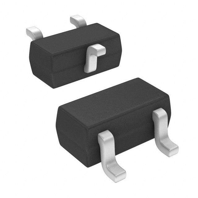
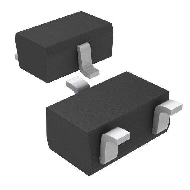
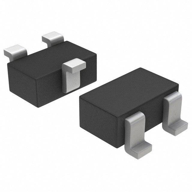
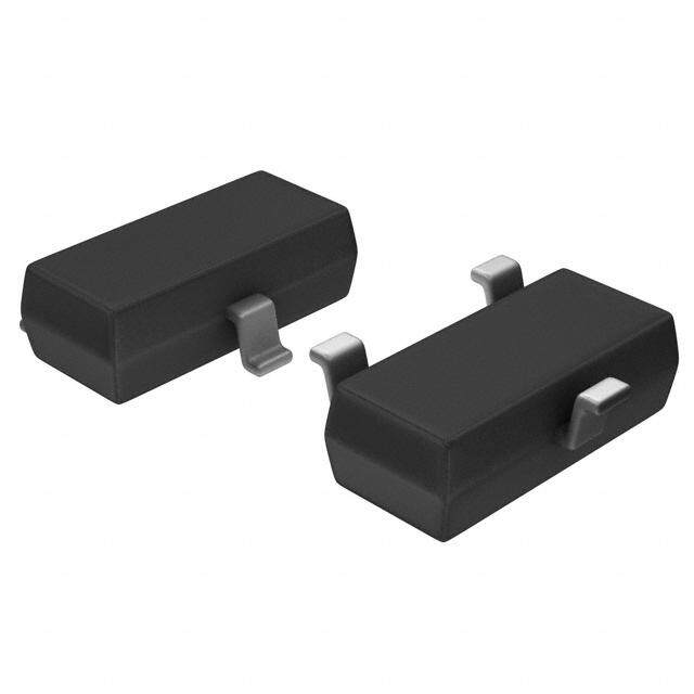
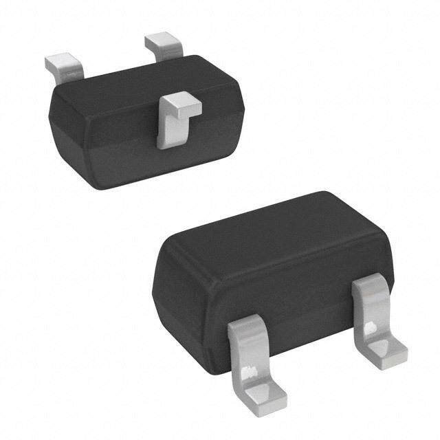
| 供应商器件封装 | ML4-N1 |
| 其它名称 | UNRL11500ACT |
| 功率-最大值 | 150mW |
| 包装 | 剪切带 (CT) |
| 安装类型 | 表面贴装 |
| 封装/外壳 | SC-103 |
| 晶体管类型 | PNP - 预偏压 |
| 标准包装 | 1 |
| 电压-集射极击穿(最大值) | 50V |
| 电流-集电极(Ic)(最大值) | 100mA |
| 电流-集电极截止(最大值) | 500nA |
| 电阻器-发射极基底(R2)(Ω) | - |
| 电阻器-基底(R1)(Ω) | 10k |
| 频率-跃迁 | 80MHz |


- 商务部:美国ITC正式对集成电路等产品启动337调查
- 曝三星4nm工艺存在良率问题 高通将骁龙8 Gen1或转产台积电
- 太阳诱电将投资9.5亿元在常州建新厂生产MLCC 预计2023年完工
- 英特尔发布欧洲新工厂建设计划 深化IDM 2.0 战略
- 台积电先进制程称霸业界 有大客户加持明年业绩稳了
- 达到5530亿美元!SIA预计今年全球半导体销售额将创下新高
- 英特尔拟将自动驾驶子公司Mobileye上市 估值或超500亿美元
- 三星加码芯片和SET,合并消费电子和移动部门,撤换高东真等 CEO
- 三星电子宣布重大人事变动 还合并消费电子和移动部门
- 海关总署:前11个月进口集成电路产品价值2.52万亿元 增长14.8%


PDF Datasheet 数据手册内容提取
Transistors with built-in Resistor UNRL110/111/113/114/115 Silicon PNP epitaxial planer type Unit: mm For digital circuit / 0.020±0.010 e 3 2 (cid:1)•MFoelad tluearedlsess type package, allowing downsizing and thinncing of ±0.800.05 4 1 •tThhee e PqCuiBp mmeonutn atinndg a aurteoam isa t1i/c1 i0n osef rtthioant otfh rleoaudg hty tphee ptaancpkea pgaec (k3i-npgi.n 1.00d±0.05 4 0.60±0.05 10.05±0.03 MINI-type package). (cid:1) Resistance by Part Number a ue 0.20±0.03 stage. 0.50 •UNRL110 MarkingP Symbol 4(7R k1Ω)n(R2) 0.30y±0c.0l33e 0.60 20.05±0.03 n c ••UUNNRRLL111113 AB e4170 kkΩΩ 1407 kkΩΩ ct life 12:: EBmasietter •UNRL114 R 10 kΩ 47 kΩi du 3: Collector •UNRL115 Mt10 kΩ t ro 4: Collector n n r P ML4-N1 Package u (cid:1) Absolute Maximum Ratings T = 25°C o i oa g f pe n. Parameter Symbol Rating Unit n y o (cid:1)NCCCTJSouttooooEMeontlll)racllllaeeeelt* gicccpo:cttetoooonPa ttwrrr rrret eiiettcmeacnaoomur:ta p erebdp2redlmaiee0 rs sCnarc.sie0Datttiit urtp hveumcraroaueirt meliivrtotoa a2nbg lo ctoe*aratg ermesdro icrsoectp,i epct/hescircD VVifk ToTPsTInCCsiCTBeEtljacg OsO f=oso:r n 12 tci.5o6n°l −mlCue5cm5e −t ±−−11otd1o52r55 0i 3 0500p+0p°nol1Crc2alt5ionunedde plsm mmam°°fVVCCWaAnaoiillenntotd eewdindiniasasncncwcocioenenn tI ttintgi yntnepuUurenemeRiaddLc l t toCayynob.pp34nopeenuadet nclataitsoneosntiR ic1.ncRfo2o.rj12pm/aetin/ Collector cuPtoafrfa cmurertenentrtenan SyICmBbOol VCB = −50 V,C IEsoi n=t d f0itoilolnosww.se Min Typ −M 0a.x1 UµnAit Ecumrriettnetr cutoff MUUaiNNRRLL111141 IICEBEOO VVCEBE ==e −−a56s0 V eV , ,Iv iCI Bh=t =t 0 p0://w −−− 000...552 mA Pl UNRL113 − 0.1 UNRL110/115 − 0.01 Collector to base voltage V I = −10 µA, I = 0 −50 V CBO C E Collector to emitter voltage V I = −2 mA, I = 0 −50 V CEO C B Forward current UNRL111 h V = −10 V, I = −5 mA 35 FE CE C transfer ratio UNRL113/114 80 UNRL110/115 160 460 Collector to emitter saturation voltage V I = −10 mA, I = − 0.3 mA − 0.25 V CE(sat) C B Publication date: July 2001 SJH00044AED 1
UNRL110/111/113/114/115 (cid:1) Electrical Characteristics(continued) T = 25°C ± 3°C a Parameter Symbol Conditions Min Typ Max Unit High-level output voltage V V = −5 V, V = − 0.5 V, R = 1 kΩ −4.9 V OH CC B L Low-level output voltage V V = −5 V, V = −2.5 V, R = 1 kΩ − 0.2 V OL CC B L UNRL113 V = −5 V, V = −3.5 V, R = 1 kΩ CC B /L Transition frequency f V = −10 V, I = 1 mA, f = 200 MHz 80 MHz T CB E e Input resistance UNRL111/114/115 R −30% 10 +30% kΩ 1 UNRL110/113 c 47 Resistance ratio UNRL111/113 R/R d0.8 1.0 1.2 1 2 UNRL114 n 0.17 0.21 0.25 e e. a g a u st e n cl y n c Common characteristics chart e PT Ta e i uct lif 180 t t od r )W 160 n n ur P m 140 o (Total power dissipation P TCMh11420862a00000000racAt2me0abriisei4nt0ti cDtesm6 0icpehraa8t0urrtes 1s 0To0af (U1°2CN0)cRD1i4Ls01c1o0ontinued ipnlcalnuedde pls mamfanaoiillenntotd eewdindininasasgncnc fcocoenen t ttitgi ynynpuUpueeeeRddL ttoayynb.ppopeeuadt nlaatseosnti ic.ncfoo.rjpm/aetin/on. I V ce/ V I win mic h I C CE n CE(sat) C o e FE C ()Collector current I mAC−−−−−−11208642000000 IB = −−1 0.0.−9 m 0m.A8A m−MA 0a.7i −mn t0A.6e− m 0nA.5−a Tm0a.−−− A4= 000 m2...1235A °mmmCAAA ()ollector to emitter saturation voltage V VCE(sat)−−−−0−−1.00−−0130..31313000 −P2l5°eCas25e °CvihsitTtta fp=: I7o/Cl5/ l°/ CIwB =w 10w.s Forward current transfer ratio hFE123400000000 TaV 2−=52C °E75C 5°=C° C–10 V C 0 −0.01 0 0 −2 −4 −6 −8 −10 −12 −0.1 −0.3 −1 −3 −10 −30 −100 −1 −3 −10 −30 −100 −300 −1 000 Collector to emitter voltage VCE (V) Collector current IC (mA) Collector current IC (mA) 2 SJH00044AED
UNRL110/111/113/114/115 C V I V V I ob CB O IN IN O 6 fI E= = 1 0 MHz −10 000 VTaO = = 2 −55° CV −100 TVaO = = 2 −5 °0C.2 V )pF 5 Ta = 25°C −3 000 −30 (ector output capacitance C ob 432 µ()Output current I AO−−−1−−13 01300000000 nce/()Input voltage V VINd−−−00−−1..13130 Coll 1 −3 e−0.03 e. −00.C1ol−le0c.3tor t−o1 base− 3volta−g1e0 V−C3B0 (V−)100 −−10a.4 −0In.6put −v0o.l8tage− 1V.0IN (V−u1).2 −1.4 −0.0−10.1 −0O.3utpu−t1 ec ursr−te3nat g IO−1 0(mA−3)0 −100 n cl y n c e Characteristics charts of UNeRL111 ct lif I V iV I u h I C CE CE(sat) C d FE C ()Collector current I mAC−−−−−−−−1111M428640620000000000Coll−ea2ctori to−I 4eBDm =i −tit1−e.r60 nv molAta−−tg8 0se.T 9 Va m −−−−−−−−=−C 00000000A 1E2........ 0617328545 ( °mmmmmmVmmCcAA)AAAAAA−Di12scoon()tCollector to emitter saturation voltage V ViCE(sat)−−n−−−00−−100u..−−13000..−131300013e0.nd1 i−pnC−l0t2.oc3a5ll°lneCuce−td2o15dre° pcClsu m−ramfr3aenaoinillten n t−otId1C e0e w TIdi(nCdinam i /=n−a saAIs 3B7gnc0 )5nc= °fc ocC1o0−oenen 1t tuti0tgi0r yn ynpuUpuPreeeeRForward current transfer ratio hoddLFE tto11ayy4826n00000b.pp−1opeVeCuadEt n=−Cl 3−aoa1lts0le Veoc−t1son0tir cic.u−nr3cfr0eono.rtj − I1pCm0/ 0 a(eTtm−ian A−3=2/o025 )705°n5°C.°C−C1 000 C V ce/ I V win mic V I ob CB n O IN o e IN O ()ctor output capacitance C pFob 65432 MaintenafIT E=a = =1 0 2M5°HCz µ()Output current I AO–−−1−−130−−13 00013000000000000 Please vihsittt fp:o/VTl/laO = =w 2−5w5° CVw.s ()Input voltage V VIN−−−−−100−−130..1313000 VTaO = = 2 −5 0°C.2 V e Coll 1 −3 −0.03 0 −1 −0.01 −0.1 −0.3 −1 −3 −10 −30 −100 −0.4 −0.6 −0.8 −1.0 −1.2 −1.4 −0.1 −0.3 −1 −3 −10 −30 −100 Collector to base voltage VCB (V) Input voltage VIN (V) Output current IO (mA) SJH00044AED 3
UNRL110/111/113/114/115 Characteristics charts of UNRL113 I V V I h I C CE CE(sat) C FE C −160 IB = −1.0 mA Ta = 25°C )V−100 IC / IB = 10 400 VCE = −10 V ()Collector current I mAC−−−−−−−11142840620000000 − 0−.−9 0− 0m. −8.0−−−−7A . 00m000 6m..... 3421A5mA mmmmmAAAAAA (ollector to emitter saturation voltage V CE(sat)−−−0−−00.−−130..1313003a−25°Cn25°C cTa =e 75°C/eForward current transfer ratio hFEd123000000 age.Ta −=22 575°5°C°CC 00 −2 −4 −6 −8 −10 −12 C−0.0−10.1 −0.3 −1 −3 −10 u−30 −100 0−1 −3 −10e s−t30 −100 −300 −1 000 Collector to emitter voltage VCE (V) n Collector current IC (mA) Colyleccltor current IC (mA) n c e C V e I V ct lif V I ob CB iO IN u IN O ()Collector output capacitance C pFob M−06543210.C1ol−le0ac.3tori t−o1 Dbasie− 3vnolta−gt1es0 fIT EV=a = =−C1 30B 2M0 5 °(HCVcz−D)1i0s0coonµ()tOutput current I AiO−−−n1−−130−−13 000u−−1300000−130000000e0.nd4 ipnlt−c0Ialn.6pnuuedt −vde0o p.lsl8t maamfgaenaoiil− le1Vnn.t0otdIN ee w di(nVTdinV−iaOn1a s)a= s.=2 gnc2 nc −5fc5oc°o CVoe−nen t1 tuti.tgi4r yn ynpuUpuPreeeeR()Input voltage V VoddLIN d−−t−to−−00−−1ay..00y−−00130n..−131313000b.pp0op.e1euadt− n0lO.a3autstpeou−st1n tic uicr.r−necf3noto .r jIO−p1 m /0VT(maaeO t= Ai=−n 2 3/)−o500°n.C2. −V100 Characteristics charts of cUe/NRL114 win mic n o e ()Collector current I mAC−−−−−−−111142864060000000 IB = −1IM.C0 amiAnt VeCn−E 0aT−.9 a0 −−−−−−m=.8 000000 A2 ......m5367245 °AmmmmmmCAAAAAA ()o emitter saturation voltage V VCE(sat)−−−−−100−−130..1313000 PleVa2sC5°EeC( savti) hsittt fpIT:CIo/aCl /= l/ 7IwB5 °=Cw 10w.s ward current transfer ratio hFE123400000000 hFE ICTaV2− =52C °E57C °5=C° −C10 V −20 − 0.1 mA Collector t−0.03 −25°C For 00 −2 −4 −6 −8 −10 −12 −0.0−10.1 −0.3 −1 −3 −10 −30 −100 0−1 −3 −10 −30 −100 −300 −1 000 Collector to emitter voltage VCE (V) Collector current IC (mA) Collector current IC (mA) 4 SJH00044AED
UNRL110/111/113/114/115 C V I V V I ob CB O IN IN O )F 6 fIT E=a = =1 0 2M5°HCz –−130 000000 VTaO = = 2 −55° CV −1− 300000 VTaO = = 2 −50°.C2 V p 5 (ector output capacitance C ob 432 µ()Output current I AO−−−1–−13 01300000000 nce/()Input voltage V VIN−d−−1−−13013000 Coll 1 −3 e−0.3 e. 0 −1a −0.1 g −0.1 −0.3 −1 −3 −10 −30 −100 −0.4 −0.6 −0.8 −1.0 −1.2 −1.4 −0.1 −0.3 −1 −3a −10 −30 −100 Collector to base voltage VCB (V) Input voltage VIN (Vu) Output ec ursrtent IO (mA) n cl y n c e CharacteristicIs ch aVrts of UNeRL115 iV I uct lif h I C CE CE(sat) C d FE C −160 t −100 t ro 400 ()Collector current I mAC−−−M−−−−1114284062000000000Coll−eaI2cBt o=ri − t1o−. D40e mmiAitt−er6n volta−−g8se 0T . −9Va −−−−−−−0=m−C . 0000000 81EA2....... 073216545 m( °mmmmVmmmcACD)AAAAAAA−i1s2coon()tCollector to emitter saturation voltage V ViCE(sat)−−n−−00−−00..u−−1300..−13130013e0.nd1 i−pnC−l02.oc3a5ll°lnCeuc−etdo1dre pclsu2 m−5ramfr°3aeCnaoinillten n t−otId1C e0e TwI d(iCnadinm i/=n −asI aAs73Bgn 5c0)n=c ° fcCo1co0−oenen 1t tut0itgi0r yn ynpuUpuPeeeeRForward current transfer ratio hddLFE tto123ayy000nb.0000pp−1opeeuadt n−Cl3aoaltsleeoc−t1son0tir cic.u−nr3cfr0eoon.rtjT − aI1p Cm=0/V −0 27a(Ce255tmE5i−°° n°=CCA3/Co 0−)01n0.− V1 000 C V ce/ I V win mic V I ob CB n O IN o e IN O ()ctor output capacitance C pFob 65432 MaintenafIT E=a = =1 0 2M5°HCz µ()Output current I AO−−−1−−130−−13 00013000000000000 Please vihsittt fp:o/lVT/laO = w= 2 −5w5˚C Vw.s ()Input voltage V VIN−−−−−100−−130..1313000 VTaO = = 2 −50°.C2 V e Coll 1 −3 −0.03 0 −1 −0.01 −0.1 −0.3 −1 −3 −10 −30 −100 −0.4 −0.6 −0.8 −1.0 −1.2 −1.4 −0.1 −0.3 −1 −3 −10 −30 −100 Collector to base voltage VCB (V) Input voltage VIN (V) Output current IO (mA) SJH00044AED 5
Request for your special attention and precautions in using the technical information and semiconductors described in this book (1)(cid:9)If any of the products or technical information described in this book is to be exported or provided to non-residents, the laws and regulations of the exporting country, especially, those with regard to security export control, must be observed. (2)(cid:9)The technical information described in this book is intended only to show the main characteristics and application circuit examples of the products, and no license is granted under any intellectual property right or other right owned by our company or any other company. Therefore, no responsibility is assumed by our company as to the infringement upon any such right owned by any other company which may arise as a result of the use of technical information described in this book. (3)(cid:9)The products described in this book are intended to be used for standard applications or general electronic equipment (such as office / equipment, communications equipment, measuring instruments and household appliances). Consult our sales staff in advance for information on the following applicateions: (cid:150) Special applications (such as for airplanes, aerospace, automobiles, traffic control equipment, combustion equipment, life support systems and safety devices) in which exceptional quality and reliability are required, or if the failure or malfunction of the prod- c ucts may directly jeopardize life or harm the human body. (cid:150) Any applications other than the standard applications intended. d n (4)(cid:9)The products and product specifications described in this book are subject to change without notice for modification and/or im- e provement. At the final stage of your design, purchasing, or use of the products, therefore, ask for the most upe-t.o-date Product Standards in advance to make sure that the latest spaecifications satisfy your requirements. ag u st (5)(cid:9)When designing your equipment, comply with the range of absolute maximum rating and the guarantee ed operating conditions (operating power supply voltage and opernating environment etc.). Especially, please be careful not to yexclceed the range of absolute maximum rating on the transient state, such as power-on, power-onff and mode-switching. Otherwiseec, we will not be liable for any (cid:9) dEevfeecnt wwhheicnh t hmea pyr aordiusec tlsa taerre i nu syeodeu wr eitqhuinip tmhee ngt.uaranteed values, take into the consideration ocf ti nlicfidence of break down and failure i u mode, possible to occur to semiconductor products. Measures on the systems such as redudndant design, arresting the spread of fire or preventing glitch are retcommended in order to prevetnt physical injury, fire, social damoages, for example, by using the products. r n n r P (6)(cid:9)Comply with the instructions for use in order to prevent breakdown and characteruistics change due to external factors (ESD, EOS, o tdhaemrmp-apl rostorfe spisa caknidn gm iesc rheaqnuiicraeld s, tsraetsiss)f ya tt hteho ec otinmdiet ioofn sh, asnudclhin ags, smheoluf nlitfine ga nodnr gtah tfe c eulsatpoysmepdeer t'sim per oscinecsse. fWirsht eonp eunsiinngg tphreo dpuaccktsa ogfoenrs. .which (7)(cid:9)TEMhleics trbioc oIkna dmusatyriD abl eCi noo.,t Lrtedps.rinted coDri srecproondtuicnedu ewdh ietpnhlecalr nuwedhdoe pllsly mamf aonaoiilrl ennptotda erewtdinidinaialsaslyncnc,c ocowenen ti tttitgih ynonupuUute eeRthddL e t topayynrb.pipoopere uadwt nrliatattseneo spntie ricm.ncfisoso.irjonpm/ oaetfi nM/atsushita ce/ win mic n o e ntena sit follww.s ai vi w M se p:// ea htt Pl