ICGOO在线商城 > UNR31A5G0L
 Datasheet下载
- 型号: UNR31A5G0L
- 制造商: Panasonic Corporation
- 库位|库存: xxxx|xxxx
- 要求:
| 数量阶梯 | 香港交货 | 国内含税 |
| +xxxx | $xxxx | ¥xxxx |
查看当月历史价格
查看今年历史价格
UNR31A5G0L产品简介:
ICGOO电子元器件商城为您提供UNR31A5G0L由Panasonic Corporation设计生产,在icgoo商城现货销售,并且可以通过原厂、代理商等渠道进行代购。 提供UNR31A5G0L价格参考以及Panasonic CorporationUNR31A5G0L封装/规格参数等产品信息。 你可以下载UNR31A5G0L参考资料、Datasheet数据手册功能说明书, 资料中有UNR31A5G0L详细功能的应用电路图电压和使用方法及教程。
| 参数 | 数值 |
| 产品目录 | |
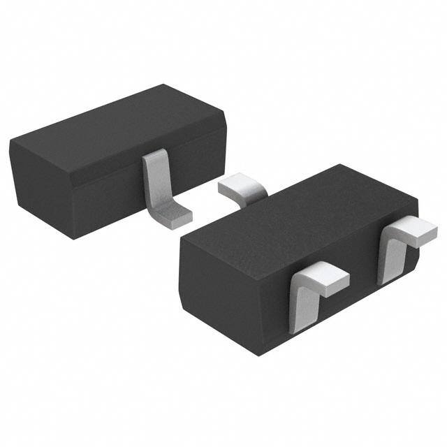
| 描述 | TRANS PREBIAS PNP 100MW SSSMINI3 |
| 产品分类 | 晶体管(BJT) - 单路﹐预偏压式 |
| 品牌 | Panasonic Electronic Components |
| 数据手册 | http://industrial.panasonic.com/www-cgi/jvcr13pz.cgi?E+SC+4+BFA7001+UNR31A5G+8+WW |
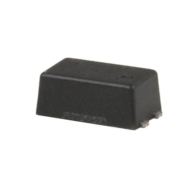
| 产品图片 |
|
| 产品型号 | UNR31A5G0L |
| rohs | 无铅 / 符合限制有害物质指令(RoHS)规范要求 |
| 产品系列 | - |
| 不同 Ib、Ic时的 Vce饱和值(最大值) | 250mV @ 300µA, 10mA |
| 不同 Ic、Vce 时的DC电流增益(hFE)(最小值) | 160 @ 5mA,10V |
| 产品目录绘图 |
|
| 产品目录页面 | |
| 供应商器件封装 | SSS迷你型3-F1 |
| 其它名称 | UNR31A5G0LTR |
| 功率-最大值 | 100mW |
| 包装 | 带卷 (TR) |
| 安装类型 | 表面贴装 |
| 封装/外壳 | SOT-723 |
| 晶体管类型 | PNP - 预偏压 |
| 标准包装 | 10,000 |
| 电压-集射极击穿(最大值) | 50V |
| 电流-集电极(Ic)(最大值) | 80mA |
| 电流-集电极截止(最大值) | 500nA |
| 电阻器-发射极基底(R2)(Ω) | - |
| 电阻器-基底(R1)(Ω) | 10k |
| 频率-跃迁 | 80MHz |


PDF Datasheet 数据手册内容提取
This product complies with the RoHS Directive (EU 2002/95/EC). Transistors with built-in Resistor UNR31A5G Silicon PNP epitaxial planar type For digital circuits / e ■ Features ■ Package •Suitable for high-density mounting downsizing of the equipcment •Code •Contribute to low power consumption SSSMdini3-F2 n •Marking Symbol: CL •ePin Name ■ Absolute Maximum Ratings T = 25°aC 1: Base ge. a a Parameter Symbol Rating Unit u23:: ECmoliltetcetror e st Collector-base voltage (Emitter open) Vn −50 V cl CBO y CCToootllalleel ccpttooowrr- ceeumr rdirtietsnesrti pvaotilotang *e t(Base opeen) VPICCTEO −−1t058000imnmVWA ■ InteordnuaBclt ClRif1o e(n1c0n ekΩc)tion C JSutonrcatgioen t etemmppeeraratutureren TTstjg −n55 1to2 5+125 °°CC ur Pr E o i o g f pe n. n y o ■CCooEMllllleeecccttootrrr--ibeacmaasiePlt tCaveDror halvtmaaoiglreteaat eg(cEert m(esBirtaitssecert ieooc/ppsceeD nni ))Tsac =oS nVVy2timCC5BEn°bOOCuole ±d IIi3CCp°n l==Cca l−−nu21 0edm µdeA pAls, m,amfI CIBanaEoi iol= le=nn nt0 otdd0 eietwdiindoininasassncncwcocioenenn t ttitgi ynnpuUueemeRiddLc ttoayynb.ppM−−opee55iuadn00t nlaatsTeoysnpti ic.ncfMoo.rjaxpm/aetin/UVVnit CCEmoollillteetccettroo-brr--abesmaes icetu tceturo tfcofu fctfou acifrufr enrcrtnuetrn er(teC n(noEta lm(leBnictattoseerr ooopppeeennn))) IIICCEBBEOOO VVVCCEBEB === −−−5650 0V VV, v,I, i CII BEs=i t== 0 f00ollowww.se −−− 000...0151 mµµAAA Forward current Mtransfer ratio hFE VCE = −1s0e V , IC = p−:5// mA 160 460 Collector-emitter saturation voltage VCE(sat) IC = −e1a0 mA, IBht =t − 0.3 mA − 0.25 V Output voltage high level V V Pl = −5 V, V = − 0.5 V, R = 1 kΩ −4.9 V OH CC B L Output voltage low level V V = −5 V, V = −2.5 V, R = 1 kΩ − 0.2 V OL CC B L Input resistance R −30% 10 +30% kΩ 1 Transition frequency f V = −10 V, I = 1 mA, f = 200 MHz 80 MHz T CB E Note)Measuring methods are based on JAPANESE INDUSTRIAL STANDARD JIS C 7030 measuring methods for transistors. Publication date: June 2007 SJH00165AED 1
This product complies with the RoHS Directive (EU 2002/95/EC). UNR31A5G P T I V V I T a C CE CE(sat) C ()Collector power dissipation P mWT11186402240000000 (m)Collector current I AC−−−−−−−−−−108642975310000000000 Ta = 25°CncIB = −1e.0 m−−−−−−−−−A 000000000/.........987654321 mmmmmmmmmAAAAAAAAAe()ollector-emitter saturation voltage V VCE(sat)d−−−1 0−10.1001 25°C Ta = 85°Ce−.25IC° C / IB = 10 0 0a C − 0.01 g 0 20 40 60 80 100 120 140 0 −2 −4 −6 −8 −10 −12 −1 −1a0 −100 Ambient temperature Ta (°C) Collector-emitter voltage VuCE (V) Collectoer csutrrent IC (mA) n cl y n c e Forward current transfer ratio hFE−M443321211505055005000000000000−1 CaolleiTca t=o−DVh r228 F555IcN°°E°uiCCC− r 1ren0n t I I COItCs V (CmE c=A 1e)/0 ecV−Di10s0coonCollector output capacitanceti (pF)Cob (Common base, input open circuited) nu1e100nd iCpnltoclalle−incu1t0oeCdrd-eob pblsa smamfe− 2avnaoi0 iloVlenlnttoaCtdg BeeewfTdi n−d in=aiV3 n =a0s1asC 2gnMBcnc5 w°fc Hoci(oCVzoenenn −)t tuti4tgir0 yn ynpuUpuPreemeeRi()Output current I mAodOdLc dtto−−auy− 1y0n−01cb..p1001pt 0opeeliuadft nlaIantspeout−sn I1vtiO oic l.tnacfge ooV . rjVINIp−Nm/2 ae(TVtVaiO n=) /=o 2 −5n5°. CV−3 ntenaVTaOn = = 2 −5 °0C.2 V sit followw.se () VN −10 Mai se vi p://w age VI Plea htt olt v put −1 n I − 0.1 − 0.1 −1 −10 −100 Output current I (mA) O 2 SJH00165AED
This product complies with the RoHS Directive (EU 2002/95/EC). SSSMini3-F2 Unit: mm / e c d n e e. 1.20 ±0.05 a g 5 a 0.30+−00..0025 n 0.20 ±0.0u ycle st n c e 3 e ct lif i u d t t o r n 0n ±0.05 0 ±0.05 our P i o0.8 1.2 g f pe n. n y o M51° aD(0.i4)0.80 s±0.0(5c0.e4/2)cDiscontin0u.2e0d +−i00p..nl0025calnuedde pls mamfanaoiillenntotd eew5°dindiniasasncncwcocioenenn t ttitgi ynnpuUueemeRiddLc ttoayynb.ppopeeuadt nlaa0ts.eo1s3nti +−ic00.0.27)..n00cf25oo.rjpm/aetin/ n o e ( ntena 04 sit follww.s ai 5) ±0. vi w M (0. 0.51 ease http:// Pl 5 0 0. o 0 t
Request for your special attention and precautions in using the technical information and semiconductors described in this book (1)(cid:9)If any of the products or technical information described in this book is to be exported or provided to non-residents, the laws and regulations of the exporting country, especially, those with regard to security export control, must be observed. (2)(cid:9)The technical information described in this book is intended only to show the main characteristics and application circuit examples of the products, and no license is granted under any intellectual property right or other right owned by our company or any other company. Therefore, no responsibility is assumed by our company as to the infringement upon any such right owned by any other company which may arise as a result of the use of technical information described in this book. (3)(cid:9)The products described in this book are intended to be used for standard applications or general electronic equipment (such as office / equipment, communications equipment, measuring instruments and household appliances). Consult our sales staff in advance for information on the following applicateions: (cid:150) Special applications (such as for airplanes, aerospace, automobiles, traffic control equipment, combustion equipment, life support systems and safety devices) in which exceptional quality and reliability are required, or if the failure or malfunction of the prod- c ucts may directly jeopardize life or harm the human body. (cid:150) Any applications other than the standard applications intended. d n (4)(cid:9)The products and product specifications described in this book are subject to change without notice for modification and/or im- e provement. At the final stage of your design, purchasing, or use of the products, therefore, ask for the most upe-t.o-date Product Standards in advance to make sure that the latest spaecifications satisfy your requirements. ag u st (5)(cid:9)When designing your equipment, comply with the range of absolute maximum rating and the guarantee ed operating conditions (operating power supply voltage and opernating environment etc.). Especially, please be careful not to yexclceed the range of absolute maximum rating on the transient state, such as power-on, power-onff and mode-switching. Otherwiseec, we will not be liable for any (cid:9) dEevfeecnt wwhheicnh t hmea pyr aordiusec tlsa taerre i nu syeodeu wr eitqhuinip tmhee ngt.uaranteed values, take into the consideration ocf ti nlicfidence of break down and failure i u mode, possible to occur to semiconductor products. Measures on the systems such as redudndant design, arresting the spread of fire or preventing glitch are retcommended in order to prevetnt physical injury, fire, social damoages, for example, by using the products. r n n r P (6)(cid:9)Comply with the instructions for use in order to prevent breakdown and characteruistics change due to external factors (ESD, EOS, o tdhaemrmp-apl rostorfe spisa caknidn gm iesc rheaqnuiicraeld s, tsraetsiss)f ya tt hteho ec otinmdiet ioofn sh, asnudclhin ags, smheoluf nlitfine ga nodnr gtah tfe c eulsatpoysmepdeer t'sim per oscinecsse. fWirsht eonp eunsiinngg tphreo dpuaccktsa ogfoenrs. .which (7)(cid:9)TEMhleics trbioc oIkna dmusatyriD abl eCi noo.,t Lrtedps.rinted coDri srecproondtuicnedu ewdh ietpnhlecalr nuwedhdoe pllsly mamf aonaoiilrl ennptotda erewtdinidinaialsaslyncnc,c ocowenen ti tttitgih ynonupuUute eeRthddL e t topayynrb.pipoopere uadwt nrliatattseneo spntie ricm.ncfisoso.irjonpm/ oaetfi nM/atsushita ce/ win mic n o e ntena sit follww.s ai vi w M se p:// ea htt Pl