ICGOO在线商城 > UNR31A0G0L
- 型号: UNR31A0G0L
- 制造商: Panasonic Corporation
- 库位|库存: xxxx|xxxx
- 要求:
| 数量阶梯 | 香港交货 | 国内含税 |
| +xxxx | $xxxx | ¥xxxx |
查看当月历史价格
查看今年历史价格
UNR31A0G0L产品简介:
ICGOO电子元器件商城为您提供UNR31A0G0L由Panasonic Corporation设计生产,在icgoo商城现货销售,并且可以通过原厂、代理商等渠道进行代购。 提供UNR31A0G0L价格参考以及Panasonic CorporationUNR31A0G0L封装/规格参数等产品信息。 你可以下载UNR31A0G0L参考资料、Datasheet数据手册功能说明书, 资料中有UNR31A0G0L详细功能的应用电路图电压和使用方法及教程。
| 参数 | 数值 |
| 产品目录 | |
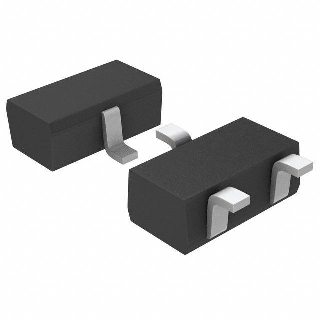
| 描述 | TRANS PREBIAS PNP 100MW SSSMINI3 |
| 产品分类 | 晶体管(BJT) - 单路﹐预偏压式 |
| 品牌 | Panasonic Electronic Components |
| 数据手册 | http://industrial.panasonic.com/www-cgi/jvcr13pz.cgi?E+SC+4+BFA7001+UNR31A0G+8+WW |
| 产品图片 |
|
| 产品型号 | UNR31A0G0L |
| rohs | 无铅 / 符合限制有害物质指令(RoHS)规范要求 |
| 产品系列 | - |
| 不同 Ib、Ic时的 Vce饱和值(最大值) | 250mV @ 300µA, 10mA |
| 不同 Ic、Vce 时的DC电流增益(hFE)(最小值) | 160 @ 5mA,10V |
| 产品目录绘图 |
|
| 产品目录页面 | |
| 供应商器件封装 | SSS迷你型3-F1 |
| 其它名称 | UNR31A0G0LDKR |
| 功率-最大值 | 100mW |
| 包装 | Digi-Reel® |
| 安装类型 | 表面贴装 |
| 封装/外壳 | SOT-723 |
| 晶体管类型 | PNP - 预偏压 |
| 标准包装 | 1 |
| 电压-集射极击穿(最大值) | 50V |
| 电流-集电极(Ic)(最大值) | 80mA |
| 电流-集电极截止(最大值) | 500nA |
| 电阻器-发射极基底(R2)(Ω) | - |
| 电阻器-基底(R1)(Ω) | 47k |
| 频率-跃迁 | 80MHz |




- 商务部:美国ITC正式对集成电路等产品启动337调查
- 曝三星4nm工艺存在良率问题 高通将骁龙8 Gen1或转产台积电
- 太阳诱电将投资9.5亿元在常州建新厂生产MLCC 预计2023年完工
- 英特尔发布欧洲新工厂建设计划 深化IDM 2.0 战略
- 台积电先进制程称霸业界 有大客户加持明年业绩稳了
- 达到5530亿美元!SIA预计今年全球半导体销售额将创下新高
- 英特尔拟将自动驾驶子公司Mobileye上市 估值或超500亿美元
- 三星加码芯片和SET,合并消费电子和移动部门,撤换高东真等 CEO
- 三星电子宣布重大人事变动 还合并消费电子和移动部门
- 海关总署:前11个月进口集成电路产品价值2.52万亿元 增长14.8%

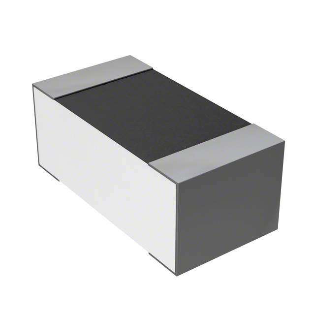

PDF Datasheet 数据手册内容提取
This product complies with the RoHS Directive (EU 2002/95/EC). Transistors with built-in Resistor UNR31A0G Silicon PNP epitaxial planar type / For digital circuits e ■ Features c ■ Package •Suitable for high-density mounting and downsizing of the equipment •Code d . e •Contribute to low power consumption n SSSMini3-F2 g a •Maerking Symbol: CD t s •Pin Name e ■ Absolute Maximum Ratings T = 25°Ca 1: Base cl a u y 2: Emitter c Parameter Symbol Rating Unit e n 3: Collector f Collector-base voltage (Emitter open) VCBO −50 Vn t li Collector-emitter voltage (Base open) VCEO −50 V ■ Internal Councnection Collector current e IC −80 imA roRd (47 kΩ) Total power dissipation P 100 mW P 1 C T t B Junction temperature t Tj n125 °C ur . Storage temperaturen Tstg −55 to +125 °C g fo pe E tion n y a i o wi e t d m r a c s folloenance typed type st info ■MElectricaDl Ciharacsteristics Ta = 25e°Cd i ±n 3c°lnCuedd e maiaintntensacnocntinnuueed taybpoeut nleatt/esc/en CCoolllleeccttoorr--bemasiePt taveror alvtmaogleteat eg(Eer m(Bitatseesr oocppoeennn))tinSVVyumCCBEbOOolplIIaCC == −−21pl 0m aµmAAn, ,I CeIBE o= d=n 0 d0ddiiitiosncsonngt iU nRaL soM−−n55iin00c. Typ Max UVVnit Collector-base cutoff current (EmDiitter open) ICBO VCB = −50 V, IE = 0 wi a − 0.1 µA CEFmoorlilwtetceatror-dbr-a ecsmue rictruteetnro nftcf ut cartouafrnnfr seccfnuetr rer( eC/rnaottl i(loeBcatoser ooppeenn)) IIhCEFBEEOO VVVCECBEE === −−−56100 Vs iVV,t ,,I CfII CB= o== l0l −0o5h tmtAp://p 160 −−4 060.0.051 mµAA Collector-netmeitter saturation voltage VCE(sat) IC = e− 1v0i mA, IB = − 0.3 mA − 0.25 V OutpMuta ivoltage high-level VOH aVCsC = −5 V, VB = − 0.5 V, RL = 1 kΩ −4.9 V Output voltage low-level V eV = −5 V, V = −2.5 V, R = 1 kΩ − 0.2 V OLPl CC B L Input resistance R −30% 47 +30% kΩ 1 Transition frequency f V = −10 V, I = 1 mA, f = 200 MHz 80 MHz T CB E Note)Measuring methods are based on JAPANESE INDUSTRIAL STANDARD JIS C 7030 measuring methods for transistors. Publication date: June 2007 SJH00160AED 1
This product complies with the RoHS Directive (EU 2002/95/EC). UNR31A0G P T I V V I T a C CE CE(sat) C ()Total power dissipation P mWT11208642000000 Collector current I (mA)C−−−−86420000 T−a 0=.− 62 05m.°7AC mA− 0.8− m0.A9 mAIB =−− −−−− 001000......540132 mmmmmmAAAAAA ctor-emitter saturation voltage V (V)CE(sat)−− 0−1.011 25T°Ca = 85°C −25°C e 00 40 80 120 00 −2 −4 −6 −8 −10 −12 Coll− 0.0−1 0.1 −1 −10IC / IB = 10−100 Ambient temperature Ta (°C) Collector-emitter voltage VCE (V) Collector current IC (mA) h I C V I V FE C ob CB O IN E400 Ta = 85°C VCE = −10 V (pF)Cob 10 fT =a =1 2M5°HCz −10 VTaO = = 2 −55° CV Forward current transfer ratio hF312000000 −2255°°CC or output capacitancemon base, input open circuited) Output current I (mA)O −1 ctm 0 Colle (Co 1 − 0.1 −1 −10 −100 0 −8 −16 −24 −32 −40 0 − 0.8 −1.6 Collector current IC (mA) Collector-base voltage VCB (V) Input voltage VIN (V) V I IN O −10 VO = − 0.2 V Ta = 25°C V) (N VI ge −1 a olt v ut p n I − 0.1 − 0.1 −1 −10 −100 Output current I (mA) O 2 SJH00160AED
This product complies with the RoHS Directive (EU 2002/95/EC). SSSMini3-F2 Unit: mm 1.20 ±0.05 5 0 0. 0.30+−00..0025 20 ± 0. 3 0 ±0.05 0 ±0.05 8 2 0. 1. ° 5 1 2 0.20+−00..0025 0.13+−00..0025 (0.4) (0.4) 0.80 ±0.05 5° 7) 2 0. ( 4 0 5) ±0. 0. 1 ( 5 0. 5 0 0. o 0 t
Request for your special attention and precautions in using the technical information and semiconductors described in this book (1)(cid:9)If any of the products or technical information described in this book is to be exported or provided to non-residents, the laws and regulations of the exporting country, especially, those with regard to security export control, must be observed. (2)(cid:9)The technical information described in this book is intended only to show the main characteristics and application circuit examples of the products, and no license is granted under any intellectual property right or other right owned by our company or any other company. Therefore, no responsibility is assumed by our company as to the infringement upon any such right owned by any other company which may arise as a result of the use of technical information described in this book. (3)(cid:9)The products described in this book are intended to be used for standard applications or general electronic equipment (such as office equipment, communications equipment, measuring instruments and household appliances). Consult our sales staff in advance for information on the following applications: (cid:150) Special applications (such as for airplanes, aerospace, automobiles, traffic control equipment, combustion equipment, life support systems and safety devices) in which exceptional quality and reliability are required, or if the failure or malfunction of the prod- ucts may directly jeopardize life or harm the human body. (cid:150) Any applications other than the standard applications intended. (4)(cid:9)The products and product specifications described in this book are subject to change without notice for modification and/or im- provement. At the final stage of your design, purchasing, or use of the products, therefore, ask for the most up-to-date Product Standards in advance to make sure that the latest specifications satisfy your requirements. (5)(cid:9)When designing your equipment, comply with the range of absolute maximum rating and the guaranteed operating conditions (operating power supply voltage and operating environment etc.). Especially, please be careful not to exceed the range of absolute maximum rating on the transient state, such as power-on, power-off and mode-switching. Otherwise, we will not be liable for any defect which may arise later in your equipment. (cid:9) Even when the products are used within the guaranteed values, take into the consideration of incidence of break down and failure mode, possible to occur to semiconductor products. Measures on the systems such as redundant design, arresting the spread of fire or preventing glitch are recommended in order to prevent physical injury, fire, social damages, for example, by using the products. (6)(cid:9)Comply with the instructions for use in order to prevent breakdown and characteristics change due to external factors (ESD, EOS, thermal stress and mechanical stress) at the time of handling, mounting or at customer's process. When using products for which damp-proof packing is required, satisfy the conditions, such as shelf life and the elapsed time since first opening the packages. (7)(cid:9)This book may be not reprinted or reproduced whether wholly or partially, without the prior written permission of Matsushita Electric Industrial Co., Ltd.
 Datasheet下载

