ICGOO在线商城 > 集成电路(IC) > PMIC - 配电开关,负载驱动器 > ULQ2004AD
 Datasheet下载
- 型号: ULQ2004AD
- 制造商: Texas Instruments
- 库位|库存: xxxx|xxxx
- 要求:
| 数量阶梯 | 香港交货 | 国内含税 |
| +xxxx | $xxxx | ¥xxxx |
查看当月历史价格
查看今年历史价格
ULQ2004AD产品简介:
ICGOO电子元器件商城为您提供ULQ2004AD由Texas Instruments设计生产,在icgoo商城现货销售,并且可以通过原厂、代理商等渠道进行代购。 ULQ2004AD价格参考¥1.41-¥4.05。Texas InstrumentsULQ2004AD封装/规格:PMIC - 配电开关,负载驱动器, 。您可以下载ULQ2004AD参考资料、Datasheet数据手册功能说明书,资料中有ULQ2004AD 详细功能的应用电路图电压和使用方法及教程。
Texas Instruments(德州仪器)的ULQ2004AD是一款属于PMIC(电源管理集成电路)分类下的配电开关和负载驱动器产品。该型号的应用场景主要包括以下几个方面:

1. LED驱动:
   ULQ2004AD可以用于驱动小型LED指示灯或背光应用,适用于消费电子设备、家用电器和工业控制面板中的状态指示。

2. 继电器和小型电机控制:
   该器件能够为低功率继电器或小型直流电机提供驱动电流,适合应用于自动化设备、家用电器和汽车电子中的简单机电控制。

3. 多负载切换:
   在需要对多个负载进行独立开关控制的系统中,例如打印机、扫描仪或多通道电源管理系统中,ULQ2004AD可以实现高效的负载分配与切换。

4. 通信接口电路:
   在RS-232、RS-485等通信接口中,该器件可用于信号电平转换或增强驱动能力,以确保可靠的数据传输。

5. 电池供电设备:
   针对便携式设备(如手持终端、遥控器或医疗设备),ULQ2004AD以其低功耗特性支持电池供电环境下的负载驱动需求。

6. 传感器激励:
   在工业自动化或物联网(IoT)领域,该芯片可用于驱动压力、温度或其他类型的传感器,为其提供稳定的激励信号。

总结来说,ULQ2004AD凭借其高可靠性、低功耗和多通道输出的特点,广泛适用于消费电子、工业控制、汽车电子以及通信设备等领域,满足各种中小功率负载的驱动与控制需求。
| 参数 | 数值 |
| 产品目录 | |
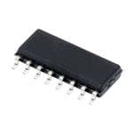
| 描述 | TRANS 7 NPN DARL 50V 500MA 16SO达林顿晶体管 Hi-Vltg Hi-Crnt Darl Transistor Array |
| 产品分类 | 晶体管(BJT) - 阵列分离式半导体 |
| 品牌 | Texas Instruments |
| 产品手册 | |
| 产品图片 |
|
| rohs | 符合RoHS无铅 / 符合限制有害物质指令(RoHS)规范要求 |
| 产品系列 | 晶体管,达林顿晶体管,Texas Instruments ULQ2004AD- |
| 数据手册 | |
| 产品型号 | ULQ2004AD |
| 不同 Ib、Ic时的 Vce饱和值(最大值) | 1.6V @ 500µA, 350mA |
| 不同 Ic、Vce 时的DC电流增益(hFE)(最小值) | - |
| 产品种类 | |
| 供应商器件封装 | 16-SOIC |
| 其它名称 | 296-34766-5 |
| 功率-最大值 | - |
| 包装 | 管件 |
| 单位重量 | 141.300 mg |
| 商标 | Texas Instruments |
| 安装类型 | 表面贴装 |
| 安装风格 | SMD/SMT |
| 封装 | Tray |
| 封装/外壳 | 16-SOIC(0.154",3.90mm 宽) |
| 封装/箱体 | SOIC-16 |
| 工厂包装数量 | 40 |
| 晶体管极性 | NPN |
| 晶体管类型 | 7 NPN 达林顿 |
| 最大工作温度 | + 85 C |
| 最大直流电集电极电流 | 0.5 A |
| 最小工作温度 | - 40 C |
| 标准包装 | 40 |
| 电压-集射极击穿(最大值) | 50V |
| 电流-集电极(Ic)(最大值) | 500mA |
| 电流-集电极截止(最大值) | - |
| 系列 | ULQ2004A |
| 配置 | Array 7 |
| 集电极—发射极最大电压VCEO | 50 V |
| 频率-跃迁 | - |


- 商务部:美国ITC正式对集成电路等产品启动337调查
- 曝三星4nm工艺存在良率问题 高通将骁龙8 Gen1或转产台积电
- 太阳诱电将投资9.5亿元在常州建新厂生产MLCC 预计2023年完工
- 英特尔发布欧洲新工厂建设计划 深化IDM 2.0 战略
- 台积电先进制程称霸业界 有大客户加持明年业绩稳了
- 达到5530亿美元!SIA预计今年全球半导体销售额将创下新高
- 英特尔拟将自动驾驶子公司Mobileye上市 估值或超500亿美元
- 三星加码芯片和SET,合并消费电子和移动部门,撤换高东真等 CEO
- 三星电子宣布重大人事变动 还合并消费电子和移动部门
- 海关总署:前11个月进口集成电路产品价值2.52万亿元 增长14.8%


PDF Datasheet 数据手册内容提取
Product Order Technical Tools & Support & Folder Now Documents Software Community ULN2002A,ULN2003A,ULN2003AI ULQ2003A,ULN2004A,ULQ2004A SLRS027P–DECEMBER1976–REVISEDAUGUST2019 ULN200x, ULQ200x High-Voltage, High-Current Darlington Transistor Arrays 1 Features The ULx2004A devices have a 10.5-kΩ series base resistor to allow operation directly from CMOS • 500-mA-RatedCollectorCurrent(SingleOutput) 1 devices that use supply voltages of 6 V to 15 V. The • High-VoltageOutputs:50V required input current of the ULx2004A device is • OutputClampDiodes belowthatoftheULx2003Adevices, and the required voltage is less than that required by the ULN2002A • InputsCompatibleWithVariousTypesofLogic device. • Relay-DriverApplications . 2 Applications DeviceInformation(1) • RelayDrivers PARTNUMBER PACKAGE BODYSIZE(NOM) • StepperandDCBrushedMotorDrivers ULx200xD SOIC(16) 9.90mm×3.91mm • LampDrivers ULx200xN PDIP(16) 19.30mm×6.35mm • DisplayDrivers(LEDandGasDischarge) ULN200xNS SOP(16) 10.30mm×5.30mm • LineDrivers ULN200xPW TSSOP(16) 5.00mm×4.40mm • LogicBuffers (1) For all available packages, see the orderable addendum at theendofthedatasheet. 3 Description . The ULx200xA devices are high-voltage, high-current . Darlington transistor arrays. Each consists of seven NPN Darlington pairs that feature high-voltage SimplifiedBlockDiagram outputs with common-cathode clamp diodes for switchinginductiveloads. 9 COM The collector-current rating of a single Darlington pair 1 16 1B 1C is 500 mA. The Darlington pairs can be paralleled for higher current capability. Applications include relay 2 15 drivers, hammer drivers, lamp drivers, display drivers 2B 2C (LED and gas discharge), line drivers, and logic buffers. For 100-V (otherwise interchangeable) 3 14 versions of the ULx2003A devices, see the SLRS023 3B 3C datasheetfortheSN75468andSN75469devices. 4 13 TheULN2002Adeviceisdesignedspecificallyforuse 4B 4C with 14-V to 25-V PMOS devices. Each input of this device has a Zener diode and resistor in series to 5 12 5B 5C control the input current to a safe limit. The ULx2003Adeviceshavea2.7-kΩ seriesbase resistor 6 11 for each Darlington pair for operation directly with 6B 6C TTLor5-VCMOSdevices. 7 10 7B 7C 1 An IMPORTANT NOTICE at the end of this data sheet addresses availability, warranty, changes, use in safety-critical applications, intellectualpropertymattersandotherimportantdisclaimers.PRODUCTIONDATA.
ULN2002A,ULN2003A,ULN2003AI ULQ2003A,ULN2004A,ULQ2004A SLRS027P–DECEMBER1976–REVISEDAUGUST2019 www.ti.com Table of Contents 1 Features.................................................................. 1 7 ParameterMeasurementInformation................10 2 Applications........................................................... 1 8 DetailedDescription............................................ 12 3 Description............................................................. 1 8.1 Overview.................................................................12 4 RevisionHistory..................................................... 2 8.2 FunctionalBlockDiagrams.....................................12 5 PinConfigurationandFunctions......................... 3 8.3 FeatureDescription.................................................13 8.4 DeviceFunctionalModes........................................13 6 Specifications......................................................... 4 9 ApplicationandImplementation........................ 14 6.1 AbsoluteMaximumRatings......................................4 6.2 ESDRatings..............................................................4 9.1 ApplicationInformation............................................14 6.3 RecommendedOperatingConditions.......................4 9.2 TypicalApplication .................................................14 6.4 ThermalInformation..................................................4 9.3 SystemExamples...................................................17 6.5 ElectricalCharacteristics:ULN2002A.......................5 10 PowerSupplyRecommendations..................... 18 6.6 ElectricalCharacteristics:ULN2003Aand 11 Layout................................................................... 18 ULN2004A..................................................................5 11.1 LayoutGuidelines.................................................18 6.7 ElectricalCharacteristics:ULN2003AI......................6 11.2 LayoutExample....................................................18 6.8 ElectricalCharacteristics:ULN2003AI .....................6 12 DeviceandDocumentationSupport................. 19 6.9 ElectricalCharacteristics:ULQ2003Aand 12.1 DocumentationSupport........................................19 ULQ2004A.................................................................7 12.2 RelatedLinks........................................................19 6.10 SwitchingCharacteristics:ULN2002A,ULN2003A, 12.3 CommunityResources..........................................19 ULN2004A..................................................................7 12.4 Trademarks...........................................................19 6.11 SwitchingCharacteristics:ULN2003AI ..................7 12.5 ElectrostaticDischargeCaution............................19 6.12 SwitchingCharacteristics:ULN2003AI ..................8 12.6 Glossary................................................................19 6.13 SwitchingCharacteristics:ULQ2003A,ULQ2004A 8 13 Mechanical,Packaging,andOrderable 6.14 TypicalCharacteristics............................................8 Information........................................................... 19 4 Revision History NOTE:Pagenumbersforpreviousrevisionsmaydifferfrompagenumbersinthecurrentversion. ChangesfromRevisionO(January2016)toRevisionP Page • ChangedULN200xAMinimumTemperatureRatingfrom–20Cto–40CintheAbsoluteMaximumRatingstable............4 ChangesfromRevisionN(June2015)toRevisionO Page • ChangedPinFunctionstabletocorrecttypographicalerror ................................................................................................. 3 ChangesfromRevisionM(February2013)toRevisionN Page • AddedPinConfigurationandFunctionssection,ESDRatingstable,FeatureDescriptionsection,DeviceFunctional Modes,ApplicationandImplementationsection,PowerSupplyRecommendationssection,Layoutsection,Device andDocumentationSupportsection,andMechanical,Packaging,andOrderableInformationsection .............................. 1 • DeletedOrderingInformationtable.Nospecificationchanges.............................................................................................. 1 • MovedTypicalCharacteristicsintoSpecificationssection. ................................................................................................... 8 ChangesfromRevisionL(April2012)toRevisionM Page • UpdatedtemperatureratingforULN2003AIintheORDERINGINFORMATIONtable ........................................................ 1 ChangesfromRevisionK(August2011)toRevisionL Page • RemovedreferencetoobsoleteULN2001device.................................................................................................................. 1 2 SubmitDocumentationFeedback Copyright©1976–2019,TexasInstrumentsIncorporated ProductFolderLinks:ULN2002A ULN2003A ULN2003AIULQ2003A ULN2004A ULQ2004A
ULN2002A,ULN2003A,ULN2003AI ULQ2003A,ULN2004A,ULQ2004A www.ti.com SLRS027P–DECEMBER1976–REVISEDAUGUST2019 5 Pin Configuration and Functions D,N,NS,andPWPackage 16-PinSOIC,PDIP,SO,andTSSOP TopView 1B 1 16 1C 2B 2 15 2C 3B 3 14 3C 4B 4 13 4C 5B 5 12 5C 6B 6 11 6C 7B 7 10 7C E 8 9 COM PinFunctions PIN I/O(1) DESCRIPTION NAME NO. 1B 1 2B 2 3B 3 4B 4 I Channel1through7Darlingtonbaseinput 5B 5 6B 6 7B 7 1C 16 2C 15 3C 14 4C 13 O Channel1through7Darlingtoncollectoroutput 5C 12 6C 11 7C 10 COM 9 — Commoncathodenodeforflybackdiodes(requiredforinductiveloads) E 8 — Commonemittersharedbyallchannels(typicallytiedtoground) (1) I=Input,O=Output Copyright©1976–2019,TexasInstrumentsIncorporated SubmitDocumentationFeedback 3 ProductFolderLinks:ULN2002A ULN2003A ULN2003AIULQ2003A ULN2004A ULQ2004A
ULN2002A,ULN2003A,ULN2003AI ULQ2003A,ULN2004A,ULQ2004A SLRS027P–DECEMBER1976–REVISEDAUGUST2019 www.ti.com 6 Specifications 6.1 Absolute Maximum Ratings at25°Cfree-airtemperature(unlessotherwisenoted)(1) MIN MAX UNIT V Collector-emittervoltage 50 V CC Clampdiodereversevoltage(2) 50 V V Inputvoltage(2) 30 V I Peakcollectorcurrent,SeeFigure4andFigure5 500 mA I Outputclampcurrent 500 mA OK Totalemitter-terminalcurrent –2.5 A ULN200xA –40 70 ULN200xAI –40 105 T Operatingfree-airtemperaturerange °C A ULQ200xA –40 85 ULQ200xAT –40 105 T Operatingvirtualjunctiontemperature 150 °C J Leadtemperaturefor1.6mm(1/16inch)fromcasefor10seconds 260 °C T Storagetemperature –65 150 °C stg (1) StressesbeyondthoselistedunderAbsoluteMaximumRatingsmaycausepermanentdamagetothedevice.Thesearestressratings only,andfunctionaloperationofthedeviceattheseoranyotherconditionsbeyondthoseindicatedunderRecommendedOperating Conditionsisnotimplied.Exposuretoabsolute-maximum-ratedconditionsforextendedperiodsmayaffectdevicereliability. (2) Allvoltagevaluesarewithrespecttotheemitter/substrateterminalE,unlessotherwisenoted. 6.2 ESD Ratings VALUE UNIT Electrostatic Humanbodymodel(HBM),perANSI/ESDA/JEDECJS-001(1) ±2000 V V (ESD) discharge Chargeddevicemodel(CDM),perJEDECspecificationJESD22-C101(2) ±500 (1) JEDECdocumentJEP155statesthat500-VHBMallowssafemanufacturingwithastandardESDcontrolprocess. (2) JEDECdocumentJEP157statesthat250-VCDMallowssafemanufacturingwithastandardESDcontrolprocess. 6.3 Recommended Operating Conditions overoperatingfree-airtemperaturerange(unlessotherwisenoted) MIN MAX UNIT V Collector-emittervoltage(non-Vdevices) 0 50 V CC T Junctiontemperature –40 125 °C J 6.4 Thermal Information ULx200x THERMALMETRIC(1) D N NS PW UNIT (SOIC) (PDIP) (SO) (TSSOP) 16PINS 16PINS 16PINS 16PINS R Junction-to-ambientthermalresistance 73 67 64 108 °C/W θJA R Junction-to-case(top)thermalresistance 36 54 n/a 33.6 °C/W θJC(top) R Junction-to-boardthermalresistance n/a n/a n/a 51.9 °C/W θJB ψ Junction-to-topcharacterizationparameter n/a n/a n/a 2.1 °C/W JT ψ Junction-to-boardcharacterizationparameter n/a n/a n/a 51.4 °C/W JB (1) Formoreinformationabouttraditionalandnewthermalmetrics,seetheSemiconductorandICPackageThermalMetricsapplication report,SPRA953. 4 SubmitDocumentationFeedback Copyright©1976–2019,TexasInstrumentsIncorporated ProductFolderLinks:ULN2002A ULN2003A ULN2003AIULQ2003A ULN2004A ULQ2004A
ULN2002A,ULN2003A,ULN2003AI ULQ2003A,ULN2004A,ULQ2004A www.ti.com SLRS027P–DECEMBER1976–REVISEDAUGUST2019 6.5 Electrical Characteristics: ULN2002A T =25°C A ULN2002A PARAMETER TESTFIGURE TESTCONDITIONS UNIT MIN TYP MAX V ON-stateinputvoltage Figure14 V =2V, I =300mA 13 V I(on) CE C High-leveloutputvoltageafter V Figure18 V =50V,I =300mA V –20 mV OH switching S O S I =250μA, I =100mA 0.9 1.1 I C Collector-emittersaturation V Figure12 I =350μA, I =200mA 1 1.3 V CE(sat) voltage I C I =500μA, I =350mA 1.2 1.6 I C V Clampforwardvoltage Figure15 I =350mA 1.7 2 V F F Figure9 V =50V, I =0 50 CE I ICEX Collectorcutoffcurrent Figure10 VCE=50V, II=0 100 μA TA=70°C VI=6V 500 I OFF-stateinputcurrent Figure10 V =50V, I =500μA 50 65 μA I(off) CE C I Inputcurrent Figure11 V =17V 0.82 1.25 mA I I V =50V T =70°C 100 R A I Clampreversecurrent Figure14 μA R V =50V 50 R C Inputcapacitance V =0, f=1MHz 25 pF i I 6.6 Electrical Characteristics: ULN2003A and ULN2004A T =25°C A TEST ULN2003A ULN2004A PARAMETER TESTCONDITIONS UNIT FIGURE MIN TYP MAX MIN TYP MAX I =125mA 5 C I =200mA 2.4 6 C ON-stateinput IC=250mA 2.7 V Figure14 V =2V V I(on) voltage CE I =275mA 7 C I =300mA 3 C I =350mA 8 C High-leveloutput V voltageafter Figure18 V =50V,I =300mA V –20 V –20 mV OH S O S S switching I =250μA, I =100mA 0.9 1.1 0.9 1.1 I C Collector-emitter V Figure13 I =350μA, I =200mA 1 1.3 1 1.3 V CE(sat) saturationvoltage I C I =500μA, I =350mA 1.2 1.6 1.2 1.6 I C Figure9 V =50V, I =0 50 50 CE I Collectorcutoff ICEX current Figure10 VCE=50V, II=0 100 100 μA TA=70°C VI=6V 500 Clampforward I =350mA V Figure16 F 1.7 2 1.7 2 V F voltage Off-stateinput V =50V, I Figure11 CE I =500μA 50 65 50 65 μA I(off) current T =70°C, C A V =3.85V 0.93 1.35 I I Inputcurrent Figure12 V =5V 0.35 0.5 mA I I V =12V 1 1.45 I Clampreverse VR=50V 50 50 I Figure15 μA R current V =50V T =70°C 100 100 R A C Inputcapacitance V =0, f=1MHz 15 25 15 25 pF i I Copyright©1976–2019,TexasInstrumentsIncorporated SubmitDocumentationFeedback 5 ProductFolderLinks:ULN2002A ULN2003A ULN2003AIULQ2003A ULN2004A ULQ2004A
ULN2002A,ULN2003A,ULN2003AI ULQ2003A,ULN2004A,ULQ2004A SLRS027P–DECEMBER1976–REVISEDAUGUST2019 www.ti.com 6.7 Electrical Characteristics: ULN2003AI T =25°C A TEST ULN2003AI PARAMETER TESTFIGURE UNIT CONDITIONS MIN TYP MAX I =200mA 2.4 C V ON-stateinputvoltage Figure14 V =2V I =250mA 2.7 V I(on) CE C I =300mA 3 C High-leveloutputvoltageafter V Figure18 V =50V,I =300mA V –50 mV OH switching S O S I =250μA, I =100mA 0.9 1.1 I C V Collector-emittersaturationvoltage Figure13 I =350μA, I =200mA 1 1.3 V CE(sat) I C I =500μA, I =350mA 1.2 1.6 I C I Collectorcutoffcurrent Figure9 V =50V, I =0 50 μA CEX CE I V Clampforwardvoltage Figure16 I =350mA 1.7 2 V F F I OFF-stateinputcurrent Figure11 V =50V, I =500μA 50 65 μA I(off) CE C I Inputcurrent Figure12 V =3.85V 0.93 1.35 mA I I I Clampreversecurrent Figure15 V =50V 50 μA R R C Inputcapacitance V =0, f=1MHz 15 25 pF i I 6.8 Electrical Characteristics: ULN2003AI T =–40°Cto105°C A ULN2003AI PARAMETER TESTFIGURE TESTCONDITIONS UNIT MIN TYP MAX I =200mA 2.7 C V ON-stateinputvoltage Figure14 V =2V I =250mA 2.9 V I(on) CE C I =300mA 3 C High-leveloutputvoltageafter V Figure18 V =50V,I =300mA V –50 mV OH switching S O S I =250μA, I =100mA 0.9 1.2 I C V Collector-emittersaturationvoltage Figure13 I =350μA, I =200mA 1 1.4 V CE(sat) I C I =500μA, I =350mA 1.2 1.7 I C I Collectorcutoffcurrent Figure9 V =50V, I =0 100 μA CEX CE I V Clampforwardvoltage Figure16 I =350mA 1.7 2.2 V F F I OFF-stateinputcurrent Figure11 V =50V, I =500μA 30 65 μA I(off) CE C I Inputcurrent Figure12 V =3.85V 0.93 1.35 mA I I I Clampreversecurrent Figure15 V =50V 100 μA R R C Inputcapacitance V =0, f=1MHz 15 25 pF i I 6 SubmitDocumentationFeedback Copyright©1976–2019,TexasInstrumentsIncorporated ProductFolderLinks:ULN2002A ULN2003A ULN2003AIULQ2003A ULN2004A ULQ2004A
ULN2002A,ULN2003A,ULN2003AI ULQ2003A,ULN2004A,ULQ2004A www.ti.com SLRS027P–DECEMBER1976–REVISEDAUGUST2019 6.9 Electrical Characteristics: ULQ2003A and ULQ2004A overrecommendedoperatingconditions(unlessotherwisenoted) TEST ULQ2003A ULQ2004A PARAMETER TESTCONDITIONS UNIT FIGURE MIN TYP MAX MIN TYP MAX I =125mA 5 C I =200mA 2.7 6 C ON-stateinput IC=250mA 2.9 V Figure14 V =2V V I(on) voltage CE I =275mA 7 C I =300mA 3 C I =350mA 8 C High-leveloutput V voltageafter Figure18 V =50V,I =300mA V –50 V –50 mV OH S O S S switching I =250μA, I =100mA 0.9 1.2 0.9 1.1 I C Collector-emitter V Figure13 I =350μA, I =200mA 1 1.4 1 1.3 V CE(sat) saturationvoltage I C I =500μA, I =350mA 1.2 1.7 1.2 1.6 I C Figure9 V =50V, I =0 100 50 CE I Collectorcutoff I V =50V, I =0 100 μA CEX current Figure10 TCE=70°C I A V =6V 500 I Clampforward V Figure16 I =350mA 1.7 2.3 1.7 2 V F voltage F OFF-stateinput V =50V, I Figure11 CE I =500μA 65 50 65 μA I(off) current T =70°C, C A V =3.85V 0.93 1.35 I I Inputcurrent Figure12 V =5V 0.35 0.5 mA I I V =12V 1 1.45 I Clampreverse VR=50V TA=25°C 100 50 I Figure15 μA R current V =50V 100 100 R C Inputcapacitance V =0, f=1MHz 15 25 15 25 pF i I 6.10 Switching Characteristics: ULN2002A, ULN2003A, ULN2004A T =25°C A ULN2002A,ULN2003A, PARAMETER TESTCONDITIONS ULN2004A UNIT MIN TYP MAX t Propagationdelaytime,low-tohigh-leveloutput SeeFigure17 0.25 1 μs PLH t Propagationdelaytime,high-tolow-leveloutput SeeFigure17 0.25 1 μs PHL 6.11 Switching Characteristics: ULN2003AI T =25°C A ULN2003AI PARAMETER TESTCONDITIONS UNIT MIN TYP MAX t Propagationdelaytime,low-tohigh-leveloutput SeeFigure17 0.25 1 μs PLH t Propagationdelaytime,high-tolow-leveloutput SeeFigure17 0.25 1 μs PHL Copyright©1976–2019,TexasInstrumentsIncorporated SubmitDocumentationFeedback 7 ProductFolderLinks:ULN2002A ULN2003A ULN2003AIULQ2003A ULN2004A ULQ2004A
ULN2002A,ULN2003A,ULN2003AI ULQ2003A,ULN2004A,ULQ2004A SLRS027P–DECEMBER1976–REVISEDAUGUST2019 www.ti.com 6.12 Switching Characteristics: ULN2003AI T =–40°Cto105°C A ULN2003AI PARAMETER TESTCONDITIONS UNIT MIN TYP MAX t Propagationdelaytime,low-tohigh-leveloutput SeeFigure17 1 10 μs PLH t Propagationdelaytime,high-tolow-leveloutput SeeFigure17 1 10 μs PHL 6.13 Switching Characteristics: ULQ2003A, ULQ2004A overrecommendedoperatingconditions(unlessotherwisenoted) ULQ2003A,ULQ2004A PARAMETER TESTCONDITIONS UNIT MIN TYP MAX t Propagationdelaytime,low-tohigh-leveloutput SeeFigure17 1 10 μs PLH t Propagationdelaytime,high-tolow-leveloutput SeeFigure17 1 10 μs PHL 6.14 Typical Characteristics 2.5 2.5 V V SaturationVoltage- 1.25 TA=25°C IIIIII===352505000µµµAAA SaturationVoltage- 1.25 TA=25°C II=350IIµ=A250µA mitter 1 mitter 1 II=500µA Collector-E 0.5 Collector-E 0.5 VCE(sat)-VCE(sat) 00 100 200 300 400 500 600 700 800 VCVE(sat)-CE(sat) 00 100 200 300 400 500 600 700 800 IC- CollectorCurrent- mA IC(tot)- TotalCollectorCurrent- mA Figure1.Collector-EmitterSaturationVoltage Figure2.Collector-EmitterSaturationVoltage vsCollectorCurrent(OneDarlington) vsTotalCollectorCurrent(TwoDarlingtonsinParallel) 8 SubmitDocumentationFeedback Copyright©1976–2019,TexasInstrumentsIncorporated ProductFolderLinks:ULN2002A ULN2003A ULN2003AIULQ2003A ULN2004A ULQ2004A
ULN2002A,ULN2003A,ULN2003AI ULQ2003A,ULN2004A,ULQ2004A www.ti.com SLRS027P–DECEMBER1976–REVISEDAUGUST2019 Typical Characteristics (continued) 500 600 450 RL=10Ω TA=25°C mA 500 ectorCurrent-mA 233450500000 VS=10V VS=8V CollectorCurrent- 340000 N=4N=3N=N2=1 oll 200 m N=6 C-CC 150 ximu 200 NN==75 II Ma 100 C-C 100 TA=70°C 50 II N=NumberofOutputs ConductingSimultaneously 0 0 0 25 50 75 100 125 150 175 200 0 10 20 30 40 50 60 70 80 90 100 II- InputCurrent- µA DutyCycle- % Figure3.CollectorCurrentvsInputCurrent Figure4.DPackageMaximumCollectorCurrent vsDutyCycle 600 2000 TJ= -40°C to 105°C 1800 A 500 m 1600 - N=2 N=1 umCollectorCurrent 432000000 NNN===756 NN=3=4 Input Current – µA 111802400000000 Maximum m 600 xi a M 400 - 100 TA=85°C Typical CC II N=NumberofOutputs 200 ConductingSimultaneously 0 0 0 10 20 30 40 50 60 70 80 90 100 2 2.5 3 3.5 4 4.5 5 DutyCycle- % Input Voltage–V Figure5.NPackageMaximumCollectorCurrent Figure6.MaximumandTypicalInputCurrent vsDutyCycle vsInputVoltage 2.1 500 TJ= -40°C to 105°C VCE= 2 V 450 TJ= -40°C to 105°C 1.9 V 400 – ge 1.7 mA Volta ent– 350 mVCE(sat) 1.5 Maximum put Curr 300 aximu 1.3 Out 250 Minimum M 200 1.1 150 Typical 0.9 100 100 200 300 400 500 250 350 450 550 650 Output Current–mA Input Current–µA Figure7.MaximumandTypicalSaturatedV Figure8.MinimumOutputCurrentvsInputCurrent CE vsOutputCurrent Copyright©1976–2019,TexasInstrumentsIncorporated SubmitDocumentationFeedback 9 ProductFolderLinks:ULN2002A ULN2003A ULN2003AIULQ2003A ULN2004A ULQ2004A
ULN2002A,ULN2003A,ULN2003AI ULQ2003A,ULN2004A,ULQ2004A SLRS027P–DECEMBER1976–REVISEDAUGUST2019 www.ti.com 7 Parameter Measurement Information Open Open VCE VCE ICEX ICEX Open VI Figure9.I TestCircuit Figure10.I TestCircuit CEX CEX Open VCE Open II(off) IC II(on) VI Open Figure11.I TestCircuit Figure12.I TestCircuit I(off) I I isfixedformeasuringV ,variableformeasuringh . I CE(sat) FE Open Open IC hFE= II II VCE IC VI(on) VCE IC Figure13.h ,V TestCircuit Figure14.V TestCircuit FE CE(sat) I(on) VR IR VF IF Open Open Figure15.I TestCircuit Figure16.V TestCircuit R F 10 SubmitDocumentationFeedback Copyright©1976–2019,TexasInstrumentsIncorporated ProductFolderLinks:ULN2002A ULN2003A ULN2003AIULQ2003A ULN2004A ULQ2004A
ULN2002A,ULN2003A,ULN2003AI ULQ2003A,ULN2004A,ULQ2004A www.ti.com SLRS027P–DECEMBER1976–REVISEDAUGUST2019 Parameter Measurement Information (continued) 200W Figure17.PropagationDelay-TimeWaveforms ≤5ns ≤10ns VIH Input 90% 90% (seeNoteC) 1.5V 1.5V 10% 10% 40µs 0V VOH Output VOL VOLTAGEWAVEFORMS FortestingtheULN2003Adevice,ULN2003AIdevice,and ULQ2003Adevices,V =3V;fortheULN2002Adevice,V =13 IH IH V;fortheULN2004AandtheULQ2004Adevices,V =8V. IH Figure18.Latch-UpTestCircuitandVoltageWaveforms Copyright©1976–2019,TexasInstrumentsIncorporated SubmitDocumentationFeedback 11 ProductFolderLinks:ULN2002A ULN2003A ULN2003AIULQ2003A ULN2004A ULQ2004A
ULN2002A,ULN2003A,ULN2003AI ULQ2003A,ULN2004A,ULQ2004A SLRS027P–DECEMBER1976–REVISEDAUGUST2019 www.ti.com 8 Detailed Description 8.1 Overview This standard device has proven ubiquity and versatility across a wide range of applications. This is due to integration of 7 Darlington transistors of the device that are capable of sinking up to 500 mA and wide GPIO rangecapability. The ULN2003A device comprises seven high-voltage, high-current NPN Darlington transistor pairs. All units feature a common emitter and open collector outputs. To maximize their effectiveness, these units contain suppression diodes for inductive loads. The ULN2003A device has a series base resistor to each Darlington pair, thus allowing operation directly with TTL or CMOS operating at supply voltages of 5 V or 3.3 V. The ULN2003A device offers solutions to a great many interface needs, including solenoids, relays, lamps, small motors, and LEDs. Applications requiring sink currents beyond the capability of a single output may be accommodated by parallelingtheoutputs. Thisdevicecanoperateoverawidetemperaturerange(–40°Cto105°C). 8.2 Functional Block Diagrams All resistor values shown are nominal. The collector-emitter diode is a parasitic structure and should not be used to conduct current. If the collectors go below GND, an external Schottky diode should be added to clamp negativeundershoots. COM Output C 7 V 10.5 N(cid:159)(cid:3) Input B 7.2 N(cid:159)(cid:3) 3 N(cid:159)(cid:3) E Figure19. ULN2002ABlockDiagram COM COM RB Output C RB Output C 2.7 N(cid:159) 10.5 N(cid:159) Input B Input B 7.2 N(cid:159)(cid:3) 3 N(cid:159)(cid:3) E 7.2 N(cid:159)(cid:3) 3 N(cid:159)(cid:3) E Figure20.ULN2003A,ULQ2003AandULN2003AI Figure21.ULN2004AandLQ2004ABlockDiagram BlockDiagram 12 SubmitDocumentationFeedback Copyright©1976–2019,TexasInstrumentsIncorporated ProductFolderLinks:ULN2002A ULN2003A ULN2003AIULQ2003A ULN2004A ULQ2004A
ULN2002A,ULN2003A,ULN2003AI ULQ2003A,ULN2004A,ULQ2004A www.ti.com SLRS027P–DECEMBER1976–REVISEDAUGUST2019 8.3 Feature Description Each channel of the ULN2003A device consists of Darlington connected NPN transistors. This connection creates the effect of a single transistor with a very high-current gain (β2). This can be as high as 10,000 A/A at certain currents. The very high β allows for high-output current drive with a very low input current, essentially equatingtooperationwithlowGPIOvoltages. The GPIO voltage is converted to base current through the 2.7-kΩ resistor connected between the input and base of the predriver Darlington NPN. The 7.2-kΩ and 3-kΩ resistors connected between the base and emitter of eachrespectiveNPNactaspulldownsandsuppresstheamountofleakagethatmayoccurfromtheinput. The diodes connected between the output and COM pin is used to suppress the kick-back voltage from an inductive load that is excited when the NPN drivers are turned off (stop sinking) and the stored energy in the coilscausesareversecurrenttoflowintothecoilsupplythroughthekick-backdiode. In normal operation the diodes on base and collector pins to emitter will be reversed biased. If these diodes are forward biased, internal parasitic NPN transistors will draw (a nearly equal) current from other (nearby) device pins. 8.4 Device Functional Modes 8.4.1 InductiveLoadDrive When the COM pin is tied to the coil supply voltage, ULN2003A device is able to drive inductive loads and suppressthekick-backvoltagethroughtheinternalfree-wheelingdiodes. 8.4.2 ResistiveLoadDrive When driving a resistive load, a pullup resistor is needed in order for ULN2003A device to sink current and for theretobealogichighlevel.TheCOMpincanbeleftfloatingfortheseapplications. Copyright©1976–2019,TexasInstrumentsIncorporated SubmitDocumentationFeedback 13 ProductFolderLinks:ULN2002A ULN2003A ULN2003AIULQ2003A ULN2004A ULQ2004A
ULN2002A,ULN2003A,ULN2003AI ULQ2003A,ULN2004A,ULQ2004A SLRS027P–DECEMBER1976–REVISEDAUGUST2019 www.ti.com 9 Application and Implementation NOTE Information in the following applications sections is not part of the TI component specification, and TI does not warrant its accuracy or completeness. TI’s customers are responsible for determining suitability of components for their purposes. Customers should validateandtesttheirdesignimplementationtoconfirmsystemfunctionality. 9.1 Application Information Typically, the ULN2003A device drives a high-voltage or high-current (or both) peripheral from an MCU or logic device that cannot tolerate these conditions. This design is a common application of ULN2003A device, driving inductiveloads.Thisincludesmotors,solenoidsandrelays.Figure22showsamodelforeachloadtype. 9.2 Typical Application 3.3-V Logic ULN2003A IN1 OUT1 IN2 OUT2 3.3-V Logic IN3 OUT3 IN4 OUT4 VSUP 3.3-V Logic IN5 OUT5 IN6 OUT6 IN7 OUT7 GND COM VSUP Figure22. ULN2003ADeviceasInductiveLoadDriver 9.2.1 DesignRequirements Forthisdesignexample,usetheparameterslistedinTable1astheinputparameters. Table1.DesignParameters DESIGNPARAMETER EXAMPLEVALUE GPIOvoltage 3.3Vor5V Coilsupplyvoltage 12Vto48V Numberofchannels 7 Outputcurrent(R ) 20mAto300mAperchannel COIL Dutycycle 100% 14 SubmitDocumentationFeedback Copyright©1976–2019,TexasInstrumentsIncorporated ProductFolderLinks:ULN2002A ULN2003A ULN2003AIULQ2003A ULN2004A ULQ2004A
ULN2002A,ULN2003A,ULN2003AI ULQ2003A,ULN2004A,ULQ2004A www.ti.com SLRS027P–DECEMBER1976–REVISEDAUGUST2019 9.2.2 DetailedDesignProcedure WhenusingULN2003Adeviceinacoildrivingapplication,determinethefollowing: • Inputvoltagerange • Temperaturerange • Outputanddrivecurrent • Powerdissipation 9.2.2.1 DriveCurrent The coil voltage (V ), coil resistance (R ), and low-level output voltage (V or V ) determine the coil SUP COIL CE(SAT) OL current. I =(V –V )/R (1) COIL SUP CE(SAT) COIL 9.2.2.2 Low-LevelOutputVoltage The low-level output voltage (V ) is the same as V and can be determined by, Figure 1, Figure 2, or OL CE(SAT) Figure7. 9.2.2.3 PowerDissipationandTemperature The number of coils driven is dependent on the coil current and on-chip power dissipation. The number of coils drivencanbedeterminedbyFigure4orFigure5. For a more accurate determination of number of coils possible, use the below equation to calculate ULN2003A deviceon-chippowerdissipationP : D N P = åV ´I D OLi Li i=1 where • Nisthenumberofchannelsactivetogether • V istheOUT pinvoltagefortheloadcurrentI .ThisisthesameasV (2) OLi i Li CE(SAT) To ensure reliability of ULN2003A device and the system, the on-chip power dissipation must be lower that or equaltothemaximumallowablepowerdissipation(PD )dictatedbybelowequationEquation3. (MAX) (cid:11) (cid:12) T (cid:16)T PD J(cid:11)MAX(cid:12) A (cid:11)MAX(cid:12) T JA where • T isthetargetmaximumjunctiontemperature J(max) • T istheoperatingambienttemperature A • R isthepackagejunctiontoambientthermalresistance (3) θJA Limit the die junction temperature of the ULN2003A device to less than 125°C. The IC junction temperature is directlyproportionaltotheon-chippowerdissipation. Copyright©1976–2019,TexasInstrumentsIncorporated SubmitDocumentationFeedback 15 ProductFolderLinks:ULN2002A ULN2003A ULN2003AIULQ2003A ULN2004A ULQ2004A
ULN2002A,ULN2003A,ULN2003AI ULQ2003A,ULN2004A,ULQ2004A SLRS027P–DECEMBER1976–REVISEDAUGUST2019 www.ti.com 9.2.3 ApplicationCurves The characterization data shown in Figure 23 and Figure 24 were generated using the ULN2003A device driving anOMRONG5NBrelayandunderthefollowingconditions:V =5V,V =12V,andR =2.8kΩ. IN SUP COIL 13 14 12 11 12 10 V 9 V 10 e - 8 e - g g 8 olta 7 olta v 6 v ut ut 6 p 5 p ut ut O 4 O 4 3 2 2 1 0 0 -0.004 0 0.004 0.008 0.012 0.016 -0.004 0 0.004 0.008 0.012 0.016 Time (s) Time (s) D001 D001 Figure23.OutputResponseWithActivationofCoil Figure24.OutputResponseWithDe-activationofCoil (Turnon) (Turnoff) 16 SubmitDocumentationFeedback Copyright©1976–2019,TexasInstrumentsIncorporated ProductFolderLinks:ULN2002A ULN2003A ULN2003AIULQ2003A ULN2004A ULQ2004A
ULN2002A,ULN2003A,ULN2003AI ULQ2003A,ULN2004A,ULQ2004A www.ti.com SLRS027P–DECEMBER1976–REVISEDAUGUST2019 9.3 System Examples VSS ULN2002A V VCC ULQ2003A V 1 16 1 16 2 15 2 15 3 14 3 14 4 13 4 13 5 12 5 12 6 11 6 11 7 10 7 10 8 9 P-MOS Output 8 9 Lam Test TTL Output Figure25.P-MOStoLoad Figure26.TTLtoLoad ULN2004A VDD ULQ2004A V VCC ULQ2003A V 1 16 1 16 2 15 2 15 3 14 3 14 RP 4 13 4 13 5 12 5 12 6 11 6 11 7 10 7 10 8 9 8 9 CMOS Output TTL Output Figure27.BufferforHigherCurrentLoads Figure28.UseofPullupResistorstoIncrease DriveCurrent Copyright©1976–2019,TexasInstrumentsIncorporated SubmitDocumentationFeedback 17 ProductFolderLinks:ULN2002A ULN2003A ULN2003AIULQ2003A ULN2004A ULQ2004A
ULN2002A,ULN2003A,ULN2003AI ULQ2003A,ULN2004A,ULQ2004A SLRS027P–DECEMBER1976–REVISEDAUGUST2019 www.ti.com 10 Power Supply Recommendations This device does not need a power supply. However, the COM pin is typically tied to the system power supply. When this is the case, it is very important to ensure that the output voltage does not heavily exceed the COM pin voltage. This discrepancy heavily forward biases the fly-back diodes and causes a large current to flow into COM,potentiallydamagingtheon-chipmetalorover-heatingthedevice. 11 Layout 11.1 Layout Guidelines Thintracescanbeusedontheinputduetothe low-current logic that is typically used to drive ULN2003A device. Take care to separate the input channels as much as possible, as to eliminate crosstalk. TI recommends thick traces for the output to drive whatever high currents that may be needed. Wire thickness can be determined by thecurrentdensityofthetracematerialanddesireddrivecurrent. Because all of the channels currents return to a common emitter, it is best to size that trace width to be very wide.Someapplicationsrequireupto2.5A. 11.2 Layout Example 1B 1 16 1C 2B 2 15 2C 3B 3 14 3C 4B 4 13 4C 5B 5 12 5C 6B 6 11 6C 7B 7 10 7C E 8 9 VCOM GND Figure29. PackageLayout 18 SubmitDocumentationFeedback Copyright©1976–2019,TexasInstrumentsIncorporated ProductFolderLinks:ULN2002A ULN2003A ULN2003AIULQ2003A ULN2004A ULQ2004A
ULN2002A,ULN2003A,ULN2003AI ULQ2003A,ULN2004A,ULQ2004A www.ti.com SLRS027P–DECEMBER1976–REVISEDAUGUST2019 12 Device and Documentation Support 12.1 Documentation Support 12.1.1 RelatedDocumentation Forrelateddocumentation,seethefollowing: SN7546xDarlingtonTransistorArrays,SLRS023 12.2 Related Links The table below lists quick access links. Categories include technical documents, support and community resources,toolsandsoftware,andquickaccesstosampleorbuy. Table2.RelatedLinks TECHNICAL TOOLS& SUPPORT& PARTS PRODUCTFOLDER SAMPLE&BUY DOCUMENTS SOFTWARE COMMUNITY ULN2002A Clickhere Clickhere Clickhere Clickhere Clickhere ULN2003A Clickhere Clickhere Clickhere Clickhere Clickhere ULN2003AI Clickhere Clickhere Clickhere Clickhere Clickhere ULN2004A Clickhere Clickhere Clickhere Clickhere Clickhere ULQ2003A Clickhere Clickhere Clickhere Clickhere Clickhere ULQ2004A Clickhere Clickhere Clickhere Clickhere Clickhere 12.3 Community Resources The following links connect to TI community resources. Linked contents are provided "AS IS" by the respective contributors. They do not constitute TI specifications and do not necessarily reflect TI's views; see TI's Terms of Use. TIE2E™OnlineCommunity TI'sEngineer-to-Engineer(E2E)Community.Createdtofostercollaboration amongengineers.Ate2e.ti.com,youcanaskquestions,shareknowledge,exploreideasandhelp solveproblemswithfellowengineers. DesignSupport TI'sDesignSupport QuicklyfindhelpfulE2Eforumsalongwithdesignsupporttoolsand contactinformationfortechnicalsupport. 12.4 Trademarks E2EisatrademarkofTexasInstruments. Allothertrademarksarethepropertyoftheirrespectiveowners. 12.5 Electrostatic Discharge Caution Thesedeviceshavelimitedbuilt-inESDprotection.Theleadsshouldbeshortedtogetherorthedeviceplacedinconductivefoam duringstorageorhandlingtopreventelectrostaticdamagetotheMOSgates. 12.6 Glossary SLYZ022—TIGlossary. Thisglossarylistsandexplainsterms,acronyms,anddefinitions. 13 Mechanical, Packaging, and Orderable Information The following pages include mechanical packaging and orderable information. This information is the most current data available for the designated devices. This data is subject to change without notice and revision of thisdocument.Forbrowserbasedversionsofthisdatasheet,refertothelefthandnavigation. Copyright©1976–2019,TexasInstrumentsIncorporated SubmitDocumentationFeedback 19 ProductFolderLinks:ULN2002A ULN2003A ULN2003AIULQ2003A ULN2004A ULQ2004A
PACKAGE OPTION ADDENDUM www.ti.com 6-Feb-2020 PACKAGING INFORMATION Orderable Device Status Package Type Package Pins Package Eco Plan Lead/Ball Finish MSL Peak Temp Op Temp (°C) Device Marking Samples (1) Drawing Qty (2) (6) (3) (4/5) ULN2002AN ACTIVE PDIP N 16 25 Green (RoHS NIPDAU N / A for Pkg Type -20 to 70 ULN2002AN & no Sb/Br) ULN2002ANE4 ACTIVE PDIP N 16 25 Green (RoHS NIPDAU N / A for Pkg Type -20 to 70 ULN2002AN & no Sb/Br) ULN2003AD ACTIVE SOIC D 16 40 Green (RoHS NIPDAU Level-1-260C-UNLIM -20 to 70 ULN2003A & no Sb/Br) ULN2003ADE4 ACTIVE SOIC D 16 40 Green (RoHS NIPDAU Level-1-260C-UNLIM -20 to 70 ULN2003A & no Sb/Br) ULN2003ADR ACTIVE SOIC D 16 2500 Green (RoHS NIPDAU | SN Level-1-260C-UNLIM -20 to 70 ULN2003A & no Sb/Br) ULN2003ADRE4 ACTIVE SOIC D 16 2500 Green (RoHS NIPDAU Level-1-260C-UNLIM -20 to 70 ULN2003A & no Sb/Br) ULN2003ADRG3 ACTIVE SOIC D 16 2500 Green (RoHS SN Level-1-260C-UNLIM -20 to 70 ULN2003A & no Sb/Br) ULN2003ADRG4 ACTIVE SOIC D 16 2500 Green (RoHS NIPDAU Level-1-260C-UNLIM -20 to 70 ULN2003A & no Sb/Br) ULN2003AID ACTIVE SOIC D 16 40 Green (RoHS NIPDAU Level-1-260C-UNLIM -40 to 105 ULN2003AI & no Sb/Br) ULN2003AIDE4 ACTIVE SOIC D 16 40 Green (RoHS NIPDAU Level-1-260C-UNLIM -40 to 105 ULN2003AI & no Sb/Br) ULN2003AIDG4 ACTIVE SOIC D 16 40 Green (RoHS NIPDAU Level-1-260C-UNLIM -40 to 105 ULN2003AI & no Sb/Br) ULN2003AIDR ACTIVE SOIC D 16 2500 Green (RoHS NIPDAU | SN Level-1-260C-UNLIM -40 to 105 ULN2003AI & no Sb/Br) ULN2003AIDRE4 ACTIVE SOIC D 16 2500 Green (RoHS NIPDAU Level-1-260C-UNLIM -40 to 105 ULN2003AI & no Sb/Br) ULN2003AIDRG4 ACTIVE SOIC D 16 2500 Green (RoHS NIPDAU Level-1-260C-UNLIM -40 to 105 ULN2003AI & no Sb/Br) ULN2003AIN ACTIVE PDIP N 16 25 Green (RoHS NIPDAU | SN N / A for Pkg Type -40 to 105 ULN2003AIN & no Sb/Br) ULN2003AINE4 ACTIVE PDIP N 16 25 Green (RoHS NIPDAU N / A for Pkg Type -40 to 105 ULN2003AIN & no Sb/Br) ULN2003AINSR ACTIVE SO NS 16 2000 Green (RoHS NIPDAU Level-1-260C-UNLIM -40 to 105 ULN2003AI & no Sb/Br) Addendum-Page 1
PACKAGE OPTION ADDENDUM www.ti.com 6-Feb-2020 Orderable Device Status Package Type Package Pins Package Eco Plan Lead/Ball Finish MSL Peak Temp Op Temp (°C) Device Marking Samples (1) Drawing Qty (2) (6) (3) (4/5) ULN2003AIPW ACTIVE TSSOP PW 16 90 Green (RoHS NIPDAU Level-1-260C-UNLIM -40 to 105 UN2003AI & no Sb/Br) ULN2003AIPWR ACTIVE TSSOP PW 16 2000 Green (RoHS NIPDAU | SN Level-1-260C-UNLIM -40 to 105 UN2003AI & no Sb/Br) ULN2003AIPWRG4 ACTIVE TSSOP PW 16 2000 Green (RoHS NIPDAU Level-1-260C-UNLIM -40 to 105 UN2003AI & no Sb/Br) ULN2003AN ACTIVE PDIP N 16 25 Green (RoHS NIPDAU | SN N / A for Pkg Type -20 to 70 ULN2003AN & no Sb/Br) ULN2003ANE4 ACTIVE PDIP N 16 25 Green (RoHS NIPDAU N / A for Pkg Type -20 to 70 ULN2003AN & no Sb/Br) ULN2003ANS ACTIVE SO NS 16 50 Green (RoHS NIPDAU Level-1-260C-UNLIM ULN2003A & no Sb/Br) ULN2003ANSR ACTIVE SO NS 16 2000 Green (RoHS NIPDAU Level-1-260C-UNLIM -20 to 70 ULN2003A & no Sb/Br) ULN2003ANSRE4 ACTIVE SO NS 16 2000 Green (RoHS NIPDAU Level-1-260C-UNLIM -20 to 70 ULN2003A & no Sb/Br) ULN2003ANSRG4 ACTIVE SO NS 16 2000 Green (RoHS NIPDAU Level-1-260C-UNLIM -20 to 70 ULN2003A & no Sb/Br) ULN2003APW ACTIVE TSSOP PW 16 90 Green (RoHS NIPDAU Level-1-260C-UNLIM -20 to 70 UN2003A & no Sb/Br) ULN2003APWG4 ACTIVE TSSOP PW 16 90 Green (RoHS NIPDAU Level-1-260C-UNLIM -20 to 70 UN2003A & no Sb/Br) ULN2003APWR ACTIVE TSSOP PW 16 2000 Green (RoHS NIPDAU | SN Level-1-260C-UNLIM -20 to 70 UN2003A & no Sb/Br) ULN2003APWRG4 ACTIVE TSSOP PW 16 2000 Green (RoHS NIPDAU Level-1-260C-UNLIM -20 to 70 UN2003A & no Sb/Br) ULN2004AD ACTIVE SOIC D 16 40 Green (RoHS NIPDAU Level-1-260C-UNLIM -20 to 70 ULN2004A & no Sb/Br) ULN2004ADE4 ACTIVE SOIC D 16 40 Green (RoHS NIPDAU Level-1-260C-UNLIM -20 to 70 ULN2004A & no Sb/Br) ULN2004ADG4 ACTIVE SOIC D 16 40 Green (RoHS NIPDAU Level-1-260C-UNLIM -20 to 70 ULN2004A & no Sb/Br) ULN2004ADR ACTIVE SOIC D 16 2500 Green (RoHS NIPDAU | SN Level-1-260C-UNLIM -20 to 70 ULN2004A & no Sb/Br) ULN2004ADRE4 ACTIVE SOIC D 16 2500 Green (RoHS NIPDAU Level-1-260C-UNLIM -20 to 70 ULN2004A & no Sb/Br) Addendum-Page 2
PACKAGE OPTION ADDENDUM www.ti.com 6-Feb-2020 Orderable Device Status Package Type Package Pins Package Eco Plan Lead/Ball Finish MSL Peak Temp Op Temp (°C) Device Marking Samples (1) Drawing Qty (2) (6) (3) (4/5) ULN2004ADRG4 ACTIVE SOIC D 16 2500 Green (RoHS NIPDAU Level-1-260C-UNLIM -20 to 70 ULN2004A & no Sb/Br) ULN2004AN ACTIVE PDIP N 16 25 Green (RoHS NIPDAU N / A for Pkg Type -20 to 70 ULN2004AN & no Sb/Br) ULN2004ANE4 ACTIVE PDIP N 16 25 Green (RoHS NIPDAU N / A for Pkg Type -20 to 70 ULN2004AN & no Sb/Br) ULN2004ANSR ACTIVE SO NS 16 2000 Green (RoHS NIPDAU Level-1-260C-UNLIM -20 to 70 ULN2004A & no Sb/Br) ULQ2003AD ACTIVE SOIC D 16 40 Green (RoHS NIPDAU Level-1-260C-UNLIM -40 to 85 ULQ2003A & no Sb/Br) ULQ2003ADG4 ACTIVE SOIC D 16 40 Green (RoHS NIPDAU Level-1-260C-UNLIM ULQ2003A & no Sb/Br) ULQ2003ADR ACTIVE SOIC D 16 2500 Green (RoHS NIPDAU Level-1-260C-UNLIM -40 to 85 ULQ2003A & no Sb/Br) ULQ2003ADRG4 ACTIVE SOIC D 16 2500 Green (RoHS NIPDAU Level-1-260C-UNLIM ULQ2003A & no Sb/Br) ULQ2003AN ACTIVE PDIP N 16 25 Pb-Free NIPDAU N / A for Pkg Type -40 to 85 ULQ2003A (RoHS) ULQ2004AD ACTIVE SOIC D 16 40 Green (RoHS NIPDAU Level-1-260C-UNLIM -40 to 85 ULQ2004A & no Sb/Br) ULQ2004ADG4 ACTIVE SOIC D 16 40 Green (RoHS NIPDAU Level-1-260C-UNLIM ULQ2004A & no Sb/Br) ULQ2004ADR ACTIVE SOIC D 16 2500 Green (RoHS NIPDAU Level-1-260C-UNLIM -40 to 85 ULQ2004A & no Sb/Br) ULQ2004ADRG4 ACTIVE SOIC D 16 2500 Green (RoHS NIPDAU Level-1-260C-UNLIM ULQ2004A & no Sb/Br) ULQ2004AN ACTIVE PDIP N 16 25 Pb-Free NIPDAU N / A for Pkg Type -40 to 85 ULQ2004AN (RoHS) (1) The marketing status values are defined as follows: ACTIVE: Product device recommended for new designs. LIFEBUY: TI has announced that the device will be discontinued, and a lifetime-buy period is in effect. NRND: Not recommended for new designs. Device is in production to support existing customers, but TI does not recommend using this part in a new design. PREVIEW: Device has been announced but is not in production. Samples may or may not be available. OBSOLETE: TI has discontinued the production of the device. Addendum-Page 3
PACKAGE OPTION ADDENDUM www.ti.com 6-Feb-2020 (2) RoHS: TI defines "RoHS" to mean semiconductor products that are compliant with the current EU RoHS requirements for all 10 RoHS substances, including the requirement that RoHS substance do not exceed 0.1% by weight in homogeneous materials. Where designed to be soldered at high temperatures, "RoHS" products are suitable for use in specified lead-free processes. TI may reference these types of products as "Pb-Free". RoHS Exempt: TI defines "RoHS Exempt" to mean products that contain lead but are compliant with EU RoHS pursuant to a specific EU RoHS exemption. Green: TI defines "Green" to mean the content of Chlorine (Cl) and Bromine (Br) based flame retardants meet JS709B low halogen requirements of <=1000ppm threshold. Antimony trioxide based flame retardants must also meet the <=1000ppm threshold requirement. (3) MSL, Peak Temp. - The Moisture Sensitivity Level rating according to the JEDEC industry standard classifications, and peak solder temperature. (4) There may be additional marking, which relates to the logo, the lot trace code information, or the environmental category on the device. (5) Multiple Device Markings will be inside parentheses. Only one Device Marking contained in parentheses and separated by a "~" will appear on a device. If a line is indented then it is a continuation of the previous line and the two combined represent the entire Device Marking for that device. (6) Lead/Ball Finish - Orderable Devices may have multiple material finish options. Finish options are separated by a vertical ruled line. Lead/Ball Finish values may wrap to two lines if the finish value exceeds the maximum column width. Important Information and Disclaimer:The information provided on this page represents TI's knowledge and belief as of the date that it is provided. TI bases its knowledge and belief on information provided by third parties, and makes no representation or warranty as to the accuracy of such information. Efforts are underway to better integrate information from third parties. TI has taken and continues to take reasonable steps to provide representative and accurate information but may not have conducted destructive testing or chemical analysis on incoming materials and chemicals. TI and TI suppliers consider certain information to be proprietary, and thus CAS numbers and other limited information may not be available for release. In no event shall TI's liability arising out of such information exceed the total purchase price of the TI part(s) at issue in this document sold by TI to Customer on an annual basis. OTHER QUALIFIED VERSIONS OF ULQ2003A, ULQ2004A : •Automotive: ULQ2003A-Q1, ULQ2004A-Q1 NOTE: Qualified Version Definitions: •Automotive - Q100 devices qualified for high-reliability automotive applications targeting zero defects Addendum-Page 4
PACKAGE MATERIALS INFORMATION www.ti.com 16-Oct-2019 TAPE AND REEL INFORMATION *Alldimensionsarenominal Device Package Package Pins SPQ Reel Reel A0 B0 K0 P1 W Pin1 Type Drawing Diameter Width (mm) (mm) (mm) (mm) (mm) Quadrant (mm) W1(mm) ULN2003ADR SOIC D 16 2500 330.0 16.4 6.5 10.3 2.1 8.0 16.0 Q1 ULN2003ADR SOIC D 16 2500 330.0 16.8 6.5 10.3 2.1 8.0 16.0 Q1 ULN2003ADR SOIC D 16 2500 330.0 16.4 6.5 10.3 2.1 8.0 16.0 Q1 ULN2003ADRG3 SOIC D 16 2500 330.0 16.8 6.5 10.3 2.1 8.0 16.0 Q1 ULN2003ADRG4 SOIC D 16 2500 330.0 16.4 6.5 10.3 2.1 8.0 16.0 Q1 ULN2003AIDR SOIC D 16 2500 330.0 16.4 6.5 10.3 2.1 8.0 16.0 Q1 ULN2003AIDR SOIC D 16 2500 330.0 16.8 6.5 10.3 2.1 8.0 16.0 Q1 ULN2003AIDRG4 SOIC D 16 2500 330.0 16.4 6.5 10.3 2.1 8.0 16.0 Q1 ULN2003AINSR SO NS 16 2000 330.0 16.4 8.2 10.5 2.5 12.0 16.0 Q1 ULN2003AIPWR TSSOP PW 16 2000 330.0 12.4 6.9 5.6 1.6 8.0 12.0 Q1 ULN2003AIPWR TSSOP PW 16 2000 330.0 12.4 6.9 5.6 1.6 8.0 12.0 Q1 ULN2003AIPWRG4 TSSOP PW 16 2000 330.0 12.4 6.9 5.6 1.6 8.0 12.0 Q1 ULN2003APWR TSSOP PW 16 2000 330.0 12.4 6.9 5.6 1.6 8.0 12.0 Q1 ULN2003APWR TSSOP PW 16 2000 330.0 12.4 6.9 5.6 1.6 8.0 12.0 Q1 ULN2003APWRG4 TSSOP PW 16 2000 330.0 12.4 6.9 5.6 1.6 8.0 12.0 Q1 ULN2004ADR SOIC D 16 2500 330.0 16.4 6.5 10.3 2.1 8.0 16.0 Q1 ULN2004ADR SOIC D 16 2500 330.0 16.4 6.5 10.3 2.1 8.0 16.0 Q1 ULN2004ADR SOIC D 16 2500 330.0 16.8 6.5 10.3 2.1 8.0 16.0 Q1 PackMaterials-Page1
PACKAGE MATERIALS INFORMATION www.ti.com 16-Oct-2019 Device Package Package Pins SPQ Reel Reel A0 B0 K0 P1 W Pin1 Type Drawing Diameter Width (mm) (mm) (mm) (mm) (mm) Quadrant (mm) W1(mm) ULN2004ADRG4 SOIC D 16 2500 330.0 16.4 6.5 10.3 2.1 8.0 16.0 Q1 ULN2004ADRG4 SOIC D 16 2500 330.0 16.4 6.5 10.3 2.1 8.0 16.0 Q1 ULQ2003ADR SOIC D 16 2500 330.0 16.4 6.5 10.3 2.1 8.0 16.0 Q1 ULQ2003ADRG4 SOIC D 16 2500 330.0 16.4 6.5 10.3 2.1 8.0 16.0 Q1 *Alldimensionsarenominal Device PackageType PackageDrawing Pins SPQ Length(mm) Width(mm) Height(mm) ULN2003ADR SOIC D 16 2500 333.2 345.9 28.6 ULN2003ADR SOIC D 16 2500 364.0 364.0 27.0 ULN2003ADR SOIC D 16 2500 367.0 367.0 38.0 ULN2003ADRG3 SOIC D 16 2500 364.0 364.0 27.0 ULN2003ADRG4 SOIC D 16 2500 333.2 345.9 28.6 ULN2003AIDR SOIC D 16 2500 333.2 345.9 28.6 ULN2003AIDR SOIC D 16 2500 364.0 364.0 27.0 ULN2003AIDRG4 SOIC D 16 2500 333.2 345.9 28.6 ULN2003AINSR SO NS 16 2000 367.0 367.0 38.0 ULN2003AIPWR TSSOP PW 16 2000 367.0 367.0 35.0 ULN2003AIPWR TSSOP PW 16 2000 364.0 364.0 27.0 ULN2003AIPWRG4 TSSOP PW 16 2000 367.0 367.0 35.0 ULN2003APWR TSSOP PW 16 2000 364.0 364.0 27.0 PackMaterials-Page2
PACKAGE MATERIALS INFORMATION www.ti.com 16-Oct-2019 Device PackageType PackageDrawing Pins SPQ Length(mm) Width(mm) Height(mm) ULN2003APWR TSSOP PW 16 2000 367.0 367.0 35.0 ULN2003APWRG4 TSSOP PW 16 2000 367.0 367.0 35.0 ULN2004ADR SOIC D 16 2500 367.0 367.0 38.0 ULN2004ADR SOIC D 16 2500 333.2 345.9 28.6 ULN2004ADR SOIC D 16 2500 364.0 364.0 27.0 ULN2004ADRG4 SOIC D 16 2500 333.2 345.9 28.6 ULN2004ADRG4 SOIC D 16 2500 367.0 367.0 38.0 ULQ2003ADR SOIC D 16 2500 333.2 345.9 28.6 ULQ2003ADRG4 SOIC D 16 2500 367.0 367.0 38.0 PackMaterials-Page3
None
None
PACKAGE OUTLINE PW0016A TSSOP - 1.2 mm max height SCALE 2.500 SMALL OUTLINE PACKAGE SEATING PLANE C 6.6 TYP 6.2 A 0.1 C PIN 1 INDEX AREA 14X 0.65 16 1 2X 5.1 4.55 4.9 NOTE 3 8 9 0.30 B 4.5 16X 0.19 1.2 MAX 4.3 0.1 C A B NOTE 4 (0.15) TYP SEE DETAIL A 0.25 GAGE PLANE 0.15 0.05 0.75 0.50 0 -8 DETA 20AIL A TYPICAL 4220204/A 02/2017 NOTES: 1. All linear dimensions are in millimeters. Any dimensions in parenthesis are for reference only. Dimensioning and tolerancing per ASME Y14.5M. 2. This drawing is subject to change without notice. 3. This dimension does not include mold flash, protrusions, or gate burrs. Mold flash, protrusions, or gate burrs shall not exceed 0.15 mm per side. 4. This dimension does not include interlead flash. Interlead flash shall not exceed 0.25 mm per side. 5. Reference JEDEC registration MO-153. www.ti.com
EXAMPLE BOARD LAYOUT PW0016A TSSOP - 1.2 mm max height SMALL OUTLINE PACKAGE 16X (1.5) SYMM (R0.05) TYP 1 16X (0.45) 16 SYMM 14X (0.65) 8 9 (5.8) LAND PATTERN EXAMPLE EXPOSED METAL SHOWN SCALE: 10X SOLDER MASK METAL UNDER SOLDER MASK OPENING METAL SOLDER MASK OPENING EXPOSED METAL EXPOSED METAL 0.05 MAX 0.05 MIN ALL AROUND ALL AROUND NON-SOLDER MASK SOLDER MASK DEFINED DEFINED (PREFERRED) SOLDE15.000R MASK DETAILS 4220204/A 02/2017 NOTES: (continued) 6. Publication IPC-7351 may have alternate designs. 7. Solder mask tolerances between and around signal pads can vary based on board fabrication site. www.ti.com
EXAMPLE STENCIL DESIGN PW0016A TSSOP - 1.2 mm max height SMALL OUTLINE PACKAGE 16X (1.5) SYMM (R0.05) TYP 1 16X (0.45) 16 SYMM 14X (0.65) 8 9 (5.8) SOLDER PASTE EXAMPLE BASED ON 0.125 mm THICK STENCIL SCALE: 10X 4220204/A 02/2017 NOTES: (continued) 8. Laser cutting apertures with trapezoidal walls and rounded corners may offer better paste release. IPC-7525 may have alternate design recommendations. 9. Board assembly site may have different recommendations for stencil design. www.ti.com
None
None
IMPORTANTNOTICEANDDISCLAIMER TI PROVIDES TECHNICAL AND RELIABILITY DATA (INCLUDING DATASHEETS), DESIGN RESOURCES (INCLUDING REFERENCE DESIGNS), APPLICATION OR OTHER DESIGN ADVICE, WEB TOOLS, SAFETY INFORMATION, AND OTHER RESOURCES “AS IS” AND WITH ALL FAULTS, AND DISCLAIMS ALL WARRANTIES, EXPRESS AND IMPLIED, INCLUDING WITHOUT LIMITATION ANY IMPLIED WARRANTIES OF MERCHANTABILITY, FITNESS FOR A PARTICULAR PURPOSE OR NON-INFRINGEMENT OF THIRD PARTY INTELLECTUAL PROPERTY RIGHTS. These resources are intended for skilled developers designing with TI products. You are solely responsible for (1) selecting the appropriate TI products for your application, (2) designing, validating and testing your application, and (3) ensuring your application meets applicable standards, and any other safety, security, or other requirements. These resources are subject to change without notice. TI grants you permission to use these resources only for development of an application that uses the TI products described in the resource. Other reproduction and display of these resources is prohibited. No license is granted to any other TI intellectual property right or to any third party intellectual property right. TI disclaims responsibility for, and you will fully indemnify TI and its representatives against, any claims, damages, costs, losses, and liabilities arising out of your use of these resources. TI’s products are provided subject to TI’s Terms of Sale (www.ti.com/legal/termsofsale.html) or other applicable terms available either on ti.com or provided in conjunction with such TI products. TI’s provision of these resources does not expand or otherwise alter TI’s applicable warranties or warranty disclaimers for TI products. Mailing Address: Texas Instruments, Post Office Box 655303, Dallas, Texas 75265 Copyright © 2020, Texas Instruments Incorporated