 Datasheet下载
- 型号: UESD5.0DT5G
- 制造商: ON Semiconductor
- 库位|库存: xxxx|xxxx
- 要求:
| 数量阶梯 | 香港交货 | 国内含税 |
| +xxxx | $xxxx | ¥xxxx |
查看当月历史价格
查看今年历史价格
UESD5.0DT5G产品简介:
ICGOO电子元器件商城为您提供UESD5.0DT5G由ON Semiconductor设计生产,在icgoo商城现货销售,并且可以通过原厂、代理商等渠道进行代购。 UESD5.0DT5G价格参考。ON SemiconductorUESD5.0DT5G封装/规格:TVS - 二极管, 。您可以下载UESD5.0DT5G参考资料、Datasheet数据手册功能说明书,资料中有UESD5.0DT5G 详细功能的应用电路图电压和使用方法及教程。
ON Semiconductor(现为安森美半导体)的UESD5.0DT5G是一款TVS(瞬态电压抑制器)二极管,属于ESD保护器件。其主要应用场景如下:

1. 消费电子设备:
   该型号常用于手机、平板电脑、笔记本电脑、智能手表等消费电子产品中,提供对USB接口、HDMI接口、音频接口、数据线等端口的静电防护,防止因人体接触或环境因素引发的静电损坏。

2. 通信设备:
   在路由器、交换机、调制解调器等通信设备中,UESD5.0DT5G可保护信号线路免受雷击感应或快速瞬变电压的影响,确保数据传输的稳定性和设备的安全性。

3. 工业控制:
   工业自动化设备中的传感器接口、通信总线(如RS-232、RS-485)和控制模块可能面临复杂的电磁环境,此TVS二极管能够有效抑制瞬态过电压,延长设备寿命。

4. 汽车电子:
   在车载信息娱乐系统、导航系统、摄像头模块以及CAN/LIN总线中,该器件可用于保护敏感电路不受负载突降、电火花或其他瞬态事件的影响。

5. 物联网(IoT)设备:
   对于智能家居设备、无线传感器节点和可穿戴设备,UESD5.0DT5G能为Wi-Fi、蓝牙、Zigbee等无线模块提供可靠的ESD防护,保障长期可靠性。

6. 医疗设备:
   医疗仪器中的患者连接端口、显示屏接口和通信模块需要高度的电气安全性,此TVS二极管可以满足严格的防护要求。

UESD5.0DT5G具有低电容特性(典型值为10pF),适合高速信号线路;同时其低箝位电压和高浪涌能力使其成为高性能ESD保护的理想选择。
| 参数 | 数值 |
| 产品目录 | |
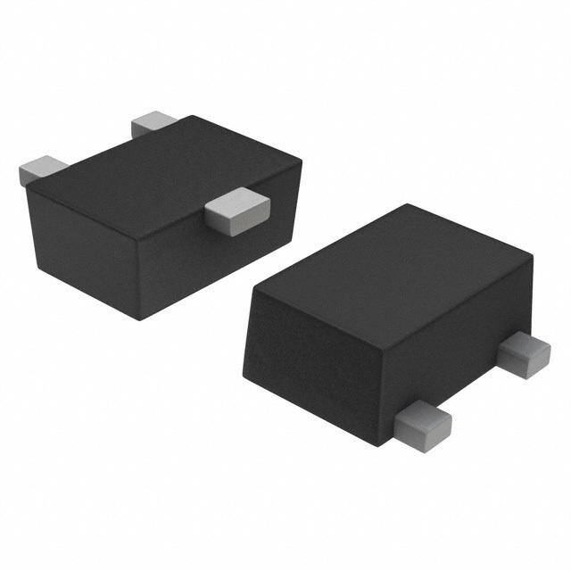
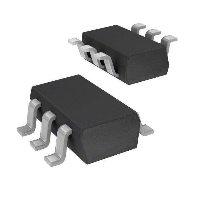
| 描述 | TVS DIODE 5VWM 13.3VC SOT723TVS 二极管 - 瞬态电压抑制器 ZEN ESD PROTECT |
| 产品分类 | |
| 品牌 | ON Semiconductor |
| 产品手册 | |
| 产品图片 |
|
| rohs | 符合RoHS无铅 / 符合限制有害物质指令(RoHS)规范要求 |
| 产品系列 | 二极管与整流器,TVS二极管,TVS 二极管 - 瞬态电压抑制器,ON Semiconductor UESD5.0DT5GuESD |
| 数据手册 | |
| 产品型号 | UESD5.0DT5G |
| PCN设计/规格 | |
| 不同频率时的电容 | 65pF @ 1MHz |
| 产品种类 | TVS 二极管 - 瞬态电压抑制器 |
| 供应商器件封装 | SOT-723 |
| 其它名称 | UESD5.0DT5GOSDKR |
| 击穿电压 | 6.2 V |
| 功率-峰值脉冲 | 117W |
| 包装 | Digi-Reel® |
| 单向通道 | 1 |
| 双向通道 | - |
| 商标 | ON Semiconductor |
| 安装类型 | 表面贴装 |
| 安装风格 | SMD/SMT |
| 封装 | Reel |
| 封装/外壳 | SOT-723 |
| 封装/箱体 | SOD-723 |
| 尺寸 | 0.8 mm W x 1.2 mm L |
| 工作温度 | -55°C ~ 150°C (TJ) |
| 工作电压 | 5 V |
| 工厂包装数量 | 8000 |
| 应用 | 通用 |
| 最大工作温度 | + 150 C |
| 最小工作温度 | - 55 C |
| 极性 | Unidirectional |
| 标准包装 | 1 |
| 电压-击穿(最小值) | 6.2V |
| 电压-反向关态(典型值) | 5V(最小值) |
| 电压-箝位(最大值)@Ipp | 13.3V |
| 电容 | 38 pF |
| 电流-峰值脉冲(10/1000µs) | 8.8A (8/20µs) |
| 电源线路保护 | 无 |
| 端接类型 | SMD/SMT |
| 类型 | 齐纳 |
| 系列 | UESD3.3ST5G |


- 商务部:美国ITC正式对集成电路等产品启动337调查
- 曝三星4nm工艺存在良率问题 高通将骁龙8 Gen1或转产台积电
- 太阳诱电将投资9.5亿元在常州建新厂生产MLCC 预计2023年完工
- 英特尔发布欧洲新工厂建设计划 深化IDM 2.0 战略
- 台积电先进制程称霸业界 有大客户加持明年业绩稳了
- 达到5530亿美元!SIA预计今年全球半导体销售额将创下新高
- 英特尔拟将自动驾驶子公司Mobileye上市 估值或超500亿美元
- 三星加码芯片和SET,合并消费电子和移动部门,撤换高东真等 CEO
- 三星电子宣布重大人事变动 还合并消费电子和移动部门
- 海关总署:前11个月进口集成电路产品价值2.52万亿元 增长14.8%


PDF Datasheet 数据手册内容提取
(cid:2)ESD3.3DT5G SERIES ESD Protection Diodes Ultra Small SOT−723 Package The (cid:2)ESD Series is designed to protect voltage sensitive components from ESD. Excellent clamping capability, low leakage, and fast response time, make these parts ideal for ESD protection on designs where board space is at a premium. Because of its small size, it is suited for use in www.onsemi.com cellular phones, portable devices, digital cameras, power supplies and many other portable applications. PIN1.CATHODE 1 Specification Features: 2.CATHODE 3 • Small Body Outline Dimensions: 3.ANODE 2 0.047″ x 0.032″(1.20 mm x 0.80 mm) • Low Body Height: 0.020″ (0.5 mm) • Stand−off Voltage: 3.3 V − 6.0 V MARKING • Low Leakage DIAGRAM • 3 Response Time is Typically < 1 ns • ESD Rating of Class 3 (> 16 kV) per Human Body Model 2 • 1 xx M IEC61000−4−2 Level 4 ESD Protection • SOT−723 IEC61000−4−4 Level 4 EFT Protection CASE 631AA • AEC−Q101 Qualified and PPAP Capable STYLE 4 xx = Device Code • These are Pb−Free Devices M = Date Code Mechanical Characteristics: CASE: Void-free, transfer-molded, thermosetting plastic Epoxy Meets UL 94 V−0 ORDERING INFORMATION LEAD FINISH: 100% Matte Sn (Tin) Device Package Shipping† MOUNTING POSITION: Any QUALIFIED MAX REFLOW TEMPERATURE: 260°C UESDxxDT5G SOT−723 8000/Tape & Reel Device Meets MSL 1 Requirements †For information on tape and reel specifications, including part orientation and tape sizes, please refer to our Tape and Reel Packaging Specifications MAXIMUM RATINGS Brochure, BRD8011/D. Rating Symbol Value Unit IEC 61000−4−2 (ESD) Air ±30 kV Contact ±30 DEVICE MARKING INFORMATION IEC 61000−4−4 (EFT) 40 A See specific marking information in the device marking column of the table on page 2 of this data sheet. ESD Voltage Per Human Body Model 16 kV Per Machine Model 400 V Total Power Dissipation on FR−5 Board ⎪ (Note 1) @ TA = 25°C PD 240 mW Derate above 25°C 1.9 mW/°C Thermal Resistance Junction−to−Ambient R(cid:3)JA 525 °C/W Junction and Storage Temperature Range TJ, Tstg −55 to °C +150 Lead Solder Temperature − Maximum TL 260 °C (10 Second Duration) Stresses exceeding those listed in the Maximum Ratings table may damage the device. If any of these limits are exceeded, device functionality should not be assumed, damage may occur and reliability may be affected. 1. FR−5 = 1.0 x 0.75 x 0.62 in. © Semiconductor Components Industries, LLC, 2013 1 Publication Order Number: October, 2017 − Rev. 5 UESD3.3DT5G/D
(cid:2)ESD3.3DT5G SERIES ELECTRICAL CHARACTERISTICS I (TA = 25°C unless otherwise noted) Symbol Parameter IF IPP Maximum Reverse Peak Pulse Current VC Clamping Voltage @ IPP VRWM Working Peak Reverse Voltage IR Maximum Reverse Leakage Current @ VRWM VC VBRVRWM V VBR Breakdown Voltage @ IT IIRT VF IT Test Current IF Forward Current VF Forward Voltage @ IF Ppk Peak Power Dissipation IPP C Max. Capacitance @VR = 0 and f = 1 MHz Uni−Directional ELECTRICAL CHARACTERISTICS (TA = 25°C unless otherwise noted, VF = 1.1 V Max. @ IF = 10 mA for all types) VBR (V) @ IT Device VRWM (V) IR ((cid:2)A) @ VRWM (Note 2) IT C (pF) Device* Marking Max Max Min mA Typ UESD3.3DT5G L0 3.3 1.0 5.0 1.0 47 UESD5.0DT5G L2 5.0 0.1 6.2 1.0 38 UESD6.0DT5G L3 6.0 0.1 7.0 1.0 34 *Other voltages available upon request. 2. VBR is measured with a pulse test current IT at an ambient temperature of 25°C. www.onsemi.com 2
(cid:2)ESD3.3DT5G SERIES TYPICAL CHARACTERISTICS )Z 7.4 20 @ I Z 7.3 18 V S) ( 7.2 16 T 7.1 OL (cid:2)ESDxxDT5G 14 V 7.0 12 E ( 6.9 A) LTAG 6.8 (nIR 180 O 6.7 V N 6.6 6 (cid:2)ESDxxDT5G W O 6.5 4 D K 6.4 2 A RE 6.3 0 B −55 +25 +150 −55 +25 +150 TEMPERATURE (°C) TEMPERATURE (°C) Figure 1. Typical Breakdown Voltage Figure 2. Typical Leakage Current versus Temperature versus Temperature 45 300 40 W) m250 CE (pF) 3305 (cid:2)ESDxxDT5G PATION (200 N 25 SI A S150 ACIT 20 R DI AP 15 WE100 C O FR−5 BOARD 10 P , D 50 5 P 0 0 0 1 2 3 4 5 0 25 50 75 100 125 150 175 BIAS VOLTAGE (V) TEMPERATURE (°C) Figure 3. Typical Capacitance versus Bias Voltage Figure 4. Steady State Power Derating Curve Figure 5. Positive 8 kV contact per IEC 6100−4−2 Figure 6. Negative 8 kV contact per IEC 61000−4−2 − (cid:2)ESD5.0DT5G − (cid:2)ESD5.0DT5G www.onsemi.com 3
(cid:2)ESD3.3DT5G SERIES PACKAGE DIMENSIONS SOT−723 CASE 631AA ISSUE D −X− NOTES: 1. DIMENSIONING AND TOLERANCING PER ASME D Y14.5M, 1994. b1 A 2. CONTROLLING DIMENSION: MILLIMETERS. 3 −Y− 3. MAXIMUM LEAD THICKNESS INCLUDES LEAD FINISH. MINIMUM LEAD THICKNESS IS THE MINIMUM THICKNESS OF BASE MATERIAL. E HE 4. DIMENSIONS D AND E DO NOT INCLUDE MOLD FLASH, PROTRUSIONS OR GATE BURRS. 1 2 2X e 2Xb0.08 X Y C DAIM M0.I4NM5ILLNI0MO.5EM0TERSM0.A55X SIDE VIEW b 0.15 0.21 0.27 TOP VIEW b1 0.25 0.31 0.37 C 0.07 0.12 0.17 3XL D 1.15 1.20 1.25 1 E 0.75 0.80 0.85 e 0.40 BSC HE 1.15 1.20 1.25 L 0.29 REF L2 0.15 0.20 0.25 STYLE 4: 3XL2 PIN 1.CATHODE 2.CATHODE BOTTOM VIEW 3.ANODE RECOMMENDED SOLDERING FOOTPRINT* 2X 0.40 2X 0.27 PACKAGE OUTLINE 1.50 3X 0.52 0.36 DIMENSIONS: MILLIMETERS *For additional information on our Pb−Free strategy and soldering details, please download the ON Semiconductor Soldering and Mounting Techniques Reference Manual, SOLDERRM/D. ON Semiconductor and are trademarks of Semiconductor Components Industries, LLC dba ON Semiconductor or its subsidiaries in the United States and/or other countries. ON Semiconductor owns the rights to a number of patents, trademarks, copyrights, trade secrets, and other intellectual property. A listing of ON Semiconductor’s product/patent coverage may be accessed at www.onsemi.com/site/pdf/Patent−Marking.pdf. ON Semiconductor reserves the right to make changes without further notice to any products herein. ON Semiconductor makes no warranty, representation or guarantee regarding the suitability of its products for any particular purpose, nor does ON Semiconductor assume any liability arising out of the application or use of any product or circuit, and specifically disclaims any and all liability, including without limitation special, consequential or incidental damages. Buyer is responsible for its products and applications using ON Semiconductor products, including compliance with all laws, regulations and safety requirements or standards, regardless of any support or applications information provided by ON Semiconductor. “Typical” parameters which may be provided in ON Semiconductor data sheets and/or specifications can and do vary in different applications and actual performance may vary over time. All operating parameters, including “Typicals” must be validated for each customer application by customer’s technical experts. ON Semiconductor does not convey any license under its patent rights nor the rights of others. ON Semiconductor products are not designed, intended, or authorized for use as a critical component in life support systems or any FDA Class 3 medical devices or medical devices with a same or similar classification in a foreign jurisdiction or any devices intended for implantation in the human body. Should Buyer purchase or use ON Semiconductor products for any such unintended or unauthorized application, Buyer shall indemnify and hold ON Semiconductor and its officers, employees, subsidiaries, affiliates, and distributors harmless against all claims, costs, damages, and expenses, and reasonable attorney fees arising out of, directly or indirectly, any claim of personal injury or death associated with such unintended or unauthorized use, even if such claim alleges that ON Semiconductor was negligent regarding the design or manufacture of the part. ON Semiconductor is an Equal Opportunity/Affirmative Action Employer. This literature is subject to all applicable copyright laws and is not for resale in any manner. PUBLICATION ORDERING INFORMATION LITERATURE FULFILLMENT: N. American Technical Support: 800−282−9855 Toll Free ON Semiconductor Website: www.onsemi.com Literature Distribution Center for ON Semiconductor USA/Canada 19521 E. 32nd Pkwy, Aurora, Colorado 80011 USA Europe, Middle East and Africa Technical Support: Order Literature: http://www.onsemi.com/orderlit Phone: 303−675−2175 or 800−344−3860 Toll Free USA/Canada Phone: 421 33 790 2910 Fax: 303−675−2176 or 800−344−3867 Toll Free USA/Canada Japan Customer Focus Center For additional information, please contact your local Email: orderlit@onsemi.com Phone: 81−3−5817−1050 Sales Representative ◊ www.onsemi.com UESD3.3DT5G/D 4