ICGOO在线商城 > 集成电路(IC) > PMIC - 电源管理 - 专用 > UCD3020RGZT
 Datasheet下载
- 型号: UCD3020RGZT
- 制造商: Texas Instruments
- 库位|库存: xxxx|xxxx
- 要求:
| 数量阶梯 | 香港交货 | 国内含税 |
| +xxxx | $xxxx | ¥xxxx |
查看当月历史价格
查看今年历史价格
UCD3020RGZT产品简介:
ICGOO电子元器件商城为您提供UCD3020RGZT由Texas Instruments设计生产,在icgoo商城现货销售,并且可以通过原厂、代理商等渠道进行代购。 UCD3020RGZT价格参考。Texas InstrumentsUCD3020RGZT封装/规格:PMIC - 电源管理 - 专用, Special Purpose PMIC 48-VQFN (7x7)。您可以下载UCD3020RGZT参考资料、Datasheet数据手册功能说明书,资料中有UCD3020RGZT 详细功能的应用电路图电压和使用方法及教程。
| 参数 | 数值 |
| 产品目录 | 集成电路 (IC)半导体 |
| 描述 | IC DGTL PWR CTRLR 48VQFN专业电源管理 Fully Programmable Dig Pwr Controller |
| 产品分类 | |
| 品牌 | Texas Instruments |
| 产品手册 | |
| 产品图片 |
|
| rohs | 符合RoHS无铅 / 符合限制有害物质指令(RoHS)规范要求 |
| 产品系列 | 电源管理 IC,专业电源管理,Texas Instruments UCD3020RGZTFusion Digital Power™ |
| 数据手册 | |
| 产品型号 | UCD3020RGZT |
| 产品 | Digital Power Controllers |
| 产品目录页面 | |
| 产品种类 | 专业电源管理 |
| 供应商器件封装 | 48-VQFN(7x7) |
| 其它名称 | 296-25747-1 |
| 包装 | 剪切带 (CT) |
| 商标 | Texas Instruments |
| 安装类型 | 表面贴装 |
| 安装风格 | SMD/SMT |
| 封装 | Reel |
| 封装/外壳 | 48-VFQFN 裸露焊盘 |
| 封装/箱体 | VQFN-48 |
| 工作温度 | -40°C ~ 125°C |
| 工作温度范围 | - 40 C to + 125 C |
| 工厂包装数量 | 250 |
| 应用 | |
| 标准包装 | 1 |
| 电压-电源 | 3 V ~ 3.6 V |
| 电流-电源 | 60mA |
| 电源电压 | 3.3 V |
| 电源电流 | 60 mA |
| 类型 | Voltage Mode PWM Controllers |
| 系列 | UCD3020 |
| 输入电压范围 | 3 V to 3.6 V |
| 输入电流 | 60 mA |


- 商务部:美国ITC正式对集成电路等产品启动337调查
- 曝三星4nm工艺存在良率问题 高通将骁龙8 Gen1或转产台积电
- 太阳诱电将投资9.5亿元在常州建新厂生产MLCC 预计2023年完工
- 英特尔发布欧洲新工厂建设计划 深化IDM 2.0 战略
- 台积电先进制程称霸业界 有大客户加持明年业绩稳了
- 达到5530亿美元!SIA预计今年全球半导体销售额将创下新高
- 英特尔拟将自动驾驶子公司Mobileye上市 估值或超500亿美元
- 三星加码芯片和SET,合并消费电子和移动部门,撤换高东真等 CEO
- 三星电子宣布重大人事变动 还合并消费电子和移动部门
- 海关总署:前11个月进口集成电路产品价值2.52万亿元 增长14.8%


PDF Datasheet 数据手册内容提取
UCD3040 UCD3028 UCD3020 www.ti.com SLUS868H–DECEMBER2009–REVISEDOCTOBER2013 Digital Power Controllers CheckforSamples:UCD3040,UCD3028,UCD3020 FEATURES • ConfigurableforVoltage-Mode,Average- 1 Current-Mode,andResonant-ModeControl • DigitalControlofuptoFourVoltageFeedback 23 Loops • AllowsSynchronizationofDPWMWaveforms BetweenMultipleUCD3040,UCD3020and • UptoEightHigh-ResolutionDigitalPulsewidth UCD3028(UCD30xx)Devices Modulated(DPWM)OutputsforSupportinga WideRangeofOffline,IsolatedandNon- • AdjustableDPWMPulseWidthEnables IsolatedDC-to-DCTopologies SupportforCurrentBalancinginaMultiphase Application. – 250-psDPWMPulse-WidthResolution • High-Performance31.25-MHz,32-BitARM7 – 4-nsDPWMFrequencyResolution Processor – AdjustablePhaseShiftBetweenDPWM • 32-KByteProgramFlashand2-KByteData Outputs FlashMemoryWithErrorCorrectionCode – AdjustableDeadBandBetweenEach (ECC) DPWMPair • 4-KByteDataRAM – Active-Highor-LowDPWMPolarity • 4-KByteBootROM – Upto2-MHzDPWMSwitchingFrequency • CommunicationPeripherals • DedicatedHigh-SpeedErrorAnalog-to-Digital – PMBus Converter(EADC)forEachFeedbackLoop WithSenseResolutionofupto1mV – UART • On-Chip10-BitDandAConverter(DAC)for – SPI SettingEADCReferenceVoltage – JTAG(NotAvailableintheUCD3028) • DedicatedHardwareAcceleratedDigital • Single-SupplySolution:InternalRegulator CompensatorsorControlLawAccelerators ControlsExternalPassElement (CLA) • InternalTemperatureSensor – Three-Pole,Three-ZeroConfigurable • UptoFiveAdditionalTimers Compensator • Built-InWatchdog,BOD,andPOR – FeaturesNon-LinearDigitalControl • 80-PinQFP(PFC),64-PinQFN(RGC),48-Pin – MultipleProgrammableCoefficient QFN(RGZ),and40-PinQFN(RHAandRMH) RegistersforAdaptiveDigital PackageOfferings Compensation • OperatingTemperatureRange: –40°Cto125°C • Upto15-Channel,12-Bit,200-ksps,Analog-to- DigitalConverter(ADC) APPLICATIONS • MultipleLevelsofFaultProtection • IsolatedAC-to-DCandDC-to-DCPower – FourHigh-SpeedAnalogComparators Supplies – ExternalFaultInputs • Power-FactorCorrection – 12-BitADC • Non-IsolatedDC-to-DCPowerSupplies 1 Pleasebeawarethatanimportantnoticeconcerningavailability,standardwarranty,anduseincriticalapplicationsof TexasInstrumentssemiconductorproductsanddisclaimerstheretoappearsattheendofthisdatasheet. FusionDigitalPower,CodeComposerStudioaretrademarksofTexasInstruments. 2 Allothertrademarksarethepropertyoftheirrespectiveowners. 3 PRODUCTIONDATAinformationiscurrentasofpublicationdate. Copyright©2009–2013,TexasInstrumentsIncorporated Products conform to specifications per the terms of the Texas Instruments standard warranty. Production processing does not necessarilyincludetestingofallparameters.
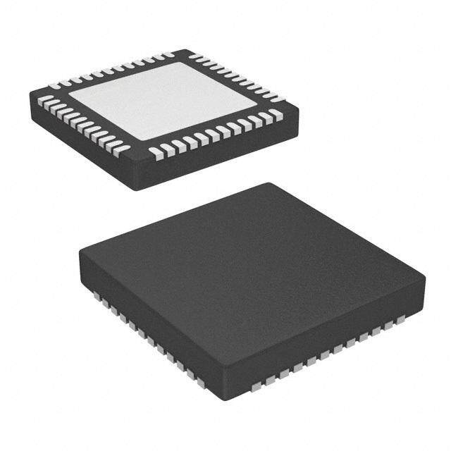
UCD3040 UCD3028 UCD3020 SLUS868H–DECEMBER2009–REVISEDOCTOBER2013 www.ti.com This integrated circuit can be damaged by ESD. Texas Instruments recommends that all integrated circuits be handled with appropriateprecautions.Failuretoobserveproperhandlingandinstallationprocedurescancausedamage. ESDdamagecanrangefromsubtleperformancedegradationtocompletedevicefailure.Precisionintegratedcircuitsmaybemore susceptibletodamagebecauseverysmallparametricchangescouldcausethedevicenottomeetitspublishedspecifications. DESCRIPTION The UCD30xx devices are members of a family of digital PWM controllers from Texas Instruments providing a single-chip control solution for digital power-conversion applications. These devices allow digital control implementation of a high-performance, high-frequency power supply with flexible configuration of parameters, supervisory,monitoring,andcommunicationfunctions. The UCD30xx are fully programmable solutions that are configurable to support a wide range of isolated and non-isolated topologies in single- or multiphase configurations. Some examples include interleaved PFC, isolated forward,half-bridge,phase-shiftedfullbridge,activeclamp,andresonantLLC. At the core of the UCD30xx controllers are the digital control-loop peripherals, also known as Fusion Digital Power™ peripherals (FDPP). Each FDPP implements a high-speed digital control loop consisting of a dedicated error analog-to-digital converter (EADC), a three-pole/three-zero (3p, 3z) digital compensator, and two DPWM outputs with 250-ps pulse-width resolution. The device also contains a 12-bit, 200-ksps general-purpose ADC with up to 15 channels, timers, interrupt controls, and communications ports such as PMBus, SCI, and SPI. The device is based on a 32-bit ARM7 RISC CPU that performs real-time monitoring, configures peripherals, and managescommunications.TheCPUexecutesitsprogramoutofprogrammableflashmemoryaswellasROM. TheUCD30xxissupportedbyTexasInstruments'CodeComposerStudio™softwaredevelopmentenvironment. ORDERINGINFORMATION OPERATING ORDERABLEPART TOP-SIDE TEMPERATURE PINCOUNT SUPPLY PACKAGE NUMBER MARKING RANGE,T A UCD3028RHAR 40 Reelof2500 QFN UCD3028 UCD3028RHAT 40 Reelof250 QFN UCD3028 UCD3028RMHR 40 Reelof2500 QFN 3028RMH UCD3028RMHT 40 Reelof250 QFN 3028RMH UCD3020RGZR 48 Reelof2500 QFN UCD3020 –40°Cto125°C UCD3020RGZT 48 Reelof250 QFN UCD3020 UCD3040RGCR 64 Reelof2000 QFN UCD3040 UCD3040RGCT 64 Reelof250 QFN UCD3040 UCD3040PFCR 80 Reelof1000 QFP UCD3040 UCD3040PFC 80 Trayof119 QFP UCD3040 2 SubmitDocumentationFeedback Copyright©2009–2013,TexasInstrumentsIncorporated ProductFolderLinks:UCD3040UCD3028UCD3020
UCD3040 UCD3028 UCD3020 www.ti.com SLUS868H–DECEMBER2009–REVISEDOCTOBER2013 PRODUCT SELECTION MATRIX UCD3040 UCD3040 UCD3020 UDC3028 UDC3028 FEATURE PFC RGC RGZ RHA RMH Package Package Package Package Package ARM7coreprocessor 31.25MHz 31.25MHz 31.25MHz 31.25MHz 31.25MHz High-resolutionDPWMoutputs(250-psresolution) 8 8 6 8 8 Numberofhigh-speedindependentfeedbackloops(number 4 4 2 2 2 ofregulatedoutputvoltages) 12-bit,200-ksps,general-purposeADCchannels 15 11 9 9 9 DigitalcomparatorsatADCoutputs 6 6 6 6 6 Flashmemory(program) 32KB 32KB 32KB 32KB 32KB Flashmemory(data) 2KB 2KB 2KB 2KB 2KB Flashsecurity √ √ √ √ √ RAM 4KB 4KB 4KB 4KB 4KB DPWMswitchingfrequency Upto2MHz Upto2MHz Upto2MHz Upto2MHz Upto2MHz Programmablefaultinputs 8 8 6 2 2 High-speedanalogcomparators 4 4 4 4 4 UART(SCI) 1 1 1 1(1) 1(1) PMBus √ √ √ √ √ Timers 4(16-bit)and 4(16-bit) 4(16-bit)and 4(16-bit)and 4(16-bit)and 1(24-bit) and 1(24-bit) 1(24-bit) 1(24-bit) 1(24-bit) TimerPWMoutputs 4 4 2 2 2 Timercompareoutputs 1 1(2) 1(2) 0 0 Timercaptureinputs 2 2(2) 2(2) 0 0 Watchdog √ √ √ √ √ On-chiposcillator √ √ √ √ √ Power-onresetandbrownoutreset √ √ √ √ √ JTAG √ √ √ Packageoffering 80-pinQFP 64-pinQFN 48-pinQFN 40-pinQFN 40-pinQFN (14mm×14 (9mm×9 (7mm×7 (6mm×6 (6mm×6 mm) mm) mm) mm) mm) On-chipvoltage-regulatorcontrol(external-passelement) √ √ √ √ √ SyncINandsyncOUTfunctions √ √(2) √(2) √(1) √(1) TotalGPIO(includesallpinswithmultiplexedfunctions,such 33 26 21 20 20 asDPWM,faultinputs,SCI,SPI,etc.) ExternalVreffor12-bitADC √ √ Externalinterrupts 2 2(2) 2(2) SPI 1 1(1) 1(1) (1) MultiplexedpinswithSYNC_IN,SYNC_OUT,andSCI (2) MultiplexedpinswithJTAG Copyright©2009–2013,TexasInstrumentsIncorporated SubmitDocumentationFeedback 3 ProductFolderLinks:UCD3040UCD3028UCD3020
UCD3040 UCD3028 UCD3020 SLUS868H–DECEMBER2009–REVISEDOCTOBER2013 www.ti.com FUNCTIONAL BLOCK DIAGRAMS UCD3040 80 Pin Compensator GPIO_06/DPWM-4A EAP4 Digital GPIO_07/DPWM-4B ErrorADC 3P–3Z High Res GPIO_32/FAULT-4A EAN4 PWM4 GPIO_33/FAULT-4B Compensator GPIO_04/DPWM-3A EAP3 Digital GPIO_05/DPWM-3B ErrorADC 3P–3Z High Res GPIO_30/FAULT-3A EAN3 PWM3 GPIO_31/FAULT-3B Compensator GPIO_02/DPWM-2A EAP2 Digital GPIO_03/DPWM-2B ErrorADC 3P–3Z High Res GPIO_10/FAULT-2A EAN2 PWM2 GPIO_11/FAULT-2B ErrorADC Compensator GPIO_00/DPWM-1A EAP1 Diff – ADC Digital GPIO_01/DPWM-1B EA 3P–3Z High Res Amp 6 Bit GPIO_08/FAULT-1A EAN1 Ref + PWM1 GPIO_09/FAULT-1B Coeff Regs Fusion Digital Power GPIO_28/SYNC-IN Peripheral GPIO_29/SYNC-OUT 4 PWR 5 GND Internal AD-00/PMB_ADDR1 Temp Sense AD-01/PMB_ADDR2 Capture GPIO_34/TCAP0 AD-02|COMP1 AD-02 + Timers and GPIO_35/TCAP1 AD-03|COMP2 TRIP1 Compare GPIO_36/TCOMPARE AD-04|COMP3 Ref1 – AD-05|COMP4 GPIO_18/PWM1 AD•••-08 ••• 201A02D kBCsipts ADR-e0f32 –+ TRIP2 RIBASaRCsM Ce7dPU Watchdog PWM GGGPPPIIIOOO___122901///PPPWWWMMM234 AD-09 AD-10 AD-04 + TRIP3 Comms AD-11 Ref3 – AD-12 PMBUS-CLK AD-13 PMBUS-DATA AD-14 AD-05 + PMBus PMBUS-ALERT TRIP4 PMBUS-CNTL Ref4 – ADCREFIN/EXTREF GPIO_16/SCI-TX UART V33FB Internal Analog Comparators GPIO_17/SCI-RX GND 3.3 V and 1.8 V GPIO_22/SPI-CLK BPCAP Control Flash SPI GPIO_26/SPI-CS 1.8 V Memory GPIO_24/SPI-DI Regulator With ECC GPIO_23/SPI-DO Prog: 32KB TRST Data: 2KB TMS Osc RAM: 4KB GPIO_25/INT1 Device TDI System GPIO_27/INT2 Support TDO JTAG POR/BOD RESET TCK RET_CLK B0376-04 4 SubmitDocumentationFeedback Copyright©2009–2013,TexasInstrumentsIncorporated ProductFolderLinks:UCD3040UCD3028UCD3020
UCD3040 UCD3028 UCD3020 www.ti.com SLUS868H–DECEMBER2009–REVISEDOCTOBER2013 UCD3040 64 Pin Compensator GPIO_06/DPWM-4A EAP4 Digital GPIO_07/DPWM-4B ErrorADC 3P–3Z High Res GPIO_32/FAULT-4A EAN4 PWM4 GPIO_33/FAULT-4B Compensator GPIO_04/DPWM-3A EAP3 Digital GPIO_05/DPWM-3B ErrorADC 3P–3Z High Res GPIO_30/FAULT-3A EAN3 PWM3 GPIO_31/FAULT-3B Compensator GPIO_02/DPWM-2A EAP2 Digital GPIO_03/DPWM-2B ErrorADC 3P–3Z High Res GPIO_10/FAULT-2A EAN2 PWM2 GPIO_11/FAULT-2B ErrorADC Compensator GPIO_00/DPWM-1A EAP1 Diff – ADC Digital GPIO_01/DPWM-1B EA 3P–3Z High Res Amp 6 Bit GPIO_08/FAULT-1A EAN1 Ref + PWM1 GPIO_09/FAULT-1B Coeff Regs Fusion Digital Power Peripheral 4 PWR 5 GND Internal SPI AD-00/PMB_ADDR1 Temp Sense Timers AD-01/PMB_ADDR2 GPIO_18/PWM1 AD-02|COMP1 AD-02 + GPIO_19/PWM2 AD-03|COMP2 TRIP1 Watchdog PWM AD-04|COMP3 ADC Ref1 – GPIO_20/PWM3 GPIO_21/PWM4 AD-05|COMP4 12 Bit • • 200 ksps AD-03 + •• •• TRIP2 ARM7 AD-08 Ref2 – RIBSaCs CedPU AD-09 PMBUS-CLK AD-10 AD-04 + PMBUS-DATA PMBus TRIP3 PMBUS-ALERT Ref3 – PMBUS-CNTL AD-05 + TRIP4 Ref4 – GPIO_16/SCI-TX UART GPIO_17/SCI-RX V33FB Internal Analog Comparators GND 3.3 V and 1.8 V BPCAP Control Flash Re1g.u8l aVtor WMitehm EoCryC System RESET Prog: 32KB TRST TTMDSI//FFUUNNCC22((11)) SDuepvpicoert Osc RDAatMa:: 24KKBB SPI JTAG TDO/FUNC2(1) Multiplexed POR/BOD TCK/FUNC2(1) Sync In/Out RET_CLK B0376-03 (1) FUNC2forthefourpinsTMS,TDI,TDO,andTCKindicatessecondaryfunctionsavailableonthesepins.Theseare configurablebytheIO_FUNC_MODEbitsintheI/OFunctionalMultiplexerControlregister(IOMUXCTRL). Copyright©2009–2013,TexasInstrumentsIncorporated SubmitDocumentationFeedback 5 ProductFolderLinks:UCD3040UCD3028UCD3020
UCD3040 UCD3028 UCD3020 SLUS868H–DECEMBER2009–REVISEDOCTOBER2013 www.ti.com UCD3020 48 Pin GPIO_06/DPWM-4A Digital GPIO_07/DPWM-4B High Res GPIO_32/FAULT-4A PWM4 GPIO_33/FAULT-4B Compensator GPIO_02/DPWM-2A EAP2 Digital GPIO_03/DPWM-2B ErrorADC 3P–3Z High Res GPIO_10/FAULT-2A EAN2 PWM2 GPIO_11/FAULT-2B ErrorADC Compensator GPIO_00/DPWM-1A EAP1 Diff – ADC Digital GPIO_01/DPWM-1B EA 3P–3Z High Res Amp 6 Bit GPIO_08/FAULT-1A EAN1 Ref + PWM1 GPIO_09/FAULT-1B Coeff Regs Fusion Digital Power 2 Peripheral PWR 2 GND Internal AD-00/PMB_ADDR1 Temp Sense AD-01/PMB_ADDR2 GPIO GPIO30 AD-02|COMP1 AD-02 + AD-03|COMP2 TRIP1 AD-04|COMP3 ADC Ref1 – Timer GPIO_18/PWM1 AD-05|COMP4 12 Bit PWM GPIO_19/PWM2 AD-06 200 ksps AD-03 + AD-07 TRIP2 ARM7 AD-08 Ref2 – Based RISC CPU TRST ADCREFIN/ExtRef AD-04 + TRIP3 SDuepvpicoert TTMDOS//FFUUNNCC22((11)) Ref3 – TDI/FUNC2(1) TCK/FUNC2(1) AD-05 + TRIP4 Ref4 – V33FB Internal Analog Comparators SPI GND 3.3 V and 1.8 V BPCAP Control Flash Re1g.u8l aVtor WMitehm EoCryC SCI GGPPIIOO__1167//SSCCII--TRXX Prog: 32KB Data: 2KB Osc RAM: 4KB PMBUS-CLK POR/BOD PMBUS-DATA PMBus PMBUS-ALERT PMBUS-CNTL System RESET B0376-01 (1) FUNC2forthefourpinsTMS,TDI,TDO,andTCKindicatessecondaryfunctionsavailableonthesepins.Theseare configurablethebyIO_FUNC_MODEbitsintheI/OFunctionalMultiplexerControlregister(IOMUXCTRL). 6 SubmitDocumentationFeedback Copyright©2009–2013,TexasInstrumentsIncorporated ProductFolderLinks:UCD3040UCD3028UCD3020
UCD3040 UCD3028 UCD3020 www.ti.com SLUS868H–DECEMBER2009–REVISEDOCTOBER2013 UCD3028 40 Pin Digital GPIO_06/DPWM-4A High Res GPIO_07/DPWM-4B PWM4 Digital GPIO_04/DPWM-3A High Res GPIO_05/DPWM-3B PWM3 Compensator EAP2 Digital GPIO_02/DPWM-2A ErrorADC 3P–3Z High Res GPIO_03/DPWM-2B EAN2 PWM2 GPIO_10/FAULT-2A ErrorADC Compensator GPIO_00/DPWM-1A EAP1 Diff – ADC Digital GPIO_01/DPWM-1B EA 3P–3Z High Res Amp 6 Bit GPIO_08/FAULT-1A EAN1 Ref + PWM1 Coeff Regs 2 PWR 2 GND Internal AD-00/PMB_ADDR1 Temp Sense Timer GPIO_18/PWM1 AD-01/PMB_ADDR2 PWM GPIO_19/PWM2 AD-02 AD-02 + AD-03 ADC TRIP1 AD-04 12 Bit Ref1 – SCI AD-05 200 ksps Multiplexed SCI_TX/SYNC_OUT(1) AD-06 AD-03 + ARM7 SYNC_IN/ SCI_RX/SYNC_IN(1) AD-07 TRIP2 Based OUT SYNC_IN(1) AD-08 Ref2 – RISC CPU AD-04 + TRIP3 PMBUS-CLK GND Internal Ref3 – PMBUS-DATA 3.3 V and 1.8 V PMBus BPCAP Control PMBUS-ALERT AD-05 + PMBUS-CNTL TRIP4 Ref4 – RESET Re1g.u8l aVtor Analog Comparators Flash System TEST Memory With ECC Osc Prog: 32KB Data: 2KB RAM: 4KB POR/BOD B0376-02 (1) RequiresconfigurationofIO_FUNC_MODEbitsintheI/Ofunctionalmultiplexercontrolregister(IOMUXCTRL) Copyright©2009–2013,TexasInstrumentsIncorporated SubmitDocumentationFeedback 7 ProductFolderLinks:UCD3040UCD3028UCD3020
UCD3040 UCD3028 UCD3020 SLUS868H–DECEMBER2009–REVISEDOCTOBER2013 www.ti.com UCD3040 Pin Assignments PFC Package (Top View) 12 RR DD DD AA1 __P BBM MMO PPC GNDD-06D-07D-00/D-01/D-02|D-11D-12D-13D-1433FBAN4AP4AN3AP3AN2AP2AN1AP1GND AAAAAAAAAAVEEEEEEEEA 8079787776757473727170696867666564636261 ADCREFIN/EXTREF 1 60 AGND AD-05|COMP4 2 59 BPCAP AD-04|COMP3 3 58 V33A AD-03|COMP2 4 57 V33D AD-08 5 56 V33DIO AD-09 6 55 DGND AD-10 7 54 GPIO_20/PWM3 V33DIO 8 53 GPIO_21/PWM4 DGND 9 52 GPIO_22/SPI-CLK GPIO_36/TCOMPARE 10 51 GPIO_23/SPI-DO GPIO_35/TCAP1 11 50 GPIO_24/SPI-DI GPIO_34/TCAP0 12 49 GPIO_25/INT1 RESET 13 48 TRST RET_CLK 14 47 TMS GPIO_08/FAULT-1A 15 46 TDI GPIO_09/FAULT-1B 16 45 TDO GPIO_10/FAULT-2A 17 44 TCK GPIO_11/FAULT-2B 18 43 GPIO_33/FAULT-4B PMBUS-CLK 19 42 GPIO_32/FAULT-4A PMBUS-DATA 20 41 GPIO_31/FAULT-3B 12345678901234567890 22222222233333333334 GPIO_00/DPWM-1AGPIO_01/DPWM-1BGPIO_02/DPWM-2AGPIO_03/DPWM-2BGPIO_04/DPWM-3AGPIO_05/DPWM-3BGPIO_06/DPWM-4AGPIO_07/DPWM-4BGPIO_30/FAULT-3APIO_29/SYNC-OUTGPIO_28/SYNC-INGPIO_27/INT2GPIO_26/SPI-CSDGNDPMBUS-ALERTPMBUS-CNTLGPIO_16/SCI-TXGPIO_17/SCI-RXGPIO_18/PWM1GPIO_19/PWM2 G 8 SubmitDocumentationFeedback Copyright©2009–2013,TexasInstrumentsIncorporated ProductFolderLinks:UCD3040UCD3028UCD3020
UCD3040 UCD3028 UCD3020 www.ti.com SLUS868H–DECEMBER2009–REVISEDOCTOBER2013 RGC Package (Top View) 1 2 R R D D D D A A 1 _ _ P B B M M M O P P C GND D-06 D-07 D-00/ D-01/ D-02| 33FB AN4 AP4 AN3 AP3 AN2 AP2 AN1 AP1 GND A A A A A A V E E E E E E E E A 4 3 2 1 0 9 8 7 6 5 4 3 2 1 0 9 AD-05|COMP4 16 6 6 6 6 5 5 5 5 5 5 5 5 5 5 448 AGND AD-04|COMP3 2 47 BPCAP AD-03|COMP2 3 46 V33A AD-08 4 45 V33D AD-09 5 44 V33DIO AD-10 6 43 DGND V33DIO 7 42 GPIO_20/PWM3 DGND 8 41 GPIO_21/PWM4 Thermal Pad RESET 9 40 TRST (1) RET_CLK 10 39 TMS/FUNC2 GPIO_08/FAULT-1A 11 38 TDI/FUNC2(1) GPIO_09/FAULT-1B 12 37 TDO/FUNC2(1) GPIO_10/FAULT-2A 13 36 TCK/FUNC2(1) GPIO_11/FAULT-2B 14 35 GPIO_33/FAULT-4B PMBUS-CLK 15 34 GPIO_32/FAULT-4A PMBUS-DATA 16 33 GPIO_31/FAULT-3B 7 8 9 0 1 2 3 4 5 6 7 8 9 0 1 2 1 1 1 2 2 2 2 2 2 2 2 2 2 3 3 3 1A 1B 2A 2B 3A 3B 4A 4B 3A ND RT TL TX RX M1 M2 PIO_00/DPWM- PIO_01/DPWM- PIO_02/DPWM- PIO_03/DPWM- PIO_04/DPWM- PIO_05/DPWM- PIO_06/DPWM- PIO_07/DPWM- PIO_30/FAULT- DG PMBUS-ALE PMBUS-CN GPIO_16/SCI- GPIO_17/SCI- GPIO_18/PW GPIO_19/PW G G G G G G G G G (1) FUNC2forthefourpinsTMS,TDI,TDO,andTCKindicatessecondaryfunctionsavailableonthesepins.Theseare configurablebytheIO_FUNC_MODEbitsintheI/OFunctionalMultiplexerControlregister(IOMUXCTRL). TheUCD3040isavailableinaplastic80-pinTQFPpackageanda64-pinQFN package. Copyright©2009–2013,TexasInstrumentsIncorporated SubmitDocumentationFeedback 9 ProductFolderLinks:UCD3040UCD3028UCD3020
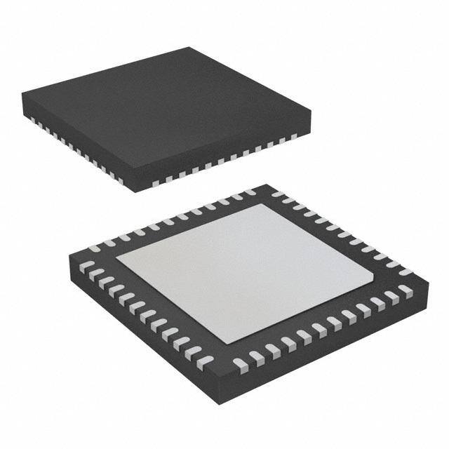
UCD3040 UCD3028 UCD3020 SLUS868H–DECEMBER2009–REVISEDOCTOBER2013 www.ti.com UCD3020 Pin Assignments RGZ Package (Top View) F 1 2 E R R R D D T D D X A A 1 E _ _ P N/ B B M EFI PM PM CO DCR GND D-06 D-07 D-00/ D-01/ D-02| 33FB AN2 AP2 AN1 AP1 A A A A A A A V E E E E 8 7 6 5 4 3 2 1 0 9 8 7 AD-05|COMP4 14 4 4 4 4 4 4 4 4 3 3 336 AGND AD-04|COMP3 2 35 BPCAP AD-03|COMP2 3 34 V33A AD-08 4 33 V33D RESET 5 32 DGND GPIO_08/FAULT-1A 6 31 TRST Thermal Pad GPIO_09/FAULT-1B 7 30 TMS/FUNC2(1) GPIO_10/FAULT-2A 8 29 TDI/FUNC2(1) GPIO_11/FAULT-2B 9 28 TDO/FUNC2(1) (1) PMBUS-CLK 10 27 TCK/FUNC2 PMBUS-DATA 11 26 GPIO_33/FAULT-4B GPIO_00/DPWM-1A 12 25 GPIO_32/FAULT-4A 3 4 5 6 7 8 9 0 1 2 3 4 1 1 1 1 1 1 1 2 2 2 2 2 1B 2A 2B 4A 4B 30 RT TL TX RX M1 M2 PIO_01/DPWM- PIO_02/DPWM- PIO_03/DPWM- PIO_06/DPWM- PIO_07/DPWM- GPIO PMBUS-ALE PMBUS-CN GPIO_16/SCI- GPIO_17/SCI- GPIO_18/PW GPIO_19/PW G G G G G (1) FUNC2forthefourpinsTMS,TDI,TDO,andTCKindicatessecondaryfunctionsavailableonthesepins.Theseare configurablebytheIO_FUNC_MODEbitsintheI/OFunctionalMultiplexerControlregister(IOMUXCTRL). TheUCD3020isavailableinaplastic48-pinQFN package. 10 SubmitDocumentationFeedback Copyright©2009–2013,TexasInstrumentsIncorporated ProductFolderLinks:UCD3040UCD3028UCD3020
UCD3040 UCD3028 UCD3020 www.ti.com SLUS868H–DECEMBER2009–REVISEDOCTOBER2013 UDC3028 Pin Assignments RHAPackage (Top View) 1 2 R R D D D D A A 1 _ _ M B B P M M O P P C GND D-06 D-07 D-00/ D-01/ D-02/ AN2 AP2 AN1 AP1 A A A A A A E E E E 40 39 38 37 36 35 34 33 32 31 AD05/COMP4 1 30 AGND AD04/COMP3 2 29 BPCAP AD03/COMP2 3 28 V33A AD08 4 27 V33D RESET 5 26 DGND Thermal Pad GPIO_08/FAULT-1A 6 25 TEST GPIO_10/FAULT-2A 7 24 SCI_RX/SYNC_IN GPIO_12/PMBUS-CLK 8 23 SCI_TX/SYNC_OUT GPIO_13/PMBUS-DATA 9 22 SYNC_IN GPIO_00/DPWM-1A 10 21 GPIO_19/PWM2 11 12 13 14 15 16 17 18 19 20 B A B A B A B T L 1 1 2 2 3 3 4 4 R T M M- M- M- M- M- M- M- LE CN W GPIO_01/DPW GPIO_02/DPW GPIO_03/DPW GPIO_04/DPW GPIO_05/DPW GPIO_06/DPW GPIO_07/DPW _14/PMBUS-A PI15/PMBUS- GPIO18/P O G PI G P0076-03 Copyright©2009–2013,TexasInstrumentsIncorporated SubmitDocumentationFeedback 11 ProductFolderLinks:UCD3040UCD3028UCD3020
UCD3040 UCD3028 UCD3020 SLUS868H–DECEMBER2009–REVISEDOCTOBER2013 www.ti.com RMH Package (Top View) 1 2 R R D D D D _A _A M1 B B P M M O P P C GND D-06 D-07 D-00/ D-01/ D-02/ AN2 AP2 AN1 AP1 A A A A A A E E E E 40 39 38 37 36 35 34 33 32 31 AD05/COMP4 1 30 AGND AD04/COMP3 2 29 BPCAP AD03/COMP2 3 28 V33A AD08 4 27 V33D RESET 5 26 DGND GPIO_08/FAULT-1A 6 25 TEST GPIO_10/FAULT-2A 7 24 SCI_RX/SYNC_IN GPIO_12/PMBUS-CLK 8 23 SCI_TX/SYNC_OUT GPIO_13/PMBUS-DATA 9 22 SYNC_IN GPIO_00/DPWM-1A 10 21 GPIO_19/PWM2 11 12 13 14 15 16 17 18 19 20 B A B A B A B T L 1 GPIO_01/DPWM-1 GPIO_02/DPWM-2 GPIO_03/DPWM-2 GPIO_04/DPWM-3 GPIO_05/DPWM-3 GPIO_06/DPWM-4 GPIO_07/DPWM-4 O_14/PMBUS-ALER GPI15/PMBUS-CNT GPIO18/PWM PI G NOTE RMHpackagehasthinnerpackageheightcomparedtoRHApackage. RMH package also adds four corner pins. These features help to improve solder joint reliability The corner anchor pins and thermal pad should be soldered for robust mechanical performanceandshouldbetiedtotheappropriategroundsignal. 12 SubmitDocumentationFeedback Copyright©2009–2013,TexasInstrumentsIncorporated ProductFolderLinks:UCD3040UCD3028UCD3020
UCD3040 UCD3028 UCD3020 www.ti.com SLUS868H–DECEMBER2009–REVISEDOCTOBER2013 PIN DESCRIPTIONS UCD3040 UCD3040 PFCPACKAGE RGCPACKAGE I/O DESCRIPTION Signal NO. Signal NO. AD-00/PMB_ADDR1 77 AD-00/PMB_ADDR1 61 I 12-bitADC,Ch0/PMBusaddresssense AD-01/PMB_ADDR2 76 AD-01/PMB_ADDR2 60 I 12-bitADC,Ch1/PMBusaddresssense AD-02|COMP1 75 AD-02|COMP1 59 I 12-bitADC,Ch2andanalogcomparator#1 AD-03|COMP2 4 AD-03|COMP2 3 I 12-bitADC,Ch3andanalogcomparator#2 AD-04|COMP3 3 AD-04|COMP3 2 I 12-bitADC,Ch4andanalogcomparator#3 AD-05|COMP4 2 AD-05|COMP4 1 I 12-bitADC,Ch5andanalogcomparator#4 AD-06 79 AD-06 63 I 12-bitADC,Ch6 AD-07 78 AD-07 62 I 12-bitADC,Ch7 AD-08 5 AD-08 4 I 12-bitADC,Ch8 AD-09 6 AD-09 5 I 12-bitADC,Ch9 AD-10 7 AD-10 6 I 12-bitADC,Ch10 AD-11 74 — — I 12-bitADC,Ch11 AD-12 73 — — I 12-bitADC,Ch12 AD-13 72 — — I 12-bitADC,Ch13 AD-14 71 — — I 12-bitADC,Ch14 ADCREFIN/EXTREF 1 — — I 12-bitADC,externalreference AGND 60 AGND 48 — Analogground AGND 61 AGND 49 — Analogground AGND 80 AGND 64 — Analogground BPCAP 59 BPCAP 47 O 1.8-Vbypasscapacitorconnectpin DGND 9 DGND 8 — Digitalground DGND 34 DGND 26 — Digitalground DGND 55 DGND 43 — Digitalground EAN1 63 EAN1 51 I Channel#1,differentialanalogvoltage,negativeinput EAN2 65 EAN2 53 I Channel#2,differentialanalogvoltage,negativeinput EAN3 67 EAN3 55 I Channel#3,differentialanalogvoltage,negativeinput EAN4 69 EAN4 57 I Channel#4,differentialanalogvoltage,negativeinput EAP1 62 EAP1 50 I Channel#1,differentialanalogvoltage,positiveinput EAP2 64 EAP2 52 I Channel#2,differentialanalogvoltage,positiveinput EAP3 66 EAP3 54 I Channel#3,differentialanalogvoltage,positiveinput EAP4 68 EAP4 56 I Channel#4,differentialanalogvoltage,positiveinput GPIO_00/DPWM-1A 21 GPIO_00/DPWM-1A 17 I/O GPIOport0/DPWM1Aoutput GPIO_01/DPWM-1B 22 GPIO_01/DPWM-1B 18 I/O GPIOport1/DPWM1Boutput GPIO_02/DPWM-2A 23 GPIO_02/DPWM-2A 19 I/O GPIOport2/DPWM2Aoutput GPIO_03/DPWM-2B 24 GPIO_03/DPWM-2B 20 I/O GPIOport3/DPWM2Boutput GPIO_04/DPWM-3A 25 GPIO_04/DPWM-3A 21 I/O GPIOport4/DPWM3Aoutput GPIO_05/DPWM-3B 26 GPIO_05/DPWM-3B 22 I/O GPIOport5/DPWM3Boutput GPIO_06/DPWM-4A 27 GPIO_06/DPWM-4A 23 I/O GPIOport6/DPWM4Aoutput GPIO_07/DPWM-4B 28 GPIO_07/DPWM-4B 24 I/O GPIOport7/DPWM4Boutput GPIO_08/FAULT-1A 15 GPIO_08/FAULT-1A 11 I/O GPIOport8/externalfaultinput1A GPIO_09/FAULT-1B 16 GPIO_09/FAULT-1B 12 I/O GPIOport9/externalfaultinput1B GPIO_10/FAULT-2A 17 GPIO_10/FAULT-2A 13 I/O GPIOport10/externalfaultinput2A GPIO_11/FAULT-2B 18 GPIO_11/FAULT-2B 14 I/O GPIOport11/externalfaultinput2B GPIO_16/SCI-TX 37 GPIO_16/SCI-TX 29 I/O GPIOport16/SCItransmit GPIO_17/SCI-RX 38 GPIO_17/SCI-RX 30 I/O GPIOport17/SCIreceive Copyright©2009–2013,TexasInstrumentsIncorporated SubmitDocumentationFeedback 13 ProductFolderLinks:UCD3040UCD3028UCD3020
UCD3040 UCD3028 UCD3020 SLUS868H–DECEMBER2009–REVISEDOCTOBER2013 www.ti.com UCD3040 UCD3040 PFCPACKAGE RGCPACKAGE I/O DESCRIPTION Signal NO. Signal NO. GPIO_19/PWM2 40 GPIO_19/PWM2 32 I/O GPIOport19/PWMoutput2(16-bittimer) GPIO_18/PWM1 39 GPIO_18/PWM1 31 I/O GPIOport18/PWMoutput1(16-bittimer) GPIO_20/PWM3 54 GPIO_20/PWM3 42 I/O GPIOport20/PWMoutput3(16-bittimer) GPIO_21/PWM4 53 GPIO_21/PWM4 41 I/O GPIOport21/PWMoutput4(16-bittimer) GPIO_22/SPI-CLK 52 — — I/O GPIOport22/SPIclock GPIO_23/SPI-DO 51 — — I/O GPIOport23/SPIdataout GPIO_24/SPI-DI 50 — — I/O GPIOport24/SPIdatain GPIO_25/INT1 49 — — I/O GPIOport25/interrupt1 GPIO_26/SPI-CS 33 — — I/O GPIOport26/SPIchipselect GPIO_27/INT2 32 — — I/O GPIOport27/interrupt2 GPIO-28/SYNC-IN 31 — — I/O GPIOport28/syncinputtoDPWM GPIO-29/SYNC-OUT 30 — — I/O GPIOport29/syncoutputfromDPWM GPIO_30/FAULT-3A 29 GPIO_30/FAULT-3A 25 I/O GPIOport30/externalfaultinput3A GPIO_31/FAULT-3B 41 GPIO_31/FAULT-3B 33 I/O GPIOport31/externalfaultinput3B GPIO_32FAULT-4A 42 GPIO_32FAULT-4A 34 I/O GPIOport32/externalfaultinput4A GPIO_33/FAULT-4B 43 GPIO_33/FAULT-4B 35 I/O GPIOport33/externalfaultinput4B GPIO_34/TCAP0 12 — — I/O GPIOport34/timercaptureinput0 GPIO_35/TCAP1 11 — — I/O GPIOport35/timercaptureinput1 GPIO_36/TCOMPARE 10 — — I/O GPIOport36/timercompareoutput PMBUS-ALERT 35 PMBUS-ALERT 27 O PMBusalert(musthavepullupto3.3V),general-purposeoutput, open-drain PMBUS-CLK 19 PMBUS-CLK 15 I/O PMBusclock(musthavepullupto3.3V) PMBUS-CNTL 36 PMBUS-CNTL 28 I PMBuscontrol,general-purposeinput PMBUS-DATA 20 PMBUS-DATA 16 I/O PMBusdata(musthavepullupto3.3V) RESET 13 RESET 9 I Active-lowdevice-resetinput RET_CLK 14 RET_CLK 10 O Returnclock TCK 44 TCK/FUNC2 36 I/O For64-pinJTAGTCKorothersecondaryfunctionsselectableby IO_FUNC_MODEbitsinI/Ofunctionalmultiplexercontrolregister.For 80-pinJTAGTCK TDI 46 TDI/FUNC2 38 I/O For64-pinJTAGTDIorothersecondaryfunctionsselectableby IO_FUNC_MODEbitsinI/Ofunctionalmultiplexercontrolregister.For 80-pinJTAGTDI TDO 45 TDO/FUNC2 37 I/O For64-pinJTAGTDOorothersecondaryfunctionsselectableby IO_FUNC_MODEbitsinI/Ofunctionalmultiplexercontrolregister.For 80-pinJTAGTDO TMS 47 TMS/FUNC2 39 I/O For64-pinJTAGTMSorothersecondaryfunctionsselectableby IO_FUNC_MODEbitsinI/Ofunctionalmultiplexercontrolregister.For 80-pinJTAGTMS TRST 48 TRST 40 I/O JTAGTRSTforboth80-pinand64-pindevices V33A 58 V33A 46 — Analog3.3-Vsupply V33D 57 V33D 45 — Digitalcore3.3-Vsupply V33DIO 8 V33DIO 7 — DigitalI/O3.3-Vsupply V33DIO 56 V33DIO 44 — DigitalI/O3.3-Vsupply V33FB 70 V33FB 58 — 3.3-Vlinear-regulatorfeedbackinput 14 SubmitDocumentationFeedback Copyright©2009–2013,TexasInstrumentsIncorporated ProductFolderLinks:UCD3040UCD3028UCD3020
UCD3040 UCD3028 UCD3020 www.ti.com SLUS868H–DECEMBER2009–REVISEDOCTOBER2013 UCD3020 RGZPACKAGE I/O DESCRIPTION Signal NO. AD-00/PMB_ADDR1 44 I 12-bitADC,Ch0/PMBusaddresssense,least-significantaddressbits AD-01/PMB_ADDR2 43 I 12-bitADC,Ch1/PMBusaddresssense,most-significantaddressbits AD-02|COMP1 42 I 12-bitADC,Ch2andanalogcomparator#1 AD-03|COMP2 3 I 12-bitADC,Ch3andanalogcomparator#2 AD-04|COMP3 2 I 12-bitADC,Ch4andanalogcomparator#3 AD-05|COMP4 1 I 12-bitADC,Ch5andanalogcomparator#4 AD-06 46 I 12-bitADC,Ch6 AD-07 45 I 12-bitADC,Ch7 AD-08 4 I 12-bitADC,Ch8 ADCREFIN/EXTREF 48 I 12-bitADC,externalreference AGND 36 — Analogground AGND 47 — Analogground BPCAP 35 O 1.8-Vbypass-capacitorconnectpin DGND 32 — Digitalground EAN1 38 I Channel#1,differentialanalogvoltage,negativeinput EAN2 40 I Channel#2,differentialanalogvoltage,negativeinput EAP1 37 I Channel#1,differentialanalogvoltage,positiveinput EAP2 39 I Channel#2,differentialanalogvoltage,positiveinput GPIO_00/DPWM-1A 12 I/O GPIOport0/DPWM1Aoutput GPIO_01/DPWM-1B 13 I/O GPIOport1/DPWM1Boutput GPIO_02/DPWM-2A 14 I/O GPIOport2/DPWM2Aoutput GPIO_03/DPWM-2B 15 I/O GPIOport3/DPWM2Boutput GPIO_06/DPWM-4A 16 I/O GPIOport6/DPWM4Aoutput GPIO_07/DPWM-4B 17 I/O GPIOport7/DPWM4Boutput GPIO_08/FAULT-1A 6 I/O GPIOport8/externalfaultinput1A GPIO_09/FAULT-1B 7 I/O GPIOport9/externalfaultinput1B GPIO_10/FAULT-2A 8 I/O GPIOport10/externalfaultinput2A GPIO_11/FAULT-2B 9 I/O GPIOport11/externalfaultinput2B GPIO_16/SCI-TX 21 I/O GPIOport16/SCItransmit GPIO_17/SCI-RX 22 I/O GPIOport17/SCIreceive GPIO_18/PWM1 23 I/O GPIOport18/PWMoutput1(16-bittimer) GPIO_19/PWM2 24 I/O GPIOport19/PWMoutput2(16-bittimer) GPIO_30 18 I/O GPIOport30 GPIO_32/FAULT-4A 25 I/O GPIOport32/externalfaultinput4A GPIO_33/FAULT-4B 26 I/O GPIOport33/externalfaultinput4B PMBUS-ALERT 19 O PMBUSalert(musthavepullupto3.3V),general-purposeoutput,open-drain PMBUS-CLK 10 I/O PMBusclock(musthavepullupto3.3V) PMBUS-CNTL 20 I PMBUScontrol,general-purposeinput PMBUS-DATA 11 I/O PMBusdata(musthavepullupto3.3V) RESET 5 I Active-lowdevice-resetinput Copyright©2009–2013,TexasInstrumentsIncorporated SubmitDocumentationFeedback 15 ProductFolderLinks:UCD3040UCD3028UCD3020
UCD3040 UCD3028 UCD3020 SLUS868H–DECEMBER2009–REVISEDOCTOBER2013 www.ti.com UCD3020 RGZPACKAGE I/O DESCRIPTION Signal NO. TCK/FUNC2 27 I/O JTAGTCKorsecondaryfunctionsselectablebyIO_FUNC_MODEbitsinI/Ofunctionalmultiplexer controlregister TDI/FUNC2 29 I/O JTAGTDIorsecondaryfunctionsselectablebyIO_FUNC_MODEbitsinI/Ofunctionalmultiplexer controlregister TDO/FUNC2 28 I/O JTAGTDOorsecondaryfunctionsselectablebyIO_FUNC_MODEbitsinI/Ofunctionalmultiplexer controlregister TMS/FUNC2 30 I/O JTAGTMSorsecondaryfunctionsselectablebyIO_FUNC_MODEbitsinI/Ofunctionalmultiplexer controlregister TRST 31 I JTAGreset V33A 34 — Analog3.3-Vsupply V33D 33 — Digitalcore3.3-Vsupply V33FB 41 — 3.3-Vlinear-regulatorfeedbackinput 16 SubmitDocumentationFeedback Copyright©2009–2013,TexasInstrumentsIncorporated ProductFolderLinks:UCD3040UCD3028UCD3020
UCD3040 UCD3028 UCD3020 www.ti.com SLUS868H–DECEMBER2009–REVISEDOCTOBER2013 UCD3028 RHAandRMHPackage I/O DESCRIPTION Signal NO. AD-00/PMB_ADDR1 37 I ADC12,Ch0/PMBusaddresssense,most-significantaddressbits AD-01/PMB_ADDR2 36 I ADC12,Ch1/PMBusaddresssense,least-significantaddressbits AD-02/COMP1 35 I ADC12,Ch2/analogcomparator#1 AD-03/COMP2 3 I ADC12,Ch3/analogcomparator#2 AD-04/COMP3 2 I ADC12,Ch4/analogcomparator#3 AD-05/COMP4 1 I ADC12,Ch5/analogcomparator#4 AD-06 39 I ADC12,Ch6 AD-07 38 I ADC12,Ch7 AD-08 4 I ADC12,Ch8 AGND 30 – Analogground AGND 40 – Analogground BPCAP 29 O 1.8-Vbypasscapacitorconnectpin DGND 26 – Digitalground EAN1 32 I Channel#1,differentialanalogerrorvoltage,negativeinput EAN2 34 I Channel#2,differentialanalogerrorvoltage,negativeinput EAP1 31 I Channel#1,differentialanalogerrorvoltage,positiveinput EAP2 33 I Channel#2,differentialanalogerrorvoltage,positiveinput GPIO_00/DPWM-1A 10 I/O GPIOport0/DPWM1Aoutput GPIO_01/DPWM-1B 11 I/O GPIOport1/DPWM1Boutput GPIO_02/DPWM-2A 12 I/O GPIOport2/DPWM2Aoutput GPIO_03/DPWM-2B 13 I/O GPIOport3/DPWM2Boutput GPIO_04/DPWM-3A 14 I/O GPIOport4/DPWM3Aoutput GPIO_05/DPWM-3B 15 I/O GPIOport5/DPWM3Boutput GPIO_06/DPWM-4A 16 I/O GPIOport6/DPWM4Aoutput GPIO_07/DPWM-4B 17 I/O GPIOport7/DPWM4Boutput GPIO_08/FAULT-1A 6 I/O GPIOport8/externalfaultinput1A GPIO_10/FAULT-2A 7 I GPIOport10/externalfaultinput2A GPIO_12/PMBUS- 8 I/O GPIOport12/PMBusclock(musthavepullupto3.3V) CLK GPIO_13/PMBUS- 9 I/O GPIOport13/PMBusdata(Musthavepullupto3.3V) DATA Copyright©2009–2013,TexasInstrumentsIncorporated SubmitDocumentationFeedback 17 ProductFolderLinks:UCD3040UCD3028UCD3020
UCD3040 UCD3028 UCD3020 SLUS868H–DECEMBER2009–REVISEDOCTOBER2013 www.ti.com UCD3028 RHAandRMHPackage I/O DESCRIPTION Signal NO. GPIO_14/PMBUS- 18 O GPOport14/PMBUSalert ALERT GPIO_15/PMBUS- 19 I GPIport15/PMBUScontrol CNTL GPIO_18/PWM1 20 I/O GPIOport18/PWMoutput1(16-bittimer) GPIO_19/PWM2 21 I/O GPIOport19/PWMoutput2(16-bittimer) TEST 25 I ManufacturerTestPin-Thispinmustbetiedtoground.Unexpectedbehaviorwillresultifnot grounded. SCI_RX/SYNC_IN 24 I/O GPIOport39/SCIreceive/syncinputtoDPWM SCI_TX/SYNC_OUT 23 I/O GPIOport40/SCItransmit/syncoutputfromDPWM SYNC_IN 22 I/O GPIOport41/syncinputtoDPWM RESET 5 I Active-lowdevice-resetinput V33A 28 I Analog3.3-Vsupply V33D 27 I Digitalcore3.3-Vsupply Thermalpad – – Itisrecommendedthatthispadbeconnectedtoanalogground. Corneranchorpins Corn – AllfourcorneranchorsshouldbespolderedandtiedtoGND. (RMHonly) er (n/a) 18 SubmitDocumentationFeedback Copyright©2009–2013,TexasInstrumentsIncorporated ProductFolderLinks:UCD3040UCD3028UCD3020
UCD3040 UCD3028 UCD3020 www.ti.com SLUS868H–DECEMBER2009–REVISEDOCTOBER2013 PIN MULTIPLEXING The 64/48 pin devices incorporate an alternate function multiplexer that allows for all of the pins associated with the JTAG port to be used as an SPI port, UART port, or sync/IO port. Therefore, some of the function pins are lostwhenpackagingthelower-pin-countdevices.Atpowerup,thedefaultpinsaresetforJTAGTMS,TDI,TDO, and TCK functions. To switch to the alternate functions requires writing to the IO_FUNC_MODE bits in the I/O Functional Multiplexer Control Register (IOMUXCTRL). The following table lists six alternative functions for the JTAGpins,selectablebysettingtheIO_FUNC_MODEbits. PINNAME PIN#(64/48) Alt.Func1 Alt.Func2 Alt.Func3 Alt.Func4 Alt.Func5 Alt.Func6 TMS 39/30 SPI-CS/GPIO-38 SYNC-OUT FAULT-2B INT1 INT1 INT1 TDI 38/29 SPI-DI/GPIO-39 SCI-RX FAULT-1B SCI-RX SYNC-IN TCAP0 TDO 37/28 SPI-DO/GPIO-40 SCI-TX SYNC-OUT SCI-TX SYNC-OUT TCOMPARE TCK 36/27 SPI-CLK/GPIO-41 SYNC-IN SYNC-IN INT2 INT2 TCAP1 For the 40-pin device, the following table shows six alternative functions selectable by setting the IO_FUNC_MODEbits. PIN#(40) Alt.Func1 Alt.Func2 Alt.Func3 Alt.Func4 Alt.Func5 Alt.Func6 24 SPI-DI/GPIO-39 SCI-RX FAULT-1B SCI-RX SYNC-IN TCAP0 23 SPI-DO/GPIO-40 SCI-TX SYNC-OUT SCI-TX SYNC-OUT TCOMPARE 22 SPI-CLK/GPIO-41 SYNC-IN SYNC-IN INT2 INT2 TCAP1 ABSOLUTE MAXIMUM RATINGS(1) overoperatingfree-airtemperaturerange(unlessotherwisenoted) VALUE UNIT VoltageappliedatV33DtoDVss –0.3to3.8 V VoltageappliedatV33AtoAVss –0.3to3.8 V Voltageappliedtoanypin(exceptBPCAP)(2) –0.3to3.8 V VoltageappliedtoBPCAP –0.3to2.5 V T Storagetemperature –55to150 °C stg (1) StressesbeyondthoselistedunderAbsoluteMaximumRatingsmaycausepermanentdamagetothedevice.Thesearestressratings only,andfunctionaloperationofthedeviceattheseoranyotherconditionsbeyondthoseindicatedunderRecommendedOperating Conditionsisnotimplied.Exposuretoabsolute-maximum-ratedconditionsforextendedperiodsmayaffectdevicereliability. (2) AllvoltagesreferencedtoVSS. RECOMMENDED OPERATING CONDITIONS MIN NOM MAX UNIT V33D,V33DIO,V33A Supplyvoltageduringoperation 3 3.3 3.6 V V VoltageappliedatBPCAP 1.8 1.95 V BPCAP T Operatingfree-airtemperaturerange –40 125 °C A Copyright©2009–2013,TexasInstrumentsIncorporated SubmitDocumentationFeedback 19 ProductFolderLinks:UCD3040UCD3028UCD3020
UCD3040 UCD3028 UCD3020 SLUS868H–DECEMBER2009–REVISEDOCTOBER2013 www.ti.com THERMAL INFORMATION UCD3020 UCD3028 UCD3028 THERMALMETRIC(1) RGZ RHA RMH UNITS 48PINS 40PINS 40PINS θ Junction-to-ambientthermalresistance(2) 26.9 29.4 31.1 JA θ Junction-to-case(top)thermalresistance(3) 14.0 16.9 16.9 JCtop θ Junction-to-boardthermalresistance(4) 4.5 5.2 6.4 JB °C/W ψ Junction-to-topcharacterizationparameter(5) 0.2 0.2 0.2 JT ψ Junction-to-boardcharacterizationparameter(6) 4.5 5.2 6.3 JB θ Junction-to-case(bottom)thermalresistance(7) 1.0 1.5 1.1 JCbot (1) Formoreinformationabouttraditionalandnewthermalmetrics,seetheICPackageThermalMetricsapplicationreport,SPRA953. (2) Thejunction-to-ambientthermalresistanceundernaturalconvectionisobtainedinasimulationonaJEDEC-standard,high-Kboard,as specifiedinJESD51-7,inanenvironmentdescribedinJESD51-2a. (3) Thejunction-to-case(top)thermalresistanceisobtainedbysimulatingacoldplatetestonthepackagetop.NospecificJEDEC- standardtestexists,butaclosedescriptioncanbefoundintheANSISEMIstandardG30-88. (4) Thejunction-to-boardthermalresistanceisobtainedbysimulatinginanenvironmentwitharingcoldplatefixturetocontrolthePCB temperature,asdescribedinJESD51-8. (5) Thejunction-to-topcharacterizationparameter,ψ ,estimatesthejunctiontemperatureofadeviceinarealsystemandisextracted JT fromthesimulationdataforobtainingθ ,usingaproceduredescribedinJESD51-2a(sections6and7). JA (6) Thejunction-to-boardcharacterizationparameter,ψ ,estimatesthejunctiontemperatureofadeviceinarealsystemandisextracted JB fromthesimulationdataforobtainingθ ,usingaproceduredescribedinJESD51-2a(sections6and7). JA (7) Thejunction-to-case(bottom)thermalresistanceisobtainedbysimulatingacoldplatetestontheexposed(power)pad.Nospecific JEDECstandardtestexists,butaclosedescriptioncanbefoundintheANSISEMIstandardG30-88. Spacer THERMAL INFORMATION UCD3040 UCD3040 THERMALMETRIC(1) RGC PFC UNITS 64PINS 80PINS θ Junction-to-ambientthermalresistance(2) 29.9 32.2 JA θ Junction-to-case(top)thermalresistance(3) 15.4 8.7 JCtop θ Junction-to-boardthermalresistance(4) 8.8 10.4 JB °C/W ψ Junction-to-topcharacterizationparameter(5) 0.2 0.2 JT ψ Junction-to-boardcharacterizationparameter(6) 8.7 10.0 JB θ Junction-to-case(bottom)thermalresistance(7) 1.5 0.9 JCbot (1) Formoreinformationabouttraditionalandnewthermalmetrics,seetheICPackageThermalMetricsapplicationreport,SPRA953. (2) Thejunction-to-ambientthermalresistanceundernaturalconvectionisobtainedinasimulationonaJEDEC-standard,high-Kboard,as specifiedinJESD51-7,inanenvironmentdescribedinJESD51-2a. (3) Thejunction-to-case(top)thermalresistanceisobtainedbysimulatingacoldplatetestonthepackagetop.NospecificJEDEC- standardtestexists,butaclosedescriptioncanbefoundintheANSISEMIstandardG30-88. (4) Thejunction-to-boardthermalresistanceisobtainedbysimulatinginanenvironmentwitharingcoldplatefixturetocontrolthePCB temperature,asdescribedinJESD51-8. (5) Thejunction-to-topcharacterizationparameter,ψ ,estimatesthejunctiontemperatureofadeviceinarealsystemandisextracted JT fromthesimulationdataforobtainingθ ,usingaproceduredescribedinJESD51-2a(sections6and7). JA (6) Thejunction-to-boardcharacterizationparameter,ψ ,estimatesthejunctiontemperatureofadeviceinarealsystemandisextracted JB fromthesimulationdataforobtainingθ ,usingaproceduredescribedinJESD51-2a(sections6and7). JA (7) Thejunction-to-case(bottom)thermalresistanceisobtainedbysimulatingacoldplatetestontheexposed(power)pad.Nospecific JEDECstandardtestexists,butaclosedescriptioncanbefoundintheANSISEMIstandardG30-88. Spacer 20 SubmitDocumentationFeedback Copyright©2009–2013,TexasInstrumentsIncorporated ProductFolderLinks:UCD3040UCD3028UCD3020
UCD3040 UCD3028 UCD3020 www.ti.com SLUS868H–DECEMBER2009–REVISEDOCTOBER2013 ELECTRICAL CHARACTERISTICS overoperatingfree-airtemperaturerange(unlessotherwisenoted) PARAMETER TESTCONDITIONS MIN TYP MAX UNIT SUPPLYCURRENT I33A(1) V33A=3.3V 8 15 I33DIO(1) V33DIO=3.3V 2 10 Supplycurrent V33D=3.3V 40 45 mA I33D(1) V33D=3.3V,storingconfiguration 50 55 parametersinflashmemory V33D=3.3V,storingconfiguration I33 Totalsupplycurrent 60 80 mA parametersinflashmemory INTERNALREGULATORCONTROLLERINPUTS/OUTPUTS V33 3.3-Vlinearregulator EmitterofNPNtransistor 3.25 3.3 3.35 V V33FB 3.3-Vlinearregulatorfeedback 4 4.6 V I33FB Series-passbasedrive Vin=12V 10 mA Beta Series-NPN-passdevice 40 BPCAP 1.8-VRegulatorOutput V33D=3.3V,TA=25C 1.76 1.8 mA ERRORADCINPUTSEAPn,EANn VCM Common-modevoltage,eachpin –0.15 1.6 V VERROR Internalerrorvoltagerange AFE_GAINfieldofCLA_GAINS=0 –256 256 mV EAP-EAN Errorvoltagedigitalresolution AFE_GAINfieldofCLA_GAINS=3 1 mV REA Inputimpedance Groundreference 0.5 MΩ IOFFSET Inputoffsetcurrent 1-kΩsourceimpedance –5 5 μA VRes_DAC EADCreferenceDACresolution 1.56 mV Gain=1,8mV/LSB 2 Gain=2,4mV/LSB 2 EADCoffset LSB Gain=4,2mV/LSB 1 Gain=8,1mV/LSB 2 ANALOGINPUTS IBIAS BiascurrentforPMBusaddr.pins 9 11 μA VADC_RANGE Measurementrangeforvoltagemonitoring 0 2.5 V VADC_REF_INT InternalADCreferencevoltage –40°Cto125°C 2.462 2.498 2.523 V 25°Cto–40°C 5 InternalADCreferenceΔVto25°C ΔADC_Ref referencevoltage(2) 25°Cto85°C –10 mV 25°Cto125°C –20 Internalanalogcomparatorreference 0.6% ΔADC_Ref_CMP 0°Cto125°C accuracy (±6mV) 0.5% EADCDACreferencevoltageaccuracy (±4mV) VCMP_THRS Analogcomparatorthresholdvoltagerange 0.032 2 V VCMP_RES Analogcomparatorthresholdresolution 31.25 mV ADCRef Externalreferenceinput(3) PFCandRGZpackage 1.8 V33A V TempInternal Internaltemperature-senseaccuracy(2) Overrangefrom–40°Cto125°C –10(4) ±5 10(4) °C INL ADCintegralnonlinearity –4 4 LSB DNL ADCdifferentialnonlinearity –2 2 LSB ILeakage Inputleakagecurrent 3Vappliedtopin 400 nA RIN Inputimpedance Groundreference 8 MΩ CIN Inputcapacitance 10 pF tADC ADCsinglesampletime 4.625 μs (1) Supplypinsshouldberampedata10-V/sorgreaterrateforproperdevicestartup. (2) Characterizedbydesignandnotproductiontested.AmbienttemperatureoffsetvalueshouldbeusedfromtheDataFlashinformation blocktomeetaccuracy. (3) Fortheappliedexternalreferenceinput(ADCRef),theactualinternalreferencevoltage(Vref_internal)seenbythe12-bitADCmodule shouldbecomputedusingtheequation:ADCRef=Vref_internal×1.05185 (4) Themax/minhigh/lowtemperaturevaluesarenotproductiontested. Copyright©2009–2013,TexasInstrumentsIncorporated SubmitDocumentationFeedback 21 ProductFolderLinks:UCD3040UCD3028UCD3020
UCD3040 UCD3028 UCD3020 SLUS868H–DECEMBER2009–REVISEDOCTOBER2013 www.ti.com ELECTRICAL CHARACTERISTICS (continued) overoperatingfree-airtemperaturerange(unlessotherwisenoted) PARAMETER TESTCONDITIONS MIN TYP MAX UNIT DIGITALINPUTS/OUTPUTS(5) VOL Low-leveloutputvoltage IOH=6mA(6),V33DIO=3V DGND+0.25 V VOH High-leveloutputvoltage IOH=–6mA(7),V33DIO=3V V33DI0O.–6 V VIH High-levelinputvoltage V33DIO=3V 2.1 V VIL Low-levelinputvoltage V33DIO=3.5V 1.1 V FAULTDETECTIONLATENCY TimetodisablePWMoutputbasedon t(FAULT) activeFAULTpinsignal HighlevelonFAULTpin 70 ns TimetodisabletheDPWMoutputbased Stepchangeinanalogcomparatorinput t(CLF) oninternalanalogcomparator voltagefrom0Vto2V 52 ns SYSTEMPERFORMANCE tDelay Digitalcompensatordelay(8) 208 ns VoltageatRESETpinatwhichdevice VRESET_HI comesoutofreset Fordevicereset 1.95 2.4 V VoltageatRESETpinatwhichdevice VRESET_LO goesintoreset Fordevicereset 1.4 V t(reset) Pulsewidthneededatreset 2 μs Retentionperiodofflashcontent(dataand tretention program) TJ=25°C 100 years Numberofnonvolatileerase/writecycles k Write_Cycles (dataflash) TJ=25°C 20 cycles f(PCLK) Internaloscillatorfrequency(9) TA=125°C,TA=25°C 250 MHz Sync-in/sync-outpulsewidth TA=25°C 16 ns (5) DPWMoutputsarelowafterreset.OtherGPIOpinsareconfiguredasinputsafterreset. (6) Themaximumtotalcurrent,I maxandI maxforalloutputscombined,shouldnotexceed12mAtoholdthemaximumvoltagedrop OH OL specified.Maximumsinkcurrentperpin=–4mAatV ;maximumsourcecurrentperpin=4mAatV . OL OH (7) Themaximumtotalcurrent,I maxandI maxforalloutputscombined,shouldnotexceed48mAtoholdthemaximumvoltagedrop OH OL specified.Maximumsinkcurrentperpin=–4mAatV ;maximumsourcecurrentperpin=4mAatV . OL OH (8) TimefromcloseoferrorADCsamplewindowtotimewhendigitallycalculatedcontroleffort(dutycycle)isavailable.Thisdelaymustbe accountedforwhencalculatingthesystemdynamicresponse. (9) Forimprovedaccuracyontheinternaloscillatorfrequency,TexasInstrumentsprovidesapplicationnoteswithdetailedtemperature- compensationschemes.ContactTIoryourlocalTIrepresentative. 22 SubmitDocumentationFeedback Copyright©2009–2013,TexasInstrumentsIncorporated ProductFolderLinks:UCD3040UCD3028UCD3020
UCD3040 UCD3028 UCD3020 www.ti.com SLUS868H–DECEMBER2009–REVISEDOCTOBER2013 PMBUS TIMING PMBus/SMBus/I2C The timing characteristics and timing diagram for the communications interface that supports I2C, SMBus, and PMBus are shown in Table 1, Figure 1, and Figure 2. The numbers in Table 1 are for 400-kHz operating frequency. However, the device supports all three speeds, standard (100 kHz), fast (400 kHz), andfastmodeplus(1MHz).. Table1.I2C/SMBus/PMBusTimingCharacteristics PARAMETER TESTCONDITIONS MIN TYP MAX UNIT TypicalvaluesatT =25°CandV =3.3V(unlessotherwisenoted) A CC fSMB SMBus/PMBusoperatingfrequency Slavemode,SMBC50%dutycycle 10 400 kHz fI2C I2Coperatingfrequency Slavemode,SCL50%dutycycle 10 400 kHz t Busfreetimebetweenstartandstop 1.3 μs (BUF) t Holdtimeafter(repeated)start 0.6 μs (HD:STA) t Repeatedstartsetuptime 0.6 μs (SU:STA) t Stopsetuptime 0.6 μs (SU:STO) t Dataholdtime Receivemode 0 ns (HD:DAT) t Datasetuptime 100 ns (SU:DAT) t Errorsignal/detect See (1) 35 ms (TIMEOUT) t Clocklowperiod 1.3 μs (LOW) t Clockhighperiod See (2) 0.6 μs (HIGH) t Cumulativeclocklowslaveextendtime See (3) 25 ms (LOW:SEXT) t Clock/datafalltime Risetimetr=(VILmax–0.15)to(VIHmin 20+0.1Cb(4) 300 ns f +0.15) t Clock/datarisetime Falltimet =0.9VDDto(V max–0.15) 20+0.1Cb(4) 300 ns r f IL Cb Totalcapacitanceofonebusline 400 pF (1) Thedevicetimesoutwhenanyclocklowexceedst . (TIMEOUT) (2) t ,Max,istheminimumbusidletime.SMBC=SMBD=1fort>50mscausesresetofanytransactionthatisinprogress.This (HIGH) specificationisvalidwhentheNC_SMBcontrolbitremainsinthedefaultclearedstate(CLK[0]=0). (3) t isthecumulativetimeaslavedeviceisallowedtoextendtheclockcyclesinonemessagefrominitialstarttothestop. (LOW:SEXT) (4) Cbinpicofarads(pF) t r t(LOW) tf VIH SMBCLK VIL t(HD:STA) t(HIGH) t(SU:STA) t(SU:STO) t(HD:DAT) t(SU:DAT) VIH SMBDATA VIL t (BUF) P S S P Figure1. I2C/SMBus/PMBusTimingDiagram Copyright©2009–2013,TexasInstrumentsIncorporated SubmitDocumentationFeedback 23 ProductFolderLinks:UCD3040UCD3028UCD3020
UCD3040 UCD3028 UCD3020 SLUS868H–DECEMBER2009–REVISEDOCTOBER2013 www.ti.com Start Stop t (LOW:SEXT) CLK CLK ACK ACK t t t (LOW:MEXT) (LOW:MEXT) (LOW:MEXT) PMB_CLK PMB_DATA Figure2. BusTiminginExtendedMode FUNCTIONAL OVERVIEW ARM PROCESSOR The ARM7TDMI-S processor is a member of the ARM family of general-purpose 32-bit microprocessors. The ARM architecture is based on reduced instruction set computer (RISC) principles where two instruction sets are available, the 32-bit ARM instruction set and the 16-bit thumb instruction set. The thumb instruction set allows for highercodedensity,equivalenttoa16-bitmicroprocessor,withtheperformanceofthe32-bitmicroprocessor. The three-stage pipelined ARM processor architectecture includes fetch, decode, and execute stages. Major blocks in the ARM processor include a 32-bit ALU, 32 × 8 multiplier, and barrel shifter. A JTAG port is also availableforfirmwaredebugging. Memory Within the UCD30xx architecture, there is a 1024 × 32-bit boot ROM that contains the initial firmware startup routines for PMBUS communication and nonvolatile (flash) memory download. This boot ROM is executed after power-upreset,andthecodecandetermineifthereisavalidflashprogramwritten.Ifavalidprogramispresent, theROMcodebranchestothemainflashprogramexecution. Twoseparateflashmemoriesarepresentinsidethedevice.The32-Kbyteprogramflashmemoryisorganizedas an 8-K × 32-bit memory block and is intended to be for firmware program space. The block is configured with page-erase capability for erasing blocks as small as 1 Kbyte per page, or with a mass erase for erasing the entire program flash array. This program flash endurance is specified at 1000 cycles and the data retention is good for 100 years. The 2-Kbyte data flash array is organized as a 512 × 32 memory. The data flash is intended for firmware data value storage and data logging. Thus, the data flash is specified as a high-endurance memory of20Kcycles.Thedataretentionfordataflashisgoodfor100years. For run-time data storage and scratchpad memory, a 4-Kbyte RAM is available for firmware usage. The RAM is organizedasa1024× 32-bitarray. The UCD30xx uses error-correcting code (ECC) for improving data integrity and providing high-reliability storage of data flash contents. ECC works by using dedicated hardware to generate extra check bits with the user data, as it is written into the flash memory. This adds to the 32-bit memory array an additional six bits, which are then stored into the flash array. These extra check bits, along with the hardware ECC algorithm, allow for any single- biterrortobedetectedandcorrectedonmicroprocessorreadingfromthedataflash. CPUMemoryMapandInterrupts Whenthedevicecomesoutofpower-onresetandthebootROMhasexecuted,thelargedatamemoriesare mappedtotheprocessorintwodifferentways. ForcodeexecutionoutofROM,thebootROMconfiguresthememoryasfollows: 24 SubmitDocumentationFeedback Copyright©2009–2013,TexasInstrumentsIncorporated ProductFolderLinks:UCD3040UCD3028UCD3020
UCD3040 UCD3028 UCD3020 www.ti.com SLUS868H–DECEMBER2009–REVISEDOCTOBER2013 • MemoryMap(ROMMode) ADDRESS SIZE MODULE COMMENT 0x00000000–0x00000FFF 16blocks,4KBytes BootROM(maps Memoryselect[0] (each) toall16blocks) 0x00001000–0x00001FFF ... 0x00009000–0x00009FFF 0x0000A000–0x0000AFFF 0x0000B000–0x0000EFFF ... 0x0000F000–0x0000FFFF 0x00010000–0x00017FFF 32Kbytes Programflash Memoryselect[1] 0x00018000–0x000187FF 2Kbytes Notused 0x00018800–0x00018FFF 2Kbytes Dataflash Memoryselect[2] 0x00019000–0x00019FFF 4Kbytes DataRAM Memoryselect[3] Forcodeexecutionoutofflash,thebootROMconfiguresthememoryasfollows: • MemoryMap(FlashMode) ADDRESS SIZE MODULE COMMENT 0x00000000–0x0000 7FFF 32Kbytes Programflash Memoryselect[1] 0x00008000–0x00009FFF 8Kbytes Notused 0x0000A000–0x0000AFFF 4Kbytes BootROM Memoryselect[0] 0x0000B000–0x00017FFF 52Kbytes Notused 0x00018000–0x000187FF 2Kbytes Notused 0x00018800–0x00018FFF 2Kbytes Dataflash Memoryselect[2] 0x00019000–0x00019FFF 4Kbytes DataRAM Memoryselect[3] • MemoryMap(SystemandPeripheralsBlocks) ADDRESS SIZE MODULE COMMENT 0xFFF7D800–0xFFF7D8FF 256bytes UART Peripheralselect[9] 0xFFF7DC00–0xFFF7DCFF 256bytes 12-BITADC Peripheralselect[8] 0xFFF7E000–0xFFF7E0FF 256bytes Loop4CLAfilter Peripheralselect[7] 0xFFF7E100–0xFFF7E1FF 256bytes Loop4DPWM Peripheralselect[7] 0xFFF7E400–0xFFF7E4FF 256bytes Loop3CLAfilter Peripheralselect[6] 0xFFF7E500–0xFFF7E5FF 256bytes Loop3DPWM Peripheralselect[6] 0xFFF7E800–0xFFF7E8FF 256bytes Loop2CLAfilter Peripheralselect[5] 0xFFF7E900–0xFFF7E9FF 256bytes Loop2DPWM Peripheralselect[5] 0xFFF7EC00–0xFFF7ECFF 256bytes Loop1CLAfilter Peripheralselect[4] 0xFFF7ED00–0xFFF7EDFF 256bytes Loop1DPWM Peripheralselect[4] 0xFFF7F000–0xFFF7F0FF 256bytes Misc.analogcontrol Peripheralselect[3] 0xFFF7F600–0xFFF7F6FF 256bytes PMBusinterface Peripheralselect[2] 0xFFF7F800–0xFFF7F8FF 256bytes SPI Peripheralselect[1] 0xFFF7FA00–0xFFF7FAFF 256bytes GIO Peripheralselect[1] 0xFFF7FD00–0xFFF7FDFF 256bytes Timer Peripheralselect[0] 0xFFFFFD00–0xFFFFFDFF 256bytes MMC SARselect[2] 0xFFFFFE00–0xFFFFFEFF 256bytes DEC SARselect[1] 0xFFFFFF20–0xFFFFFF37 23bytes CIM SARselect[0] 0xFFFFFF40–0xFFFFFF50 16bytes PSA SARselect[0] Copyright©2009–2013,TexasInstrumentsIncorporated SubmitDocumentationFeedback 25 ProductFolderLinks:UCD3040UCD3028UCD3020
UCD3040 UCD3028 UCD3020 SLUS868H–DECEMBER2009–REVISEDOCTOBER2013 www.ti.com ADDRESS SIZE MODULE COMMENT 0xFFFFFFD0–0xFFFFFFEC 28bytes SYS SARselect[0] The registers and bit definitions inside the system and peripheral blocks are detailed in the programmer’s guide foreachperipheral. Table2.InterruptVectorTable MEMORYMODULE MODULECOMPONENT NAME DESCRIPTION PRIORITY NAME ORREGISTER Unused (Lowest)0 BRN_OUT_INT Misc.analogcontrol Brownout Brownoutinterrupt 1 EXT_INT GIO Externalinterrupts Interruptononeorallexternalinputpins 2 WDRST_INT Timer Watchdogcontrol Interruptfromwatchdogexceeded(reset) 3 WDWAKE_INT Timer Watchdogcontrol Wake-upinterruptwhenwatchdogequalshalfofsetwatchtime 4 SCI_ERR_INT UARTorSCI UARTorSCIcontrol UARTorSCIerrorinterrupt.Frame,parity,oroverrun 5 SPI_INT SPI SPIcontrol SPI-relatedinterruptforoverrunand/orendofSPItransmission 6 SCI_RX_INT UARTorSCI UARTorSCIcontrol UARTRXbufferhasabyte 7 SCI_TX_INT UARTorSCI UARTorSCIcontrol UARTTXbufferempty 8 PMBUS_INT PMBus PMBus PMBus-relatedinterrupt 9 COMP_INT Misc.analogcontrol Analogcomparatorcontrol Analogcomparatorinterrupt 10 DIG_COMP_INT ADC 12-bitADCcontrol Digitalcomparatorinterrupt 11 OVF16_4_INT Timer 16-bittimerPWM4 16-bittimerPWM4counteroverflowinterrupt 12 PWM4CMP_INT Timer 16-bittimerPWM4 16-bittimerPWM4countercompareinterrupt 13 OVF16_3_INT Timer 16-bittimerPWM3 16-bittimerPWM3counteroverflowinterrupt 14 PWM3CMP_INT Timer 16-bittimerPWM3 16-bittimerPWM3countercompareinterrupt 15 OVF16_2_INT Timer 16-bittimerPWM2 16-bittimerPWM2counteroverflowinterrupt 16 PWM2CMP_INT Timer 16-bittimerPWM2 16-bittimerPWM2countercompareinterrupt 17 OVF16_1_INT Timer 16-bittimerPWM1 16-bittimerPWM1counteroverflowinterrupt 18 PWM1CMP_INT Timer 16-bittimerPWM1 16-bittimerPWM1countercompareinterrupt 19 OVF24_INT Timer 24-bittimercontrol 24-bittimercounteroverflowinterrupt 20 CAP1_INT Timer 24-bittimercontrol 24-bittimercapture1interrupt 21 CMP1_INT Timer 24-bittimercontrol 24-bittimercompare1interrupt 22 CMP0_INT Timer 24-bittimercontrol 24-bittimercompare0interrupt 23 CAP0_INT Timer 24-bittimercontrol 24-bittimercapture0interrupt 24 ADC_CONV_INT ADC 12-bitADCcontrol ADCcontrolend-of-conversioninterrupt 25 HSLoop4 DPWM Loop4 1)Every(1–16)DPWMswitchingcycles 26 2)CLFflagshutdown HSLoop3 DPWM Loop3 1)Every(1–16)DPWMswitchingcycles 27 2)CLFflagshutdown HSLoop1 DPWM Loop1 1)Every(1–16)DPWMswitchingcycles 28 2)CLFflagshutdown HSLoop2 DPWM Loop2 1)Every(1–16)DPWMswitchingcycles 29 2)CLFflagshutdown FAULT_INT GIO Externalfaults Fault-pininterrupt 30 SYS_SSI_INT SYS Systemsoftware System-softwareinterrupt (Highest)31 26 SubmitDocumentationFeedback Copyright©2009–2013,TexasInstrumentsIncorporated ProductFolderLinks:UCD3040UCD3028UCD3020
UCD3040 UCD3028 UCD3020 www.ti.com SLUS868H–DECEMBER2009–REVISEDOCTOBER2013 SYSTEM MODULE The system module contains the interface logic and configuration registers to control/configure all the memory, peripherals, and interrupt mechanisms. The blocks inside the system module are the address decoder, memory managementcontroller,systemmanagement,centralinterrupt,andclockcontrolunits. AddressDecoder(DEC) Programmer'sReferenceManual: UCD30xxMemoryAddressManager(DEC)Programmer’sManual The address decoder generates the memory selects for flash, ROM and RAM arrays. The memory map addresses are selectable through configurable register settings for low and high boundaries. These fine memory selects can be configured from 1-K to 16-M sizes. Power-on reset uses the default addresses in the memory map for ROM execution, which is then configured by the ROM code to the application setup. During access to the DEC registers, a wait state is asserted to the CPU. DEC registers are only writable in the privilege mode for user-modeprotection. MemoryManagementController(MMC) Programmer'sReferenceManual: UCD30xxMemoryController(MMC)Programmer’sManual The MMC manages the interface to the peripherals by controlling the interface bus for extending the read and write accesses to each peripheral. The unit generates eight peripheral select lines with 1 Kbyte of address space decoding. The interface can be configured with an interface clock from divide-by-2 through divide-by-16. For divide-by-2,eachperipheralrequirestwoclockaccesses. SystemManagement(SYS) Programmer'sReferenceManual: UCD30xxSystemModule(SYS)Programmer’sManual The SYS unit contains the software access protection by configuring user privilege levels to memory or peripheral modules. It contains the ability to generate fault or reset conditions on decoding of illegal address or accessconditions.Alsoavailableisclockcontrolsetupforsystemoperation. CentralInterruptModule(CIM) Programmer'sReferenceManual: UCD30xxCentralInterruptModule(CIM)Programmer’sManual The central interrupt module accepts 32 interrupt requests for meeting firmware timing requirements. The ARM itself only supports two levels of interrupts, FIQ and IRQ, with FIQ being the higher interrupt to IRQ. The CIM provides hardware expansion of interrupts by the use of FIQ/IRQ vector registers for providing the offset index in a vector table. This numerical index value indicates the highest-precedence channel with a pending interrupt and is used to locate the interrupt-vector address from the interrupt-vector table. Interrupt channel 0 has the lowest precedence (priority 0), and interrupt channel 31 has the highest precedence (priority 31). The CIM is level- sensitive to the interrupt requests, and each peripheral must keep the request high until the ARM responds to it. To remove the interrupt request, the firmware should clear the request as the first action in the interrupt service routine.Therequestchannelsaremaskable.Thisallowsindividualchannelstobeselectivelydisabled. ClockControlModule(CCM) Programmer'sReferenceManual: UCD30xxMiscellaneousAnalogControl(MAC)Programmer’sManual The clock-control module performs the peripheral clock divide-down and maintains the phase relationship needed for communication between the ARM processor and MMC-controlled peripheral bus. Figure 3 shows the UCD30xx clock domains. The interface clock (ICLK) is the peripheral clock nomenclature. This clock can run at a frequency between one-half to one-eighth of the ARM microcontroller clock (MCLK). The clock setting is configurablethroughfirmwarecontrol.ThedefaultICLKfrequencyissetto15.6MHz. Copyright©2009–2013,TexasInstrumentsIncorporated SubmitDocumentationFeedback 27 ProductFolderLinks:UCD3040UCD3028UCD3020
UCD3040 UCD3028 UCD3020 SLUS868H–DECEMBER2009–REVISEDOCTOBER2013 www.ti.com The clock source for the logic comes from a high-speed oscillator that can run at a maximum frequency of 250 MHz. This high-frequency clock domain is known at the DPWM clock (PCLK) domain. This is divided down by 8 to generate the data clock (DCLK, 31.25 MHz) domain and the microcontroller (MCLK, 31.25 MHz) domain. The default MCLK frequency is set to 31.25 MHz. However, just like ICLK, this MCLK frequency is also configurable through firmware control. DCLK supports the control-loop processing, whereas MCLK supports the ARM processor. Inside the clock-control module (CCM), MCLK has divide-down ratios for generating the interface clock (ICLK) in support of peripherals. For watchdog monitoring of the processor, a separate low- frequencyoscillatorisprovidedforgeneratingindependentwatchdogevents. EADC Control DCLK DCLK CLA EADC Switch 3P-3Z DPWM PCLK Capacitor DCLK PCLK DCLK PCLK ICLK DCLK EADC Control CLA DPWM DCLK 3P-3Z DCLK PCLK EADC Switch PCLK Capacitor DCLK PCLK EADC Control DCLK DCLK CLA EADC Switch 3P-3Z DPWM PCLK Capacitor DCLK PCLK DCLK PCLK ICLK DCLK EADC Control CLA DPWM DCLK 3P-3Z DCLK PCLK EADC Switch PCLK Capacitor DCLK PCLK ICLK 12-BitADC DEC MMC SYS CIM Timers AD_CLK MCLK MCLK MCLK MCLK CCM GIO MCLK ICLK MCLK WatchDog ARM7 CPU PMBus Low-Frequency MCLK Clock RAM MCLK 4KB AD_CLK UART MCLK Flash (SCI) Prog: 32KB OSC PCLK Clock DCLK R4OKBM Data: 2KB SPI Divide MCLK MCLK MCLK ICLK PCLK = 250 MHz DCLK = 31.25 MHz AD_CLK = 15.6 MHz MCLK = 31.25 MHz (default) ICLK = 15.6 MHz (default) Figure3. UCD30xxClockDomains 28 SubmitDocumentationFeedback Copyright©2009–2013,TexasInstrumentsIncorporated ProductFolderLinks:UCD3040UCD3028UCD3020
UCD3040 UCD3028 UCD3020 www.ti.com SLUS868H–DECEMBER2009–REVISEDOCTOBER2013 PERIPHERALS FusionDigitalPowerPeripherals At the core of the UCD30xx controller are its four Fusion Digital Power peripherals (FDPP). Each FDPP can be configured to drive from one to eight DPWM outputs. Each FDPP consists of a differential input error ADC (EADC),ahardware-accelerateddigitalthree-pole/three-zero(3p/3z)compensator,andadigitalPWMmodule. ErrorADC(EADC)Module Programmer'sReferenceManual: UCD30xxFusionDigitalPowerPeripheralsProgrammer’sManual For initialization of the EADC module, see the UCD30xx Fusion Digital Power Peripherals Programmer’s Manual. The EADC module within the UCD30xx is shown in Figure 4. It contains a differential input, switch-capacitor filter circuit for receiving the differential voltage signal (signal being sensed) from external pins EAPx and EANx. It is compared with an internal 10-bit DAC output in order to measure the error voltage signal. Gain control (G) is provided in the amplifier for 1-, 2-, 4-, or 8-times amplification of the differential error signal. This error signal is then summed with an internal reference voltage (800 mV) and compared against this same reference voltage as inputtotheEADCmodule.ThustheerrorsignalinputtoEADCis: Error=G×[(Vrefp – Vrefm) – (EAPx– EANx)] The full-scale of the EADC range is effectively 512 mV (8 mV times 64). Finally, the EADC value is converted fromthermometercodetoa2s-complementvaluefordigitalprocessing. EAPx EAPx + EANx – EANx – Veadp G + + Thermo Vrefp EADC EADCDAC+ + 6-Bit -to- 10-Bit – Vrefm – + – 2's Comp Veadm 800 mV 6 DACVAL Result Figure4. ErrorADCModule The EADC control logic receives the sample request from the DPWM module for initiating an EADC conversion. EADC control circuitry captures the EADC 6-bit code and strobes the 3p/3z digital compensator for processing of therepresentativeerror. Table3.EADCandDACParameters EADC Inputdifferentialrange(EAPx–EANx) 0V–1.6V Common-moderange(EAPx,EANx) 0V–1.6V Inputimpedance 1.5MΩ(typical) Samplingrate >10Msps Conversiontime <100nS INL ±2LSB(max) DNL ±1LSB(max) Gainerror ±1LSB(~1.5%max) Copyright©2009–2013,TexasInstrumentsIncorporated SubmitDocumentationFeedback 29 ProductFolderLinks:UCD3040UCD3028UCD3020
UCD3040 UCD3028 UCD3020 SLUS868H–DECEMBER2009–REVISEDOCTOBER2013 www.ti.com Table3.EADCandDACParameters(continued) DAC DACoutputrange(Vrefp–Vrefm) 0V–1.6V DACresolution 10bits(1024steps) DACLSB 1600/1024=1.56mV INL ±1.5LSB(max) DNL ±1LSB(max) Gainerror ±1%(max) Settlingtime <1μS GENERAL Front-endgain(G) 1,2,4,8 Effectiveresolution(EAPx–EANx) 8mV(G=1),4mV(G=2),2mV(G=4),1mV(G=8) Temperaturecoefficient <50PPM/°C DigitalCompensator Programmer'sReferenceManual: UCD30xxFusionDigitalPowerPeripheralsProgrammer’sManual The architecture of the digital compensator in the UCD30xx system is shown in Figure 5. The compensator is a digital filter consisting of a second-order infinite-impulse-response (IIR) filter section cascaded with a first-order IIR filter section. The function of the CLA is to operate on the 6-bit output from the error ADC (EADC) and generate a command output for: (1) a fixed-frequency DPWM duty-ratio control (duty-ratio control mode), or (2) a fixed-duty-ratio DPWM frequency control (resonant mode), or (3) a fixed-frequency DPWM phase-shift control of aslaveDPWMwithrespecttoamasterDPWM(phase-shiftcontrolmode). The filter mathematics calculates a per-unit command (duty-ratio control or frequency control) output [Y (n)] Q15 between 0 and 1. In duty-ratio-control mode, this command output is then multiplied by the user-programmable DPWM switching period (PRD) to determine the duty ratio of the DPWM output. The 18-bit commanded duty ratio output [Y (n)] from the CLA is made up as a 14.4 word. The upper 14 bits specify the low-resolution Q0 DPWM clock (PCLK, 250 MHz or 4 ns) counts, and the lower 4 bits specify the high-resolution clock phase, allowing a best-case DPWM resolution of 250 ps. In resonant mode, the per-unit command output [Y (n)] is Q15 multiplied by the user-programmable maximum switching period (Max PRD) to determine the switching period of the DPWM output. This commanded switching period output [Y (n)] is a 14-bit word. In this case, the CLA also PQ0 generates a fixed-duty-ratio output [Y (n)] that is based on a user-programmable percentage of the maximum Q0 switchingperiod.InFigure5 thisprogrammablepercentageisindicatedas%ofPRD. Twobanksoffiltercoefficientscanbesavedinthedevice.Theuserfirmwarecanswitchthem,dependingonthe operationofthepowerstage.Thecoefficientscanbecalculatedusingstandarddigitalcontroltechniques. 30 SubmitDocumentationFeedback Copyright©2009–2013,TexasInstrumentsIncorporated ProductFolderLinks:UCD3040UCD3028UCD3020
UCD3040 UCD3028 UCD3020 www.ti.com SLUS868H–DECEMBER2009–REVISEDOCTOBER2013 Q15-to-Q0 Scaling 14 ypQ0(n) X Input Scaler Max and IIR PRD Control Non-LinearGain Coeff y'(n) yQ15(n) 18 yQ0(n) b01/K Scaler (=x'(n)) X 6 x(n) 10 X X + + X PRD or % of PRD From K EADC Clamp Output Z–1 y'(n–1) Z–1 + + y(n) b11/K –a11/K x(n–1) 10 Clamp X X + + X Z–1 Z–1 x'(n–1) Z–1 Z–1 b21/K –a21/K b12 –a12 x(n–2) 10 X X X X X y'(n–2) y(n–1) Figure5. CompensatorArchitecture Thecompensatoralsoallowstheminimumandmaximumdutycycletobeprogrammed. Compensator(CLA)Input Theinputtothefilterisa6-bitsignednumbergeneratedbytheEADC.Thisnumberrepresentsa2s-complement value of the power-supply output-voltage error signal (Vref – Vsense). This data value is registered on the system clock inside the EADC, and a converted data-ready signal is supplied to start the filter operation on this new data. The error inputs E(n – 1) and E(n – 2) are registered in the 6-bit format to save space. The current E(n) is not registered inside the filter. The E(n) inputs to the filter can also come from a register that is programmed by the user software. This happens only when the CPU sample-control bit is enabled. This allows the CLA to be a math coprocessor for the UCD30xx CPU. The E(n), E(n – 1), and E(n – 2) values can only be writtenbytheusersoftwarebysettingthefilter-enablebitto0. CompensatorInputScaling The input of the CLA is scaled to retain the physical meaning of the converted data and to implement nonlinear control. The scaling function does two things. First, it divides the input by 1024, which approximately converts it backtothemillivolts(1/1000V)scalethatwasconverted.Second,itmultipliestheinputbyauser-programmable nonlinear gain, and the resulting 10-bit output of the scaler is applied to the filter input. During power-supply control-loopdesign,thenominalgainvalueinthenonlineargaintableandtheEADCanalogfrontend(AFE)gain must be taken into consideration. After the control design, if one of these values (nonlinear gain or AFE gain) is changed, then the other one must be adjusted accordingly in order to maintain the same product (nonlinear gain × AFE gain) and hence the same (designed) loop gain for the power supply. The following shows the AFE control-bitsettings,thecorrespondingAFEgainappliedtotheinput,andtheresultingEADCresolution. Controlbits=0x3→8×AFEgain →EADCresolution=1mV/lsb Controlbits=0x2→4×AFEgain →EADCresolution=2mV/lsb Controlbits=0x1→2×AFEgain →EADCresolution=4mV/lsb Controlbits=0x0→1×AFEgain →EADCresolution=8mV/lsb Copyright©2009–2013,TexasInstrumentsIncorporated SubmitDocumentationFeedback 31 ProductFolderLinks:UCD3040UCD3028UCD3020
UCD3040 UCD3028 UCD3020 SLUS868H–DECEMBER2009–REVISEDOCTOBER2013 www.ti.com DigitalCompensatorCoefficients Each compensator in the UCD30xx has a set of seven coefficients. These are stored in 12-bit Q11 format. There are two such banks or pages of these coefficient sets. This allows CLA-coefficient bank switching at any time during operation. Both pages of coefficients are based at the same CPU (ARM) offset address and are accessed through the page-active control bit and page-read control bit. To read a bank of coefficients, the page-read bit is set to point to the desired bank (1 for bank 1 or 0 for bank 0). To program/write a bank of coefficients, one must first make the opposite bank active by writing to the page-active control bit. The switching of coefficient banks occurs only after the filter has completed the control output calculations for the current sampling period. The coefficient bank-active status bit must be polled to determine which bank is active. Once the opposite bank is active,theusersoftwarecanthenwritetotheinactivepage. ThecompensatorarchitectureinUCD30XXresultsinthefollowingz-domaintransferfunction: b +b z-1 +b z-2 1+b z-1 G (z)= 01 11 21 ´ 12 CLA 1+a z-1 +a z-2 1+a z-1 11 21 12 (1) The compensator calculates a duty-ratio command from 0 to 100 percent of the switching period. To do this, all the values inside the compensator are kept as fractions. The hardware expects the coefficients to be scaled down to fractions and be in 2s-complement form. This is done by dividing all of the coefficients of the second- orderIIRfilterbya2nintegerthatislargerthanthelargestcoefficient. Example: 14.35 - 24.635z-1 +10.418z-2 1 - 0.612z-1 G (z) = ´ CLA 1 - 1.521z-1 +0.521z-2 1 - 0.128z-1 (2) B01=14.350 →In12-bitQ11format,B01=(14.350/25)×(211)=0x0396 B11=–24.635 →In12-bitQ11format,B11=(–24.635/25)× (211)=0xF9D7 B21=10.418 →In12-bitQ11format,B21=(10.418/25)×(211)=0x029B A11=–1.521 →In12-bitQ11format,A11= –(–1.521/25)× (211)=0x0061 A21=0.521→In12-bitQ11format,A21= –(0.521/25)×(211)=0xFFDF B12=–0.612 →In12-bitQ11format,B12=(–0.612)×(211)=0xFB1B A12=–0.128 →In12-bitQ11format,A12= –(–0.128) ×(211)=0x0106 Notice that the scaling factor in the previous example was 25 = 32, the smallest 2n that is larger than the largest coefficient (24.635 in this example). The scaling factor exponent is programmed into the device for use in the hardware. This scaling factor is also stored as banks so that each independent coefficient set is scaled separately.Thesameproceduretowritenewcoefficientsisusedtoprogramthescalingfactor. Duty-CycleClamps The digital filter is equipped with upper and lower duty-ratio clamp values. These clamp values are programmed as percentages that are multiplied by the maximum switching period. These clamp values are fed back into the filter output storage [y’(n – 1) and y’(n – 2)]. The clamp values are also stored in pages with their own page control.Theusermustpolltheclampactive-statusbittodeterminetheactivepage. CompensatorStoredCalculationsY(n) The calculated outputs of the filter are stored in 16-bit registers. Thus y’(n – 1), y’(n – 2), and y(n – 1) are stored in 16-bit registers. The filter outputs y’(n – 1) and y’(n – 2) represent the old sampled values of the 2p/2z section of the filter. The old sample output of the complete 3p/3z filter is represented by y(n – 1). These values are truncated down and stored in 16-bit Q15 formats. The user software can read these values at any time during operation by accessing the appropriate registers. The user software can also write to these registers, but this is allowedonlywhenthefilterisdisabled. OutputScaling The output of the CLA represents a control command output in per unit, i.e., in fraction (0 to 1). This output is thenmultipliedbytheswitchingperiodoftheDPWMtocomputetheDPWMdutyratio.Thisdutyratioisan18-bit value. The 4 least-significant bits determine the high-resolution duty adjustment (250 ps) of the DPWM output. The14most-significantbitsareusedforcoarsedutyadjustment(4ns)oftheDPWMoutput. 32 SubmitDocumentationFeedback Copyright©2009–2013,TexasInstrumentsIncorporated ProductFolderLinks:UCD3040UCD3028UCD3020
UCD3040 UCD3028 UCD3020 www.ti.com SLUS868H–DECEMBER2009–REVISEDOCTOBER2013 In resonant mode, the output is multiplied by the maximum-allowed switching period to modulate the DPWM switching frequency. The filter output is also multiplied by a programmed percentage of the maximum-allowed switchingperiodtogeneratetherequiredfixedDPWMdutyratio. NonlinearControlCapability The nonlinear control capability of the UCD30xx is implemented by applying a user-programmable gain to the incomingerrorsignal.Thisgainisappliedbyuseofthefilterinputscaler.Theuserhasapagedtableoffive6-bit values that represent a 4.2 binary number. This allows a gain range of 0.25 to 15.75 in 0.25 increments. The gain values are selected based on the range of the incoming error voltage from the EADC. The error voltage rangeisdeterminedbycomparingittoasetoffour6-bitlimits. ErrorRange GainApplied RegisterBitsUsed(FLTRNLR1) E(n)< Limit_0 ≥Gain0 [5–0] Limit_0<E(n) < Limit_1 ≥Gain1 [11–6] Limit_1<E(n) < Limit_2 ≥Gain2 [29–24] Limit_2<E(n) < Limit_3 ≥Gain3 [23–18] E(n)> Limit_3 ≥Gain4 [17–2] Five gain values and the four limit selections are set up in a paged structure (Figure 6). This allows the user to configure the off page. The active page is controlled by a bit in the control register. The switching of the pages occurs when the filter is inactive. The status bit must be polled to determine the active page before writing to a bank. StatusSignals Therearefivestatussignalsavailabletotheuser. • Two EADC rail signals indicate that the EADC value coming into the filter has reached the maximum or minimumlimits. • Anonlinearpage-activestatusshowsthenonlineartablethatiscurrentlyinuse. • Aclamppage-activestatusshowstheclamppagethatiscurrentlyinuse. • Apage-activestatusshowsthecoefficientpagethatiscurrentlyinuse. ControlSignals Therearesevencontrolsignalsavailabletotheuser. • The filter enable control that turns on and off filter processing. When this bit is disabled the user's software canwritetotheinputerrortermsandthestoredoutputresults. • The page active control sets which bank of coefficients is in use by the filter. The ability to write to the coefficientbanksdependsonthesettingofthiscontrol. • Thereadpagecontrolselectswhichcoefficientbankisbeingreadbytheuser'ssoftware. • The3pole3zeroenablecontrol turnsonthefilterprocessingthroughtheoptional1pole1zerostage. • TheCPUsampleenablecontrolforcesthefiltertousetheE(n)termswrittenbytheuser'ssoftware. • The clamp page active control sets which page of clamps are in use by the filter. The ability to write to the clamppagesdependsonthesettingofthiscontrol. • The non-linear page active control sets which page of non-linear gain table and limits are in use by the filter. Theabilitytowritetothenon-lineargaintableandlimitsdependonthesettingofthiscontrol. Copyright©2009–2013,TexasInstrumentsIncorporated SubmitDocumentationFeedback 33 ProductFolderLinks:UCD3040UCD3028UCD3020
UCD3040 UCD3028 UCD3020 SLUS868H–DECEMBER2009–REVISEDOCTOBER2013 www.ti.com CoefficientPageActiveControl Coefficient Coefficient PageA Page B B01 B11 B01 B11 B21 SF B21 SF A11A21 A11A21 B12A12 B12A12 ClampPageActiveControl Clamp Clamp PageA Page B Clamp High Clamp High Clamp Low Clamp Low Non-LinearPageActiveControl Non-Linear Non-Linear PageA Page B GainTable GainTable LimitTable LimitTable Figure6. PageSetupforNonlinearGainandLimits DPWMModule Programmers'ReferenceManual: UCD30xxFusionDigitalPowerPeripheralsProgrammer’sManual The DPWM module represents one complete DPWM channel with two independent outputs, A and B. Multiple DPWM modules within the UCD30xx system can be configured to support all key power topologies. DPWM modules can be used as independent DPWM outputs, each controlling one power-supply output-voltage rail. A DPWMmodulecanalsobeusedasasynchronizedDPWM,withuser-selectablephaseshiftbetweentheDPWM channels,inordertocontrolpower-supplyoutputswithmultiphaseorinterleavedDPWMconfigurations. The output of the compensator feeds the high-resolution DPWM module. The DPWM module produces the pulse-width-modulated outputs for the power-stage switches. The compensator calculates the necessary duty ratio as a 16-bit number in Q15 fixed-point format. This represents a value within the range 0.0 to 1.0. This duty- ratio value is multiplied by the period of the DPWM output to generate the ON time of the corresponding DPWM output.TheresolutionoftheDPWMONtimeis250ps. 34 SubmitDocumentationFeedback Copyright©2009–2013,TexasInstrumentsIncorporated ProductFolderLinks:UCD3040UCD3028UCD3020
UCD3040 UCD3028 UCD3020 www.ti.com SLUS868H–DECEMBER2009–REVISEDOCTOBER2013 When the UCD30xx is configured to control multiple power stages from one compensator, each DPWM output- pulse width is adjusted to correct for current imbalance between the power stages. This is done by monitoring thecurrentusingthe12-bitADCandincreasingthepulsewidthoftheDPWMsignaldrivingthepowerstagewith the lower current and decreasing the pulse width of the DPWM signal driving the power stage with the higher- measuredcurrent. Each DPWM module can be synchronized to another module or to an external sync signal. An input sync signal causes a DPWM ramp timer to reset. Sync-signal outputs from each of the four DPWM modules occur when the ramp timer crosses a programmed threshold. In this way, the phase of the DPWM outputs for multiple power stagescanbetightlycontrolled. EachDPWMmodulesupportsthefollowingbasicfeatures: • Dedicated14-bittimebasewithperiod/frequencycontrol • Shadow-periodregisterforend-of-periodupdates • Quadruple event-control registers (A and B, rising and falling) (events 1–4), used for on/off DPWM duty-ratio updates • PhasecontrolrelativetootherDPWMmodules– phasetrigger • SampletriggerplacementforoutputvoltagesensingatanypointduringtheDPWMcycle • Supportstwoindependentedge-placementDPWMoutputs(samefrequencyorperiodsetting) • DeadtimebetweenDPWMAandBoutputs • High-resolutioncapabilities –16× clockfrequency • Pulsecycleadjustment:±11.4= ±2048DPWMclocks(PCLK)and16high-resolution(HR)phases • Current-limitflag(CLF)counter/flagcapability • Active-high/active-lowoutput-polarityselection • ProvideseventstotriggerbothCPUinterruptsandstartofADCconversions DPWMEvents EachDPWMcancontrolthefollowingtimingevents: 1. Sample trigger count – This register defines where the error voltage is sampled by the error ADC (EADC) in relationshiptotheDPWMperiod.Theprogrammedvaluesetintheregistershouldbeone-fourthofthevalue calculatedbasedontheDPWMclock,astheDCLK(DCLK=31.25MHzmax)controllingthecircuitryrunsat one-fourth of the DPWM clock (PCLK = 250 MHz max). When this sample trigger count is equal to the DPWM counter, it initiates a front-end calculation by triggering the error ADC, resulting in CLA calculation andDPWMupdate.Oversamplingcanbesetfor2,4,or8timesthesamplingrate. 2. Phasetriggercount–CountoffsetforslavinganotherDPWM(multiphase/interleavedoperation) 3. Period –Low-resolutionswitching-periodcount(countofPCLKcycles) 4. Event1–CountoffsetforrisingDPWMAevent(countofPCLKcycles) 5. Event 2 – DPWM count for falling DPWM A event that sets the duty ratio. Last 4 bits of register are for high- resolutioncontrol.Upper14bitsarethenumberofPCLKcyclecounts. 6. Event 3 – DPWM count for rising DPWM B event. The last 4 bits of register are for high-resolution control. Theupper14bitsarethenumberofPCLKcyclecounts. 7. Event 4 – DPWM count for falling DPWM B event. The last 4 bits of register are for high-resolution control. Theupper14bitsarethenumberofPCLKcyclecounts. 8. Cycleadjust–Constantoffsetforevent-2andevent-4adjustments Basic comparisons between the programmed registers and the DPWM counter can create the desired edge placementsintheDPWM.High-resolutionedgecapabilityisavailableonevents2,3,and4. Copyright©2009–2013,TexasInstrumentsIncorporated SubmitDocumentationFeedback 35 ProductFolderLinks:UCD3040UCD3028UCD3020
UCD3040 UCD3028 UCD3020 SLUS868H–DECEMBER2009–REVISEDOCTOBER2013 www.ti.com DualDPWMModuleSettings EADCSampleTrigger PhaseTrigger DPWM Counter Period 1 2 1 2 Event 1 DPWMA Event 2 High-Resolution (HR) Edges 3 4 3 4 Event 3 CycleAdjustA,B Event 4 DPWM B Figure7. DPWMEvents 36 SubmitDocumentationFeedback Copyright©2009–2013,TexasInstrumentsIncorporated ProductFolderLinks:UCD3040UCD3028UCD3020
UCD3040 UCD3028 UCD3020 www.ti.com SLUS868H–DECEMBER2009–REVISEDOCTOBER2013 DPWMFrequency ThefollowingtableshowsafewexamplesofdifferentDPWMfrequenciesbasedonamaximumPCLKfrequency valueof250MHz. Table4.DPWMFrequencyRange DPWMFREQUENCY PERIODREGISTERVALUE NUMBEROFBITS (kHz) (Hex) (in14-BitPeriodRegister) 1953.125 007F 7 976.563 00FF 8 488.28 01FF 9 244.14 03FF 10 122.07 07FF 11 61.035 0FFF 12 30.517 1FFF 13 15.26 3FFF 14 Periodregister=(f /f )–1 PCLK DPWM DPWMModesofOperation DPWM has four modes of operation. These are (1) duty-ratio control (normal), (2) phase control, (3) frequency control(resonance),and(4)multi-outputmode. NormalMode(Duty-RatioControl) • DPWMBoutputisslavedandrelativetoDPWMA. • When the CLA is enabled for closed-loop control, the event-2 comparison for DPWM A is controlled by theCLAvalue. – TheCLAvaluethensetsthepulsewidthofDPWMA. • For calculating the dead time between the falling edge of DPWM A and the rising edge of DPWM B, the initialsettingsoftheevent-2andevent-3registers(delta)areused. – So for CLA-enabled closed-loop control, the calculated delta (event 3 – event 2) is used to place event3. • The event-4 to event-1 registers are used for the front-end dead time by controlling the falling edge of DPWMBtotherisingedgeofDPWMA. • Events2,3,and4canbehigh-resolution(HR)edges. • Cycle-adjustAisusedforDPWMApulse-durationadjustment. Copyright©2009–2013,TexasInstrumentsIncorporated SubmitDocumentationFeedback 37 ProductFolderLinks:UCD3040UCD3028UCD3020
UCD3040 UCD3028 UCD3020 SLUS868H–DECEMBER2009–REVISEDOCTOBER2013 www.ti.com Period ±CycleAdjust Event 1 1 2 DPWMA HREdges Event 2 Low-Resolution 3 4 t (LR)Edge P Event 3 DPWMB Event 4 DeadTime 1 DeadTime 2 Constant Delta (Event 3–Event 2) Constant Delta (Period–Event 4 + Event 1) NegativeDeadTimeSupported NegativeDeadTimeSupported Open-Loop Mode:t = (Event 2–Event 1)±CycleAdjustA P Closed-Loop Mode: t = Event 1 + CLADuty Value + CycleAdjustA P Figure8. NormalMode(Duty-RatioControl) –DPWMTimingDiagram CompensatorPhaseMode(Phase-ShiftControl) • Only used for a slave-mode setup, where the CLA duty-value output is used to calculate the phase offset fromamasterDPWM. – TheCLAoutputisusedasthephaseadjustmentandissupportedbylowresolution. • Settingofevent1andevent2setsthepulsewidthofDPWMA. • Settingofevent3andevent4setsthepulsewidthofDPWMB. • Events2,3,and4canbehigh-resolutionedges. • Cycle-adjustAisusedforDPWMApulse-widthadjustment. 38 SubmitDocumentationFeedback Copyright©2009–2013,TexasInstrumentsIncorporated ProductFolderLinks:UCD3040UCD3028UCD3020
UCD3040 UCD3028 UCD3020 www.ti.com SLUS868H–DECEMBER2009–REVISEDOCTOBER2013 DPWM Master DPWM Slave Start Outputs CLAValue ±CycleAdjust Event 1 1 2 DPWMA HREdges Event 2 LREdge 3 4 t P Event 3 DPWMB Event 4 DeadTime 1 DeadTime 2 Constant Delta (Event 3–Event 2) Constant Delta (Period–Event 4 + Event 1) NegativeDeadTimeSupported NegativeDeadTimeSupported t = (Event 2–Event 1)±CycleAdjustA P Figure9. CompensatorPhaseMode(Phase-ShiftControl) – DPWMTimingDiagram ResonanceMode(Constant-OnDutyRatioWithVariablePeriod) • DPWMBoutputisslavedandrelativetoDPWMA. • When the CLA is enabled for closed-loop operation, the event-2 comparison is controlled by the CLA duty- outputvalue. – TheCLAvaluesetsthepulsewidthofDPWMA. • WhentheCLAisenabledforclosed-loopoperation,theperiodiscontrolledbytheCLAperiod-outputvalue. • The initial settings of event 2 and event 3 (delta) are used for the calculation of the dead time between the fallingedgeofDPWMAandtherisingedgeofDPWMB. – So, when the CLA is enabled for closed-loop operation, the calculated delta is used with the CLA duty- outputvaluetoplaceevent3. • The initial settings of period and event 4 (delta) are used for the calculation of the dead time between the fallingedgeofDPWMBandrisingedgeofDPWMA. – So, when the CLA is enabled for closed-loop operation, the calculated delta is used with the CLA duty- outputvaluetoplaceevent4. • Events2,3,and4canbehigh-resolutionedges. • Cycle-adjustAisusedforperiodadjustmentbytheCPU. Copyright©2009–2013,TexasInstrumentsIncorporated SubmitDocumentationFeedback 39 ProductFolderLinks:UCD3040UCD3028UCD3020
UCD3040 UCD3028 UCD3020 SLUS868H–DECEMBER2009–REVISEDOCTOBER2013 www.ti.com t ±CycleAdjust Event 1 1 2 1 DPWMA HREdges Event 2 LREdge 3 4 t P Event 3 DPWMB Event 4 DeadTime 1 DeadTime 2 Constant Delta (Event 3–Event 2) Constant Delta (Period–Event 4 + Event 1) NegativeDeadTimeSupported NegativeDeadTimeSupported Open-Loop Mode:t = (Event 2–Event 1)±CycleAdjustA P1 Closed-Loop Mode: t = Event 1 + CLADuty Value + CycleAdjustA P1 Open-Loop Mode: t = (Event 4–Event 3)±CycleAdjust B P2 Closed-Loop Mode: t = Event 3 + CLADuty Value + CycleAdjust B P2 Figure10. ResonanceMode(Constant-OnDutyRatioWithVariablePeriod) – DPWMTimingDiagram Multi-OutputMode • EachDPWMmodulecanbesetupwithtwoDPWMoutputsofthesamefrequencyandsamedutyratio. • Formultiphaseoperation,bothmaster-andslave-modesetup. • CLAduty-ratiooutputvaluesetsthepulsewidthofbothDPWMAandDPWMB. • DPWMAalwaysstartsattheevent-1setting • DPWMBalwaysstartsattheevent-3setting. • CanbesetupasaslaveDPWM,withthephaseoffsetfromanotherDPWM. • DPWMBcancrossovertheperiodcountforfullon-timeduty-cycleoperation. • Events2and4canbehigh-resolutionedges. • Cycle-adjust registers for DPWM A and DPWM B are available for small pulse-width adjustments, making independentDPWMduty-ratioadjustmentsbetweenphasesforcurrent-balancingapplications. • While applying a –ve cycle adjust to DPWM B, the minimum on-pulse width (calculated value of tp2 in Figure11)shouldbelimitedto0.A –vevaluefortheDPWMBon-pulsewidthisnotvalid. 40 SubmitDocumentationFeedback Copyright©2009–2013,TexasInstrumentsIncorporated ProductFolderLinks:UCD3040UCD3028UCD3020
UCD3040 UCD3028 UCD3020 www.ti.com SLUS868H–DECEMBER2009–REVISEDOCTOBER2013 PhaseTrigger From Master DPWM ±CycleAdjustA Event 1 1 2 1 DPWMA HREdge Event 2 ±CycleAdjustB LREdge 3 4 tP1 HREdge Event 3 DPWMB Event 4 LREdge t P2 Open-Loop Mode:t = (Event 2–Event 1)±CycleAdjustA P1 Closed-Loop Mode: t = Event 1 + CLADuty Value + CycleAdjustA P1 Open-Loop Mode: t = (Event 4–Event 3)±CycleAdjust B P2 Closed-Loop Mode: t = Event 3 + CLADuty Value + CycleAdjust B P2 Figure11. Multi-OutputMode – DPWMTimingDiagram High-ResolutionDPWM The DPWM high-resolution section has DPWM edge placement capability for up to 16 phases of subclock resolution. For the maximum 250-MHz PCLK (DPWM clock), each phase then represents 1/16 of the 4-ns DPWM clock time, or 250 ps. The DPWM section has a disable bit and resolution-setting bits. The default resolution setting (00) has 16 phases, and the 01 setting has eight phases (even number of phases from 0 to 15). The 10 setting uses four phases set to 0, 4, 8, and 12, whereas the 11 setting uses just the 0 and 8 phases. So, for the maximum 250-MHz DPWM clock, the 00 setting has 250 ps resolution, the 01 setting has 500 ps resolution,the10settinghas1nsresolution,andthe11settinghas2nsresolution. Oversampling TheDPWMmodulehasthecapabilitytotriggeranoversamplingeventbyinitiatingtheEADCtosampletheerror voltage. The default 00 configuration has the DPWM trigger the EADC once based on the sample trigger register value.Theoversamplingregisterhastheabilitytotriggerthesampling2,4,or8timesperDPWMperiod. DPWMInterruptGeneration The DPWM has the capability to generate a CPU interrupt based on the DPWM frequency programmed in the period register. The interrupt can be scaled by a divided ratio of up to 255 for developing a slower interrupt serviceexecutionloop.Table5outlinesthedivideratiosthatcanbeprogrammed. Copyright©2009–2013,TexasInstrumentsIncorporated SubmitDocumentationFeedback 41 ProductFolderLinks:UCD3040UCD3028UCD3020
UCD3040 UCD3028 UCD3020 SLUS868H–DECEMBER2009–REVISEDOCTOBER2013 www.ti.com Table5.DPWMInterruptDivideRatio DPWMINTERRUPTSCALING/RANGE SWITCHING NUMBEROF NUMBEROF NUMBEROF INTERRUPT INTERRUPT INTERRUPT PERIODFRAMES 32-MHz 16-MHz 8-MHz DIVIDE DIVIDE DIVIDESETTING (assume1-MHz PROCESSOR PROCESSOR PROCESSOR COUNT COUNT(hex) loop) CYCLES CYCLES CYCLES 1 0 00 1 32 16 8 2 1 01 2 64 32 16 3 3 03 4 128 64 32 4 7 07 8 256 128 64 5 15 0F 16 512 256 128 6 31 1F 32 1024 512 256 7 47 2F 48 1536 768 384 8 63 3F 64 2048 1024 512 9 79 4F 80 2560 1280 640 10 95 5F 96 3072 1536 768 11 127 7F 128 4096 2048 1024 12 159 9F 160 5120 2560 1280 13 191 BF 192 6144 3072 1536 14 223 DF 224 7168 3584 1792 15 255 FF 256 8192 4096 2048 CompensatorUpdatesofDPWM Once the sampling trigger register comparison to DPWM counter count is complete, a sampling event is initiated by the DPWM to the EADC. After some logic latency, the updated CLA value is used in event calculations. Usually, the sampling trigger is placed away from the DPWM switching transitions. However, the DPWM has register controls for forcing the CLA event to happen at the end of the DPWM cycle by using the update end of period-enable bit. This control prevents updates from occurring between dead-time events. For testing, a single- frameenablebitcanbeusedforsingle-stepframeoperation. CompensatorOutputScaling The DPWM has the capability to scale the incoming CLA value. The value can be multiplied by 2, 4, or 8 or dividedby2,4,or8forprovidingdifferentswitchcapacitorgain/CLAgainoptions. DPWMCurrent-LimitFault(CLF)TripLogic The CLF logic can be enabled for counting the number of current-limit indications per DPWM switching period. The current-limit indication is sampled at the CLA event-2 time. The number of current-limit faults allowed prior to setting the current-limit fault flag is programmed by use of the 8-bit CLF maximum-count register. The logic can be configured with the CLF count-continuous bit set to zero, for counting CLF indications on continuous DPWM switchingcycles.Thisallowsthecircuittoresetbackto0ifoneswitchingcycledoesnothaveacurrent-limitfault input. Alternatively, the logic can be configured with the CLF count-continuous bit set to 1, for posting a flag if the CLF maximum-count register value is reached over an indefinite period of time. Generation of the CLF flag is routed to the processor and can be used as a CPU interrupt. The CLF flag is also directly connected to the DPWMlogicandisusedtomaketheDPWMoutputsgoinactive. For the UCD30xx, the source of the CLF input comes from the output of the analog comparators. Any one of the four analog comparators (A–D) can be selected in the misc. control register as the source of the DPWM CLF input. 42 SubmitDocumentationFeedback Copyright©2009–2013,TexasInstrumentsIncorporated ProductFolderLinks:UCD3040UCD3028UCD3020
UCD3040 UCD3028 UCD3020 www.ti.com SLUS868H–DECEMBER2009–REVISEDOCTOBER2013 CLFTripLogic CLF Input CLF_Cnt_Enable D Q Duty Clk Q CLF_Cnt_Continuous Ena Clock CTR(8) CLF_Enable CLF_FLAG Clk 8 Trip Set Q 8 Clk Q CLF_Max_Cnt_Reg CLF_CNT_CLR Figure12. Current-Limit-Flag(CLF)TripLogic DPWM Period Counter DPWMDuty CLF Input CLF_CNT_CLR CLF Count ? 0 1 2 3 0 Figure13. Current-Limit-FlagTrip-LogicWaveform DPWMGPIOCapability The DPWM module can be configured to have each A and B output set up independently for GPIO capability. Forsettingtheoutput,thecorrespondingGPIOenablebitmustbeset,andtheGPIOvaluebitmustbesettothe desired level (1 or 0). Separate enable and value bits exist for each A and B output. Input to the DPWM pins is readfromtheDPWMoverflowregister. DPWMFault-ProtectionLogic A DPWM fault-enable bit is available for causing the DPWM to turn off and go inactive on a fault input from an external pin. Two fault pins are routed to the general-purpose I/O module first, where a latched version of the faultissenttotheCPUasaninterrupt,andtotheDPWMasafaultinput(Fault[1:0]).Innormalmode(noDPWM mode bits set), the connected fault signals control both the A and B outputs of the DPWM, causing both DPWM outputs to go inactive with either fault present. In all other modes (MULTI_OUT, RESONANCE, or PHASE), Fault[0] controls DPWM output A and Fault[1] controls DPWM B output, allowing individual fault control of each phase. Once the latched fault value from the general-purpose I/O is cleared through the pending-GPIO fault register,theDPWMresumesatthebeginningofaswitchingperiod. Copyright©2009–2013,TexasInstrumentsIncorporated SubmitDocumentationFeedback 43 ProductFolderLinks:UCD3040UCD3028UCD3020
UCD3040 UCD3028 UCD3020 SLUS868H–DECEMBER2009–REVISEDOCTOBER2013 www.ti.com MultipleDPWMs CompensatorSelection Each DPWM has a 2-bit field for selecting the compensator. Because each EADC is tied to one compensator,thiscapabilityallowsformultiphaseoperationfromanyEADCsource.However,thisisnottrue forresonance-modeoperation,whenCLA1onlycontrolsDPWM1,CLA2controlsDPWM2,andsoon. InternalDeviceMultisyncCapability The DPWM can be enabled as a slave using the Multisync Slave-Enable Bit, for accepting a trigger source setbythemaster’sphasetrigger.ThistriggerisusedtoresettheslaveDPWMtozerocountforphase-offset synchronization.TheDPWM MultisyncChannel-Selectbitsareusedformastertriggerselection. Figure14andFigure15portraythecompensatorandsyncmultiplexingoptions: 44 SubmitDocumentationFeedback Copyright©2009–2013,TexasInstrumentsIncorporated ProductFolderLinks:UCD3040UCD3028UCD3020
UCD3040 UCD3028 UCD3020 www.ti.com SLUS868H–DECEMBER2009–REVISEDOCTOBER2013 PWMControlRegisterBits CLAChannel Select[1:0] PWM_Multi_Sync_Master_Trig CLA-1 0 SyncOut DPWM-1A DPWM-1 1 18 Duty SyncIn DPWM-1B 2 0 3 1 2 PWM_Multi_Sync_Slave_Trig 3 CLAChannel Select[1:0] PWM_Multi_Sync_Channel_Select[1:0] PWM_Multi_Sync_Master_Trig 0 SyncOut DPWM-2A DPWM-2 CLA-2 1 18 Duty SyncIn DPWM-2B 2 0 3 1 2 PWM_Multi_Sync_Slave_Trig 3 CLAChannel Select[1:0] PWM_Multi_Sync_Channel_Select[1:0] PWM_Multi_Sync_Master_Trig 0 SyncOut DPWM-3A DPWM-3 1 18 Duty SyncIn DPWM-3B CLA-3 2 0 3 1 2 PWM_Multi_Sync_Slave_Trig 3 CLAChannel Select[1:0] PWM_Multi_Sync_Channel_Select[1:0] PWM_Multi_Sync_Master_Trig 0 SyncOut DPWM-4A DPWM-4 1 18 Duty SyncIn DPWM-4B 2 0 CLA-4 3 1 2 PWM_Multi_Sync_Slave_Trig 3 PWM_Multi_Sync_Channel_Select[1:0] Figure14. MultipleDPWMsintheUCD3040 Copyright©2009–2013,TexasInstrumentsIncorporated SubmitDocumentationFeedback 45 ProductFolderLinks:UCD3040UCD3028UCD3020
UCD3040 UCD3028 UCD3020 SLUS868H–DECEMBER2009–REVISEDOCTOBER2013 www.ti.com PWMControlRegisterBits CLAChannel Select[1:0] PWM_Multi_Sync_Master_Trig CLA-1 0 SyncOut DPWM-1A DPWM-1 1 18 Duty SyncIn DPWM-1B 2 0 3 1 2 PWM_Multi_Sync_Slave_Trig 3 CLAChannel Select[1:0] PWM_Multi_Sync_Channel_Select[1:0] PWM_Multi_Sync_Master_Trig 0 SyncOut DPWM-2A DPWM-2 CLA-2 1 18 Duty SyncIn DPWM-2B 2 0 3 1 2 PWM_Multi_Sync_Slave_Trig 3 CLAChannel Select[1:0] PWM_Multi_Sync_Channel_Select[1:0] PWM_Multi_Sync_Master_Trig 0 SyncOut DPWM-4A DPWM-4 1 18 Duty SyncIn DPWM-4B 2 0 3 1 2 PWM_Multi_Sync_Slave_Trig 3 PWM_Multi_Sync_Channel_Select[1:0] Figure15. MultipleDPWMsintheUCD3020 46 SubmitDocumentationFeedback Copyright©2009–2013,TexasInstrumentsIncorporated ProductFolderLinks:UCD3040UCD3028UCD3020
UCD3040 UCD3028 UCD3020 www.ti.com SLUS868H–DECEMBER2009–REVISEDOCTOBER2013 PWMControlRegisterBits CLAChannel Select[1:0] PWM_Multi_Sync_Master_Trig CLA-1 0 SyncOut DPWM-1A DPWM-1 1 18 Duty SyncIn DPWM-1B 2 0 3 1 2 PWM_Multi_Sync_Slave_Trig 3 CLAChannel Select[1:0] PWM_Multi_Sync_Channel_Select[1:0] CLA-2 PWM_Multi_Sync_Master_Trig 0 SyncOut DPWM-2A DPWM-2 1 18 Duty SyncIn DPWM-2B 2 0 3 1 2 PWM_Multi_Sync_Slave_Trig 3 CLAChannel Select[1:0] PWM_Multi_Sync_Channel_Select[1:0] PWM_Multi_Sync_Master_Trig 0 SyncOut DPWM-3A DPWM-3 1 18 Duty SyncIn DPWM-3B 2 0 3 1 2 PWM_Multi_Sync_Slave_Trig 3 CLAChannel Select[1:0] PWM_Multi_Sync_Channel_Select[1:0] PWM_Multi_Sync_Master_Trig 0 SyncOut DPWM-4A DPWM-4 1 18 Duty SyncIn DPWM-4B 2 0 3 1 2 PWM_Multi_Sync_Slave_Trig 3 PWM_Multi_Sync_Channel_Select[1:0] Figure16. MultipleDPWMsintheUCD3028 Copyright©2009–2013,TexasInstrumentsIncorporated SubmitDocumentationFeedback 47 ProductFolderLinks:UCD3040UCD3028UCD3020
UCD3040 UCD3028 UCD3020 SLUS868H–DECEMBER2009–REVISEDOCTOBER2013 www.ti.com ExternalSyncCapability The DPWM can output a sync signal for synchronizing multiple devices, or can sync to an input pin from an external device. The remote-sync slave-enable bit is used for synchronizing the DPWM from an external pin. Forgeneratinganoutputsyncsignal,thesync-outputdivide-ratiobitsprovideadivide-downratiopulseofthe DPWMswitchingperiod.Inaddition,theoutputsyncmustbeconfiguredinthedeviceasanoutputsource. COMMUNICATION PORTS SPI Programmer'sReferenceManual: UCD30xxSPIModuleProgrammer’sManual The four-pin serial-peripheral interface (SPI) port controls the SCLK, SIMO (slave-in, master-out), SOMI (slave- out, master-in) and SPICS (SPI chip-select) external pins. The SPI port can be configured as a master or slave. Capability to control the serial clock phase and polarity can be configured. An 8-bit baud-clock generator is included for selecting slower interface frequencies, as the maximum shift clock is divide-by-2 of the interface clock (ICLK). The transmit and receive buffers have programmable data-word length from 3 to 16 bits. Interrupts can be enabled for transmission-complete or receive-buffer reception. For noninterrupt configurations, transmit and receive flags can be used for control status. When no SPI port is needed, the pins can be configured as GPIOthroughcontrolbits. UARTSerialCommunicationInterface Programmer'sReferenceManual: UCD30xxUARTModuleProgrammer’sManual The universal asynchronous receiver/transmitter (UART) or serial communication interface (SCI) is included within the device for asynchronous start-stop serial data communication. The interface has a 24-bit prescaler for supporting programmable baud rates and has programmable data-word and stop-bit options. Half- or full-duplex operation is configurable through register bits. A loopback feature can also be set up for firmware verification. TheSCI-TXandSCI-RXpinscanbeusedasGPIOpinswhentheperipheralisnotbeingused. PMBus Programmer'sReferenceManual: UCD30xxPMBusInterfaceProgrammer’sManual The PMBus interface supports independent master and slave modes controlled directly by firmware through a processorbusinterface.IndividualcontrolandstatusregistersenablefirmwaretosendorreceiveI2C,SMBus,or PMBus messages in any of the accepted protocols, in accordance with the I2C Specification, SMBus Specification(Version2.0),orPMBusPowerSystemManagementProtocolSpecification,respectively. The PMBus I/F is controlled through a processor bus interface, using a 32-bit data bus and 6-bit address bus. The PMBus I/F is connected to the expansion bus, which features four byte-write enables, a peripheral select dedicated for the PMBus I/F, separated 32-bit data buses for reading and writing of data, and active-low write and output-enable control signals. In addition, the PMBus interface connects directly to the I2C/SMBus/PMBus clock,data,alert,andcontrolsignals. Example:PMBusAddressDecodeviaADC12Reading Theusercanallocatetwopinsof12-bitADCinputchannels,AD-00andAD-01,forPMBusaddressdecoding.At power up, the device applies I to each address-detect pin, and the voltage on that pin is captured by the BIAS internal12-bitADC.ThePMBusaddressiscalculatedasfollows: PMBusAddress=12× bin(V )+bin(V ) AD01 AD00 wherebin(V )istheaddressbinforoneof12addressesasshowninTable6. AD0x 48 SubmitDocumentationFeedback Copyright©2009–2013,TexasInstrumentsIncorporated ProductFolderLinks:UCD3040UCD3028UCD3020
UCD3040 UCD3028 UCD3020 www.ti.com SLUS868H–DECEMBER2009–REVISEDOCTOBER2013 V DD AD00, AD01 Pin I BIAS On/Off Control Resistor to Set PMBus Address ToADC Mux Figure17. PMBusAddress-DetectionMethod Table6.PMBusAddressBins ADDRESS VOLTAGE,V RESISTOR,kΩ 12 2.299 209 11 1.815 165 10 1.463 133 9 1.177 107 8 0.953 86.6 7 0.749 68.1 6 0.604 54.9 5 0.486 44.2 4 0.383 34.8 3 0.308 28.0 2 0.249 22.6 1 0.196 17.8 0 0.157 14.3 A low impedance (short) on the address pin may produce a voltage below the minimum voltage. Also, a high impedance (open) on the address pin may produce a voltage above the maximum voltage. In these cases, the usermaydesignthesystemtouseadefaultPMBusaddress. FAULT PORTS/GIO Programmer'sReferenceManual: UCD30xxFaultsandExternalInterrupts(GIO)Programmer’sManual The general-purpose input/output (GIO) ports are for pins that are not associated with any hardware communication port. These bidirectional pins can be configured by firmware to set the pin to a 1 or 0 value as an output signal. Or the bidirectional pins can be read as inputs through memory-map reads for determining the digital value of the pin. Two of the pins, INT1 and INT2, have additional external interrupt capability. These interrupts can be configured for either falling- or rising-edge detection. Interrupts can be enabled or disabled and flagscanbemonitoredforlevelstatus. For naming purposes, all fault input pins are GIO and are typically used in most power-controller applications as fault-inputconnections. TIMERS Programmer'sReferenceManual:UCD30xxTimerModulesProgrammer’sManual External to the Fusion Digital Power peripherals, there are three different types of timers in UCD30xx. They are the24-bittimer,the16-bittimer,andthewatchdogtimer. Copyright©2009–2013,TexasInstrumentsIncorporated SubmitDocumentationFeedback 49 ProductFolderLinks:UCD3040UCD3028UCD3020
UCD3040 UCD3028 UCD3020 SLUS868H–DECEMBER2009–REVISEDOCTOBER2013 www.ti.com PWM24-BitTimer For all UCD30xx devices, there is one 24-bit counter PWM timer which runs off the interface clock and can further be divided down by an 8-bit prescaler to generate a slower PWM time period. The timer has two compare registers (data registers) for generating the PWM set/unset events. This PWM compare output (TCOMPARE) is, however, available only in 80-pin UCD3040. The timer has a shadow register (data-buffer register) which can be used to store CPU updates of the compare events while still using the timer. The selected shadow-register updatemodehappensafterthecompareeventmatches. The two capture pins TCAP0 and TCAP1 (available only in the 80-pin UCD3040) are inputs for recording a capture event. A capture event can be set either to rising, falling, or both edges of the capture pin. On this event, thecountervalueisstoredinthecorrespondingcapture-dataregister. The counter reset can be configured to happen on a counter rollover. Five Interrupts from the PWM timer can be set, which are the counter rollover event (overflow), either capture event 0 or 1, or the two comparison-match events.Eachinterruptcanbedisabledorenabled. Onaneventcomparisonononlythesecondevent,theTCMPpincanbeconfiguredtoset,clear,toggle,orhave no action at the output. The value of the PWM pin output can be read for status or simply configured as general- purpose I/O for reading the value of the input at the pin. The first compare event can only be used as an interrupt. PWM16-BitTimers For all UCD30xx devices, there are four 16-bit counter PWM timers which run off the interface clock and can furtherbedivideddownbyan8-bitprescalertogenerateslowerPWMtimeperiods.Eachtimerhastwocompare registers (data registers) for generating the PWM set/unset events. The number of such PWM outputs varies between different UCD30xx devices. For details, check the related pin description table. Each 16-bit timer has a shadow register (data-buffer register) which can be used to store CPU updates of compare events while still usingthetimer.Theselectedshadow-registerupdatemodehappensafterthecompareeventmatches. The counter reset can be configured to happen on a counter rollover, on a compare-equal event, or by a software-controlled register. Interrupts from the PWM timer can be set due to the counter rollover event, called an overflow, or by the two comparison-match events. Each comparison match and the overflow interrupts can be disabledorenabled. On an event comparison, the PWM pin can be configured to set, clear, toggle, or have no action at the output. The value of the PWM pin output can be read for status or simply configured as general-purpose I/O for reading thevalueoftheinputatthepin. WatchdogTimer A watchdog timer is provided on the device for ensuring proper firmware loop execution. The timer is clocked from a separate low-speed oscillator source for providing a timeout range between 10 ms and 1.3 seconds. If the timer is allowed to expire, a reset command is issued to the ARM processor. The watchdog is reset by a simple CPU write bit to the watchdog key register by the firmware routine. On device power up, the watchdog is disabled. Yet after it is enabled, the watchdog cannot be disabled by firmware. Only a device reset can put this bitbacktothedefaultdisabledstate.Ahalf-timerflagisalsoprovidedforstatusmonitoringofthewatchdog. ADC12 MODULE Programmer'sReferenceManual: UCD30xxGeneralPurpose12-bitADC(ADC12)Programmer’sManual The 12-bit ADC in the UCD30xx is controlled by a state machine that generates the necessary control signals for the successive-approximation register (SAR) ADC operation. The binary search algorithm, sampling time, and bit timing are controlled by the logic for converging on the input analog signal and generating the 12-bit result. The ADC module contains the wrapper and conversion logic for autosequencing a series of ADC conversions. Each sequence has the choice of selecting any one of the 32 input channels, external and internal, available through an analog multiplexer to the ADC. Once converted, the selected channel value is stored in the appropriate result register. Input channels can be sampled in any desired order or programmed to repeat the same channel multipletimesduringaconversionsequence.Selectedchannelconversionsarealsostoredintheresultregisters intimeorder,whereresult0isthefirstconversionofasessionandresult15isthelast.Themaximumnumberof conversionsthatcanbeprogrammedinanautosequencedsessionis16. 50 SubmitDocumentationFeedback Copyright©2009–2013,TexasInstrumentsIncorporated ProductFolderLinks:UCD3040UCD3028UCD3020
UCD3040 UCD3028 UCD3020 www.ti.com SLUS868H–DECEMBER2009–REVISEDOCTOBER2013 Analog MUX + Input Result Select Logic Channels Registers 12 Result0 Ch-00 Result1 Ch-01 Digital Externally Ch-02 Result2 Comp Available • • 12-Bit 12 •• • • S/H SAR Result6 ADC Ch-14 • • • Ch-15 Internally • Result14 • Available • SOC EOC Ch-31 Result15 5 S0 Seq0 CH-Sel 4 S1 Seq1 CH-Sel S/W S2 Seq2 CH-Sel State DPWM1 • Pointer Maximum DPWM2 SOS • Conversion Reg DPWM3 • (5 Bit) DPWM4 S14 Seq14 CH-Sel S15 Seq15 CH-Sel ExternalTriggers Auto Sequencer– State Machine Figure18. 12-BitADCModule Sequencer Thestatesequencercan autosequenceupto16conversionsofanychannelinasinglesequencingsession.The result of each conversion is stored in a 16-word result buffer. The desired input channel for each sequenced conversion is programmed in the channel-select sequence registers. So, each channel-select sequence register can be programmed with any of the 32 analog channel inputs to the ADC. The sequence always starts with the programmed channel input in the first channel-select sequence register and progresses to the next channel- select sequence register until the maximum-count register value is reached. The maximum-count register defines thenumberofconversionsinthesequence.Eachofthefive-bitchannel-selectionfieldscanbeprogrammedwith anychannel.Also,thesamechannelmaybeselectedmultipletimes. The sequencer can be triggered by the CPU or by external trigger sources. The external trigger sources are the DPWM module A and B outputs. Additionally, the sequence can be set up to perform one single-sweep sequence or continually start the sequence on the external trigger source. The sequencer can be enabled to generate a CPU interrupt at the end of the sequence. The end-of-sequence can also be determined by polling the latched-sequence-complete indication bit. This indication bit is cleared on read to ensure a valid complete status. ChannelMapping The ADC12 is used to measure both internal and external voltage signals. Table 7 shows the mapping between external/internal analog inputs and the ADC12 converter. The 32 inputs to the ADC12 are referred to by channel numbers. Fifteen of the channels are connected to external pins. The remaining channels are internal and not availabletotheuser.Theseareusedtoconverttheinternaltemperaturereferenceandvarioustestsignals. Copyright©2009–2013,TexasInstrumentsIncorporated SubmitDocumentationFeedback 51 ProductFolderLinks:UCD3040UCD3028UCD3020
UCD3040 UCD3028 UCD3020 SLUS868H–DECEMBER2009–REVISEDOCTOBER2013 www.ti.com PMBusAddressDetection The PMBus needs six address bits to uniquely identify devices on the bus, where two physical ADC pins have been assigned to decode the address. Thus, each pin is capable of resolving one of eight possible states for decoding three bits. For address detection, the 10-μA current sources must be enabled in the PMBUS trim register for driving current out of channels 0 and 1. Where resistors are connected to ground for producing a voltage in the range from 0.25 V to 2 V, resulting in 0.25 V-per-address-bit steps. Grounded inputs or open pins then result in nonvalid states. Then an ADC conversion can be performed on those channels for detecting the address.Theresistorvaluesshowninthetableare1%EIAstandardvalues. RESISTORVALUE PINVOLTAGE Addr.VALUE Open Vdd Invalid 200kΩ 2V 111 174kΩ 1.74V 110 150kΩ 1.5V 101 124kΩ 1.24V 100 100kΩ 1V 011 75kΩ 0.75V 010 49.9kΩ 0.5V 001 24.9kΩ 0.25V 000 Ground 0V Invalid Table7.AnalogInputMappingtoADC12 CHANNELNO. INTERNAL/EXTERNALSIGNALS DESCRIPTION Ch-31 AD-15 Ch-30 AD-15 Loop4testsignals Ch-29 AD-15 Ch-28 AD-15 Ch-27 AD-15 Ch-26 AD-15 Loop3testsignals Ch-25 AD-15 Ch-24 AD-15 Ch-23 AD-15 Ch-22 AD-15 Loop2testsignals Ch-21 AD-15 Ch-20 AD-15 Ch-19 AD-15 Ch-18 AD-15 Loop1testsignals Ch-17 AD-15 Ch-16 AD-15 Ch-15 Tempsensor Internaltemperaturesensor Ch-14 AD-14 GPanaloginputtoADC12 Ch-13 AD-13 GPanaloginputtoADC12 Ch-12 AD-12 GPanaloginputtoADC12 Ch-11 AD-11 GPanaloginputtoADC12 Ch-10 AD-10 GPanaloginputtoADC12 Ch-9 AD-09 GPanaloginputtoADC12 Ch-8 AD-08 GPanaloginputtoADC12 Ch-7 AD-07 GPanaloginputtoADC12 Ch-6 AD-06 GPanaloginputtoADC12 Ch-5 AD-05 GPanaloginputtoADC12 52 SubmitDocumentationFeedback Copyright©2009–2013,TexasInstrumentsIncorporated ProductFolderLinks:UCD3040UCD3028UCD3020
UCD3040 UCD3028 UCD3020 www.ti.com SLUS868H–DECEMBER2009–REVISEDOCTOBER2013 Table7.AnalogInputMappingtoADC12 (continued) CHANNELNO. INTERNAL/EXTERNALSIGNALS DESCRIPTION Ch-4 AD-04 GPanaloginputtoADC12 Ch-3 AD-03 GPanaloginputtoADC12 Ch-2 AD-02 GPanaloginputtoADC12 Ch-1 AD-01 PMBusaddrID#2orGPanaloginput Ch-0 AD-00 PMBusaddrID#1orGPanaloginput Copyright©2009–2013,TexasInstrumentsIncorporated SubmitDocumentationFeedback 53 ProductFolderLinks:UCD3040UCD3028UCD3020
UCD3040 UCD3028 UCD3020 SLUS868H–DECEMBER2009–REVISEDOCTOBER2013 www.ti.com ADC12 Loop-1 Loop 1 Test Signals CH-31 CH-30 CH-29 CH-28 CH-27 CH-26 Loop-2 Loop 2 CH-25 Test Signals M AD-15 Logic CH-24 U Mapping CH-23 X CH-22 CH-21 CH-20 CH-19 CH-18 Loop-3 Loop 3 Test CH-17 Signals CH-16 Temp CH-15 Sensor ViaAD-02 AD-14 CH-14 AD-13 CH-13 Loop-4 Loop 4 Test AD-12 CH-12 Signals AD-11 CH-11 AD-10 CH-10 AD-09 CH-9 AD-08 CH-8 AD-07 CH-7 AD-06 CH-6 AD-05 CH-5 AD-04 CH-4 AD-03 CH-3 AD-02 CH-2 Current Source AD-01 CH-1 Current Source AD-00 CH-0 Figure19. ExternalAnalogInputPinandInternalConnectionstoADC12 54 SubmitDocumentationFeedback Copyright©2009–2013,TexasInstrumentsIncorporated ProductFolderLinks:UCD3040UCD3028UCD3020
UCD3040 UCD3028 UCD3020 www.ti.com SLUS868H–DECEMBER2009–REVISEDOCTOBER2013 DigitalComparators The ADC wrapper logic has digital comparators that can be used to compare the result registers against programmed high and low limits. The first six conversion result registers (Result 0–Result 5) of the ADC sequence are the ADC results having digital comparator functionality. Therefore, for any signals requiring auto limit monitoring, the user must use these six ADC conversion slots for monitoring of those signals. All 12 bits of conversion result are used for comparison. The digital-comparator logic provides 12 status bits for monitoring, two from each ADC result comparison. These status bits indicate whether the ADC result is higher than or equal tothelimit-highregistersetting,orislowerthanorequaltothelimit-lowregistersetting. 12 Result0 12 LimH£Result 0 R0-LimH Limit Logic • Result 0£LimL • • 12 R0-LimL • • 12 • Result0 12 LimH£Result 5 R0-LimH Limit Logic Result 5£LimL 12 R0-LimL Figure20. DigitalComparators MISCELLANEOUS ANALOG Programmer'sReferenceManual: UCD30xxMiscellaneousAnalogControl(MAC)Programmer’sManual Copyright©2009–2013,TexasInstrumentsIncorporated SubmitDocumentationFeedback 55 ProductFolderLinks:UCD3040UCD3028UCD3020
UCD3040 UCD3028 UCD3020 SLUS868H–DECEMBER2009–REVISEDOCTOBER2013 www.ti.com Power-OnReset(POR)/BrownoutDetect(BOD) V33D 3.3 V 3 V VGL VGH t End of Brownout IReset t Detect POR t Brownout Detect And Interrupt Figure21. Power-OnReset(POR)/BrownoutDetect(BOD)TimingDiagram Table8.POR/BODLimits PARAMETER VALUE VGH Voltage-goodHigh 2.4V VGL Voltage-goodLow 2.9V t TimedelayafterpowerisgoodorRESETrelinquished 1ms POR IReset InternalresetsignalusedbyCPUcoreandalllogic 56 SubmitDocumentationFeedback Copyright©2009–2013,TexasInstrumentsIncorporated ProductFolderLinks:UCD3040UCD3028UCD3020
UCD3040 UCD3028 UCD3020 www.ti.com SLUS868H–DECEMBER2009–REVISEDOCTOBER2013 The device is held in reset until the 3.3-V supply (V33D) is in the range of 2.1 V to 2.4 V. At 2.4 V, a POR is triggered. The brownout detection is set for 2.9 V, at which level an interrupt is sent to the microprocessor for doinganypower-downhousekeeping. AnalogComparators AnalogComparatorConnections Analog Comparators AD-02 Cin1 + ACMP1 Ref 1 – AD-03 Cin2 + ACMP2 Ref 2 – AD-04 Cin3 + ACMP3 Ref 3 – AD-05 Cin4 + ACMP4 Ref 4 – 64 ADC12 Selectable Divisions Figure22. AnalogComparatorConnections There are four analog comparators that can compare an internal voltage reference to an external output pin voltage. The external pins are common with the general purpose ADC12 pins AD-02 through AD-05. The analog comparator reference voltages are programmable independently between 0 V and 2 V. Each programmable reference is controlled by the microprocessor for setting up each 6-bit digital register value. This allows for 26 stepsor3.125-mV(2V/64)stepsizesduringprogrammingofthecomparatorreferencevoltage. Copyright©2009–2013,TexasInstrumentsIncorporated SubmitDocumentationFeedback 57 ProductFolderLinks:UCD3040UCD3028UCD3020
UCD3040 UCD3028 UCD3020 SLUS868H–DECEMBER2009–REVISEDOCTOBER2013 www.ti.com AnalogComparatorActions/Usage ACMP[3:0] DPWM-1 CLF Logic DPWM-2 CLF Logic DPWM-3 CLF Logic DPWM-4 CLF Logic Figure23. AnalogComparatorUsage Thefouranalogcomparatoroutputsareroutedthroughamultiplexerforroutingoneofthecomparatoroutputsto the current-limit flag (CLF) input of a DPWM. Each DPWM CLF input source from the multiplexer can be programmedbytheCPU. 58 SubmitDocumentationFeedback Copyright©2009–2013,TexasInstrumentsIncorporated ProductFolderLinks:UCD3040UCD3028UCD3020
UCD3040 UCD3028 UCD3020 www.ti.com SLUS868H–DECEMBER2009–REVISEDOCTOBER2013 InternalTemperatureSensor Temp Cal Temperature ADC12 Sensor Ch-15 Figure24. InternalTemperatureSensor Thetemperaturesensoriscalibratedatroomtemperature(25°C)viaacalibrationregistervalue. The temperature sensor output is measured using an internal channel (Ch15) of the 12-bit ADC (ADC12). This temperature sensing is internal for all UCD30xx devices. The sensed temperature is then calculated using a mathematical formula involving the calibration register (this effectively adds an offset to the ADC measurement). Thus,thetemperaturesensoroutputvoltage,atanytemperatureT,iscalculatedfrom: V(T)=1.717+[T–25]×5.93×10-3+V ,whereTisin°C. offset Thetemperaturesensorcanbeenabledordisabled. Table9.TemperatureSensorLimits V Voltagerangeofsensor 1.347Vto2.326V TEMP Voltageresolution Volts/°C. 5.93mV/°C Temperatureresolution DegreeCperbit 0.7°C/bit Temperaturerange –40°Cto125°C –40°Cto125°C I Currentdrawofsensorwhenactive 30μA TEMP t Turn-ontime/settlingtimeofsensor 100μs ON Vroomtemperature Trimmed25°Creading 1.717V Copyright©2009–2013,TexasInstrumentsIncorporated SubmitDocumentationFeedback 59 ProductFolderLinks:UCD3040UCD3028UCD3020
UCD3040 UCD3028 UCD3020 SLUS868H–DECEMBER2009–REVISEDOCTOBER2013 www.ti.com InternalVoltageRegulators The internal 1.8-V regulator requires an external capacitor on the BPCAP pin of the device. The value of this capacitorrangesfrom1 μFto4.7 μF. BPCAPvs.Temperature 1.810 1.800 1.790 1.780 1.770 P A C 1.760 P B 1.750 1.740 MinimumDevice 1.730 MaximumDevice TypicalDevice 1.720 1.710 -40 25 125 Temperature Figure25. BPCAPvs.Temperature 60 SubmitDocumentationFeedback Copyright©2009–2013,TexasInstrumentsIncorporated ProductFolderLinks:UCD3040UCD3028UCD3020
UCD3040 UCD3028 UCD3020 www.ti.com SLUS868H–DECEMBER2009–REVISEDOCTOBER2013 APPLICATION INFORMATION TYPICAL APPLICATION SCHEMATICS Example1:Secondary-ReferencedInterleavedTwo-TransistorForward 3.3 V VsBias 1.0mF Isolated Bias Vbus Supply VsBias VpBias SCI_TX Tx Vbus_s Ibus_s VsBias_s SCI_RX Rx On/Off Temp_P Primary 41 34 33 35 Side VpBias_sen Controller B A D P F 3 3 A 3 3 3 C V3 V V BP DPWM-1A 12 PWM_1A Vo_s+ 37 EAP1 DPWM-1B 13 PWM_1B Vo_s– 334890 EEEAAANPN212 DDPPWWMM--22AB 1145 PPWWMM__22AB Vbus InterleFaovrwedarTdw DoCT-rDaCnsistor IVos_Bsieans DDPPWWMM--44AB 1176 GGPPIIOO VpBias PWM_2A AddrSens0 44 PWM_2B AD-00 AddrSens1 43 loV_sae_ns 432 AAADDD---000123 FFFAAAUUULLLTTT---121AAB 867 FFFaaauuulllttt___pps112 PWM_1A Vo VsBias_s 2 AD-04 FAULT-2B 9 Fault_s2 Isen_p1 1 AD-05 FAULT-4A 25 GPIO Isen_p2 46 AD-06 FAULT-4B 26 GPIO Vo_s+ Temp_S 45 AD-07 Va_s 48 Ext_Ref 18 PWM_1B 4 GPIO30 GPIO AD-08 Vo_s– SCI_TX 21 SCI_TX PMBus-Clk 10 PMBUS-CLK SCI_RX 22 SCI_RX Temp_S 11 Fault_p1 PMBus-Data PMBUS-DATA Fault_s1 19 23 PPMMBBuuss-A_Cletrrtl 20 PPMMBBUUSS--ACLNETRLT PPWWMM21 24 GGPPIIOO Fault_p2 Fault_s2 Isen_p1 3.3 V TRST 31 Isen_p2 5 RESET ND ND ND TTTDMDOSI 322098 JTAG/GPIO G G G 27 A A D TCK 6 7 2 3 4 3 UCD3020,48pin Copyright©2009–2013,TexasInstrumentsIncorporated SubmitDocumentationFeedback 61 ProductFolderLinks:UCD3040UCD3028UCD3020
UCD3040 UCD3028 UCD3020 SLUS868H–DECEMBER2009–REVISEDOCTOBER2013 www.ti.com Example2:Secondary-ReferencedInterleavedTwo-TransistorForwardWithSynchronousRectification 3.3 V VsBias 1.0mF Isolated Bias Vbus Supply VsBias VpBias SCI_TX Tx Vbus_s Ibus_s VsBias_s SCI_RX Rx On/Off Temp_P Primary 41 34 33 35 Side VpBias_sen Controller B A D P F 3 3 A 3 3 3 C V3 V V BP DPWM-1A 12 PWM_1A Vo_s+ 37 EAP1 DPWM-1B 13 PWM_1B Vo_s– 334890 EEEAAANPN212 DDPPWWMM--22AB 1145 PPWWMM__22AB Vbus InterleFaovrwedarTdw DoCT-rDaCnsistor IVos_Bsieans1 DDPPWWMM--44AB 1176 PPWWMM__33AB VpBias PWM_2A AddrSens0 44 PWM_2B AD-00 AddrSens1 43 VsBiVaas__ss 432 AAADDD---000123 FFFAAAUUULLLTTT---121AAB 867 FFFaaauuulllttt___pps112 PWM_1A Vo Isen_p1 2 AD-04 FAULT-2B 9 GPIO Isen_p2 1 AD-05 FAULT-4A 25 Fault_s2 Io_sen1 46 AD-06 FAULT-4B 26 GPIO Vo_s+ Io_sen2 45 AD-07 Va_s 48 Ext_Ref 18 PWM_1B Temp_S 4 AD-08 GPIO30 GPIO Vo_s– SCI_TX 21 SCI_TX PMBus-Clk 10 PMBUS-CLK SCI_RX 22 SCI_RX Temp_S 11 Fault_p1 PMBus-Data PMBUS-DATA Fault_s1 19 23 PPMMBBuuss-A_Cletrrtl 20 PPMMBBUUSS--ACLNETRLT PPWWMM21 24 GGPPIIOO Fault_p2 Fault_s2 Isen_p1 PWM_3A 3.3 V TRST 31 Isen_p2 PWM_3B 5 RESET ND ND ND TTTDMDOSI 322098 JTAG/GPIO Io_sen2 G G G 27 A A D TCK 6 7 2 3 4 3 UCD3020,48pin 62 SubmitDocumentationFeedback Copyright©2009–2013,TexasInstrumentsIncorporated ProductFolderLinks:UCD3040UCD3028UCD3020
UCD3040 UCD3028 UCD3020 www.ti.com SLUS868H–DECEMBER2009–REVISEDOCTOBER2013 Example3:Secondary-ReferencedPhase-ShiftedFullBridgeWithSynchronousRectification 3.3 V VsBias 1.0mF Isolated Bias Vbus Supply VsBias VpBias SCI_TX Tx Vbus_s Ibus_s VsBias_s SCI_RX Rx On/Off Temp_P Primary 41 34 33 35 Side VpBias_sen Controller B A D P F 3 3 A 3 3 3 C V3 V V BP DPWM-1A 12 PWM_1A Vo_s+ 37 EAP1 DPWM-1B 13 PWM_1B Vo_s– 334890 EEAANP21 DDPPWWMM--22AB 1145 PPWWMM__22AB Vbus Phase Shifted Full Bridge DC-DC IVos_Bsieans EAN2 DDPPWWMM--44AB 1176 PPWWMM__33AB VpBias PWM_3A AddrSens0 44 PWM_3B AD-00 AddrSens1 43 VsBiVaas__ss 432 AAADDD---000123 FFFAAAUUULLLTTT---121AAB 867 FGFaaPuuIllOtt__pp21 PPWWMM__11AB Vo Isen_prim 2 AD-04 FAULT-2B 9 GPIO Io_sen 1 AD-05 FAULT-4A 25 Fault_s1 Temp_S 46 AD-06 FAULT-4B 26 Fault_s2 Vo_s+ 45 AD-07 PWM_2A Va_s 48 Ext_Ref 18 4 GPIO30 GPIO PWM_2B AD-08 Vo_s– SCI_TX 21 SCI_TX PMBus-Clk 10 PMBUS-CLK SCI_RX 22 SCI_RX Temp_S 11 Fault_p1 PMBus-Data PMBUS-DATA Fault_s1 19 23 PPMMBBuuss-A_Cletrrtl 20 PPMMBBUUSS--ACLNETRLT PPWWMM21 24 GGPPIIOO Fault_p2 Fault_s2 Isen_prim 31 3.3 V TRST 5 RESET ND ND ND TTTDMDOSI 322098 JTAG/GPIO G G G 27 A A D TCK 6 7 2 3 4 3 UCD3020,48pin Copyright©2009–2013,TexasInstrumentsIncorporated SubmitDocumentationFeedback 63 ProductFolderLinks:UCD3040UCD3028UCD3020
UCD3040 UCD3028 UCD3020 SLUS868H–DECEMBER2009–REVISEDOCTOBER2013 www.ti.com Example4:Primary-SideTwo-PhaseInterleavedPower-FactorCorrectionControl 3.3 V VpBias 1mF Bias Vbus VpBias_s Supply VpBias VsBias 1 4 3 5 4 3 3 3 B A D P F 3 3 A 3 3 3 C V3 V V BP DPWM-1A 12 PFC_PWM_1 lin_sen+ 37 EAP1 DPWM-1B 13 PFC_PWM_2 lin_sen– 3389 EEAANP21 DDPPWWMM--22AB 1145 GGPPIIOO INRUSH CNTL 2-Phase Interleaved 40 EAN2 PFC DPWM-4A 16 INRUSH_CNTL Temp AddrSens0 44 DPWM-4B 17 GPIO Vin_sen AD-00 AddrSens1 43 FLT_PFC1 VbVuinsC__Sssee_nn1 4322 AAAADDDD----00001234 FFFFAAAAUUUULLLLTTTT----1212AABB 8967 FFGGLLPPTTII__OOPP1FFCC12 PFC_PWCMS__11 Vbus CS-2 1 AD-05 FAULT-4A 25 GPIO lin_sen+ VpBTiaesm_sp 4456 AADD--0076 FAULT-4B 26 GPIO lin_sen– Ext_Ref 48 Ext_Ref 18 4 GPIO30 GPIO AD-08 SCI_TX 21 SCI_TX PPMMBBusu-sD-Catlak 1101 PPMMBBUUSS--DCALKTA SCI_RX 22 SCI_RX FLT_PFC2 Vbus_sen PMBus-Alert 19 PMBUS-ALERT PWM1 23 GPIO PFC_PWM_2 PMBus_Ctrl 20 PMBUS-CNTL PWM2 24 GPIO CS_2 31 3.3 V TRST 5 RESET ND ND ND TTTDMDOSI 322098 JTAG/GPIO G G G 27 A A D TCK 6 7 2 3 4 3 UCD3020,48pin 64 SubmitDocumentationFeedback Copyright©2009–2013,TexasInstrumentsIncorporated ProductFolderLinks:UCD3040UCD3028UCD3020
UCD3040 UCD3028 UCD3020 www.ti.com SLUS868H–DECEMBER2009–REVISEDOCTOBER2013 Example5:AC/DCPowerSystemBlockDiagram VDC Input EMI Bridge Inrush AC Filter Rectifier Protection PFC Vbus Prim Drive Sense Current Switch Switch Vin Pulse-by-Pulse Current Current Sense Current Limit Sense Sense PFC Current Sense PWM1A PWM1B UART Isolation EADC1 ADC03 ADC02 VDC DC/DC Stage PWM1 GPIO mm Vout Primary Coace MainT/F Sense Controller Bus nterf UCD3020 MI P Load m TX UART Current Comace RX Synchronous Secondary Bus nterf Sync_In Gate Drive Controller MI P UCD3020 Isolated Gate Drive Example6:NonisolatedMultiphaseDC/DCConverterControl(UCD3040,64-Pin) The application diagram for Example 6 shows the UCD3040 power-supply controller working in a system which requires the regulation of four independent power supplies. The first and second outputs have a 2-phase configuration while the third and fourth have single-phase configuration. The loop for each power supply is created by the voltage outputs feeding into the error ADC differential inputs, and completed by DPWM outputs feedingintoseparatepowermodules. Copyright©2009–2013,TexasInstrumentsIncorporated SubmitDocumentationFeedback 65 ProductFolderLinks:UCD3040UCD3028UCD3020
UCD3040 UCD3028 UCD3020 SLUS868H–DECEMBER2009–REVISEDOCTOBER2013 www.ti.com Vin TLV1117-50 Temp-rail1A 3.3 V 5V Vin Vout FCX491A PTD08A020W UCD7230 FLT Temp Sensor Vo1 PWM SRE Commutation Logic CS 865 47 544744 BADOOP +Vsens-rail1 5501 EAP1 V33FV33V33V33DIV33DIBPCADDPPWWMM--11AB 1178 FLT CS-rail1A Temp-rail1B –Vsens-rail1 EAN1 19 52 DPWM-2A PWM +Vsens-rail2 EAP2 20 PTD08A020W 53 DPWM-2B SRE –Vsens-rail2 EAN2 21 54 DPWM-3A CS +Vsens-rail3 EAP3 23 55 DPWM-4A –Vsens-rail3 EAN3 CS-rail1B +Vsens-rail1 56 11 +Vsens-rail4 EAP4 FAULT-1A –Vsens-rail1 57 12 –Vsens-rail4 EAN4 FAULT-1B 13 AddrSens0 61 FAULT-2A AddrSens1 60 AD-00 FAULT-2B 14 Temp-rail2A Vo2 AD-01 25 59 FAULT-3A FLT CS-rail1A AD-02 34 3 FAULT-4A PWM CS-rail2A AD-03 PTD08A010W CS-rail3A 2 AD-04 GPIO_05 22 SRE CS-rail4A 1 AD-05 GPIO_07 24 CS CS-rail1B 63 AD-06 GPIO_31 33 CS-rail2A Temp-rail2B CS-rail2B 62 AD-07 GPIO_33 35 FLT Vin 4 AD-08 GPIO_16 29 PWM Vtrack 5 AD-09 GPIO_17 30 SRE PTD08A010W Temp 6 AD-10 GPIO_18 31 TMUX-0 CS PMBus-Clk 15 GPIO_19 32 TMUX-1 CS-rail2B +Vsens-rail2 PMBUS-CLK PPMMBBuuss--ADlaetrat 2176 PMBUS-DATA GPIO_20 42 TMUX-2 –Vsens-rail2 Vo3 PMBus-Ctrl 28 PMBUS-ALERT GPIO_21 41 PMBUS-CNTL 36 TCK/FUNC2 TCK 39 TMS TMS/FUNC2 38 TDI/FUNC2 TDI 37 3.3V 9 RESET TDO/FUNC2 40 TDO Temp-rail3A TRST TRST DDDDDD RET_CLK 10 RCLK FLT NNNNNN GGGGGG PWM AAADDD PTD08A010W SRE 984863 446 24 UCD3040,64pin CS CS-rail3A +Vsens-rail3 3.3 V –Vsens-rail3 Temp-rail4A Vo4 TTeemmpp--rraaiill11AB 1134 AA01 Com Temp TRST 24 31 TTMDIS FPLWTM Temp-rail2A 15 A2 S2 TMUX-2 NC 6 5 NC SRE PTD08A010W TTTeeemmmppp---rrraaaiiilll342AAB 1152 AAA345 –ESSN01 TTMMUUXX--10 8111402119731 TRTCDCOKLK 3.3V CS CS-rail4A +Vsens-rail4 2 –Vsens-rail4 A6 4 JTAG A7 CD74HC4051 66 SubmitDocumentationFeedback Copyright©2009–2013,TexasInstrumentsIncorporated ProductFolderLinks:UCD3040UCD3028UCD3020
UCD3040 UCD3028 UCD3020 www.ti.com SLUS868H–DECEMBER2009–REVISEDOCTOBER2013 REFERENCE MANUALS In this section a list of other supporting manuals for the UCD30xx controllers is provided. Contact your local TI representativeforacopyofthesemanuals. UCD30xxProgrammer’sManuals 1. UCD30xxMemoryController(MMC)Programmer’sManual 2. UCD30xxCentralInterruptModule(CIM)Programmer’sManual 3. UCD30xxSystemModule(SYS)Programmer’sManual 4. UCD30xxMemoryAddressManager(DEC)Programmer’sManual 5. UCD30xxFusionDigitalPowerPeripheralsProgrammer’sManual 6. UCD30xxGeneral-Purpose12-BitADC(ADC12)Programmer’sManual 7. UCD30xxPMBusInterfaceProgrammer’sManual 8. UCD30xxUARTModuleProgrammer’sManual 9. UCD30xxSPIModuleProgrammer’sManual 10. UCD30xxMiscellaneousAnalogControl(MAC)Programmer’sManual 11. UCD30xxTimerModulesProgrammer’sManual 12. UCD30xxFaultsandExternalInterrupts(GIO)Programmer’sManual 13. UCD30xxGeneralPurposeI/O(GPIO)Programmer’sManual 14. UCD30xxBootROMReferenceManual REVISION HISTORY ChangesfromRevisionD(February2012)toRevisionE Page • ChangedVoltageappliedatV33DtoDVssmaxvaluefrom3.6to3.8.............................................................................. 19 • AddedBPCAPdatatotheECtable. .................................................................................................................................. 21 • AddedBPCAPvs.TemperaturegraphtotheInternalVoltageRegulatorssection. .......................................................... 60 ChangesfromRevisionE(February2013)toRevisionF Page • ChangedErrorsignal/detectvalues.................................................................................................................................... 23 • ChangedCumulativeclocklowslaveextendtimevalues. ................................................................................................. 23 ChangesfromRevisionF(March2013)toRevisionG Page • ChangedBPCAPI?Oassignment. ..................................................................................................................................... 13 • ChangedBPCAPI/Oassignment. ...................................................................................................................................... 15 • ChangedTEST,pindescriptin. ........................................................................................................................................... 18 • AddedABSOLUTEMAXIMUMRATINGSforBPCAP. ...................................................................................................... 19 • AddedRECOMMENDEDOPERATINGCONDITIONSforBPCAP. .................................................................................. 19 • ChangedTYPICALAPPLICATIONSCHEMATICS. ........................................................................................................... 61 ChangesfromRevisionG(April2013)toRevisionH Page • Added40-PinQFN(RHAandRMH)PackageOfferings. .................................................................................................... 1 • AddedUCD3028RMHRandUCD3028RMHTpackaginginformation. ................................................................................ 2 • ChangedtopsidemarkingsfromUCD3020to3020RMHintwoplaces. ............................................................................ 2 • Addedcorneranchorpininformation.................................................................................................................................. 18 • AddedExternalreferenceinputpackageavailability. ......................................................................................................... 21 Copyright©2009–2013,TexasInstrumentsIncorporated SubmitDocumentationFeedback 67 ProductFolderLinks:UCD3040UCD3028UCD3020
PACKAGE MATERIALS INFORMATION www.ti.com 12-Feb-2019 TAPE AND REEL INFORMATION *Alldimensionsarenominal Device Package Package Pins SPQ Reel Reel A0 B0 K0 P1 W Pin1 Type Drawing Diameter Width (mm) (mm) (mm) (mm) (mm) Quadrant (mm) W1(mm) UCD3020RGZR VQFN RGZ 48 2500 330.0 16.4 7.3 7.3 1.1 12.0 16.0 Q2 UCD3020RGZT VQFN RGZ 48 250 180.0 16.4 7.3 7.3 1.5 12.0 16.0 Q2 UCD3020RGZT VQFN RGZ 48 250 180.0 16.4 7.3 7.3 1.1 12.0 16.0 Q2 UCD3028RHAR VQFN RHA 40 2500 330.0 16.4 6.3 6.3 1.1 12.0 16.0 Q2 UCD3028RHAT VQFN RHA 40 250 180.0 16.4 6.3 6.3 1.1 12.0 16.0 Q2 UCD3028RHAT VQFN RHA 40 250 180.0 16.4 6.3 6.3 1.1 12.0 16.0 Q2 UCD3040PFCR TQFP PFC 80 1000 330.0 24.4 15.0 15.0 1.5 20.0 24.0 Q2 UCD3040RGCR VQFN RGC 64 2000 330.0 16.4 9.3 9.3 1.5 12.0 16.0 Q2 UCD3040RGCT VQFN RGC 64 250 180.0 16.4 9.3 9.3 1.5 12.0 16.0 Q2 PackMaterials-Page1
PACKAGE MATERIALS INFORMATION www.ti.com 12-Feb-2019 *Alldimensionsarenominal Device PackageType PackageDrawing Pins SPQ Length(mm) Width(mm) Height(mm) UCD3020RGZR VQFN RGZ 48 2500 367.0 367.0 38.0 UCD3020RGZT VQFN RGZ 48 250 210.0 185.0 35.0 UCD3020RGZT VQFN RGZ 48 250 210.0 185.0 35.0 UCD3028RHAR VQFN RHA 40 2500 552.0 367.0 38.0 UCD3028RHAT VQFN RHA 40 250 210.0 185.0 35.0 UCD3028RHAT VQFN RHA 40 250 210.0 185.0 35.0 UCD3040PFCR TQFP PFC 80 1000 350.0 350.0 43.0 UCD3040RGCR VQFN RGC 64 2000 367.0 367.0 38.0 UCD3040RGCT VQFN RGC 64 250 210.0 185.0 35.0 PackMaterials-Page2
None
None
None
PACKAGE OUTLINE PFC0080A TQFP - 1.2 mm max height SCALE 1.250 PPLLAASSTTIICC QQUUAADD FFLLAATTPPAACCKK 12.2 PIN 1 ID 11.8 B 80 61 A 1 60 12.2 14.2 TYP 11.8 13.8 20 41 21 40 76X 0.5 0.27 80X 4X 9.5 0.17 0.08 C A B 1.2 MAX C (0.13) TYP SEATING PLANE SEE DETAIL A 0.08 0.25 GAGE PLANE (1) 0.75 0.05 MIN 0 -7 0.45 DETSDCEATLAEIL: 1A4AIL A TYPICAL 4215165/B 06/2017 NOTES: 1. All linear dimensions are in millimeters. Any dimensions in parenthesis are for reference only. Dimensioning and tolerancing per ASME Y14.5M. 2. This drawing is subject to change without notice. 3. Reference JEDEC registration MS-026. www.ti.com
EXAMPLE BOARD LAYOUT PFC0080A TQFP - 1.2 mm max height PLASTIC QUAD FLATPACK SYMM 80 61 80X (1.5) 1 60 80X (0.3) 76X (0.5) SYMM (13.4) (R0.05) TYP 20 41 21 40 (13.4) LAND PATTERN EXAMPLE EXPOSED METAL SHOWN SCALE:6X 0.05 MAX EXPOSED METAL ALL AROUND EXPOSED METAL 0.05 MIN ALL AROUND METAL SOLDER MASK SOLDER MASK METAL UNDER OPENING SOLDER MASK NON SOLDER MASK SOLDER MASK DEFINED DEFINED SOLDER MASK DETAILS 4215165/B 06/2017 NOTES: (continued) 4. Publication IPC-7351 may have alternate designs. 5. Solder mask tolerances between and around signal pads can vary based on board fabrication site. 6. For more information, see Texas Instruments literature number SLMA004 (www.ti.com/lit/slma004). www.ti.com
EXAMPLE STENCIL DESIGN PFC0080A TQFP - 1.2 mm max height PLASTIC QUAD FLATPACK SYMM 80 61 80X (1.5) 1 60 80X (0.3) 76X (0.5) SYMM (13.4) (R0.05) TYP 20 41 21 40 (13.4) SOLDER PASTE EXAMPLE BASED ON 0.1 mm THICK STENCIL SCALE:6X 4215165/B 06/2017 NOTES: (continued) 7. Laser cutting apertures with trapezoidal walls and rounded corners may offer better paste release. IPC-7525 may have alternate design recommendations. 8. Board assembly site may have different recommendations for stencil design. www.ti.com
GENERIC PACKAGE VIEW RGC 64 VQFN - 1 mm max height 9 x 9, 0.5 mm pitch PLASTIC QUAD FLATPACK - NO LEAD Images above are just a representation of the package family, actual package may vary. Refer to the product data sheet for package details. 4224597/A www.ti.com
PACKAGE OUTLINE RGC0064B VQFN - 1 mm max height SCALE 1.500 PLASTIC QUAD FLATPACK - NO LEAD 9.15 A B 8.85 PIN 1 INDEX AREA 9.15 8.85 1.0 0.8 C SEATING PLANE 0.05 0.08 C 0.00 2X 7.5 EXPOSED SYMM (0.2) TYP THERMAL PAD 17 32 16 33 SYMM 65 2X 7.5 4.25 0.1 60X 0.5 1 48 0.30 64X PIN 1 ID 64 49 0.18 0.1 C A B 0.5 64X 0.3 0.05 4219010/A 10/2018 NOTES: 1. All linear dimensions are in millimeters. Any dimensions in parenthesis are for reference only. Dimensioning and tolerancing per ASME Y14.5M. 2. This drawing is subject to change without notice. 3. The package thermal pad must be soldered to the printed circuit board for thermal and mechanical performance. www.ti.com
EXAMPLE BOARD LAYOUT RGC0064B VQFN - 1 mm max height PLASTIC QUAD FLATPACK - NO LEAD ( 4.25) SEE SOLDER MASK SYMM 64X (0.6) DETAIL 64 49 64X (0.24) 1 48 60X (0.5) (R0.05) TYP (1.18) TYP (8.8) 65 SYMM (0.695) TYP ( 0.2) TYP VIA 16 33 17 32 (0.695) TYP (1.18) TYP (8.8) LAND PATTERN EXAMPLE EXPOSED METAL SHOWN SCALE: 10X 0.07 MIN 0.07 MAX ALL AROUND ALL AROUND METAL UNDER METAL EDGE SOLDER MASK EXPOSED METAL SOLDER MASK EXPOSED SOLDER MASK OPENING METAL OPENING NON SOLDER MASK DEFINED SOLDER MASK DEFINED (PREFERRED) SOLDER MASK DETAILS 4219010/A 10/2018 NOTES: (continued) 4. This package is designed to be soldered to a thermal pad on the board. For more information, see Texas Instruments literature number SLUA271 (www.ti.com/lit/slua271). 5. Vias are optional depending on application, refer to device data sheet. If any vias are implemented, refer to their locations shown on this view. It is recommended that vias under paste be filled, plugged or tented. www.ti.com
EXAMPLE STENCIL DESIGN RGC0064B VQFN - 1 mm max height PLASTIC QUAD FLATPACK - NO LEAD SYMM 64X (0.6) 64 49 64X (0.24) 1 48 60X (0.5) (R0.05) TYP 9X ( 1.19) 65 SYMM (8.8) (1.39) 16 33 17 32 (1.39) (8.8) SOLDER PASTE EXAMPLE BASED ON 0.125 MM THICK STENCIL SCALE: 10X EXPOSED PAD 65 71% PRINTED SOLDER COVERAGE BY AREA UNDER PACKAGE 4219010/A 10/2018 NOTES: (continued) 6. Laser cutting apertures with trapezoidal walls and rounded corners may offer better paste release. IPC-7525 may have alternate design recommendations. www.ti.com
GENERIC PACKAGE VIEW RGZ 48 VQFN - 1 mm max height 7 x 7, 0.5 mm pitch PLASTIC QUADFLAT PACK- NO LEAD Images above are just a representation of the package family, actual package may vary. Refer to the product data sheet for package details. 4224671/A www.ti.com
PACKAGE OUTLINE RGZ0048A VQFN - 1 mm max height PLASTIC QUADFLAT PACK- NO LEAD 7.1 A B 6.9 7.1 PIN 1 INDEX AREA 6.9 (0.1) TYP SIDE WALL DETAIL OPTIONAL METAL THICKNESS 1 MAX C SEATING PLANE 0.05 0.08 C 0.00 2X 5.5 5.15±0.1 (0.2) TYP 13 24 44X 0.5 12 25 SEE SIDE WALL DETAIL SYMM 2X 5.5 1 36 0.30 PIN1 ID 48X 0.18 (OPTIONAL) 48 37 SYMM 0.1 C A B 0.5 48X 0.3 0.05 C 4219044/B 08/2019 NOTES: 1. All linear dimensions are in millimeters. Any dimensions in parenthesis are for reference only. Dimensioning and tolerancing per ASME Y14.5M. 2. This drawing is subject to change without notice. 3. The package thermal pad must be soldered to the printed circuit board for optimal thermal and mechanical performance. www.ti.com
EXAMPLE BOARD LAYOUT RGZ0048A VQFN - 1 mm max height PLASTIC QUADFLAT PACK- NO LEAD 2X (6.8) ( 5.15) SYMM 48X (0.6) 48 35 48X (0.24) 44X (0.5) 1 34 SYMM 2X 2X (5.5) (6.8) 2X (1.26) 2X (1.065) (R0.05) TYP 23 12 21X (Ø0.2) VIA TYP 13 22 2X (1.26) 2X (1.065) 2X (5.5) LAND PATTERN EXAMPLE SCALE: 15X 0.07 MAX 0.07 MIN SOLDER MASK ALL AROUND ALL AROUND OPENING EXPOSED METAL EXPOSED METAL METAL SOLDER MASK METAL UNDER OPENING NON SOLDER MASK SOLDER MASK SOLDER MASK DEFINED DEFINED (PREFERRED) SOLDER MASK DETAILS 4219044/B 08/2019 NOTES: (continued) 4. This package is designed to be soldered to a thermal pad on the board. For more information, see Texas Instruments literature number SLUA271 (www.ti.com/lit/slua271). 5. Vias are optional depending on application, refer to device data sheet. If any vias are implemented, refer to their locations shown on this view. It is recommended that vias under paste be filled, plugged or tented. www.ti.com
EXAMPLE STENCIL DESIGN RGZ0048A VQFN - 1 mm max height PLASTIC QUADFLAT PACK- NO LEAD 2X (6.8) SYMM ( 1.06) 48X (0.6) 48X (0.24) 44X (0.5) SYMM 2X 2X (5.5) (6.8) 2X (0.63) 2X (1.26) (R0.05) TYP 2X 2X (0.63) (1.26) 2X (5.5) SOLDER PASTE EXAMPLE BASED ON 0.125 mm THICK STENCIL EXPOSED PAD 67% PRINTED COVERAGE BY AREA SCALE: 15X 4219044/B 08/2019 NOTES: (continued) 6. Laser cutting apertures with trapezoidal walls and rounded corners may offer better paste release. IPC-7525 may have alternate design recommendations. www.ti.com
IMPORTANTNOTICEANDDISCLAIMER TIPROVIDESTECHNICALANDRELIABILITYDATA(INCLUDINGDATASHEETS),DESIGNRESOURCES(INCLUDINGREFERENCE DESIGNS),APPLICATIONOROTHERDESIGNADVICE,WEBTOOLS,SAFETYINFORMATION,ANDOTHERRESOURCES“ASIS” ANDWITHALLFAULTS,ANDDISCLAIMSALLWARRANTIES,EXPRESSANDIMPLIED,INCLUDINGWITHOUTLIMITATIONANY IMPLIEDWARRANTIESOFMERCHANTABILITY,FITNESSFORAPARTICULARPURPOSEORNON-INFRINGEMENTOFTHIRD PARTYINTELLECTUALPROPERTYRIGHTS. TheseresourcesareintendedforskilleddevelopersdesigningwithTIproducts.Youaresolelyresponsiblefor(1)selectingtheappropriate TIproductsforyourapplication,(2)designing,validatingandtestingyourapplication,and(3)ensuringyourapplicationmeetsapplicable standards,andanyothersafety,security,orotherrequirements.Theseresourcesaresubjecttochangewithoutnotice.TIgrantsyou permissiontousetheseresourcesonlyfordevelopmentofanapplicationthatusestheTIproductsdescribedintheresource.Other reproductionanddisplayoftheseresourcesisprohibited.NolicenseisgrantedtoanyotherTIintellectualpropertyrightortoanythird partyintellectualpropertyright.TIdisclaimsresponsibilityfor,andyouwillfullyindemnifyTIanditsrepresentativesagainst,anyclaims, damages,costs,losses,andliabilitiesarisingoutofyouruseoftheseresources. TI’sproductsareprovidedsubjecttoTI’sTermsofSale(www.ti.com/legal/termsofsale.html)orotherapplicabletermsavailableeitheron ti.comorprovidedinconjunctionwithsuchTIproducts.TI’sprovisionoftheseresourcesdoesnotexpandorotherwisealterTI’sapplicable warrantiesorwarrantydisclaimersforTIproducts. MailingAddress:TexasInstruments,PostOfficeBox655303,Dallas,Texas75265 Copyright©2019,TexasInstrumentsIncorporated