ICGOO在线商城 > UCC5620MWP
 Datasheet下载
- 型号: UCC5620MWP
- 制造商: Texas Instruments
- 库位|库存: xxxx|xxxx
- 要求:
| 数量阶梯 | 香港交货 | 国内含税 |
| +xxxx | $xxxx | ¥xxxx |
查看当月历史价格
查看今年历史价格
UCC5620MWP产品简介:
ICGOO电子元器件商城为您提供UCC5620MWP由Texas Instruments设计生产,在icgoo商城现货销售,并且可以通过原厂、代理商等渠道进行代购。 提供UCC5620MWP价格参考以及Texas InstrumentsUCC5620MWP封装/规格参数等产品信息。 你可以下载UCC5620MWP参考资料、Datasheet数据手册功能说明书, 资料中有UCC5620MWP详细功能的应用电路图电压和使用方法及教程。
| 参数 | 数值 |
| 产品目录 | 集成电路 (IC)半导体 |
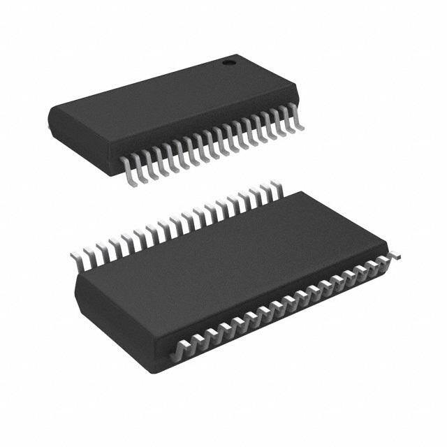
| 描述 | IC SCSI 27-LINE TERM 36-SSOPSCSI 接口集成电路 27line 3 5V SCSI SE |
| 产品分类 | |
| 品牌 | Texas Instruments |
| 产品手册 | |
| 产品图片 |
|
| rohs | 符合RoHS无铅 / 符合限制有害物质指令(RoHS)规范要求 |
| 产品系列 | 接口 IC,SCSI 接口集成电路,Texas Instruments UCC5620MWP- |
| 数据手册 | |
| 产品型号 | UCC5620MWP |
| PCN过时产品 | |
| 产品目录页面 | |
| 产品种类 | SCSI 接口集成电路 |
| 供应商器件封装 | 36-SSOP |
| 关闭 | Yes |
| 其它名称 | 296-6743-5 |
| 包装 | 管件 |
| 单位重量 | 723.400 mg |
| 商标 | Texas Instruments |
| 安装类型 | 表面贴装 |
| 安装风格 | SMD/SMT |
| 封装 | Tube |
| 封装/外壳 | 36-BSOP(0.295",7.50mm 宽) |
| 封装/箱体 | SSOP-36 |
| 工作温度 | 0°C ~ 70°C |
| 工作电源电压 | 4 V to 7 V |
| 工厂包装数量 | 25 |
| 最大工作温度 | + 70 C |
| 最小工作温度 | 0 C |
| 标准包装 | 25 |
| 激励器数量 | 1 |
| 电压-电源 | - |
| 电源电流 | 630 mA |
| 电阻 | 110 Ohms |
| 端子数 | 27 |
| 类型 | SCSI Termination |
| 系列 | UCC5620 |


- 商务部:美国ITC正式对集成电路等产品启动337调查
- 曝三星4nm工艺存在良率问题 高通将骁龙8 Gen1或转产台积电
- 太阳诱电将投资9.5亿元在常州建新厂生产MLCC 预计2023年完工
- 英特尔发布欧洲新工厂建设计划 深化IDM 2.0 战略
- 台积电先进制程称霸业界 有大客户加持明年业绩稳了
- 达到5530亿美元!SIA预计今年全球半导体销售额将创下新高
- 英特尔拟将自动驾驶子公司Mobileye上市 估值或超500亿美元
- 三星加码芯片和SET,合并消费电子和移动部门,撤换高东真等 CEO
- 三星电子宣布重大人事变动 还合并消费电子和移动部门
- 海关总署:前11个月进口集成电路产品价值2.52万亿元 增长14.8%


PDF Datasheet 数据手册内容提取
UCC5620 27-Line SCSI Terminator FEATURES DESCRIPTION • Complies with SCSI, SCSI-2, SCSI-3, UCC5620 provides 27 lines of active termination for a SCSI (Small Com- SPIand FAST-20 (Ultra) Standards puter Systems Interface) parallel bus. The SCSI standard recommends active termination at both ends of the cable. • 2.5pF Channel Capacitance during Disconnect The UCC5620 is ideal for high performance 5V SCSI systems. During disconnectthesupplycurrentistypicallyonly100µA,whichmakestheIC • 100mA Supply Current in Disconnect attractive for lower powered systems. Mode The UCC5620 is designed with a low channel capacitance of 2.5pF, • 4V To 7V Operation whicheliminateseffectsonsignalintegrityfromdisconnectedterminators • 110 Termination at interim points on the bus. • Completely Meets SCSI Hot Plugging The power amplifier output stage allows the UCC5620 to source full ter- mination current and sink active negation current when all termination • –900mA Sourcing Current for lines are actively negated. Termination TheUCC5620,aswithallUnitrodeterminators,iscompletelyhotplugga- • +500mA Sinking Current for Active ble and appears as high impedance at the teminating channels with Negation V = 0V or open. TRMPWR • Logic Command Disconnects all Internal circuit trimming is utilized, first to trim the 110 impedance, and Termination Lines thenmostimportantly,totrimtheoutputcurrentasclosetothemaximum • Trimmed Impedance to 5% SCSI-3 specification as possible, which maximizes noise margin in fast SCSI operation. • Current Limit and Thermal Shutdown Protection Other features include thermal shutdown and current limit.This device is offeredinlowthermalresistanceversionsoftheindustrystandard36-Pin Wide BodyQSOP(MWP). ConsultQSOP-36packaging diagram for exact dimensions. BLOCK DIAGRAM Circuit Design Patented UDG-96109 SLUS287B - OCTOBER 1999 - REVISED APRIL 2002
UCC5620 ABSOLUTE MAXIMUM RATINGS CONNECTION DIAGRAM TermpwrVoltage. . . . . . . . . . . . . . . . . . . . . . . . . . . . . . . . .+7V SSOP-36(Top View) Signal Line Voltage . . . . . . . . . . . . . . . . . . . . . . . . . .0V to +7V Regulator Output Current. . . . . . . . . . . . . . . . . . . . . . . . . .1.5A MWPPackage Storage Temperature. . . . . . . . . . . . . . . . . . .−65 C to +150 C Junction Temperature. . . . . . . . . . . . . . . . . . .−55 C to +150 C Lead Temperature (Soldering, 10 Sec.). . . . . . . . . . . . .+300 C LINE8 1 36 LINE7 Currentsarepositiveinto,negativeoutofthespecifiedtermi- LINE9 2 35 LINE6 nal.ConsultPackagingSectionofDatabookforthermallimita- tions and considerations of packages. LINE23 3 34 LINE5 LINE24 4 33 LINE22 LINE25 5 32 LINE21 LINE26 6 31 LINE20 LINE27 7 30 LINE19 GND 8 29 REG GND 9 28 GND GND 10 27 GND DISCNCT 11 26 GND LINE10 12 25 TRMPWR LINE11 13 24 LINE18 LINE12 14 23 LINE17 LINE13 15 22 LINE16 LINE14 16 21 LINE15 LINE1 17 20 LINE4 LINE2 18 19 LINE3 ELECTRICAL CHARACTERISTICSUnless otherwise stated, these specifications apply for T = 0°C to 70°C,TRMPWR A = 4.75V,DISCNCT= 0V, T =T . A J PARAMETER TEST CONDITIONS MIN TYP MAX UNITS Supply Current Section TRMPWRSupply Current All Termination Lines = Open 1 2 mA All Termination Lines = 0.2V 630 650 mA Power Down Mode DISCNCT=TRMPWR 100 200 µA Output Section (Termination Lines) Termination Impedance (Note 3) 104.5 110 115.5 Ω Output High Voltage (Note 1) 2.6 2.8 3.0 V Max Output Current V = 0.2V,T = 25°C −22.1 −23.3 −24 mA LINE J V = 0.2V −20.7 −23.3 −24 mA LINE V = 0.2V,TRMPWR= 4V,T = 25°C (Note 1) −21 −23 −24 mA LINE J V = 0.2V,TRMPWR= 4V (Note 1) −20 −23 −24 mA LINE V = 0.5V −22.4 mA LINE Output Leakage DISCNCT= 2.4V,TRMPWR= 0V to 5.25V 10 400 nA Output Capacitance DISCNCT= 2.4V (Note 2) 2.5 4 pF 2
UCC5620 ELECTRICAL CHARACTERISTICSUnless otherwise stated, these specifications apply for T = 0°C to 70°C,TRMPWR A = 4.75V,DISCNCT= 0V, T =T . A J PARAMETER TEST CONDITIONS MIN TYP MAX UNITS Regulator Section Regulator Output Voltage 2.6 2.8 3.0 V Drop Out Voltage All Termination Lines = 0.2V 0.4 0.8 V Short Circuit Current V = 0V −650 −900 –1300 mA REG Sinking Current Capability V = 3.5V 300 500 900 mA REG Thermal Shutdown 170 C° Thermal ShutdownHysteresis 10 C° Disconnect Section Disconnect Threshold 0.8 1.5 2.0 V Input Current DISCNCT= 0V –20 –60 µA Note 1:Measuring each termination line while other 26 are low (0.2V). Note 2:Ensured by design.Not 100% tested in production. (V N.L.−0.2V) Note 3:Tested by measuringI withV = 0.2V andV with no load, then calculate: Z= OUT OUT OUT OUT I at0.2V OUT PIN DESCRIPTIONS DISCNCT: Taking this pin high or leaving it open causes GND:Ground reference for the IC. all channels to become high impedance, and the chip to LINE1 - LINE27:110 termination channels. go into low-power mode;a low state allows the channels to provide normal termination. REG:Output of the internal 2.7V regulator. TRMPWR:Power for the IC. APPLICATION INFORMATION UCC5620 TRMPWR TRMPWR DISCNCT 4.7µF REG L1 L27 4.7µF DATABYTES1AND2 CONTROLBITS +2PARITYBITS TODRIVERS ANDRECEIVERS TOSCSIBUS UDG-98188 Figure 1.Typical Wide SCSI Bus Configuration Using the UCC5620 3
PACKAGE OPTION ADDENDUM www.ti.com 18-Feb-2005 PACKAGING INFORMATION OrderableDevice Status(1) Package Package Pins Package EcoPlan(2) Lead/BallFinish MSLPeakTemp(3) Type Drawing Qty UCC5620FQPTR OBSOLETE LQFP PT 48 None CallTI CallTI UCC5620MWP ACTIVE SSOP DCE 36 25 None CUSNPB Level-1-220C-UNLIM UCC5620MWPTR ACTIVE SSOP DCE 36 1000 None CUSNPB Level-1-220C-UNLIM (1)Themarketingstatusvaluesaredefinedasfollows: ACTIVE:Productdevicerecommendedfornewdesigns. LIFEBUY:TIhasannouncedthatthedevicewillbediscontinued,andalifetime-buyperiodisineffect. NRND:Notrecommendedfornewdesigns.Deviceisinproductiontosupportexistingcustomers,butTIdoesnotrecommendusingthispartin anewdesign. PREVIEW:Devicehasbeenannouncedbutisnotinproduction.Samplesmayormaynotbeavailable. OBSOLETE:TIhasdiscontinuedtheproductionofthedevice. (2)EcoPlan-Maynotbecurrentlyavailable-pleasecheckhttp://www.ti.com/productcontentforthelatestavailabilityinformationandadditional productcontentdetails. None:NotyetavailableLead(Pb-Free). Pb-Free(RoHS):TI'sterms"Lead-Free"or"Pb-Free"meansemiconductorproductsthatarecompatiblewiththecurrentRoHSrequirements forall6substances,includingtherequirementthatleadnotexceed0.1%byweightinhomogeneousmaterials.Wheredesignedtobesoldered athightemperatures,TIPb-Freeproductsaresuitableforuseinspecifiedlead-freeprocesses. Green (RoHS & no Sb/Br): TI defines "Green" to mean "Pb-Free" and in addition, uses package materials that do not contain halogens, includingbromine(Br)orantimony(Sb)above0.1%oftotalproductweight. (3) MSL, Peak Temp. -- The Moisture Sensitivity Level rating according to the JEDECindustry standard classifications, and peak solder temperature. Important Information and Disclaimer:The information provided on this page represents TI's knowledge and belief as of the date that it is provided. TI bases its knowledge and belief on information provided by third parties, and makes no representation or warranty as to the accuracy of such information. Efforts are underway to better integrate information from third parties. TI has taken and continues to take reasonable steps to provide representative and accurate information but may not have conducted destructive testing or chemical analysis on incomingmaterialsandchemicals.TIandTIsuppliersconsidercertaininformationtobeproprietary,andthusCASnumbersandotherlimited informationmaynotbeavailableforrelease. InnoeventshallTI'sliabilityarisingoutofsuchinformationexceedthetotalpurchasepriceoftheTIpart(s)atissueinthisdocumentsoldbyTI toCustomeronanannualbasis. Addendum-Page1
IMPORTANT NOTICE Texas Instruments Incorporated and its subsidiaries (TI) reserve the right to make corrections, modifications, enhancements, improvements, and other changes to its products and services at any time and to discontinue any product or service without notice. Customers should obtain the latest relevant information before placing orders and should verify that such information is current and complete. All products are sold subject to TI’s terms and conditions of sale supplied at the time of order acknowledgment. TI warrants performance of its hardware products to the specifications applicable at the time of sale in accordance with TI’s standard warranty. Testing and other quality control techniques are used to the extent TI deems necessary to support this warranty. Except where mandated by government requirements, testing of all parameters of each product is not necessarily performed. TI assumes no liability for applications assistance or customer product design. Customers are responsible for their products and applications using TI components. To minimize the risks associated with customer products and applications, customers should provide adequate design and operating safeguards. TI does not warrant or represent that any license, either express or implied, is granted under any TI patent right, copyright, mask work right, or other TI intellectual property right relating to any combination, machine, or process in which TI products or services are used. Information published by TI regarding third-party products or services does not constitute a license from TI to use such products or services or a warranty or endorsement thereof. Use of such information may require a license from a third party under the patents or other intellectual property of the third party, or a license from TI under the patents or other intellectual property of TI. Reproduction of information in TI data books or data sheets is permissible only if reproduction is without alteration and is accompanied by all associated warranties, conditions, limitations, and notices. Reproduction of this information with alteration is an unfair and deceptive business practice. TI is not responsible or liable for such altered documentation. Resale of TI products or services with statements different from or beyond the parameters stated by TI for that product or service voids all express and any implied warranties for the associated TI product or service and is an unfair and deceptive business practice. TI is not responsible or liable for any such statements. Following are URLs where you can obtain information on other Texas Instruments products and application solutions: Products Applications Amplifiers amplifier.ti.com Audio www.ti.com/audio Data Converters dataconverter.ti.com Automotive www.ti.com/automotive DSP dsp.ti.com Broadband www.ti.com/broadband Interface interface.ti.com Digital Control www.ti.com/digitalcontrol Logic logic.ti.com Military www.ti.com/military Power Mgmt power.ti.com Optical Networking www.ti.com/opticalnetwork Microcontrollers microcontroller.ti.com Security www.ti.com/security Telephony www.ti.com/telephony Video & Imaging www.ti.com/video Wireless www.ti.com/wireless Mailing Address: Texas Instruments Post Office Box 655303 Dallas, Texas 75265 Copyright 2005, Texas Instruments Incorporated