ICGOO在线商城 > 集成电路(IC) > PMIC - AC-DC 转换器,离线开关 > UCC3895DWTR
 Datasheet下载
- 型号: UCC3895DWTR
- 制造商: Texas Instruments
- 库位|库存: xxxx|xxxx
- 要求:
| 数量阶梯 | 香港交货 | 国内含税 |
| +xxxx | $xxxx | ¥xxxx |
查看当月历史价格
查看今年历史价格
UCC3895DWTR产品简介:
ICGOO电子元器件商城为您提供UCC3895DWTR由Texas Instruments设计生产,在icgoo商城现货销售,并且可以通过原厂、代理商等渠道进行代购。 UCC3895DWTR价格参考¥11.44-¥14.29。Texas InstrumentsUCC3895DWTR封装/规格:PMIC - AC-DC 转换器,离线开关, Converter Offline Full-Bridge Topology 1MHz 20-SOIC。您可以下载UCC3895DWTR参考资料、Datasheet数据手册功能说明书,资料中有UCC3895DWTR 详细功能的应用电路图电压和使用方法及教程。
| 参数 | 数值 |
| 产品目录 | 集成电路 (IC)半导体 |
| Cuk | 无 |
| 描述 | IC REG CTRLR PWM CM/VM 20-SOIC开关控制器 BiCMOS Advanced Phase Shift |
| DevelopmentKit | UCC3895EVM-001 |
| 产品分类 | |
| 品牌 | Texas Instruments |
| 产品手册 | |
| 产品图片 |
|
| rohs | 符合RoHS无铅 / 符合限制有害物质指令(RoHS)规范要求 |
| 产品系列 | 电源管理 IC,开关控制器 ,Texas Instruments UCC3895DWTR- |
| 数据手册 | |
| 产品型号 | UCC3895DWTR |
| PWM类型 | 电流/电压模式 |
| 产品种类 | 开关控制器 |
| 倍增器 | 无 |
| 其它名称 | 296-27167-6 |
| 分频器 | 无 |
| 包装 | Digi-Reel® |
| 升压 | 是 |
| 单位重量 | 569 mg |
| 占空比 | 100% |
| 反向 | 无 |
| 反激式 | 无 |
| 商标 | Texas Instruments |
| 安装风格 | SMD/SMT |
| 封装 | Reel |
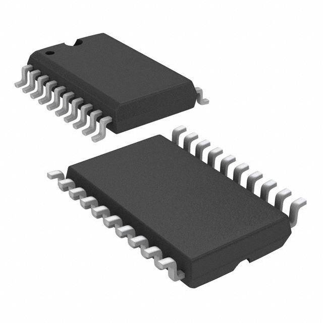
| 封装/外壳 | 24-SOIC(0.295",7.50mm 宽) |
| 封装/箱体 | SOIC-20 |
| 工作温度 | 0°C ~ 70°C |
| 工作电源电压 | 9 V to 16.5 V |
| 工厂包装数量 | 2000 |
| 开关频率 | 1000 kHz |
| 拓扑结构 | Buck, Boost, Full-Bridge |
| 最大工作温度 | + 70 C |
| 最小工作温度 | 0 C |
| 标准包装 | 1 |
| 电压-电源 | 10 V ~ 16.5 V |
| 类型 | BiCMOS Advanced Phase Shift Resonant Controller |
| 系列 | UCC3895 |
| 输出数 | 4 |
| 输出电流 | 100 mA |
| 输出端数量 | 4 Output |
| 配用 | /product-detail/zh/UCC3895EVM-001/296-20628-ND/562087 |
| 降压 | 是 |
| 隔离式 | 是 |
| 频率-最大值 | 1MHz |


- 商务部:美国ITC正式对集成电路等产品启动337调查
- 曝三星4nm工艺存在良率问题 高通将骁龙8 Gen1或转产台积电
- 太阳诱电将投资9.5亿元在常州建新厂生产MLCC 预计2023年完工
- 英特尔发布欧洲新工厂建设计划 深化IDM 2.0 战略
- 台积电先进制程称霸业界 有大客户加持明年业绩稳了
- 达到5530亿美元!SIA预计今年全球半导体销售额将创下新高
- 英特尔拟将自动驾驶子公司Mobileye上市 估值或超500亿美元
- 三星加码芯片和SET,合并消费电子和移动部门,撤换高东真等 CEO
- 三星电子宣布重大人事变动 还合并消费电子和移动部门
- 海关总署:前11个月进口集成电路产品价值2.52万亿元 增长14.8%


PDF Datasheet 数据手册内容提取
UCC1895, UCC2895, UCC3895 www.ti.com SLUS157P –DECEMBER1999–REVISEDJUNE2013 BiCMOS Advanced Phase-Shift PWM Controller CheckforSamples:UCC1895,UCC2895,UCC3895 FEATURES DESCRIPTION 1 • Programmable-OutputTurnonDelay The UCC3895 is a phase-shift PWM controller that implements control of a full-bridge power stage by • AdaptiveDelaySet phase shifting the switching of one half-bridge with • BidirectionalOscillatorSynchronization respect to the other. The device allows constant • Voltage-Mode,PeakCurrent-Mode,orAverage frequency pulse-width modulation in conjunction with Current-ModeControl resonant zero-voltage switching to provide high efficiency at high frequencies. The part is used either • ProgrammableSoftstart,SoftstopandChip asavoltage-modeorcurrent-modecontroller. DisableviaaSinglePin While the UCC3895 maintains the functionality of the • 0%to100%Duty-CycleControl UC3875/6/7/8 family and UC3879, it improves on that • 7-MHzErrorAmplifier controller family with additional features such as • Operationto1MHz enhanced control logic, adaptive delay set, and shutdowncapability.Becausethedeviceisbuiltusing • Typical5-mAOperatingCurrentat500kHz the BCDMOS process, it operates with dramatically • VeryLow150-μACurrentDuringUVLO less supply current than it’s bipolar counterparts. The UCC3895 operates with a maximum clock frequency APPLICATIONS of1MHz. • Phase-ShiftedFull-BridgeConverters • Off-Line,Telecom,DatacomandServers • DistributedPowerArchitecture • High-DensityPowerModules UCC3895 Q1 1 EAN EAP 27777777770 VOUT 2 EAOUT SS/DISB 19 3 RAMP OUTA 18 4 REF OUTB 17 A C 5 GND PGND 16 VIN 6 SYNC VCC 15 VBIAS 7 CT OUTC 14 B D 8 RT OUTD 13 9 DELAB CS 12 10 DELCD ADS 11 1 Pleasebeawarethatanimportantnoticeconcerningavailability,standardwarranty,anduseincriticalapplicationsof TexasInstrumentssemiconductorproductsanddisclaimerstheretoappearsattheendofthisdatasheet. PRODUCTIONDATAinformationiscurrentasofpublicationdate. Copyright©1999–2013,TexasInstrumentsIncorporated Products conform to specifications per the terms of the Texas Instruments standard warranty. Production processing does not necessarilyincludetestingofallparameters.
UCC1895, UCC2895, UCC3895 SLUS157P –DECEMBER1999–REVISEDJUNE2013 www.ti.com This integrated circuit can be damaged by ESD. Texas Instruments recommends that all integrated circuits be handled with appropriateprecautions.Failuretoobserveproperhandlingandinstallationprocedurescancausedamage. ESDdamagecanrangefromsubtleperformancedegradationtocompletedevicefailure.Precisionintegratedcircuitsmaybemore susceptibletodamagebecauseverysmallparametricchangescouldcausethedevicenottomeetitspublishedspecifications. ORDERINGINFORMATION PACKAGEDDEVICES T A SOIC-20(DW)(1) PDIP-20(N) TSSOP-20(PW)(1) PLCC-20(FN)(1) LCCC-20(FK) CDIP-20(J) –55°Cto+125°C UCC1895L UCC1895J –40°Cto+85°C UCC2895DW UCC2895N UCC2895PW UCC2895Q 0°Cto70°C UCC3895DW UCC3895N UCC3895PW UCC3895Q (1) TheDW,PWandQpackagesareavailabletapedandreeled.AddTRsuffixtodevicetype(forexample:UCC2895DWTR)toorder quantitiesof2000devicesperreelforDW. ABSOLUTE MAXIMUM RATINGS Allvoltagevaluesarewithrespecttothenetworkgroundterminalunlessotherwisenoted.(1) VALUE UNIT MIN MAX Supplyvoltage 17 V Outputcurrent 100 Referencecurrent 15 mA Supplycurrent 30 Analoginputs EAP,EAN,EAOUT,RAMP,SYNC,ADS,CS, –0.3 REF+0.3 V SS/DISB Driveoutputs OUTA,OUTB,OUTC,OUTD –0.3 VCC+0.3 PowerdissipationatT =25°C DW-20package 650 mW A N-20package 1 W T Junctiontemperaturerange –55 150 J Leadtemperature1.6mm(1/16in)fromcasefor10seconds 300 °C T Storagetemperaturerange –65 150 stg (1) Stressesbeyondthoselistedunderabsolutemaximumratingsmaycausepermanentdamagetothedevice.Thesearestressratings only,andfunctionaloperationofthedeviceattheseoranyotherconditionsbeyondthoseindicatedunderrecommendedoperating conditionsisnotimplied.ExposuretoAbsoluteMaximumRatedconditionsforextendedperiodsmayaffectdevicereliability THERMAL CHARACTERISTICS PART T T UNIT JA JC UCC2895DW 90 25 UCC2895N 80 35 UCC2895PW 125 14 °C/W UCC2895Q 75 34 UCC1895J 85 28 UCC1895L 80 20 2 SubmitDocumentationFeedback Copyright©1999–2013,TexasInstrumentsIncorporated ProductFolderLinks:UCC1895 UCC2895 UCC3895
UCC1895, UCC2895, UCC3895 www.ti.com SLUS157P –DECEMBER1999–REVISEDJUNE2013 RECOMMENDED OPERATING CONDITIONS(1) MIN NOM MAX UNIT V Supplyvoltage 10 16.5 V DD V Supplyvoltagebypasscapacitor(2) 10×C DD REF C Referencebypasscapacitor(UCC1895)(3) 0.1 1.0 µF REF C Referencebypasscapacitor(UCC2895,UCC3895)(3) 0.1 4.7 REF C Timingcapacitor(for500-kHzswitchingfrequency) 220 pF T R Timingresistor(for500-kHzswitchingfrequency) 82 T kΩ R ,R Delayresistor 2.5 40 DEL_AB DEL_CD T Operatingjunctiontemperature(4) –55 125 °C J (1) TIrecommendsthattherebeasinglepointgroundedbetweenGNDandPGNDdirectlyunderthedevice.Theremustbeaseparate groundplaneassociatedwiththeGNDpinandallcomponentsassociatedwithpins1through12,plus19and20,belocatedoverthis groundplane.Anyconnectionsassociatedwiththesepinstogroundmustbeconnectedtothisgroundplane. (2) TheV capacitormustbealowESR,ESLceramiccapacitorlocateddirectlyacrosstheVDDandPGNDpins.Alargerbulkcapacitor DD mustbelocatedasphysicallycloseaspossibletotheV pins. DD (3) TheV capacitormustbealowESR,ESLceramiccapacitorlocateddirectlyacrosstheREFandGNDpins.Ifalargercapacitoris REF desiredfortheV thenitmustbelocatedneartheV capandconnectedtotheV pinwitharesistorof51Ωorgreater.Thebulk REF REF REF capacitoronV mustbeafactorof10greaterthanthetotalV capacitance. DD REF (4) TIdoesnotrecommendedthatthedeviceoperateunderconditionsbeyondthosespecifiedinthistableforextendedperiodsoftime. ELECTRICAL CHARACTERISTICS V =12V,R =82kΩ,C =220pF,R =10kΩ,R =10kΩ,C =0.1μF,C =0.1μFandnoloadonthe DD T T DELAB DELCD REF VDD outputs,T =T.T =0°Cto70°CforUCC3895x,T =–40°Cto+85°CforUCC2895xandT =–55°Cto+125°Cforthe A J A A A UCC1895x.(unlessotherwisenoted) PARAMETER TESTCONDITIONS MIN TYP MAX UNIT UVLO(UNDERVOLTAGELOCKOUT) UVLO Start-upvoltagethreshold 10.2 11 11.8 (on) UVLO Minimumoperatingvoltageafter 8.2 9 9.8 (off) V start-up UVLO Hysteresis 1 2 3 (hys) SUPPLY I Start-upcurrent VDD=8V 150 250 µA START I Operatingcurrent 5 6 mA DD V V clampvoltage IDD=10mA 16.5 17.5 18.5 V DD_CLAMP DD VOLTAGEREFERENCE V Outputvoltage T =25°C 4.94 5 5.06 REF J 10V<VDD<VDD_CLAMP 4.85 5 5.15 V 0mA<IREF<5mA temperature I Shortcircuitcurrent REF=0V,T =25°C 10 20 mA SC J ERRORAMPLIFIER Common-modeinputvoltagerange –0.1 3.6 V V Offsetvoltage –7 7 mV IO I Inputbiascurrent(EAP,EAN) –1 1 µA BIAS EAOUT High-leveloutputvoltage EAP-EAN=500mV,I =–0.5mA 4 4.5 5 _VOH EAOUT V EAOUT Low-leveloutputvoltage EAP-EAN=–500mV,I =0.5mA 0 0.2 0.4 _VOL EAOUT I Erroramplifieroutputsourcecurrent EAP-EAN=500mV,EAOUT=2.5V 1 1.5 SOURCE mA I Erroramplifieroutputsinkcurrent EAP-EAN=–500mV,EAOUT=2.5V 2.5 4.5 SINK A Open-loopdcgain 75 85 dB VOL GBW Unitygainbandwidth(1) 5 7 mHz Slewrate(1) 1V<EAN<0V,EAP=500mV 1.5 2.2 V/µs 0.5V<EAOUT<3V (1) Ensuredbydesign.Notproductiontested. Copyright©1999–2013,TexasInstrumentsIncorporated SubmitDocumentationFeedback 3 ProductFolderLinks:UCC1895 UCC2895 UCC3895
UCC1895, UCC2895, UCC3895 SLUS157P –DECEMBER1999–REVISEDJUNE2013 www.ti.com ELECTRICAL CHARACTERISTICS (continued) V =12V,R =82kΩ,C =220pF,R =10kΩ,R =10kΩ,C =0.1μF,C =0.1μFandnoloadonthe DD T T DELAB DELCD REF VDD outputs,T =T.T =0°Cto70°CforUCC3895x,T =–40°Cto+85°CforUCC2895xandT =–55°Cto+125°Cforthe A J A A A UCC1895x.(unlessotherwisenoted) PARAMETER TESTCONDITIONS MIN TYP MAX UNIT No-loadcomparatorturn-offthreshold 0.45 0.5 0.55 No-loadcomparatorturn-onthreshold 0.55 0.6 0.69 V No-loadcomparatorhysteresis 0.035 0.1 0.165 OSCILLATOR f Frequency T =25°C 473 500 527 kHZ OSC J Frequencytotalvariation( Overline,temperature 2.5% 5% V SYNCinputthreshold,SYNC 2.05 2.1 2.4 IH_SYNC V High-leveloutputvoltage,SYNC I =–400μA,V =2.6V 4.1 4.5 5 V OH_SYNC SYNC CT V Low-leveloutputvoltage,SYNC I =100μA,V =0V 0 0.5 1 OL_SYNC SYNC CT Syncoutputpulsewidth LOAD =3.9kΩand30pFinparallel 85 135 ns SYNC V Timingresistorvoltage 2.9 3 3.1 RT V Timingcapacitorpeakvoltage 2.25 2.35 2.55 v CT(peak) V Timingcapacitorvalleyvoltage 0 0.2 0.4 CT(valley) CURRENTSENSE I Currentsensebiascurrent 0V<CS<2.5V –4.5 20 µA CS(bias) 0VADS<2.5V Peakcurrentthreshold 1.9 2 2.1 V Overcurrentthreshold 2.4 2.5 2.6 V Currentsensetooutputdelay 0V≤CS≤2.3V 75 110 ns DELAB=DELCD=REF SOFT-START/SHUTDOWN I Softstartsourcecurrent SS/DISB=3.0V –40 –35 –30 µA SOURCE CS=1.9V I Softstartsinkcurrent SS/DISB=3.0V, 325 350 375 µA SINK CS=2.6V Softstart/disablecomparator 0.44 0.5 0.56 V threshold ADAPTIVEDELAYSET(ADS) DELAB/DELCDoutputvoltage ADS=CS=0V 0.45 0.5 0.55 ADS=0V 1.9 2 2.1 V CS=2V t Outputdelay(2)(3) ADS=CS=0V 450 560 620 ns DELAY ADSbiascurrent 0V<ADS<2.5V –20 20 µA 0V<CS<2.5V (2) Ensuredbydesign.Notproductiontested. (3) OutputdelayismeasuredbetweenOUTAandOUTB,orOUTCandOUTD.Outputdelayisdefinedasshownbelowwhere:t = f(OUTA) fallingedgeofOUTAsignal,t =risingedgeofOUTBsignal(seeFigure1andFigure2). r(OUTB) 4 SubmitDocumentationFeedback Copyright©1999–2013,TexasInstrumentsIncorporated ProductFolderLinks:UCC1895 UCC2895 UCC3895
UCC1895, UCC2895, UCC3895 www.ti.com SLUS157P –DECEMBER1999–REVISEDJUNE2013 ELECTRICAL CHARACTERISTICS (continued) V =12V,R =82kΩ,C =220pF,R =10kΩ,R =10kΩ,C =0.1μF,C =0.1μFandnoloadonthe DD T T DELAB DELCD REF VDD outputs,T =T.T =0°Cto70°CforUCC3895x,T =–40°Cto+85°CforUCC2895xandT =–55°Cto+125°Cforthe A J A A A UCC1895x.(unlessotherwisenoted) PARAMETER TESTCONDITIONS MIN TYP MAX UNIT OUTPUT V High--leveloutputvoltage(all I =–10mA,VDDtooutput 250 400 mV OH OUT outputs) V Low-leveloutputvoltage(alloutputs) I =10mA 150 250 mV OL OUT t Risetime(4) C =100pF 20 35 ns R LOAD t Falltime(4) C =100pF 20 35 ns F LOAD PWMCOMPARATOR EAOUTtoRAMPinputoffsetvoltage RAMP=0V 0.72 0.85 1.05 V DELAB=DELCD=REF Minimumphaseshift(5) RAMP=0V 0.0% 0.85% 1.4% (OUTAtoOUTC,OUTBtoOUTD) EAOUT=650mV t Delay(6) 0V<RAMP<2.5V,EAOUT=1.2V 70 120 ns DELAY (RAMPtoOUTC,RAMPtoOUTD) DELAB=DELCD=REF I RAMPbiascurrent RAMP<5V,CT=2.2V –5 5 µA R(bias) I RAMPsinkcurrent RAMP=5V,CT=2.6V 12 19 mA R(sink) (4) Ensuredbydesign.Notproductiontested. (5) Minimumphaseshiftisdefinedas: t -t t -t f(OUTC) f(OUTA) f(OUTC) f(OUTB) F =180´ or F =180´ t t PERIOD PERIOD where (a)t =fallingedgeofOUTAsignal f(OUTA) (b)t =fallingedgeofOUTBsignal f(OUTB) (c)t =fallingedgeofOUTCsignal, f(OUTC) (d)t =fallingedgeofOUTDsignal f(OUTD) (e)t =periodofOUTAorOUTBsignal PERIOD (6) OutputdelayismeasuredbetweenOUTAandOUTB,orOUTCandOUTD.Outputdelayisdefinedasshownbelowwhere:t = f(OUTA) fallingedgeofOUTAsignal,t =risingedgeofOUTBsignal(seeFigure1andFigure2). r(OUTB) tPERIOD OUTA OUTA tDELAY = tR(OUTB) - tf(OUTA) tDELAY = tf(OUTA) - tf(OUTC) OUTB OUTC Figure2. SameAppliestoOUTCandOUTD Figure1. SameAppliestoOUTBandOUTD Copyright©1999–2013,TexasInstrumentsIncorporated SubmitDocumentationFeedback 5 ProductFolderLinks:UCC1895 UCC2895 UCC3895
UCC1895, UCC2895, UCC3895 SLUS157P –DECEMBER1999–REVISEDJUNE2013 www.ti.com DEVICE INFORMATION PWANDDWPACKAGEDRAWINGS NANDJPACKAGEDRAWINGS (TOPVIEW) (TOPVIEW) PWandDWPACKAGE (TOPVIEW) EAN 1 20 EAP EAOUT 2 19 SS/DISB EAN 1 20 EAP EAOUT 2 19 SS/DISB RAMP 3 18 OUTA RAMP 3 18 OUTA REF 4 17 OUTB REF 4 17 OUTB GND 5 16 PGND GND 5 16 PGND SYNC 6 15 VDD SYNC 6 15 VDD CT 7 14 OUTC CT 7 14 OUTC RT 8 13 OUTD RT 8 13 OUTD DELAB 9 12 CS DELAB 9 12 CS DELCD 10 11 ADS DELCD 10 11 ADS FNANDFKPACKAGEDRAWINGS (TOPVIEW) EAN EAOUT EAP RAMP SS/DISB 3 2 1 20 19 REF 4 18 OUTA GND 5 17 OUTB SYNC 6 16 PGND CT 7 15 VDD RT 8 14 OUTC 9 10 11 12 13 DELAB OUTD DELCD CS ADS TERMINALFUNCTIONS TERMINAL I/O DESCRIPTION NAME NO. Theadaptive-delay-setpinsetstheratiobetweenthemaximumandminimumprogrammedoutputdelay ADS 11 I deadtime. CS 12 I Currentsenseinputforcycle-by-cyclecurrentlimitingandforover-currentcomparator. Oscillatortimingcapacitorforprogrammingtheswitchingfrequency.TheUCC3895oscillatorchargesCTvia CT 7 I aprogrammedcurrent. Thedelay-programmingbetweencomplementary-outputspin,DELAB,programsthedeadtimebetween DELAB 9 I switchingofoutputAandoutputB. Thedelay-programmingbetweencomplementary-outputspin,DELCD,programsthedeadtimebetween DELCD 10 I switchingofoutputCandoutputD. EAOUT 2 I/O Erroramplifieroutput. EAP 20 I Non-invertinginputtotheerroramplifier.Keepbelow3.6Vforproperoperation. EAN 1 I Invertinginputtotheerroramplifier.Keepbelow3.6Vforproperoperation. GND 5 - Chipgroundforallcircuitsexcepttheoutputstages. 6 SubmitDocumentationFeedback Copyright©1999–2013,TexasInstrumentsIncorporated ProductFolderLinks:UCC1895 UCC2895 UCC3895
UCC1895, UCC2895, UCC3895 www.ti.com SLUS157P –DECEMBER1999–REVISEDJUNE2013 TERMINALFUNCTIONS(continued) TERMINAL I/O DESCRIPTION NAME NO. OUTA 18 O OUTB 17 O Thefouroutputsare100-mAcomplementaryMOSdrivers,andareoptimizedtodriveFETdrivercircuits OUTC 14 O suchasUCC27424orgatedrivetransformers. OUTD 13 O PGND 16 - Outputstageground. RAMP 3 I InvertinginputofthePWMcomparator. 5V,±1.2%,5mAvoltagereference.Forbestperformance,bypasswitha0.1-μFlowESR,lowESL REF 4 O capacitortoground.Donotusemorethan4.7μFoftotalcapacitanceonthispin. RT 8 I Oscillatortimingresistorforprogrammingtheswitchingfrequency. SS/DISB 19 I Soft-startanddisablepinwhichcombinesthetwoindependentfunctions. SYNC 6 I/O Theoscillatorsynchronizationpinisbidirectional. Thepowersupplyinputpin,VDD,mustbebypassedwithaminimumofa1-μFlowESR,lowESLcapacitor VDD 15 I toground.Theadditionofa10-μFlowESR,lowESLbetweenVDDandPGNDisrecommended. Copyright©1999–2013,TexasInstrumentsIncorporated SubmitDocumentationFeedback 7 ProductFolderLinks:UCC1895 UCC2895 UCC3895
UCC1895, UCC2895, UCC3895 SLUS157P –DECEMBER1999–REVISEDJUNE2013 www.ti.com BLOCK DIAGRAM IRT RT 8 Q 15 VDD D S Q 8(IRT) OSC CT 7 Q OUTA D SQ DELAY A 18 Q R 9 DELAB SYNC 6 PWM R Q DELAY B 17 OUTB COMPARATOR RAMP 3 + 0.8 V + EAOUT 2 14 OUTC ERROR D S Q DELAY C EAP 20 AMP CONMOP ALROAATDO R 10 DELCD + + R Q DELAY D EAN 1 13 OUTD CURRENT SENSE COMPARATOR 0.5 V / 0.6 V 2 V + 16 PGND CS 12 11 ADS OVER CURRENT ADAPTIVE DELAY COMPARATOR + SET AMPLIFIER 2.5 V + 0.5V Q S UVLO COMPARATOR + REF Q R 11 V / 9 V DISABLE IRT COMPARATOR REF 4 REF HI=ON 0.5 V REFERENCE OK SS 19 + COMPARATOR HI=ON 4 V 5 GND + 10(IRT) REF VREF RT 8IRT RT IRT CT 2.5 V S Q CLOCK + CT 0.2 V + R SYNC CLOCK Figure3. OscillatorBlockDiagram 8 SubmitDocumentationFeedback Copyright©1999–2013,TexasInstrumentsIncorporated ProductFolderLinks:UCC1895 UCC2895 UCC3895
UCC1895, UCC2895, UCC3895 www.ti.com SLUS157P –DECEMBER1999–REVISEDJUNE2013 REF 0.5 V TO DELAY A 100 k: 75 k: + AND DELAY B BLOCKS CS DELAB + 100 k: ADS 75 k: REF TO DELAY C + AND DELAY D DELCD BLOCKS Figure4. AdaptiveDelaySetBlockDiagram REF BUSSED CURRENT FROM ADS CIRCUIT 3.5 V DELAB/CD FROM PAD DELAYED 2.5 V CLOCK SIGNAL CLOCK Figure5. DelayBlockDiagram(OneDelayBlockPerOutlet) Copyright©1999–2013,TexasInstrumentsIncorporated SubmitDocumentationFeedback 9 ProductFolderLinks:UCC1895 UCC2895 UCC3895
UCC1895, UCC2895, UCC3895 SLUS157P –DECEMBER1999–REVISEDJUNE2013 www.ti.com DETAILED PIN DESCRIPTION ADS (Adaptive Delay Set) This function sets the ratio between the maximum and minimum programmed output-delay dead time. When the ADS pin is directly connected to the CS pin, no delay modulation occurs. The maximum delay modulation occurs whenADSisgrounded.Inthiscase,delaytimeisfour-timeslongerwhenCS=0thanwhenCS=2V(thepeak- currentthreshold),ADSchangestheoutputvoltageonthedelaypinsDELABandDELCDbyEquation1. V = é0.75´(V -V )ù+0.5 V DEL ë CS ADS û where • V andV areinvolts (1) CS ADS ADS must be limited to between 0 V and 2.5 V and must be less-than or equal-to CS. DELAB and DELCD are clampedtoaminimumof0.5V. CS (Current Sense) The CS input connects to the inverting input of the current-sense comparator and the non-inverting input of the overcurrent comparator and the ADS amplifier. The current sense signal is used for cycle-by-cycle current limiting in peak current-mode control, and for overcurrent protection in all cases with a secondary threshold for outputshutdown.Anoutputdisableinitiatedbyanovercurrentfaultalsoresultsinarestartcycle,calledsoft-stop, withfullsoft-start. CT (Oscillator Timing Capacitor) The UCC3895 oscillator charges CT via a programmed current. The waveform on C is a sawtooth, with a peak T voltageof2.35V.TheapproximateoscillatorperiodiscalculatedbyEquation2. 5´R ´C t = T T +120ns OSC 48 where • C isinFarads T • R isinOhms T • t isinseconds OSC • C canrangefrom100to880pF. (2) T NOTE A large C and a small R combination results in extended fall times on the C waveform. T T T The increased fall time increases the SYNC pulse width, hence limiting the maximum phase shift between OUTA, OUTB and OUTC, OUTD outputs, which limits the maximum dutycycleoftheconverter(seetoFigure3). DELAB and DELCD (Delay Programming Between Complementary Outputs) DELAB programs the dead time between switching of OUTA and OUTB. DELCD programs the dead time between OUTC and OUTD. This delay is introduced between complementary outputs in the same leg of the external bridge. The UCC2895N allows the user to select the delay, in which the resonant switching of the external power stages takes place. Separate delays are provided for the two half-bridges to accommodate differencesinresonant-capacitorchargingcurrents.ThedelayineachstageissetaccordingtoEquation3. (25´10-12)´R DEL t = +25ns DELAY V DEL where • V isinvolts DEL • R isinOhms DEL • t isinseconds (3) DELAY 10 SubmitDocumentationFeedback Copyright©1999–2013,TexasInstrumentsIncorporated ProductFolderLinks:UCC1895 UCC2895 UCC3895
UCC1895, UCC2895, UCC3895 www.ti.com SLUS157P –DECEMBER1999–REVISEDJUNE2013 DELAB and DELCD source about 1 mA maximum. Choose the delay resistors so that this maximum is not exceeded. Programmable output delay is defeated by tying DELAB and, or, DELCD to REF. For an optimum performancekeepstraycapacitanceonthesepinsatlessthan10pF. EAOUT, EAP, and EAN (Error Amplifier) EAOUT connects internally to the non-inverting input of the PWM comparator and the no-load comparator. EAOUT is internally clamped to the soft-start voltage. The no-load comparator shuts down the output stages whenEAOUTfallsbelow500mV,andallowstheoutputstoturnonagainwhenEAOUTrisesabove600mV. EAPisthenon-invertingandtheEANistheinvertinginputtotheerroramplifier. OUTA, OUTB, OUTC, and OUTD (Output MOSFET Drivers) The four outputs are 100-mA complementary MOS drivers, and are optimized to drive MOSFET driver circuits. OUTA and OUTB are fully complementary, (assuming no programming delay) and operate near 50% duty cycle andone-halftheoscillatorfrequency.OUTAandOUTBareintendedtodriveonehalf-bridgecircuitinanexternal power stage. OUTC and OUTD drive the other half-bridge and have the same characteristics as OUTA and OUTB.OUTCisphaseshiftedwithrespecttoOUTA,andOUTDisphaseshiftedwithrespecttoOUTB. NOTE Changing the phase relationship of OUTC and OUTD with respect to OUTA and OUTB requires other than the nominal 50% duty ratio on OUTC and OUTD during those transients. PGND (Power Ground) To keep output switching noise from critical analog circuits, the UCC3895 has two different ground connections. PGNDisthegroundconnectionforthehigh-currentoutputstages.BothGNDandPGNDmustbeelectricallytied together.Also,becausePGNDcarrieshighcurrent,boardtracesmustbelowimpedance. RAMP (Inverting Input of the PWM Comparator) This pin receives either the C waveform in voltage and average current-mode controls, or the current signal T (plusslopecompensation)inpeakcurrent-modecontrol. REF (Voltage Reference) The 5-V ± 1.2% reference supplies power to internal circuitry, and also supplies up to 5 mA to external loads. The reference is shutdown during undervoltage lockout but is operational during all other disable modes. For best performance, bypass with a 0.1-μF low-ESR low-ESL capacitor to GND. To ensure the stability of the internalreference,donotusemorethan1.0μFoftotalcapacitanceonthispinfortheUCC1895. For the UCC2895 and the UCC3895, this capacitance increases as per the limits defined in the RECOMMENDEDOPERATINGCONDITIONStableofthisspecification. RT (Oscillator Timing Resistor) The oscillator in the UCC3895 operates by charging an external timing capacitor, C , with a fixed current T programmedbyR .R currentiscalculatedwithEquation4. T T 3 V I (A)= RT R (W) T (4) R ranges from 40 to 120 kΩ. Soft-start charging and discharging currents are also programmed by I (Refer to T RT Figure3). GND (Analog Ground) Thispinisthechipgroundforallinternalcircuitsexcepttheoutputstages. Copyright©1999–2013,TexasInstrumentsIncorporated SubmitDocumentationFeedback 11 ProductFolderLinks:UCC1895 UCC2895 UCC3895
UCC1895, UCC2895, UCC3895 SLUS157P –DECEMBER1999–REVISEDJUNE2013 www.ti.com SS/DISB (Soft-Start/Disable) Thispincombinestwoindependentfunctions. Disable Mode: A rapid shutdown of the chip is accomplished by externally forcing SS/DISB below 0.5 V, externally forcing REF below 4 V, or if VDD drops below the undervoltage lockout threshold. In the case of REF being pulled below 4 V or an undervoltage condition, SS/DISB is actively pulled to ground via an internal MOSFETswitch. If an overcurrent fault is sensed (CS = 2.5 V), a soft-stop is initiated. In this mode, SS/DISB sinks a constant current of (10 × I ). The soft-stop continues until SS/DISB falls below 0.5 V. When any of these faults are RT detected,alloutputsareforcedtogroundimmediately. NOTE If SS/DISB is forced below 0.5 V, the pin starts to source current equal to I . The only RT time the part switches into low I current mode, though, is when the part is in DD undervoltagelockout. Soft-start Mode: After a fault or disable condition has passed, VDD is above the start threshold, and, or, SS/DISB falls below 0.5 V during a soft-stop, SS/DISB switches to a soft-start mode. The pin then sources current, equal to I . A user-selected resistor/capacitor combination on SS/DISB determines the soft start time RT constant. NOTE SS/DISB actively clamps the EAOUT pin voltage to approximately the SS/DISB pin voltageduringbothsoft-start,soft-stop,anddisableconditions. SYNC (Oscillator Synchronization) This pin is bidirectional (refer to Figure 3). When used as an output, SYNC is used as a clock, which is the same as the internal clock of the device. When used as an input, SYNC overrides the internal oscillator of the chip and acts as the clock signal. This bidirectional feature allows synchronization of multiple power supplies. Also, the SYNC signal internally discharge the C capacitor and any filter capacitors that are present on the RAMP pin. T The internal SYNC circuitry is level sensitive, with an input-low threshold of 1.9 V, and an input-high threshold of 2.1V.Aresistorassmallas3.9kΩ maybetiedbetweenSYNCandGNDtoreducethesyncpulsewidth. VDD (Chip Supply) This is the input pin to the chip. VDD must be bypassed with a minimum of 1-μF low ESR, low ESL capacitor to ground.Theadditionofa10-μFlowESR,lowESLbetweenVDDandPGNDisrecommended. 12 SubmitDocumentationFeedback Copyright©1999–2013,TexasInstrumentsIncorporated ProductFolderLinks:UCC1895 UCC2895 UCC3895
UCC1895, UCC2895, UCC3895 www.ti.com SLUS157P –DECEMBER1999–REVISEDJUNE2013 TYPICAL CHARACTERISTICS OUTPUTDELAY(t ) OSCILLATORFREQUENCY(f ) DELAY SW vs vs DELAYRESISTANCE(R ) TIMINGCAPACITANCE(C ) DEL T 2000 1600 RT = 47 k(cid:13) Vcs = 0 V 1800 1400 RT = 62 k(cid:13) 1600 Vcs = 2 V Hz) 1200 RRTT == 8120 0k (cid:13)k(cid:13) Delay (ns) 111024000000 equency (k 1080000 Output 680000 cillator Fr 460000 400 Os 200 200 0 0 0 10 20 30 40 100 1000 Delay Resistance (k(cid:13)(cid:12) C001 Timing Capacitance (pF) C002 Figure6. Figure7. EAOUTtoRAMPOFFSET(V ) AMPLIFIERGAINANDPHASEMARGIN OFFSET vs vs TEMPERATURE(T ) FREQUENCY(f ) A OSC 1.00 100 200 V) 80 160 Ramp Offset ( 00..9905 Gain (dB) 4600 81020(cid:131)se Margin (C) o ha T t P U 20 40 O 0.85 Gain (dB) A E Phase Margin (°C) 0 0 1 10 100 1k 10k 100k 1M 10M 0.80 –60 –40 –20 0 20 40 60 80 100 120 Frequency (Hz) C004 Temperature ((cid:131)C) C003 Figure8. Figure9. INPUTCURRENT(I ) INPUTCURRENT(I ) DD DD vs vs OSCILLATORFREQUENCY(f ) OSCILLATORFREQUENCY(f ) OSC OSC 9 13 Vdd = 10 V Vdd = 10 V Vdd = 12 V 12 Vdd = 12 V Vdd = 15 V Vdd = 15 V 8 Vdd = 17 V 11 Vdd = 17 V 10 A) 7 A) 9 m m d ( d ( 8 Id 6 Id 7 5 6 5 4 4 0 400 800 1200 1600 0 400 800 1200 1600 Oscillator Frequency (kHz) C005 Oscillator Frequency (kHz) C006 Figure10. Figure11. Copyright©1999–2013,TexasInstrumentsIncorporated SubmitDocumentationFeedback 13 ProductFolderLinks:UCC1895 UCC2895 UCC3895
UCC1895, UCC2895, UCC3895 SLUS157P –DECEMBER1999–REVISEDJUNE2013 www.ti.com APPLICATION INFORMATION Programming DELAB, DELCD and the Adaptive Delay Set The UCC2895N allows the user to set the delay between switch commands within each leg of the full-bridge powercircuitaccordingtoEquation5. (25´10-12)´R DEL t = +25NS DELAY V DEL (5) From Equation 5 VDEL is determined in conjunction with the desire to use (or not) the ADS feature from Equation6. V = é0.75´(V -V )ù+0.5 V DEL ë CS ADS û (6) Figure12illustratestheresistorsneededtoprogramthedelayperiodsandtheADSfunction. UCC3895 CS 12 9 DELAB R DELAB 10 DELCD ADS 11 R DELCD Figure12. ProgrammingAdaptiveDelaySet The ADS allows the user to vary the delay times between switch commands within each of the two legs of the converter. The delay-time modulation is implemented by connecting ADS (pin 11) to CS, GND, or a resistive divider from CS through ADS to GND to set V as shown in Figure 12. From Equation 6 for V , if ADS is tied ADS DEL to GND then V rises in direct proportion to V , causing a decrease in t as the load increases. In this DEL CS DELAY condition,themaximumvalueofV is2V. DEL If ADS is connected to a resistive divider between CS and GND, the term (V – V ) becomes smaller, CS ADS reducing the level of V . This reduction decreases the amount of delay modulation. In the limit of ADS tied to DEL CS, V = 0.5 V and no delay modulation occurs. Figure 13 graphically shows the delay time versus load for DEL varyingadaptivedelaysetfeaturevoltages(V ). ADS In the case of maximum delay modulation (ADS = GND), when the circuit goes from light load to heavy load, the variation of V is from 0.5 to 2 V. This change causes the delay times to vary by a 4:1 ratio as the load is DEL changed. The ability to program an adaptive delay is a desirable feature because the optimum delay time is a function of the current flowing in the primary winding of the transformer, and changes by a factor of 10:1 or more as circuit loading changes. Reference 5 (see References) describes the many interrelated factors for choosing the optimum delay times for the most efficient power conversion, and illustrates an external circuit to enable ADS using the UC3879. Implementing this adaptive feature is simplified in the UCC3895 controller, giving the user the abilitytotailorthedelaytimestosuitaparticularapplicationwithaminimumofexternalparts. 14 SubmitDocumentationFeedback Copyright©1999–2013,TexasInstrumentsIncorporated ProductFolderLinks:UCC1895 UCC2895 UCC3895
UCC1895, UCC2895, UCC3895 www.ti.com SLUS157P –DECEMBER1999–REVISEDJUNE2013 DELAY TIME vs CURRENT SENSE VOLTAGE A = V /V R = 10k(cid:13) ADS CS DELAY 500 A=1.0 ) s n ( 400 E M I T A=0.8 Y 300 A L E A=0.6 D 200 A=0.4 A=0.2 A=0.1 100 0 0.5 1.0 1.5 2.0 2.5 CURRENT SENSE VOLTAGE (V) Figure13. DelayTimeUnderVaryingADSVoltages CLOCK RAMP & COMP PWM SIGNAL OUTPUT A OUTPUT B OUTPUT C OUTPUT D NoOutputDelayShown,COMPtoRAMPoffsetnotincluded. Figure14. UCC3895TimingDiagram Copyright©1999–2013,TexasInstrumentsIncorporated SubmitDocumentationFeedback 15 ProductFolderLinks:UCC1895 UCC2895 UCC3895
UCC1895, UCC2895, UCC3895 SLUS157P –DECEMBER1999–REVISEDJUNE2013 www.ti.com References 1. M. Dennis, A Comparison Between the BiCMOS UCC3895 Phase Shift Controller and the UC3875, ApplicationNote(SLUA246). 2. L. Balogh, The Current-Doubler Rectifier: An Alternative Rectification Technique for Push--Pull and Bridge Converters,ApplicationNote(SLUA121). 3. W.Andreycak,PhaseShifted,ZeroVoltageTransitionDesignConsiderations,ApplicationNote(SLUA107). 4. L. Balogh, The New UC3879 Phase Shifted PWM Controller Simplifies the Design of Zero Voltage Transition Full-BridgeConverters,ApplicationNote(SLUA122). 5. L. Balogh, Design Review: 100 W, 400 kHz, dc-to-dc Converter with Current Doubler Synchronous Rectification Achieves 92% Efficiency, Unitrode Power Supply Design Seminar Manual, SEM-1100, 1996, Topic2. 6. UC3875PhaseShiftResonantController,Datasheet(SLUS229). 7. UC3879PhaseShiftResonantController,Datasheet(SLUS230). 8. UCC3895EVM--1,ConfiguringtheUCC3895fordirectControlDrivenSynchronousRectification(SLUU109). 9. UCC3895,CDOutputAsymetricalDutyCycleOperation(SLUA275). 10. TexasInstrument’sLiteratureNumberSLUA323. 11. SynchronousRectifiersofaCurrentDoubler(SLUA287). 16 SubmitDocumentationFeedback Copyright©1999–2013,TexasInstrumentsIncorporated ProductFolderLinks:UCC1895 UCC2895 UCC3895
UCC1895, UCC2895, UCC3895 www.ti.com SLUS157P –DECEMBER1999–REVISEDJUNE2013 REVISION HISTORY ChangesfromRevisionN(May2009)toRevisionO Page • Addedthermalinformationtable. .......................................................................................................................................... 2 • ChangedREFpindescriptionfrom“Donotusemorethan1.0μFoftotalcapacitanceonthispin.”to“Donotuse morethan4.7μFoftotalcapacitanceonthispin.” ............................................................................................................ 11 ChangesfromRevisionO(April2010)toRevisionP Page • ChangedQpackagedrawingtoupdatedFNthroughout ..................................................................................................... 2 • ChangedLpackagedrawingtoupdatedFKthroughoutandcorrespondingpackagetypefromCLCCtoupdated LCCCthroughout .................................................................................................................................................................. 2 • AddedTheCSinputconnectstotexttothebeginningoftheCSDetailedPinDescription. ............................................. 10 • AddedsecondparagraphtodetailedREFPinDescriptionandincludedtheUCC1895attheendofthefirst paragraphtodifferentiatecapacitancecapabilitiesofthedevices. .................................................................................... 11 • ChangedUCC3895TimingDiagramintheApplicationInformationsectiontoreflectthemaximumdutycycle conditions ............................................................................................................................................................................ 15 Copyright©1999–2013,TexasInstrumentsIncorporated SubmitDocumentationFeedback 17 ProductFolderLinks:UCC1895 UCC2895 UCC3895
PACKAGE OPTION ADDENDUM www.ti.com 15-May-2019 PACKAGING INFORMATION Orderable Device Status Package Type Package Pins Package Eco Plan Lead/Ball Finish MSL Peak Temp Op Temp (°C) Device Marking Samples (1) Drawing Qty (2) (6) (3) (4/5) UCC1895J ACTIVE CDIP J 20 1 TBD A42 N / A for Pkg Type -55 to 125 UCC1895J UCC1895L ACTIVE LCCC FK 20 1 TBD POST-PLATE N / A for Pkg Type -55 to 125 UCC1895L UCC2895DW ACTIVE SOIC DW 20 25 Green (RoHS CU NIPDAU Level-2-260C-1 YEAR -40 to 85 UCC2895DW & no Sb/Br) UCC2895DWG4 ACTIVE SOIC DW 20 25 Green (RoHS CU NIPDAU Level-2-260C-1 YEAR -40 to 85 UCC2895DW & no Sb/Br) UCC2895DWTR ACTIVE SOIC DW 20 2000 Green (RoHS CU NIPDAU Level-2-260C-1 YEAR -40 to 85 UCC2895DW & no Sb/Br) UCC2895DWTRG4 ACTIVE SOIC DW 20 2000 Green (RoHS CU NIPDAU Level-2-260C-1 YEAR -40 to 85 UCC2895DW & no Sb/Br) UCC2895N ACTIVE PDIP N 20 18 Green (RoHS CU NIPDAU N / A for Pkg Type -40 to 85 UCC2895N & no Sb/Br) UCC2895PW ACTIVE TSSOP PW 20 70 Green (RoHS CU NIPDAU Level-2-260C-1 YEAR -40 to 85 UCC2895 & no Sb/Br) UCC2895PWTR ACTIVE TSSOP PW 20 2000 Green (RoHS CU NIPDAU Level-2-260C-1 YEAR -40 to 85 UCC2895 & no Sb/Br) UCC3895DW ACTIVE SOIC DW 20 25 Green (RoHS CU NIPDAU Level-2-260C-1 YEAR 0 to 70 UCC3895DW & no Sb/Br) UCC3895DWG4 ACTIVE SOIC DW 20 25 Green (RoHS CU NIPDAU Level-2-260C-1 YEAR 0 to 70 UCC3895DW & no Sb/Br) UCC3895DWTR ACTIVE SOIC DW 20 2000 Green (RoHS CU NIPDAU Level-2-260C-1 YEAR 0 to 70 UCC3895DW & no Sb/Br) UCC3895DWTRG4 ACTIVE SOIC DW 20 2000 Green (RoHS CU NIPDAU Level-2-260C-1 YEAR 0 to 70 UCC3895DW & no Sb/Br) UCC3895N ACTIVE PDIP N 20 18 Green (RoHS CU NIPDAU N / A for Pkg Type 0 to 70 UCC3895N & no Sb/Br) UCC3895NG4 ACTIVE PDIP N 20 18 Green (RoHS CU NIPDAU N / A for Pkg Type 0 to 70 UCC3895N & no Sb/Br) UCC3895PW ACTIVE TSSOP PW 20 70 Green (RoHS CU NIPDAU Level-2-260C-1 YEAR 0 to 70 UCC3895 & no Sb/Br) UCC3895PWTR ACTIVE TSSOP PW 20 2000 Green (RoHS CU NIPDAU Level-2-260C-1 YEAR 0 to 70 UCC3895 & no Sb/Br) Addendum-Page 1
PACKAGE OPTION ADDENDUM www.ti.com 15-May-2019 Orderable Device Status Package Type Package Pins Package Eco Plan Lead/Ball Finish MSL Peak Temp Op Temp (°C) Device Marking Samples (1) Drawing Qty (2) (6) (3) (4/5) UCC3895PWTRG4 ACTIVE TSSOP PW 20 2000 Green (RoHS CU NIPDAU Level-2-260C-1 YEAR 0 to 70 UCC3895 & no Sb/Br) (1) The marketing status values are defined as follows: ACTIVE: Product device recommended for new designs. LIFEBUY: TI has announced that the device will be discontinued, and a lifetime-buy period is in effect. NRND: Not recommended for new designs. Device is in production to support existing customers, but TI does not recommend using this part in a new design. PREVIEW: Device has been announced but is not in production. Samples may or may not be available. OBSOLETE: TI has discontinued the production of the device. (2) RoHS: TI defines "RoHS" to mean semiconductor products that are compliant with the current EU RoHS requirements for all 10 RoHS substances, including the requirement that RoHS substance do not exceed 0.1% by weight in homogeneous materials. Where designed to be soldered at high temperatures, "RoHS" products are suitable for use in specified lead-free processes. TI may reference these types of products as "Pb-Free". RoHS Exempt: TI defines "RoHS Exempt" to mean products that contain lead but are compliant with EU RoHS pursuant to a specific EU RoHS exemption. Green: TI defines "Green" to mean the content of Chlorine (Cl) and Bromine (Br) based flame retardants meet JS709B low halogen requirements of <=1000ppm threshold. Antimony trioxide based flame retardants must also meet the <=1000ppm threshold requirement. (3) MSL, Peak Temp. - The Moisture Sensitivity Level rating according to the JEDEC industry standard classifications, and peak solder temperature. (4) There may be additional marking, which relates to the logo, the lot trace code information, or the environmental category on the device. (5) Multiple Device Markings will be inside parentheses. Only one Device Marking contained in parentheses and separated by a "~" will appear on a device. If a line is indented then it is a continuation of the previous line and the two combined represent the entire Device Marking for that device. (6) Lead/Ball Finish - Orderable Devices may have multiple material finish options. Finish options are separated by a vertical ruled line. Lead/Ball Finish values may wrap to two lines if the finish value exceeds the maximum column width. Important Information and Disclaimer:The information provided on this page represents TI's knowledge and belief as of the date that it is provided. TI bases its knowledge and belief on information provided by third parties, and makes no representation or warranty as to the accuracy of such information. Efforts are underway to better integrate information from third parties. TI has taken and continues to take reasonable steps to provide representative and accurate information but may not have conducted destructive testing or chemical analysis on incoming materials and chemicals. TI and TI suppliers consider certain information to be proprietary, and thus CAS numbers and other limited information may not be available for release. In no event shall TI's liability arising out of such information exceed the total purchase price of the TI part(s) at issue in this document sold by TI to Customer on an annual basis. OTHER QUALIFIED VERSIONS OF UCC1895, UCC2895, UCC3895 : •Catalog: UCC3895 Addendum-Page 2
PACKAGE OPTION ADDENDUM www.ti.com 15-May-2019 •Automotive: UCC2895-Q1 •Enhanced Product: UCC2895-EP •Military: UCC1895 NOTE: Qualified Version Definitions: •Catalog - TI's standard catalog product •Automotive - Q100 devices qualified for high-reliability automotive applications targeting zero defects •Enhanced Product - Supports Defense, Aerospace and Medical Applications •Military - QML certified for Military and Defense Applications Addendum-Page 3
PACKAGE MATERIALS INFORMATION www.ti.com 12-Feb-2019 TAPE AND REEL INFORMATION *Alldimensionsarenominal Device Package Package Pins SPQ Reel Reel A0 B0 K0 P1 W Pin1 Type Drawing Diameter Width (mm) (mm) (mm) (mm) (mm) Quadrant (mm) W1(mm) UCC2895PWTR TSSOP PW 20 2000 330.0 16.4 6.95 7.1 1.6 8.0 16.0 Q1 UCC3895DWTR SOIC DW 20 2000 330.0 24.4 10.8 13.3 2.7 12.0 24.0 Q1 PackMaterials-Page1
PACKAGE MATERIALS INFORMATION www.ti.com 12-Feb-2019 *Alldimensionsarenominal Device PackageType PackageDrawing Pins SPQ Length(mm) Width(mm) Height(mm) UCC2895PWTR TSSOP PW 20 2000 367.0 367.0 38.0 UCC3895DWTR SOIC DW 20 2000 350.0 350.0 43.0 PackMaterials-Page2
None
None
None
None
PACKAGE OUTLINE DW0020A SOIC - 2.65 mm max height SCALE 1.200 SOIC C 10.63 SEATING PLANE TYP 9.97 A PIN 1 ID 0.1 C AREA 18X 1.27 20 1 13.0 2X 12.6 11.43 NOTE 3 10 11 0.51 20X 7.6 0.31 2.65 MAX B 7.4 0.25 C A B NOTE 4 0.33 TYP 0.10 0.25 SEE DETAIL A GAGE PLANE 0.3 1.27 0 - 8 0.1 0.40 DETAIL A TYPICAL 4220724/A 05/2016 NOTES: 1. All linear dimensions are in millimeters. Dimensions in parenthesis are for reference only. Dimensioning and tolerancing per ASME Y14.5M. 2. This drawing is subject to change without notice. 3. This dimension does not include mold flash, protrusions, or gate burrs. Mold flash, protrusions, or gate burrs shall not exceed 0.15 mm per side. 4. This dimension does not include interlead flash. Interlead flash shall not exceed 0.43 mm per side. 5. Reference JEDEC registration MS-013. www.ti.com
EXAMPLE BOARD LAYOUT DW0020A SOIC - 2.65 mm max height SOIC 20X (2) SYMM 1 20 20X (0.6) 18X (1.27) SYMM (R0.05) TYP 10 11 (9.3) LAND PATTERN EXAMPLE SCALE:6X SOOPLEDNEINRG MASK METAL MSOELTDAEL RU NMDAESRK SOOPLEDNEINRG MASK 0.07 MAX 0.07 MIN ALL AROUND ALL AROUND NON SOLDER MASK SOLDER MASK DEFINED DEFINED SOLDER MASK DETAILS 4220724/A 05/2016 NOTES: (continued) 6. Publication IPC-7351 may have alternate designs. 7. Solder mask tolerances between and around signal pads can vary based on board fabrication site. www.ti.com
EXAMPLE STENCIL DESIGN DW0020A SOIC - 2.65 mm max height SOIC 20X (2) SYMM 1 20 20X (0.6) 18X (1.27) SYMM 10 11 (9.3) SOLDER PASTE EXAMPLE BASED ON 0.125 mm THICK STENCIL SCALE:6X 4220724/A 05/2016 NOTES: (continued) 8. Laser cutting apertures with trapezoidal walls and rounded corners may offer better paste release. IPC-7525 may have alternate design recommendations. 9. Board assembly site may have different recommendations for stencil design. www.ti.com
None
IMPORTANTNOTICEANDDISCLAIMER TIPROVIDESTECHNICALANDRELIABILITYDATA(INCLUDINGDATASHEETS),DESIGNRESOURCES(INCLUDINGREFERENCE DESIGNS),APPLICATIONOROTHERDESIGNADVICE,WEBTOOLS,SAFETYINFORMATION,ANDOTHERRESOURCES“ASIS” ANDWITHALLFAULTS,ANDDISCLAIMSALLWARRANTIES,EXPRESSANDIMPLIED,INCLUDINGWITHOUTLIMITATIONANY IMPLIEDWARRANTIESOFMERCHANTABILITY,FITNESSFORAPARTICULARPURPOSEORNON-INFRINGEMENTOFTHIRD PARTYINTELLECTUALPROPERTYRIGHTS. TheseresourcesareintendedforskilleddevelopersdesigningwithTIproducts.Youaresolelyresponsiblefor(1)selectingtheappropriate TIproductsforyourapplication,(2)designing,validatingandtestingyourapplication,and(3)ensuringyourapplicationmeetsapplicable standards,andanyothersafety,security,orotherrequirements.Theseresourcesaresubjecttochangewithoutnotice.TIgrantsyou permissiontousetheseresourcesonlyfordevelopmentofanapplicationthatusestheTIproductsdescribedintheresource.Other reproductionanddisplayoftheseresourcesisprohibited.NolicenseisgrantedtoanyotherTIintellectualpropertyrightortoanythird partyintellectualpropertyright.TIdisclaimsresponsibilityfor,andyouwillfullyindemnifyTIanditsrepresentativesagainst,anyclaims, damages,costs,losses,andliabilitiesarisingoutofyouruseoftheseresources. TI’sproductsareprovidedsubjecttoTI’sTermsofSale(www.ti.com/legal/termsofsale.html)orotherapplicabletermsavailableeitheron ti.comorprovidedinconjunctionwithsuchTIproducts.TI’sprovisionoftheseresourcesdoesnotexpandorotherwisealterTI’sapplicable warrantiesorwarrantydisclaimersforTIproducts. MailingAddress:TexasInstruments,PostOfficeBox655303,Dallas,Texas75265 Copyright©2019,TexasInstrumentsIncorporated