ICGOO在线商城 > UCC3889N
 Datasheet下载
- 型号: UCC3889N
- 制造商: Texas Instruments
- 库位|库存: xxxx|xxxx
- 要求:
| 数量阶梯 | 香港交货 | 国内含税 |
| +xxxx | $xxxx | ¥xxxx |
查看当月历史价格
查看今年历史价格
UCC3889N产品简介:
ICGOO电子元器件商城为您提供UCC3889N由Texas Instruments设计生产,在icgoo商城现货销售,并且可以通过原厂、代理商等渠道进行代购。 提供UCC3889N价格参考¥7.99-¥18.16以及Texas InstrumentsUCC3889N封装/规格参数等产品信息。 你可以下载UCC3889N参考资料、Datasheet数据手册功能说明书, 资料中有UCC3889N详细功能的应用电路图电压和使用方法及教程。
| 参数 | 数值 |
| 产品目录 | 集成电路 (IC)半导体 |
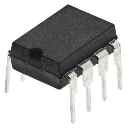
| 描述 | IC OFF-LINE PWR-SUP CNTRLR 8-DIP交流/直流转换器 Off-Line Cntlr |
| DevelopmentKit | UCC3889EVM |
| 产品分类 | |
| 品牌 | Texas Instruments |
| 产品手册 | |
| 产品图片 |
|
| rohs | 符合RoHS无铅 / 符合限制有害物质指令(RoHS)规范要求 |
| 产品系列 | 电源管理 IC,交流/直流转换器,Texas Instruments UCC3889N- |
| 数据手册 | |
| 产品型号 | UCC3889N |
| 产品目录页面 | |
| 产品种类 | 交流/直流转换器 |
| 供应商器件封装 | 8-PDIP |
| 其它名称 | 296-11534-5 |
| 功率(W) | - |
| 包装 | 管件 |
| 单位重量 | 523.200 mg |
| 占空比-最大 | 55 % |
| 商标 | Texas Instruments |
| 安装风格 | Through Hole |
| 封装 | Tube |
| 封装/外壳 | 8-DIP(0.300",7.62mm) |
| 封装/箱体 | PDIP-8 |
| 工作温度 | 0°C ~ 70°C |
| 工作温度范围 | 0 C to + 70 C |
| 工厂包装数量 | 50 |
| 开关频率 | 250 kHz |
| 拓扑结构 | Flyback |
| 标准包装 | 50 |
| 电压-击穿 | - |
| 电压-输入 | 6 V ~ 9.3 V |
| 电压-输出 | 20V |
| 电源电流 | 1.2 mA |
| 类型 | Voltage Mode PWM Controllers |
| 系列 | UCC3889 |
| 绝缘 | Non-Isolated |
| 输入/电源电压—最大值 | 9.3 V |
| 输入/电源电压—最小值 | 6.6 V |
| 输出电压 | 12 V, 18 V |
| 输出电流 | 100 mA |
| 输出端数量 | 1 Output |
| 输出隔离 | 非隔离 |
| 配用 | /product-detail/zh/UCC3889EVM/296-13598-ND/486556 |
| 频率范围 | - |


- 商务部:美国ITC正式对集成电路等产品启动337调查
- 曝三星4nm工艺存在良率问题 高通将骁龙8 Gen1或转产台积电
- 太阳诱电将投资9.5亿元在常州建新厂生产MLCC 预计2023年完工
- 英特尔发布欧洲新工厂建设计划 深化IDM 2.0 战略
- 台积电先进制程称霸业界 有大客户加持明年业绩稳了
- 达到5530亿美元!SIA预计今年全球半导体销售额将创下新高
- 英特尔拟将自动驾驶子公司Mobileye上市 估值或超500亿美元
- 三星加码芯片和SET,合并消费电子和移动部门,撤换高东真等 CEO
- 三星电子宣布重大人事变动 还合并消费电子和移动部门
- 海关总署:前11个月进口集成电路产品价值2.52万亿元 增长14.8%


.jpg)
PDF Datasheet 数据手册内容提取
UCC1889 UCC2889 UCC3889 Off-line Power Supply Controller FEATURES DESCRIPTION • Transformerless Off-line The UCC1889 controller is optimized for use as an off-line, low power, low voltage, Applications regulated bias supply. The unique circuit topology utilized in this device can be visualized as two cascaded flyback converters, each operating in the discontinu- • Ideal Primary-side Bias Supply ous mode, and both driven from a single external power switch. The significant • Efficient BiCMOS Design benefit of this approach is the ability to achieve voltage conversion ratios of 400V to 12V with no transformer and low internal losses. • Wide Input Range The control algorithm utilized by the UCC1889 is to force the switch on time to be • Fixed or Adjustable inversely proportional to the input line voltage while the switch off time is made in- Low Voltage Output versely proportional to the output voltage. This action is automatically controlled by • Uses Low Cost SMD Inductors an internal feedback loop and reference. The cascaded configuration allows a volt- age conversion from 400V to 12V to be achieved with a switch duty cycle greater • Short Circuit Protected than 10%. This topology also offers inherent short circuit protection since as the • Optional Isolation Capability output voltage falls to zero, the switch off time approaches infinity. The output voltage can be easily set to 12V or 18V. Moreover, it can be pro- grammed for other output voltages less than 18V with a few additional compo- nents. An isolated version can be achieved with this topology as described further in Unitrode Application Note U-149. OPERATION With reference to the application diagram below, when input voltage is first applied, the RON current into TON is directed to VCC where it charges the external capacitor, C3, connected to VCC. As voltage builds on VCC, an internal undervoltage lockout holds the circuit off and the output at DRIVE low until VCC reaches 8.4V. At this time, DRIVE goes high turning on the power switch, Q1, and redirecting the current into TON to the timing capacitor, CT. CT charges to a fixed threshold with a current ICHG=0.8 • (VIN - 4.5V)/RON. Since DRIVE will only be high for as long as CT charges, the power switch on time will be inversely proportional to line voltage. This provides a constant line voltage-switch on time product. TYPICAL APPLICATION Note: This device incorporates patented technology used under license from Lambda Electronics, Inc. UDG-93060-1 SLUS158A - FEBRUARY 1995 - REVISED FEBRUARY 2003
UCC1889 UCC2889 UCC3889 OPERATION (cont.) At the end of the on time, Q1 is turned off and the RON IDCHG = (VOUT - 0.7V) / ROFF current into TON is again diverted to VCC. Thus the cur- As VOUT increases, IDCHG increases resulting in the rent through RON, which charges CT during the on time, reduction of off time. The frequency of operation in- contributes to supplying control power during the off time. creases and VOUT rises quickly to its regulated value. The power switch off time is controlled by the discharge 3. In this region, a transconductance amplifier reduces of CT which, in turn, is programmed by the regulated out- IDCHG in order to maintain VOUT in regulation. put voltage. The relationship between CT discharge cur- rent, IDCHG, and output voltage is illustrated as follows: 4. If VOUT should rise above its regulation range, IDCHG falls to zero and the circuit returns to the minimum fre- quency established by RS and CT. The range of switching frequencies is established by RON, ROFF, RS, and CT as follows: Frequency = 1/(TON + TOFF) TON = RON • CT • 4.6 V/(VIN - 4.5V) TOFF (max) = 1.4 • RS • CT Regions 1 and 4 1. When VOUT = 0, the off time is infinite. This feature TOFF = ROFF • CT • 3.7V /(VOUT - 0.7V) provides inherent short circuit protection. However, to Region 2, excluding the effects of RS ensure output voltage startup when the output is not a which have a minimal impact on TOFF. short, a high value resistor, RS, is placed in parallel The above equations assume that VCC equals 9V. The with CT to establish a minimum switching frequency. voltage at TON increases from approximately 2.5V to 2. As VOUT rises above approximately 0.7V to its regu- 6.5V while CT is charging. To take this into account, VIN lated value, IDCHG is defined by ROFF, and therefore is is adjusted by 4.5V in the calculation of TON. The voltage equal to: at TOFF is approximately 0.7V. DESIGN EXAMPLE The UCC3889 regulates a 12 volt, 1 Watt nonisolated DC output from AC inputs between 80 and 265 volts. In this ex- ample, the IC is programmed to deliver a maximum on time gate drive pulse width of 2.4 microseconds which occurs at 80 VAC. The corresponding switching frequency is approximately 100kHz at low line, and overall efficiency is ap- proximately 50%. Additional design information is available in Unitrode Application Note U-149. UDG-93062-3 2
UCC1889 UCC2889 UCC3889 ABSOLUTE MAXIMUM RATINGS CONNECTION DIAGRAM ICC. . . . . . . . . . . . . . . . . . . . . . . . . . . . . . . . . . . . . . . . . . . . 5mA DIL-8, SOIC-8 (Top View) Current into TON Pin. . . . . . . . . . . . . . . . . . . . . . . . . . . . . 1.5mA N or J, D Package Voltage on VOUT Pin. . . . . . . . . . . . . . . . . . . . . . . . . . . . . . . 20V Current into TOFF Pin . . . . . . . . . . . . . . . . . . . . . . . . . . . . 250m A Storage Temperature. . . . . . . . . . . . . . . . . . . . -65(cid:176) C to +150(cid:176) C Note: Unless otherwise indicated, voltages are referenced to ground and currents are positive into, negative out of, the speci- fied terminals. ELECTRICAL CHARACTERISTICS Unless otherwise stated, these specifications hold for TA = 0(cid:176) C to 70(cid:176) C for the UCC3889, -40(cid:176) C to +85(cid:176) C for the UCC2889, and -55(cid:176) C to +125(cid:176) C for the UCC1889. No load at DRIVE pin (CLOAD=0). PARAMETER TEST CONDITIONS MIN TYP MAX UNITS General VCC Zener Voltage ICC < 1.5mA 8.6 9.0 9.3 V Startup Current VOUT = 0 150 250 m A Operating Current I(VOUT) VOUT = 11V, F = 150kHz 1.2 2.5 mA Under-Voltage-Lockout Start Threshold VOUT = 0 8.0 8.4 8.8 V Minimum Operating Voltage after Start VOUT = 0 6.0 6.3 6.6 V Hysteresis VOUT = 0 1.8 V Oscillator Amplitude VCC = 9V 3.5 3.7 3.9 V CT to DRIVE high Propagation Delay Overdrive = 0.2V 100 200 ns CT to DRIVE low Propagation Delay Overdrive = 0.2V 50 100 ns Driver VOL I = 20mA, VCC = 9V 0.15 0.4 V I = 100mA, VCC = 9V 0.7 1.8 V VOH I = - 20mA, VCC = 9V 8.5 8.8 V I = - 100mA, VCC = 9V 6.1 7.8 V Rise Time CLOAD = 1nF 35 70 ns Fall Time CLOAD = 1nF 30 60 ns Line Voltage Detection Charge Coefficient: ICHG / I(TON) VCT = 3V, DRIVE = High, I(TON) = 1mA 0.73 0.79 0.85 Minimum Line Voltage for Fault RON = 330k 60 80 100 V Minimum Current I(TON) for Fault RON = 330k 220 m A On Time During Fault CT = 150pF, VLINE = Min - 1V 2 m s Oscillator Restart Delay after Fault 0.5 ms VOUT Error Amp VOUT Regulated 12V (ADJ Open) VCC = 9V, IDCHG = I(TOFF)/2 11.2 11.9 12.8 V VOUT Regulated 18V (ADJ = 0V) VCC = 9V, IDCHG = I(TOFF)/2 16.5 17.5 19.5 V Discharge Ratio: IDCHG / I(TOFF) I(TOFF) = 50m A 0.93 1.00 1.07 Voltage at TOFF I(TOFF) = 50m A 0.6 0.95 1.3 V Regulation gm (Note 1) Max IDCHG = 50m A 1.0 mA/V Max IDCHG = 125m A 0.8 1.7 2.9 mA/V D IDCHG Note 1:gm is defined as D VOUT for the values of VOUT when VOUT is in regulation. The two points used to calculate gm are for IDCHG at 65% and 35% of its maximum value. 3
UCC1889 UCC2889 UCC3889 PIN DESCRIPTIONS ADJ: The ADJ pin is used to provide a 12V or an 18V resistor connected between VOUT and TOFF. regulated supply without additional external components. TON (line voltage control): TON serves three functions. To select the 12V option, ADJ pin is left open. To select When CT is discharging (off time), the current through the 18V option, ADJ pin must be grounded. For other out- TON is routed to VCC. When CT is charging (on time), the put voltages less than 18V, a resistor divider between current through TON is split 80% to set the CT charge VOUT, ADJ and GND is needed. Note, however, that for time and 20% to sense minimum line voltage which oc- output voltages less than VCC, the device needs addi- curs for a TON current of 220m A. For a minimum line volt- tional bootstrapping to VCC from an external source such age of 80V, RON is 330kW . as the line voltage. If so, precautions must be taken to ensure that total ICC does not exceed 5mA. The CT voltage slightly affects the value of the charge current during the on time. During this time, the voltage at CT (timing capacitor): The signal voltage across CT has the TON pin increases from approximately 2.5V to 6.5V. a peak-to-peak swing of 3.7V for 9V VCC. As the voltage on CT crosses the oscillator upper threshold, DRIVE goes VCC (chip supply voltage): The supply voltage of the low. As the voltage on CT crosses the oscillator lower device at pin VCC is internally clamped at 9V. Normally, threshold, DRIVE goes high. VCC is not directly powered from an external voltage source such as the line voltage. In the event that VCC is DRIVE: This output is a CMOS stage capable of sinking directly connected to a voltage source for additional boot- 200mA peak and sourcing 150mA peak. The output volt- strapping, precautions must be taken to ensure that total age swing is 0 to VCC. ICC does not exceed 5mA. GND (chip ground): All voltages are measured with re- VOUT (regulated output): The VOUT pin is directly con- spect to GND. nected to the power supply output voltage. When VOUT is TOFF (regulated output control): TOFF sets the dis- greater than VCC, VOUT bootstraps VCC. charge current of the timing capacitor through an external BLOCK DIAGRAM UDG-93064-2 4
UCC1889 UCC2889 UCC3889 TYPICAL WAVEFORMS 5
UCC1889 UCC2889 UCC3889 UNITRODE INTEGRATED CIRCUITS 7 CONTINENTAL BLVD. • MERRIMACK, NH 03054 TEL. 603-424-2410 • FAX 603-424-3460 6
PACKAGE OPTION ADDENDUM www.ti.com 6-Feb-2020 PACKAGING INFORMATION Orderable Device Status Package Type Package Pins Package Eco Plan Lead/Ball Finish MSL Peak Temp Op Temp (°C) Device Marking Samples (1) Drawing Qty (2) (6) (3) (4/5) UCC2889D ACTIVE SOIC D 8 75 Green (RoHS NIPDAU Level-2-260C-1 YEAR -40 to 85 UCC2889 & no Sb/Br) UCC2889DTR ACTIVE SOIC D 8 2500 Green (RoHS NIPDAU Level-2-260C-1 YEAR -40 to 85 UCC2889 & no Sb/Br) UCC2889DTRG4 ACTIVE SOIC D 8 2500 Green (RoHS NIPDAU Level-2-260C-1 YEAR -40 to 85 UCC2889 & no Sb/Br) UCC2889N ACTIVE PDIP P 8 50 Green (RoHS NIPDAU N / A for Pkg Type -40 to 85 UCC2889N & no Sb/Br) UCC3889D ACTIVE SOIC D 8 75 Green (RoHS NIPDAU Level-2-260C-1 YEAR 0 to 70 UCC3889 & no Sb/Br) UCC3889DG4 ACTIVE SOIC D 8 75 Green (RoHS NIPDAU Level-2-260C-1 YEAR 0 to 70 UCC3889 & no Sb/Br) UCC3889DTR ACTIVE SOIC D 8 2500 Green (RoHS NIPDAU Level-2-260C-1 YEAR 0 to 70 UCC3889 & no Sb/Br) UCC3889N ACTIVE PDIP P 8 50 Green (RoHS NIPDAU N / A for Pkg Type 0 to 70 UCC3889N & no Sb/Br) (1) The marketing status values are defined as follows: ACTIVE: Product device recommended for new designs. LIFEBUY: TI has announced that the device will be discontinued, and a lifetime-buy period is in effect. NRND: Not recommended for new designs. Device is in production to support existing customers, but TI does not recommend using this part in a new design. PREVIEW: Device has been announced but is not in production. Samples may or may not be available. OBSOLETE: TI has discontinued the production of the device. (2) RoHS: TI defines "RoHS" to mean semiconductor products that are compliant with the current EU RoHS requirements for all 10 RoHS substances, including the requirement that RoHS substance do not exceed 0.1% by weight in homogeneous materials. Where designed to be soldered at high temperatures, "RoHS" products are suitable for use in specified lead-free processes. TI may reference these types of products as "Pb-Free". RoHS Exempt: TI defines "RoHS Exempt" to mean products that contain lead but are compliant with EU RoHS pursuant to a specific EU RoHS exemption. Green: TI defines "Green" to mean the content of Chlorine (Cl) and Bromine (Br) based flame retardants meet JS709B low halogen requirements of <=1000ppm threshold. Antimony trioxide based flame retardants must also meet the <=1000ppm threshold requirement. (3) MSL, Peak Temp. - The Moisture Sensitivity Level rating according to the JEDEC industry standard classifications, and peak solder temperature. (4) There may be additional marking, which relates to the logo, the lot trace code information, or the environmental category on the device. Addendum-Page 1
PACKAGE OPTION ADDENDUM www.ti.com 6-Feb-2020 (5) Multiple Device Markings will be inside parentheses. Only one Device Marking contained in parentheses and separated by a "~" will appear on a device. If a line is indented then it is a continuation of the previous line and the two combined represent the entire Device Marking for that device. (6) Lead/Ball Finish - Orderable Devices may have multiple material finish options. Finish options are separated by a vertical ruled line. Lead/Ball Finish values may wrap to two lines if the finish value exceeds the maximum column width. Important Information and Disclaimer:The information provided on this page represents TI's knowledge and belief as of the date that it is provided. TI bases its knowledge and belief on information provided by third parties, and makes no representation or warranty as to the accuracy of such information. Efforts are underway to better integrate information from third parties. TI has taken and continues to take reasonable steps to provide representative and accurate information but may not have conducted destructive testing or chemical analysis on incoming materials and chemicals. TI and TI suppliers consider certain information to be proprietary, and thus CAS numbers and other limited information may not be available for release. In no event shall TI's liability arising out of such information exceed the total purchase price of the TI part(s) at issue in this document sold by TI to Customer on an annual basis. Addendum-Page 2
PACKAGE MATERIALS INFORMATION www.ti.com 26-Jan-2013 TAPE AND REEL INFORMATION *Alldimensionsarenominal Device Package Package Pins SPQ Reel Reel A0 B0 K0 P1 W Pin1 Type Drawing Diameter Width (mm) (mm) (mm) (mm) (mm) Quadrant (mm) W1(mm) UCC2889DTR SOIC D 8 2500 330.0 12.4 6.4 5.2 2.1 8.0 12.0 Q1 UCC3889DTR SOIC D 8 2500 330.0 12.4 6.4 5.2 2.1 8.0 12.0 Q1 PackMaterials-Page1
PACKAGE MATERIALS INFORMATION www.ti.com 26-Jan-2013 *Alldimensionsarenominal Device PackageType PackageDrawing Pins SPQ Length(mm) Width(mm) Height(mm) UCC2889DTR SOIC D 8 2500 367.0 367.0 35.0 UCC3889DTR SOIC D 8 2500 367.0 367.0 35.0 PackMaterials-Page2
None
PACKAGE OUTLINE D0008A SOIC - 1.75 mm max height SCALE 2.800 SMALL OUTLINE INTEGRATED CIRCUIT C SEATING PLANE .228-.244 TYP [5.80-6.19] .004 [0.1] C A PIN 1 ID AREA 6X .050 [1.27] 8 1 2X .189-.197 [4.81-5.00] .150 NOTE 3 [3.81] 4X (0 -15 ) 4 5 8X .012-.020 B .150-.157 [0.31-0.51] .069 MAX [3.81-3.98] .010 [0.25] C A B [1.75] NOTE 4 .005-.010 TYP [0.13-0.25] 4X (0 -15 ) SEE DETAIL A .010 [0.25] .004-.010 0 - 8 [0.11-0.25] .016-.050 [0.41-1.27] DETAIL A (.041) TYPICAL [1.04] 4214825/C 02/2019 NOTES: 1. Linear dimensions are in inches [millimeters]. Dimensions in parenthesis are for reference only. Controlling dimensions are in inches. Dimensioning and tolerancing per ASME Y14.5M. 2. This drawing is subject to change without notice. 3. This dimension does not include mold flash, protrusions, or gate burrs. Mold flash, protrusions, or gate burrs shall not exceed .006 [0.15] per side. 4. This dimension does not include interlead flash. 5. Reference JEDEC registration MS-012, variation AA. www.ti.com
EXAMPLE BOARD LAYOUT D0008A SOIC - 1.75 mm max height SMALL OUTLINE INTEGRATED CIRCUIT 8X (.061 ) [1.55] SYMM SEE DETAILS 1 8 8X (.024) [0.6] SYMM (R.002 ) TYP [0.05] 5 4 6X (.050 ) [1.27] (.213) [5.4] LAND PATTERN EXAMPLE EXPOSED METAL SHOWN SCALE:8X SOLDER MASK SOLDER MASK METAL OPENING OPENING METAL UNDER SOLDER MASK EXPOSED METAL EXPOSED METAL .0028 MAX .0028 MIN [0.07] [0.07] ALL AROUND ALL AROUND NON SOLDER MASK SOLDER MASK DEFINED DEFINED SOLDER MASK DETAILS 4214825/C 02/2019 NOTES: (continued) 6. Publication IPC-7351 may have alternate designs. 7. Solder mask tolerances between and around signal pads can vary based on board fabrication site. www.ti.com
EXAMPLE STENCIL DESIGN D0008A SOIC - 1.75 mm max height SMALL OUTLINE INTEGRATED CIRCUIT 8X (.061 ) [1.55] SYMM 1 8 8X (.024) [0.6] SYMM (R.002 ) TYP [0.05] 5 4 6X (.050 ) [1.27] (.213) [5.4] SOLDER PASTE EXAMPLE BASED ON .005 INCH [0.125 MM] THICK STENCIL SCALE:8X 4214825/C 02/2019 NOTES: (continued) 8. Laser cutting apertures with trapezoidal walls and rounded corners may offer better paste release. IPC-7525 may have alternate design recommendations. 9. Board assembly site may have different recommendations for stencil design. www.ti.com
IMPORTANTNOTICEANDDISCLAIMER TI PROVIDES TECHNICAL AND RELIABILITY DATA (INCLUDING DATASHEETS), DESIGN RESOURCES (INCLUDING REFERENCE DESIGNS), APPLICATION OR OTHER DESIGN ADVICE, WEB TOOLS, SAFETY INFORMATION, AND OTHER RESOURCES “AS IS” AND WITH ALL FAULTS, AND DISCLAIMS ALL WARRANTIES, EXPRESS AND IMPLIED, INCLUDING WITHOUT LIMITATION ANY IMPLIED WARRANTIES OF MERCHANTABILITY, FITNESS FOR A PARTICULAR PURPOSE OR NON-INFRINGEMENT OF THIRD PARTY INTELLECTUAL PROPERTY RIGHTS. These resources are intended for skilled developers designing with TI products. You are solely responsible for (1) selecting the appropriate TI products for your application, (2) designing, validating and testing your application, and (3) ensuring your application meets applicable standards, and any other safety, security, or other requirements. These resources are subject to change without notice. TI grants you permission to use these resources only for development of an application that uses the TI products described in the resource. Other reproduction and display of these resources is prohibited. No license is granted to any other TI intellectual property right or to any third party intellectual property right. TI disclaims responsibility for, and you will fully indemnify TI and its representatives against, any claims, damages, costs, losses, and liabilities arising out of your use of these resources. TI’s products are provided subject to TI’s Terms of Sale (www.ti.com/legal/termsofsale.html) or other applicable terms available either on ti.com or provided in conjunction with such TI products. TI’s provision of these resources does not expand or otherwise alter TI’s applicable warranties or warranty disclaimers for TI products. Mailing Address: Texas Instruments, Post Office Box 655303, Dallas, Texas 75265 Copyright © 2020, Texas Instruments Incorporated