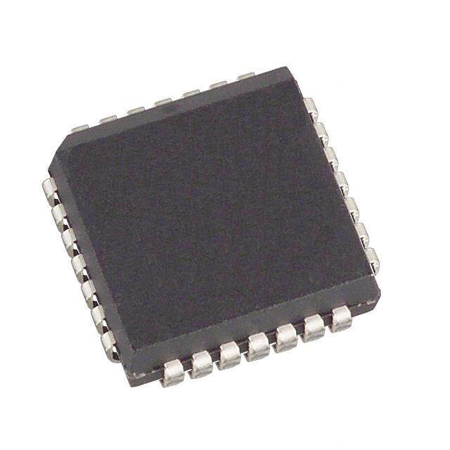
- 型号: UCC3750N
- 制造商: Texas Instruments
- 库位|库存: xxxx|xxxx
- 要求:
| 数量阶梯 | 香港交货 | 国内含税 |
| +xxxx | $xxxx | ¥xxxx |
查看当月历史价格
查看今年历史价格
UCC3750N产品简介:
ICGOO电子元器件商城为您提供UCC3750N由Texas Instruments设计生产,在icgoo商城现货销售,并且可以通过原厂、代理商等渠道进行代购。 UCC3750N价格参考¥询价-¥询价。Texas InstrumentsUCC3750N封装/规格:接口 - 电信, Telecom IC Ring Generator Controller 28-PDIP。您可以下载UCC3750N参考资料、Datasheet数据手册功能说明书,资料中有UCC3750N 详细功能的应用电路图电压和使用方法及教程。
| 参数 | 数值 |
| 产品目录 | 集成电路 (IC)半导体 |
| 描述 | IC SOURCE RINGER CNTRLR 28-DIP电话振铃器 Source Ringer Controller |
| 产品分类 | |
| 品牌 | Texas Instruments |
| 产品手册 | |
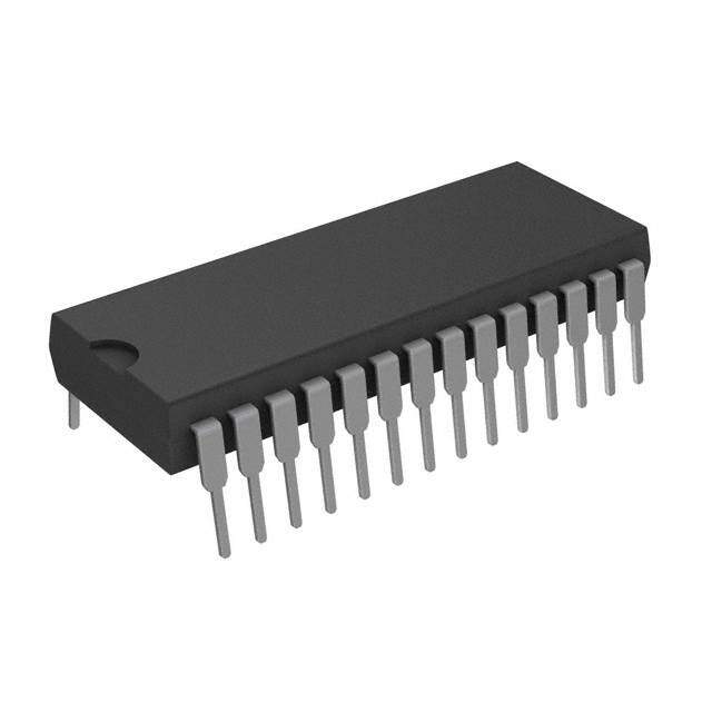
| 产品图片 |
|
| rohs | 符合RoHS无铅 / 符合限制有害物质指令(RoHS)规范要求 |
| 产品系列 | 通信及网络 IC,电话振铃器,Texas Instruments UCC3750N- |
| 数据手册 | 点击此处下载产品Datasheethttp://www.ti.com/lit/pdf/mpdi008 |
| 产品型号 | UCC3750N |
| 产品 | Telecom Ringer |
| 产品目录页面 | |
| 产品种类 | 电话振铃器 |
| 供应商器件封装 | 28-PDIP |
| 其它名称 | 296-11454-5 |
| 功率(W) | - |
| 功能 | 铃声发生器控制器 |
| 包括 | DC 电流限制,次级侧电压模式控制 |
| 包装 | 管件 |
| 商标 | Texas Instruments |
| 安装类型 | 通孔 |
| 安装风格 | Through Hole |
| 封装 | Tube |
| 封装/外壳 | 28-DIP(0.600",15.24mm) |
| 封装/箱体 | PDIP-28 |
| 工作温度 | 0°C ~ 70°C |
| 工作电源电压 | 5 V |
| 工厂包装数量 | 13 |
| 接口 | - |
| 最大工作温度 | + 70 C |
| 最小工作温度 | 0 C |
| 标准包装 | 13 |
| 电压-电源 | 5V |
| 电流-电源 | 500µA |
| 电路数 | 1 |
| 类型 | Multiple |
| 系列 | UCC3750 |
| 频率 | 20 Hz, 25 Hz, 50 Hz |



- 商务部:美国ITC正式对集成电路等产品启动337调查
- 曝三星4nm工艺存在良率问题 高通将骁龙8 Gen1或转产台积电
- 太阳诱电将投资9.5亿元在常州建新厂生产MLCC 预计2023年完工
- 英特尔发布欧洲新工厂建设计划 深化IDM 2.0 战略
- 台积电先进制程称霸业界 有大客户加持明年业绩稳了
- 达到5530亿美元!SIA预计今年全球半导体销售额将创下新高
- 英特尔拟将自动驾驶子公司Mobileye上市 估值或超500亿美元
- 三星加码芯片和SET,合并消费电子和移动部门,撤换高东真等 CEO
- 三星电子宣布重大人事变动 还合并消费电子和移动部门
- 海关总署:前11个月进口集成电路产品价值2.52万亿元 增长14.8%
PDF Datasheet 数据手册内容提取
application UCC2750 INFO UCC3750 available Source Ringer Controller FEATURES DESCRIPTION • ProvidesControlforFlybackBased The UCC3750 Source Ringer Controller provides a complete control and FourQuadrantAmplifierTopology drive solution for a four quadrant flyback-based ring generator circuit. The ICcontrolsaprimarysideswitch,whichismodulatedwhenpowertransfer • OnboardSineWaveReferencewith is taking place from input to output. It also controls two secondary LowTHD switches which act as synchronous rectifier switches during positive • SelectableRingingFrequencyfor power flow. These switches are pulse-width-modulated when the power is DifferentPhoneSystems(20Hz, beingdeliveredbacktothesource. 25Hzand50Hz) The UCC3750 has an onboard sine wave reference with programmable • ProgrammableOutputAmplitudeand frequencies of 20Hz, 25Hz and 50Hz. The reference is derived from a DCOffset high-frequency (32kHz) crystal connected externally. Two fre- • DCCurrentLimitingforShortCircuit quency-selectpinscontrolaninternaldividertogiveasinusoidaloutputat Protection 20Hz, 25Hz or 50Hz. The ring generator can also be used at other fre- quencies by supplying externally generated sine-waves to the chip or by • SecondarySideVoltageMode clockingthecrystalinputatafixedmultipleofthedesiredfrequency. Control Other features included in the UCC3750 are programmable DC current • OperatesfromaSingle5VSupply limit(withbufferamplifier),acharge-pumpcircuitforgatedrivevoltage,in- ternal 3V and 7.5V references, a triangular clock oscillator and a buffer amplifier for adding programmable DC offset to the output voltage. The UCC3750 also provides an uncommitted amplifier (AMP) for other signal processingrequirements. TYPICAL APPLICATION 0V VOUT –48V 4V8INV VOUT 28 26 27 25 GD2 GD3 ENBL REF VCP 4 2 GD1 UCC3750 VS2 6 24 RT 23 CT VS1 5 1 RGOOD VDD 7 5V 11 OUTDC OUT2 15 12 NEGDC 13 AMPOUT NEG2 18 14 AMPIN 22 XTAL1 OUT1 16 21 XTAL2 NEG1 17 20 FS0 SINFLT 10 19 FS1 SINREF SWRLY GND 9 8 3 C17 0.047µF UDG-99073 SLUS172C-DECEMBER1999-REVISEDAUGUST2005
UCC2750 UCC3750 ABSOLUTE MAXIMUM RATINGS CONNECTION DIAGRAM InputSupplyVoltage DIL-28,SOIC-28(TopView) VDD ........................................7.5V NPackage,DWPackage MaximumForcedVoltage VCP ................................–0.3Vto13.2V VS1,VS2...............................–0.3Vto5V RGOOD 1 28 GD2 OUT1,OUT2,AMPOUT,OUTDC GD1 2 27 ENBL MaximumForcedVoltage ................–0.3Vto7.5V MaximumForcedCurrent..............InternallyLimited GND 3 26 GD3 NEG1,NEG2,AMPIN,NEGDC MaximumForcedVoltage ................–0.3Vto7.5V VCP 4 25 REF SINREF,SINFLT VS1 5 24 RT MaximumForcedVoltage ................–0.3Vto7.5V LogicInputs VS2 6 23 CT MaximumForcedVoltage ................–0.3Vto7.5V VDD 7 22 XTAL1 ReferenceOutputCurrent(REF) ..........InternallyLimited OutputCurrent(GD1,GD2,GD3) SWRLY 8 21 XTAL2 Pulsed.......................................1.5A SINREF 9 20 FS0 StorageTemperature...................–65°Cto+150°C JunctionTemperature...................–55°Cto+150°C SINFLT 10 19 FS1 LeadTemperature(Soldering,10Sec.).............+300°C OUTDC 11 18 NEG2 Unless otherwise indicated, voltages are reference to ground NEGDC 12 17 NEG1 andcurrentsarepositiveinto,negativeoutofthespecifiedter- minal. Pulsed is defined as a less than 10% duty cycle with a AMPOUT 13 16 OUT1 maximum duration of 500ns. Consult Packaging Section of AMPIN 14 15 OUT2 Databook for thermal limitations and considerations of pack- ages. ELECTRICAL CHARACTERISTICS:Unlessotherwisestated,thesespecificationsapplyforT =0°Cto70°Cforthe A UCC3750,–40°Cto+85°CfortheUCC2750,RT=14k,CT=470pF,C =0.1µF,FS0=0,FS1=0,VDD=5V.T =T . REF A J PARAMETER TESTCONDITIONS MIN TYP MAX UNITS VDDSupply SupplyCurrent-Active With12VSuppliedtoV andChargePump 0.5 1 mA CP Disabled InternalReferencew/ExternalBypass OutputVoltage(REF) 7.3 7.55 7.8 V LoadRegulation I =0mA–2mA 30 60 mV REF LineRegulation VCP=10Vto13V,I =1mA 3 15 mV REF Amplifier InputVoltage Error,DCOffsetandAmpAmplifiers 2.9 3 3.1 V DCLimitAmplifier 0.7125 0.75 0.7875 V InputBiasCurrent 15 100 nA AVOL V =2Vto4V 70 dB OUT VOH Source100µA 5.35 6 7.0 V VOL Sink100µA 0.2 0.65 V ShortCircuitCurrent V =0Vand5VwithV =0Vand5V 0.5 2 3 mA IN OUT SineReference Accuracy T =25°C,ProgramFrequency–Reference –1 0 1 Hz J Frequency TotalHarmonicDistortion (Note1) 2 % Amplitude Peak 0.475 0.5 0.525 V Offset 2.85 3.0 3.15 V 2
UCC2750 UCC3750 ELECTRICAL CHARACTERISTICS:Unlessotherwisestated,thesespecificationsapplyforT =0°Cto70°Cforthe A UCC3750,–40°Cto+85°CfortheUCC2750,RT=14k,CT=470pF,C =0.1µF,FS0=0,FS1=0,VDD=5V.T =T . REF A J PARAMETER TESTCONDITIONS MIN TYP MAX UNITS Oscillator Accuracy 108 128 148 kHz PeakVoltage 4.6 4.75 4.9 V ValleyVoltage 2.9 3.05 3.2 V ChargePump SwitchPullUpResistance(VS1,VS2) 10 30 Ω SwitchPullDownResistance(VS1,VS2) 10 30 Ω OutputVoltage(VCP) VDD=5V,I =10mA 11 12 14 V VCP OutputDrivers PullUpResistance 9 15 Ω PullDownResistance 9 15 Ω RiseTime CL=2.7nF 50 100 ns FallTime CL=2.7nF 50 100 ns CurrentLimit DCLimitThresholdVoltagePositive R5/R6=3 0.4 0.5 0.6 V DCLimitThresholdVoltageNegative R5/R6=3 –0.6 –0.5 –0.4 V DutyCycle MaximumPWMDutyCycle 48 50 % RectifierDutyCycle 50 % Note1:GuaranteedbymeasuringthestepsofthePWLSineWave. STATE %VCC VALUEFORREF=7.5 STATE %VCC VALUEFORREF=7.5 0 0.3333 2.5 5 0.4255 3.191 1 0.3384 2.538 6 0.4471 3.353 2 0.3528 2.646 7 0.4616 3.462 3 0.3745 2.808 8 0.4666 3.5 4 0.4 3 PIN DESCRIPTIONS AMPIN:Invertinginputoftheuncommittedamplifier. TableI.Frequencyselectiontable AMPOUT:Outputoftheuncommittedamplifier. (for32kHzcrystal). CT: This pin programs the internal PWM oscillator FS0 FS1 SINREF(Hz) frequency. Capacitor from CT to GND sets the charge 0 0 20 1 0 25 anddischargetimeoftheoscillator. 0 1 50 ENBL: Logic input which enables the outputs and the 1 1 HighImpedance charge pump when high. ENBL should be pulled low to turntheoutputsoff. GD1: Output driver that controls the primary side switch FS0, FS1: Frequency select pins for the internal in a flyback converter through a gate drive transformer. sine-wave generator. Table 1 provides the SINREF The output signal on this pin is PWM during positive frequencies as a function of FS0 and FS1 when a 32kHz power transfer modes and zero during negative power crystal is used at the crystal inputs (XTAL1, XTAL2). transfermodes. Other proportional frequencies can be obtained with a differentcrystal.InputsFS0andFS1areTTLcompatible. 3
UCC2750 UCC3750 PIN DESCRIPTIONS (cont.) GD2:Outputdriverthatcontrolsthep-channelsecondary REF:Internal 7.5V reference. For best results, bypass to side switch in the flyback converter. The output signal on GNDwithaceramiccapacitor(>0.1µF). this pin is PWM during mode 4 (Fig. 2) when the RGOOD: Logic output that indicates that the error reference signal is negative and power is being returned amplifier output is within range (0< D< 0.5). This pin can to the input. This pin functions as a synchronous rectifier sourceupto0.5mAofcurrent. output during mode 1 with positive reference signal and positivepowertransfer.Thisoutputislogicallyinvertedto RT: Resistor from RT to GND helps set the oscillator provide the correct polarity drive signal for a p-channel frequency. RT programs the charge and discharge switch. currentsofCT. GD3:Outputdriverthatcontrolsthen-channelsecondary SINFLT: This signal is the buffered version of SINREF. side switch in the flyback converter. The output signal on This signal is summed with the DC offset level with this pin is PWM during mode 2 (Fig. 2) when the appropriatescaling. reference signal is positive and power is being returned SINREF: This pin is the output of the sine-wave to the input. This pin functions as a synchronous rectifier reference generator. It has a high output impedance output during mode 3 with a negative reference signal (≈25kΩ). A0.01µF capacitor to GND is recommended to andpositivepowertransfer. provide smoothing of the sinewave. When FS0 and FS1 GND: Reference point for the internal reference and all are both set high, the sine reference generator is thresholds. Also provides the signal return path for all disabled allowing this pin to accept an external sinewave otherpins. input. NEG1: Inverting input of the buffer amplifier that acts as SWRLY: Logic output that leads the battery offset a summing junction for the DC (battery) offset voltage crossings (by typically 5ms) to allow “zero voltage” relay andsinewavereference. switching.Thispincantypicallysource250µA. NEG2: Inverting input of the error amplifier where the XTAL1:Crystal connection for external crystal. This pin ringer output voltage and the reference signal with the can be also used to clock the internal sine wave desired offset are applied with a weighted sum. generatorwhenXTAL2isconnectedtoVDD/2. Feedback compensation is connected between NEG2 XTAL2:Crystalconnectionforexternalcrystal. andOUT2. VCP: External connection for charge pump storage NEGDC: Inverting input of the amplifier used for DC capacitor. A capacitance ≥2.2mF is recommended for currentlimiting. low charge pump output ripple. The voltage at this pin is OUT1:Outputofthebufferamplifierthatprovidesscaling used by the output drivers for gate drive voltages. and filtering for the reference signal before feeding it into Alternatively, a regulated gate drive voltage (>10V) can the error amplifier. This output is also used internally to be connected at this pin while leaving the charge pump selectthePWMmodefortheflybackconverter. circuitatnodesVS1,VS2disconnected. OUT2: Output of the error amplifier. Used to connect VDD: External supply input used to bias internal logic compensation components. This output’s absolute value functions. Typically a regulated 5V supply is connected determinesthedutycycleofthePWMpulse.Thepolarity between this pin and GND. It also is the input voltage for ofthissignalalsodeterminesthePWMmode. the voltage tripler circuit to generate the gate drive voltage. OUTDC:Output of the DC current limit amplifier. The DC current limit is activated when this pin is above 4.5V or VS1, VS2: Voltage switches for the voltage tripler below1.5V. (charge pump circuit). They provide different voltage levels to external capacitors in order to pump up the voltagefromVDDtoVCP. 4
UCC2750 UCC3750 DETAILED BLOCK DIAGRAM SWRLY FS0 FS1 SINREF SINFLT NEG1 OUT1 NEG2 OUT2 8 20 19 9 10 17 16 18 15 REF XTAL1 22 REF REF XTAL XTAL2 21 OSC SINGEERNEEFREARTEONRCE – – FULLWAVE MAG VCM + VCM + RECTIFIER SIGN AMPOUT 13 ERROR DCOFFSETAMP AMP AMPIN 14 – AMP V CP VCM + + MODE CONTROLLOGIC OUTDC 11 VCM – 2 GD1 NEGDC 12 –REF DC SIGN MO0DE SIG0N OPWUTM1 OOUFTF2 ROEUCTI3RC VCP CURRENT 28 GD2 VCM + LIMIT 0 1 OFF PWM OFF V 4 1 0 OFF OFF PWM CP MAG + PWM 26 GD3 1 1 PWM RECIRC OFF – VCP 4 VS1 5 RAMP CHARGE INTERNAL VS2 6 PUMP RERFEEFR=E7.N5VCE VCM CLGOECNKERATOR V =3.0V VDD 7 CM 25 3 24 23 1 27 REF GND RT CT RGOOD ENBL Note:AllpinnumbersareforNorDWPackages. UDG-99074 APPLICATION INFORMATION The UCC3750 provides complete control and protection DC-DC converter operation where Q1 is modulated with functions for a four quadrant flyback converter used to the PWM signal and rectification is provided through the generate ring signals for telephone circuits. A typical ap- Q2, DR2 path to provide a positive output proportional to plication circuit for a 15 REN ring generator is shown in the increasing, positive reference voltage. The Fig.1. pulse-width is controlled by the error amplifier output to increase or decrease the output as dictated by the refer- As shown, the flyback converter takes a DC input (typi- ence. The maximum duty cycle is limited to 50% to pre- cally 48V) and provides an isolated output with a pro- ventDR1fromturningonpriortoQ2/DR2. grammable frequency (and amplitude) AC signal superimposed on a programmable DC offset. The power In mode 2, the reference begins to decrease, necessitat- path consists of a primary side PWM switch Q1, primary ing that the power transfer back to the input. For this return rectifier DR1, a 4-winding transformer T1, output mode, switch Q3 needs to be modulated while DR1 acts rectifiers DR2 and DR3, synchronous/PWM switches Q2 as the rectifier back to the input. The UCC3750 has and Q3, and output filter CF. Resistor RSENSE provides mode decoding circuitry which automatically directs the theoutputcurrentsensingforprotectioncircuits. PWMsignaltoQ3andturnsoffQ1. Different operating modes of the converter are depicted in Table 2. Fig. 2 shows the output voltage and current TableII.Operatingmodes. waveforms for a purely capacitive load and identifies the Mode Reference Power E.A. Source Rectifier four operating modes. Fig. 3 shows the PWM waveforms Polarity Flow Output (PWM) Switch for the circuit and Fig. 4a - 4d show the equivalent cir- Switch cuits under the operating modes. The addition of Q2, Q3 1 + + – Q1 Q2 and primary diode facilitates true four quadrant operation 2 + – + Q3 (D1) where both the output voltage and power transfer can be 3 – + + Q1 Q3 4 – – – Q2 (D1) bi-directional. Mode 1 is similar to the commonly used 5
UCC2750 UCC3750 APPLICATION INFORMATION (cont.) VOUT VDD5V 7 REF R10148k R2 VB C18µ22F M 3 F 3. 9µ C1100 C13µ1F R14 26 R F E VDD C9µ0.4F7 C10CR5µ2.2F µC110.22F µC120.22FCR6 CR7 R11148k C141R251nF0k R122.7k R1362k µCR162.F15125k R 4 6 5 7 15 18 16 17 10 R18 2725 REFENBL VCP VS2 VS1 VDD OUT2 NEG2 OUT1 NEG1 SINFLT GNYD 3 D L GN WR 8 3 F CR12 R17 C4µ1F250VR9 µ6F0.1 2826 GGDD2 2GD1 24RT 23CT 1RGOOD 11OUTDC 12NEGDC 13AMPOUT 14AMPIN 2XTAL21 2XTAL12 FS020 FS119 SINRESF 9 C17µ0.047 C Q3 F840 CR8 CR10 R3 R416k C7470pF R530k X132kHz S1 S4 S2 S3 R20 YV26C IR R2Q2 MTP2P50E C5µ0.47F T24 3 R610k VDD B 1 C20 CR3 10 7,9 CR2BYV996 R2C21 R1V99 µC3F0.1 2 31Q5 2N5457 Q4 N7001DICT T1 CBY 1 2 3 2 12 1 4 6A06 QS 5 2 MP 3 9 1 R C 3 R2 R110k C22 R22 F C2µ00 1 F C1µ00 1 F 3µ 27 C4 0. N VIN RT UDG-99075 Figure1.Typicalapplicationcircuit. 6
UCC2750 UCC3750 APPLICATION INFORMATION (cont.) When the reference signal goes from positive to nega- starts increasing towards zero, the direction of power tive, a transition is made from mode 2 to mode 3. In transferisagainreversedandQ2isPWMedinmode4. mode 3, the converter once again acts as a DC-DC It should be noted that in modes 2 and 3 when the refer- flyback converter (with negative output). Similar to mode ence is decreasing, the phase of the feedback path is in- 1, Q1 is controlled by the PWM output, however, the rec- verted compared to the other two modes. Traditional tifying path is now through Q3/DR3 as the output polarity PWM methods will result in instability due to this charac- is reversed. At the mode boundaries, there could be teristic. The UCC3750 separates the error signal magni- some distortion which won’t affect the THD too much as tudeandpolarityanddeterminesthecorrectPWMsignal it is near zero crossings. Finally, as the reference signal basedonaseparatemodedeterminationcircuit. UDG-96172-1 UDG-96173 Figure2.Operatingmodes. Figure3.Circuitwaveforms. UDG-96162-1 UDG-96163 Figure4a.Mode1:Forwardpowertransfer,positive Figure4b.Mode2:Reversepowertransfer,positive output. output. UDG-96164-1 UDG-96165-1 Figure4c.Mode3:Forwardpowertransfer,negative Figure4d.Mode4:Reversepowertransfer,negative output. output. 7
UCC2750 UCC3750 APPLICATION INFORMATION (cont.) SineReferenceGenerator R13 R13 R13 (1) VOUT1=1+ + (cid:127)VCM– (cid:127)REF R14 R26 R26 The IC has a versatile low frequency sinewave reference generator with low harmonic distortion and good fre- R13 R13 quency accuracy. In its intended mode as shown in Fig. – (cid:127)VB– (cid:127)VAC R14 R15 5, the reference generator will take an input from a 32kHz crystal (connected between XTAL1 and XTAL2) InordertonullifytheeffectofV onthisvalue,theratio CM and generate a sine-wave at 20Hz, 25Hz or 50Hz based of R26 to R14 should be made 1.5. With this ratio, the on the programming of pins FS0 and FS1 (See Table 2). equationbecomes: If the crystal frequency is changed, the output frequen- R13 R13 (2) cieswillbeappropriatelyshifted.C-2typeQuartzcrystals VOUT1=VCM– (cid:127)VB– (cid:127)VAC R14 R15 (Epson makes available through DigiKey) are recom- mended for this application. If the frequency accuracy is VOUT1isthereferencevoltagethatthesecondamplifier not a major concern, the more common and less expen- (AMP2) uses to program the output voltage. Assuming siveclockcrystal(C-type)at32.768kHzcanbeusedwith that Z4 is high DC impedance, the output voltage is de- aminoroutputfrequencyoffset(20.5Hzinsteadof20Hz). rived by summing the currents into pin 18. The output is Additionally, the XTAL1 input can be clocked at a desired givenas: frequency to get a different set of output frequencies at R10 R10 (3) the sine-wave output (with divide ratios of 1600, 1280 VO=1+ + (cid:127)VCM R27 R12 and640).Thesine-waveoutputiscenteredaroundanin- ternal reference of 3V. Acapacitor from SINREF to GND R10 R10 helps provide smoothing of the sine wave reference. – (cid:127)REF– (cid:127)VOUT1 R27 R12 Recommended value is at least 0.01µF and maximum of 0.1µF.WhenFS0andFS1areboth1(high),thesineref- Again,iftheratioofR27toR10ismade1.5,theeffectof erence is disabled and external sine-wave can be fed VCM is nullified and the output voltage becomes (after into the SINREF pin. This signal should have the same substitutingforVOUT1): DCoffsetastheinternalsine-wave(3V). R10(cid:127)R13 R10(cid:127)R13 (4) VO= (cid:127)VB+ (cid:127)VAC ReferenceandErrorAmplifier R12(cid:127)R14 R12(cid:127)R15 The recommended circuit connections for these circuits From equation 4, it can be seen that if the output voltage are shown in Fig. 6. The sine-wave is added to a DC off- DC value has to track VB directly, the following condition set to create the composite reference signal for the error shouldbeforced: amplifier. The DC reference can vary over a wide range. For pure AC outputs it is zero, while in many common R10 (cid:127)R13=R12(cid:127)R14 (5) applications, it is the talk battery voltage (–48V). The However, in some cases, this becomes impractical due UCC3750 accomplishes this task by summing the two to large AC gain required form V to V Only a small signalsweightedbyresistingR14andR15.Theoutputof AC O. part of the gain can be accommodated in the first ampli- AMP1alsohelpsdeterminethemodeofthecircuit. fierstageduetoitsoutputvoltagelimitations.Asaresult, ReferringtoFig.6,theoutputofAMP1isgivenby: the required resistance values become very high. This UDG-96166-1 UDG-96167-1 Figure5.Sine-wavegenerator. Figure6.Erroramplifiersetup. 8
UCC2750 UCC3750 APPLICATION INFORMATION (cont.) problem is only manifested for high values of VB (e.g. ulation turns on the PWM signal when the ramp signal 48V) and can be alleviated by using a fraction of the re- fallsbelowMAGonthefallingslopeandturnsitoffatthe quired DC offset as the VB input and regaining the offset end of the clock cycle. This technique enables synchro- withresistiveratios. nized turn-on of the rectifier switches immediately after the PWM pulse is turned off. The triangular nature of the The error amplifier compares the reference signal with ramp ensures that the maximum duty cycle of the PWM theoutputvoltagebywayofweightedsumatitsinverting outputis50%,providinginherentcurrentlimiting. input.Theerrorsignalisfurtherprocessedtoseparateits polarity and magnitude. An absolute value circuit (preci- ControlLogicandOutputs sionfull-waverectifier)isusedtogetthemagnitudeinfor- ThePWMsignalisprocessedthroughcontrollogicwhich mation. The polarity is used along with the reference takes into account the operating mode and output polar- signal polarity to determine the mode information. The itytodeterminewhichoutputtomodulate.Thelogictable absolute value circuit provides phase inversion when ap- for the outputs is given in Table 2. For example, assume propriate for modes 2 and 3 to maintain the correct loop that the reference signal is in the first quadrant (positive gain polarity. While the output of the error amplifier and increasing). The output will lag the reference by a swings around 3V, the full-wave rectifier output (MAG) certaindelayandhencetheerrorampoutputwillbepos- converts it into a signal above 3V. This signal is com- itive, resulting in SIGN = 0. The logic table indicates that paredtotheoscillatorramptogeneratethePWMoutput. GD1 is modulated during this phase allowing power OscillatorandPWMComparator transfer to increase the output voltage to keep up with the reference. Increasing error (MAG) will result in larger The UCC3750 has an internal oscillator capable of high duty cycle and enable the output to increase and catch frequency (>250kHz) operation. A resistor on the RT pin up with the reference. If the output becomes higher than programs the current that charges and discharges CT, the reference (as is likely in the second quadrant when resulting in a triangular ramp waveform. Fig 7. shows the the reference is dropping), the SIGN becomes 1 and oscillator hook-up circuit. The ramp peak and valley are GD3 is modulated to decrease the output level by trans- 4.75V and 3V respectively. The nominal frequency is ferringpowertotheinput.Attheboundaryofthefirstand givenby: secondquadrant,theremaybesomeswitchingbackand 1 forth between modes as the reference slope crosses f = OSC 1.17(cid:127)RT(cid:127)CT through zero. Some of this switching can be eliminated by judicious selection of error amplifier filtering and com- The ramp waveform and the rectified output of the error pensation components. In the first quadrant, when PWM amplifier are compared by the PWM comparator to gen- is applied to Q1, Q2 is turned on in the rectifier mode by erate the PWM signal. The PWM action is disabled on the clock signal to allow the flyback transformer flux to the positive slope of the ramp signal. Leading edge mod- 3V 4.75V I – RT RT R + R 24 I 3.0V Q R + S – C CT T 23 I R UDG-99077 Figure7.Oscillatorsetup. 9
UCC2750 UCC3750 APPLICATION INFORMATION (cont.) R SENSE OUTDC 11 R5 RR66 TO NEGDC 12 – PWM V DC CM + 4 UDG-96170-1 Figure8.Currentlimiting. Figure9.Chargepumpcircuits. reset (and to transfer power to the output). Operation in ChargePumpandReference quadrants 3 and 4 is symmetrical to the first two quad- TheUCC3750isdesignedtoworkonthesecondaryside rants with Q2 and Q3 interchanged. Note that the output of an isolated power supply. It requires a 5V power sup- signal for Q2 is logically inverted to allow for driving the ply with respect to its GND pin to operate. Note that the p-channel switch. An n-channel switch can also be used GND pin of the IC is also the reference point of the ring for Q2, but the drive circuit must be transformer isolated signal that is generated by the converter. If the converter and the polarity inverted. The outputs are designed for output is connected in series with any other voltage, it high peak current drive and low internal impedance. In should be ensured that the available supply voltage is isolated systems, GD1 must be coupled to Q1 using a referenced to the converter output return. The IC along gate-drivetransformer. with its associated charge pump components shown in DCCurrentLimit Fig. 9 generates all the other voltages the system re- quires.TheUCC3750typicallyrequiresabout5mAtoop- The DC current limit function provides protection against erate without any loads on the drive outputs. The charge short circuit conditions by limiting the maximum current pump capacitor should be large enough to keep the VCP level and shutting off the PWM function when the limit fairlyconstantwhendrivingQ1-Q3intheconverter. pointisreached. The DC limit is activated when DC out is below 0.5 V 120 180 CM or above 1.5 (cid:127) V . The DC current limit can be pro- 160 CM 100 grammedbysetting: 140 80 MAG. R5 R6 =3. UDE(dB) 60 110200 PHASE W±0i.t5hVthisisorbattaioin,ead.sFyomrmoethtreicr rDatCiosli,mthitewpitohsitthivreesahnodldnsego-f MAGNIT 40 PHASE 6800 (Degree) ative voltage thresholds for current sense signal are 20 40 givenby: 0 20 V R6 VSENSE(POS)= C4M (cid:127)1-R5 -20 0 11 1100 110000 11000000 11000k00 10100000k0 1010M000 11E0+M07 V 5R6 FREQUENCY(Hz) 0 V (NEG)= CM (cid:127)1- SENSE 4 R5 Figure10.Frequencyresponsetoerroramplifiers. Even though the DC current is typically sensed in the TableII.RevisionHistory secondary, the currentl limit is applied fo the active PWM Revision Date Comment switch at the time. For example, if Q1 is the PWM switch C 08/2005 Changedamplifierinputbias and DCLIM is activated, the UCC3750 will prevent currentmaximumlimitfrom600 trun-onforQ1duringthenegativeslopeoftheramp(Fig. nAto100nAandTypicalfrom 2).TheDClimitisfunctionalonacycle-by-cyclebasis. 500nAto15nA. 10
PACKAGE OPTION ADDENDUM www.ti.com 6-Feb-2020 PACKAGING INFORMATION Orderable Device Status Package Type Package Pins Package Eco Plan Lead/Ball Finish MSL Peak Temp Op Temp (°C) Device Marking Samples (1) Drawing Qty (2) (6) (3) (4/5) UCC2750DW ACTIVE SOIC DW 28 20 Green (RoHS NIPDAU Level-2-260C-1 YEAR -40 to 85 UCC2750DW & no Sb/Br) UCC3750DW ACTIVE SOIC DW 28 20 Green (RoHS NIPDAU Level-2-260C-1 YEAR 0 to 70 UCC3750DW & no Sb/Br) UCC3750DWTR ACTIVE SOIC DW 28 1000 Green (RoHS NIPDAU Level-2-260C-1 YEAR 0 to 70 UCC3750DW & no Sb/Br) UCC3750DWTRG4 ACTIVE SOIC DW 28 1000 Green (RoHS NIPDAU Level-2-260C-1 YEAR 0 to 70 UCC3750DW & no Sb/Br) (1) The marketing status values are defined as follows: ACTIVE: Product device recommended for new designs. LIFEBUY: TI has announced that the device will be discontinued, and a lifetime-buy period is in effect. NRND: Not recommended for new designs. Device is in production to support existing customers, but TI does not recommend using this part in a new design. PREVIEW: Device has been announced but is not in production. Samples may or may not be available. OBSOLETE: TI has discontinued the production of the device. (2) RoHS: TI defines "RoHS" to mean semiconductor products that are compliant with the current EU RoHS requirements for all 10 RoHS substances, including the requirement that RoHS substance do not exceed 0.1% by weight in homogeneous materials. Where designed to be soldered at high temperatures, "RoHS" products are suitable for use in specified lead-free processes. TI may reference these types of products as "Pb-Free". RoHS Exempt: TI defines "RoHS Exempt" to mean products that contain lead but are compliant with EU RoHS pursuant to a specific EU RoHS exemption. Green: TI defines "Green" to mean the content of Chlorine (Cl) and Bromine (Br) based flame retardants meet JS709B low halogen requirements of <=1000ppm threshold. Antimony trioxide based flame retardants must also meet the <=1000ppm threshold requirement. (3) MSL, Peak Temp. - The Moisture Sensitivity Level rating according to the JEDEC industry standard classifications, and peak solder temperature. (4) There may be additional marking, which relates to the logo, the lot trace code information, or the environmental category on the device. (5) Multiple Device Markings will be inside parentheses. Only one Device Marking contained in parentheses and separated by a "~" will appear on a device. If a line is indented then it is a continuation of the previous line and the two combined represent the entire Device Marking for that device. (6) Lead/Ball Finish - Orderable Devices may have multiple material finish options. Finish options are separated by a vertical ruled line. Lead/Ball Finish values may wrap to two lines if the finish value exceeds the maximum column width. Important Information and Disclaimer:The information provided on this page represents TI's knowledge and belief as of the date that it is provided. TI bases its knowledge and belief on information provided by third parties, and makes no representation or warranty as to the accuracy of such information. Efforts are underway to better integrate information from third parties. TI has taken and Addendum-Page 1
PACKAGE OPTION ADDENDUM www.ti.com 6-Feb-2020 continues to take reasonable steps to provide representative and accurate information but may not have conducted destructive testing or chemical analysis on incoming materials and chemicals. TI and TI suppliers consider certain information to be proprietary, and thus CAS numbers and other limited information may not be available for release. In no event shall TI's liability arising out of such information exceed the total purchase price of the TI part(s) at issue in this document sold by TI to Customer on an annual basis. Addendum-Page 2
PACKAGE MATERIALS INFORMATION www.ti.com 26-Jan-2013 TAPE AND REEL INFORMATION *Alldimensionsarenominal Device Package Package Pins SPQ Reel Reel A0 B0 K0 P1 W Pin1 Type Drawing Diameter Width (mm) (mm) (mm) (mm) (mm) Quadrant (mm) W1(mm) UCC3750DWTR SOIC DW 28 1000 330.0 32.4 11.35 18.67 3.1 16.0 32.0 Q1 PackMaterials-Page1
PACKAGE MATERIALS INFORMATION www.ti.com 26-Jan-2013 *Alldimensionsarenominal Device PackageType PackageDrawing Pins SPQ Length(mm) Width(mm) Height(mm) UCC3750DWTR SOIC DW 28 1000 367.0 367.0 55.0 PackMaterials-Page2
None
None
IMPORTANTNOTICEANDDISCLAIMER TI PROVIDES TECHNICAL AND RELIABILITY DATA (INCLUDING DATASHEETS), DESIGN RESOURCES (INCLUDING REFERENCE DESIGNS), APPLICATION OR OTHER DESIGN ADVICE, WEB TOOLS, SAFETY INFORMATION, AND OTHER RESOURCES “AS IS” AND WITH ALL FAULTS, AND DISCLAIMS ALL WARRANTIES, EXPRESS AND IMPLIED, INCLUDING WITHOUT LIMITATION ANY IMPLIED WARRANTIES OF MERCHANTABILITY, FITNESS FOR A PARTICULAR PURPOSE OR NON-INFRINGEMENT OF THIRD PARTY INTELLECTUAL PROPERTY RIGHTS. These resources are intended for skilled developers designing with TI products. You are solely responsible for (1) selecting the appropriate TI products for your application, (2) designing, validating and testing your application, and (3) ensuring your application meets applicable standards, and any other safety, security, or other requirements. These resources are subject to change without notice. TI grants you permission to use these resources only for development of an application that uses the TI products described in the resource. Other reproduction and display of these resources is prohibited. No license is granted to any other TI intellectual property right or to any third party intellectual property right. TI disclaims responsibility for, and you will fully indemnify TI and its representatives against, any claims, damages, costs, losses, and liabilities arising out of your use of these resources. TI’s products are provided subject to TI’s Terms of Sale (www.ti.com/legal/termsofsale.html) or other applicable terms available either on ti.com or provided in conjunction with such TI products. TI’s provision of these resources does not expand or otherwise alter TI’s applicable warranties or warranty disclaimers for TI products. Mailing Address: Texas Instruments, Post Office Box 655303, Dallas, Texas 75265 Copyright © 2020, Texas Instruments Incorporated
 Datasheet下载

