ICGOO在线商城 > 开发板,套件,编程器 > 评估板 - DC/DC 与 AC/DC(离线)SMPS > UCC25600EVM-644

 Datasheet下载
- 型号: UCC25600EVM-644
- 制造商: Texas Instruments
- 库位|库存: xxxx|xxxx
- 要求:
| 数量阶梯 | 香港交货 | 国内含税 |
| +xxxx | $xxxx | ¥xxxx |
查看当月历史价格
查看今年历史价格
UCC25600EVM-644产品简介:
ICGOO电子元器件商城为您提供UCC25600EVM-644由Texas Instruments设计生产,在icgoo商城现货销售,并且可以通过原厂、代理商等渠道进行代购。 UCC25600EVM-644价格参考。Texas InstrumentsUCC25600EVM-644封装/规格:评估板 - DC/DC 与 AC/DC(离线)SMPS, UCC25600 - AC/DC, Primary and Secondary Side with PFC 1, Isolated Outputs Evaluation Board。您可以下载UCC25600EVM-644参考资料、Datasheet数据手册功能说明书,资料中有UCC25600EVM-644 详细功能的应用电路图电压和使用方法及教程。
Texas Instruments(德州仪器)的UCC25600EVM-644是一款针对UCC25600控制器设计的评估模块,属于DC/DC与AC/DC(离线)SMPS(开关模式电源)类别。该评估板的主要应用场景包括:

1. 工业电源应用
   UCC25600EVM-644适用于工业设备中的高效电源转换场景,例如可编程逻辑控制器(PLC)、工业自动化设备、传感器接口以及数据采集系统等。其高效的功率转换能力能够为这些设备提供稳定的电源支持。

2. 通信设备供电
   在通信领域,这款评估板可用于基站、网络交换机、路由器以及其他通信设备的电源设计。它能够实现从交流电网到直流负载的高效转换,满足通信设备对电源稳定性和效率的严格要求。

3. 消费电子适配器
   该评估板可以用于开发消费类电子产品的电源适配器,例如笔记本电脑、平板电脑和智能手机充电器。通过优化的电路设计,它可以实现高效率和小尺寸的适配器解决方案。

4. LED驱动电源
   UCC25600EVM-644也可用于LED照明系统的电源设计,特别是需要高功率因数校正(PFC)和恒流输出的应用。这使得LED灯具能够在各种输入电压条件下保持亮度一致。

5. 医疗设备电源
   在医疗设备中,如监护仪、超声波设备或便携式医疗仪器,该评估板能够提供可靠且低噪声的电源解决方案,确保设备的精确运行。

6. 家电电源
   家用电器如冰箱、空调、洗衣机等需要高效的电源管理系统,UCC25600EVM-644可以帮助设计更节能的家电产品,符合现代能效标准。

7. 电动车充电器
   随着电动车市场的增长,UCC25600EVM-644还可应用于电动车充电桩的设计中,提供高效的AC/DC转换功能,支持快速充电需求。

总结来说,UCC25600EVM-644评估板适用于需要高效功率转换、高可靠性及紧凑设计的各种应用场景,尤其在工业、通信、消费电子和新能源领域有广泛的应用潜力。工程师可以通过该评估板快速验证设计方案并优化性能,从而加速产品开发进程。
| 参数 | 数值 |
| 产品目录 | 编程器,开发系统半导体 |
| 描述 | EVAL MODULE FOR UCC25600-644电源管理IC开发工具 Pwr Supply Eval Mod |
| 产品分类 | |
| 品牌 | Texas Instruments |
| 产品手册 | |
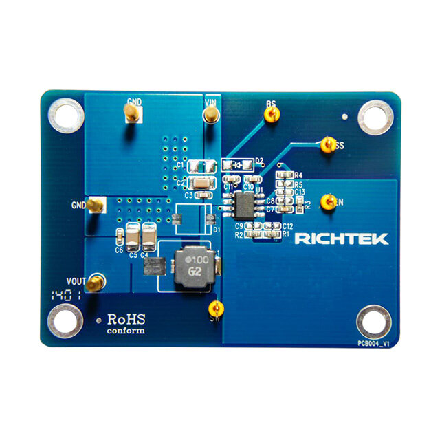
| 产品图片 |
|
| rohs | 符合RoHS含铅 / 不受限制有害物质指令(RoHS)规范要求限制 |
| 产品系列 | 电源管理IC开发工具,Texas Instruments UCC25600EVM-644- |
| 数据手册 | 点击此处下载产品Datasheethttp://www.ti.com/lit/pdf/slou293 |
| 产品型号 | UCC25600EVM-644 |
| 主要用途 | AC/DC,主面和辅面,带 PFC |
| 产品 | Evaluation Modules |
| 产品种类 | 电源管理IC开发工具 |
| 使用的IC/零件 | UCC25600 |
| 其它名称 | 296-37529 |
| 制造商产品页 | http://www.ti.com/general/docs/suppproductinfo.tsp?distId=10&orderablePartNumber=UCC25600EVM-644 |
| 功率-输出 | 600W |
| 商标 | Texas Instruments |
| 工具用于评估 | TAS5630/TA5631 |
| 所含物品 | 板 |
| 描述/功能 | Designed for audio amplifier |
| 最大工作温度 | + 50 C |
| 最小工作温度 | 0 C |
| 板类型 | 完全填充 |
| 标准包装 | 1 |
| 用于 | TAS5630/TA5631 |
| 电压-输入 | 108 ~ 265 VAC |
| 电压-输出 | 50V |
| 电流-输出 | 12A |
| 相关产品 | /product-detail/zh/UCC25600D/296-23976-5-ND/1981061/product-detail/zh/UCC25600DR/296-38315-2-ND/2048154/product-detail/zh/UCC25600DRG4/UCC25600DRG4-ND/2048155 |
| 稳压器拓扑 | 谐振 |
| 类型 | Power Management Specialized |
| 输入电压 | 390 V |
| 输出和类型 | 1,隔离 |
| 输出电压 | 12 V |
| 频率-开关 | - |


- 商务部:美国ITC正式对集成电路等产品启动337调查
- 曝三星4nm工艺存在良率问题 高通将骁龙8 Gen1或转产台积电
- 太阳诱电将投资9.5亿元在常州建新厂生产MLCC 预计2023年完工
- 英特尔发布欧洲新工厂建设计划 深化IDM 2.0 战略
- 台积电先进制程称霸业界 有大客户加持明年业绩稳了
- 达到5530亿美元!SIA预计今年全球半导体销售额将创下新高
- 英特尔拟将自动驾驶子公司Mobileye上市 估值或超500亿美元
- 三星加码芯片和SET,合并消费电子和移动部门,撤换高东真等 CEO
- 三星电子宣布重大人事变动 还合并消费电子和移动部门
- 海关总署:前11个月进口集成电路产品价值2.52万亿元 增长14.8%

PDF Datasheet 数据手册内容提取
Product Sample & Technical Tools & Support & Folder Buy Documents Software Community UCC25600 SLUS846C–SEPTEMBER2008–REVISEDJUNE2015 UCC25600 8-Pin High-Performance Resonant Mode Controller 1 Features 3 Description • VariableSwitchingFrequencyControl The UCC25600 high performance, resonant mode 1 controller is designed for dc-to-dc applications using • ProgrammableMinimumSwitchingFrequency resonant topologies, especially the LLC half-bridge With4%Accuracy(3%AccuracyatTemperature resonant converter. This highly integrated controller Range:–20°Cto105°C) implements frequency modulation control and • ProgrammableMaximumSwitchingFrequency complete system functions in only an 8-pin package. Switching to the UCC25600 will greatly simplify the • ProgrammableDeadTimeforBestEfficiency system design and layout, and improve time to • ProgrammableSoft-StartTime market, all at a price point lower than competitive 16- • EasyONandOFFControl pindeviceofferings. • OvercurrentProtection The internal oscillator supports the switching • OvertemperatureProtection frequencies from 40 kHz to 350 kHz. This high- • BiasVoltageUVLOandOvervoltageProtection accuracy oscillator realizes the minimum switching frequency limiting with 4% tolerance, allowing the • IntegratedGateDriverWith0.4-ASourceand0.8- designer to avoid over-design of the power stage ASinkCapability and, thus, further reducing overall system cost. The • OperatingTemperatureRange:–40°Cto125°C programmable dead time enables zero-voltage • SOIC8-PinPackage switching with minimum magnetizing current. This maximizes system efficiency across a variety of 2 Applications applications. The programmable soft-start timer maximizes design flexibility demanded by the varied • 100-Wto1-kWPowerSupplies requirements of end equipment using a half-bridge • LCD,Plasma,andDLP®TVs topology. By incorporating a 0.4-A source and 0.8-A sink driving capability, a low cost, reliable gate driver • Adaptors,Computing,andATXPowerSupplies transformerisarealoption. • HomeAudioSystems The UCC25600 delivers complete system protection • ElectronicLightingBallasts functions including overcurrent, UVLO, bias supply OVP,andovertemperatureprotection. DeviceInformation(1) PARTNUMBER PACKAGE BODYSIZE(NOM) UCC25600 SOIC(8) 3.91mm×4.90mm (1) For all available packages, see the orderable addendum at theendofthedatasheet. TypicalApplicationDiagram + UCC25600 8 GD1 OC 3 VS 5 GD2 RT 2 7 VCC DT 1 6 GND SS 4 1 An IMPORTANT NOTICE at the end of this data sheet addresses availability, warranty, changes, use in safety-critical applications, intellectualpropertymattersandotherimportantdisclaimers.PRODUCTIONDATA.
UCC25600 SLUS846C–SEPTEMBER2008–REVISEDJUNE2015 www.ti.com Table of Contents 1 Features.................................................................. 1 7.3 FeatureDescription.................................................10 2 Applications........................................................... 1 7.4 DeviceFunctionalModes........................................13 3 Description............................................................. 1 8 ApplicationandImplementation........................ 14 4 RevisionHistory..................................................... 2 8.1 ApplicationInformation............................................14 8.2 TypicalApplication .................................................18 5 PinConfigurationandFunctions......................... 3 9 PowerSupplyRecommendations...................... 22 6 Specifications......................................................... 4 10 Layout................................................................... 22 6.1 AbsoluteMaximumRatings......................................4 6.2 ESDRatings ............................................................4 10.1 LayoutGuidelines.................................................22 6.3 RecommendedOperatingConditions.......................4 10.2 LayoutExample....................................................23 6.4 ThermalInformation..................................................4 11 DeviceandDocumentationSupport................. 24 6.5 ElectricalCharacteristics...........................................5 11.1 CommunityResources..........................................24 6.6 TypicalCharacteristics..............................................7 11.2 Trademarks...........................................................24 7 DetailedDescription.............................................. 9 11.3 ElectrostaticDischargeCaution............................24 7.1 Overview...................................................................9 11.4 Glossary................................................................24 7.2 FunctionalBlockDiagram.........................................9 12 Mechanical,Packaging,andOrderable Information........................................................... 24 4 Revision History NOTE:Pagenumbersforpreviousrevisionsmaydifferfrompagenumbersinthecurrentversion. ChangesfromRevisionB(June2011)toRevisionC Page • AddedESDRatingstable,FeatureDescriptionsection,DeviceFunctionalModes,ApplicationandImplementation section,PowerSupplyRecommendationssection,Layoutsection,DeviceandDocumentationSupportsection,and Mechanical,Packaging,andOrderableInformationsection. ................................................................................................ 1 ChangesfromRevisionA(September2008)toRevisionB Page • ChangedOperatingTemperatureRangetomatchtheElectricalSpecifications................................................................... 1 2 SubmitDocumentationFeedback Copyright©2008–2015,TexasInstrumentsIncorporated ProductFolderLinks:UCC25600
UCC25600 www.ti.com SLUS846C–SEPTEMBER2008–REVISEDJUNE2015 5 Pin Configuration and Functions DPackage 8-PinSOIC TopView DT 1 8 GD1 RT 2 7 VCC OC 3 6 GND SS 4 5 GD2 Table1.PinFunctions PIN I/O DESCRIPTION NAME NO. Thispinsetsthedeadtimeofhigh-sideandlow-sideswitchdrivingsignals.Connectaresistorto ground.Withinternal2.25-Vvoltagereference,thecurrentflowingthroughtheresistorsetsthe DT 1 I deadtime.Topreventshootthroughwhenthispinisaccidentallyshortedtoground,the minimumdeadtimeissetto120ns.Anydeadtimesettinglessthan120nswillautomatically have120-nsdeadtime. GD1 8 High-sideandlow-sideswitchgatedriver.Connectgatedrivertransformerprimarysidetothese O GD2 5 twopinstodrivethehalf-bridge. GND 6 – Ground Overcurrentprotectionpin.Whenthevoltageonthispinisabove1V,gatedriversignalsare activelypulledlow.Afterthevoltagefallsbelow0.6V,thegatedriversignalrecoverswithsoft- OC 3 I start.WhenOCpinvoltageisabove2V,thedeviceislatchedoff.BringingVCCbelowthe UVLOlevelresetstheovercurrentlatchtooff. Thecurrentflowingoutofthispinsetsthefrequencyofthegatedriversignals.Connecttheopto- couplercollectortothispintocontroltheswitchingfrequencyforregulationpurposes.Parallela resistortogroundtosettheminimumcurrentflowingoutofthepinandsettheminimum RT 2 I switchingfrequency.Tosetthemaximumswitchingfrequencylimiting,simplyseriesaresistor withtheopto-couplertransistor.Thisresistorsetsthemaximumcurrentflowingoutofthepinand limitsthemaximumswitchingfrequency. Soft-startpin.Thispinsetsthesoft-starttimeofthesystem.Connectacapacitortoground. Pullingthispinbelow1VwilldisablethedevicetoalloweasyON/OFFcontrol.Thesoft-start SS 4 I functionisenabledafterallfaultconditions,includingbiassupplyOV,UVLO,overcurrent protection,andovertemperatureprotection. BiasSupply.Connectthispintoapowersupplylessthan20V.Parallela1-μFcapacitorto VCC 7 – groundtofilteroutnoise. Copyright©2008–2015,TexasInstrumentsIncorporated SubmitDocumentationFeedback 3 ProductFolderLinks:UCC25600
UCC25600 SLUS846C–SEPTEMBER2008–REVISEDJUNE2015 www.ti.com 6 Specifications 6.1 Absolute Maximum Ratings overoperatingfree-airtemperaturerange(unlessotherwisenoted) (1) MIN MAX UNIT Supplyvoltage,VCC 22 V Voltage,GD1,GD2 –0.5 VCC+0.5 V Gatedrivecurrent–continuous,GD1,GD2 ±25 mA Current,RT –5 mA Current,DT –0.7 mA Leadtemperature(10seconds) 260 °C Operatingjunctiontemperature,T –40 125 °C J Storagetemperature,T –65 150 °C stg (1) StressesbeyondthoselistedunderAbsoluteMaximumRatingsmaycausepermanentdamagetothedevice.Thesearestressratings only,whichdonotimplyfunctionaloperationofthedeviceattheseoranyotherconditionsbeyondthoseindicatedunderRecommended OperatingConditions.Exposuretoabsolute-maximum-ratedconditionsforextendedperiodsmayaffectdevicereliability. 6.2 ESD Ratings VALUE UNIT Humanbodymodel(HBM),perANSI/ESDA/JEDECJS-001,allpins(1) ±2000 V(ESD) Electrostaticdischarge Chargeddevicemodel(CDM),perJEDECspecificationJESD22-C101,all V pins(2) ±500 (1) JEDECdocumentJEP155statesthat500-VHBMallowssafemanufacturingwithastandardESDcontrolprocess. (2) JEDECdocumentJEP157statesthat250-VCDMallowssafemanufacturingwithastandardESDcontrolprocess. 6.3 Recommended Operating Conditions overoperatingfree-airtemperaturerange(unlessotherwisenoted) MIN NOM MAX UNIT VCCinputvoltagefromalow-impedancesource 11.5 18.0 V RTresistance 1 8.666 kΩ DTresistance 3.3 39 kΩ SScapacitor 0.01 1 μF 6.4 Thermal Information UCC25600 THERMALMETRIC(1) D(SOIC) UNIT 8PINS R Junction-to-ambientthermalresistance 118.5 °C/W θJA R Junction-to-case(top)thermalresistance 72.5 °C/W θJC(top) R Junction-to-boardthermalresistance 58.9 °C/W θJB ψ Junction-to-topcharacterizationparameter 24.1 °C/W JT ψ Junction-to-boardcharacterizationparameter 58.4 °C/W JB (1) Formoreinformationabouttraditionalandnewthermalmetrics,seetheSemiconductorandICPackageThermalMetricsapplication report,SPRA953. 4 SubmitDocumentationFeedback Copyright©2008–2015,TexasInstrumentsIncorporated ProductFolderLinks:UCC25600
UCC25600 www.ti.com SLUS846C–SEPTEMBER2008–REVISEDJUNE2015 6.5 Electrical Characteristics overoperatingfree-airtemperaturerange(unlessotherwisenoted) PARAMETER TESTCONDITIONS MIN TYP MAX UNIT BIASSUPPLY(VCC) VCCcurrent,disabled SS=0V 1 1.5 mA VCCcurrent,enabled SS=5V,C =C =1nF 2.5 5 7.5 GD1 GD2 VCCcurrent,UVLO VCC=9V 100 400 μA UVLOturn-onthreshold MeasuredatVCCrising 9.9 10.5 11.1 V UVLOturn-offthreshold MeasuredatVCCfalling 8.9 9.5 10.1 UVLO UVLOhysteresis MeasuredatVCC 0.7 1 1.3 V OVPturn-offthreshold MeasuredatVCCrising 18 20 22 V OVPturn-onthreshold MeasuredatVCCfalling 16 18 20 OVP OVPhysteresis MeasuredatVCC 1.5 2 2.5 DEADTIME(DT) T Deadtime R =16.9kΩ 390 420 450 ns DT DT OSCILLATOR Minimumswitchingfrequencyat –40°Cto125°C 40.04 41.70 43.36 F kHz SW(min) GD1,GD2 –20°Cto105°C 40.45 41.70 42.95 K Switchingfrequencygain/I(RT) R =4.7kΩ,I =0to1mA 60 80 100 Hz/μA ICO RT RT GD1,GD2ontimemismatching –50 50 ns Switchingfrequencystartingburst SS=5V 300 350 400 mode F SW_BM Switchingfrequencytocomeoutof burstmode SS=5V 280 330 380 kHz –40°Cto125°C 122 142.5 162 F Switchingfrequencyatsoft-start SW(start) –20°Cto105°C 125 142.5 160 EXTERNALDISABLE/SOFTSTART Enablethreshold MeasureatSSrising 1.1 1.2 1.3 Disablethreshold MeasuredatSSfalling 0.85 1 1.1 V Disablehysteresis MeasuredatSS 0.15 0.35 MeasuredbetweenSS(falling)and Disableprop.delay 250 500 750 ns GD2(falling) SourcecurrentonISSpin V =0.5V –225 –175 –125 SS I μA SS SourcecurrentonISSpin V =1.35V –5.5 –5 –4.5 SS PEAKCURRENTLIMIT Level1overcurrentthreshold–V V OC 0.9 1 1.1 OC1(off) rising Level2overcurrentlatchthreshold– V 1.8 2.0 2.2 V OC2(off) V rising OC Level1overcurrentthreshold–V V OC 0.5 0.6 0.7 OC1(on) falling T Propagationdelay 60 200 500 ns d_OC I OCbiascurrent V =0.8V –200 200 nA OC OC Copyright©2008–2015,TexasInstrumentsIncorporated SubmitDocumentationFeedback 5 ProductFolderLinks:UCC25600
UCC25600 SLUS846C–SEPTEMBER2008–REVISEDJUNE2015 www.ti.com Electrical Characteristics (continued) overoperatingfree-airtemperaturerange(unlessotherwisenoted) PARAMETER TESTCONDITIONS MIN TYP MAX UNIT GATEDRIVE GD1,GD2outputvoltagehigh I ,I =−20mA 9 11 V GD1 GD2 GD1,GD2onresistancehigh I ,I =−20mA 12 30 Ω GD1 GD2 GD1,GD2outputvoltagelow I ,I =20mA 0.08 0.2 V GD1 GD2 GD1,GD2onresistancelow I ,I =20mA 4 10 Ω GD1 GD2 RisetimeGDx 1Vto9V,C =1nF 18 35 LOAD ns FalltimeGDx 9Vto1V,C =1nF 12 25 LOAD GD1,GD2outputvoltageduring VCC=6V,I ,I =1.2mA 0.5 1.75 V UVLO GD1 GD2 THERMALSHUTDOWN Thermalshutdownthreshold 160 Thermalshutdownrecovery °C 140 threshold 6 SubmitDocumentationFeedback Copyright©2008–2015,TexasInstrumentsIncorporated ProductFolderLinks:UCC25600
UCC25600 www.ti.com SLUS846C–SEPTEMBER2008–REVISEDJUNE2015 6.6 Typical Characteristics AtV =12V,R =4.7kΩ,R =16.9kΩ,V =5V,V =0V;allvoltagesarewithrespecttoGND,T =T =25°C, CC RT DT SS OC J A unlessotherwisenoted. 1 350 A 0.9 m Hz 300 plyCurrent- 000...678 Frequency-k 220500 up 0.5 ng S hi Bias 0.4 Switc 150 - 0.3 - c w 100 Ivc 0.2 OCOpen Fs -40°C 50 25°C 0.1 125°C 0 0 6 7 8 9 10 11 12 13 14 0 1 2 3 4 5 Vvcc-BiasSupplyVoltage-V IRT-RTCurrent-mA Figure1.BiasSupplyCurrentvsBiasSupplyVoltage Figure2.SwitchingFrequencyvsRTCurrent 1000 1000 900 -40°C 900 25°C 800 125°C 800 - 700 - 700 e e m m Ti 600 Ti 600 d d Dea 500 Dea 500 - - DT 400 DT 400 300 300 200 200 -40°C 100 100 25°C 125°C 0 0 0 100 200 300 400 500 600 700 0 5 10 15 20 25 30 35 40 45 IDT-DTCurrent-uA RDT-DTResistor-kOhm Figure3.DeadTimevsDTCurrent Figure4.DeadTimevsDTResistor 16 1.6 16 0.8 GateDrive 14 Voltage 1.4 14 0.7 GateDriveSink 12 Current 1.2 12 0.6 V A V A Voltage-108 01.8 Current- Voltage-108 GGaatteeDDrriivveeVSoolutarcgee 00..45 Current- Drive 6 0.6 Drive Drive 6 Current 0.3 Drive Gate 4 0.4 Gate Gate 4 0.2 Gate 2 0.2 2 0.1 0 0 0 0 -2 -0.2 -2 -0.1 0 100 200 300 400 500 600 0 200 400 600 800 1000 Time-ns Time-ns Figure5.GateDriveFalling,VCC=15V Figure6.GateDriveRising,VCC=15V Copyright©2008–2015,TexasInstrumentsIncorporated SubmitDocumentationFeedback 7 ProductFolderLinks:UCC25600
UCC25600 SLUS846C–SEPTEMBER2008–REVISEDJUNE2015 www.ti.com Typical Characteristics (continued) AtV =12V,R =4.7kΩ,R =16.9kΩ,V =5V,V =0V;allvoltagesarewithrespecttoGND,T =T =25°C, CC RT DT SS OC J A unlessotherwisenoted. 300 12 UVLOOnThreshold-VCCRising 250 UVLOOffThreshold-VCCFalling ationDelay-ns 125000 OThreshold- 1101 opag UVL Pr 100 9 50 0 8 -60 -40 -20 0 20 40 60 80 100 120 140 -60 -40 -20 0 20 40 60 80 100 120 140 Tj-JunctionTemperature-°C Tj-JunctionTemperature- °C Figure7.OvercurrentPropagationDelayvsTemperature Figure8.UVLOThresholdvsTemperature 22 2.5 d-V 21 OOVVPPOOfnfTThhrreesshhoolldd--VVCCCCFRailsliinngg d-V 2 Threshol 20 Threshol 1.5 OOCCOOfnfTThhrreesshhoolldd--VVooccRFaislilningg oltage 19 urrent OCLatchThreshold-VocRising V C Over 18 Over 1 VCC Voc 0.5 17 16 0 -60 -40 -20 0 20 40 60 80 100 120 140 -60 -40 -20 0 20 40 60 80 100 120 140 Tj-JunctionTemperature- °C Tj-JunctionTemperature- °C Figure9.VCCOvervoltageThresholdvsTemperature Figure10.OvercurrentThresholdvsTemperature 100 80 s n - h matc 60 s Mi e m Ti 40 n O 20 0 0 50 100 150 200 250 300 350 SwitchingFrequency-kHz Figure11.On-timeMismatchvsSwitchingFrequency 8 SubmitDocumentationFeedback Copyright©2008–2015,TexasInstrumentsIncorporated ProductFolderLinks:UCC25600
UCC25600 www.ti.com SLUS846C–SEPTEMBER2008–REVISEDJUNE2015 7 Detailed Description 7.1 Overview Duetohighpowerdensityandhighefficiencyrequirements,LLCtopologyisemployedinmanyapplications.The LLC resonant converter has many unique characteristics and improvements compared with hard-switch bridge topology and phase-shift full bridge. For example, LLC has a simple structure, and could achieve primary MOSFET zero voltage switching (ZVS) and the secondary rectifier zero current switching (ZCS) from no load to fullload. The UCC25600 device is an LLC-resonant half-bridge controller which integrates built-in, state-of-the-art efficiencyboostfeatureswithhigh-levelprotectionfeaturestoprovidecost-effectivesolutions. 7.2 Functional Block Diagram 2.25V T + J TSD 20V 160oC/140oC 18V OV DT Thermal 1 ShutDown + R Deadtime 10.5V + UVLO DT 9.5V generator 2.5V 7 VCC Feed RT 2 back Ic OSC 8 GD1 Vss UVLO Q SET D VCC OV OC FAULT 5 GD2 TSD Q CLR 6V GD_Stop 6 GND 5uA 170uA OC OC + 3 Vss 1V SS 4 OC_latch + Css + 2V 1.2V/1V FAULT SSETQ RCLRQ Copyright©2008–2015,TexasInstrumentsIncorporated SubmitDocumentationFeedback 9 ProductFolderLinks:UCC25600
UCC25600 SLUS846C–SEPTEMBER2008–REVISEDJUNE2015 www.ti.com 7.3 Feature Description 7.3.1 SoftStart During start-up and fault recovery conditions, soft start is always implemented to prevent excessive resonant tank current and to ensure zero-voltage switching (ZVS). During soft start, the switching frequency is increased. Thesoft-starttimecanbeprogrammedbyplacingacapacitorfromtheSSpintoground. The soft-start pin also serves as an ON/OFF control pin of the device. By actively pulling the SS pin below 1 V, the device is disabled. When the pulldown is removed, SS pin voltage is increased because of internal charging current. Once the SS pin is above 1.2 V, the device starts to generate a gate-driver signal and enters soft-start mode.ThetimesequenceofsoftstartisshowninFigure12. 4V 1.2V Vss Gatedriver t t ss_delay ss Figure12. Soft-StartSequence To prevent a long delay between the ON command and appearance of a gate driver signal, the SS pin current is setastwodifferentlevels.WhentheSSpinvoltageisbelow1.2V,itsoutputcurrentis175 μA.Thishighcurrent could charge the soft-start pin capacitor to 1.2 V in a short period of time, and reduce the time delay. This time delaycanbecalculatedusingfollowingequation: 1.2V t = C SS_delay 175mA SS (1) 10 SubmitDocumentationFeedback Copyright©2008–2015,TexasInstrumentsIncorporated ProductFolderLinks:UCC25600
UCC25600 www.ti.com SLUS846C–SEPTEMBER2008–REVISEDJUNE2015 Feature Description (continued) The switching frequency during soft start is determined by both the current flowing out of the RT pin and the voltageontheSSpin.Theswitchingfrequencycanbecalculatedbasedonthefollowingequation: 1 1 f = S 2 6ns´1A +150ns æ V ö I +ç1.81mA- SS ÷ RT è 2.2kWø (2) After the SS pin voltage reaches 4 V, the soft-start period is finished and switching frequency becomes the same asdemandedbytheRTpincurrent.ThetimeusedtochargetheSSpinfrom1.2Vto4Visdefinedassoft-start timeandcanbecalculatedas: 2.8V t = C SS 5mA SS (3) To ensure reliable operation, the gate drivers restart with GD2 turning high. This prevents uncertainty during systemstartup. 7.3.2 OvercurrentProtection To prevent power stage failure under excessive load current condition, the UCC25600 includes an overcurrent protection function. With a dedicated OC pin, the power stage is shut down when OC pin voltage is above 1 V. Once the OC pin voltage becomes lower than 0.6 V, the gate driver recovers with a soft start. To enhance system safety, the UCC25600 latches up the whole system when the OC pin becomes above 2 V. Bring VCC belowtheUVLOleveltoresetthedevice. The current can be indirectly sensed through the voltage across the resonant capacitor by using the sensing networkshowninFigure13. L r Fromhalfbridge TR L m C ToOC D2 Rs s Cp Rp D1 Cr Figure13. CurrentSensingforLLCResonantConverter Thegeneralconceptofthissensingmethodisthattheacvoltageacrosstheresonantcapacitorisproportionalto loadcurrent. AccordingtotheFHAmodel,peakvoltageoftheaccomponentontheresonantcapacitorcanbecalculatedas: 4 jf L Q +1 V = nV n n e Cr_pk p o f 2L n n (4) Therefore, the resonant capacitor voltage reaches its maximum value at the minimum switching frequency and maximum load. According to this equation, the current sensing network components can be calculated. Due to thenatureofFHA,thefinalcircuitparametersneedtobeverifiedthroughactualhardwaretest. Copyright©2008–2015,TexasInstrumentsIncorporated SubmitDocumentationFeedback 11 ProductFolderLinks:UCC25600
UCC25600 SLUS846C–SEPTEMBER2008–REVISEDJUNE2015 www.ti.com Feature Description (continued) Table2.CalculatedCurrentSensingNetworkComponents NAME FUNCTION DESIGNEQUATION V (max)2 R Transferacvoltageacrossresonant R = Cr_pk S capacitorintocurrentsource s 2P (max) Rs (5) 10 C = C Blockingdcvoltageonresonantcapacitor S s R f s min (6) R R = s p R Loadresistorofthecurrentsource P p V (max) Cr_pk (7) 10 C = CP Filtercapacitor p R f p min (8) 7.3.3 GateDriver The half-bridge resonant converter is controlled by the nearly 50% duty-cycle variable frequency square-wave voltage. This allows the half bridge to be easily driven by the gate-driver transformer. Compared with a half- bridgedriverdevice,agate-drivertransformerprovidesasimpleandreliablesolution,which: • Eliminatestheneedforgatedriverpowersupply • Enablessimplifiedlayout • Preventsshoot-throughduetothetransformercoupling • Requiresnolatchup The UCC25600 integrates two-gate drivers with 0.4-A source and 0.8-A sink capability to directly drive the gate- drivertransformer. For the LLC resonant converter, it is critical for the gate-driver signal to be precisely symmetrical. Otherwise, the resonant tank operation will be symmetrical. The load current distribution will be unbalanced for the output rectifiers,whichinturnrequiretheover-designofthepowerstagesandthermalmanagement. In UCC25600, the gate-driver output is precisely trimmed to have less than 50-ns mismatch. Although the gate- driver signal is quite symmetrical, it is still recommended to insert the dc blocking capacitor in the gate-driver transformerprimarysidetopreventtransformersaturationduringfasttransients. 7.3.4 OvertemperatureProtection UCC25600 continuously senses its junction temperature. When its junction temperature rises above 160°C, the device will enter overtemperature protection mode with both gate drivers actively pulled low. When junction temperaturedropsbelow140°C,gatedriverrestartswithsoftstart. 12 SubmitDocumentationFeedback Copyright©2008–2015,TexasInstrumentsIncorporated ProductFolderLinks:UCC25600
UCC25600 www.ti.com SLUS846C–SEPTEMBER2008–REVISEDJUNE2015 7.4 Device Functional Modes 7.4.1 Burst-ModeOperation During light load condition, the resonant converter tends to increase its switching frequency and maintain the output voltage regulation. However, due to ringing caused by the transformer parasitic capacitor and the rectification-diode-junction capacitors, the energy could be directly transferred to the load through these capacitors. When this power becomes more than the load requires, the output voltage become higher than the regulationlevel.Inthiscase,furtherincreasingtheswitchingfrequencywillnothelpthesituationbecauseenergy transfertotheloadisnotthroughthepowerstageitself. To prevent output overvoltage during this condition, the UCC25600 includes the burst-mode operation function. When the control loop demands switching frequency higher than 350 kHz, the gate driver is disabled and the power stage stops switching. When the output voltage drops, the control loop begins to demand switching frequency less than 330 kHz, the gate driver recovers and the power stage begins to deliver power again. This allowstheoutputvoltagetoberegulated. Thisburstmodecanbeeasilydisabledbylimitingthemaximumswitchingfrequencytolessthan350kHz.Inthis way,thecontrolloopwillneverdemandaswitchingfrequencyhigherthan350kHzandburstmodeoperationwill notoccur. 7.4.2 VCC When VCC becomes above 10.5 V, the device is enabled and, after all fault conditions are cleared, the gate driver starts with soft start. When VCC drops below 9.5 V, the device enters the UVLO protection mode and both gate drivers are actively pulled low. When VCC rises above 20 V, the device enters VCC overvoltage protection mode and the device is disabled with both gate drivers actively pulled low. The VCC overvoltage protection will recoverwithsoftstartwhentheVCCvoltagereturnsbelow18V. Copyright©2008–2015,TexasInstrumentsIncorporated SubmitDocumentationFeedback 13 ProductFolderLinks:UCC25600
UCC25600 SLUS846C–SEPTEMBER2008–REVISEDJUNE2015 www.ti.com 8 Application and Implementation NOTE Information in the following applications sections is not part of the TI component specification, and TI does not warrant its accuracy or completeness. TI’s customers are responsible for determining suitability of components for their purposes. Customers should validateandtesttheirdesignimplementationtoconfirmsystemfunctionality. 8.1 Application Information The UCC25600 device is a high performance, resonant-mode controller designed for DC/DC applications using resonanttopologies,especiallytheLLChalf-bridgeresonantconverter. 8.1.1 PrincipalofOperation The soft-switching capability, high efficiency, and long holdup time make the LLC resonant converter attractive for many applications, such as digital TV, ac-to-dc adapters, and computer power supplies. Figure 14 shows the schematicoftheLLCresonantconverter. Cr Lr n:1:1 Lm Figure14. LLCResonantConverter The LLC resonant converter is based on the series resonant converter (SRC). By using the transformer magnetizing inductor, zero-voltage switching can be achieved over a wide range of input voltage and load. As a result of multiple resonances, zero-voltage switching can be maintained even when the switching frequency is higher or lower than resonant frequency. This simplifies the converter design to avoid the zero-current switching region which can lead to system damage. The converter achieves the best efficiency when operated close to its resonant frequency at a nominal input voltage. As the switching frequency is lowered, the voltage gain is significantly increased. This allows the converter to maintain regulation when the input voltage falls low. These features make the converter ideally suited to operate from the output of a high-voltage, boost PFC pre-regulator, allowingittoholdupthroughbriefperiodsofacline-voltagedropout. Due to the nature of resonant converter, all the voltages and currents on the resonant components are approximately sinusoidal. The gain characteristic of the LLC resonant converter is analyzed based on the first harmonic approximation (FHA), which means all the voltages and currents are treated as a sinusoidal shape with thefrequencythesameastheswitchingfrequency. According to the operation principle of the converter, the LLC resonant converter can be drawn as the equivalent circuitshowninFigure15. Cr Lr Vge Lm Re Voe Figure15. LLCResonantConverterEquivalentCircuit 14 SubmitDocumentationFeedback Copyright©2008–2015,TexasInstrumentsIncorporated ProductFolderLinks:UCC25600
UCC25600 www.ti.com SLUS846C–SEPTEMBER2008–REVISEDJUNE2015 Application Information (continued) In this equivalent circuit, the V and V are the fundamental harmonics of the voltage generated by the half- ge oe bridge and the voltage on the transformer primary side, respectively. These voltages can be calculated through Fourieranalysis.TheloadresistorR istheequivalentresistoroftheload,anditcanbecalculatedas: e 8 R = n2R e p2 (9) Basedonthisequivalentcircuit,theconvertergainatdifferentswitchingfrequenciescanbecalculatedas: jwL R m e V jwL +R o = m e V / 2 jwL R 1 DC m e + + jwL jwL +R jwC r m e r (10) InthisequationV /2istheequivalentinputvoltageduetothehalf-bridgestructure. DC Table3.CircuitDefinitionCalculations RESONANT NORMALIZED NORMALIZEDGAIN QUALITYFACTOR INDUCTORRATIO FREQUENCY FREQUENCY V 1 M =VDCo/ 2 f0 = 2p LrCr Qe = LrR/eCr fn = ff0 (14) Ln = LLmr (15) (11) (12) (13) FollowingthedefinitionsinTable3,theconvertergainatdifferentswitchingfrequenciescanbewrittenas: L ´f2 M= n n é(L +1)´f2 -1ù+jé(f2 -1)´f ´Q ´L ù ë n n û ë n n e nû (16) BecauseoftheFHA,thisgainequationisanapproximation.Whentheswitchingfrequencymovesawayfromthe resonant frequency, the error becomes larger. However, this equation can be used as a design tool. The final resultsneedtobeverifiedbythetime-basedsimulationorhardwaretest. Copyright©2008–2015,TexasInstrumentsIncorporated SubmitDocumentationFeedback 15 ProductFolderLinks:UCC25600
UCC25600 SLUS846C–SEPTEMBER2008–REVISEDJUNE2015 www.ti.com From Equation 16, when the switching frequency is equal to the resonant frequency, f = 1 and converter voltage n gain is equal to 1. Converter gain at different loads and inductor ratio conditions are shown in Figure 16 through Figure19. 2 2 Q =0.1 Q =0.1 Qe=0.2 Qe=0.2 Qe=0.5 Qe=0.5 Qe=1 Qe=1 1.5 Qe=2 1.5 Qe=2 Qe=5 Qe=5 e e M M 1 1 0.5 0.5 0 0 0.1 0.5 1 1.5 2 0.1 0.5 1 1.5 2 f f n n Figure16.Mvsf Figure17.Mvsf N N 2 2 Q =0.1 Q =0.1 Qe=0.2 Qe=0.2 Qe=0.5 Qe=0.5 Qe=1 Qe=1 1.5 Qe=2 1.5 Qe=2 Qe=5 Qe=5 e e M M 1 1 0.5 0.5 0 0 0.1 0.5 1 1.5 2 0.1 0.5 1 1.5 2 f f n n Figure18.Mvsf Figure19.Mvsf N N Based on its theory of operation, the LLC resonant converter is controlled through pulse frequency modulation (PFM). The output voltage is regulated by adjusting the switching frequency according to the input and output conditions. Optimal efficiency is achieved at the nominal input voltage by setting the switching frequency close to the resonant frequency. When the input voltage drops low, the switching frequency is decreased to boost the gainandmaintainregulation. The UCC25600 resonant half-bridge controller uses variable switching frequency control to adjust the resonant tank impedance and regulate output voltage. This 8-pin package device integrates the critical functions for optimizingthesystemperformancewhilegreatlysimplifyingthedesignandlayout. 16 SubmitDocumentationFeedback Copyright©2008–2015,TexasInstrumentsIncorporated ProductFolderLinks:UCC25600
UCC25600 www.ti.com SLUS846C–SEPTEMBER2008–REVISEDJUNE2015 8.1.2 AdjustableDeadTime Resonant half-bridge converter relies on the resonant tank current at MOSFETs turn-off to achieve soft switching andreduceswitchingloss.Higherturn-offcurrentprovidesmoreenergytodischargethejunctioncapacitor,while it generates more turn-off loss. Smaller turn-off current reduces turn-off loss, but it requires longer time to discharge MOSFETs junction capacitors and achieve soft switching. By choosing an appropriate dead time, turn- offcurrentisminimizedwhilestillmaintainingzero-voltageswitching,andbestsystemperformanceisrealized. In UCC25600, dead time can be adjusted through a single resistor from the DT pin to ground. With internal 2.25- Vvoltagereference,thecurrentflowthroughtheresistorsetsthedeadtime. t =20ns+R ´24ns/ kW d dt (17) To prevent shoot through when the DT pin accidentally connects to ground, a minimum 120-ns dead time is insertedintothe2gatedriveroutputs.Anydead-timesettinglessthan120nswillbelimitedto120ns. 8.1.3 Oscillator With variable switching frequency control, UCC25600 relies on the internal oscillator to vary the switching frequency. The oscillator is controlled by the current flowing out of the RT pin. Except during soft start, the relationshipbetweenthegatesignalfrequencyandthecurrentflowingoutoftheRTpincanberepresentedas: 1 1 f = » I ´83Hz/ mA S 2 6ns´1A RT +150ns I RT (18) Because the switching frequency is proportional to the current, by limiting the maximum and minimum current flowing out of the RT pin, the minimum and maximum switching frequency of the converter could be easily limited. As shown in Figure 20, putting a resistor from the RT pin to ground limits the minimum current and puttingaresistorinserieswiththeopto-couplerlimitsthemaximumcurrent. UCC25600 Maximum frequencylimiting RT R1 Minimum R2 frequencylimiting Figure20. MaximumandMinimumFrequencySettingforUCC25600 Copyright©2008–2015,TexasInstrumentsIncorporated SubmitDocumentationFeedback 17 ProductFolderLinks:UCC25600
UCC25600 SLUS846C–SEPTEMBER2008–REVISEDJUNE2015 www.ti.com Thefrequencylimitingresistorcanbecalculatedbasedonfollowingequations. 6ns I = fmax 1 -150ns 2f max (19) 6ns I = fmin 1 -150ns 2f min (20) æ 1 1 ö I = 2.5V ç + ÷ fmax è R R ø 1 2 (21) 2.5V I = fmin R 2 (22) 8.2 Typical Application This design example describes the HPA341 EVM design and outlines the design steps required to design a 300- W LLC resonant half-bridge converter, which provides a regulated output voltage nominally at 12 V at maximum 300 W of load power, with reinforced isolation of AC-DC off-line applications between the primary and the secondary,operatingfromaDCsourceof390V. +375to405Vdc 12V@25A + + + 11V + 12VBias (External) + + + Figure21. TypicalApplicationSchematic 18 SubmitDocumentationFeedback Copyright©2008–2015,TexasInstrumentsIncorporated ProductFolderLinks:UCC25600
UCC25600 www.ti.com SLUS846C–SEPTEMBER2008–REVISEDJUNE2015 Typical Application (continued) 8.2.1 DesignRequirements Table4.DesignRequirements DESIGNPARAMETER TARGETVALUE Outputvoltage 12V Ratedoutputpower 300W InputDCvoltagerange 375Vto405V Typicalefficiencyatfullload 91% Switchingfrequency 85kHzto350kHz Resonantfrequency 130kHz 8.2.2 DetailedDesignProcedure 1. Resonantinductor(Lr),resonantcapacitor(Cr),and(Lm)ofhalf-bridgeLLC (a) TurnsratioofMaintransformer: n=Np/Ns=16.5 (23) (b) Maximumresonantgainrequired: M_max=110%×n×(2×Vout)/(Vin_min)=110%×16.5×(2×12V)/375V=1.17 (24) (c) Choose Ln and Q. The Ln range is typically selected from 3 to 9. Choose Q based on the curves below, where the peak gain must be higher than or equal to the maximum resonant gain required. Based on the belowcurves,Qselects0.45. Ln=Lm/Lr=5 (25) Q= (Lr/Cr)/Req=0.45 (26) Figure22. PeakGainvsQ (d) Calculateequivalentprimaryresistance: Req=(8×n2×Vout2)/(π2×Pout)=(8×4.62×122)/(π2×300)=108.6Ω (27) (e) SelectCr: Cr=24nF (28) (f) CalculateLr: Copyright©2008–2015,TexasInstrumentsIncorporated SubmitDocumentationFeedback 19 ProductFolderLinks:UCC25600
UCC25600 SLUS846C–SEPTEMBER2008–REVISEDJUNE2015 www.ti.com 1 fr = 2p´ Lr´Cr (29) (g) Combinetheabovetwoequations: Lr=55µH (30) (h) CalculateLm: Lm=Ln×Lr=275µH (31) 2. Calculate Rdt. In the UCC25600, dead time can be adjusted through a single resistor from DT pin to ground. Withaninternal2.25-Vvoltagereference,thecurrentflowthroughtheresistorsetsthedeadtime. td=20ns+Rdt×24ns/kΩ where • td=300ns • Rdt=11.7kΩ (32) 3. CalculateC .RefertoSoftStartformoredetails. SS tss=25ms (33) tss=2.8V/5µA×Css (34) Css=44.6nF (35) 4. A 47nF capacitor is selected. Calculate RT1 and RT2. Refer to Oscillator for more details. RT1 and RT2 are used to limit maximum switching frequency and minimum switching frequency. RT1 and RT2 can be calculatedbasedonfollowingequations: Ifmax=6ns/(1/2fmax-150ns) (36) Ifmin=6ns/(1/2fmin-150ns) (37) Ifmax=2.5V(1/RT1+1/RT2) (38) Ifmin=2.5V/RT2 (39) 5. Combinethefourequationsabove: RT1=511Ω (40) RT2=2.37kΩ (41) 6. CalculateRs,Cs,Rp,andCp.RefertoOvercurrentProtection formoredetails. Rs=300kΩ (42) Cs=22pF (43) Rp=4.99kΩ (44) Cp=1µF (45) 20 SubmitDocumentationFeedback Copyright©2008–2015,TexasInstrumentsIncorporated ProductFolderLinks:UCC25600
UCC25600 www.ti.com SLUS846C–SEPTEMBER2008–REVISEDJUNE2015 8.2.3 ApplicationCurves 60 180 45 135 (dB) 1350 4950 (Deg) ain 0 0 ase G -15 -45 h P -30 -90 -45 -135 Gain Phase -60 -180 10 100 1000 10000 100000 1000000 Frequency(Hz) Figure23.TypicalOutputVoltageTurnOn(TP15) Figure24.FullSystemLoopCompensation(TP19and TP21) Figure25.TypicalSoft-StartWaveform Figure26.TypicalResonantTankCurrentandResonant CapacitorVoltage Copyright©2008–2015,TexasInstrumentsIncorporated SubmitDocumentationFeedback 21 ProductFolderLinks:UCC25600
UCC25600 SLUS846C–SEPTEMBER2008–REVISEDJUNE2015 www.ti.com 9 Power Supply Recommendations The VCC power terminal for the device requires the direct placement of low-ESR noise-decoupling capacitance from the VCC terminal to the GND terminal. Ceramic capacitors with stable dielectric characteristics over temperature are recommended, such as X7R or better. Depending on the operating temperature range of the application, X5R may be acceptable, but the drop in capacitance value at high temperature and with applied DC- biasmaynotbetolerable.Avoiddielectricswithpoortemperaturestability. The recommended decoupling capacitor is a 1-µF 0805-sized 50-V X7R capacitor, ideally with (but not essential) a second, smaller, parallel 100-nF 0603-sized 50-V X7R capacitor. Higher voltage-rated parts can also be used. Theuseof25-Vratedpartsisnotrecommended,duetoreductionineffectivecapacitancevaluewithappliedDC bias. 10 Layout 10.1 Layout Guidelines Four-layerlayoutisrecommended A 1-µF ceramic decoupling capacitor is recommended, to be placed as close as possible between the VCC terminalandGND,andtrackeddirectlytobothterminals. PlaceC ,RDT,Rp,Cp,RT1,andRT2ascloseaspossibletotheUCC25600. SS ConnectaregulatedbiassupplytotheVCCpin. 22 SubmitDocumentationFeedback Copyright©2008–2015,TexasInstrumentsIncorporated ProductFolderLinks:UCC25600
UCC25600 www.ti.com SLUS846C–SEPTEMBER2008–REVISEDJUNE2015 10.2 Layout Example Figure27. BoardLayoutExample Copyright©2008–2015,TexasInstrumentsIncorporated SubmitDocumentationFeedback 23 ProductFolderLinks:UCC25600
UCC25600 SLUS846C–SEPTEMBER2008–REVISEDJUNE2015 www.ti.com 11 Device and Documentation Support 11.1 Community Resources The following links connect to TI community resources. Linked contents are provided "AS IS" by the respective contributors. They do not constitute TI specifications and do not necessarily reflect TI's views; see TI's Terms of Use. TIE2E™OnlineCommunity TI'sEngineer-to-Engineer(E2E)Community.Createdtofostercollaboration amongengineers.Ate2e.ti.com,youcanaskquestions,shareknowledge,exploreideasandhelp solveproblemswithfellowengineers. DesignSupport TI'sDesignSupport QuicklyfindhelpfulE2Eforumsalongwithdesignsupporttoolsand contactinformationfortechnicalsupport. 11.2 Trademarks E2EisatrademarkofTexasInstruments. isaregisteredtrademarkof~TexasIinstruments. Allothertrademarksarethepropertyoftheirrespectiveowners. 11.3 Electrostatic Discharge Caution Thesedeviceshavelimitedbuilt-inESDprotection.Theleadsshouldbeshortedtogetherorthedeviceplacedinconductivefoam duringstorageorhandlingtopreventelectrostaticdamagetotheMOSgates. 11.4 Glossary SLYZ022—TIGlossary. Thisglossarylistsandexplainsterms,acronyms,anddefinitions. 12 Mechanical, Packaging, and Orderable Information The following pages include mechanical, packaging, and orderable information. This information is the most current data available for the designated devices. This data is subject to change without notice and revision of thisdocument.Forbrowser-basedversionsofthisdatasheet,refertotheleft-handnavigation. 24 SubmitDocumentationFeedback Copyright©2008–2015,TexasInstrumentsIncorporated ProductFolderLinks:UCC25600
PACKAGE OPTION ADDENDUM www.ti.com 6-Feb-2020 PACKAGING INFORMATION Orderable Device Status Package Type Package Pins Package Eco Plan Lead/Ball Finish MSL Peak Temp Op Temp (°C) Device Marking Samples (1) Drawing Qty (2) (6) (3) (4/5) UCC25600D ACTIVE SOIC D 8 75 Green (RoHS NIPDAU Level-2-260C-1 YEAR -40 to 125 25600 & no Sb/Br) UCC25600DR ACTIVE SOIC D 8 2500 Green (RoHS NIPDAU Level-1-260C-UNLIM -40 to 125 25600 & no Sb/Br) UCC25600DRG4 ACTIVE SOIC D 8 2500 Green (RoHS NIPDAU Level-1-260C-UNLIM -40 to 125 25600 & no Sb/Br) (1) The marketing status values are defined as follows: ACTIVE: Product device recommended for new designs. LIFEBUY: TI has announced that the device will be discontinued, and a lifetime-buy period is in effect. NRND: Not recommended for new designs. Device is in production to support existing customers, but TI does not recommend using this part in a new design. PREVIEW: Device has been announced but is not in production. Samples may or may not be available. OBSOLETE: TI has discontinued the production of the device. (2) RoHS: TI defines "RoHS" to mean semiconductor products that are compliant with the current EU RoHS requirements for all 10 RoHS substances, including the requirement that RoHS substance do not exceed 0.1% by weight in homogeneous materials. Where designed to be soldered at high temperatures, "RoHS" products are suitable for use in specified lead-free processes. TI may reference these types of products as "Pb-Free". RoHS Exempt: TI defines "RoHS Exempt" to mean products that contain lead but are compliant with EU RoHS pursuant to a specific EU RoHS exemption. Green: TI defines "Green" to mean the content of Chlorine (Cl) and Bromine (Br) based flame retardants meet JS709B low halogen requirements of <=1000ppm threshold. Antimony trioxide based flame retardants must also meet the <=1000ppm threshold requirement. (3) MSL, Peak Temp. - The Moisture Sensitivity Level rating according to the JEDEC industry standard classifications, and peak solder temperature. (4) There may be additional marking, which relates to the logo, the lot trace code information, or the environmental category on the device. (5) Multiple Device Markings will be inside parentheses. Only one Device Marking contained in parentheses and separated by a "~" will appear on a device. If a line is indented then it is a continuation of the previous line and the two combined represent the entire Device Marking for that device. (6) Lead/Ball Finish - Orderable Devices may have multiple material finish options. Finish options are separated by a vertical ruled line. Lead/Ball Finish values may wrap to two lines if the finish value exceeds the maximum column width. Important Information and Disclaimer:The information provided on this page represents TI's knowledge and belief as of the date that it is provided. TI bases its knowledge and belief on information provided by third parties, and makes no representation or warranty as to the accuracy of such information. Efforts are underway to better integrate information from third parties. TI has taken and continues to take reasonable steps to provide representative and accurate information but may not have conducted destructive testing or chemical analysis on incoming materials and chemicals. TI and TI suppliers consider certain information to be proprietary, and thus CAS numbers and other limited information may not be available for release. Addendum-Page 1
PACKAGE OPTION ADDENDUM www.ti.com 6-Feb-2020 In no event shall TI's liability arising out of such information exceed the total purchase price of the TI part(s) at issue in this document sold by TI to Customer on an annual basis. Addendum-Page 2
PACKAGE MATERIALS INFORMATION www.ti.com 9-Aug-2018 TAPE AND REEL INFORMATION *Alldimensionsarenominal Device Package Package Pins SPQ Reel Reel A0 B0 K0 P1 W Pin1 Type Drawing Diameter Width (mm) (mm) (mm) (mm) (mm) Quadrant (mm) W1(mm) UCC25600DR SOIC D 8 2500 330.0 12.4 6.4 5.2 2.1 8.0 12.0 Q1 PackMaterials-Page1
PACKAGE MATERIALS INFORMATION www.ti.com 9-Aug-2018 *Alldimensionsarenominal Device PackageType PackageDrawing Pins SPQ Length(mm) Width(mm) Height(mm) UCC25600DR SOIC D 8 2500 367.0 367.0 35.0 PackMaterials-Page2
PACKAGE OUTLINE D0008A SOIC - 1.75 mm max height SCALE 2.800 SMALL OUTLINE INTEGRATED CIRCUIT C SEATING PLANE .228-.244 TYP [5.80-6.19] .004 [0.1] C A PIN 1 ID AREA 6X .050 [1.27] 8 1 2X .189-.197 [4.81-5.00] .150 NOTE 3 [3.81] 4X (0 -15 ) 4 5 8X .012-.020 B .150-.157 [0.31-0.51] .069 MAX [3.81-3.98] .010 [0.25] C A B [1.75] NOTE 4 .005-.010 TYP [0.13-0.25] 4X (0 -15 ) SEE DETAIL A .010 [0.25] .004-.010 0 - 8 [0.11-0.25] .016-.050 [0.41-1.27] DETAIL A (.041) TYPICAL [1.04] 4214825/C 02/2019 NOTES: 1. Linear dimensions are in inches [millimeters]. Dimensions in parenthesis are for reference only. Controlling dimensions are in inches. Dimensioning and tolerancing per ASME Y14.5M. 2. This drawing is subject to change without notice. 3. This dimension does not include mold flash, protrusions, or gate burrs. Mold flash, protrusions, or gate burrs shall not exceed .006 [0.15] per side. 4. This dimension does not include interlead flash. 5. Reference JEDEC registration MS-012, variation AA. www.ti.com
EXAMPLE BOARD LAYOUT D0008A SOIC - 1.75 mm max height SMALL OUTLINE INTEGRATED CIRCUIT 8X (.061 ) [1.55] SYMM SEE DETAILS 1 8 8X (.024) [0.6] SYMM (R.002 ) TYP [0.05] 5 4 6X (.050 ) [1.27] (.213) [5.4] LAND PATTERN EXAMPLE EXPOSED METAL SHOWN SCALE:8X SOLDER MASK SOLDER MASK METAL OPENING OPENING METAL UNDER SOLDER MASK EXPOSED METAL EXPOSED METAL .0028 MAX .0028 MIN [0.07] [0.07] ALL AROUND ALL AROUND NON SOLDER MASK SOLDER MASK DEFINED DEFINED SOLDER MASK DETAILS 4214825/C 02/2019 NOTES: (continued) 6. Publication IPC-7351 may have alternate designs. 7. Solder mask tolerances between and around signal pads can vary based on board fabrication site. www.ti.com
EXAMPLE STENCIL DESIGN D0008A SOIC - 1.75 mm max height SMALL OUTLINE INTEGRATED CIRCUIT 8X (.061 ) [1.55] SYMM 1 8 8X (.024) [0.6] SYMM (R.002 ) TYP [0.05] 5 4 6X (.050 ) [1.27] (.213) [5.4] SOLDER PASTE EXAMPLE BASED ON .005 INCH [0.125 MM] THICK STENCIL SCALE:8X 4214825/C 02/2019 NOTES: (continued) 8. Laser cutting apertures with trapezoidal walls and rounded corners may offer better paste release. IPC-7525 may have alternate design recommendations. 9. Board assembly site may have different recommendations for stencil design. www.ti.com
IMPORTANTNOTICEANDDISCLAIMER TI PROVIDES TECHNICAL AND RELIABILITY DATA (INCLUDING DATASHEETS), DESIGN RESOURCES (INCLUDING REFERENCE DESIGNS), APPLICATION OR OTHER DESIGN ADVICE, WEB TOOLS, SAFETY INFORMATION, AND OTHER RESOURCES “AS IS” AND WITH ALL FAULTS, AND DISCLAIMS ALL WARRANTIES, EXPRESS AND IMPLIED, INCLUDING WITHOUT LIMITATION ANY IMPLIED WARRANTIES OF MERCHANTABILITY, FITNESS FOR A PARTICULAR PURPOSE OR NON-INFRINGEMENT OF THIRD PARTY INTELLECTUAL PROPERTY RIGHTS. These resources are intended for skilled developers designing with TI products. You are solely responsible for (1) selecting the appropriate TI products for your application, (2) designing, validating and testing your application, and (3) ensuring your application meets applicable standards, and any other safety, security, or other requirements. These resources are subject to change without notice. TI grants you permission to use these resources only for development of an application that uses the TI products described in the resource. Other reproduction and display of these resources is prohibited. No license is granted to any other TI intellectual property right or to any third party intellectual property right. TI disclaims responsibility for, and you will fully indemnify TI and its representatives against, any claims, damages, costs, losses, and liabilities arising out of your use of these resources. TI’s products are provided subject to TI’s Terms of Sale (www.ti.com/legal/termsofsale.html) or other applicable terms available either on ti.com or provided in conjunction with such TI products. TI’s provision of these resources does not expand or otherwise alter TI’s applicable warranties or warranty disclaimers for TI products. Mailing Address: Texas Instruments, Post Office Box 655303, Dallas, Texas 75265 Copyright © 2020, Texas Instruments Incorporated