ICGOO在线商城 > 集成电路(IC) > PMIC - AC-DC 转换器,离线开关 > UC3851N

 Datasheet下载
- 型号: UC3851N
- 制造商: Texas Instruments
- 库位|库存: xxxx|xxxx
- 要求:
| 数量阶梯 | 香港交货 | 国内含税 |
| +xxxx | $xxxx | ¥xxxx |
查看当月历史价格
查看今年历史价格
UC3851N产品简介:
ICGOO电子元器件商城为您提供UC3851N由Texas Instruments设计生产,在icgoo商城现货销售,并且可以通过原厂、代理商等渠道进行代购。 UC3851N价格参考¥87.30-¥145.59。Texas InstrumentsUC3851N封装/规格:PMIC - AC-DC 转换器,离线开关, Converter Offline Boost, Buck, Flyback, Forward Topology Up to 500kHz 18-PDIP。您可以下载UC3851N参考资料、Datasheet数据手册功能说明书,资料中有UC3851N 详细功能的应用电路图电压和使用方法及教程。
| 参数 | 数值 |
| 产品目录 | 集成电路 (IC)半导体 |
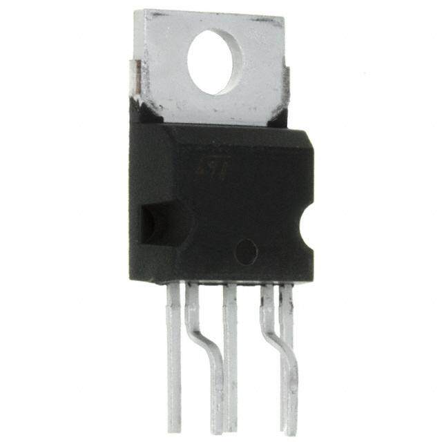
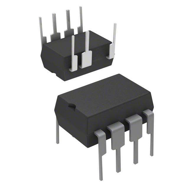
| 描述 | IC OFFLINE CTRLR PWM PROG 18DIP交流/直流转换器 Prog Off-Line PWM Controller |
| 产品分类 | |
| 品牌 | Texas Instruments |
| 产品手册 | |
| 产品图片 |
|
| rohs | 符合RoHS无铅 / 符合限制有害物质指令(RoHS)规范要求 |
| 产品系列 | 电源管理 IC,交流/直流转换器,Texas Instruments UC3851N- |
| 数据手册 | http://www.ti.com/lit/pdf/slus226 |
| 产品型号 | UC3851N |
| 产品目录页面 | |
| 产品种类 | 交流/直流转换器 |
| 供应商器件封装 | 18-PDIP |
| 其它名称 | 296-11305-5 |
| 功率(W) | - |
| 包装 | 管件 |
| 单位重量 | 1.206 g |
| 占空比-最大 | 46 % |
| 商标 | Texas Instruments |
| 安装风格 | Through Hole |
| 封装 | Tube |
| 封装/外壳 | 18-DIP(0.300",7.62mm) |
| 封装/箱体 | PDIP-18 |
| 工作温度 | 0°C ~ 70°C |
| 工作温度范围 | 0 C to + 70 C |
| 工厂包装数量 | 20 |
| 开关频率 | 50 kHz to 500 kHz |
| 拓扑结构 | Boost, Buck, Flyback, Forward |
| 标准包装 | 20 |
| 电压-击穿 | - |
| 电压-输入 | 8 V ~ 32 V |
| 电压-输出 | 40V |
| 电源电流 | 15 mA |
| 类型 | Current Mode PWM Controllers |
| 系列 | UC3851 |
| 绝缘 | Non-Isolated |
| 输入/电源电压—最大值 | 30 V |
| 输入/电源电压—最小值 | 8 V |
| 输出功率 | 1 W |
| 输出电压 | 40 V |
| 输出电流 | 400 mA |
| 输出端数量 | 1 Output |
| 输出隔离 | 任意一种 |
| 频率范围 | 45kHz ~ 55kHz |


- 商务部:美国ITC正式对集成电路等产品启动337调查
- 曝三星4nm工艺存在良率问题 高通将骁龙8 Gen1或转产台积电
- 太阳诱电将投资9.5亿元在常州建新厂生产MLCC 预计2023年完工
- 英特尔发布欧洲新工厂建设计划 深化IDM 2.0 战略
- 台积电先进制程称霸业界 有大客户加持明年业绩稳了
- 达到5530亿美元!SIA预计今年全球半导体销售额将创下新高
- 英特尔拟将自动驾驶子公司Mobileye上市 估值或超500亿美元
- 三星加码芯片和SET,合并消费电子和移动部门,撤换高东真等 CEO
- 三星电子宣布重大人事变动 还合并消费电子和移动部门
- 海关总署:前11个月进口集成电路产品价值2.52万亿元 增长14.8%


PDF Datasheet 数据手册内容提取
UC1851 UC2851 UC3851 Programmable, Off-Line, PWM Controller FEATURES DESCRIPTION • All Control, Driving, Monitoring, and Protection The UC1851 family of PWM controllers are optimized for off- Functions Included line primary side control. These devices include a high current totem pole output stage and a toggle flip-flop for absolute 50% • Low-Current Off Line Start Circuit duty cycle limiting. In all other respects this line of controllers is • Voltage Feed Forward or Current Mode Control pin for pin compatible with the UC1841 series. Inclusion of all major housekeeping functions in these high performance con- • High Current Totem Pole Output trollers makes them ideal for use in cost sensitive applications. • 50% Absolute Max Duty Cycle Important features of these controllers include low current • PWM Latch for Single Pulse Per Period start-up, linear feed-forward for constant volt-second operation, and compatibility with both voltage or current mode control. In • Pulse-by-Pulse Current Limiting plus Shutdown addition, these devices include a programmable start thresh- for Over-Current Fault old, as well as programmable over-voltage, under-voltage, and • No Start-Up or Shutdown Transients over current fault thresholds. The fault latch on these devices can be configured for automatic restart, or latched off response • Slow Turn-On Both Initially and After Fault to a fault. Shutdown These devices are packaged in 18-pin plastic or ceramic dual- • Shutdown Upon Over or Under Voltage Sensing in-line packages, or for surface mount applications, a 20 Pin • Latch Off or Continuous Retry After Fault PLCC. The UC1851 is characterized for -55(cid:176) C to +125(cid:176) C op- eration while the UC2851 and UC3851 are designed for -40(cid:176) C • 1% Reference Accuracy to +85(cid:176) C and 0(cid:176) C to +70(cid:176) C, respectively. • 500kHz Operation • 18 Pin DIL or 20 Pin PLCC Package BLOCK DIAGRAM 10/94
UC1851 UC2851 UC3851 ABSOLUTE MAXIMUM RATINGS (Note 1) Supply Voltage, +VIN (Pin 15) Comparator Inputs Voltage Driven. . . . . . . . . . . . . . . . . . . . . . . . . . . . . . . . +32V (Pins 1–7, 9–11, 16). . . . . . . . . . . . . . Internally clamped at 12V Current Driven, 100mA maximum. . . . . . . . . . . Self-limiting Power Dissipation at TA = 25°C (Note 3). . . . . . . . . . . 1000mW PWM Output Voltage (Pin 12) . . . . . . . . . . . . . . . . . . . . . . . 40V Power Dissipation at TC = 25°C (Note 3). . . . . . . . . . . 2000mW PWM Output Current, Steady-State (Pin 12). . . . . . . . . 400mA Operating Junction Temperature. . . . . . . . . . . -55°C to +150°C PWM Output Peak Energy Discharge . . . . . . . . . . . . 20m Joules Storage Temperature Range. . . . . . . . . . . . . . -65°C to +150°C Driver Bias Current (Pin 14). . . . . . . . . . . . . . . . . . . . . -200mA Lead Temperature (Soldering, 10 sec) . . . . . . . . . . . . . +300°C Reference Output Current (Pin 16) . . . . . . . . . . . . . . . . -50mA Note 1:All voltages are with respect to ground, Pin 13. Slow-Start Sink Current (Pin 8) . . . . . . . . . . . . . . . . . . . . 20mA Currents are positive-into, negative-out of the VIN Sense Current (Pin 11). . . . . . . . . . . . . . . . . . . . . . . . 10mA specified terminal Current Limit Inputs (Pins 6 & 7) . . . . . . . . . . . . . -0.5 to +5.5V Note 2:All pin numbers are referenced to DIL-18 package. Stop Input (Pin 4). . . . . . . . . . . . . . . . . . . . . . . . . -0.3 to +5.5V Note 3:Consult Packaging Section of Databook for thermal limitations and considerations of package. CONNECTION DIAGRAMS DIL-18, SOIC-18 (TOP VIEW) PLCC-20, LCC-20 PACKAGE PIN FUNCTIONS J or N, DW Package (TOP VIEW) FUNCTION PIN Q, L PACKAGE COMP 1 START/UV 2 OV SENSE 3 STOP 4 RESET 5 CUR THRESH 7 CUR SENSE 8 SLOW START 9 RT/CT 10 RAMP 11 VIN SENSE 12 PWM OUT 13 GROUND 14 DRIVE BIAS 15 +VIN SUPPLY 17 5.0V REF 18 INV. INPUT 19 N.I. INPUT 20 ELECTRICAL CHARACTERISTICS: Unless otherwise stated, these specifications apply for TA = -55°C to +125°C for the UC1851, -40°C to +85°C for the UC2851, and 0°C to 70°C for the UC3851; VIN = 20V, RT = 20kW , CT = .001 mfd, RR = 10kW , CR = .001mfd. Current Limit Threshold = 200mV, TA = TJ. UC1851 / UC2851 UC3851 UNITS PARAMETER TEST CONDITIONS MIN TYP MAX MIN TYP MAX Power Inputs Start-Up Current VIN = 30V, Pin 2 = 2.5V 4.5 6 4.5 6 mA Operating Current VIN = 30V, Pin 2 = 3.5V 15 21 15 21 mA Supply OV Clamp VIN = 20mA 33 39 45 33 39 45 V Reference Section Reference Voltage TJ = 25°C 4.95 5.0 5.05 4.9 5.0 5.1 V Line Regulation VIN = 8 to 30V 10 15 10 20 mV Load Regulation IL = 0 to 10mA 10 20 10 30 mV Total Ref Variation Over Operating Temperature Range 4.9 5.1 4.85 5.15 V Short Circuit Current VREF = 0, TJ = 25°C -80 -100 -80 -100 mA Oscillator Nominal Frequency TJ = 25°C 47 50 53 45 50 55 kHz Voltage Stability VIN = 8 to 30V 0.5 1 0.5 1 % Total Ref Variation Over Operating Temperature Range 45 55 43 57 kHz Maximum Frequency RT = 2kW , CT = 330pF 500 500 kHz 2
UC1851 UC2851 UC3851 ELECTRICAL CHARACTERISTICS: Unless otherwise stated, these specifications apply for TA = -55°C to +125°C for the UC1851, -40°C to +85°C for the UC2851, and 0°C to 70°C for the UC3851; VIN = 20V, RT = 20kW , CT = .001 mfd, RR = 10kW , CR = .001mfd. Current Limit Threshold = 200mV, TA = TJ. PARAMETER TEST CONDITIONS UC1851 / UC2851 UC3851 UNITS MIN TYP MAX MIN TYP MAX Ramp Generator Ramp Current, Minimum ISENSE = - 10m A -11 -14 -11 -14 m A Ramp Current, Maximum ISENSE = 1.0mA -0.9 -.95 -0.9 -.95 mA Ramp Valley 0.3 0.4 0.6 0.3 0.4 0.6 V Ramp Peak Clamping Level 3.9 4.2 4.5 3.9 4.2 4.5 V Error Amplifier Input Offset Voltage VCM = 5.0V 0.5 5 2 10 mV Input Bias Current 0.5 2 1 5 m A Input Offset Current 0.5 0.5 m A Open Loop Gain D VO = 1 to 3V 60 66 60 66 dB Output Swing (Max Output £ Minimum Total Range 0.3 3.5 0.3 3.5 V Ramp Peak - 100mV) CMRR VCM = 1.5 to 5.5V 70 80 70 80 dB PSRR VIN = 8 to 30V 70 80 70 80 dB Short Circuit Current VCOMP = 0V -4 -10 -4 -10 mA Gain Bandwidth (Note 1) TJ = 25°C, AVOL = 0dB 1 2 1 2 MHz Slew Rate (Note 1) TJ = 25°C, AVCL = 0dB 0.8 0.8 V/m s PWM Section Continuous Duty Cycle Range Minimum Total Continuous Range 2 46 2 46 % (other than zero) (Note 1) Ramp Peak < 4.2V Output High Level ISOURCE = 20mA 18 18.5 18 18.5 V ISOURCE = 200mA 17 18.5 17 18.5 V Rise Time (Note 1) TJ = 25°C, CL = 1nF 50 150 50 150 ns Fall Time (Note 1) TJ = 25°C, CL = 1nF 50 150 50 150 ns Output Saturation IOUT = 20mA 0.2 0.4 0.2 0.4 V IOUT = 200mA 1.7 2.2 1.7 2.2 V Comparator Delay (Note 1) Pin 8 to Pin 12, TJ = 25°C, RL = 1kW 300 500 300 500 ns Sequencing Functions Comparator Thresholds Pins 2, 3, 5 2.8 3.0 3.2 2.8 3.0 3.2 V Input Bias Current Pins 3, 5 = 0V -1.0 -4.0 -1.0 -4.0 m A Input Leakage Pins 3, 5 = 10V 0.1 2.0 0.1 2.0 m A Start/UV Hysteresis Current Pin 2 = 2.5V 170 200 220 170 200 230 m A Ext. Stop Threshold Pin 4 0.8 1.6 2.4 0.8 1.6 2.4 V Error Latch Activate Current Pin 4 = 0V, Pin 3 > 3V -120 -200 -120 -200 m A Driver Bias Saturation Voltage, IB = -50mA 2 3 2 3 V VIN-VOH Driver Bias Leakage VB = 0V -0.1 -10 -0.1 -10 m A Slow-Start Saturation IS = 10mA 0.2 0.5 0.2 0.5 V Slow-Start Leakage VS = 4.5V 0.1 2.0 0.1 2.0 m A Current Control Current Limit Offset 0 5 0 10 mV Current Shutdown Offset 370 400 430 360 400 440 mV Input Bias Current Pin 7 = 0V -2 -5 -2 -5 m A Common Mode Range (Note 1) -0.4 3.0 -0.4 3.0 V Current Limit Delay (Note 1) TJ = 25°C, Pin 7 to 12, RL = 1k 200 400 200 400 ns Note 1:Guaranteed by design. Not 100% tested in production. 3
UC1851 UC2851 UC3851 FUNCTIONAL DESCRIPTION PWM CONTROL 1. Oscillator Generates a fixed-frequency internal clock from an external RT and CT. Frequency = KC where KC is a first-order correction factor » 0.3 log (CT x 1012). RTCT 2. Ramp Generator: Develops linear ramp with slope defined externally by dV = sense voltage. dT RRCR CR is normally selected £ CT and its value will have some effect upon valley duty cycle. Limiting the minimum value for ISENSE into pin 11 will establish a maximum duty cycle clamp. CR terminal can be used as an input port for current mode control. 3. Error Amplifier Conventional operational amplifier for closed-loop gain and phase compensation. Low output impedance; unity-gain stable. The output is held low by the slow start voltage at turn on in order to minimize overshoot. 4. Reference Generator: Precision 5.0V for internal and external usage to 50mA. Tracking 3.0V reference for internal usage only with nominal accuracy of – 2%. 40V clamp zener for chip OV protection, 100mA maximum current. 5. PWM Comparator: Generates output pulse which starts at termination of clock pulse and ends when the ramp input crosses the lowest of two positive inputs. 6. PWM Latch: Terminates the PWM output pulse when set by inputs from either the PWM comparator, the pulse-by-pulse comparator, or the error latch. Resets with each internal clock pulse. 7. PWM Output Switch: Totem pole output stage capable of sourcing and sinking 1 amp peak current. The active "on" state is high. SEQUENCING FUNCTIONS 1. Start/UV Sense: With an increasing voltage, this comparator generates a turn-on signal and releases the slow start clamp at a start threshold. With a decreasing voltage, it generates a turn-off command at a lower level separated by a 200m A hysteresis current. 2. Drive Switch: Disables most of the chip to hold internal current consumption low, and Driver Bias OFF, until input voltage reaches start threshold. 3. Driver Bias: Supplies drive to external circuitry upon start-up. 4. Slow Start: Clamps low to hold PWM OFF. Upon release, rises with rate controlled by RSCS for slow increase of output pulse width. Can also be used as an alternate maximum duty cycle clamp with an external voltage divider. PROTECTION FUNCTIONS 1. Error Latch: When set by momentary input, this latch insures immediate PWM shutdown and hold off until reset. Inputs to Error Latch are: a. OV > 3.2V (Typically 3V) b. Stop > 2.4V (Typically 1.6V) c. Current Sense 400mV over threshold. (Typical). Error Latch resets when slow start voltage falls to 0.4V if Reset Pin < 2.8V. With Pin 5 > 3.2V, Error Latch will remain set. 2. Current Limiting: Differential input comparator terminates individual output pulses each time sense voltage rises above threshold. When sense voltage rises to 400mV (typical) above threshold, a shutdown signal is sent to Error Latch. 3. External Stop: A voltage over 2.4 will set the Error Latch and hold the output off. A voltage less than 0.8V will defeat the error latch and prevent shutdown. A capacitor here will slow the action of the error latch for transient protection by providing a Typical Delay of 13ms/m F. 4
UC1851 UC2851 UC3851 Start/UV Hysteresis Current Output Saturation Characteristics Oscillator Frequency PWM Output Minimum Pulse Width Error Amplifier Open-Loop Gain and Phase Shutdown Timing 5
UC1851 UC2851 UC3851 OPEN-LOOP CIRCUIT 1 (cid:230) R1 + R2 + R3(cid:246) Current Limit = 200mV Nominal Frequency = = 50kHz UV Fault Voltage = 3 (cid:231) (cid:247) = 8V RTCT Ł R2 + R3 ł Current Fault Voltage = 600mV Start Voltage = 3 (cid:230)(cid:231)Ł R1R +2 R +2 R +3 R3(cid:246)(cid:247)ł +0.2R1 = 12V OV Fault Voltage = 3 (cid:230)(cid:231)Ł R1 + RR32 + R3(cid:246)(cid:247)ł = 32V Duty Cycle Clamp = 50% @VIN = 15V, Duty Cycle = 48% @VIN = 30V, Duty Cycle = 24% High Peak currents associated with capacitive loads necessitate careful grounding techniques. Timing and bypass capacitors should be connected close to pin 13 in a single ground point. Programmable Soft Start and Restart Delay Circuit UC1851 Power MOSFET Drive Interface For further application information see UC1840/UC1841 Data Sheets UNITRODE INTEGRATED CIRCUITS 7 CONTINENTAL BLVD. • MERRIMACK, NH 03054 TEL. (603) 424-2410 • FAX (603) 424-3460 6
PACKAGE OPTION ADDENDUM www.ti.com 18-Sep-2008 PACKAGING INFORMATION OrderableDevice Status(1) Package Package Pins Package EcoPlan(2) Lead/BallFinish MSLPeakTemp(3) Type Drawing Qty 5962-9558601MVA OBSOLETE CDIP J 18 TBD CallTI CallTI UC1851J OBSOLETE CDIP J 18 TBD CallTI CallTI UC1851J883B OBSOLETE CDIP J 18 TBD CallTI CallTI UC2851DW ACTIVE SOIC DW 18 40 Green(RoHS& CUNIPDAU Level-2-260C-1YEAR noSb/Br) UC2851DWG4 ACTIVE SOIC DW 18 40 Green(RoHS& CUNIPDAU Level-2-260C-1YEAR noSb/Br) UC2851N ACTIVE PDIP N 18 20 Green(RoHS& CUNIPDAU N/AforPkgType noSb/Br) UC2851NG4 ACTIVE PDIP N 18 20 Green(RoHS& CUNIPDAU N/AforPkgType noSb/Br) UC3851DW ACTIVE SOIC DW 18 40 Green(RoHS& CUNIPDAU Level-2-260C-1YEAR noSb/Br) UC3851DWG4 ACTIVE SOIC DW 18 40 Green(RoHS& CUNIPDAU Level-2-260C-1YEAR noSb/Br) UC3851DWTR ACTIVE SOIC DW 18 2000 Green(RoHS& CUNIPDAU Level-2-260C-1YEAR noSb/Br) UC3851DWTRG4 ACTIVE SOIC DW 18 2000 Green(RoHS& CUNIPDAU Level-2-260C-1YEAR noSb/Br) UC3851N ACTIVE PDIP N 18 20 Green(RoHS& CUNIPDAU N/AforPkgType noSb/Br) UC3851NG4 ACTIVE PDIP N 18 20 Green(RoHS& CUNIPDAU N/AforPkgType noSb/Br) (1)Themarketingstatusvaluesaredefinedasfollows: ACTIVE:Productdevicerecommendedfornewdesigns. LIFEBUY:TIhasannouncedthatthedevicewillbediscontinued,andalifetime-buyperiodisineffect. NRND:Notrecommendedfornewdesigns.Deviceisinproductiontosupportexistingcustomers,butTIdoesnotrecommendusingthispartin anewdesign. PREVIEW:Devicehasbeenannouncedbutisnotinproduction.Samplesmayormaynotbeavailable. OBSOLETE:TIhasdiscontinuedtheproductionofthedevice. (2)EcoPlan-Theplannedeco-friendlyclassification:Pb-Free(RoHS),Pb-Free(RoHSExempt),orGreen(RoHS&noSb/Br)-pleasecheck http://www.ti.com/productcontentforthelatestavailabilityinformationandadditionalproductcontentdetails. TBD:ThePb-Free/Greenconversionplanhasnotbeendefined. Pb-Free(RoHS):TI'sterms"Lead-Free"or"Pb-Free"meansemiconductorproductsthatarecompatiblewiththecurrentRoHSrequirements forall6substances,includingtherequirementthatleadnotexceed0.1%byweightinhomogeneousmaterials.Wheredesignedtobesoldered athightemperatures,TIPb-Freeproductsaresuitableforuseinspecifiedlead-freeprocesses. Pb-Free(RoHSExempt):ThiscomponenthasaRoHSexemptionforeither1)lead-basedflip-chipsolderbumpsusedbetweenthedieand package, or 2) lead-based die adhesive used between the die and leadframe. The component is otherwise considered Pb-Free (RoHS compatible)asdefinedabove. Green(RoHS&noSb/Br):TIdefines"Green"tomeanPb-Free(RoHScompatible),andfreeofBromine(Br)andAntimony(Sb)basedflame retardants(BrorSbdonotexceed0.1%byweightinhomogeneousmaterial) (3) MSL, Peak Temp. -- The Moisture Sensitivity Level rating according to the JEDEC industry standard classifications, and peak solder temperature. Important Information and Disclaimer:The information provided on this page represents TI's knowledge and belief as of the date that it is provided. TI bases its knowledge and belief on information provided by third parties, and makes no representation or warranty as to the accuracy of such information. Efforts are underway to better integrate information from third parties. TI has taken and continues to take reasonable steps to provide representative and accurate information but may not have conducted destructive testing or chemical analysis on incomingmaterialsandchemicals.TIandTIsuppliersconsidercertaininformationtobeproprietary,andthusCASnumbersandotherlimited informationmaynotbeavailableforrelease. Addendum-Page1
PACKAGE OPTION ADDENDUM www.ti.com 18-Sep-2008 InnoeventshallTI'sliabilityarisingoutofsuchinformationexceedthetotalpurchasepriceoftheTIpart(s)atissueinthisdocumentsoldbyTI toCustomeronanannualbasis. Addendum-Page2
PACKAGE MATERIALS INFORMATION www.ti.com 6-Nov-2008 TAPE AND REEL INFORMATION *Alldimensionsarenominal Device Package Package Pins SPQ Reel Reel A0(mm) B0(mm) K0(mm) P1 W Pin1 Type Drawing Diameter Width (mm) (mm) Quadrant (mm) W1(mm) UC3851DWTR SOIC DW 18 2000 330.0 24.4 10.9 12.0 2.7 12.0 24.0 Q1 PackMaterials-Page1
PACKAGE MATERIALS INFORMATION www.ti.com 6-Nov-2008 *Alldimensionsarenominal Device PackageType PackageDrawing Pins SPQ Length(mm) Width(mm) Height(mm) UC3851DWTR SOIC DW 18 2000 346.0 346.0 41.0 PackMaterials-Page2
IMPORTANTNOTICE TexasInstrumentsIncorporatedanditssubsidiaries(TI)reservetherighttomakecorrections,modifications,enhancements,improvements, andotherchangestoitsproductsandservicesatanytimeandtodiscontinueanyproductorservicewithoutnotice.Customersshould obtainthelatestrelevantinformationbeforeplacingordersandshouldverifythatsuchinformationiscurrentandcomplete.Allproductsare soldsubjecttoTI’stermsandconditionsofsalesuppliedatthetimeoforderacknowledgment. TIwarrantsperformanceofitshardwareproductstothespecificationsapplicableatthetimeofsaleinaccordancewithTI’sstandard warranty.TestingandotherqualitycontroltechniquesareusedtotheextentTIdeemsnecessarytosupportthiswarranty.Exceptwhere mandatedbygovernmentrequirements,testingofallparametersofeachproductisnotnecessarilyperformed. TIassumesnoliabilityforapplicationsassistanceorcustomerproductdesign.Customersareresponsiblefortheirproductsand applicationsusingTIcomponents.Tominimizetherisksassociatedwithcustomerproductsandapplications,customersshouldprovide adequatedesignandoperatingsafeguards. TIdoesnotwarrantorrepresentthatanylicense,eitherexpressorimplied,isgrantedunderanyTIpatentright,copyright,maskworkright, orotherTIintellectualpropertyrightrelatingtoanycombination,machine,orprocessinwhichTIproductsorservicesareused.Information publishedbyTIregardingthird-partyproductsorservicesdoesnotconstitutealicensefromTItousesuchproductsorservicesora warrantyorendorsementthereof.Useofsuchinformationmayrequirealicensefromathirdpartyunderthepatentsorotherintellectual propertyofthethirdparty,oralicensefromTIunderthepatentsorotherintellectualpropertyofTI. ReproductionofTIinformationinTIdatabooksordatasheetsispermissibleonlyifreproductioniswithoutalterationandisaccompanied byallassociatedwarranties,conditions,limitations,andnotices.Reproductionofthisinformationwithalterationisanunfairanddeceptive businesspractice.TIisnotresponsibleorliableforsuchaltereddocumentation.Informationofthirdpartiesmaybesubjecttoadditional restrictions. ResaleofTIproductsorserviceswithstatementsdifferentfromorbeyondtheparametersstatedbyTIforthatproductorservicevoidsall expressandanyimpliedwarrantiesfortheassociatedTIproductorserviceandisanunfairanddeceptivebusinesspractice.TIisnot responsibleorliableforanysuchstatements. TIproductsarenotauthorizedforuseinsafety-criticalapplications(suchaslifesupport)whereafailureoftheTIproductwouldreasonably beexpectedtocauseseverepersonalinjuryordeath,unlessofficersofthepartieshaveexecutedanagreementspecificallygoverning suchuse.Buyersrepresentthattheyhaveallnecessaryexpertiseinthesafetyandregulatoryramificationsoftheirapplications,and acknowledgeandagreethattheyaresolelyresponsibleforalllegal,regulatoryandsafety-relatedrequirementsconcerningtheirproducts andanyuseofTIproductsinsuchsafety-criticalapplications,notwithstandinganyapplications-relatedinformationorsupportthatmaybe providedbyTI.Further,BuyersmustfullyindemnifyTIanditsrepresentativesagainstanydamagesarisingoutoftheuseofTIproductsin suchsafety-criticalapplications. TIproductsareneitherdesignednorintendedforuseinmilitary/aerospaceapplicationsorenvironmentsunlesstheTIproductsare specificallydesignatedbyTIasmilitary-gradeor"enhancedplastic."OnlyproductsdesignatedbyTIasmilitary-grademeetmilitary specifications.BuyersacknowledgeandagreethatanysuchuseofTIproductswhichTIhasnotdesignatedasmilitary-gradeissolelyat theBuyer'srisk,andthattheyaresolelyresponsibleforcompliancewithalllegalandregulatoryrequirementsinconnectionwithsuchuse. TIproductsareneitherdesignednorintendedforuseinautomotiveapplicationsorenvironmentsunlessthespecificTIproductsare designatedbyTIascompliantwithISO/TS16949requirements.Buyersacknowledgeandagreethat,iftheyuseanynon-designated productsinautomotiveapplications,TIwillnotberesponsibleforanyfailuretomeetsuchrequirements. FollowingareURLswhereyoucanobtaininformationonotherTexasInstrumentsproductsandapplicationsolutions: Products Applications Amplifiers amplifier.ti.com Audio www.ti.com/audio DataConverters dataconverter.ti.com Automotive www.ti.com/automotive DSP dsp.ti.com Broadband www.ti.com/broadband ClocksandTimers www.ti.com/clocks DigitalControl www.ti.com/digitalcontrol Interface interface.ti.com Medical www.ti.com/medical Logic logic.ti.com Military www.ti.com/military PowerMgmt power.ti.com OpticalNetworking www.ti.com/opticalnetwork Microcontrollers microcontroller.ti.com Security www.ti.com/security RFID www.ti-rfid.com Telephony www.ti.com/telephony RF/IFandZigBee®Solutions www.ti.com/lprf Video&Imaging www.ti.com/video Wireless www.ti.com/wireless MailingAddress:TexasInstruments,PostOfficeBox655303,Dallas,Texas75265 Copyright©2008,TexasInstrumentsIncorporated