首页 > UC3846N > 详情
 Datasheet下载
- 型号: UC3846N
- 制造商: Texas Instruments
- 库位|库存: xxxx|xxxx
- 要求:
| 数量阶梯 | 香港交货 | 国内含税 |
| +xxxx | $xxxx | ¥xxxx |
查看当月历史价格
查看今年历史价格
产品参数
| 参数 | 数值 |
| 产品目录 | 集成电路 (IC)半导体 |
| Cuk | 无 |
| 描述 | IC REG CTRLR PWM CM 16DIP开关控制器 Current-Mode PWM Controller |
| 产品分类 | PMIC - 稳压器 - DC DC 切换控制器集成电路 - IC |
| 品牌 | Texas Instruments |
| 产品手册 | 点击此处下载产品Datasheet |
| 产品图片 |   |
| rohs | 符合RoHS无铅 / 符合限制有害物质指令(RoHS)规范要求 |
| 产品系列 | 电源管理 IC,开关控制器 ,Texas Instruments UC3846N- |
| 数据手册 | 点击此处下载产品Datasheet |
| 产品型号 | UC3846N |
| PWM类型 | 电流模式 |
| 上升时间 | 50 ns |
| 下降时间 | 50 ns |
| 产品目录页面 | 点击此处下载产品Datasheet |
| 产品种类 | 开关控制器 |
| 倍增器 | 无 |
| 其它名称 | 296-11301-5 |
| 分频器 | 无 |
| 包装 | 管件 |
| 升压 | 是 |
| 单位重量 | 1.054 g |
| 占空比 | 50% |
| 占空比-最大 | 50 % |
| 反向 | 无 |
| 反激式 | 是 |
| 商标 | Texas Instruments |
| 安装风格 | Through Hole |
| 封装 | Tube |
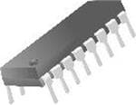
| 封装/外壳 | 16-DIP(0.300",7.62mm) |
| 封装/箱体 | PDIP-16 |
| 工作温度 | 0°C ~ 70°C |
| 工厂包装数量 | 25 |
| 开关频率 | 450 kHz |
| 拓扑结构 | Buck, Boost, Flyback, Forward, Full-Bridge, Half-Bridge, Push-Pull |
| 最大工作温度 | + 70 C |
| 最小工作温度 | 0 C |
| 标准包装 | 25 |
| 电压-电源 | 7.7 V ~ 40 V |
| 类型 | Current Mode PWM Controllers |
| 系列 | UC3846 |
| 输出数 | 2 |
| 输出电流 | 500 mA |
| 输出端数量 | 2 Output |
| 降压 | 是 |
| 隔离式 | 无 |
| 频率-最大值 | 500kHz |
Datasheet
PDF Datasheet 数据手册内容提取
www.fairchildsemi.com UC3846 SMPS Controller Features Description • Automatic Feed Forward Compensation The UC3846 control IC provides all of the necessary fea- • Programmable Pulse by Pulse Current Limiting tures to implement fixed frequency, current mode control • Automatic Symmetry Correction in Push-Pull schemes while maintaining a minimum external parts count. Configuration The superior performance of this technique can be measured • Enhanced Load Response Characteristics in improved line regulation, enhanced load response char- • Parallel Operation Capability for Modulator Power acteristics, and a simpler, easier-to-design control loop. Systems Topological advantages include inherent pulse-by-pulse cur- • Differential Current Sense Amplifier with Common Mode rent limiting capability, automatic symmetry correction for Range push-pull converters, and the ability to parallel “power • Double Pulse Suppression module,, while maintaining equal current sharing. Protection • 200mA Totem-Pole Outputs circuitry includes built-in-under-voltage lockout and pro- • ±2% Band gap Reference grammable current limit in addition to soft-start capability. A • Under-Voltage Lockout shutdown function is also available which can initiate either • Soft-Start Capability a complete shutdown with automatic restart or latch the • Shutdown Terminal supply off. Other features include fully latched operation, • 500KHz Operation double pulse suppression, deadtime adjust capability, and ±2% trimmed bandgap reference. The UC3846 features low outputs in the OFF state. 16-DIP 1 Internal Block Diagram 10 Rev. 5.0 ©2000 Fairchild Semiconductor International
UC3846 Absolute Maximum Ratings Parameter Symbol Value Unit Supply Voltage VCC 40 V Collector Supply Voltage VC 40 V Output Current, Sink of Source (Peak) IO 500 mA Reference Output Current IREF 30 mA Soft Start Sink Current ISINK(S.S) 50 mA Sync Output Current ISYNC 5 mA Error Amplifier Output Current IO(E.A) 5 mA Oscillator Changing Current ICHG(OSC) 5 mA Power Dissipation (TA = 25°C) PD 1000 mW Operating Temperature TOPR 0 ~ +70 °C Storage Temperature TSTG -65 ~ +150 °C Lead Temperature (Soldering, 10sec) TLEAD +300 °C Electrical Characteristics (VCC=15V, TA=0°C to +70°C, unless otherwise specified) Parameter Symbol Conditions Min. Typ. Max. Unit REFERENCE SECTION Reference Output Voltage VREF TJ = 25°C, IREF = 1mA 5.00 5.10 5.20 V Line Regulation ∆VREF VCC = 8 to 40V - 5 20 mV Load Regulation ∆VREF IREF1 to 10mA - 3 15 mV Temperature Stability(Note 6) STT - - 0.4 1.0 mV/°C Output Voltage Range (Note 6) VREF Line,Load,Temp 4.95 - 5.25 V Short Circuit Output Current ISC VREF = 0V -10 -45 - mA Output Noise Voltage(Note 6) VNO f = 10Hz to 10KHz, TJ = 25°C - 100 - uV Long-Term Stability(Note 6) ST TJ = 125°C, 1KHz 2 5 8 mV 2
UC3846 Electrical Characteristics (VCC= 15V,TA=0°C to +70°C, unless otherwise specified) Parameter Symbol Conditions Min. Typ. Max. Unit OSCILLATOR SECTION (Note 2) Initial Accuracy ACCUR TJ = 25°C 39 43 47 KHz Frequency Change with Voltage ∆f/∆VCC VCC = 8 to 40V - 1 2 % Frequency Change with ∆f/∆T - - 1 - % Temperature (Note 6) Sync Output High Level VOH(SYNC) - 3.9 4.35 - V Sync Output Low Level VOL(SYNC) - - 2.3 2.5 V Sync Input High Level VIH(SYNC) V8 = 0V 3.9 - - V Sync Input Low Level VIL(SYNC) V8 = 0V - - 2.5 V Sync Input Current II(SYNC) Sync Voltage = 3.9V, V8 = 0V - 1.3 1.5 mA ERROR AMPLIFIER SECTION Input Offset Voltage VIO - - 0.5 5 mV Input Bias Current IBIAS - - -0.6 -1 uA Input Offset Current IIO - - 40 250 uA Common-Mode Range VCM VCC = 8 to 40V 0 - VCC2 V Open Loop Voltage Gain GVO VO = 1.2 to 3V, VCM = 2V 80 105 - dB Unity Gain Bandwidth(Note 6) BW TJ = 25°C 0.7 1.0 - MHz Common Mode Rejection Ratio CMRR VCM = 0 to 38V, VCC = 40V 75 100 - dB Power Supply Rejection Ratio PSRR VCC = 8 to 40V 80 105 - dB Output Sink Current ISINK VIO = -15mV to 5V, V7 = 2.5V 2 6 - mA Output Source Current ISOURCE RL = 15KΩ -0.4 -0.5 - mA High Output Voltage VOH RL = 15KΩ 4.3 4.6 - V Low Output Voltage VOL - - 0.7 1 V CURRENT SENSE AMPLIFIER SECTION Amplifier Gain (Note 1, 3) GV V3 = 0V, Pin 1 open 2.5 2.75 3.0 V Maximum Differential Input VI(DIFF,MAX) RL = 15KΩ, Pin 1 open 1.1 1.2 - V Signal (V4 - V3) (Note 1) Input Offset Voltage (Note 1) VIO V1 = 0.5V, Pin 1 open - 5 25 mV Common Mode Rejection Ratio CMRR VCM = 1 to 12V 60 83 - dB Power Supply Rejection Ratio PSRR VCC = 8 to 40V 60 84 - dB Input Bias Current (Note 1) IBIAS V1 = 0.5V, Pin 7 open - -2.5 -10 uA Input Offset Current (Note 1) IIO V1 = 0.5V, Pin 7 open - 0.08 1 uA Delay to Outputs (Note 6) tD TJ = 25°C - 200 500 ns 3
UC3846 Electrical Characteristics (VCC=15V, TA=0°C to + 70°C, unless otherwise specified) Parameter Symbol Conditions Min. Typ. Max. Unit CURRENT LIMIT ADJUST SECTION Current Limit Offset Voltage (Note 1) VIO(C.L) V3 = 0V 0.45 0.5 0.55 V V4 = 0V, Pin 7 open Input Bias Current IBIAS V5 = VREF, V6 = 0V - - 10 - 30 uA SHUTDOWN TERMINAL SECTION Threshold Voltage VTH - 250 350 400 mV Input Voltage Range VI - 0 - VCC V Minimum Latching Current (Note 4) I(LATCH,MIN) - 3.0 1.5 - mA Maximum Non-Latching Current (Note 5) I(NONLATCH,MAX) - - 1.5 0.8 mA UNDER-VOLTAGE LOCKOUT SECTION Start Threshold VTH(ST) - 7 7.7 8.4 V Threshold Hysteresis VHYS - 0.45 0.75 1.05 V OUTPUT SECTION Collector-Emitter Voltage VCEO - 40 - - V Collector Leakage Current ILEAK VC = 40V - - 200 uA Low Output Voltage 1 VOL 1 ISINK = 20mA - 0.1 0.4 V Low Output Voltage 2 VOL 2 ISINK = 100mA - 0.4 2.1 V High Output Voltage 1 VOH 1 ISOURCE = 20mA 13 13.5 - V High Output Voltage 2 VOH 2 ISOURCE = 100mA 12 13.5 - V Rise Time (Note 6) tR CL = 1nF, TJ = 25°C - 50 300 us Fall Time (Note 6) tF CL = 1nF, TJ = 25°C - 50 300 us TOTAL STANDBY CURRENT Supply Current ICC - - 17 21 mA Notes : 1. Parameter measured at trip point at latch with V5 = VREF, V6 = 0V 2. RT = 10KΩ, CT = 4.7nF 3. Amplifier gain definde as: ∆V7 G= -----------;∆V = 0to1.0V ∆V4 4 4. Current into Pin 1 guaranteed to latch circuit in shutdown state. 5. Current into Pin 1 guaranteed not to latch circuit in shutdown state. 6. These parameters, although guaranteed over the recommended operating conditions, are not 100% tested in production. 4
UC3846 Td OUTPUT DEADTIME(Td) Figure 1.UC3846 Oscillator Circuit 12 Output deadtime is determined by the external capacitor, CT, according to the formula: Td(us)= 145C (µF)---------------------------------- T 3.6 For large values of RT: Td (us) = l45CT (uF) Oscillator frequency is approximately 12–-R-------(---K----Ω------) T by the formula: f (KHz)= -----------------2----.-2-------------------- T R (KΩ)C (µF) T T Figure 2.Error Amplifier Output Configuration 5
UC3846 Figure 3.Parallel Operation Figure 4.Pulse By Pulse Current Limiting Figure 5.Current Sense Amp Connections A small PC filter may be required in some applications to reduce switch transients Differential input allows remote, noise free sensing. 6
UC3846 Mechanical Dimensions Package 16-DIP 6.40 ±0.20 ) 0.252 ±0.008 0.81 0.032 ( #1 #16 4 4 ±6 0.10 ±8 0.00 ±0 0.10 ±9 0.00 19.80MAX0.780 ±19.40 0.20±0.764 0.008 0.4 0.01 1.5 0.05 #8 #9 2.540.100 7.62 3.25 ±0.20 0.38 MIN 0.128 ±0.008 0.014 0.300 5.08 3.30 ±0.30 MAX 0.200 0.130 ±0.012 +0.10 0.25–0.05 0~15° 0.010+–00..000042 7
UC3846 Ordering Information Product Number Package Operating Temperature UC3846N 16 DIP 0 ~ + 70°C 8
UC3846 9
UC3846 LIFE SUPPORT POLICY FAIRCHILD’S PRODUCTS ARE NOT AUTHORIZED FOR USE AS CRITICAL COMPONENTS IN LIFE SUPPORT DEVICES OR SYSTEMS WITHOUT THE EXPRESS WRITTEN APPROVAL OF THE PRESIDENT OF FAIRCHILD SEMICONDUCTOR INTERNATIONAL. As used herein: 1. Life support devices or systems are devices or systems 2. A critical component in any component of a life support which, (a) are intended for surgical implant into the body, device or system whose failure to perform can be or (b) support or sustain life, and (c) whose failure to reasonably expected to cause the failure of the life support perform when properly used in accordance with device or system, or to affect its safety or effectiveness. instructions for use provided in the labeling, can be reasonably expected to result in a significant injury of the user. www.fairchildsemi.com 7/12/00 0.0m 001 Stock#DSxxxxxxxx 2000 Fairchild Semiconductor International
Mouser Electronics Authorized Distributor Click to View Pricing, Inventory, Delivery & Lifecycle Information: O N Semiconductor: UC3846N