ICGOO在线商城 > 集成电路(IC) > PMIC - 全,半桥驱动器 > UC3717ANG4

 Datasheet下载
- 型号: UC3717ANG4
- 制造商: Texas Instruments
- 库位|库存: xxxx|xxxx
- 要求:
| 数量阶梯 | 香港交货 | 国内含税 |
| +xxxx | $xxxx | ¥xxxx |
查看当月历史价格
查看今年历史价格
UC3717ANG4产品简介:
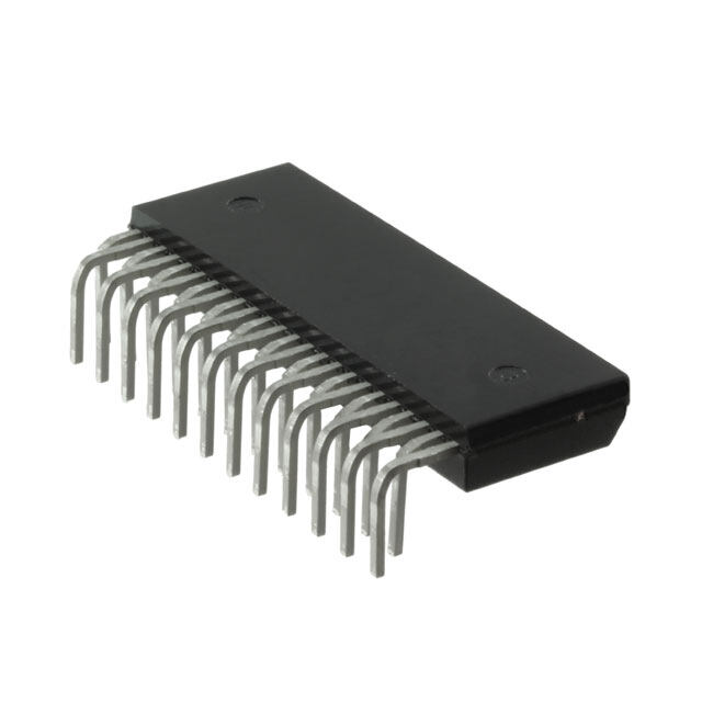
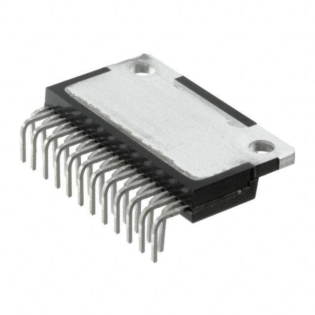
ICGOO电子元器件商城为您提供UC3717ANG4由Texas Instruments设计生产,在icgoo商城现货销售,并且可以通过原厂、代理商等渠道进行代购。 UC3717ANG4价格参考。Texas InstrumentsUC3717ANG4封装/规格:PMIC - 全,半桥驱动器, Half Bridge (2) Driver General Purpose, Stepper Motors Bipolar 16-PDIP。您可以下载UC3717ANG4参考资料、Datasheet数据手册功能说明书,资料中有UC3717ANG4 详细功能的应用电路图电压和使用方法及教程。
| 参数 | 数值 |
| 产品目录 | 集成电路 (IC) |
| 描述 | IC BRIDGE DRIVER PAR 16-DIP |
| 产品分类 | PMIC - 电机, 电桥式驱动器 |
| 品牌 | Texas Instruments |
| 数据手册 | http://www.ti.com/lit/pdf/slus369 |
| 产品图片 |
|
| 产品型号 | UC3717ANG4 |
| rohs | 无铅 / 符合限制有害物质指令(RoHS)规范要求 |
| 产品系列 | - |
| 供应商器件封装 | 16-PDIP |
| 其它名称 | 296-36171-5 |
| 功能 | 功率桥 - 逻辑驱动功率级 |
| 包装 | 管件 |
| 安装类型 | 通孔 |
| 封装/外壳 | 16-DIP(0.300",7.62mm) |
| 工作温度 | 0°C ~ 70°C |
| 应用 | 通用 |
| 接口 | 并联 |
| 标准包装 | 25 |
| 电压-电源 | 4.75 V ~ 5.25 V |
| 电压-负载 | 10 V ~ 46 V |
| 电机类型-AC,DC | - |
| 电机类型-步进 | 双极性 |
| 电流-输出 | 1A |
| 输出配置 | 全 H 桥,(1) 单 |


- 商务部:美国ITC正式对集成电路等产品启动337调查
- 曝三星4nm工艺存在良率问题 高通将骁龙8 Gen1或转产台积电
- 太阳诱电将投资9.5亿元在常州建新厂生产MLCC 预计2023年完工
- 英特尔发布欧洲新工厂建设计划 深化IDM 2.0 战略
- 台积电先进制程称霸业界 有大客户加持明年业绩稳了
- 达到5530亿美元!SIA预计今年全球半导体销售额将创下新高
- 英特尔拟将自动驾驶子公司Mobileye上市 估值或超500亿美元
- 三星加码芯片和SET,合并消费电子和移动部门,撤换高东真等 CEO
- 三星电子宣布重大人事变动 还合并消费电子和移动部门
- 海关总署:前11个月进口集成电路产品价值2.52万亿元 增长14.8%

PDF Datasheet 数据手册内容提取
UC3717A Stepper Motor Drive Circuit FEATURES DESCRIPTION • Full-Step, Half-Step and Micro-Step The UC3717A is an improved version of the UC3717, used to switch Capability drive the current in one winding of a bipolar stepper motor. The UC3717A has been modified to supply higher winding current, more • Bipolar Output Current up to 1A reliable thermal protection, and improved efficiency by providing inte- • Wide Range of Motor Supply Voltage grated bootstrap circuitry to lower recirculation saturation voltages. 10-46V The diagram shown below presents the building blocks of the • Low Saturation Voltage with Integrated UC3717A. Included are an LS-TTL compatible logic input, a current sensor, a monostable, a thermal shutdown network, and an H-bridge Bootstrap output stage. The output stage features built-in fast recovery com- • Built-In Fast Recovery Commutating mutating diodes and integrated bootstrap pull up. Two UC3717As Diodes and a few external components form a complete control and drive • Current Levels Selected in Steps or Varied unit for LS-TTL or micro-processor controlled stepper motor systems. Continuously The UC3717A is characterized for operation over the temperature • Thermal Protection with Soft Intervention range of 0°C to +70°C. ABSOLUTE MAXIMUM RATINGS (Note 1) Voltage Logic Supply, VCC. . . . . . . . . . . . . . . . . . . . . . . . . . . . . . . . . . . . . . 7V Output Supply, Vm. . . . . . . . . . . . . . . . . . . . . . . . . . . . . . . . . . . . . 50V Input Voltage Logic Inputs (Pins 7, 8, 9). . . . . . . . . . . . . . . . . . . . . . . . . . . . . . . . 6V Note 1: All voltages are with respect to ground, Pins 4, Analog Input (Pin 10). . . . . . . . . . . . . . . . . . . . . . . . . . . . . . . . . . . VCC 5, 12, 13. Currents are positive into, negative out of the Reference Input (Pin 11). . . . . . . . . . . . . . . . . . . . . . . . . . . . . . . . 15V specified terminal. Pin numbers refer to DIL-16 pack- age. Input Current Consult Packaging Section of Databook for thermal limi- Logic Inputs (Pins 7, 8, 9). . . . . . . . . . . . . . . . . . . . . . . . . . . . . -10mA tations and considerations of package. Analog Inputs (Pins 10, 11). . . . . . . . . . . . . . . . . . . . . . . . . . . . -10mA Output Current (Pins 1, 15) . . . . . . . . . . . . . . . . . . . . . . . . . . . . . . . – 1.2A Junction Temperature, TJ. . . . . . . . . . . . . . . . . . . . . . . . . . . . . . . +150°C Storage Temperature Range, TS. . . . . . . . . . . . . . . . . . -55°C to +150°C BLOCK DIAGRAM 4/97 1
UC3717A CONNECTION DIAGRAMS PACKAGE PIN FUNCTION DIL-16 (TOP VIEW) PLCC-20 (TOP VIEW) FUNCTION PIN J or N Package Q Package N/C 1 BOUT 2 Timing 3 Vm 4 Gnd 5 N/C 6 Gnd 7 VCC 8 I1 9 Phase 10 N/C 11 I0 12 Current 13 VR 14 Gnd 15 N/C 16 Gnd 17 Vm 18 AOUT 19 Emitters 20 ELECTRICAL CHARACTERISTICS (Refer to the test circuit, Figure 6. Vm = 36V, VCC = 5V, VR = 5V, TA = 0(cid:176) C to 70(cid:176) C, unless otherwise stated, TA = TJ.) PARAMETERS TEST CONDITIONS MIN TYP MAX UNITS Supply Voltage, Vm (Pins 3, 14) 10 46 V Logic Supply Voltage, VCC (Pin 6) 4.75 5.25 V Logic Supply Current, ICC (Pin 6) IO = I1 = 0 7 15 mA Thermal Shutdown Temperature +160 +180 °C Logic Inputs Input Low Voltage, (Pins 7, 8, 9) 0.8 V Input High Voltage, (Pins 7, 8, 9) 2 VCC V Low Voltage Input Current, (Pins 7, 8, 9) VI = 0.4V, Pin 8 -100 m A VI = 0.4V, Pins 7 and 9 -400 mA High Voltage Input Current, (Pins 7, 8, 9) VI = 2.4V 10 m A Comparators Comparator Low, Threshold Voltage (Pin 10) VR = 5V; IO = L; I1 = H 66 80 90 mV Comparator Medium, Threshold Voltage (Pin 10) VR = 5V; IO = H; I1 = L 236 250 266 mV Comparator High, Threshold Voltage (Pin 10) VR = 5V; IO = L; I1 = L 396 420 436 mV Comparator Input, Current (Pin 10) – 20 m A Cutoff Time, tOFF RT = 56kW , CT = 820pF 25 35 m s Turn Off Delay, tD (See Figure 5) 2 m s Source Diode-Transistor Pair Saturation Voltage, VSAT (Pins 1, 15) Im = -0.5A, Conduction Period 1.7 2.1 V (See Figure 5) Im = -0.5A, Recirculation Period 1.1 1.35 V Saturation Voltage, VSAT (Pins 1, 15) Im = -1A, Conduction Period 2.1 2.8 V (See Figure 5) Im = -1A, Recirculation Period 1.7 2.5 V Leakage Current Vm = 40V 300 m A Diode Forward Voltage, VF Im = -0.5A 1 1.25 V Im = -1A 1.3 1.7 V 2
UC3717A ELECTRICAL (Refer to the test circuit, Figure 6. VM = 36V, VCC = 5V, VR = 5V, TA = 0(cid:176) C to 70(cid:176) C, unless CHARACTERISTICS (cont.) otherwise stated, TA = TJ.) PARAMETERS TEST CONDITIONS MIN TYP MAX UNITS Sink Diode-Transistor Pair Saturation Voltage, VSAT (Pins 1, 15) Im = 0.5A 0.8 1.1 1.35 V Im = 1A 1.6 2.3 V Leakage Current Vm = 40V 300 m A Diode Forward Voltage, VF Im = 0.5A 1.1 1.5 V Im = 1A 1.4 2 V Figure 1. Typical Source Saturation Voltage Figure 2. Typical Source Saturation Voltage vs Output Current (Recirculation Period) vs Output Current (Conduction Period) Figure 3. Typical Sink Saturation Voltage vs Output Current Figure 5. Typical Waveforms with MA Regulating (phase = 0) Figure 4. Typical Power Dissipation vs Output Current 3
UC3717A Figure 6. UC3717A Test Circuit FUNCTIONAL DESCRIPTION The UC3717A’s drive circuit shown in the block diagram saturation voltage of source transistor Q2 during recircu- includes the following components. lation, thus improving efficiency by reducing power dissi- (1) H-bridge output stage pation. (2) Phase polarity logic (3) Voltage divider coupled with current sensing compa- rators (4) Two-bit D/A current level select (5) Monostable generating fixed off-time (6) Thermal protection OUTPUT STAGE The UC3717A’s output stage consists of four Darlington power transistors and associated recirculating power di- odes in a full H-bridge configuration as shown in Figure 7. Also presented, is the new added feature of inte- grated bootstrap pull up, which improves device per- formance during switched mode operation. While in switched mode, with a low level phase polarity input, Q2 is on and Q3 is being switched. At the moment Q3 turns off, winding current begins to decay through the commu- tating diode pulling the collector of Q3 above the supply Note: Dashed lines indicate current decay paths. voltage. Meanwhile, Q6 turns on pulling the base of Q2 Figure 7. Simplified Schematic of Output Stage higher than its previous value. The net effect lowers the 4
UC3717A FUNCTIONAL DESCRIPTION (cont.) PHASE POLARITY INPUT ture to a maximum of 180C by reducing the winding cur- The UC3717A phase polarity input controls current direc- rent. tion in the motor winding. Built-in hysteresis insures im- PERFORMANCE CONSIDERATIONS munity to noise, something frequently present in In order to achieve optimum performance from the switched drive environments. A low level phase polarity UC3717A careful attention should be given to the follow- input enables Q2 and Q3 as shown in Figure 7. During ing items. phase reversal, the active transistors are both turned off while winding current delays through the commutating di- External Components: The UC3717A requires a mini- odes shown. As winding current decays to zero, the inac- mal number of external components to form a complete tive transistors Q1 and Q4 turn on and charge the control and switch drive unit. However, proper selection winding with current of the reverse direction. This delay of external components is necessary for optimum per- insures noise immunity and freedom from power supply formance. The timing pin, (pin 2) is normally connected current spikes caused by overlapping drive signals. to an RC network which sets the off-time for the sink power transistor during switched mode. As shown in Fig- PHASE INPUT Q1, Q4 Q2, Q3 ure 8, prior to switched mode, the winding current in- LOW OFF ON creases exponentially to a peak value. Once peak HIGH ON OFF current is attained the monostable is triggered which turns off the lower sink drivers for a fixed off-time. During CURRENT CONTROL off-time winding current decays through the appropriate The voltage divider, comparators, monostable, and two- diode and source transistor. The moment off-time times bit D/A provide a means to sense winding peak current, out, the motor current again rises exponentially produc- select winding peak current, and disable the winding sink ing the ripple waveform shown. The magnitude of wind- transistors. ing ripple is a direct function of off-time. For a given The UC3717A switched driver accomplishes current con- off-time TOFF, the values of RT and CT can be calculated trol using an algorithm referred to as "fixed off-time." from the expression: When a voltage is applied across the motor winding, the TOFF = 0.69RTCT current through the winding increases exponentially. The with the restriction that RT should be in the range of 10- current can be sensed across an external resistor as an 100k. As shown in Figure 5, the switch frequency FS is a analog voltage proportional to instantaneous current. function of TOFF and TON. Since TON is a function of the This voltage is normally filtered with a simple RC low- reference voltage, sense resistor, motor supply, and pass network to remove high frequency transients, and winding electrical characteristics, it generally varies dur- then compared to one of the three selectable thresholds. ing different modes of operation. Thus, FS may be ap- The two bit D/A input signal determines which one of the proximated nominally as: three thresholds is selected, corresponding to a desired FS = 1⁄1.5 (TOFF). winding peak current level. At the moment the sense volt- Normally, Switch Frequency Is Selected Greater than age rises above the selected threshold, the UC3717A’s monostable is triggered and disables both output sink drivers for a fixed off-time. The winding current then cir- culates through the source transistor and appropriate di- ode. The reference terminal of the UC3717A provides a means of continuously adjusting the current threshold to allow microstepping. Table 1 presents the relationship between the two-bit D/A input signal and selectable cur- rent level. TABLE 1 IO I1 CURRENT LEVEL 0 0 100% 1 0 60% Figure 8. A typical winding current waveform. Wind- 0 1 19% ing current rises exponentially to a selected peak 1 1 Current Inhibit value. The peak value is limited by switched mode operation producing a ripple in winding current. A OVERLOAD PROTECTION phase polarity reversal command is given and wind- The UC3717A is equipped with a new, more reliable ther- ing current decays to zero, then increases exponen- mal shutdown circuit which limits the junction tempera- tially. 5
UC3717A FUNCTIONAL DESCRIPTION (cont.) Low-pass filter components RC CC should be selected so current is excessive and must be prevented. This is ac- that all switching transients from the power transistors complished with switch drive by repetitively switching the and commutating diodes are well smoothed, but the pri- sink drivers on and off, so as to maintain an average mary signal, which can be in the range of 1/TOFF or value of current equal to the rated value. This results in a higher must be passed. Figure 5A shows the waveform small amount of ripple in the controlled current, but the which must be smoothed, Figure 5B presents the desired increase in step rate and performance may be consider- waveform that just smoothes out overshoot without radi- able. cal distortion. Interference: Electrical noise generated by the chopping The sense resistor should be chosen as small as practi- action can cause interference problems, particularly in cal to allow as much of the winding supply voltage to be the vicinity of magnetic storage media. With this in mind, used as overdrive to the motor winding. VRS, the voltage printed circuit layouts, wire runs and decoupling must be across the sense resistor, should not exceed 1.5V. considered. 0.01 to 0.1m F ceramic capacitors for high fre- Voltage Overdrive: In many applications, maximum quency bypass located near the drive package across speed or step rate is a desirable performance charac- V+ and ground might be very helpful. The connection teristic. Maximum step rate is a direct function of the time and ground leads of the current sensing components necessary to reverse winding current with each step. In should be kept as short as possible. response to a constant motor supply voltage, the winding Half-Stepping: In half step sequence the power input to current changes exponentially with time, whose shape is the motor alternates between one or two phases being determined by the winding time constant and expressed energized. In a two phase motor the electrical phase shift as: between the windings is 90°. The torque developed is the Im = R [1- EXVPm (- RT⁄L)] vwehceton ro nsluym o noef wthined intwgo is weinnedrignigzse de tnheer tgoizrqeude. oTfh tehree fmoroe- as presented in Figure 9. With rated voltage applied, the tor is reduced by approximately 30%. This causes a time required to reach rated current is excessive when torque ripple and if it is necessary to compensate for this, compared with the time required with over-voltage ap- the VR input can be used to boost the current of the sin- plied, even though the time constant L/R remains con- gle energized winding. stant. With over-voltage however, the final value of Figure 9. With rated voltage applied, winding current does not exceed rated value, but takes L/R seconds to reach 63% of its final value - probably too long. Increased performance requires an increase in applied volt- age, of overdrive, and therefore a means to limit current. The UC3717A motor driver performs this task effi- ciently. 6
UC3717A MOUNTING INSTRUCTIONS The q JA of the UC3717AN plastic package can be re- 12. The input can be controlled by a microprocessor, duced by soldering the GND pins to a suitable copper TTL, LS, or CMOS logic. area of the printed circuit board or to an external heat The timing diagram in Figure 13 shows the required sig- sink. Due to different lead frame design, q JA of the ce- nal input for a two phase, full step stepping sequence. ramic J package cannot be similarly reduced. Figure 14 shows the required input signal for a one The diagram of Figure 11 shows the maximum package phase-two phase stepping sequence called half-step- power PTOT and the q JA as a function of the side " l " of ping. two equal square copper areas having a thickness of 35m The circuit of Figure 15 provides the signal shown in Fig- (see Figure 10). ure 13, and in conjunction with the circuit shown in Fig- ure 12 will implement a pulse-to-step two phase, full step, bi-directional motor drive. Figure 10. Example of P.C. Board Copper Area which is used as Heatsink. During soldering the pins’ temperature must not exceed 260°C and the soldering time must not be longer than 12 seconds. The printed circuit copper area must be connected to electrical ground. Figure 12. Typical Chopper Drive for a Two Phase Permanent Magnet Motor. The schematic of Figure 16 shows a pulse to half step circuit generating the signal shown in Figure 14. Care Figure 11. Maximum Package Power and Junction to Ambient Thermal Resistance vs Side "l". has been taken to change the phase signal the same time the current inhibit is applied. This will allow the cur- APPLICATIONS rent to decay faster and therefore enhance the motor A typical chopper drive for a two phase bipolar perma- performance at high step rates. nent magnet or hybrid stepping motor is shown in Figure 7
UC3717A Figure 13. Phase Input Signal for Two Phase Full Step Drive (4 Step Sequence) Figure 14. Phase and Current-Inhibit Signal for Half-Stepping (8 Step Sequence) Figure 15. Full Step, Bi-directional Two Phase Drive Logic Figure 16. Half-Step, Bi-directional Drive Logic UNITRODE CORPORATION 7 CONTINENTAL BLVD. • MERRIMACK, NH 03054 TEL. (603) 424-2410 • FAX (603) 424-3460 8
PACKAGE OPTION ADDENDUM www.ti.com 6-May-2009 PACKAGING INFORMATION OrderableDevice Status(1) Package Package Pins Package EcoPlan(2) Lead/BallFinish MSLPeakTemp(3) Type Drawing Qty UC3717AN ACTIVE PDIP N 16 25 Green(RoHS& CUNIPDAU N/AforPkgType noSb/Br) UC3717ANG4 ACTIVE PDIP N 16 25 Green(RoHS& CUNIPDAU N/AforPkgType noSb/Br) UC3717AQ ACTIVE PLCC FN 20 46 Green(RoHS& CUSN Level-2-260C-1YEAR noSb/Br) UC3717AQG3 ACTIVE PLCC FN 20 46 Green(RoHS& CUSN Level-2-260C-1YEAR noSb/Br) UC3717AQTR ACTIVE PLCC FN 20 1000 Green(RoHS& CUSN Level-2-260C-1YEAR noSb/Br) UC3717AQTRG3 ACTIVE PLCC FN 20 1000 Green(RoHS& CUSN Level-2-260C-1YEAR noSb/Br) (1)Themarketingstatusvaluesaredefinedasfollows: ACTIVE:Productdevicerecommendedfornewdesigns. LIFEBUY:TIhasannouncedthatthedevicewillbediscontinued,andalifetime-buyperiodisineffect. NRND:Notrecommendedfornewdesigns.Deviceisinproductiontosupportexistingcustomers,butTIdoesnotrecommendusingthispartin anewdesign. PREVIEW:Devicehasbeenannouncedbutisnotinproduction.Samplesmayormaynotbeavailable. OBSOLETE:TIhasdiscontinuedtheproductionofthedevice. (2)EcoPlan-Theplannedeco-friendlyclassification:Pb-Free(RoHS),Pb-Free(RoHSExempt),orGreen(RoHS&noSb/Br)-pleasecheck http://www.ti.com/productcontentforthelatestavailabilityinformationandadditionalproductcontentdetails. TBD:ThePb-Free/Greenconversionplanhasnotbeendefined. Pb-Free(RoHS):TI'sterms"Lead-Free"or"Pb-Free"meansemiconductorproductsthatarecompatiblewiththecurrentRoHSrequirements forall6substances,includingtherequirementthatleadnotexceed0.1%byweightinhomogeneousmaterials.Wheredesignedtobesoldered athightemperatures,TIPb-Freeproductsaresuitableforuseinspecifiedlead-freeprocesses. Pb-Free(RoHSExempt):ThiscomponenthasaRoHSexemptionforeither1)lead-basedflip-chipsolderbumpsusedbetweenthedieand package, or 2) lead-based die adhesive used between the die and leadframe. The component is otherwise considered Pb-Free (RoHS compatible)asdefinedabove. Green(RoHS&noSb/Br):TIdefines"Green"tomeanPb-Free(RoHScompatible),andfreeofBromine(Br)andAntimony(Sb)basedflame retardants(BrorSbdonotexceed0.1%byweightinhomogeneousmaterial) (3) MSL, Peak Temp. -- The Moisture Sensitivity Level rating according to the JEDEC industry standard classifications, and peak solder temperature. Important Information and Disclaimer:The information provided on this page represents TI's knowledge and belief as of the date that it is provided. TI bases its knowledge and belief on information provided by third parties, and makes no representation or warranty as to the accuracy of such information. Efforts are underway to better integrate information from third parties. TI has taken and continues to take reasonable steps to provide representative and accurate information but may not have conducted destructive testing or chemical analysis on incomingmaterialsandchemicals.TIandTIsuppliersconsidercertaininformationtobeproprietary,andthusCASnumbersandotherlimited informationmaynotbeavailableforrelease. InnoeventshallTI'sliabilityarisingoutofsuchinformationexceedthetotalpurchasepriceoftheTIpart(s)atissueinthisdocumentsoldbyTI toCustomeronanannualbasis. Addendum-Page1
PACKAGE MATERIALS INFORMATION www.ti.com 6-Oct-2008 TAPE AND REEL INFORMATION *Alldimensionsarenominal Device Package Package Pins SPQ Reel Reel A0(mm) B0(mm) K0(mm) P1 W Pin1 Type Drawing Diameter Width (mm) (mm) Quadrant (mm) W1(mm) UC3717AQTR PLCC FN 20 1000 330.0 16.4 10.3 10.3 4.9 12.0 16.0 Q1 PackMaterials-Page1
PACKAGE MATERIALS INFORMATION www.ti.com 6-Oct-2008 *Alldimensionsarenominal Device PackageType PackageDrawing Pins SPQ Length(mm) Width(mm) Height(mm) UC3717AQTR PLCC FN 20 1000 346.0 346.0 33.0 PackMaterials-Page2
IMPORTANTNOTICE TexasInstrumentsIncorporatedanditssubsidiaries(TI)reservetherighttomakecorrections,modifications,enhancements,improvements, andotherchangestoitsproductsandservicesatanytimeandtodiscontinueanyproductorservicewithoutnotice.Customersshould obtainthelatestrelevantinformationbeforeplacingordersandshouldverifythatsuchinformationiscurrentandcomplete.Allproductsare soldsubjecttoTI’stermsandconditionsofsalesuppliedatthetimeoforderacknowledgment. TIwarrantsperformanceofitshardwareproductstothespecificationsapplicableatthetimeofsaleinaccordancewithTI’sstandard warranty.TestingandotherqualitycontroltechniquesareusedtotheextentTIdeemsnecessarytosupportthiswarranty.Exceptwhere mandatedbygovernmentrequirements,testingofallparametersofeachproductisnotnecessarilyperformed. TIassumesnoliabilityforapplicationsassistanceorcustomerproductdesign.Customersareresponsiblefortheirproductsand applicationsusingTIcomponents.Tominimizetherisksassociatedwithcustomerproductsandapplications,customersshouldprovide adequatedesignandoperatingsafeguards. TIdoesnotwarrantorrepresentthatanylicense,eitherexpressorimplied,isgrantedunderanyTIpatentright,copyright,maskworkright, orotherTIintellectualpropertyrightrelatingtoanycombination,machine,orprocessinwhichTIproductsorservicesareused.Information publishedbyTIregardingthird-partyproductsorservicesdoesnotconstitutealicensefromTItousesuchproductsorservicesora warrantyorendorsementthereof.Useofsuchinformationmayrequirealicensefromathirdpartyunderthepatentsorotherintellectual propertyofthethirdparty,oralicensefromTIunderthepatentsorotherintellectualpropertyofTI. ReproductionofTIinformationinTIdatabooksordatasheetsispermissibleonlyifreproductioniswithoutalterationandisaccompanied byallassociatedwarranties,conditions,limitations,andnotices.Reproductionofthisinformationwithalterationisanunfairanddeceptive businesspractice.TIisnotresponsibleorliableforsuchaltereddocumentation.Informationofthirdpartiesmaybesubjecttoadditional restrictions. ResaleofTIproductsorserviceswithstatementsdifferentfromorbeyondtheparametersstatedbyTIforthatproductorservicevoidsall expressandanyimpliedwarrantiesfortheassociatedTIproductorserviceandisanunfairanddeceptivebusinesspractice.TIisnot responsibleorliableforanysuchstatements. TIproductsarenotauthorizedforuseinsafety-criticalapplications(suchaslifesupport)whereafailureoftheTIproductwouldreasonably beexpectedtocauseseverepersonalinjuryordeath,unlessofficersofthepartieshaveexecutedanagreementspecificallygoverning suchuse.Buyersrepresentthattheyhaveallnecessaryexpertiseinthesafetyandregulatoryramificationsoftheirapplications,and acknowledgeandagreethattheyaresolelyresponsibleforalllegal,regulatoryandsafety-relatedrequirementsconcerningtheirproducts andanyuseofTIproductsinsuchsafety-criticalapplications,notwithstandinganyapplications-relatedinformationorsupportthatmaybe providedbyTI.Further,BuyersmustfullyindemnifyTIanditsrepresentativesagainstanydamagesarisingoutoftheuseofTIproductsin suchsafety-criticalapplications. TIproductsareneitherdesignednorintendedforuseinmilitary/aerospaceapplicationsorenvironmentsunlesstheTIproductsare specificallydesignatedbyTIasmilitary-gradeor"enhancedplastic."OnlyproductsdesignatedbyTIasmilitary-grademeetmilitary specifications.BuyersacknowledgeandagreethatanysuchuseofTIproductswhichTIhasnotdesignatedasmilitary-gradeissolelyat theBuyer'srisk,andthattheyaresolelyresponsibleforcompliancewithalllegalandregulatoryrequirementsinconnectionwithsuchuse. TIproductsareneitherdesignednorintendedforuseinautomotiveapplicationsorenvironmentsunlessthespecificTIproductsare designatedbyTIascompliantwithISO/TS16949requirements.Buyersacknowledgeandagreethat,iftheyuseanynon-designated productsinautomotiveapplications,TIwillnotberesponsibleforanyfailuretomeetsuchrequirements. FollowingareURLswhereyoucanobtaininformationonotherTexasInstrumentsproductsandapplicationsolutions: Products Applications Amplifiers amplifier.ti.com Audio www.ti.com/audio DataConverters dataconverter.ti.com Automotive www.ti.com/automotive DLP®Products www.dlp.com Broadband www.ti.com/broadband DSP dsp.ti.com DigitalControl www.ti.com/digitalcontrol ClocksandTimers www.ti.com/clocks Medical www.ti.com/medical Interface interface.ti.com Military www.ti.com/military Logic logic.ti.com OpticalNetworking www.ti.com/opticalnetwork PowerMgmt power.ti.com Security www.ti.com/security Microcontrollers microcontroller.ti.com Telephony www.ti.com/telephony RFID www.ti-rfid.com Video&Imaging www.ti.com/video RF/IFandZigBee®Solutions www.ti.com/lprf Wireless www.ti.com/wireless MailingAddress:TexasInstruments,PostOfficeBox655303,Dallas,Texas75265 Copyright©2009,TexasInstrumentsIncorporated