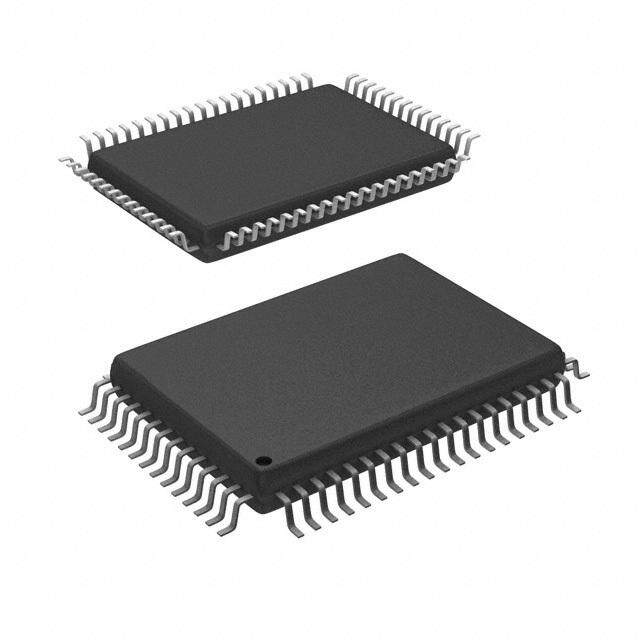
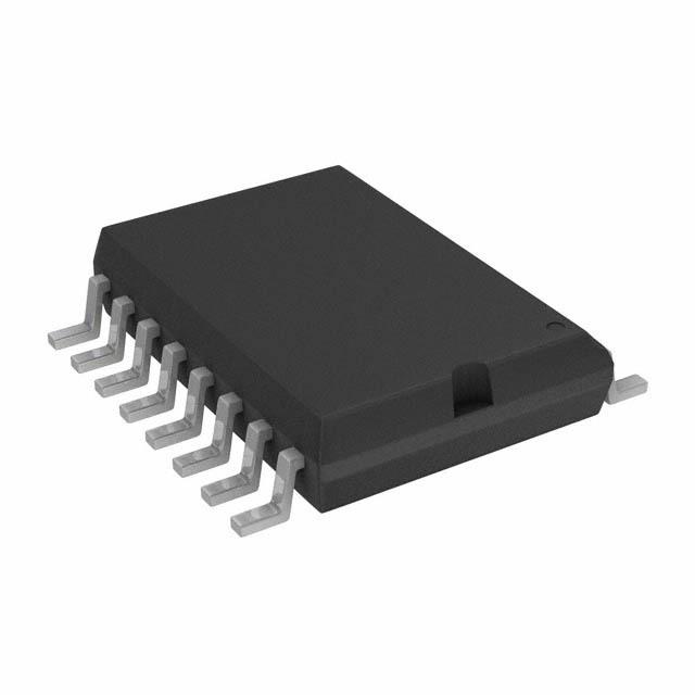
ICGOO在线商城 > 集成电路(IC) > PMIC - 栅极驱动器 > UC2715N
- 型号: UC2715N
- 制造商: Texas Instruments
- 库位|库存: xxxx|xxxx
- 要求:
| 数量阶梯 | 香港交货 | 国内含税 |
| +xxxx | $xxxx | ¥xxxx |
查看当月历史价格
查看今年历史价格
UC2715N产品简介:
ICGOO电子元器件商城为您提供UC2715N由Texas Instruments设计生产,在icgoo商城现货销售,并且可以通过原厂、代理商等渠道进行代购。 UC2715N价格参考。Texas InstrumentsUC2715N封装/规格:PMIC - 栅极驱动器, Low-Side Gate Driver IC Non-Inverting 8-PDIP。您可以下载UC2715N参考资料、Datasheet数据手册功能说明书,资料中有UC2715N 详细功能的应用电路图电压和使用方法及教程。
| 参数 | 数值 |
| 产品目录 | 集成电路 (IC)半导体 |
| 描述 | IC COMPLEMENT SW FET DRVR 8-DIP门驱动器 Complementary Switch FET Drivers |
| 产品分类 | PMIC - MOSFET,电桥驱动器 - 外部开关集成电路 - IC |
| 品牌 | Texas Instruments |
| 产品手册 | |
| 产品图片 |
|
| rohs | 符合RoHS无铅 / 符合限制有害物质指令(RoHS)规范要求 |
| 产品系列 | 电源管理 IC,门驱动器,Texas Instruments UC2715N- |
| 数据手册 | |
| 产品型号 | UC2715N |
| 上升时间 | 30 ns |
| 下降时间 | 25 ns |
| 产品 | Driver ICs - Various |
| 产品目录页面 | |
| 产品种类 | 门驱动器 |
| 供应商器件封装 | 8-PDIP |
| 其它名称 | 296-11667-5 |
| 包装 | 管件 |
| 单位重量 | 528.600 mg |
| 商标 | Texas Instruments |
| 安装类型 | 通孔 |
| 安装风格 | Through Hole |
| 封装 | Tube |
| 封装/外壳 | 8-DIP(0.300",7.62mm) |
| 封装/箱体 | PDIP-8 |
| 工作温度 | -40°C ~ 85°C |
| 工厂包装数量 | 50 |
| 延迟时间 | 50ns |
| 最大工作温度 | + 85 C |
| 最小工作温度 | - 40 C |
| 标准包装 | 50 |
| 激励器数量 | 2 Driver |
| 电压-电源 | 7 V ~ 20 V |
| 电流-峰值 | 2A |
| 电源电压-最大 | 20 V |
| 电源电压-最小 | 7 V |
| 电源电流 | 24 mA |
| 类型 | Inverting, Non-Inverting |
| 系列 | UC2715 |
| 输入类型 | PWM |
| 输出数 | 2 |
| 输出电流 | 2 A |
| 输出端数量 | 2 |
| 配置 | 低端 |
| 配置数 | 2 |
| 高压侧电压-最大值(自举) | - |


- 商务部:美国ITC正式对集成电路等产品启动337调查
- 曝三星4nm工艺存在良率问题 高通将骁龙8 Gen1或转产台积电
- 太阳诱电将投资9.5亿元在常州建新厂生产MLCC 预计2023年完工
- 英特尔发布欧洲新工厂建设计划 深化IDM 2.0 战略
- 台积电先进制程称霸业界 有大客户加持明年业绩稳了
- 达到5530亿美元!SIA预计今年全球半导体销售额将创下新高
- 英特尔拟将自动驾驶子公司Mobileye上市 估值或超500亿美元
- 三星加码芯片和SET,合并消费电子和移动部门,撤换高东真等 CEO
- 三星电子宣布重大人事变动 还合并消费电子和移动部门
- 海关总署:前11个月进口集成电路产品价值2.52万亿元 增长14.8%


PDF Datasheet 数据手册内容提取
UC1714, UC1715, UC2714 UC2715, UC3714, UC3715 www.ti.com SLUS170B –FEBRUARY1999–REVISEDMAY2013 Complementary Switch FET Drivers CheckforSamples:UC1714,UC1715,UC2714,UC2715,UC3714,UC3715 FEATURES DESCRIPTION 1 • SingleInput(PWMandTTLCompatible) These two families of high speed drivers are designed to provide drive waveforms for • High-CurrentPowerFETDriver,1-ASource complementary switches. Complementary switch and2-ASink configurations are commonly used in synchronous • AuxiliaryOutputFETDriver,0.5-ASourceand rectification circuits and active clamp/reset circuits, 1-ASink which provide zero voltage switching. In order to facilitate the soft switching transitions, independently • TimeDelaysBetweenPowerandAuxiliary programmable delays between the two output OutputsIndependentlyProgrammablefrom50 waveforms are provided on these drivers. The delay to500-ns pins also have true-zero voltage-sensing capability • TimeDelayorTrueZero-VoltageOperation which allows immediate activation of the IndependentlyConfigurableforEachOutput corresponding switch when zero voltage is applied. • SwitchingFrequencyto1MHz These devices require a PWM-type input to operate and interface with commonly available PWM • Typical50-nsPropagationDelays controllers. • ENBLPinActivates220-μASleepMode In the UC1714 series, the AUX output is inverted to • PowerOutputisActive-LowinSleepMode allow driving a p-channel MOSFET. In the UC1715 • SynchronousRectifierDriver series, the two outputs are configured in a true complementaryfashion. BLOCKDIAGRAM 50ns –500ns 2 PWR TIMER INPUT 6 S Q T1 7 R UC1714 VREF ONLY 50ns –500ns 4 AUX TIMER S 1 VCC Q VCC 5V LOGIC T2 5 R BIAS GATES VREF ENBL 3V TIMER REF GND 3 GND 1.4V ENBL 8 ENABLE PinnumbersrefertoJ,NandDpackages. 1 Pleasebeawarethatanimportantnoticeconcerningavailability,standardwarranty,anduseincriticalapplicationsof TexasInstrumentssemiconductorproductsanddisclaimerstheretoappearsattheendofthisdatasheet. UNLESS OTHERWISE NOTED this document contains Copyright©1999–2013,TexasInstrumentsIncorporated PRODUCTION DATA information current as of publication date. Products conform to specifications per the terms of Texas Instruments standard warranty. Production processing does not necessarilyincludetestingofallparameters.
UC1714, UC1715, UC2714 UC2715, UC3714, UC3715 SLUS170B –FEBRUARY1999–REVISEDMAY2013 www.ti.com ABSOLUTE MAXIMUM RATINGS(1)(2) MIN MAX UNIT AuxiliaryDriverIOH continuous –100 mA peak –500 mA AuxiliaryDriverIOL continuous 200 mA peak 1 A InputVoltageRange(INPUT,ENBL) –0.3 20 V PowerDriverIOH continuous –200 mA peak –1 A PowerDriverIOL continuous 400 mA peak 2 A V Supplyvoltage 20 V CC LeadTemperature(Soldering10seconds) 300 °C OperatingJunctionTemperature(3) 150 °C StorageTemperatureRange –65 150 °C (1) ConsultthePackagingSectionattheendofthisdatasheetforthermallimitationsandspecificationsofpackages. (2) Stressesbeyondthoselistedunderabsolutemaximumratingsmaycausepermanentdamagetothedevice.Thesearestressratings only,andfunctionaloperationofthedeviceattheseoranyotherconditionsbeyondthoseindicatedunderrecommendedoperating conditionsisnotimplied.Exposuretoabsolute-maximum-ratedconditionsforextendedperiodsmayaffectdevicereliability. (3) Unlessotherwiseindicated,voltagesarereferencedtogroundandcurrentsarepositiveinto,negativeoutof,thespecifiedterminals. ELECTRICAL CHARACTERISTICS Unlessotherwisestated,V =15V,ENBL≥2V,R 1=100kΩfromT1toGND,R 2=100kΩfromT2toGND,and−55°C CC T T <T <125°CfortheUC1714andUC1715,–40°C<T <85°CfortheUC2714andUC2715,and0°C<T <70°Cforthe A A A UC3714andUC3715,T =T A J PARAMETER TESTCONDITIONS MIN TYP MAX UNIT Overall V 7 20 V CC I Nominal ENBL=2V 18 24 mA CC Sleepmode ENBL=0.8V 200 300 µA PowerDriver(PWR) Preturn-onPWRoutput,low V =0V,I =10mA,ENBLat 0.3 1.6 V CC OUT 0.8V V PWRoutputlow,sat. INPUT=0.8V,I =40mA 0.3 0.8 PWR OUT V INPUT=0.8V,I =400mA 2.1 2.8 OUT V − PWRoutputhigh,sat. INPUT=2V,I =−20mA 2.1 3 CC OUT V V PWR INPUT=2V,I =−200mA 2.3 3 OUT Risetime C =2200pF 30 60 ns L Falltime C =2200pF 25 60 ns L T1Delay,AUXtoPWR INPUTrisingedge,R 1=10kΩ(1) 20 35 80 T ns INPUTrisingedge,R 1=100kΩ(1) 350 500 700 T PWRPropDelay INPUTfallingedge,50%(2) 35 100 ns AuxiliaryDriver(AUX) V AUXoutputlow,sat. V =2V,I =20mA 0.3 0.8 AUX IN OUT V V =2V,I =200mA 1.8 2.6 IN OUT V – AUXoutputhigh,sat. V =0.8V,I =–10mA 2.1 3 CC IN OUT V V AUX V =0.8V,I =–100mA 2.3 3 IN OUT RiseTime C =1000pF 45 60 ns L (1) T1delayisdefinedfromthe50%pointofthetransitionedgeofAUXtothe10%oftherisingedgeofPWR.T2delayisdefinedfromthe 90%ofthefallingedgeofPWRtothe50%pointofthetransitionedgeofAUX. (2) Propagationdelaytimesaremeasuredfromthe50%pointoftheinputsignaltothe10%pointoftheoutputsignal’stransitionwithno loadonoutputs. 2 SubmitDocumentationFeedback Copyright©1999–2013,TexasInstrumentsIncorporated ProductFolderLinks:UC1714 UC1715 UC2714UC2715 UC3714 UC3715
UC1714, UC1715, UC2714 UC2715, UC3714, UC3715 www.ti.com SLUS170B –FEBRUARY1999–REVISEDMAY2013 ELECTRICAL CHARACTERISTICS (continued) Unlessotherwisestated,V =15V,ENBL≥2V,R 1=100kΩfromT1toGND,R 2=100kΩfromT2toGND,and−55°C CC T T <T <125°CfortheUC1714andUC1715,–40°C<T <85°CfortheUC2714andUC2715,and0°C<T <70°Cforthe A A A UC3714andUC3715,T =T A J PARAMETER TESTCONDITIONS MIN TYP MAX UNIT FallTime C =1000pF 30 60 ns L T2Delay,PWRtoAUX INPUTfallingedge,R 2=10kΩ(1) 20 50 80 T ns INPUTfallingedge,R 2=100kΩ(1) 250 350 550 T AUXPropDelay INPUTrisingedge,50%(2) 35 80 ns Enable(ENBL) InputThreshold 0.8 1.2 2 V I InputCurrent ENBL=15V 1 10 µA IH I InputCurrent ENBL=0V –1 –10 µA IL T1 CurrentLimit T1=0V –1.6 –2 mA NominalVoltageatT1 2.7 3 3.3 V MinimumT1Delay T1=2.5V(1) 40 70 ns T2 CurrentLimit T2=0V –1.2 –2 mA NominalVoltageatT2 2.7 3 3.3 V MinumumT2Delay T2=2.5V(1) 50 100 ns Input(INPUT) InputThreshold 0.8 1.4 2 V I InputCurrent INPUT=15V 1 10 µA IH I InputCurrent INPUT=0V –5 –20 µA IL DEVICE INFORMATION DIL-8,SOIC-8;JorN,DPackages (TOPVIEW) SOIC-16;DPPackage (TOPVIEW) Copyright©1999–2013,TexasInstrumentsIncorporated SubmitDocumentationFeedback 3 ProductFolderLinks:UC1714 UC1715 UC2714UC2715 UC3714 UC3715
UC1714, UC1715, UC2714 UC2715, UC3714, UC3715 SLUS170B –FEBRUARY1999–REVISEDMAY2013 www.ti.com PIN DESCRIPTIONS AUX TheAUXswitchesimmediatelyattherisingedgeofINPUT’butwaitsthroughtheT2delayafterthefalling edgeofINPUTbeforeswitching.AUXiscapableofsourcing0.5Aandsinking1Aofdrivecurrent.See theTimeRelationshipsdiagrambelow(Figure1)forthedifferencesbetweentheUC1714andUC1715for INPUT,MAIN,andAUX.Duringsleepmode,AUXisinactivewithahighimpedance. ENBL TheENBLinputswitchesatTTLlogiclevels(approximately1.2V),andtheinputrangeisfrom0to20V. TheENBLinputplacesthedeviceintosleepmodewhenitisalogicallow.ThecurrentintoVCCduring thesleepmodeistypically220μA. GND Thisisthereferencepinforallinputvoltagesandthereturnpointforalldevicecurrents.GNDcarriesthe fullpeaksinkingcurrentfromtheoutputs.AnytendencyfortheoutputstoringbelowGNDvoltagemust bedampedorclampedsuchthatGNDremainsthemostnegativepotential. INPUT TheinputswitchesatTTLlogiclevels(approximately1.4V)buttheallowablerangeisfrom0to20V, allowingdirectconnectiontomostcommonICPWMcontrolleroutputs.Therisingedgeimmediately switchestheAUXoutput,andinitiatesatimingdelay,T1,beforeswitchingonthePWRoutput.Similarly, theINPUTfallingedgeimmediatelyturnsoffthePWRoutputandinitiatesatimingdelay,T2,before switchingtheAUXoutput. NotethatiftheinputsignalcomesfromacontrollerwithFETdrivecapability,thissignalprovidesanother option.INPUTandPWRprovideadelayonlyattheleadingedgewhileINPUTandAUXprovidethedelay atthetrailingedge. PWR ThePWRoutputwaitsfortheT1delayaftertherisingedgeofINPUTbeforeswitchingon,butswitches offimmediatelyatthefallingedgeofINPUT’(neglectingpropagationdelays).Thisoutputiscapableof sourcing1Aandsinking2Aofpeakgate-drivecurrent.PWRoutputincludesapassive,self-biasedcircuit whichholdsthispinactivelow,whenENBL≤ 0.8VregardlessofthevoltageofVCC. T1 AresistortogroundprogramsthetimedelaybetweentheAUXswitchturnoffandPWRturnon. T2 ThispinfunctionsinthesamewayasT1butcontrolsthetimedelaybetweenPWRturnoffandactivation oftheAUXswitch. T1,T2 Theresistoroneachofthesepinssetsthechargingcurrentoninternaltimingcapacitorstoprovide independenttimecontrol.Thenominalvoltagelevelateachpinis3Vandthecurrentisinternallylimited to1mA.ThetotaldelayfromINPUTtoeachoutputincludesapropagationdelayinadditiontothe programmabletimerbutbecausethepropagationdelaysareapproximatelyequal,therelativetimedelay betweenthetwooutputscanbeassumedtobesolelyafunctionoftheprogrammeddelays.The relationshipofthetimedelayvs.RTisshownintheTYPICALCHARACTERISTICScurves(seeFigure2). Eitherorbothpinsarealternativelyusedforvoltagesensinginlieuofdelayprogramming,whichisdone bypullingthetimerpinsbelowtheirnominalvoltagelevelwhichimmediatelyactivatesthetimeroutput. VCC TheV inputrangeisfrom7to20V.ThispinmustbebypassedwithacapacitortoGNDconsistentwith CC peakloadcurrentdemands. 4 SubmitDocumentationFeedback Copyright©1999–2013,TexasInstrumentsIncorporated ProductFolderLinks:UC1714 UC1715 UC2714UC2715 UC3714 UC3715
UC1714, UC1715, UC2714 UC2715, UC3714, UC3715 www.ti.com SLUS170B –FEBRUARY1999–REVISEDMAY2013 TYPICAL CHARACTERISTICS T1DELAY,T2DELAY vs TIMERELATIONSHIPS R T INPUT PROPAGATION DELAYS PWR OUTPUT T1 DELAY T2 DELAY UC1714 AUX OUTPUT UC1715 AUX OUTPUT (2)T1delayisdefinedfromthe50%pointofthetransitionedgeof AUXtothe10%oftherisingedgeofPWR.T2delayisdefinedfrom the90%ofthefallingedgeofPWRtothe50%pointofthetransition edgeofAUX. Figure1. Figure2. I CC vs I CC SWITCHINGFREQUENCYWITHNOLOADAND50% vs DUTYCYCLER 1=R 2=50k R WITHOPPOSITER =50k T T T T Figure3. Figure4. Copyright©1999–2013,TexasInstrumentsIncorporated SubmitDocumentationFeedback 5 ProductFolderLinks:UC1714 UC1715 UC2714UC2715 UC3714 UC3715
UC1714, UC1715, UC2714 UC2715, UC3714, UC3715 SLUS170B –FEBRUARY1999–REVISEDMAY2013 www.ti.com TYPICAL CHARACTERISTICS (continued) T1DEADBAND T2DEADBAND vs vs TEMPERATUREAUXTOPWR TEMPERATUREPWRTOAUX Figure5. Figure6. 6 SubmitDocumentationFeedback Copyright©1999–2013,TexasInstrumentsIncorporated ProductFolderLinks:UC1714 UC1715 UC2714UC2715 UC3714 UC3715
UC1714, UC1715, UC2714 UC2715, UC3714, UC3715 www.ti.com SLUS170B –FEBRUARY1999–REVISEDMAY2013 TYPICAL APPLICATIONS Figure7. TypicalApplicationWithTimedDelays Figure8. UsingTheTimerInputForZero-VoltageSensing Wake-upoccurswiththefirstpulsewhileturnoffisdeterminedbythe(RTOCTO)timeconstant. Figure9. Self-ActuatedSleepModeWithTheAbsenceOfAnInputPWMSignal Copyright©1999–2013,TexasInstrumentsIncorporated SubmitDocumentationFeedback 7 ProductFolderLinks:UC1714 UC1715 UC2714UC2715 UC3714 UC3715
UC1714, UC1715, UC2714 UC2715, UC3714, UC3715 SLUS170B –FEBRUARY1999–REVISEDMAY2013 www.ti.com Figure10. UsingTheUC1715AsAComplementarySynchronousRectifierSwitchDriverWithN-Channel FETs V islimitedto10VasV risestoapproximately2V . IN CC IN Figure11. SynchronousRectifierApplicationWithAChargePumpToDriveTheHigh-SideN-Channel BuckSwitch WithactiveresetprovidedbytheUC1714drivinganN-channelswitch(Q1)andaP-channelauxiliaryswitch(Q2). Figure12. TypicalForwardConverterTopology 8 SubmitDocumentationFeedback Copyright©1999–2013,TexasInstrumentsIncorporated ProductFolderLinks:UC1714 UC1715 UC2714UC2715 UC3714 UC3715
UC1714, UC1715, UC2714 UC2715, UC3714, UC3715 www.ti.com SLUS170B –FEBRUARY1999–REVISEDMAY2013 Figure13. UsingAnN-ChannelActiveResetSwitchWithAFloatingDriveCommand Copyright©1999–2013,TexasInstrumentsIncorporated SubmitDocumentationFeedback 9 ProductFolderLinks:UC1714 UC1715 UC2714UC2715 UC3714 UC3715
UC1714, UC1715, UC2714 UC2715, UC3714, UC3715 SLUS170B –FEBRUARY1999–REVISEDMAY2013 www.ti.com REVISION HISTORY ChangesfromRevisionA(January2002)toRevisionB Page • AddedTI'sgeneralAbsoluteMaximumRatingstablenotetoendofAbsoluteMaximumtable .......................................... 2 • ChangedENBL≥0.8VtoENBL≤0.8VinPWRpindescription.......................................................................................... 4 • ChangedlayoutfromUnitrodeProductsdatasheettoTIdatasheet .................................................................................... 8 10 SubmitDocumentationFeedback Copyright©1999–2013,TexasInstrumentsIncorporated ProductFolderLinks:UC1714 UC1715 UC2714UC2715 UC3714 UC3715
PACKAGE OPTION ADDENDUM www.ti.com 19-Feb-2015 PACKAGING INFORMATION Orderable Device Status Package Type Package Pins Package Eco Plan Lead/Ball Finish MSL Peak Temp Op Temp (°C) Device Marking Samples (1) Drawing Qty (2) (6) (3) (4/5) UC1714J OBSOLETE CDIP J 8 TBD Call TI Call TI -55 to 125 UC1715J OBSOLETE CDIP J 8 TBD Call TI Call TI -55 to 125 UC1715J883B OBSOLETE CDIP J 8 TBD Call TI Call TI -55 to 125 UC2714D ACTIVE SOIC D 8 75 Green (RoHS CU NIPDAU Level-2-250C-1 YEAR -40 to 85 UC2714D & no Sb/Br) UC2714DG4 ACTIVE SOIC D 8 75 Green (RoHS CU NIPDAU Level-2-250C-1 YEAR -40 to 85 UC2714D & no Sb/Br) UC2714DTR ACTIVE SOIC D 8 2500 Green (RoHS CU NIPDAU Level-2-250C-1 YEAR -40 to 85 UC2714D & no Sb/Br) UC2714J OBSOLETE CDIP J 8 TBD Call TI Call TI -40 to 85 UC2714N ACTIVE PDIP P 8 50 Green (RoHS CU NIPDAU N / A for Pkg Type -40 to 85 UC2714N & no Sb/Br) UC2715D ACTIVE SOIC D 8 75 Green (RoHS CU NIPDAU Level-2-250C-1 YEAR -40 to 85 UC2715D & no Sb/Br) UC2715DP ACTIVE SOIC D 16 40 Green (RoHS CU NIPDAU Level-2-260C-1 YEAR -40 to 85 UC2715DP & no Sb/Br) UC2715DTR ACTIVE SOIC D 8 2500 Green (RoHS CU NIPDAU Level-2-260C-1 YEAR -40 to 85 UC2715D & no Sb/Br) UC2715DTRG4 ACTIVE SOIC D 8 2500 Green (RoHS CU NIPDAU Level-2-260C-1 YEAR -40 to 85 UC2715D & no Sb/Br) UC2715N ACTIVE PDIP P 8 50 Green (RoHS CU NIPDAU N / A for Pkg Type -40 to 85 UC2715N & no Sb/Br) UC2715NG4 ACTIVE PDIP P 8 50 Green (RoHS CU NIPDAU N / A for Pkg Type -40 to 85 UC2715N & no Sb/Br) UC3714D ACTIVE SOIC D 8 75 Green (RoHS CU NIPDAU Level-2-250C-1 YEAR 0 to 70 UC3714D & no Sb/Br) UC3714DG4 ACTIVE SOIC D 8 75 Green (RoHS CU NIPDAU Level-2-250C-1 YEAR 0 to 70 UC3714D & no Sb/Br) UC3714DTR ACTIVE SOIC D 8 2500 Green (RoHS CU NIPDAU Level-2-250C-1 YEAR 0 to 70 UC3714D & no Sb/Br) UC3714N ACTIVE PDIP P 8 50 Green (RoHS CU NIPDAU N / A for Pkg Type 0 to 70 UC3714N & no Sb/Br) UC3715D ACTIVE SOIC D 8 75 Green (RoHS CU NIPDAU Level-2-260C-1 YEAR 0 to 70 UC3715D & no Sb/Br) Addendum-Page 1
PACKAGE OPTION ADDENDUM www.ti.com 19-Feb-2015 Orderable Device Status Package Type Package Pins Package Eco Plan Lead/Ball Finish MSL Peak Temp Op Temp (°C) Device Marking Samples (1) Drawing Qty (2) (6) (3) (4/5) UC3715DG4 ACTIVE SOIC D 8 75 Green (RoHS CU NIPDAU Level-2-260C-1 YEAR 0 to 70 UC3715D & no Sb/Br) UC3715DP OBSOLETE SOIC D 16 TBD Call TI Call TI 0 to 70 UC3715DP UC3715DPG4 OBSOLETE SOIC D 16 TBD Call TI Call TI 0 to 70 UC3715DTR ACTIVE SOIC D 8 2500 Green (RoHS CU NIPDAU Level-2-250C-1 YEAR 0 to 70 UC3715D & no Sb/Br) UC3715N ACTIVE PDIP P 8 50 Green (RoHS CU NIPDAU N / A for Pkg Type 0 to 70 UC3715N & no Sb/Br) UC3715NG4 ACTIVE PDIP P 8 50 Green (RoHS CU NIPDAU N / A for Pkg Type 0 to 70 UC3715N & no Sb/Br) (1) The marketing status values are defined as follows: ACTIVE: Product device recommended for new designs. LIFEBUY: TI has announced that the device will be discontinued, and a lifetime-buy period is in effect. NRND: Not recommended for new designs. Device is in production to support existing customers, but TI does not recommend using this part in a new design. PREVIEW: Device has been announced but is not in production. Samples may or may not be available. OBSOLETE: TI has discontinued the production of the device. (2) Eco Plan - The planned eco-friendly classification: Pb-Free (RoHS), Pb-Free (RoHS Exempt), or Green (RoHS & no Sb/Br) - please check http://www.ti.com/productcontent for the latest availability information and additional product content details. TBD: The Pb-Free/Green conversion plan has not been defined. Pb-Free (RoHS): TI's terms "Lead-Free" or "Pb-Free" mean semiconductor products that are compatible with the current RoHS requirements for all 6 substances, including the requirement that lead not exceed 0.1% by weight in homogeneous materials. Where designed to be soldered at high temperatures, TI Pb-Free products are suitable for use in specified lead-free processes. Pb-Free (RoHS Exempt): This component has a RoHS exemption for either 1) lead-based flip-chip solder bumps used between the die and package, or 2) lead-based die adhesive used between the die and leadframe. The component is otherwise considered Pb-Free (RoHS compatible) as defined above. Green (RoHS & no Sb/Br): TI defines "Green" to mean Pb-Free (RoHS compatible), and free of Bromine (Br) and Antimony (Sb) based flame retardants (Br or Sb do not exceed 0.1% by weight in homogeneous material) (3) MSL, Peak Temp. - The Moisture Sensitivity Level rating according to the JEDEC industry standard classifications, and peak solder temperature. (4) There may be additional marking, which relates to the logo, the lot trace code information, or the environmental category on the device. (5) Multiple Device Markings will be inside parentheses. Only one Device Marking contained in parentheses and separated by a "~" will appear on a device. If a line is indented then it is a continuation of the previous line and the two combined represent the entire Device Marking for that device. (6) Lead/Ball Finish - Orderable Devices may have multiple material finish options. Finish options are separated by a vertical ruled line. Lead/Ball Finish values may wrap to two lines if the finish value exceeds the maximum column width. Addendum-Page 2
PACKAGE OPTION ADDENDUM www.ti.com 19-Feb-2015 Important Information and Disclaimer:The information provided on this page represents TI's knowledge and belief as of the date that it is provided. TI bases its knowledge and belief on information provided by third parties, and makes no representation or warranty as to the accuracy of such information. Efforts are underway to better integrate information from third parties. TI has taken and continues to take reasonable steps to provide representative and accurate information but may not have conducted destructive testing or chemical analysis on incoming materials and chemicals. TI and TI suppliers consider certain information to be proprietary, and thus CAS numbers and other limited information may not be available for release. In no event shall TI's liability arising out of such information exceed the total purchase price of the TI part(s) at issue in this document sold by TI to Customer on an annual basis. OTHER QUALIFIED VERSIONS OF UC1714, UC1715, UC2714, UC2714M, UC3714, UC3715 : •Catalog: UC3714, UC3715, UC2714 •Military: UC2714M, UC1714, UC1715 •Space: UC1715-SP NOTE: Qualified Version Definitions: •Catalog - TI's standard catalog product •Military - QML certified for Military and Defense Applications •Space - Radiation tolerant, ceramic packaging and qualified for use in Space-based application Addendum-Page 3
PACKAGE MATERIALS INFORMATION www.ti.com 14-Jul-2012 TAPE AND REEL INFORMATION *Alldimensionsarenominal Device Package Package Pins SPQ Reel Reel A0 B0 K0 P1 W Pin1 Type Drawing Diameter Width (mm) (mm) (mm) (mm) (mm) Quadrant (mm) W1(mm) UC2714DTR SOIC D 8 2500 330.0 12.4 6.4 5.2 2.1 8.0 12.0 Q1 UC2715DTR SOIC D 8 2500 330.0 12.4 6.4 5.2 2.1 8.0 12.0 Q1 UC3714DTR SOIC D 8 2500 330.0 12.4 6.4 5.2 2.1 8.0 12.0 Q1 UC3715DTR SOIC D 8 2500 330.0 12.4 6.4 5.2 2.1 8.0 12.0 Q1 PackMaterials-Page1
PACKAGE MATERIALS INFORMATION www.ti.com 14-Jul-2012 *Alldimensionsarenominal Device PackageType PackageDrawing Pins SPQ Length(mm) Width(mm) Height(mm) UC2714DTR SOIC D 8 2500 367.0 367.0 35.0 UC2715DTR SOIC D 8 2500 367.0 367.0 35.0 UC3714DTR SOIC D 8 2500 367.0 367.0 35.0 UC3715DTR SOIC D 8 2500 367.0 367.0 35.0 PackMaterials-Page2
IMPORTANTNOTICE TexasInstrumentsIncorporatedanditssubsidiaries(TI)reservetherighttomakecorrections,enhancements,improvementsandother changestoitssemiconductorproductsandservicesperJESD46,latestissue,andtodiscontinueanyproductorserviceperJESD48,latest issue.Buyersshouldobtainthelatestrelevantinformationbeforeplacingordersandshouldverifythatsuchinformationiscurrentand complete.Allsemiconductorproducts(alsoreferredtohereinas“components”)aresoldsubjecttoTI’stermsandconditionsofsale suppliedatthetimeoforderacknowledgment. TIwarrantsperformanceofitscomponentstothespecificationsapplicableatthetimeofsale,inaccordancewiththewarrantyinTI’sterms andconditionsofsaleofsemiconductorproducts.TestingandotherqualitycontroltechniquesareusedtotheextentTIdeemsnecessary tosupportthiswarranty.Exceptwheremandatedbyapplicablelaw,testingofallparametersofeachcomponentisnotnecessarily performed. TIassumesnoliabilityforapplicationsassistanceorthedesignofBuyers’products.Buyersareresponsiblefortheirproductsand applicationsusingTIcomponents.TominimizetherisksassociatedwithBuyers’productsandapplications,Buyersshouldprovide adequatedesignandoperatingsafeguards. TIdoesnotwarrantorrepresentthatanylicense,eitherexpressorimplied,isgrantedunderanypatentright,copyright,maskworkright,or otherintellectualpropertyrightrelatingtoanycombination,machine,orprocessinwhichTIcomponentsorservicesareused.Information publishedbyTIregardingthird-partyproductsorservicesdoesnotconstitutealicensetousesuchproductsorservicesorawarrantyor endorsementthereof.Useofsuchinformationmayrequirealicensefromathirdpartyunderthepatentsorotherintellectualpropertyofthe thirdparty,oralicensefromTIunderthepatentsorotherintellectualpropertyofTI. ReproductionofsignificantportionsofTIinformationinTIdatabooksordatasheetsispermissibleonlyifreproductioniswithoutalteration andisaccompaniedbyallassociatedwarranties,conditions,limitations,andnotices.TIisnotresponsibleorliableforsuchaltered documentation.Informationofthirdpartiesmaybesubjecttoadditionalrestrictions. ResaleofTIcomponentsorserviceswithstatementsdifferentfromorbeyondtheparametersstatedbyTIforthatcomponentorservice voidsallexpressandanyimpliedwarrantiesfortheassociatedTIcomponentorserviceandisanunfairanddeceptivebusinesspractice. TIisnotresponsibleorliableforanysuchstatements. Buyeracknowledgesandagreesthatitissolelyresponsibleforcompliancewithalllegal,regulatoryandsafety-relatedrequirements concerningitsproducts,andanyuseofTIcomponentsinitsapplications,notwithstandinganyapplications-relatedinformationorsupport thatmaybeprovidedbyTI.Buyerrepresentsandagreesthatithasallthenecessaryexpertisetocreateandimplementsafeguardswhich anticipatedangerousconsequencesoffailures,monitorfailuresandtheirconsequences,lessenthelikelihoodoffailuresthatmightcause harmandtakeappropriateremedialactions.BuyerwillfullyindemnifyTIanditsrepresentativesagainstanydamagesarisingoutoftheuse ofanyTIcomponentsinsafety-criticalapplications. Insomecases,TIcomponentsmaybepromotedspecificallytofacilitatesafety-relatedapplications.Withsuchcomponents,TI’sgoalisto helpenablecustomerstodesignandcreatetheirownend-productsolutionsthatmeetapplicablefunctionalsafetystandardsand requirements.Nonetheless,suchcomponentsaresubjecttotheseterms. NoTIcomponentsareauthorizedforuseinFDAClassIII(orsimilarlife-criticalmedicalequipment)unlessauthorizedofficersoftheparties haveexecutedaspecialagreementspecificallygoverningsuchuse. OnlythoseTIcomponentswhichTIhasspecificallydesignatedasmilitarygradeor“enhancedplastic”aredesignedandintendedforusein military/aerospaceapplicationsorenvironments.BuyeracknowledgesandagreesthatanymilitaryoraerospaceuseofTIcomponents whichhavenotbeensodesignatedissolelyattheBuyer'srisk,andthatBuyerissolelyresponsibleforcompliancewithalllegaland regulatoryrequirementsinconnectionwithsuchuse. TIhasspecificallydesignatedcertaincomponentsasmeetingISO/TS16949requirements,mainlyforautomotiveuse.Inanycaseofuseof non-designatedproducts,TIwillnotberesponsibleforanyfailuretomeetISO/TS16949. Products Applications Audio www.ti.com/audio AutomotiveandTransportation www.ti.com/automotive Amplifiers amplifier.ti.com CommunicationsandTelecom www.ti.com/communications DataConverters dataconverter.ti.com ComputersandPeripherals www.ti.com/computers DLP®Products www.dlp.com ConsumerElectronics www.ti.com/consumer-apps DSP dsp.ti.com EnergyandLighting www.ti.com/energy ClocksandTimers www.ti.com/clocks Industrial www.ti.com/industrial Interface interface.ti.com Medical www.ti.com/medical Logic logic.ti.com Security www.ti.com/security PowerMgmt power.ti.com Space,AvionicsandDefense www.ti.com/space-avionics-defense Microcontrollers microcontroller.ti.com VideoandImaging www.ti.com/video RFID www.ti-rfid.com OMAPApplicationsProcessors www.ti.com/omap TIE2ECommunity e2e.ti.com WirelessConnectivity www.ti.com/wirelessconnectivity MailingAddress:TexasInstruments,PostOfficeBox655303,Dallas,Texas75265 Copyright©2015,TexasInstrumentsIncorporated

 Datasheet下载


