ICGOO在线商城 > UBA20261T/1,518

 Datasheet下载
- 型号: UBA20261T/1,518
- 制造商: NXP Semiconductors
- 库位|库存: xxxx|xxxx
- 要求:
| 数量阶梯 | 香港交货 | 国内含税 |
| +xxxx | $xxxx | ¥xxxx |
查看当月历史价格
查看今年历史价格
UBA20261T/1,518产品简介:
ICGOO电子元器件商城为您提供UBA20261T/1,518由NXP Semiconductors设计生产,在icgoo商城现货销售,并且可以通过原厂、代理商等渠道进行代购。 提供UBA20261T/1,518价格参考以及NXP SemiconductorsUBA20261T/1,518封装/规格参数等产品信息。 你可以下载UBA20261T/1,518参考资料、Datasheet数据手册功能说明书, 资料中有UBA20261T/1,518详细功能的应用电路图电压和使用方法及教程。
| 参数 | 数值 |
| 产品目录 | 集成电路 (IC) |
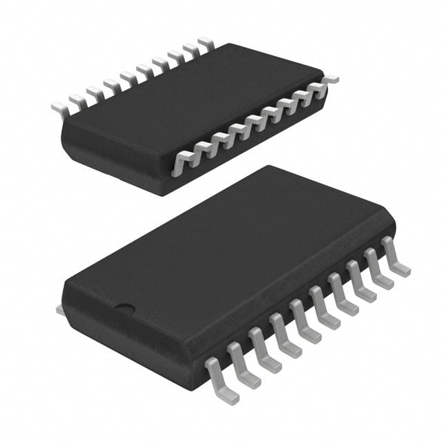
| 描述 | IC CFL LAMP DVR HV 20-SOIC |
| 产品分类 | |
| 品牌 | NXP Semiconductors |
| 数据手册 | |
| 产品图片 |
|
| 产品型号 | UBA20261T/1,518 |
| rohs | 无铅 / 符合限制有害物质指令(RoHS)规范要求 |
| 产品系列 | - |
| 供应商器件封装 | 20-SO |
| 其它名称 | 568-8541-6 |
| 制造商卷带宽度 | 24mm |
| 制造商卷带材料 | 塑料 |
| 制造商卷带直径 | 13"(330mm) |
| 包装 | Digi-Reel® |
| 图号 | 568; SOT163-1; D, T, TN2; 20 |
| 安装类型 | 表面贴装 |
| 封装/外壳 | 20-SOIC(0.295",7.50mm 宽) |
| 工作温度 | -40°C ~ 85°C |
| 标准包装 | 1 |
| 电压-电源 | 11.9 V ~ 13.8 V |
| 电流-灌/拉输出 | 540mA |
| 电流-电源 | 1.6mA |
| 类型 | CFL/TL 驱动器 |
| 调光 | 是 |
| 频率 | 40kHz ~ 100kHz |


- 商务部:美国ITC正式对集成电路等产品启动337调查
- 曝三星4nm工艺存在良率问题 高通将骁龙8 Gen1或转产台积电
- 太阳诱电将投资9.5亿元在常州建新厂生产MLCC 预计2023年完工
- 英特尔发布欧洲新工厂建设计划 深化IDM 2.0 战略
- 台积电先进制程称霸业界 有大客户加持明年业绩稳了
- 达到5530亿美元!SIA预计今年全球半导体销售额将创下新高
- 英特尔拟将自动驾驶子公司Mobileye上市 估值或超500亿美元
- 三星加码芯片和SET,合并消费电子和移动部门,撤换高东真等 CEO
- 三星电子宣布重大人事变动 还合并消费电子和移动部门
- 海关总署:前11个月进口集成电路产品价值2.52万亿元 增长14.8%


PDF Datasheet 数据手册内容提取
UBA20261/2 600 V and 350 V power IC for step dimmable CFLs Rev. 2 — 10 October 2011 Product data sheet 1. General description The UBA20261/2 are high-voltage power integrated circuits designed to drive and control high powered self-ballasted Compact Fluorescent Lamp (CFL) lighting applications operating at mains supply voltages of 120 V or 230 V. The IC includes a half-bridge power circuit consisting of two NMOST power MOSFETs, an advanced feature for step dimming and a lamp current controlled boost feature for boosting cold (amalgam) CFLs. The controller contains a CFL half-bridge drive function, a high-voltage level-shift circuit with integrated bootstrap diode, an oscillator function, a current control function for preheat and burn, a timer function and protection circuits. The UBA20261/2 are supplied using the dV/dt current charge supply circuit from the half-bridge circuit. Remark: The mains voltages given in this data sheet are AC voltages. 2. Features and benefits 2.1 Half-bridge features UBA20261: two internal 350 V, 1 , maximum 5 A NMOST half-bridge power MOSFETs UBA20262: two internal 600 V, 3 , maximum 2.7 A NMOST half-bridge power MOSFETs Integrated high-voltage level-shifter function with integrated bootstrap diode 2.2 Preheat and ignition features Coil saturation protection during ignition Adjustable saturation protection level Adjustable preheat time Adjustable preheat current Ignition lamp current detection 2.3 Lamp boost features Adjustable boost timing Fixed boost current ratio of 1.5 Gradually boost to burn transition timing
UBA20261/2 NXP Semiconductors 600 V and 350 V power IC for step dimmable CFLs 2.4 Dim features 4-level step dimming adjustment using a standard on/off mains switch Adjustable memory retention time for step dimming Adjustable minimum dimming level 2.5 Protection OverTemperature Protection (OTP) Capacitive Mode Protection (CMP) OverPower Protection (OPP) OverCurrent Protection (OCP) in both boost and burn states Power-down function 2.6 Other features Current controlled operation in both boost and burn state External power-down option 3. Applications UBA20261: Step-dimmable compact fluorescent lamps at power levels between 5W and 20W operating at 120Vmains voltage UBA20262: Step-dimmable compact fluorescent lamps at power levels between 5W and 20W operating at 230Vmains voltage 4. Ordering information Table 1. Ordering info rmation Type number Package Name Description Version UBA20261T/N1 SO20 plastic small outline package; 20leads; body width 7.5mm SOT163-1 UBA20262T/N1 SO20 plastic small outline package; 20 leads; body width 7.5mm SOT163-1 UBA20261_UBA20262 All information provided in this document is subject to legal disclaimers. © NXP B.V. 2011. All rights reserved. Product data sheet Rev. 2 — 10 October 2011 2 of 32
xxxx xxxxxxxxxxxxxxxxxxxxxxxxxxxxxx x xxxxxxxxxxxxxx xxxxxxxxxx xxx xxxxxx xxxxxxxxxxxxxxxxxxxxxxx xxxxxxxxxxxxxxxxxxxxxx xxxxx xxxxxx xx xxxxxxxxxxxxxxxxxxxxxxxxxxxxx xxxxxxxxxxxxxxxxxxxxxx xxxxxxxxxxx xxxxxxx xxxxxxxxxxxxxxxxxxx xxxxxxxxxxxxxxxx xxxxxxxxxxxxxx xxxxxx xx xxxxxxxxxxxxxxxxxxxxxxxxxxxxxxxx xxxxxxxxxxxxxxxxxxxxxxxx xxxxxxx xxxxxxxxxxxxxxxxxxxxxxxxxxxxxxxxxxxxxxxxxxxxxx xxxxxxxxxxx xxxxx x x P U 5 N roduct data sh BA20261_UBA20262 6VDD BOOTSTRAP 1168 DFSHS . Block XP Semic eet SUPPLY REVFOELRTEANGCEES DIVLIODGE IBCY 2 DLROIGVEICR SLHEIFVTEELR HS driverGHS 1179 HHBBOO dia ond 55 VV DDIIGGIITTAALL MEMORY T1E6M0S°PE1EN2RS0AO°TR8U0R°E LS driverGLS 210 SHLBSO gram uctor 5 V ANALOG 2 SLS s STATE LOGIC CAPACITIVE MODE DETECTOR 3 SLS + + VDD(stop) - - RESET Vth(capm)SLS A Rev. 2 — 10 October 2011 ll information provided in this document is subject to legal disclaimers. SGNCCDBP 111534 B1 OμPAORSETH ETIAM6T E/μAR 6++--0 μA 5 V LOGICCOUNTER DLISMOTGMEIEPCR POSPIWGTBRRBHEANOEEUORRIOSHTRL-TEIEDSDN-OUTATO N SST PSWS TT SSTTSAANATATTTT ATATASEETETETTEEEATE 4 2 LOGICLOGIC IGPONRIVINET2EHDI5OR EUμNCAAC UTCT ROUCRRRUER R++S--NERA+T-NET DTNUV EVTRDtph TAESVh(EdTt(TEhSeCIE(NOtLo)TiCSScgNOp)nTO/)(ROSCRLSRSI) 54 PLSGANTD 600 V and 350 V p o REFERENCE VOLTAGE LOGIC BOOST QA QB STEP DIM LEVEL SELECT w CURRENT CONTROLLED OSCILLATOR AMPLIFIER VMDL e 1.27 V + FRCEOQNUTERNOCLY VVDDIIMM__32 r IC + - I - OLTAA+-MP Vclamp(CSI) VDIM_1 dim2(CSI) dim3(CSI) 12 n.c. for ste UB © NXP B 25 μA V CSUERNRSEONRT DSR ∆V ∆V p dim A2 3 of 32 .V. 2011. All rights reserved. Fig 1. BlockR7 RdEiaFgram C8F C10I C11SI M9DL 001aam982 mable CFLs 0261/2
UBA20261/2 NXP Semiconductors 600 V and 350 V power IC for step dimmable CFLs 6. Pinning information 6.1 Pinning SLS 1 20 HBO SLS 2 19 HBO SLS 3 18 DHS LSAT 4 17 HBO PGND 5 16 FS UBA20261/2 VDD 6 15 SGND RREF 7 14 CB CF 8 13 CP MDL 9 12 n.c. CI 10 11 CSI 001aao278 Fig 2. Pin configuration for UBA20261/2 (SOT109-1) 6.2 Pin description Table 2. Pin description Symbol Pin Description SLS 1, 2, 3 source low-side switch[1] LSAT 4 coil saturation level input PGND 5 power ground[2] V 6 low voltage supply DD RREF 7 internal reference current input CF 8 voltage controlled oscillator capacitor MDL 9 minimum dimming level input CI 10 voltage controlled oscillator input integrating capacitor CSI 11 current feedback sense input n.c. 12 not connected CP 13 preheat timing capacitor CB 14 boost timing capacitor SGND 15 signal ground[2] FS 16 floating supply voltage HBO 17, 19, 20 half-bridge output; open output[3] DHS 18 high-voltage supply; drain high-side switch [1] The SLS pins are internally connected. [2] The PGND and SGND pins are internally connected. [3] The HBO pins are internally connected. UBA20261_UBA20262 All information provided in this document is subject to legal disclaimers. © NXP B.V. 2011. All rights reserved. Product data sheet Rev. 2 — 10 October 2011 4 of 32
UBA20261/2 NXP Semiconductors 600 V and 350 V power IC for step dimmable CFLs 7. Functional description The UBA20261/2 are ICs with integrated half-bridge MOSFETs in self-ballasted high-power CFLs. The UBA20261/2 have no dimming control input but instead, four preset fixed dimming levels. Only minor adjustment of the presets is possible. The UBA20261/2 are rated up to a maximum continuous rectified mains voltage of 350 V or 500 V, respectively and lamp power-up to 20W. The UBA20261/2 includes all functions necessary for preheat, ignition and boost operation of the lamp. In addition, the IC includes the four-step dimming feature and several protective features to safeguard CFL operation. The controller states are shown in Figure3. VDD = 0 RESET STATE VDD < VDD(rst) HOLD = 0 VDD > VDD(rst) VDD < VDD(rst) START-UP STATE VCP < Vth(rel)CP POWER-DOWN STATE (1) PREHEAT STATE (2) HOLD STATE (3) HOLD = 1 preheat time completed IGNITION STATE (4) Ignition_Detected VDD < VDD(stop) BOOST AND BURN (5) STATES 001aam763 (1) V < V and (HOLD = 0 OR V < V ). DD DD(start) CP th(rel)CP (2) V < V . DD DD(stop) (3) (End of ignition time AND HOLD = 0) OR VDD<VDD(stop). (4) End of ignition time AND HOLD = 1. (5) VCP < Vth(pd)CP, OR overcurrent fault time > 1⁄10 tph OR fbridge(max) detected in capacitive mode. Fig 3. State diagram UBA20261_UBA20262 All information provided in this document is subject to legal disclaimers. © NXP B.V. 2011. All rights reserved. Product data sheet Rev. 2 — 10 October 2011 5 of 32
UBA20261/2 NXP Semiconductors 600 V and 350 V power IC for step dimmable CFLs 7.1 Lamp start-up cycle 7.1.1 Reset state The UBA20261/2 are in the reset state when the supply voltage on the V pin is below DD the V level. In the reset state, part of the internal supply is turned off and all registers, DD(rst) counters and timers are undefined. The hold state latch is reset and both the high and low side power transistors are non-conductive. During power-up, the low voltage supply capacitor on the V pin is charged through the DD external start-up resistor. The start-up state is entered when the voltage on the V pin is DD above the V level. The UBA20261/2 enters the reset state when the supply voltage DD(rst) on the V pin drops below V . DD DD(rst) 7.1.2 Start-up state The start-up state is entered by charging the low voltage supply capacitor on the V pin DD through the external start-up resistor. At start-up, the High-Side (HS) transistor is non-conductive and the Low-Side (LS) transistor is conductive to enable charging of the bootstrap capacitor. This capacitor supplies the HS driver and Level shifter circuit connected between the FS and HBO pin. A DC reset circuit is integrated into the HS driver. This circuit ensures that below the FSpin lockout voltage, the output voltage V V is zero. GHS HBO When the start-up state is entered, the circuit only starts oscillating when the low voltage supply (V ) reaches the V value. The circuit always starts oscillating at f . DD DD(start) bridge(max) The circuit enters the preheat state as soon as the capacitor connected to the CP pin is charged above the V voltage level. To keep oscillating, V must be above th(CP)max DD V and below the V upper limit. DD(stop) DD(clamp) During the start-up state, the voltage on the CF pin is zero and on the CB pin is close to zero. The voltage on the CP pin rises just above V during the start-up state as th(CP)max shown in Figure9. 7.1.3 Preheat state After starting at f , the frequency decreases by charging capacitor C using an bridge(max) CI output current circuit. The preheat current sensor circuit controls the current output circuit, until the momentary value of the voltage across sense resistor R reaches the fixed SLS preheat voltage level (SLS pin). At this level, the current of the preheat current sensor reaches the charge and discharge balanced state on capacitor C to set the half-bridge CI frequency. The preheat time consists of eight saw-tooth pulses at the CP pin. The preheat time begins as soon as the capacitor on the CP pin is charged above V value. During th(CP)max the preheat time, the current feedback sensor circuit (input CSI pin) is disabled. To increase noise immunity, an internal filter of 30ns is included at the SLS pin. If the level on the V pin drops below V during preheat, the preheat state is DD DD(stop) immediately stopped and the circuit enters the hold state. The hold state delays a new preheat cycle by a fixed delay time. A fixed voltage drop on the preheat capacitor C and CP the fixed discharge current on the CP pin are used to set the delay time. UBA20261_UBA20262 All information provided in this document is subject to legal disclaimers. © NXP B.V. 2011. All rights reserved. Product data sheet Rev. 2 — 10 October 2011 6 of 32
UBA20261/2 NXP Semiconductors 600 V and 350 V power IC for step dimmable CFLs New preheat cycles start after the CP pin level slowly discharges until V <V and CP th(rel)CP recharges above V provided V > V (see Figure5). th(CP)max DD DD(start) f (kHz) 100 start frequency CFL ignition A B C preheat frequency 100 % boost bottom ~22 kHz time (s) preheat ignition boost transition burn 001aam764 Fig 4. CFL frequency from start to burn state 7.1.4 Ignition state After the preheat state has been completed, the ignition state is entered. In the ignition state, the frequency sweeps down on the CI pin due to capacitor C charging at a fixed CI current as shown in Figure4. During this continuous decrease in frequency, the circuit approaches the resonant frequency of the resonant tank (L2, C5). This action causes a high voltage across the lamp to ignite the lamp. The ignition current sensor circuit which monitors the voltage over resistor R (see Figure12) detects lamp ignition. CSI If the voltage on pin CSI is above the typical ignition detection threshold voltage level of 0.6 V, lamp ignition is detected. The system changes from ignition state to either the boost or burn state. If ignition not is detected, the frequency drops further to the minimum half-bridge frequency f frequency. To avoid repeated ignition attempts and overheating of the bridge(min) application due to lamp damage, the IC only tries to ignite the lamp twice after power-up. The ignition attempt counter increments at the end of the ignition enabling time when the lamp ignition threshold voltage on the CSI pin is not exceeded. The ignition enabling time is typically 1⁄ of the preheat time t . If a second ignition attempt also exceeds the ignition 4 ph time-out period, the IC enters the power-down state (see Figure5). UBA20261_UBA20262 All information provided in this document is subject to legal disclaimers. © NXP B.V. 2011. All rights reserved. Product data sheet Rev. 2 — 10 October 2011 7 of 32
UBA20261/2 NXP Semiconductors 600 V and 350 V power IC for step dimmable CFLs voltage (V) 1st failed 2nd failed 5 V VCP ignition ignition Vth(CP)max attempt attempt Vth(CP)min discharge to 0 V Vth(rel)CP startup 1st preheat 2nd preheat HOLD STATE POWER DOWN STATE time time time tph ten(ign) td(restart) tph ten(ign) 1st ignition restart 2nd 2nd ignition enabling time delay time startup enabling time 0 V time (s) 001aan537 Fig 5. Retry cycle 7.1.5 Boost state and transition to burn state When ignition is detected, by measuring lamp current on the CSI pin, the circuit enters the boost state. Figure7 shows the boost and burn state in more detail. In the boost state, the nominal burn state lamp current can be increased with a fixed boost ratio of 1.5:1. This ratio boosts the slow luminescence increase of a cold amalgam CFL lamp, provided the IC is in the DIM_1 mode. If the IC is at a temperature (T ) before entering the boost j(bp)bst state, the burn state is bypassed. A boost timing circuit is included to determine the boost time and transition to burn time. The circuit consists of a clock generator comprising C , R and a 64-step counter. CB ext(RREF) When the timer is not operating, C is discharged below the V level of 1.1 V. This CB th(CB)min voltage, approximately 0.6 V, is still higher than the level at which the comparator on C CB detects if the CB pin is shorted to ground. The boost time consists of 63 saw-tooth pulses on the CB pin, automatically followed by the transition time at the CP pin. The 32 saw-tooth pulses form the transition time from boost to burn and enables a smooth transition between the current controlled boost and burn state. The total transition time is approximately four times the preheat time (see Figure6). UBA20261_UBA20262 All information provided in this document is subject to legal disclaimers. © NXP B.V. 2011. All rights reserved. Product data sheet Rev. 2 — 10 October 2011 8 of 32
UBA20261/2 NXP Semiconductors 600 V and 350 V power IC for step dimmable CFLs voltage (V) 5 V VCP 1 32 Vth(CP)max 4.5 V Vth(CP)min 3.8 V Vth(CB)max 3.6 V VCB Vth(CB)min 1.1 V 1 2 61 62 63 0.6 V ignition boost transition burn 0 V time (s) 001aam765 Fig 6. Boost timing In the boost state, a lamp current feedback control is implemented to improve lamp stability (see Section7.1.6). The lamp current has a fixed ratio of 1.5 compared to the burn state to boost the slow luminescence increase of a cold CFL lamp. In the boost to burn transition time, there is a slow 15-step ratio decrease from 1.5down to1. The preheat timer is reused for the transition to burn time and the boost ratio is gradually decreased in 15 steps from 1.5to1, within 32 saw-tooth pulses on the CP pin. Using the application values for C and R a boost time of more than 300s is possible. In CB ext(RREF), addition to boost bypass at a temperature of T (80 C), a temperature protection j(bp)bst function is implemented during boost state of T (120 C). If the temperature j(end)bst passes this level during boost, the transition timer is immediately started to enter the burn state faster. Effectively this reduces the boost time (see Figure4 [B]). The boost state current boost does not start in dim modes DIM_2, DIM_3 or MDL (seeFigure4 [A]). Remark: If the CB pin is short circuited to ground, the boost function is disabled. In such a situation, the bottom frequency f is 1.8 times higher than the boost bottom bridge(min) frequency f . bridge(bst)min 7.1.6 Burn state After the boost state or when it is bypassed, the burn state starts. The lamp current sensor circuit remains enabled (see Figure4[A]). The voltage across sense resistor R , is CSI measured by the CSI (Current Sense Input) pin. It is then passed through a Double-Sided Rectifier (DSR) circuit and fed towards an Operational Transconductor Amplifier (OTA). When the RMS voltage on the CSI pin reaches the actual internal reference level, the lamp current sensor circuit takes over control of the lamp current. The internal current output of the OTA is transferred using an integrator on the CI pin to the input for Voltage Controlled Oscillator (VCO). The VCO regulates the frequency and as a result, the lamp current. UBA20261_UBA20262 All information provided in this document is subject to legal disclaimers. © NXP B.V. 2011. All rights reserved. Product data sheet Rev. 2 — 10 October 2011 9 of 32
UBA20261/2 NXP Semiconductors 600 V and 350 V power IC for step dimmable CFLs BOOST AND BURN STATES Dim_1 state AND Boost boost timer running Temp < Tj(bp)bst AND 00 NOT Boost_Disable 01 Boost_ratio = 1 Boost_ratio = 1.5 burn select boost NOT (Boost OR Boost transition) Temp < Tj(otp) - Tj(otp)(hys) Temp > Tj(bp)(bst) OR Vi(CSI) = Votp(CSI) Vi(CSI) = Vdamp(CSI) Temp > Tj(end)bst Boost_Disable (66 % level) (100 % level) OR boost timer ended Temp > Tj(otp) 10 11 burn boost transition boost_transition timer ended OR temp > Tj(otp) 001aam767 Fig 7. Boost and burn state machine 7.1.7 Hold state The hold state is a special state that reduces lamp flicker at deep dim levels, on or near dim and ignition threshold levels. The IC enters the hold state after an ignition failure or when the low supply voltage V drops below V in the ignition or preheat states DD DD(stop) (see Figure3). A repeated drop in supply voltage below V in preheat or ignition states, does not DD(stop) increment the ignition attempt counter. The hold state is entered, delaying a new preheat cycle with the same time delay/mechanism by the hold state retention time as shown in Figure5. When CP is below V , the IC is released from the hold state and moves to the th(rel)CP start-up state as shown in Figure3. Alternatively, the hold state ends when the supply voltage drops below V and the IC is reset. DD(rst) With a 470nF capacitor on the CP pin, the typical hold state retention delay is between 1s and 1.7s. This delay is dependent on where the preheat cycle was cut-off on the rising or falling edge of the preheat timing. The retention time for a failed ignition always starts from the top of the rising edge on the CP pin (see Figure5). In the hold state, a hold state latch is set (hold state latch = 1) and the oscillator is stopped. In addition, the HS transistor is non-conductive and the LS transistor is conducting. The voltage on the V pin alternates between V and V until the voltage on DD DD(start) DD(stop) the CP pin reaches V (see Figure5). The alternating supply voltage is caused by th(rel)CP the current drawn by the IC supply pin V . The supply current is less than 220 A, when DD UBA20261_UBA20262 All information provided in this document is subject to legal disclaimers. © NXP B.V. 2011. All rights reserved. Product data sheet Rev. 2 — 10 October 2011 10 of 32
UBA20261/2 NXP Semiconductors 600 V and 350 V power IC for step dimmable CFLs the supply voltage V rises between V and V . Typically, the supply current DD DD(stop) DD(start) is 2 mA when V falls between V and V . More current is drawn during the DD DD(start) DD(stop) fall in V because the internal analog supply is turned on when V >V . This DD DD DD(start) function enables the comparators to monitor the voltage on the CP pin and if the supply voltage V falls below V . DD DD(stop) 7.2 Oscillation and timing 7.2.1 Oscillator control The internal oscillator is a VCO which generates a saw-tooth waveform between the V level and 0 V. Capacitor C , resistor R and the voltage on the CI pin th(CF)max CF ext(RREF) determine the saw-tooth frequency. R and C determine the minimum and ext(RREF) CF maximum switching frequencies. Their ratio is internally fixed. Two ratios are available, the ratio between f and f is 2.5 and the ratio between f and bridge(max) bridge(min) bridge(max) f is 4.6. The saw-tooth frequency is twice the half-bridge frequency. bridge(bst)min Transistors HS (Q1) and LS (Q2) are switched to conducting at a duty cycle of approximately 50%. An overview of the oscillator signal and driver signals is shown in Figure8. The oscillator starts oscillating at f . The non-overlap time between the bridge(max) gate driver signals V and V is t . GLS GHS no voltage (V) VCF 0 tdch V(GHS-HBO) 0 VGLS tno tno 0 VHBO 0 time (s) 001aam766 Fig 8. Saw-tooth, gate driver and half-bridge output signals 7.2.2 Combined timing circuit A combined timing circuit is used to determine the preheat time, ignition enabling time and overcurrent time (see Figure9). C , R and the counter comprise the clock CP ext(RREF) generator circuit. When the timer is not running, C is charged to 5 V. The timing circuit CP UBA20261_UBA20262 All information provided in this document is subject to legal disclaimers. © NXP B.V. 2011. All rights reserved. Product data sheet Rev. 2 — 10 October 2011 11 of 32
UBA20261/2 NXP Semiconductors 600 V and 350 V power IC for step dimmable CFLs starts operating after the start-up state when the V supply voltage has reached V DD DD(start) and the voltage on the CP pin passes V . The preheat time consists of eight th(CP)max saw-tooth pulses on the CP pin as shown in Figure9. The maximum ignition enabling time after the preheat phase is two complete saw-tooth pulses. During the boost and burn state, part of the timer is used to generate the maximum overcurrent time (more than one half of the saw-tooth pulse). If a continuous overcurrent is detected, the timer starts. voltage (V) ignition enabling time 5 V VCP Vth(CP)max 4.5 V Vth(CP)min 3.8 V CFL ignitionovercurrent ignition fault time time startup preheat time boost-burn power down time 0 V time (s) 001aam768 Fig 9. Timing diagram for preheat, ignition and overcurrent 7.3 Step dimming The UBA20261/2 uses the step dimming method of dimming a lamp load. This method enables the lamp to operate in four different light output level modes including full power. The four different dim level modes can be selected by toggling the supply voltage which is made possible by toggling the mains voltage switch. To change the dim step, the low supply voltage must be above V . In addition, the DD(start) voltage must drop below V , irrespective of whether the IC is in the preheat, ignition, DD(rst) boost or burn states (see Figure10). The discharge time of capacitor C (while the V power supply is off) sets step memory CP DD retention time. When the voltage on the CP pin drops below V (2V typical), the ret(dim)CP step memory is lost. The next time the supply is powered on, the lamp turns on at full brightness. Using the default components, the retention time is 3s. The retention time calculation can be found in Section11 on page23. UBA20261_UBA20262 All information provided in this document is subject to legal disclaimers. © NXP B.V. 2011. All rights reserved. Product data sheet Rev. 2 — 10 October 2011 12 of 32
UBA20261/2 NXP Semiconductors 600 V and 350 V power IC for step dimmable CFLs voltage dim step (V) change VDD(start) VDD VDD(stop) lamp on lamp off lamp on old dim level new dim level VDD(rst) 5 VCP Vret(dim)CP 0 time (s) retention start-up 001aam769 Fig 10. Supply voltage cycle for dim step change Four internal references determine the actual internal set point levels used for the different step dim levels. Depending on the selected dim level, the current control feedback loop regulates the voltage on the CSI pin. In this way, it ensures that V is equal to one of i(CSI) the selected internal set point voltages. The sequence of the four dim steps shown in Figure11 is as follows: • The lamp is switched off longer than the memory retention time: the IC starts up in the DIM_1 mode (lamp is 100% on, no dimming) • After lamp off/on toggling, the IC twice enters DIM_2 mode: the lamp is dimmed to approximately 66%(1) of its initial light output • The next lamp off/on toggling, the IC enters DIM_3 mode: the lamp is dimmed approximately 33%(1) of its initial light output • Toggling the lamp off/on again: the IC enters the MDL (Minimum Dimming Level) mode. This level equals approximately 10%(1) of the initial light output • Renewed toggling enters the DIM_1 mode again. Where (1) = R = 2k MDL UBA20261_UBA20262 All information provided in this document is subject to legal disclaimers. © NXP B.V. 2011. All rights reserved. Product data sheet Rev. 2 — 10 October 2011 13 of 32
UBA20261/2 NXP Semiconductors 600 V and 350 V power IC for step dimmable CFLs Vi(CSI) VRMS 1.2 Vclamp(CSI) DIM_1 1.0 Internal clamp 100 % 0.8 VDD off-on toggle 0.6 VDD off-on toggle DIM_2 0.4 (1) ∆Vdim2(CSI) 0.2 DIM_3 ∆Vdim3(CSI) (1) Vi(CSI) = VMDL MDL 0 (1) = VDD off-on toggle 001aam770 Fig 11. Voltage on the CSI pin as function of dim step As the internal step reference voltages are independent from the mains voltage, the lamp current output is kept constant. Making the lamp current output not susceptible to line voltage fluctuations. The MDL level sets the minimum lamp current level and is adjusted using the MDL pin. An accurate minimum dimming voltage level is set using an internal reference current and an external resistor R . The internal reference current is derived MDL from the internal band gap reference circuit and resistor R . The other two step ext(RREF) dimming levels are set at a fixed voltage offset referenced to the adjusted MDL level. This means that these levels shift by the same voltage as the MDL shifts. When the MDL level is at the default level, the light output in DIM_2, DIM_3 and MDL modes is approximately 66%, 33% and 5% from nominal. 7.4 Protection functions and Power-down mode 7.4.1 Coil saturation protection CSP is integrated into the IC to allow the use of small CFL lamps and use of small coils. Saturation of these coils is detected and excessive overcurrent due to saturation is prevented. CSP is only enabled during the ignition state. A cycle-by-cycle control mechanism is used to limit voltages and currents in the resonant circuit when there is no or delayed ignition. It prevents coil saturation, limits high peak currents and the dissipation in the half-bridge power transistors. Coil saturation is detected by monitoring the voltage across the R resistor. A trigger is SLS generated when this voltage exceeds the V level. When saturation is detected, a th(sat)SLS fixed current I is injected into the C capacitor to shorten the half-bridge o(sat)CF CF UBA20261_UBA20262 All information provided in this document is subject to legal disclaimers. © NXP B.V. 2011. All rights reserved. Product data sheet Rev. 2 — 10 October 2011 14 of 32
UBA20261/2 NXP Semiconductors 600 V and 350 V power IC for step dimmable CFLs switching cycle. The injected current is maintained until the end of the switching cycle. This action immediately increases the half-bridge switching frequency. Additionally, for each successive cycle that coil saturation is detected, capacitor C discharges enabling CI ignition time-out detection in the ignition state. CSP is triggered when the voltage on the SLS pin exceeds V (typically 2.5V). The th(sat)SLS voltage V on the SLS pin is determined by the external resistor R value and also i(SLS) SLS sets the preheat current. Using an internal reference source current and external resistor R , an accurate setting LSAT for the coil saturation threshold level V is possible. When resistor R is not th(sat)SLS LSAT mounted, the V level is internally clamped at 2.5V. It is mandatory for stability th(sat)SLS reasons to connect C in parallel to R even when R is not mounted. LSAT LSAT LSAT 7.4.2 Overcurrent protection OCP is active in both the burn and boost states but not during boost transition. Overcurrent is detected, when the peak voltage of the absolute value across the current sense resistor connected to the SLS pin exceeds the OCP reference level V . A th(ocp)SLS current I is then sunk from the capacitor connected to the CP pin for the next full o(CP) cycle. If overcurrent is not present at the end of this cycle, the current is disabled. A current, equal to I is sourced to the CP pin instead. If overcurrent occurs in more than half the o(CP) number of cycles, a net discharging of the capacitor connected to the CP pin occurs. When the voltage on the CP pin drops below V , the IC enters Power-down mode. th(CP)min During a continuous overcurrent condition, the overcurrent fault time of t takes fault(oc) 1⁄ t after which the IC enters Power-down mode. The V level is the same as 9 ph th(ocp)SLS the V level during the ignition state. th(sat)SLS 7.4.3 Overpower protection OPP is active in the boost and burn state. The lamp current is limited and regulated in all dim step states to the internal dim step reference voltage levels. These reference voltage levels are derived from an internal reference voltage. Consequently, supply voltage fluctuations in the mains supply voltage during overvoltage situations do not affect these reference voltage levels. When the lamp is in the first dim mode (no dimming), the current is limited and regulated to the nominal lamp current. In addition, in the boost state, the first dim mode boosted by a factor of 1.5. 7.4.4 Capacitive mode protection CMP is active in the ignition, burn and boost states and during boost transition. The signal across resistor R also provides information about the half-bridge switching behavior. SLS When conditions are normal, the current flows from the LS transistor source to the half-bridge when the LS transistor is switched on. This results in a negative voltage on the SLS pin. As the circuit yields to capacitive mode, the voltage becomes smaller and eventually reverses polarity. CMP prevents this action by checking if the voltage on the SLS pin is above the V level. th(capm)SLS UBA20261_UBA20262 All information provided in this document is subject to legal disclaimers. © NXP B.V. 2011. All rights reserved. Product data sheet Rev. 2 — 10 October 2011 15 of 32
UBA20261/2 NXP Semiconductors 600 V and 350 V power IC for step dimmable CFLs If the voltage across resistor R is above the V threshold when the LS SLS th(capm)SLS transistor is switched on, the circuit assumes that it is in capacitive mode. When capacitive mode is detected, the currents from the OTA, which normally regulate the lamp current, are disabled. Then the capacitive mode sink current I is enabled. o(CI) The capacitive mode sink current starts to discharge the capacitor/resistor circuitry on theCI pin and as a result, gradually increases the half-bridge frequency. Discharging continues for the remainder of the current switching cycle ensuring the total current on the CI pin is equal to the sink current. If capacitive mode persists, the action is repeated until capacitive mode is no longer detected. If capacitive mode is no longer detected, the OTA takes over the regulation again. If the conditions causing capacitive mode persist, OTA regulates the system back towards capacitive mode and the protection takes over again. The system operates on the edge of capacitive mode. When in the boost and burn states, the half-bridge load is capacitive at higher frequencies, CMP eventually drives the half-bridge to the maximum frequency f . bridge(max) This causes the IC to enter Power-down mode. 7.4.5 Overtemperature protection The OTP circuit is designed to prevent the device from overheating in hazardous environments. The circuit is triggered when the temperature exceeds the maximum temperature value T . OTP changes the lamp current to the level equal to the V j(otp) otp(CSI) level. This condition remains until the temperature decreases by 20C=T . After j(otp)hys this decrease in temperature, the lamp current level returns to the nominal level. 7.4.6 Power-down mode Power-down mode is entered when: • The overcurrent time exceeds the maximum overcurrent fault time t or if the fault(oc) overcurrent occurs in more than half the number of cycles when V is reached th(CP)min • If during boost or burn state, f is reached due to capacitive mode detection bridge(max) • two consecutive failed lamp ignition attempts In Power-down mode, the oscillator is stopped, the HS transistor is non-conductive and the LS transistor is conductive. The V supply is internally clamped. The circuit is DD released from Power-down mode by lowering the low voltage supply below V (mains DD(rst) switch reset). An option is available which enables the IC to enter Power-down mode using external logic. The external power-down option is only available when the IC is in the boost or burn state. The CP pin is used to enable the external power-down option. When the CP pin is connected using a 10k resistor to the PGND pin or the SGND pin, V is pulled below CP V . The IC then enters Power-down mode. th(pd)CP Remark: Do not connect the CP pin directly to pins PGND or SGND. Always connect in series to pins PGND or SGND with a 10k resistor. This action avoids the IC being not starting up because of excessive currents flowing during the reset and start-up states. UBA20261_UBA20262 All information provided in this document is subject to legal disclaimers. © NXP B.V. 2011. All rights reserved. Product data sheet Rev. 2 — 10 October 2011 16 of 32
UBA20261/2 NXP Semiconductors 600 V and 350 V power IC for step dimmable CFLs 8. Limiting values Table 3. Limiting valu es In accordance with the Absolute Maximum Rating System (IEC 60134). Symbol Parameter Conditions Min Max Unit General R external resistance on fixed nominal value 33 k 30 36 k ext(RREF) pin RREF SR slew rate on pins HBO with respect to PGND 4 +4 V/ns T junction temperature 40 +150 C j T ambient temperature P=0.8W 40 +85 C amb T storage temperature 55 +150 C stg Currents I input current on pin CF 0 200 A i(CF) I peak drain current UBA20261; DM HS; T <T ; I =I =I - 5 A j j(max) DM DHS HBO LS; T <T ; I =I =I - 5 A j j(max) DM HBO o(SLS) UBA20262; HS; T <T ; I =I =I - 2.7 A j j(max) DM DHS HBO LS; T <T ; I =I =I - 2.7 A j j(max) DM HBO o(SLS) I drain current UBA20261: D HS; RMS current at P=0.5W; T =T ; - 0.54 A j j(max) I =I =I D DHS HBO LS; RMS current at P=0.5W; T =T ; - 0.54 A j j(max) I =I =I D HBO o(SLS) UBA20262: HS; RMS current at P=0.5W; T =T ; - 0.31 A j j(max) I =I =I D DHS HBO LS; RMS current at P=0.5W; T =T ; - 0.31 A j j(max) I =I =I D HBO o(SLS) Voltages V voltage on pin DHS UBA20261: DHS operating at T = 25 C - 350 V amb operating at T = 25 C - 340 V amb UBA20262: operating - 500 V during 1 s - 600 V V voltage on pin FS with respect to HBO 0.3 +14 V FS V supply voltage 0.3 +14 V DD V input voltage on pin CSI 5 +5 V i(CSI) V input voltage on pin 6 +6 V i(SLS) SLS V voltage on pin CI 0 3.5 V CI V voltage on pin LSAT 0 5 V LSAT V voltage on pin MDL LPF used as input pin 0 5 V MDL UBA20261_UBA20262 All information provided in this document is subject to legal disclaimers. © NXP B.V. 2011. All rights reserved. Product data sheet Rev. 2 — 10 October 2011 17 of 32
UBA20261/2 NXP Semiconductors 600 V and 350 V power IC for step dimmable CFLs Table 3. Limiting values …continued In accordance with the Absolute Maximum Rating System (IEC 60134). Symbol Parameter Conditions Min Max Unit ESD V electrostatic discharge human body model: 2000 +2000 V ESD voltage all pins, except pins 16, 17, 18, 19 and 20 pins 16, 17, 18, 19 and 20 1000 +1000 V charged device model: 400 +400 V all pins 9. Thermal characteristics Table 4. Thermal cha racteristics Symbol Parameter Conditions Typ Unit R thermal resistance from junction to in free air; SO20 package on 56 K/W th(j-a) ambient JEDEC2S2P board UBA20261_UBA20262 All information provided in this document is subject to legal disclaimers. © NXP B.V. 2011. All rights reserved. Product data sheet Rev. 2 — 10 October 2011 18 of 32
UBA20261/2 NXP Semiconductors 600 V and 350 V power IC for step dimmable CFLs 10. Characteristics Table 5. Characterist ics V =13 V; V V =13 V; T = 25 C; settings according to default setting (see Table6 on page26), all voltages DD FS HBO amb referenced to PGND and SGND, positive currents flow into the UBA20261/2, unless otherwise specified. Symbol Parameter Conditions Min Typ Max Unit Start-up state Pin V DD V reset supply voltage HS switch = off; LS switch = on 5.7 6.2 6.7 V DD(rst) V stop supply voltage 9.6 10 10.4 V DD(stop) V start supply voltage 11.9 12.4 12.9 V DD(start) V hysteresis of supply voltage start-stop 2.2 2.4 2.6 V DD(hys) V clamp supply voltage I = 5 mA 13 13.4 13.8 V DD(clamp) DD(clamp) I clamp supply current V = 14V 20 30 - mA DD(clamp) DD(clamp) I start-up supply current V = 9 V - 190 220 A DD(startup) DD I power-down supply current V = 9 V - 190 220 A DD(pd) DD I supply current default setting; V =V ; [1] - 1.6 2 mA DD CI CI(clamp) V =0V CB High-voltage supply Pins DHS, HBO and FS I leakage current UBA20261: 300V on high-voltage - - 30 A leak pins UBA20262: 500V on high-voltage - - 30 A pins Voltage controlled oscillator Output pin CI V maximum voltage on pin CI 2.7 3 3.3 V CI(max) V headroom voltage on pin CI V = V +V ; burn - 80 - mV hr(CI) clamp(CI) hr(CI) CI(max) and boost state Output pin CF f minimum bridge frequency C = 100 pF; V = V ; [2] 38 40 42 kHz bridge(min) CF CI clamp(CI) V =0V CB f maximum bridge frequency C = 100 pF; V = 0 V [2] 88 100 112 kHz bridge(max) CF CI f minimum boost bridge frequency C = 100 pF; V = V [2] 21 22 23 kHz bridge(bst)min CF CI clamp(CI ) t non-overlap time V rising edge 1.3 1.5 1.7 s no HBO V falling edge 1.3 1.5 1.7 s HBO V maximum threshold voltage on pin C =100 pF; V =V ; 2.4 2.5 2.6 V th(CF)max ext(CF) CI clamp(CI) CF V =0V CB I boost output current on pinCF V =1.5V; V =V 12.3 11.8 11.3 A o(bst)CF CF CB clamp(CI ) I minimum output current on pinCF V =1.5V; V =0V; 22.8 21.8 20.8 V o(CF)min CF CB V =V CI clamp(CI ) I maximum output current on pinCF V =1.5V; V =0V 67 60 53 A o(CF)max CF CB UBA20261_UBA20262 All information provided in this document is subject to legal disclaimers. © NXP B.V. 2011. All rights reserved. Product data sheet Rev. 2 — 10 October 2011 19 of 32
UBA20261/2 NXP Semiconductors 600 V and 350 V power IC for step dimmable CFLs Table 5. Characteristics …continued V =13 V; V V =13 V; T = 25 C; settings according to default setting (see Table6 on page26), all voltages DD FS HBO amb referenced to PGND and SGND, positive currents flow into the UBA20261/2, unless otherwise specified. Symbol Parameter Conditions Min Typ Max Unit Power transistors R on-state resistance UBA20261: on HS; I = 1.1 A; T =25C - 1 1.3 DHS j LS; I = 1.1 A; T =25C - 1 1.3 HBO j UBA20262: HS; I = 1.1 A; T = 25C - 3 3.6 DHS j LS; I = 1.1 A; T =25C - 3 3.6 HBO j R /R on-state resistance ratio R at - 1.7 - on(150) on(25) on (150Cto25 C) T =150C/R atT =25C j on j Boot strap diode V forward voltage bootstrap diode; I =5mA; 1.3 1.7 2.1 V F FS (V =V -V ) F DD FS Preheat current sensor Input pin SLS I input current on pin SLS V =0.4V - - 1 A I(SLS) i(SLS) V preheat voltage on pin SLS [3] 0.57 0.60 0.63 V ph(SLS) Output pin CI I source output current on pin CI V =2V; V <0.6V 10.6 9.6 8.6 A o(source)CI CI i(SLS) I sink output current on pin CI V =2V; V <0.6V 26 29 32 A o(sink)CI CI i(SLS) Preheat timer, ignition timer and overcurrent fault timer t preheat time C = 470 nF; R = 33k - 0.93 - s ph CP ext(RREF) t ignition enable time C = 470 nF; R = 33k - 0.22 - s en(ign) CP ext(RREF) t overcurrent fault time C = 470 nF; R = 33k; - 0.1 - s fault(oc) CP ext(RREF) initial voltage V =5V CP t dimming retention time C = 470 nF; R = 33k; - 2.8 - s ret(dim) CP ext(RREF) initial voltage V =5V CP I output current on pin CP V =4.1V; source (); sink (+) 5.5 5.9 6.3 A o(CP) CP I dimming retention current on Current into pin CP; V =0V; - 0.5 - A ret(dim)CP DD pinCP initialV = 5V CP V minimum threshold voltage on pin V =0V, V =2V - 3.8 - V th(CP)min CF CI CP V maximum threshold voltage on V =0V, V =2V - 4.5 - V th(CP)max CF CI pinCP V hysteresis voltage on pin CP 0.6 0.7 0.8 V hys(CP) I pull-up current on pin CP V = 3.8V - 60 - A pu(CP) CP V dimming retention voltage on V =0V - 2 - V ret(dim)CP DD pinCP V power-down threshold voltage on burn state; 10 k connected in - 1 - V th(pd)CP pin CP series V release threshold voltage on pin CP hold state - 2.7 - V th(rel)CP UBA20261_UBA20262 All information provided in this document is subject to legal disclaimers. © NXP B.V. 2011. All rights reserved. Product data sheet Rev. 2 — 10 October 2011 20 of 32
UBA20261/2 NXP Semiconductors 600 V and 350 V power IC for step dimmable CFLs Table 5. Characteristics …continued V =13 V; V V =13 V; T = 25 C; settings according to default setting (see Table6 on page26), all voltages DD FS HBO amb referenced to PGND and SGND, positive currents flow into the UBA20261/2, unless otherwise specified. Symbol Parameter Conditions Min Typ Max Unit Boost timer Pin CB t boost time C =470nF; T <80C - 148 - s bst CB j I output current on pin CB V =2.35V; source (); sink (+) 0.8 1 1.2 A o(CB) CB V minimum threshold voltage on pin - 1.1 - V th(CB)min CB V maximum threshold voltage on pin - 3.6 - V th(CB)max CB V hysteresis voltage on pin CB 2.3 2.5 2.7 V hys(CB) T boost bypass junction temperature T sensed at end of ignition time 65 80 95 C j(bp)bst j T boost end junction temperature T during boost time 105 120 135 C j(end)bst j I boost disable detection current V =0V 30 25 20 A det(dis)bst CB t transition time from boost to burn C =470nF; T <80C - 3.6 - s t(bst-burn) CP j Pin CSI N lamp current boost ratio V in boost state versus V in 1.4 1.5 1.6 V LCBR i(CSI) i(CSI) burn state; default start-up state (nodimming) Coil saturation protection and overcurrent detection Input: pin SLS V saturation threshold voltage on pin ignition state; R =47 k 1.10 1.18 1.25 V th(sat)SLS LSAT SLS V overcurrent protection threshold ignition state; R =47 k 1.10 1.18 1.25 V th(ocp)SLS LSAT voltage on pin SLS t leading edge blanking time detection disabled for first part of - 800 - ns leb GLS time Input: pin LSAT: I source current on pin LSAT V =1.2V 26.3 25 23.7 A source(LSAT) LSAT V clamp voltage on pin LSAT R = ;C =1nF 2.3 2.5 2.7 V clamp(LSAT) LSAT LSAT Output pin CI I sink output current on pin CI V = 2 V; V > V ; cycle 26 29 32 A o(sink)CI CI i(SLS) th(sat)SLS clocked Output: pin CF: I saturation output current difference V = 1.5 V; ignition state; - 160 - A o(sat)CF CF on pin CF LSswitch=on Ignition current detection Input pin CSI V ignition detection threshold voltage [3] 0.55 0.6 0.65 V th(det)ign(CSI) on pin CSI t minimum ignition detection pulse V = 0.75V square pulse 685 885 1085 ns w(det)ign(min) th(det)ign(CSI) width UBA20261_UBA20262 All information provided in this document is subject to legal disclaimers. © NXP B.V. 2011. All rights reserved. Product data sheet Rev. 2 — 10 October 2011 21 of 32
UBA20261/2 NXP Semiconductors 600 V and 350 V power IC for step dimmable CFLs Table 5. Characteristics …continued V =13 V; V V =13 V; T = 25 C; settings according to default setting (see Table6 on page26), all voltages DD FS HBO amb referenced to PGND and SGND, positive currents flow into the UBA20261/2, unless otherwise specified. Symbol Parameter Conditions Min Typ Max Unit Capacitive mode detection Input pin SLS V capacitive mode threshold voltage [4] 15 5 0 mV th(capm)SLS on pin SLS Output pin CI I sink output current on pin CI V > V ; V = 2 V; 26 29 32 A o(sink)CI i(SLS) th(capm)SLS CI ignition state or boost and burn state Lamp current sensor and dimming control Input pin CSI R input resistance on pin CSI V = 1 V 1 - - M i(CSI) i(CSI) V = 1 V 40 50 60 k i(CSI) V input voltage on pin CSI rectification linear for operation 2.5 - +2.5 V i(CSI) minimum dim level; 44 50 56 mV R =33k; R =2k ext(RREF) MDL V clamping voltage on pin CSI RMS voltage; clamp active; default - 1 - V clamp(CSI) start-up burn state; 100 % on V dimming 2 voltage difference on RMS voltage; offset from V at 330 350 370 mV dim2(CSI) i(CSI) pinCSI DIM_2 compared to MDL V dimming 3 voltage difference on pin RMS voltage; offset from V at 90 100 110 mV dim3(CSI) i(CSI) CSI DIM_3 compared to MDL Output pin CI I output current on pin CI burn state; source and sink; 85 95 105 A o(CI) V =2V; source () and sink (+) CI Input pin MDL (minimum dimming level) I source current on pin MDL 26.3 25 23.7 A source(MDL) V voltage on pin MDL R = 33 k; R = 2 k - 50 - mV MDL ext(RREF) MDL Temperature protection T overtemperature protection junction 145 160 170 C j(otp) temperature T hysteresis overtemperature 10 20 30 C j(otp)hys protection junction temperature Input pin CSI V overtemperature protection voltage RMS voltage; R = 33 k; 380 400 420 mV otp(CSI) ext(RREF) on pin CSI R =2 k; T >T T MDL j j(opt) j(hys)(otp) [1] See Table6 on page26 for the default setting. [2] The half-bridge output switching frequency (HBO). The saw-tooth frequency on pin CF is twice as high. [3] Data sampling of V is performed at the end of the LS power MOSFET conduction period in preheat state. ph(SLS) [4] Data sampling of V is performed at the start of conduction of the LS power MOSFET, in all states with oscillator active. th(capm)SLS UBA20261_UBA20262 All information provided in this document is subject to legal disclaimers. © NXP B.V. 2011. All rights reserved. Product data sheet Rev. 2 — 10 October 2011 22 of 32
UBA20261/2 NXP Semiconductors 600 V and 350 V power IC for step dimmable CFLs 11. Application information 11.1 Design equations All described equations are only valid for R =33 k. ext(RREF) 11.1.1 C related timing equations CP • Preheat time C t = -------C---P----16V +5–V (1) ph I hysCP thCPmax oCP • Ignition enabling time C t = -------C---P----4V (2) enign I hysCP oCP • Overcurrent fault time C t = -------C---P----5–V (3) faultoc I thCPmin oCP • Transition to burn time C t = -------C---P----64V +5–V (4) tbst–burn I hysCP thCPmax oCP • Retain time step dimming C t = ------------C----P---------5–V (5) retdim I retdimCP retdimCP • Restart delay time V –V t = C -------t-h-----C---P-----m----a--x------------t--h----r--e---l---C---P----- (6) drestart CP I restartCP Where I =0.5A (typical). restart(CP) 11.1.2 C related timing equation CB • Boost time C t = -------C---B----126V +V –0.6 (7) bst I hysCB thCBmin oCB UBA20261_UBA20262 All information provided in this document is subject to legal disclaimers. © NXP B.V. 2011. All rights reserved. Product data sheet Rev. 2 — 10 October 2011 23 of 32
UBA20261/2 NXP Semiconductors 600 V and 350 V power IC for step dimmable CFLs 11.1.3 C related frequency equations (CF) • Maximum bridge frequency 0.5 f = ---------------------------------------------------------------------------- (8) bridgemax C +C -----C---F-------------p---a---rV +t I thCFmax dch oCFmax Where C = 4.7 pF and t = 0.4 s. par dch • Minimum bridge frequency with disabled boost 0.5 f = ---------------------------------------------------------------------------- (9) bridgemin C +C -----C---F-------------p---a---rV +t I thCFmax dch oCFmin • Minimum bridge frequency with enabled boost 0.5 f = ---------------------------------------------------------------------------- (10) bridgebstmin C +C -----C---F-------------p---a---rV +t I thCFmax dch obstCF 11.1.4 R related preheat current SLS V I = ----p---h----S---L---S--- (11) phM R SLS V I -------p--h-----S--L---S------ (12) phRMS R 3 SLS 11.1.5 R related minimum dimming level MDL • MDL threshold voltage V = R I (13) MDL MDL sourceMDL 11.1.6 R related saturation and overcurrent threshold level LSAT • Saturation threshold voltage V = V = R I (14) thsatSLS thocpSLS LSAT sourceLSAT UBA20261_UBA20262 All information provided in this document is subject to legal disclaimers. © NXP B.V. 2011. All rights reserved. Product data sheet Rev. 2 — 10 October 2011 24 of 32
UBA20261/2 NXP Semiconductors 600 V and 350 V power IC for step dimmable CFLs 11.2 Application Diagram D5 D6 DHS 18 CB CCB 14 C17 C3 FS 16 CP CCP L2 R5 13 C11 C12 R8 GHS R6 HBO 17 CI C15 R1 L1 D1 D2 HBO 19 10 C16 CFL HBO 20 C1 C2 C9 D8 VDD 6 MDL RMDL 9 D3 D4 GLS C6 C10 D7 C13 SLS 1 RREF RREF C5 SLS 2 7 C4 C8 RSLS SLS 3 CF CCF R9 CSI UBA20261/2 8 11 n.c. LSAT RLSAT 12 5 15 4 RCSI C7 PGND SGND CLSAT 001aao277 Fig 12. UBA20261/2 default application diagram Detailed in Table6 is a list of typical application components. See Figure12. UBA20261_UBA20262 All information provided in this document is subject to legal disclaimers. © NXP B.V. 2011. All rights reserved. Product data sheet Rev. 2 — 10 October 2011 25 of 32
UBA20261/2 NXP Semiconductors 600 V and 350 V power IC for step dimmable CFLs Table 6. Typical appli cation components a 230 V(AC) mains application Reference Component Description UBA20261 UBA20262 R1 4.7 10 2 W fusible resistor R5, R6 120 k 220 k R8 560 2.2 k R9 1 k 1 k R 33 k; 1 % 33 k; 1 % REF R 1 1.2 adjust for preheat current SLS R 1 k 1 k adjust for minimum lamp current MDL R 6.19 6.19 adjust for nominal lamp current CSI R 100 k 100 k LSAT C1 47 nF; 400 V 47 nF; 630 V C2 22 nF; 400 V 22 nF; 630 V C3 47 nF; 250 V 47 nF; 400 V C4 22 F; 250 V 6.8 F; 400 V C5 6.8 nF; 1 kV 4.7 nF; 1 kV lamp capacitor C6 68 nF; 250 V 68 nF; 250 V C7 100 pF 100 pF C8 22 nF; 400 V 47 nF; 400 V C9 560 pF; 500 V 560 pF; 500 V V charge pump capacitor DD C10 not mounted not mounted C11 68 nF; 250 V 68 nF; 250 V C12 100 nF 100 nF C13 470 nF 470 nF C15 220 nF 220 nF C16 not mounted not mounted C17 220 nF; 400 V 220 nF; 400 V C 150 nF 150 nF CB C 330 nF 330 nF CP C 100 pF; 2 % 100 pF; 2 % CF C 1 nF 1 nF LSAT D1 to D4 1N4007 1N4007 D5; D6 1N4937 1N4937 D7 BZX84JC12 BZX84JC12 D8 BAS20 BAS20 L1 4.7 mH 4.7 mH mains filter inductor; I =300 mA SAT L2 Würth Elektronik: 760800031 Würth Elektronik: 7608000902 Respectively: 1000/1.3/1.3 / 22 H and 2000/1.3/1.3/ 22 H lamp inductor UBA20261_UBA20262 All information provided in this document is subject to legal disclaimers. © NXP B.V. 2011. All rights reserved. Product data sheet Rev. 2 — 10 October 2011 26 of 32
UBA20261/2 NXP Semiconductors 600 V and 350 V power IC for step dimmable CFLs 12. Package outline SO20: plastic small outline package; 20 leads; body width 7.5 mm SOT163-1 D E A X c y HE v M A Z 20 11 Q A2 A A1 (A 3 ) pin 1 index θ Lp L 1 10 detail X e w M bp 0 5 10 mm scale DIMENSIONS (inch dimensions are derived from the original mm dimensions) UNIT mAax. A1 A2 A3 bp c D(1) E(1) e HE L Lp Q v w y Z(1) θ 0.3 2.45 0.49 0.32 13.0 7.6 10.65 1.1 1.1 0.9 mm 2.65 0.25 1.27 1.4 0.25 0.25 0.1 0.1 2.25 0.36 0.23 12.6 7.4 10.00 0.4 1.0 0.4 8o 0.012 0.096 0.019 0.013 0.51 0.30 0.419 0.043 0.043 0.035 0o inches 0.1 0.01 0.05 0.055 0.01 0.01 0.004 0.004 0.089 0.014 0.009 0.49 0.29 0.394 0.016 0.039 0.016 Note 1. Plastic or metal protrusions of 0.15 mm (0.006 inch) maximum per side are not included. OUTLINE REFERENCES EUROPEAN ISSUE DATE VERSION IEC JEDEC JEITA PROJECTION 99-12-27 SOT163-1 075E04 MS-013 03-02-19 Fig 13. Package outline SOT163-1 (SO20) UBA20261_UBA20262 All information provided in this document is subject to legal disclaimers. © NXP B.V. 2011. All rights reserved. Product data sheet Rev. 2 — 10 October 2011 27 of 32
UBA20261/2 NXP Semiconductors 600 V and 350 V power IC for step dimmable CFLs 13. Abbreviations Table 7. Abbreviations Acronym Description CFL Compact Fluorescent Lamp CMP Capacitive Mode Protection DSR Double-Sided Rectifier ESD ElectroStatic Discharge HS High-Side LS Low-Side MDL Minimum Dimming Level OCP OverCurrent Protection OPP OverPower Protection OTA Operational Transconductance Amplifier OTP OverTemperature Protection RMS Root Mean Square SR Slew Rate UVLO UnderVoltage LockOut VCO Voltage Controlled Oscillator UBA20261_UBA20262 All information provided in this document is subject to legal disclaimers. © NXP B.V. 2011. All rights reserved. Product data sheet Rev. 2 — 10 October 2011 28 of 32
UBA20261/2 NXP Semiconductors 600 V and 350 V power IC for step dimmable CFLs 14. Revision history Table 8. Revision history Document ID Release date Data sheet status Change notice Supersedes UBA20261_UBA20262 v. 2 20111010 Product data sheet - UBA20261_UBA20262 v. 1 UBA20261_UBA20262 v. 1 20110909 Preliminary data sheet - - UBA20261_UBA20262 All information provided in this document is subject to legal disclaimers. © NXP B.V. 2011. All rights reserved. Product data sheet Rev. 2 — 10 October 2011 29 of 32
UBA20261/2 NXP Semiconductors 600 V and 350 V power IC for step dimmable CFLs 15. Legal information 15.1 Data sheet status Document status[1][2] Product status[3] Definition Objective [short] data sheet Development This document contains data from the objective specification for product development. Preliminary [short] data sheet Qualification This document contains data from the preliminary specification. Product [short] data sheet Production This document contains the product specification. [1] Please consult the most recently issued document before initiating or completing a design. [2] The term ‘short data sheet’ is explained in section “Definitions”. [3] The product status of device(s) described in this document may have changed since this document was published and may differ in case of multiple devices. The latest product status information is available on the Internet at URLhttp://www.nxp.com. 15.2 Definitions malfunction of an NXP Semiconductors product can reasonably be expected to result in personal injury, death or severe property or environmental damage. NXP Semiconductors accepts no liability for inclusion and/or use of Draft — The document is a draft version only. The content is still under NXP Semiconductors products in such equipment or applications and internal review and subject to formal approval, which may result in therefore such inclusion and/or use is at the customer’s own risk. modifications or additions. NXP Semiconductors does not give any representations or warranties as to the accuracy or completeness of Applications — Applications that are described herein for any of these information included herein and shall have no liability for the consequences of products are for illustrative purposes only. NXP Semiconductors makes no use of such information. representation or warranty that such applications will be suitable for the specified use without further testing or modification. Short data sheet — A short data sheet is an extract from a full data sheet with the same product type number(s) and title. A short data sheet is intended Customers are responsible for the design and operation of their applications for quick reference only and should not be relied upon to contain detailed and and products using NXP Semiconductors products, and NXP Semiconductors full information. For detailed and full information see the relevant full data accepts no liability for any assistance with applications or customer product sheet, which is available on request via the local NXP Semiconductors sales design. It is customer’s sole responsibility to determine whether the NXP office. In case of any inconsistency or conflict with the short data sheet, the Semiconductors product is suitable and fit for the customer’s applications and full data sheet shall prevail. products planned, as well as for the planned application and use of customer’s third party customer(s). Customers should provide appropriate Product specification — The information and data provided in a Product design and operating safeguards to minimize the risks associated with their data sheet shall define the specification of the product as agreed between applications and products. NXP Semiconductors and its customer, unless NXP Semiconductors and NXP Semiconductors does not accept any liability related to any default, customer have explicitly agreed otherwise in writing. In no event however, damage, costs or problem which is based on any weakness or default in the shall an agreement be valid in which the NXP Semiconductors product is customer’s applications or products, or the application or use by customer’s deemed to offer functions and qualities beyond those described in the third party customer(s). Customer is responsible for doing all necessary Product data sheet. testing for the customer’s applications and products using NXP Semiconductors products in order to avoid a default of the applications and 15.3 Disclaimers the products or of the application or use by customer’s third party customer(s). NXP does not accept any liability in this respect. Limited warranty and liability — Information in this document is believed to Limiting values — Stress above one or more limiting values (as defined in be accurate and reliable. However, NXP Semiconductors does not give any the Absolute Maximum Ratings System of IEC60134) will cause permanent representations or warranties, expressed or implied, as to the accuracy or damage to the device. Limiting values are stress ratings only and (proper) completeness of such information and shall have no liability for the operation of the device at these or any other conditions above those given in consequences of use of such information. the Recommended operating conditions section (if present) or the Characteristics sections of this document is not warranted. Constant or In no event shall NXP Semiconductors be liable for any indirect, incidental, repeated exposure to limiting values will permanently and irreversibly affect punitive, special or consequential damages (including - without limitation - lost the quality and reliability of the device. profits, lost savings, business interruption, costs related to the removal or replacement of any products or rework charges) whether or not such Terms and conditions of commercial sale — NXP Semiconductors damages are based on tort (including negligence), warranty, breach of products are sold subject to the general terms and conditions of commercial contract or any other legal theory. sale, as published at http://www.nxp.com/profile/terms, unless otherwise Notwithstanding any damages that customer might incur for any reason agreed in a valid written individual agreement. In case an individual whatsoever, NXP Semiconductors’ aggregate and cumulative liability towards agreement is concluded only the terms and conditions of the respective customer for the products described herein shall be limited in accordance agreement shall apply. NXP Semiconductors hereby expressly objects to with the Terms and conditions of commercial sale of NXP Semiconductors. applying the customer’s general terms and conditions with regard to the purchase of NXP Semiconductors products by customer. Right to make changes — NXP Semiconductors reserves the right to make changes to information published in this document, including without No offer to sell or license — Nothing in this document may be interpreted or limitation specifications and product descriptions, at any time and without construed as an offer to sell products that is open for acceptance or the grant, notice. This document supersedes and replaces all information supplied prior conveyance or implication of any license under any copyrights, patents or to the publication hereof. other industrial or intellectual property rights. Suitability for use — NXP Semiconductors products are not designed, Export control — This document as well as the item(s) described herein authorized or warranted to be suitable for use in life support, life-critical or may be subject to export control regulations. Export might require a prior safety-critical systems or equipment, nor in applications where failure or authorization from competent authorities. UBA20261_UBA20262 All information provided in this document is subject to legal disclaimers. © NXP B.V. 2011. All rights reserved. Product data sheet Rev. 2 — 10 October 2011 30 of 32
UBA20261/2 NXP Semiconductors 600 V and 350 V power IC for step dimmable CFLs Non-automotive qualified products — Unless this data sheet expressly NXP Semiconductors’ specifications such use shall be solely at customer’s states that this specific NXP Semiconductors product is automotive qualified, own risk, and (c) customer fully indemnifies NXP Semiconductors for any the product is not suitable for automotive use. It is neither qualified nor tested liability, damages or failed product claims resulting from customer design and in accordance with automotive testing or application requirements. NXP use of the product for automotive applications beyond NXP Semiconductors’ Semiconductors accepts no liability for inclusion and/or use of standard warranty and NXP Semiconductors’ product specifications. non-automotive qualified products in automotive equipment or applications. In the event that customer uses the product for design-in and use in 15.4 Trademarks automotive applications to automotive specifications and standards, customer (a) shall use the product without NXP Semiconductors’ warranty of the Notice: All referenced brands, product names, service names and trademarks product for such automotive applications, use and specifications, and (b) are the property of their respective owners. whenever customer uses the product for automotive applications beyond 16. Contact information For more information, please visit: http://www.nxp.com For sales office addresses, please send an email to: salesaddresses@nxp.com UBA20261_UBA20262 All information provided in this document is subject to legal disclaimers. © NXP B.V. 2011. All rights reserved. Product data sheet Rev. 2 — 10 October 2011 31 of 32
UBA20261/2 NXP Semiconductors 600 V and 350 V power IC for step dimmable CFLs 17. Contents 1 General description. . . . . . . . . . . . . . . . . . . . . . 1 11.2 Application Diagram. . . . . . . . . . . . . . . . . . . . 25 2 Features and benefits . . . . . . . . . . . . . . . . . . . . 1 12 Package outline. . . . . . . . . . . . . . . . . . . . . . . . 27 2.1 Half-bridge features . . . . . . . . . . . . . . . . . . . . . 1 13 Abbreviations . . . . . . . . . . . . . . . . . . . . . . . . . 28 2.2 Preheat and ignition features . . . . . . . . . . . . . . 1 14 Revision history . . . . . . . . . . . . . . . . . . . . . . . 29 2.3 Lamp boost features. . . . . . . . . . . . . . . . . . . . . 1 15 Legal information . . . . . . . . . . . . . . . . . . . . . . 30 2.4 Dim features. . . . . . . . . . . . . . . . . . . . . . . . . . . 2 15.1 Data sheet status. . . . . . . . . . . . . . . . . . . . . . 30 2.5 Protection. . . . . . . . . . . . . . . . . . . . . . . . . . . . . 2 15.2 Definitions . . . . . . . . . . . . . . . . . . . . . . . . . . . 30 2.6 Other features. . . . . . . . . . . . . . . . . . . . . . . . . . 2 15.3 Disclaimers . . . . . . . . . . . . . . . . . . . . . . . . . . 30 3 Applications. . . . . . . . . . . . . . . . . . . . . . . . . . . . 2 15.4 Trademarks . . . . . . . . . . . . . . . . . . . . . . . . . . 31 4 Ordering information. . . . . . . . . . . . . . . . . . . . . 2 16 Contact information . . . . . . . . . . . . . . . . . . . . 31 5 Block diagram . . . . . . . . . . . . . . . . . . . . . . . . . . 3 17 Contents. . . . . . . . . . . . . . . . . . . . . . . . . . . . . . 32 6 Pinning information. . . . . . . . . . . . . . . . . . . . . . 4 6.1 Pinning . . . . . . . . . . . . . . . . . . . . . . . . . . . . . . . 4 6.2 Pin description . . . . . . . . . . . . . . . . . . . . . . . . . 4 7 Functional description . . . . . . . . . . . . . . . . . . . 5 7.1 Lamp start-up cycle . . . . . . . . . . . . . . . . . . . . . 6 7.1.1 Reset state . . . . . . . . . . . . . . . . . . . . . . . . . . . . 6 7.1.2 Start-up state . . . . . . . . . . . . . . . . . . . . . . . . . . 6 7.1.3 Preheat state . . . . . . . . . . . . . . . . . . . . . . . . . . 6 7.1.4 Ignition state. . . . . . . . . . . . . . . . . . . . . . . . . . . 7 7.1.5 Boost state and transition to burn state . . . . . . 8 7.1.6 Burn state. . . . . . . . . . . . . . . . . . . . . . . . . . . . . 9 7.1.7 Hold state . . . . . . . . . . . . . . . . . . . . . . . . . . . . 10 7.2 Oscillation and timing. . . . . . . . . . . . . . . . . . . 11 7.2.1 Oscillator control. . . . . . . . . . . . . . . . . . . . . . . 11 7.2.2 Combined timing circuit . . . . . . . . . . . . . . . . . 11 7.3 Step dimming . . . . . . . . . . . . . . . . . . . . . . . . . 12 7.4 Protection functions and Power-down mode . 14 7.4.1 Coil saturation protection . . . . . . . . . . . . . . . . 14 7.4.2 Overcurrent protection . . . . . . . . . . . . . . . . . . 15 7.4.3 Overpower protection. . . . . . . . . . . . . . . . . . . 15 7.4.4 Capacitive mode protection . . . . . . . . . . . . . . 15 7.4.5 Overtemperature protection . . . . . . . . . . . . . . 16 7.4.6 Power-down mode . . . . . . . . . . . . . . . . . . . . . 16 8 Limiting values. . . . . . . . . . . . . . . . . . . . . . . . . 17 9 Thermal characteristics . . . . . . . . . . . . . . . . . 18 10 Characteristics. . . . . . . . . . . . . . . . . . . . . . . . . 19 11 Application information. . . . . . . . . . . . . . . . . . 23 11.1 Design equations . . . . . . . . . . . . . . . . . . . . . . 23 11.1.1 C related timing equations . . . . . . . . . . . . . 23 CP 11.1.2 C related timing equation . . . . . . . . . . . . . . 23 CB 11.1.3 C related frequency equations . . . . . . . . . 24 (CF) 11.1.4 R related preheat current. . . . . . . . . . . . . . 24 SLS 11.1.5 R related minimum dimming level. . . . . . . 24 MDL 11.1.6 R related saturation and overcurrent LSAT threshold level . . . . . . . . . . . . . . . . . . . . . . . . 24 Please be aware that important notices concerning this document and the product(s) described herein, have been included in section ‘Legal information’. © NXP B.V. 2011. All rights reserved. For more information, please visit: http://www.nxp.com For sales office addresses, please send an email to: salesaddresses@nxp.com Date of release: 10 October 2011 Document identifier: UBA20261_UBA20262