ICGOO在线商城 > TZX3V3C-TR
 Datasheet下载
- 型号: TZX3V3C-TR
- 制造商: Vishay
- 库位|库存: xxxx|xxxx
- 要求:
| 数量阶梯 | 香港交货 | 国内含税 |
| +xxxx | $xxxx | ¥xxxx |
查看当月历史价格
查看今年历史价格
TZX3V3C-TR产品简介:
ICGOO电子元器件商城为您提供TZX3V3C-TR由Vishay设计生产,在icgoo商城现货销售,并且可以通过原厂、代理商等渠道进行代购。 提供TZX3V3C-TR价格参考¥0.12-¥0.14以及VishayTZX3V3C-TR封装/规格参数等产品信息。 你可以下载TZX3V3C-TR参考资料、Datasheet数据手册功能说明书, 资料中有TZX3V3C-TR详细功能的应用电路图电压和使用方法及教程。
| 参数 | 数值 |
| 产品目录 | |
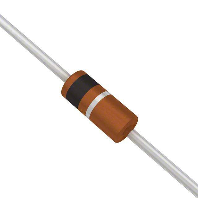
| 描述 | DIODE ZENER 500MW 5MA DO-35稳压二极管 3.3 Volt 0.5W 2% |
| 产品分类 | 单二极管/齐纳分离式半导体 |
| 品牌 | Vishay Semiconductor Diodes DivisionVishay Semiconductors |
| 产品手册 | |
| 产品图片 | |
| rohs | RoHS 合规性豁免无铅 / 符合限制有害物质指令(RoHS)规范要求 |
| 产品系列 | 二极管与整流器,稳压二极管,Vishay Semiconductors TZX3V3C-TR* |
| 数据手册 | |
| 产品型号 | TZX3V3C-TRTZX3V3C-TR |
| 产品 | Small Signal Zener Diodes |
| 产品种类 | |
| 功率耗散 | 500 mW |
| 商标 | Vishay Semiconductors |
| 安装风格 | Through Hole |
| 封装 | Reel |
| 封装/箱体 | DO-35 |
| 工厂包装数量 | 10000 |
| 最大反向漏泄电流 | 5 uA |
| 最大工作温度 | + 175 C |
| 最大齐纳阻抗 | 100 Ohms |
| 最小工作温度 | - 65 C |
| 标准包装 | 10,000 |
| 电压容差 | 2 % |
| 配置 | Single |
| 齐纳电压 | 3.3 V |
| 齐纳电流 | 5 mA |


- 商务部:美国ITC正式对集成电路等产品启动337调查
- 曝三星4nm工艺存在良率问题 高通将骁龙8 Gen1或转产台积电
- 太阳诱电将投资9.5亿元在常州建新厂生产MLCC 预计2023年完工
- 英特尔发布欧洲新工厂建设计划 深化IDM 2.0 战略
- 台积电先进制程称霸业界 有大客户加持明年业绩稳了
- 达到5530亿美元!SIA预计今年全球半导体销售额将创下新高
- 英特尔拟将自动驾驶子公司Mobileye上市 估值或超500亿美元
- 三星加码芯片和SET,合并消费电子和移动部门,撤换高东真等 CEO
- 三星电子宣布重大人事变动 还合并消费电子和移动部门
- 海关总署:前11个月进口集成电路产品价值2.52万亿元 增长14.8%


PDF Datasheet 数据手册内容提取
TZX-Series www.vishay.com Vishay Semiconductors Small Signal Zener Diodes FEATURES • Very sharp reverse characteristic • Low reverse current level • Very high stability • Low noise • AEC-Q101 qualified • Material categorization: For definitions of compliance please see www.vishay.com/doc?99912 APPLICATIONS • Voltage stabilization PRIMARY CHARACTERISTICS PARAMETER VALUE UNIT V range nom. 2.4 to 36 V Z Test current I 2; 5 mA ZT V specification Pulse current Z Int. construction Single ORDERING INFORMATION DEVICE NAME ORDERING CODE TAPED UNITS PER REEL MINIMUM ORDER QUANTITY 10 000 per ammopack TZX-series TZX-series-TAP 30 000/box (52 mm tape) 10 000 per 14" reel TZX-series TZX-series-TR 30 000/box (52 mm tape) PACKAGE MOLDING COMPOUND MOISTURE SENSITIVITY PACKAGE NAME WEIGHT SOLDERING CONDITIONS FLAMMABILITY RATING LEVEL MSL level 1 DO-35 125 mg UL 94 V-0 260 °C/10 s at terminals (according J-STD-020) ABSOLUTE MAXIMUM RATINGS (T = 25 °C, unless otherwise specified) amb PARAMETER TEST CONDITION SYMBOL VALUE UNIT Power dissipation l = 4 mm, T = 25 °C P 500 mW L tot Zener current I P /V mA Z tot Z Thermal resistance junction to ambient air l = 4 mm, T =constant R 300 K/W L thJA Junction temperature T 175 °C j Storage temperature range T - 65 to + 175 °C stg Forward voltage (max.) I = 200 mA V 1.5 V F F Rev. 2.4, 14-Apr-14 1 Document Number: 85614 For technical questions within your region: DiodesAmericas@vishay.com, DiodesAsia@vishay.com, DiodesEurope@vishay.com THIS DOCUMENT IS SUBJECT TO CHANGE WITHOUT NOTICE. THE PRODUCTS DESCRIBED HEREIN AND THIS DOCUMENT ARE SUBJECT TO SPECIFIC DISCLAIMERS, SET FORTH AT www.vishay.com/doc?91000
TZX-Series www.vishay.com Vishay Semiconductors ELECTRICAL CHARACTERISTICS (T = 25 °C, unless otherwise specified) amb ZENER VOLTAGE DYNAMIC TEST CURRENT REVERSE LEAKAGE CURRENT RANGE RESISTANCE PART NUMBER VZ at IZT1 IZT1 IR at VR IR at VR (1) ZZ at IZT1 V mA μA V μA V MIN. MAX. MAX. MAX. MAX. TZX2V4A 2.3 2.5 5 5 0.5 50 1 100 TZX2V4B 2.4 2.6 5 5 0.5 50 1 100 TZX2V7A 2.5 2.7 5 5 0.5 10 1 100 TZX2V7B 2.6 2.8 5 5 0.5 10 1 100 TZX2V7C 2.7 2.9 5 5 0.5 10 1 100 TZX3V0A 2.8 3 5 5 0.5 6 1 100 TZX3V0B 2.9 3.1 5 5 0.5 6 1 100 TZX3V0C 3 3.2 5 5 0.5 6 1 100 TZX3V3A 3.1 3.3 5 5 1 2 1 100 TZX3V3B 3.2 3.4 5 5 1 2 1 100 TZX3V3C 3.3 3.5 5 5 1 2 1 100 TZX3V6A 3.4 3.6 5 5 1 2 1 100 TZX3V6B 3.5 3.7 5 5 1 2 1 100 TZX3V6C 3.6 3.8 5 5 1 2 1 100 TZX3V9A 3.7 3.9 5 5 1 2 1 100 TZX3V9B 3.8 4 5 5 1 2 1 100 TZX3V9C 3.9 4.1 5 5 1 2 1 100 TZX4V3A 4 4.2 5 5 1.5 1 1 100 TZX4V3B 4.1 4.3 5 5 1.5 1 1 100 TZX4V3C 4.2 4.4 5 5 1.5 1 1 100 TZX4V3D 4.3 4.5 5 5 1.5 1 1 100 TZX4V7A 4.4 4.6 5 5 2 6 2 100 TZX4V7B 4.5 4.7 5 5 2 5 2 100 TZX4V7C 4.6 4.8 5 5 2 4 2 100 TZX4V7D 4.7 4.9 5 5 2 3 2 100 TZX5V1A 4.8 5 5 5 2 2 2 100 TZX5V1B 4.9 5.1 5 5 2 2 2 100 TZX5V1C 5 5.2 5 5 2 2 2 100 TZX5V1D 5.1 5.3 5 5 2 2 2 100 TZX5V6A 5.2 5.5 5 5 2 1 2 40 TZX5V6B 5.3 5.6 5 5 2 1 2 40 TZX5V6C 5.4 5.7 5 5 2 1 2 40 TZX5V6D 5.5 5.8 5 5 2 1 2 40 TZX5V6E 5.6 5.9 5 5 2 1 2 40 TZX6V2A 5.7 6 5 1 3 3 4 15 TZX6V2B 5.8 6.1 5 1 3 3 4 15 TZX6V2C 6 6.3 5 1 3 3 4 15 TZX6V2D 6.1 6.4 5 1 3 3 4 15 TZX6V2E 6.3 6.6 5 1 3 3 4 15 TZX6V8A 6.4 6.7 5 1 3.5 2 4 15 TZX6V8B 6.6 6.9 5 1 3.5 2 4 15 TZX6V8C 6.7 7 5 1 3.5 2 4 15 TZX6V8D 6.9 7.2 5 1 3.5 2 4 15 Rev. 2.4, 14-Apr-14 2 Document Number: 85614 For technical questions within your region: DiodesAmericas@vishay.com, DiodesAsia@vishay.com, DiodesEurope@vishay.com THIS DOCUMENT IS SUBJECT TO CHANGE WITHOUT NOTICE. THE PRODUCTS DESCRIBED HEREIN AND THIS DOCUMENT ARE SUBJECT TO SPECIFIC DISCLAIMERS, SET FORTH AT www.vishay.com/doc?91000
TZX-Series www.vishay.com Vishay Semiconductors ELECTRICAL CHARACTERISTICS (T = 25 °C, unless otherwise specified) amb ZENER VOLTAGE DYNAMIC TEST CURRENT REVERSE LEAKAGE CURRENT RANGE RESISTANCE PART NUMBER VZ at IZT1 IZT1 IR at VR IR at VR (1) ZZ at IZT1 V mA μA V μA V MIN. MAX. MAX. MAX. MAX. TZX7V5A 7 7.3 5 1 5 30 6.65 15 TZX7V5B 7.2 7.6 5 1 5 30 6.84 15 TZX7V5C 7.3 7.7 5 1 5 30 6.94 15 TZX7V5D 7.5 7.9 5 1 5 30 7.13 15 TZX7V5X 7.07 7.45 5 1 5 30 6.72 15 TZX8V2A 7.7 8.1 5 1 6.2 0.1 7.32 20 TZX8V2B 7.9 8.3 5 1 6.2 0.1 7.5 20 TZX8V2C 8.1 8.5 5 1 6.2 0.1 7.7 20 TZX8V2D 8.3 8.7 5 1 6.2 0.1 7.98 20 TZX9V1A 8.5 8.9 5 1 6.8 0.04 8.08 20 TZX9V1B 8.7 9.1 5 1 6.8 0.04 8.27 20 TZX9V1C 8.9 9.3 5 1 6.8 0.04 8.46 20 TZX9V1D 9.1 9.5 5 1 6.8 0.04 8.65 20 TZX9V1E 9.3 9.7 5 1 6.8 0.04 8.84 20 TZX10A 9.5 9.9 5 1 7.5 0.04 9.03 25 TZX10B 9.7 10.1 5 1 7.5 0.04 9.22 25 TZX10C 9.9 10.3 5 1 7.5 0.04 9.41 25 TZX10D 10.2 10.6 5 1 7.5 0.04 9.69 25 TZX11A 10.4 10.8 5 1 8.2 0.04 9.88 25 TZX11B 10.7 11.1 5 1 8.2 0.04 10.2 25 TZX11C 10.9 11.3 5 1 8.2 0.04 10.4 25 TZX11D 11.1 11.6 5 1 8.2 0.04 10.5 25 TZX12A 11.4 11.9 5 1 9.5 0.04 10.8 35 TZX12B 11.6 12.1 5 1 9.5 0.04 11 35 TZX12C 11.9 12.4 5 1 9.5 0.04 11.3 35 TZX12D 12.2 12.7 5 1 9.5 0.04 11.6 35 TZX12X 11.44 12.03 5 1 9.5 0.04 10.9 35 TZX13A 12.4 12.9 5 1 10 0.04 11.8 35 TZX13B 12.6 13.1 5 1 10 0.04 12 35 TZX13C 12.9 13.4 5 1 10 0.04 12.3 35 TZX14A 13.2 13.7 5 1 11 0.04 12.5 35 TZX14B 13.5 14 5 1 11 0.04 12.8 35 TZX14C 13.8 14.3 5 1 11 0.04 13.1 35 TZX15A 14.1 14.7 5 1 11.5 0.04 13.4 40 TZX15B 14.5 15.1 5 1 11.5 0.04 13.8 40 TZX15C 14.9 15.5 5 1 11.5 0.04 14.2 40 TZX15X 14.35 15.09 5 1 11.5 0.04 13.6 40 TZX16A 15.3 15.9 5 1 12 0.04 14.5 45 TZX16B 15.7 16.5 5 1 12 0.04 14.9 45 TZX16C 16.3 17.1 5 1 12 0.04 15.5 45 TZX18A 16.9 17.7 5 1 13 0.04 16.1 55 TZX18B 17.5 18.3 5 1 13 0.04 16.6 55 TZX18C 18.1 19 5 1 13 0.04 17.2 55 TZX20A 18.8 19.7 2 1 15 0.04 17.9 60 TZX20B 19.5 20.4 2 1 15 0.04 18.5 60 TZX20C 20.2 21.2 2 1 15 0.04 19.2 60 TZX22A 20.9 21.9 2 1 17 0.04 19.9 65 Rev. 2.4, 14-Apr-14 3 Document Number: 85614 For technical questions within your region: DiodesAmericas@vishay.com, DiodesAsia@vishay.com, DiodesEurope@vishay.com THIS DOCUMENT IS SUBJECT TO CHANGE WITHOUT NOTICE. THE PRODUCTS DESCRIBED HEREIN AND THIS DOCUMENT ARE SUBJECT TO SPECIFIC DISCLAIMERS, SET FORTH AT www.vishay.com/doc?91000
TZX-Series www.vishay.com Vishay Semiconductors ELECTRICAL CHARACTERISTICS (T = 25 °C, unless otherwise specified) amb ZENER VOLTAGE DYNAMIC TEST CURRENT REVERSE LEAKAGE CURRENT RANGE RESISTANCE PART NUMBER VZ at IZT1 IZT1 IR at VR IR at VR (1) ZZ at IZT1 V mA μA V μA V MIN. MAX. MAX. MAX. MAX. TZX22B 21.6 22.6 2 1 17 0.04 20.5 65 TZX22C 22.3 23.3 2 1 17 0.04 21.2 65 TZX24A 22.9 24 2 1 19 0.04 21.8 70 TZX24B 23.6 24.7 2 1 19 0.04 22.4 70 TZX24C 24.3 25.5 2 1 19 0.04 23.1 70 TZX24X 22.61 23.77 2 1 19 0.04 21.5 70 TZX27A 25.2 26.6 2 1 21 0.04 23.9 80 TZX27B 26.2 27.6 2 1 21 0.04 24.9 80 TZX27C 27.2 28.6 2 1 21 0.04 25.8 80 TZX27X 26.99 28.39 2 1 21 0.04 25.6 80 TZX30A 28.2 29.6 2 1 23 0.04 26.8 100 TZX30B 29.2 30.6 2 1 23 0.04 27.7 100 TZX30C 30.2 31.6 2 1 23 0.04 28.7 100 TZX30X 29.02 30.51 2 1 23 0.04 27.6 100 TZX33A 31.2 32.6 2 1 25 0.04 29.6 120 TZX33B 32.2 33.6 2 1 25 0.04 30.6 120 TZX33C 33.2 34.5 2 1 25 0.04 31.5 120 TZX36A 34.2 35.7 2 1 27 0.04 32.5 140 TZX36B 35.3 36.8 2 1 27 0.04 33.5 140 TZX36C 36.4 38 2 1 27 0.04 34.6 140 TZX36X 35.36 37.19 2 1 27 0.04 33.6 140 Notes • Additional measurement of voltage group TZM9V1 to TZX36, IR at 95 % VZmin. 40 nA at Tj = 25 °C (1) Additional measurement BASIC CHARACTERISTICS (T = 25 °C, unless otherwise specified) amb W) 500 600 K/ W) bient ( 400 on (m 500 m ati 400 A p Junction 300 l l wer Dissi 300 st. 200 Po 200 Therm. Resi 1000 TL = constant P - Total tot 1000 - A 0 5 10 15 20 0 40 80 120 160 200 RthJ I - Lead Length (mm) 95 9611 95 9602 Tamb - Ambient Temperature (°C) Fig. 1 - Thermal Resistance vs. Lead Length Fig. 2 - Total Power Dissipation vs. Ambient Temperature Rev. 2.4, 14-Apr-14 4 Document Number: 85614 For technical questions within your region: DiodesAmericas@vishay.com, DiodesAsia@vishay.com, DiodesEurope@vishay.com THIS DOCUMENT IS SUBJECT TO CHANGE WITHOUT NOTICE. THE PRODUCTS DESCRIBED HEREIN AND THIS DOCUMENT ARE SUBJECT TO SPECIFIC DISCLAIMERS, SET FORTH AT www.vishay.com/doc?91000
TZX-Series www.vishay.com Vishay Semiconductors 1000 200 V) pF) ge (m 100 ance ( 150 VR = 2 V han acit Tj = 25 °C C p 100 oltage 10 IZ = 5 mA ode Ca V - VZ - DiD 50 C 1 0 0 5 10 15 20 25 0 5 10 15 20 25 95 9598 VZ - Z-Voltage (V) 95 9601 VZ - Z-Voltage (V) Fig. 3 - Typical Change of Working Voltage under Operating Fig. 6 - Diode Capacitance vs. Z-Voltage Conditions at T = 25 °C amb 1.3 100 e VZtn = VZt/VZ (25 °C) oltage Chang 11..12 TKVZ = 10 x 10-4/K 846 xxx 111000---444///KKK Current (mA) 101 Tj = 25 °C ve V 1.0 20 x 10-4/K ard 0.1 - RelatiZtn 0.9 -- 42 xx 1100--44//KK I - ForwF 0.01 V 0.8 0.001 - 60 0 60 120 180 240 0 0.2 0.4 0.6 0.8 1.0 95 9599 Tj - Junction Temperature (°C) 959605 VF - Forward Voltage (V) Fig. 4 - Typical Change of Working Voltage vs. Fig. 7 - Forward Current vs. Forward Voltage Junction Temperature 100 15 nt e 80 oeffici 10 mA) PTtaomt =b =5 0205 m°CW perature C-4V (10/K)Z 5 Z-Current ( 4600 emof IZ = 5 mA - Z - TZ 0 I 20 V K T 0 - 5 0 4 6 8 12 20 0 10 20 30 40 50 95 9604 VZ - Z-Voltage (V) 95 9600 VZ - Z-Voltage (V) Fig. 8 - Z-Current vs. Z-Voltage Fig. 5 - Temperature Coefficient of Vz vs. Z-Voltage Rev. 2.4, 14-Apr-14 5 Document Number: 85614 For technical questions within your region: DiodesAmericas@vishay.com, DiodesAsia@vishay.com, DiodesEurope@vishay.com THIS DOCUMENT IS SUBJECT TO CHANGE WITHOUT NOTICE. THE PRODUCTS DESCRIBED HEREIN AND THIS DOCUMENT ARE SUBJECT TO SPECIFIC DISCLAIMERS, SET FORTH AT www.vishay.com/doc?91000
TZX-Series www.vishay.com Vishay Semiconductors 50 1000 Ω) A) 40 PTtaomt =b =5 0205 m°CW ance ( IZ = 1 mA m st 100 nt ( 30 Resi Z-Curre 20 ntial Z- 10 105 mmAA - Z ere I 10 Diff 0 r - Z 1 Tj = 25 °C 15 20 25 30 35 0 5 10 15 20 25 95 9607 VZ - Z-Voltage (V) 95 9606 VZ - Z-Voltage (V) Fig. 9 - Z-Current vs. Z-Voltage Fig. 10 - Differential Z-Resistance vs. Z-Voltage W) K/ 1000 d. ( n o e C tp/T = 0.5 or Puls 100 tp/T = 0.2 e f Single Pulse R = 300 K/W c thJA sistan 10 tp/T = 0.01 T = Tj max. - Tamb Re tp/T = 0.1 tp/T = 0.02 ermal tp/T = 0.05 iZM = (- VZ + (VZ2 + 4rzj x T/Zthp) 1/2)/(2rzj) Th 1 Z - thp 10-1 100 t - Pulse Leng1t0h1 (ms) 102 95 9603 p Fig. 11 - Thermal Response PACKAGE DIMENSIONS in millimeters (inches): DO-35 Cathode Identification Ø 0.6 max. [0.024] Ø 0.4 min. [0.015] 26 min. [1.024] 33..91 mmainx.. [[00..112504]] 26 min. [1.024] 1.7 [0.067] 1.3 [0.050] Rev. 6 - Date: 19. December 2011 Document no.: SB-V-3906.04-031(4) 94 9366 Rev. 2.4, 14-Apr-14 6 Document Number: 85614 For technical questions within your region: DiodesAmericas@vishay.com, DiodesAsia@vishay.com, DiodesEurope@vishay.com THIS DOCUMENT IS SUBJECT TO CHANGE WITHOUT NOTICE. THE PRODUCTS DESCRIBED HEREIN AND THIS DOCUMENT ARE SUBJECT TO SPECIFIC DISCLAIMERS, SET FORTH AT www.vishay.com/doc?91000
Legal Disclaimer Notice www.vishay.com Vishay Disclaimer ALL PRODUCT, PRODUCT SPECIFICATIONS AND DATA ARE SUBJECT TO CHANGE WITHOUT NOTICE TO IMPROVE RELIABILITY, FUNCTION OR DESIGN OR OTHERWISE. Vishay Intertechnology, Inc., its affiliates, agents, and employees, and all persons acting on its or their behalf (collectively, “Vishay”), disclaim any and all liability for any errors, inaccuracies or incompleteness contained in any datasheet or in any other disclosure relating to any product. Vishay makes no warranty, representation or guarantee regarding the suitability of the products for any particular purpose or the continuing production of any product. To the maximum extent permitted by applicable law, Vishay disclaims (i) any and all liability arising out of the application or use of any product, (ii) any and all liability, including without limitation special, consequential or incidental damages, and (iii) any and all implied warranties, including warranties of fitness for particular purpose, non-infringement and merchantability. Statements regarding the suitability of products for certain types of applications are based on Vishay’s knowledge of typical requirements that are often placed on Vishay products in generic applications. Such statements are not binding statements about the suitability of products for a particular application. It is the customer’s responsibility to validate that a particular product with the properties described in the product specification is suitable for use in a particular application. Parameters provided in datasheets and / or specifications may vary in different applications and performance may vary over time. All operating parameters, including typical parameters, must be validated for each customer application by the customer’s technical experts. Product specifications do not expand or otherwise modify Vishay’s terms and conditions of purchase, including but not limited to the warranty expressed therein. Except as expressly indicated in writing, Vishay products are not designed for use in medical, life-saving, or life-sustaining applications or for any other application in which the failure of the Vishay product could result in personal injury or death. Customers using or selling Vishay products not expressly indicated for use in such applications do so at their own risk. Please contact authorized Vishay personnel to obtain written terms and conditions regarding products designed for such applications. No license, express or implied, by estoppel or otherwise, to any intellectual property rights is granted by this document or by any conduct of Vishay. Product names and markings noted herein may be trademarks of their respective owners. © 2017 VISHAY INTERTECHNOLOGY, INC. ALL RIGHTS RESERVED Revision: 08-Feb-17 1 Document Number: 91000
Mouser Electronics Authorized Distributor Click to View Pricing, Inventory, Delivery & Lifecycle Information: V ishay: TZX2V4B-TAP TZX33A-TAP TZX13A-TAP TZX8V2A-TAP TZX22C-TAP TZX12C-TAP TZX6V2A-TAP TZX7V5C- TAP TZX11A-TAP TZX6V8B-TAP TZX3V0C-TAP TZX4V7A-TAP TZX2V7A-TAP TZX5V1A-TAP TZX9V1A-TAP TZX12B-TAP TZX22B-TAP TZX14A-TAP TZX24A-TAP TZX27A-TAP TZX6V8A-TAP TZX3V3C-TAP TZX6V8D- TAP TZX15B-TAP TZX5V6E-TAP TZX27C-TAP TZX5V6B-TAP TZX14B-TAP TZX33B-TAP TZX13B-TAP TZX24B-TAP TZX36A-TAP TZX16A-TAP TZX6V2E-TAP TZX3V6B-TAP TZX7V5D-TAP TZX3V9A-TAP TZX5V6D- TAP TZX6V8C-TAP TZX15C-TAP TZX20B-TAP TZX30B-TAP TZX10B-TAP TZX11D-TAP TZX6V2B-TAP TZX7V5A-TAP TZX22A-TAP TZX12A-TAP TZX3V0B-TAP TZX8V2B-TAP TZX2V7C-TAP TZX9V1B-TAP TZX5V1D-TAP TZX4V7B-TAP TZX5V1B-TAP TZX15A-TAP TZX9V1C-TAP TZX11C-TAP TZX6V2C-TAP TZX9V1D-TAP TZX2V7B-TAP TZX8V2C-TAP TZX27B-TAP TZX16C-TAP TZX36C-TAP TZX20A-TAP TZX30A- TAP TZX10A-TAP TZX3V0A-TAP TZX16B-TAP TZX36B-TAP TZX3V6C-TAP TZX18C-TAP TZX4V3A-TAP TZX5V6C-TAP TZX33C-TAP TZX13C-TAP TZX12D-TAP TZX3V3A-TAP TZX4V7D-TAP TZX18B-TAP TZX11B- TAP TZX9V1E-TAP TZX3V3B-TAP TZX14C-TAP TZX24C-TAP TZX3V9B-TAP TZX18A-TAP TZX20C-TAP TZX10C-TAP TZX4V3B-TAP TZX4V3D-TAP TZX2V4A-TAP TZX5V6A-TAP TZX30C-TAP TZX3V9C-TAP TZX10D- TAP TZX3V6A-TAP TZX8V2D-TAP TZX7V5B-TAP