ICGOO在线商城 > 集成电路(IC) > 逻辑器件 - 转换器,电平移位器 > TXS0206AYFPR
- 型号: TXS0206AYFPR
- 制造商: Texas Instruments
- 库位|库存: xxxx|xxxx
- 要求:
| 数量阶梯 | 香港交货 | 国内含税 |
| +xxxx | $xxxx | ¥xxxx |
查看当月历史价格
查看今年历史价格
TXS0206AYFPR产品简介:
ICGOO电子元器件商城为您提供TXS0206AYFPR由Texas Instruments设计生产,在icgoo商城现货销售,并且可以通过原厂、代理商等渠道进行代购。 TXS0206AYFPR价格参考¥3.67-¥8.22。Texas InstrumentsTXS0206AYFPR封装/规格:逻辑器件 - 转换器,电平移位器, Voltage Level Translator Bidirectional 1 Circuit 4 Channel 60Mbps 20-DSBGA。您可以下载TXS0206AYFPR参考资料、Datasheet数据手册功能说明书,资料中有TXS0206AYFPR 详细功能的应用电路图电压和使用方法及教程。
| 参数 | 数值 |
| 产品目录 | 集成电路 (IC) |
| 描述 | IC V-LEVEL TRANSL MMC/SD 20DSBGA |
| 产品分类 | 逻辑 - 变换器 |
| 品牌 | Texas Instruments |
| 数据手册 | |
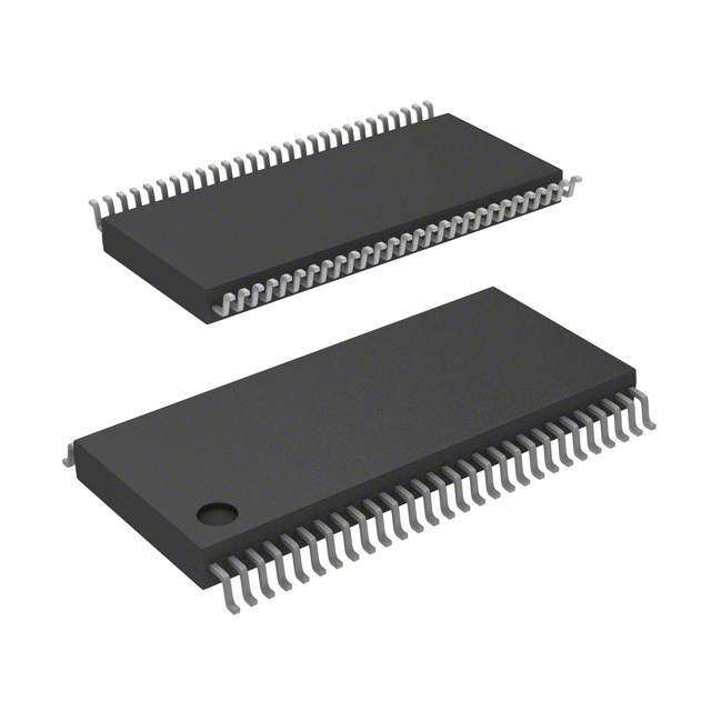
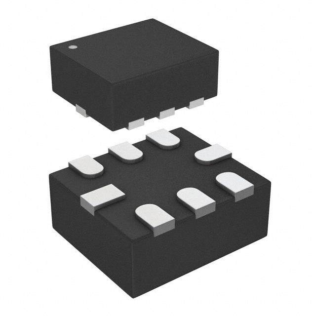
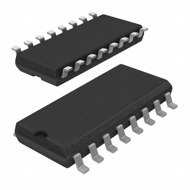
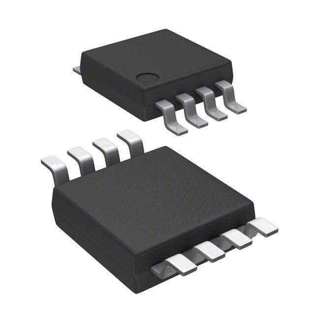
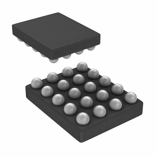
| 产品图片 |
|
| 产品型号 | TXS0206AYFPR |
| rohs | 无铅 / 符合限制有害物质指令(RoHS)规范要求 |
| 产品系列 | - |
| 传播延迟(最大值) | 3.2ns |
| 位数 | 4 |
| 供应商器件封装 | 20-DSBGA(1.96x1.56) |
| 其它名称 | 296-36872-1 |
| 包装 | 剪切带 (CT) |
| 安装类型 | 表面贴装 |
| 封装/外壳 | 20-XFBGA,DSBGA |
| 工作温度 | -40°C ~ 85°C |
| 差分-输入:输出 | 无/无 |
| 数据速率 | 60Mbps |
| 标准包装 | 1 |
| 电压-电源 | 1.1 V ~ 3.6 V |
| 输入类型 | 电压 |
| 输出/通道数 | 1 |
| 输出类型 | 电压 |
| 通道数 | 4 |
| 逻辑功能 | 变换器 |






- 商务部:美国ITC正式对集成电路等产品启动337调查
- 曝三星4nm工艺存在良率问题 高通将骁龙8 Gen1或转产台积电
- 太阳诱电将投资9.5亿元在常州建新厂生产MLCC 预计2023年完工
- 英特尔发布欧洲新工厂建设计划 深化IDM 2.0 战略
- 台积电先进制程称霸业界 有大客户加持明年业绩稳了
- 达到5530亿美元!SIA预计今年全球半导体销售额将创下新高
- 英特尔拟将自动驾驶子公司Mobileye上市 估值或超500亿美元
- 三星加码芯片和SET,合并消费电子和移动部门,撤换高东真等 CEO
- 三星电子宣布重大人事变动 还合并消费电子和移动部门
- 海关总署:前11个月进口集成电路产品价值2.52万亿元 增长14.8%


PDF Datasheet 数据手册内容提取
Product Sample & Technical Tools & Support & Folder Buy Documents Software Community TXS0206A SCES833B–NOVEMBER2011–REVISEDAPRIL2016 TXS0206A SD Card Voltage-Translation Transceiver 1 Features 3 Description • LevelTranslator The TXS0206A is a level shifter for interfacing 1 microprocessors with MultiMediaCards (MMCs), – V andV Rangeof1.1Vto3.6V CCA CCB securedigital(SD)cards,andMemoryStick™cards. – FastPropagationDelay(4.4nsMaximum The voltage-level translator has two supply voltage WhenTranslatingBetween1.8Vand3V) pins. V as well as V can be operated over the CCA CCB • ESDProtectionExceedsJESD22 full range of 1.1 V to 3.6 V. The TXS0206A enables – 2500-VHuman-BodyModel(A114-B) system designers to easily interface applications processorsordigitalbasebandstomemorycardsand – 250-VMachineModel(A115-A) SDIO peripherals operating at a different I/O voltage – 1500-VCharged-DeviceModel(C101) level. 2 Applications The TXS0206A is offered in a 20-bump wafer chip scale package (WCSP). This package has • MobilePhones dimensions of 1.96 mm × 1.56 mm, with a 0.4-mm • TabletPCs ball pitch for effective board-space savings. Memory cardsarewidelyusedinmobilephones,PDAs,digital • Notebooks cameras, personal media players, camcorders, set- • UltrabookComputers top boxes, etc. Low static power consumption and small package size make the TXS0206A an ideal choicefortheseapplications. DeviceInformation(1) PARTNUMBER PACKAGE BODYSIZE TXS0206A DSBGA(20) 1.96mm×1.56mm (1) For all available packages, see the orderable addendum at theendofthedatasheet. ApplicationExample 8 7 SD/MMC 6 TXS0206A 5 SD/MMC 4 Controller 3 Card 2 1 9 1 An IMPORTANT NOTICE at the end of this data sheet addresses availability, warranty, changes, use in safety-critical applications, intellectualpropertymattersandotherimportantdisclaimers.PRODUCTIONDATA.
TXS0206A SCES833B–NOVEMBER2011–REVISEDAPRIL2016 www.ti.com Table of Contents 1 Features.................................................................. 1 7 ParameterMeasurementInformation................15 2 Applications........................................................... 1 8 DetailedDescription............................................ 16 3 Description............................................................. 1 8.1 Overview.................................................................16 4 RevisionHistory..................................................... 2 8.2 FunctionalBlockDiagram.......................................16 5 PinConfigurationandFunctions......................... 3 8.3 FeatureDescription.................................................17 8.4 DeviceFunctionalModes........................................18 6 Specifications......................................................... 4 9 ApplicationandImplementation........................ 19 6.1 AbsoluteMaximumRatings......................................4 6.2 ESDRatings ............................................................4 9.1 ApplicationInformation............................................19 6.3 RecommendedOperatingConditions.......................5 9.2 TypicalApplication .................................................19 6.4 ThermalInformation..................................................6 9.3 SystemExamples...................................................21 6.5 ElectricalCharacteristics...........................................6 10 PowerSupplyRecommendations..................... 22 6.6 TimingRequirements—V =1.2V±0.1V...........7 11 Layout................................................................... 22 CCA 6.7 TimingRequirements—V =1.8V±0.15V.........8 11.1 LayoutGuidelines.................................................22 CCA 6.8 TimingRequirements—V =3.3V±0.3V...........8 11.2 LayoutExample....................................................23 CCA 6.9 SwitchingCharacteristics—V =1.2V±0.1V ....9 12 DeviceandDocumentationSupport................. 24 CCA 6.10 SwitchingCharacteristics—V =1.8V±0.15V 12.1 DocumentationSupport .......................................24 CCA ................................................................................. 10 12.2 CommunityResources..........................................24 6.11 SwitchingCharacteristics—VCCA=3.3V±0.3V.11 12.3 Trademarks...........................................................24 6.12 OperatingCharacteristics—VCCA=1.2V............12 12.4 ElectrostaticDischargeCaution............................24 6.13 OperatingCharacteristics—VCCA=1.8V............13 12.5 Glossary................................................................24 6.14 OperatingCharacteristics—VCCA=3.3V...........13 13 Mechanical,Packaging,andOrderable 6.15 TypicalCharacteristics..........................................14 Information........................................................... 24 4 Revision History NOTE:Pagenumbersforpreviousrevisionsmaydifferfrompagenumbersinthecurrentversion. ChangesfromRevisionA(May2012)toRevisionB Page • AddedDeviceInformationtable,ESDRatingstable,FeatureDescriptionsection,DeviceFunctionalModes, ApplicationandImplementationsection,PowerSupplyRecommendationssection,Layoutsection,Deviceand DocumentationSupportsection,andMechanical,Packaging,andOrderableInformationsection. .................................... 1 • Deletedtheorderinginformation.SeePOAattheendofthedatasheet............................................................................... 1 2 SubmitDocumentationFeedback Copyright©2011–2016,TexasInstrumentsIncorporated ProductFolderLinks:TXS0206A
TXS0206A www.ti.com SCES833B–NOVEMBER2011–REVISEDAPRIL2016 5 Pin Configuration and Functions YFPPackage 20–PinDSBGA TopView 1 2 3 4 A B C D E PinAssignments 1 2 3 4 A DAT2A V WP DAT2B CCA B DAT3A CD V DAT3B CCB C CMDA GND GND CMDB D DAT0A CLKA CLKB DAT0B E DAT1A CLK-f EN DAT1B PinFunctions PIN TYPE DESCRIPTION NO. NAME A1 DAT2A I/O Databit2connectedtohost.ReferencedtoV .Includesa40-kΩpullupresistortoV CCA CCA. A2 V Pwr A-portsupplyvoltage.V powersallA-portI/Osandcontrolinputs. CCA CCA Connectedtowriteprotectonthemechanicalconnector.TheWPpinhasaninternal100-kΩ(±30%) A3 WP O pullupresistortoV .Leaveunconnectedifnotused. CCA A4 DAT2B I/O Databit2connectedtomemorycard.ReferencedtoV .Includesa40-kΩpullupresistortoV . CCB CCB B1 DAT3A I/O Databit3connectedtohost.ReferencedtoV .Includesa40-kΩpullupresistortoV . CCA CCA Connectedtocarddetectonthemechanicalconnector.TheCDpinhasaninternal100-kΩ(±30%) B2 CD O pullupresistortoV .Leaveunconnectedifnotused. CCA B3 V Pwr B-portsupplyvoltage.V powersallB-portI/Os. CCB CCB B4 DAT3B I/O Databit3connectedtomemorycard.ReferencedtoV .Includesa40-kΩpullupresistortoV . CCB CCB C1 CMDA I/O Commandbitconnectedtohost.ReferencedtoV .Includesa40-kΩpullupresistortoV . CCA CCA C2 GND — Ground C3 GND — Ground C4 CMDB I/O Commandbitconnectedtomemorycard.ReferencedtoV .Includesa40-kΩpullupresistortoV . CCB CCB D1 DAT0A I/O Databit0connectedtohost.ReferencedtoV .Includesa40-kΩpullupresistortoV . CCA CCA D2 CLKA I Clocksignalconnectedtohost.ReferencedtoV . CCA D3 CLKB O Clocksignalconnectedtomemorycard.ReferencedtoV . CCB D4 DAT0B I/O Databit0connectedtomemorycard.ReferencedtoV .Includesa40-kΩpullupresistortoV . CCB CCB E1 DAT1A I/O Databit1connectedtohost.ReferencedtoV .Includesa40-kΩpullupresistortoV . CCA CCA E2 CLK-f O Clockfeedbacktohostforresynchronizingdatatoaprocessor.Leaveunconnectedifnotused. E3 EN I Enable/disablecontrol.PullENlowtoplacealloutputsinHi-Zstate.ReferencedtoV . CCA E4 DAT1B I/O Databit1connectedtomemorycard.ReferencedtoV .Includesa40-kΩpullupresistortoV . CCB CCB Copyright©2011–2016,TexasInstrumentsIncorporated SubmitDocumentationFeedback 3 ProductFolderLinks:TXS0206A
TXS0206A SCES833B–NOVEMBER2011–REVISEDAPRIL2016 www.ti.com 6 Specifications 6.1 Absolute Maximum Ratings overoperatingfree-airtemperaturerange(unlessotherwisenoted)(1) MIN MAX UNIT V Supplyvoltage,A-Port –0.5 4.6 V CCA V Supplyvoltage,B-Port –0.5 4.6 V CCB I/Oports(Aport) –0.5 4.6 V Inputvoltage I/Oports(Bport) –0.5 4.6 V I Controlinputs –0.5 4.6 Voltagerangeappliedtoanyoutputinthehigh-impedanceorpower-off Aport –0.5 4.6 V V O state Bport –0.5 4.6 Aport –0.5 4.6 V Voltagerangeappliedtoanyoutputinthehighorlowstate V O Bport –0.5 4.6 I Inputclampcurrent V <0 –50 mA IK I I Outputclampcurrent V <0 –50 mA OK O I Continuousoutputcurrent ±50 mA O ContinuouscurrentthroughV orGND ±100 mA CCA T Storagetemperature –65 150 °C stg (1) StressesbeyondthoselistedunderAbsoluteMaximumRatingsmaycausepermanentdamagetothedevice.Thesearestressratings only,whichdonotimplyfunctionaloperationofthedeviceattheseoranyotherconditionsbeyondthoseindicatedunderRecommended OperatingConditions.Exposuretoabsolute-maximum-ratedconditionsforextendedperiodsmayaffectdevicereliability. 6.2 ESD Ratings VALUE UNIT Human-bodymodel(HBM),perANSI/ESDA/JEDECJS-001(1) ±2500 Charged-devicemodel(CDM),perJEDECspecificationJESD22- V(ESD) Electrostaticdischarge C101(2) ±1500 V Machinemodel(MM) ±250 (1) JEDECdocumentJEP155statesthat500-VHBMallowssafemanufacturingwithastandardESDcontrolprocess. (2) JEDECdocumentJEP157statesthat250-VCDMallowssafemanufacturingwithastandardESDcontrolprocess. 4 SubmitDocumentationFeedback Copyright©2011–2016,TexasInstrumentsIncorporated ProductFolderLinks:TXS0206A
TXS0206A www.ti.com SCES833B–NOVEMBER2011–REVISEDAPRIL2016 6.3 Recommended Operating Conditions See(1) V V MIN MAX UNIT CCA CCB V Supplyvoltage 1.1 3.6 V CCA V Supplyvoltage 1.1 3.6 V CCB A-PortCMDand 1.1Vto1.95V 1.1Vto1.95V DATAI/Os V High-levelinput B-PortCMDand 1.95Vto3.6V 1.95Vto3.6V VCCI –0.2 VCCI V IH voltage DATAI/Os ENandCLKA 1.1Vto3.6V 1.1Vto3.6V V ×0.65 V CCI CCI A-PortCMDand 1.1Vto1.95V 1.1Vto1.95V DATAI/Os V Low-levelinput B-PortCMDand 1.95Vto3.6V 1.95Vto3.6V 0 0.15 V IL voltage DATAI/Os ENandCLKA 1.1Vto3.6V 1.1Vto3.6V 0 V ×0.35 CCI Activestate 0 V CCO V Outputvoltage V O 3-state 0 3.6 1.1Vto3.6V –100 µA 1.1Vto1.3V –0.5 1.4Vto1.6V –1 I High-leveloutputcurrent(CLK-foutput) 1.1Vto3.6V OH 1.65Vto1.95V –2 mA 2.3Vto2.7V –4 3Vto3.6V –8 1.1Vto3.6V 100 μA 1.1Vto1.3V 0.5 1.4Vto1.6V 1 I Low-leveloutputcurrent(CLK-foutput) 1.1Vto3.6V OL 1.65Vto1.95V 2 mA 2.3Vto2.7V 4 3Vto3.6V 8 1.1Vto3.6V –100 μA 1.1Vto1.3V –0.5 1.4Vto1.6V –1 I High-leveloutputcurrent(CLKoutput) 1.1Vto3.6V OH 1.65Vto1.95V –2 mA 2.3Vto2.7V –4 3Vto3.6V –8 1.1Vto3.6V 100 µA 1.1Vto1.3V 0.5 1.4Vto1.6V 1 I Low-leveloutputcurrent(CLKoutput) 1.1Vto3.6V OL 1.65Vto1.95V 2 mA 2.3Vto2.7V 4 3Vto3.6V 8 Δt/Δv Inputtransitionriseorfallrate 5 ns/V T Operatingfree-airtemperature –40 85 °C A (1) AllunuseddatainputsofthedevicemustbeheldatV orGNDtoensureproperdeviceoperation.RefertotheTIapplicationreport, CCI ImplicationsofSloworFloatingCMOSInputs,SCBA004. Copyright©2011–2016,TexasInstrumentsIncorporated SubmitDocumentationFeedback 5 ProductFolderLinks:TXS0206A
TXS0206A SCES833B–NOVEMBER2011–REVISEDAPRIL2016 www.ti.com 6.4 Thermal Information TXS0206A THERMALMETRIC(1) YFP(DSBGA) UNIT 20PINS R Junction-to-ambientthermalresistance 71.1 °C/W θJA R Junction-to-case(top)thermalresistance 0.5 °C/W θJC(top) R Junction-to-boardthermalresistance 10.4 °C/W θJB ψ Junction-to-topcharacterizationparameter 2 °C/W JT ψ Junction-to-boardcharacterizationparameter 10.4 °C/W JB (1) Formoreinformationabouttraditionalandnewthermalmetrics,seetheSemiconductorandICPackageThermalMetricsapplication report,SPRA953. 6.5 Electrical Characteristics overrecommendedoperatingfree-airtemperaturerange(unlessotherwisenoted) PARAMETER TESTCONDITIONS V V MIN TYP(1) MAX UNIT CCA CCB I =–100μA 1.1Vto3.6V 1.65Vto3.6V V ×0.8 OH CCA I =–0.5mA 1.1V 1.65Vto3.6V 0.8 OH Aport IOH=–1mA 1.4V 1.65Vto3.6V 1.05 (CLK-foutput) I =–2mA 1.65V 1.65Vto3.6V 1.2 OH V V OH I =–4mA 2.3V 1.65Vto3.6V 1.75 OH I =–8mA 3V 1.65Vto3.6V 2.3 OH Aport (DATandCMD I =–20μA 1.1Vto3.6V 1.65Vto3.6V V ×0.8 OH CCA outputs) I =100μA 1.1Vto3.6V 1.65Vto3.6V V ×0.2 OL CCA I =0.5mA 1.1V 1.65Vto3.6V 0.35 OL Aport IOL=1mA 1.4V 1.65Vto3.6V 0.35 V (CLK-foutput) I =2mA 1.65V 1.65Vto3.6V 0.45 OL I =4mA 2.3V 1.65Vto3.6V 0.55 OL V I =8mA 3V 1.65Vto3.6V 0.7 OL OL I =135μA 1.1V 1.65Vto3.6V 0.4 OL I =180μA 1.4V 1.65Vto3.6V 0.4 Aport OL (DATandCMD I =220μA 1.65V 1.65Vto3.6V 0.4 V OL outputs) I =300μA 2.3V 1.65Vto3.6V 0.4 OL I =400μA 3V 1.65Vto3.6V 0.55 OL I =–100μA 1.1Vto3.6V 1.65Vto3.6V V ×0.8 OH CCB Bport IOH=–2mA 1.1Vto3.6V 1.65V 1.2 (CLKoutput) I =–4mA 1.1Vto3.6V 2.3V 1.75 V OH V OH I =–8mA 1.1Vto3.6V 3V 2.3 OH Bport I =–20μA 1.1Vto3.6V 1.65Vto3.6V V ×0.8 (DAToutput) OH CCB (1) AlltypicalvaluesareatT =25°C. A 6 SubmitDocumentationFeedback Copyright©2011–2016,TexasInstrumentsIncorporated ProductFolderLinks:TXS0206A
TXS0206A www.ti.com SCES833B–NOVEMBER2011–REVISEDAPRIL2016 Electrical Characteristics (continued) overrecommendedoperatingfree-airtemperaturerange(unlessotherwisenoted) PARAMETER TESTCONDITIONS V V MIN TYP(1) MAX UNIT CCA CCB I =100μA 1.1Vto3.6V 1.65Vto3.6V V ×0.2 OL CCB I =2mA 1.1Vto3.6V 1.65V 0.45 OL Bport V I =4mA 1.1Vto3.6V 2.3V 0.55 OL I =8mA 1.1Vto3.6V 3V 0.7 OL V OL I =135μA 1.1Vto3.6V 1.65Vto3.6V 0.4 OL Bport IOL=220μA 1.1Vto3.6V 1.65V 0.4 V (DAToutput) I =300μA 1.1Vto3.6V 2.3V 0.4 OL I =300μA 1.1Vto3.6V 3V 0.55 OL I Controlinputs V =V orGND 1.1Vto3.6V 1.65Vto3.6V ±1 μA I I CCA I Aport V =V ,I =0 1.1Vto3.6V 1.65Vto3.6V 7 μA CCA I CCI O I Bport V =V ,I =0 1.1Vto3.6V 1.65Vto3.6V 11 μA CCB I CCI O Aport 5.5 6.5 C pF io Bport 7 9.5 Controlinputs V =V orGND 3.5 4.5 I CCA C pF i Clockinput V =V orGND 3 4 I CCA 6.6 Timing Requirements—V = 1.2 V ± 0.1 V CCA overrecommendedoperatingfree-airtemperaturerange(unlessotherwisenoted) V MIN MAX UNIT CC Push-pull VCCB=1.8V±0.15V 40 driving V =3.3V±0.3V 40 CCB Command Mbps Open-drain VCCB=1.8V±0.15V 1 driving V =3.3V±0.3V 1 CCB Datarate V =1.8V±0.15V 40 CCB Clock MHz Push-pull VCCB=3.3V±0.3V 40 driving V =1.8V±0.15V 40 CCB Data Mbps V =3.3V±0.3V 40 CCB Push-pull VCCB=1.8V±0.15V 25 ns driving V =3.3V±0.3V 25 CCB Command Open-drain VCCB=1.8V±0.15V 1 µs Pulse driving VCCB=3.3V±0.3V 1 t W duration V =1.8V±0.15V 10 CCB Clock ns Push-pull VCCB=3.3V±0.3V 8.3 driving V =1.8V±0.15V 25 CCB Data ns V =3.3V±0.3V 25 CCB Copyright©2011–2016,TexasInstrumentsIncorporated SubmitDocumentationFeedback 7 ProductFolderLinks:TXS0206A
TXS0206A SCES833B–NOVEMBER2011–REVISEDAPRIL2016 www.ti.com 6.7 Timing Requirements—V = 1.8 V ± 0.15 V CCA overrecommendedoperatingfree-airtemperaturerange(unlessotherwisenoted) V MIN MAX UNIT CC Push-pull VCCB=1.8V±0.15V 60 driving V =3.3V±0.3V 60 CCB Command Mbps Open-drain VCCB=1.8V±0.15V 1 driving V =3.3V±0.3V 1 CCB Datarate V =1.8V±0.15V 60 CCB Clock MHz Push-pull VCCB=3.3V±0.3V 60 driving V =1.8V±0.15V 60 CCB Data Mbps V =3.3V±0.3V 60 CCB Push-pull VCCB=1.8V±0.15V 17 ns driving V =3.3V±0.3V 17 CCB Command Open-drain VCCB=1.8V±0.15V 1 µs Pulse driving VCCB=3.3V±0.3V 1 t W duration V =1.8V±0.15V 8.3 CCB Clock ns Push-pull VCCB=3.3V±0.3V 8.3 driving V =1.8V±0.15V 17 CCB Data ns V =3.3V±0.3V 17 CCB 6.8 Timing Requirements—V = 3.3 V ± 0.3 V CCA overrecommendedoperatingfree-airtemperaturerange(unlessotherwisenoted) V MIN MAX UNIT CC Push-pull VCCB=1.8V±0.15V 60 driving V =3.3V±0.3V 60 CCB Command Mbps Open-drain VCCB=1.8V±0.15V 1 driving V =3.3V±0.3V 1 CCB Datarate V =1.8V±0.15V 55 CCB Clock MHz Push-pull VCCB=3.3V±0.3V 55 driving V =1.8V±0.15V 60 CCB Data Mbps V =3.3V±0.3V 60 CCB Push-pull VCCB=1.8V±0.15V 17 ns driving V =3.3V±0.3V 17 CCB Command Open-drain VCCB=1.8V±0.15V 1 µs Pulse driving VCCB=3.3V±0.3V 1 t W duration V =1.8V±0.15V 9 CCB Clock ns Push-pull VCCB=3.3V±0.3V 9 driving V =1.8V±0.15V 17 CCB Data ns V =3.3V±0.3V 17 CCB 8 SubmitDocumentationFeedback Copyright©2011–2016,TexasInstrumentsIncorporated ProductFolderLinks:TXS0206A
TXS0206A www.ti.com SCES833B–NOVEMBER2011–REVISEDAPRIL2016 6.9 Switching Characteristics—V = 1.2 V ± 0.1 V CCA overoperatingfree-airtemperaturerange(unlessotherwisenoted) FROM TO PARAMETER (INPUT) (OUTPUT) VCC MIN MAX UNIT VCCB=1.8V±0.15V 5.7 CMDA CMDB VCCB=3.3V±0.3V 4.4 VCCB=1.8V±0.15V 6.7 CMDB CMDA VCCB=3.3V±0.3V 5.8 VCCB=1.8V±0.15V 6.2 CLKA CLKB VCCB=3.3V±0.3V 4.5 tpd ns VCCB=1.8V±0.15V 7.6 DATxA DATxB VCCB=3.3V±0.3V 7.5 VCCB=1.8V±0.15V 6.3 DATxB DATxA VCCB=3.3V±0.3V 4.6 VCCB=1.8V±0.15V 12 CLKA CLK-f VCCB=3.3V±0.3V 7.9 VCCB=1.8V±0.15V 1 EN B-port VCCB=3.3V±0.3V 1 ten µs VCCB=1.8V±0.15V 1 EN A-port VCCB=3.3V±0.3V 1 VCCB=1.8V±0.15V 412 EN B-port VCCB=3.3V±0.3V 363 tdis ns VCCB=1.8V±0.15V 423 EN A-port VCCB=3.3V±0.3V 422 VCCB=1.8V±0.15V 3.5 8.4 CMDArisetime VCCB=3.3V±0.3V 3.4 8.1 VCCB=1.8V±0.15V 1 4.7 trA CLK-frisetime ns VCCB=3.3V±0.3V 1 4.1 VCCB=1.8V±0.15V 3.5 8.4 DATxArisetime VCCB=3.3V±0.3V 3.4 8.1 VCCB=1.8V±0.15V 1.4 6.5 CMDBrisetime VCCB=3.3V±0.3V 0.6 3.1 VCCB=1.8V±0.15V 0.6 5.9 trB CLKBrisetime ns VCCB=3.3V±0.3V 0.5 4.3 VCCB=1.8V±0.15V 1.4 10.9 DATxBrisetime VCCB=3.3V±0.3V 0.6 5 VCCB=1.8V±0.15V 2.4 5.7 CMDAfalltime VCCB=3.3V±0.3V 2 5.1 VCCB=1.8V±0.15V 0.8 2.5 tfA CLK-ffalltime ns VCCB=3.3V±0.3V 0.8 3 VCCB=1.8V±0.15V 2.4 5.7 DATxAfalltime VCCB=3.3V±0.3V 1.9 5.1 VCCB=1.8V±0.15V 1.2 5.4 CMDBfalltime VCCB=3.3V±0.3V 0.6 3.6 VCCB=1.8V±0.15V 0.6 6.3 tfB CLKBfalltime ns VCCB=3.3V±0.3V 0.5 4 VCCB=1.8V±0.15V 0.6 6.3 DATxBfalltime VCCB=3.3V±0.3V 0.5 3.6 Channel-to-channel VCCB=1.8V±0.15V 1 tSK(O) skew VCCB=3.3V±0.3V 1 ns Copyright©2011–2016,TexasInstrumentsIncorporated SubmitDocumentationFeedback 9 ProductFolderLinks:TXS0206A
TXS0206A SCES833B–NOVEMBER2011–REVISEDAPRIL2016 www.ti.com Switching Characteristics—V = 1.2 V ± 0.1 V (continued) CCA overoperatingfree-airtemperaturerange(unlessotherwisenoted) FROM TO PARAMETER (INPUT) (OUTPUT) VCC MIN MAX UNIT VCCB=1.8V±0.15V 40 Push-pulldriving VCCB=3.3V±0.3V 40 Command Mbps VCCB=1.8V±0.15V 1 Open-draindriving VCCB=3.3V±0.3V 1 Maxdatarate VCCB=1.8V±0.15V 40 Clock MHz VCCB=3.3V±0.3V 60 VCCB=1.8V±0.15V 40 Data Mbps VCCB=3.3V±0.3V 40 6.10 Switching Characteristics—V = 1.8 V ± 0.15 V CCA overoperatingfree-airtemperaturerange(unlessotherwisenoted) FROM TO PARAMETER (INPUT) (OUTPUT) VCC MIN MAX UNIT VCCB=1.8V±0.15V 4.9 CMDA CMDB VCCB=3.3V±0.3V 3.3 VCCB=1.8V±0.15V 5.6 CMDB CMDA VCCB=3.3V±0.3V 3.6 VCCB=1.8V±0.15V 5.4 CLKA CLKB VCCB=3.3V±0.3V 3.4 tpd ns VCCB=1.8V±0.15V 5 DATxA DATxB VCCB=3.3V±0.3V 4.4 VCCB=1.8V±0.15V 5.4 DATxB DATxA VCCB=3.3V±0.3V 3.5 VCCB=1.8V±0.15V 10.2 CLKA CLK-f VCCB=3.3V±0.3V 5.7 VCCB=1.8V±0.15V 1 EN B-port VCCB=3.3V±0.3V 1 ten µs VCCB=1.8V±0.15V 1 EN A-port VCCB=3.3V±0.3V 1 VCCB=1.8V±0.15V 411 EN B-port VCCB=3.3V±0.3V 411 tdis ns VCCB=1.8V±0.15V 413 EN A-port VCCB=3.3V±0.3V 361 VCCB=1.8V±0.15V 2.1 4.5 CMDArisetime VCCB=3.3V±0.3V 2.1 4.1 VCCB=1.8V±0.15V 0.6 2.5 trA CLK-frisetime ns VCCB=3.3V±0.3V 0.6 2.3 VCCB=1.8V±0.15V 1.8 4.5 DATxArisetime VCCB=3.3V±0.3V 1.8 4.2 VCCB=1.8V±0.15V 1.4 6.6 CMDBrisetime VCCB=3.3V±0.3V 0.7 3.8 VCCB=1.8V±0.15V 0.5 5.8 trB CLKBrisetime ns VCCB=3.3V±0.3V 0.5 4.4 VCCB=1.8V±0.15V 1.4 10.8 DATxBrisetime VCCB=3.3V±0.3V 0.7 8 10 SubmitDocumentationFeedback Copyright©2011–2016,TexasInstrumentsIncorporated ProductFolderLinks:TXS0206A
TXS0206A www.ti.com SCES833B–NOVEMBER2011–REVISEDAPRIL2016 Switching Characteristics—V = 1.8 V ± 0.15 V (continued) CCA overoperatingfree-airtemperaturerange(unlessotherwisenoted) FROM TO PARAMETER (INPUT) (OUTPUT) VCC MIN MAX UNIT VCCB=1.8V±0.15V 0.4 3.4 CMDAfalltime VCCB=3.3V±0.3V 0.3 2.9 VCCB=1.8V±0.15V 0.3 2.8 tfA CLK-ffalltime ns VCCB=3.3V±0.3V 0.3 2.8 VCCB=1.8V±0.15V 0.4 3.4 DATxAfalltime VCCB=3.3V±0.3V 0.3 2.9 VCCB=1.8V±0.15V 1.1 6.3 CMDBfalltime VCCB=3.3V±0.3V 0.6 3.7 VCCB=1.8V±0.15V 0.6 8.7 tfB CLKBfalltime ns VCCB=3.3V±0.3V 0.5 4.1 VCCB=1.8V±0.15V 1.2 7 DATxBfalltime VCCB=3.3V±0.3V 0.2 4 Channel-to-channel VCCB=1.8V±0.15V 1 tSK(O) skew VCCB=3.3V±0.3V 1 ns VCCB=1.8V±0.15V 60 Push-pulldriving VCCB=3.3V±0.3V 60 Command Mbps VCCB=1.8V±0.15V 1 Open-draindriving VCCB=3.3V±0.3V 1 Maxdatarate VCCB=1.8V±0.15V 60 Clock MHz VCCB=3.3V±0.3V 60 VCCB=1.8V±0.15V 60 Data Mbps VCCB=3.3V±0.3V 60 6.11 Switching Characteristics—V = 3.3 V ± 0.3 V CCA overoperatingfree-airtemperaturerange(unlessotherwisenoted) FROM TO PARAMETER (INPUT) (OUTPUT) VCC MIN MAX UNIT VCCB=1.8V±0.15V 5.3 CMDA CMDB VCCB=3.3V±0.3V 3.2 VCCB=1.8V±0.15V 5.1 CMDB CMDA VCCB=3.3V±0.3V 3 VCCB=1.8V±0.15V 4.8 CLKA CLKB VCCB=3.3V±0.3V 3.1 tpd ns VCCB=1.8V±0.15V 5.1 DATxA DATxB VCCB=3.3V±0.3V 3.2 VCCB=1.8V±0.15V 9.6 DATxB DATxA VCCB=3.3V±0.3V 5.1 VCCB=1.8V±0.15V 6.8 CLKA CLK-f VCCB=3.3V±0.3V 4.2 VCCB=1.8V±0.15V 1 EN B-port VCCB=3.3V±0.3V 1 ten µs VCCB=1.8V±0.15V 1 EN A-port VCCB=3.3V±0.3V 1 VCCB=1.8V±0.15V 410 EN B-port VCCB=3.3V±0.3V 364 tdis ns VCCB=1.8V±0.15V 396 EN A-port VCCB=3.3V±0.3V 398 Copyright©2011–2016,TexasInstrumentsIncorporated SubmitDocumentationFeedback 11 ProductFolderLinks:TXS0206A
TXS0206A SCES833B–NOVEMBER2011–REVISEDAPRIL2016 www.ti.com Switching Characteristics—V = 3.3 V ± 0.3 V (continued) CCA overoperatingfree-airtemperaturerange(unlessotherwisenoted) FROM TO PARAMETER (INPUT) (OUTPUT) VCC MIN MAX UNIT VCCB=1.8V±0.15V 1.4 4.2 CMDArisetime VCCB=3.3V±0.3V 1.4 4.2 VCCB=1.8V±0.15V 0.5 1.5 trA CLK-frisetime ns VCCB=3.3V±0.3V 0.5 1.4 VCCB=1.8V±0.15V 1.4 3.4 DATxArisetime VCCB=3.3V±0.3V 1.3 3 VCCB=1.8V±0.15V 1.4 6.4 CMDBrisetime VCCB=3.3V±0.3V 0.9 4 VCCB=1.8V±0.15V 0.6 5.9 trB CLKBrisetime ns VCCB=3.3V±0.3V 0.5 4.4 VCCB=1.8V±0.15V 1.4 14 DATxBrisetime VCCB=3.3V±0.3V 0.9 14 VCCB=1.8V±0.15V 0.8 2.3 CMDAfalltime VCCB=3.3V±0.3V 0.8 2.3 VCCB=1.8V±0.15V 0.4 1.3 tfA CLK-ffalltime ns VCCB=3.3V±0.3V 0.4 1.3 VCCB=1.8V±0.15V 0.8 2.2 DATxAfalltime VCCB=3.3V±0.3V 0.7 2 VCCB=1.8V±0.15V 0.8 6.2 CMDBfalltime VCCB=3.3V±0.3V 0.8 5 VCCB=1.8V±0.15V 0.6 7.8 tfB CLKBfalltime ns VCCB=3.3V±0.3V 0.5 4.3 VCCB=1.8V±0.15V 0.7 6.8 DATxBfalltime VCCB=3.3V±0.3V 0.6 5 Channel-to-channel VCCB=1.8V±0.15V 1 tSK(O) skew VCCB=3.3V±0.3V 1 ns VCCB=1.8V±0.15V 60 Push-pulldriving VCCB=3.3V±0.3V 60 Command Mbps VCCB=1.8V±0.15V 1 Open-draindriving VCCB=3.3V±0.3V 1 Maxdatarate VCCB=1.8V±0.15V 55 Clock MHz VCCB=3.3V±0.3V 55 VCCB=1.8V±0.15V 60 Data Mbps VCCB=3.3V±0.3V 60 6.12 Operating Characteristics —V = 1.2 V CCA T =25°C A TEST VCCBTYP PARAMETER UNIT CONDITIONS 1.8V 3.3V A-portinput, CLKEnabled 15.1 15 B-portoutput DATAEnabled 9.26 9.19 B-portinput, A-portoutput DATAEnabled CL=0, 12.4 11.9 C (1) f=10MHz, pF pdA A-portinput, CLKDisabled t =t =1ns 0.1 0.1 r f B-portoutput DATADisabled 1.3 1.3 B-portinput, DATADisabled 0.1 0.1 A-portoutput (1) Powerdissipationcapacitancepertransceiver. 12 SubmitDocumentationFeedback Copyright©2011–2016,TexasInstrumentsIncorporated ProductFolderLinks:TXS0206A
TXS0206A www.ti.com SCES833B–NOVEMBER2011–REVISEDAPRIL2016 Operating Characteristics —V = 1.2 V (continued) CCA T =25°C A TEST VCCBTYP PARAMETER UNIT CONDITIONS 1.8V 3.3V A-portinput, DATAEnabled 26.7 30.3 B-portoutput B-portinput, CLKEnabled 25.6 27 A-portoutput DATAEnabled CL=0, 16.38 19.91 C (1) f=10MHz, pF pdB A-portinput, DATADisabled tr=tf=1ns 0.1 0.1 B-portoutput B-portinput, CLKDisabled 0.1 0.1 A-portoutput DATADisabled 1.1 0.8 6.13 Operating Characteristics —V = 1.8 V CCA T =25°C A TEST VCCBTYP PARAMETER UNIT CONDITIONS 1.8V 3.3V A-portinput, CLKEnabled 17.5 17.1 B-portoutput DATAEnabled 9.96 9.82 B-portinput, A-portoutput DATAEnabled CL=0, 15.6 14 C (1) f=10MHz, pF pdA A-portinput, CLKDisabled t =t =1ns 0.1 0.1 r f B-portoutput DATADisabled 1.3 1.3 B-portinput, DATADisabled 0.1 0.1 A-portoutput A-portinput, DATAEnabled 26 28.5 B-portoutput B-portinput, CLKEnabled 25.8 27 A-portoutput DATAEnabled CL=0, 16.69 19.6 C (1) f=10MHz, pF pdB A-portinput, DATADisabled tr=tf=1ns 0.1 0.1 B-portoutput B-portinput, CLKDisabled 0.1 0.1 A-portoutput DATADisabled 1.1 0.8 (1) Powerdissipationcapacitancepertransceiver. 6.14 Operating Characteristics — V = 3.3 V CCA T =25°C A TEST VCCBTYP PARAMETER UNIT CONDITIONS 1.8V 3.3V A-portinput, CLKEnabled 17.5 17.1 B-portoutput DATAEnabled 12.50 13.29 B-portinput, A-portoutput DATAEnabled CL=0, 15.6 14 C (1) f=10MHz, pF pdA A-portinput, CLKDisabled t =t =1ns 0.1 0.1 r f B-portoutput DATADisabled 1.3 1.3 B-portinput, DATADisabled 0.1 0.1 A-portoutput (1) Powerdissipationcapacitancepertransceiver. Copyright©2011–2016,TexasInstrumentsIncorporated SubmitDocumentationFeedback 13 ProductFolderLinks:TXS0206A
TXS0206A SCES833B–NOVEMBER2011–REVISEDAPRIL2016 www.ti.com Operating Characteristics — V = 3.3 V (continued) CCA T =25°C A TEST VCCBTYP PARAMETER UNIT CONDITIONS 1.8V 3.3V A-portinput, DATAEnabled 26 28.5 B-portoutput B-portinput, CLKEnabled 25.8 27 A-portoutput DATAEnabled CL=0, 16.67 19.92 C (1) f=10MHz, pF pdB A-portinput, DATADisabled tr=tf=1ns 0.1 0.1 B-portoutput B-portinput, CLKDisabled 0.1 0.1 A-portoutput DATADisabled 1.1 0.8 6.15 Typical Characteristics 0.7 0.6 V) 0.6 V) 0.5 e ( e ( g0.5 g olta olta0.4 V V ut 0.4 ut p p0.3 Out0.3 Out vel vel 0.2 e0.2 e L L w- w- Lo0.1 VVCCCCAA == 11..22 VV Lo0.1 VVCCCCAA == 11..88 VV 0.0 0.0 0.0 0.3 0.5 0.8 1.0 1.3 1.5 1.8 2.0 0 5 10 15 20 25 30 Low-Level Current with V = 0 V (mA) Low-Level Current with V = 0 V (mA) IL C001 IL C002 Figure1.Low-LevelOutputVoltage(VOL(DATxB))vsLow- Figure2.Low-LevelOutputVoltage(CLKB)vsLow-Level LevelCurrent(IOL(DATxA)) Current(CLKA) 14 SubmitDocumentationFeedback Copyright©2011–2016,TexasInstrumentsIncorporated ProductFolderLinks:TXS0206A
TXS0206A www.ti.com SCES833B–NOVEMBER2011–REVISEDAPRIL2016 7 Parameter Measurement Information VCCI VCCO VCCI VCCO DUT DUT IN OUT IN OUT 15 pF 1 M 15 pF 1 M DATARATE, PULSE DURATION, PROPAGATION DELAY, DATARATE, PULSE DURATION, PROPAGATION DELAY, OUTPUT RISEAND FALLTIME MEASUREMENT USING OUTPUT RISEAND FALLTIME MEASUREMENT USING APUSH-PULLDRIVER AN OPEN-DRAIN DRIVER 2×VCCO 50 k S1 Open From Output Under Test 15 pF 50 k TEST S1 tPZL/tPLZ 2×VCCO LOAD CIRCUIT FOR ENABLE/DISABLE TIME MEASUREMENT tPHZ/tPZH Open tw VCCI Input VCCI/2 VCCI/2 Output VCCA 0 V Control VCCA/2 VCCA/2 (low-level VOLTAGE WAVEFORMS enabling) 0 V PULSE DURATION tPZL tPLZ Input VCCI/2 VCCI/2 V0 CVCI S1W ata v2eO×fouVrtCmpCu O1t 0.1 VCCO VCCO/2 VVOCCLO (see Note B) tPLH tPHL Output tPZH tPHZ Output VCCO/2 0.9 VCCO VCCO/2VOH WSa1v eafto GrmN D2 0.9 VCCO VCCO/2 VOH 0.1 VCCO VOL (see Note B) 0 V tr tf VOLTAGE WAVEFORMS VOLTAGE WAVEFORMS PROPAGATION DELAYTIMES ENABLEAND DISABLE TIMES A. CLincludes probe and jig capacitance. B. Waveform 1 is for an output with internal conditions such that the output is low, except when disabled by the output control. Waveform2 is for an output with internal conditions such that the output is high, except when disabled by the output control. C. All input pulses are supplied by generators having the following characteristics: PRR 10 MHz, ZO= 50W, dv/dt≥1 V/ns. D. The outputs are measured one at a time, with one transition per measurement. E. tPLZand tPHZare the same as tdis. F. tPZLand tPZHare the same as ten. G. tPLHand tPHLare the same as tpd. H. VCCIis the VCCassociated with the input port. I. VCCOis the VCCassociated with the output port. J. All parameters and waveforms are not applicable to all devices. Figure3. LoadCircuitandVoltageWaveforms Copyright©2011–2016,TexasInstrumentsIncorporated SubmitDocumentationFeedback 15 ProductFolderLinks:TXS0206A
TXS0206A SCES833B–NOVEMBER2011–REVISEDAPRIL2016 www.ti.com 8 Detailed Description 8.1 Overview The TXS0206A is a complete application-specific voltage-translator designed to bridge the digital switching compatibility gap and interface logic threshold levels between a micrprocessor with MMC, SD, and Memory Stick™ cards. It is intended to be used in a point-to-point topology when interfacing these devices that may or maynotbeoperatingatdifferentinterfacevoltages. 8.2 Functional Block Diagram V V CCA EN CCB CLKA CLKB CLK-f VCCA VCCB R1 One-Shot R2 Translator One-Shot CMDA Gate Control CMDB One-Shot Translator One-Shot VCCA VCCB R1 One-Shot R2 Translator One-Shot DAT0A Gate Control DAT0B One-Shot Translator One-Shot VCCA VCCB R1 One-Shot R2 Translator One-Shot DAT1A Gate Control DAT1B One-Shot Translator One-Shot VCCA VCCB R1 One-Shot R2 Translator One-Shot DAT2A Gate Control DAT2B One-Shot Translator One-Shot VCCA VCCB R1 One-Shot R2 Translator One-Shot DAT3A Gate Control DAT3B One-Shot Translator One-Shot V CCA 100 kW WP 100 kW CD Copyright © 2016,Texas Instruments Incorporated 16 SubmitDocumentationFeedback Copyright©2011–2016,TexasInstrumentsIncorporated ProductFolderLinks:TXS0206A
TXS0206A www.ti.com SCES833B–NOVEMBER2011–REVISEDAPRIL2016 8.3 Feature Description 8.3.1 Architecture The CLKA, CLKB, and CLK-f subsystem interfaces consist of a fully-buffered voltage translator design that has its output transistors to source and sink current optimized for drive strength. CLKA is a CMOS input and thereforemustnotbeleftfloating. The SDIO lines comprise a semi-buffered auto-direction-sensing based translator architecture (see Figure 4) that does not require a direction-control signal to control the direction of data flow of the A to B ports (or from B to A ports). V V CCA CCB R1 One-Shot T1 R2 Translator One-Shot T2 SDIO-DATx(A) Bias SDIO-DATx(B) N1 T3 One-Shot Translator T4 One-Shot Figure4. ArchitectureofanSDIOSwitch-TypeCell Each of these bidirectional SDIO channels independently determines the direction of data flow without a direction-control signal. Each I/O pin can be automatically reconfigured as either an input or an output, which is howthisauto-directionfeatureisrealized. Thefollowingtwokeycircuitsareemployedtofacilitatethe"switch-type"voltagetranslationfunction: 1. Integratedpullupresistorstoprovidedc-biasanddrivecapabilities 2. An N-channel pass-gate transistor topology (with a high R of approximately 300 Ω) that ties the A-port to ON theB-port 3. Output one-shot (O.S.) edge-rate accelerator circuitry to detect and accelerate rising edges on the A or B ports For bidirectional voltage translation, pullup resistors are included on the device for dc current sourcing capability. The V gate bias of the N-channel pass transistor is set at a level that optimizes the switch characteristics for GATE maximum data rate as well as minimal static supply leakage. Data can flow in either direction without guidance fromacontrolsignal. Copyright©2011–2016,TexasInstrumentsIncorporated SubmitDocumentationFeedback 17 ProductFolderLinks:TXS0206A
TXS0206A SCES833B–NOVEMBER2011–REVISEDAPRIL2016 www.ti.com Feature Description (continued) The edge-rate acceleration circuitry speeds up the output slew rate by monitoring the input edge for transitions, helpingmaintainthedataratethroughthedevice. During a low-to-high signal rising-edge, the O.S. circuits turn on the PMOS transistors (T , T ) and its associated 1 3 driver output resistance of the driver is decreased to approximately 50 Ω to 70 Ω during this acceleration phase to increase the current drive capability of the driver for approximately 30 ns or 95% of the input edge, whichever occurs first. This edge-rate acceleration provides high ac drive by bypassing the internal pullup resistors during thelow-to-hightransitiontospeeduptherising-edgesignal. Duringahigh-to-lowsignalfalling-edge,theO.S.circuitsturnontheNMOStransistors(T ,T )anditsassociated 2 4 driver output resistance of the driver is decreased to approximately 50 Ω to 70 Ω during this acceleration phase to increase the current drive capability of the driver for approximately 30 ns or 95% of the input edge, whichever occursfirst. To minimize dynamic I and the possibility of signal contention, the user should wait for the O.S. circuit to turn- CC off before applying a signal in the opposite direction. The worst-case duration is equal to the minimum pulse- widthnumberprovidedintheTimingRequirements—V =1.2V ± 0.1V sectionofthisdatasheet. CCA Once the O.S. is triggered and switched off, both the A and B ports must go to the same state (i.e. both High or both Low) for the one-shot to trigger again. In a DC state, the output drivers maintain a Low state through the pass transistor. The output drivers maintain a High through the "smart pullup resistors" that dynamically change valuebasedonwhetheraLoworaHighisbeingpassedthroughtheSDIOlines,asfollows: • R andR valuesareanominal40kΩ whentheoutputisdrivingalow 1 2 • R andR valuesareanominal4kΩ whentheoutputisdrivingahigh 1 2 • R and R values are a nominal 40 kΩ when the device is disabled via the EN pin or by pulling the either 1 2 V orV to0V. CCA CCB • ThethresholdatwhichtheresistancechangesisapproximatelyV /2 CCx The reason for using these "smart" pullup resistors is to allow the TXS0206 to realize a lower static power consumption (when the I/Os are low), support lower V values for the same size pass-gate transistor, and OL improvedsimultaneousswitchingperformance. 8.4 Device Functional Modes Table1liststhefunctionalmodesoftheTXS0206A. Table1.FunctionTable EN TRANSLATORI/Os L Disabled,pulledtoV ,V through40kΩ CCA CCB H Active 18 SubmitDocumentationFeedback Copyright©2011–2016,TexasInstrumentsIncorporated ProductFolderLinks:TXS0206A
TXS0206A www.ti.com SCES833B–NOVEMBER2011–REVISEDAPRIL2016 9 Application and Implementation NOTE Information in the following applications sections is not part of the TI component specification, and TI does not warrant its accuracy or completeness. TI’s customers are responsible for determining suitability of components for their purposes. Customers should validateandtesttheirdesignimplementationtoconfirmsystemfunctionality. 9.1 Application Information Systems engineers working with SD and MMC memory cards face a dilemma. These cards operate at a higher voltagenodethanthelatestmultimediaapplicationprocessors,whichhavemovedtosmallerprocesstechnology nodesthatsupportamaximumI/Ointerfacevoltageof1.2V.Theproblemisbridgingthegapbetweenthesetwo voltage nodes while maintaining digital switching compatibility. The TXS0206A was designed specifically to address this. It is an auto direction sensing voltage level shifter that can interface with high speed SD and MMC cardsbecauseitsupportsaclockfrequencyofupto60MHzandeachdatachannelsupportsupto60Mbps. 9.2 Typical Application 1.8 V ASide B Side 2.9 V CLK CLK Feedback CLK CMD Data 0–3 CMD Level-Shifter CPU Data 0–3 Antenna Pins 10, 11 MMC, SD Card, EN or MS Card WP, CD WP, CD 1.8-V Pullup WP, CD Integrated Pullup/Pulldown Resistors Figure5. TypicalApplicationCircuit 9.2.1 DesignRequirements Forthisdesignexample,usetheparameterslistedinTable2 Table2.DesignParameters PARAMETERS VALUES Inputvoltage 1.1Vto3.6V Outputvoltage 1.1Vto3.6V 9.2.2 DetailedDesignProcedure Tobeginthedesignprocess,determinethefollowing: • Inputvoltagerange – Use the supply voltage of the microprocessor that is driving the TXS0206A to determine the input voltage range. For a valid logic high, the value must exceed the V of the input port. For a valid logic low, the IH valuemustbelessthantheV oftheinputport. IL • Outputvoltagerange Copyright©2011–2016,TexasInstrumentsIncorporated SubmitDocumentationFeedback 19 ProductFolderLinks:TXS0206A
TXS0206A SCES833B–NOVEMBER2011–REVISEDAPRIL2016 www.ti.com – Use the supply voltage of the memory card that the TXS0206A is driving to determine the output voltage range. 9.2.2.1 ExternalPulldownResistors When using the TXS0206A device with MMCs, SD, and Memory Stick™ to ensure that a valid receiver input voltage high (V ) is achieved, the value of any pulldown resistors (external or internal to a memory card) must IH notbesmallerthana10-kΩvalue.Theimpactofaddingtooheavy(lessthan10-kΩvalue)apulldownresistorto the data and command lines of the TXS0206A device and the resulting 4-kΩ pullup / 10-kΩ pulldown voltage divider network has a direct impact on the V of the signal being sent into the memory card and its associated IH logic. TheresultingV voltageforthe10-kΩ pulldownresistorvaluewouldbe: IH V ×10kΩ /(10kΩ+4kΩ)=0.714 ×V CC CC Thisismarginallyaboveavalidinputhighvoltagefora1.8-Vsignal(i.e.,0.65 ×V ). CC TheresultingV voltagefor20-kΩ pulldownresistorvaluewouldbe: IH V ×20kΩ /(20kΩ +4kΩ)=0.833 ×V CC CC Whichisabovethevalidinputhighvoltagefora1.8-Vsignalof0.65 × V . CC 9.2.3 ApplicationCurves Figure6.1.8Vto3.3VTranslationat25MHz 20 SubmitDocumentationFeedback Copyright©2011–2016,TexasInstrumentsIncorporated ProductFolderLinks:TXS0206A
TXS0206A www.ti.com SCES833B–NOVEMBER2011–REVISEDAPRIL2016 9.3 System Examples VCCA VCCB VCCB C3 C4 C1 0.1 µF 0.1 µF 0.1 µF J1 U1A U2 A2 DAT2B 0 VDDA VCCA VCCB B3 DAT2 DAT3B 1 D1 DAT3 DAT0 DAT0A D4 DAT0B CMDB 2 DAT1 E1 DAT1A DAT0B 3 CVSMSD1 DDAATT23 ABC111 DDAATT23AA DDDAAATTT123BBB EAB444 DDDAAATTT123BBB CLKB 456 VCVDSLKSD2 CMD CMDA DAT0B 7 DAT0 CLK D2 CLKA CMDB C4 CMDB DAT1B 8 DAT1 E2 D3 CLKB CLKin CLK-f CLKB CD 10 C2 CD (Physical) GND GND 11 GND CD C3 GND CD B2 CD 12 GND 54794-0978 Processor TXS0206A Micro SD SD/SDIO MMC Figure7. InterfacingWithSD/SDIOCard VCCA VCCB VCCB C3 C4 C1 0.1 µF 0.1 µF 0.1 µF J1 U1A U2 A2 DAT2B 0 VDDA VCCA VCCB B3 DAT2 DAT3B 1 D1 DAT3 DAT0 DAT0A D4 DAT0B CMDB 2 DAT1 E1 DAT1A DAT0B 3 CVSMSD1 DDAATT23 ABC111 DDAATT23AA DDDAAATTT123BBB EAB444 DDDAAATTT123BBB CLKB 456 VCVDSLKSD2 CMD CMDA DAT0B 7 DAT0 CLK D2 CLKA CMDB C4 CMDB DAT1B 8 DAT1 E2 D3 CLKB CLKin CLK-f CLKB CD 10 C2 CD (Physical) GND GND 11 GND CD C3 GND CD B2 CD 1124 GWNPD(Physical) WP Standard SD Card Processor TXS0206A SD/SDIO MMC VCCA Figure8. InterfacingWithSeperateWPandCDPin Copyright©2011–2016,TexasInstrumentsIncorporated SubmitDocumentationFeedback 21 ProductFolderLinks:TXS0206A
TXS0206A SCES833B–NOVEMBER2011–REVISEDAPRIL2016 www.ti.com System Examples (continued) VCCA VCCB VCCB C3 C4 C1 0.1 µF 0.1 µF 0.1 µF U1A U2 A2 1 VDDA VCCA VCCB B3 VSS D1 CMDB 2 DAT0 DAT0A D4 DAT0B BS E1 DAT0B DAT1B 3 DAT1 DAT1A DATA1 (see Note) DAT2 A1 DAT2A DAT1B E4 DAT1B DAT0B 4 DATA0/SDIO(see Note) DAT3 B1 DAT3A DAT2B A4 DAT2B DAT2B 5 B4 DAT3B DATA2(see Note) C1 DAT3B CMD CMDA CD 6 INS CLK D2 CLKA CMDB C4 CMDB DAT3B 7 E2 D3 CLKB DATA3(see Note) CLKin CLK-f CLKB CLKB 8 C2 SCLK GND GND 9 C3 VCC GND CD B2 CD 10 VSS CD Memory Stick™ TXS0206 Memory Stick™ Controller Connector Figure9. InterfacingWithMemoryStick™Card 10 Power Supply Recommendations The TXS0206A does not require power sequencing between V and V during power-up so the power- CCA CCB supplyrailscanberampedinanyorder. The EN pin is referenced to V and when configured to low, will place all outputs into a high-impedance state. CCA To ensure the high-impedance state of the outputs during power up or power down, the EN pin must be tied to GND through a pulldown resistor and must not be enabled until V and V are fully ramped and stable. The CCA CCB minimum value of the pulldown resistor to ground is determined by the current-sourcing capability of the driver controllingtheENpin. Finally, the EN pin may be shorted to V if the application does not require use of the high-impedance state at CCA anytime. 11 Layout 11.1 Layout Guidelines Toensurereliabilityofthedevice,TIrecommendsfollowingcommonprinted-circuitboardlayoutguidelines. • Bypasscapacitorsshouldbeusedonpowersupplies. • Shorttracelengthsshouldbeusedtoavoidexcessiveloading • PCB signal trace-lengths must be kept short enough so that the round-trip delay of any reflection is less than the one shot duration, approximately 30 ns, ensuring that any reflection encounters low impedance at the sourcedriver • Withveryheavycapacitiveloads,theone-shotcantime-outbeforethesignalisdrivenfullytothepositiverail, so it is recommended that this lumped-load capacitance be considered and kept below 50 pF to avoid O.S. retriggering,buscontention,outputsignaloscillations,orotheradversesystem-levelaffects. 22 SubmitDocumentationFeedback Copyright©2011–2016,TexasInstrumentsIncorporated ProductFolderLinks:TXS0206A
TXS0206A www.ti.com SCES833B–NOVEMBER2011–REVISEDAPRIL2016 11.2 Layout Example Polygonal Copper Pour VIA to Power Plane (Inner Layer) VIA to GND Plane (Inner Layer) 1 PF VIA to Bottom Layer To Connector 1 2 3 4 To Host To Memory Card A To Host To Memory Card B To Host C To Memory Card D To Host E To Memory Card To Host To Memory Card TXS0206AYFP To Host (Top View) To Host Figure10. TXS0206AExampleLayout(TopLayer) To Connector Polygonal Copper Pour VIA to Power Plane (Inner Layer) VIA to GND Plane (Inner Layer) VIA to Top Layer 1 2 3 4 A B C D To Host To Memory Card E TXS0206AYFP (Top View) Figure11. TXS0206AExampleLayout(BottomLayer) Copyright©2011–2016,TexasInstrumentsIncorporated SubmitDocumentationFeedback 23 ProductFolderLinks:TXS0206A
TXS0206A SCES833B–NOVEMBER2011–REVISEDAPRIL2016 www.ti.com 12 Device and Documentation Support 12.1 Documentation Support 12.1.1 RelatedDocumentation Forrelateddocumentationseethefollowing: • IntroductiontoLogic,SLVA700. • TXS0206AEvaluationModule,SCEU008. 12.2 Community Resources The following links connect to TI community resources. Linked contents are provided "AS IS" by the respective contributors. They do not constitute TI specifications and do not necessarily reflect TI's views; see TI's Terms of Use. TIE2E™OnlineCommunity TI'sEngineer-to-Engineer(E2E)Community.Createdtofostercollaboration amongengineers.Ate2e.ti.com,youcanaskquestions,shareknowledge,exploreideasandhelp solveproblemswithfellowengineers. DesignSupport TI'sDesignSupport QuicklyfindhelpfulE2Eforumsalongwithdesignsupporttoolsand contactinformationfortechnicalsupport. 12.3 Trademarks E2EisatrademarkofTexasInstruments. Allothertrademarksarethepropertyoftheirrespectiveowners. 12.4 Electrostatic Discharge Caution Thesedeviceshavelimitedbuilt-inESDprotection.Theleadsshouldbeshortedtogetherorthedeviceplacedinconductivefoam duringstorageorhandlingtopreventelectrostaticdamagetotheMOSgates. 12.5 Glossary SLYZ022—TIGlossary. Thisglossarylistsandexplainsterms,acronyms,anddefinitions. 13 Mechanical, Packaging, and Orderable Information The following pages include mechanical, packaging, and orderable information. This information is the most current data available for the designated devices. This data is subject to change without notice and revision of thisdocument.Forbrowser-basedversionsofthisdatasheet,refertotheleft-handnavigation. 24 SubmitDocumentationFeedback Copyright©2011–2016,TexasInstrumentsIncorporated ProductFolderLinks:TXS0206A
PACKAGE OPTION ADDENDUM www.ti.com 20-Jan-2016 PACKAGING INFORMATION Orderable Device Status Package Type Package Pins Package Eco Plan Lead/Ball Finish MSL Peak Temp Op Temp (°C) Device Marking Samples (1) Drawing Qty (2) (6) (3) (4/5) TXS0206AYFPR ACTIVE DSBGA YFP 20 3000 Green (RoHS SNAGCU Level-1-260C-UNLIM -40 to 85 TXS0206A & no Sb/Br) (1) The marketing status values are defined as follows: ACTIVE: Product device recommended for new designs. LIFEBUY: TI has announced that the device will be discontinued, and a lifetime-buy period is in effect. NRND: Not recommended for new designs. Device is in production to support existing customers, but TI does not recommend using this part in a new design. PREVIEW: Device has been announced but is not in production. Samples may or may not be available. OBSOLETE: TI has discontinued the production of the device. (2) Eco Plan - The planned eco-friendly classification: Pb-Free (RoHS), Pb-Free (RoHS Exempt), or Green (RoHS & no Sb/Br) - please check http://www.ti.com/productcontent for the latest availability information and additional product content details. TBD: The Pb-Free/Green conversion plan has not been defined. Pb-Free (RoHS): TI's terms "Lead-Free" or "Pb-Free" mean semiconductor products that are compatible with the current RoHS requirements for all 6 substances, including the requirement that lead not exceed 0.1% by weight in homogeneous materials. Where designed to be soldered at high temperatures, TI Pb-Free products are suitable for use in specified lead-free processes. Pb-Free (RoHS Exempt): This component has a RoHS exemption for either 1) lead-based flip-chip solder bumps used between the die and package, or 2) lead-based die adhesive used between the die and leadframe. The component is otherwise considered Pb-Free (RoHS compatible) as defined above. Green (RoHS & no Sb/Br): TI defines "Green" to mean Pb-Free (RoHS compatible), and free of Bromine (Br) and Antimony (Sb) based flame retardants (Br or Sb do not exceed 0.1% by weight in homogeneous material) (3) MSL, Peak Temp. - The Moisture Sensitivity Level rating according to the JEDEC industry standard classifications, and peak solder temperature. (4) There may be additional marking, which relates to the logo, the lot trace code information, or the environmental category on the device. (5) Multiple Device Markings will be inside parentheses. Only one Device Marking contained in parentheses and separated by a "~" will appear on a device. If a line is indented then it is a continuation of the previous line and the two combined represent the entire Device Marking for that device. (6) Lead/Ball Finish - Orderable Devices may have multiple material finish options. Finish options are separated by a vertical ruled line. Lead/Ball Finish values may wrap to two lines if the finish value exceeds the maximum column width. Important Information and Disclaimer:The information provided on this page represents TI's knowledge and belief as of the date that it is provided. TI bases its knowledge and belief on information provided by third parties, and makes no representation or warranty as to the accuracy of such information. Efforts are underway to better integrate information from third parties. TI has taken and continues to take reasonable steps to provide representative and accurate information but may not have conducted destructive testing or chemical analysis on incoming materials and chemicals. TI and TI suppliers consider certain information to be proprietary, and thus CAS numbers and other limited information may not be available for release. In no event shall TI's liability arising out of such information exceed the total purchase price of the TI part(s) at issue in this document sold by TI to Customer on an annual basis. Addendum-Page 1
PACKAGE OPTION ADDENDUM www.ti.com 20-Jan-2016 Addendum-Page 2
PACKAGE MATERIALS INFORMATION www.ti.com 18-Jul-2018 TAPE AND REEL INFORMATION *Alldimensionsarenominal Device Package Package Pins SPQ Reel Reel A0 B0 K0 P1 W Pin1 Type Drawing Diameter Width (mm) (mm) (mm) (mm) (mm) Quadrant (mm) W1(mm) TXS0206AYFPR DSBGA YFP 20 3000 180.0 8.4 1.66 2.06 0.56 4.0 8.0 Q1 PackMaterials-Page1
PACKAGE MATERIALS INFORMATION www.ti.com 18-Jul-2018 *Alldimensionsarenominal Device PackageType PackageDrawing Pins SPQ Length(mm) Width(mm) Height(mm) TXS0206AYFPR DSBGA YFP 20 3000 182.0 182.0 20.0 PackMaterials-Page2
PACKAGE OUTLINE YFP0020 DSBGA - 0.5 mm max height SCALE 7.000 DIE SIZE BALL GRID ARRAY B E A BALL A1 CORNER D C 0.5 MAX SEATING PLANE BALL TYP 0.19 0.05 C 0.13 1.2 TYP SYMM E D D: Max = 1.988 mm, Min =1 .928 mm SYMM 1.6 C E: Max = 1.588 mm, Min =1 .527 mm TYP B A 0.4 TYP 1 2 3 4 0.25 20X 0.21 0.4 TYP 0.015 C A B 4222895/A 04/2016 NOTES: 1. All linear dimensions are in millimeters. Any dimensions in parenthesis are for reference only. Dimensioning and tolerancing per ASME Y14.5M. 2. This drawing is subject to change without notice. www.ti.com
EXAMPLE BOARD LAYOUT YFP0020 DSBGA - 0.5 mm max height DIE SIZE BALL GRID ARRAY (0.4) TYP 20X ( 0.23 ) 1 2 3 4 A (0.4) TYP B SYMM C D E SYMM LAND PATTERN EXAMPLE SCALE:25X ( 0.23 ) 0.05 MAX 0.05 MIN METAL UNDER METAL SOLDER MASK SOLDER MASK ( 0.23 ) OPENING SOLDER MASK OPENING NON-SOLDER MASK SOLDER MASK DEFINED DEFINED (PREFERRED) SOLDER MASK DETAILS NOT TO SCALE 4222895/A 04/2016 NOTES: (continued) 3. Final dimensions may vary due to manufacturing tolerance considerations and also routing constraints. For more information, see Texas Instruments literature number SNVA009 (www.ti.com/lit/snva009). www.ti.com
EXAMPLE STENCIL DESIGN YFP0020 DSBGA - 0.5 mm max height DIE SIZE BALL GRID ARRAY (0.4) TYP 20X ( 0.25) 0.05 (R ) TYP 1 2 3 4 A (0.4) TYP B METAL TYP SYMM C D E SYMM SOLDER PASTE EXAMPLE BASED ON 0.1 mm THICK STENCIL SCALE:30X 4222895/A 04/2016 NOTES: (continued) 4. Laser cutting apertures with trapezoidal walls and rounded corners may offer better paste release. www.ti.com
IMPORTANTNOTICE TexasInstrumentsIncorporated(TI)reservestherighttomakecorrections,enhancements,improvementsandotherchangestoits semiconductorproductsandservicesperJESD46,latestissue,andtodiscontinueanyproductorserviceperJESD48,latestissue.Buyers shouldobtainthelatestrelevantinformationbeforeplacingordersandshouldverifythatsuchinformationiscurrentandcomplete. TI’spublishedtermsofsaleforsemiconductorproducts(http://www.ti.com/sc/docs/stdterms.htm)applytothesaleofpackagedintegrated circuitproductsthatTIhasqualifiedandreleasedtomarket.AdditionaltermsmayapplytotheuseorsaleofothertypesofTIproductsand services. ReproductionofsignificantportionsofTIinformationinTIdatasheetsispermissibleonlyifreproductioniswithoutalterationandis accompaniedbyallassociatedwarranties,conditions,limitations,andnotices.TIisnotresponsibleorliableforsuchreproduced documentation.Informationofthirdpartiesmaybesubjecttoadditionalrestrictions.ResaleofTIproductsorserviceswithstatements differentfromorbeyondtheparametersstatedbyTIforthatproductorservicevoidsallexpressandanyimpliedwarrantiesforthe associatedTIproductorserviceandisanunfairanddeceptivebusinesspractice.TIisnotresponsibleorliableforanysuchstatements. BuyersandotherswhoaredevelopingsystemsthatincorporateTIproducts(collectively,“Designers”)understandandagreethatDesigners remainresponsibleforusingtheirindependentanalysis,evaluationandjudgmentindesigningtheirapplicationsandthatDesignershave fullandexclusiveresponsibilitytoassurethesafetyofDesigners'applicationsandcomplianceoftheirapplications(andofallTIproducts usedinorforDesigners’applications)withallapplicableregulations,lawsandotherapplicablerequirements.Designerrepresentsthat,with respecttotheirapplications,Designerhasallthenecessaryexpertisetocreateandimplementsafeguardsthat(1)anticipatedangerous consequencesoffailures,(2)monitorfailuresandtheirconsequences,and(3)lessenthelikelihoodoffailuresthatmightcauseharmand takeappropriateactions.DesigneragreesthatpriortousingordistributinganyapplicationsthatincludeTIproducts,Designerwill thoroughlytestsuchapplicationsandthefunctionalityofsuchTIproductsasusedinsuchapplications. TI’sprovisionoftechnical,applicationorotherdesignadvice,qualitycharacterization,reliabilitydataorotherservicesorinformation, including,butnotlimitedto,referencedesignsandmaterialsrelatingtoevaluationmodules,(collectively,“TIResources”)areintendedto assistdesignerswhoaredevelopingapplicationsthatincorporateTIproducts;bydownloading,accessingorusingTIResourcesinany way,Designer(individuallyor,ifDesignerisactingonbehalfofacompany,Designer’scompany)agreestouseanyparticularTIResource solelyforthispurposeandsubjecttothetermsofthisNotice. TI’sprovisionofTIResourcesdoesnotexpandorotherwisealterTI’sapplicablepublishedwarrantiesorwarrantydisclaimersforTI products,andnoadditionalobligationsorliabilitiesarisefromTIprovidingsuchTIResources.TIreservestherighttomakecorrections, enhancements,improvementsandotherchangestoitsTIResources.TIhasnotconductedanytestingotherthanthatspecifically describedinthepublisheddocumentationforaparticularTIResource. Designerisauthorizedtouse,copyandmodifyanyindividualTIResourceonlyinconnectionwiththedevelopmentofapplicationsthat includetheTIproduct(s)identifiedinsuchTIResource.NOOTHERLICENSE,EXPRESSORIMPLIED,BYESTOPPELOROTHERWISE TOANYOTHERTIINTELLECTUALPROPERTYRIGHT,ANDNOLICENSETOANYTECHNOLOGYORINTELLECTUALPROPERTY RIGHTOFTIORANYTHIRDPARTYISGRANTEDHEREIN,includingbutnotlimitedtoanypatentright,copyright,maskworkright,or otherintellectualpropertyrightrelatingtoanycombination,machine,orprocessinwhichTIproductsorservicesareused.Information regardingorreferencingthird-partyproductsorservicesdoesnotconstitutealicensetousesuchproductsorservices,orawarrantyor endorsementthereof.UseofTIResourcesmayrequirealicensefromathirdpartyunderthepatentsorotherintellectualpropertyofthe thirdparty,oralicensefromTIunderthepatentsorotherintellectualpropertyofTI. TIRESOURCESAREPROVIDED“ASIS”ANDWITHALLFAULTS.TIDISCLAIMSALLOTHERWARRANTIESOR REPRESENTATIONS,EXPRESSORIMPLIED,REGARDINGRESOURCESORUSETHEREOF,INCLUDINGBUTNOTLIMITEDTO ACCURACYORCOMPLETENESS,TITLE,ANYEPIDEMICFAILUREWARRANTYANDANYIMPLIEDWARRANTIESOF MERCHANTABILITY,FITNESSFORAPARTICULARPURPOSE,ANDNON-INFRINGEMENTOFANYTHIRDPARTYINTELLECTUAL PROPERTYRIGHTS.TISHALLNOTBELIABLEFORANDSHALLNOTDEFENDORINDEMNIFYDESIGNERAGAINSTANYCLAIM, INCLUDINGBUTNOTLIMITEDTOANYINFRINGEMENTCLAIMTHATRELATESTOORISBASEDONANYCOMBINATIONOF PRODUCTSEVENIFDESCRIBEDINTIRESOURCESOROTHERWISE.INNOEVENTSHALLTIBELIABLEFORANYACTUAL, DIRECT,SPECIAL,COLLATERAL,INDIRECT,PUNITIVE,INCIDENTAL,CONSEQUENTIALOREXEMPLARYDAMAGESIN CONNECTIONWITHORARISINGOUTOFTIRESOURCESORUSETHEREOF,ANDREGARDLESSOFWHETHERTIHASBEEN ADVISEDOFTHEPOSSIBILITYOFSUCHDAMAGES. UnlessTIhasexplicitlydesignatedanindividualproductasmeetingtherequirementsofaparticularindustrystandard(e.g.,ISO/TS16949 andISO26262),TIisnotresponsibleforanyfailuretomeetsuchindustrystandardrequirements. WhereTIspecificallypromotesproductsasfacilitatingfunctionalsafetyorascompliantwithindustryfunctionalsafetystandards,such productsareintendedtohelpenablecustomerstodesignandcreatetheirownapplicationsthatmeetapplicablefunctionalsafetystandards andrequirements.Usingproductsinanapplicationdoesnotbyitselfestablishanysafetyfeaturesintheapplication.Designersmust ensurecompliancewithsafety-relatedrequirementsandstandardsapplicabletotheirapplications.DesignermaynotuseanyTIproductsin life-criticalmedicalequipmentunlessauthorizedofficersofthepartieshaveexecutedaspecialcontractspecificallygoverningsuchuse. Life-criticalmedicalequipmentismedicalequipmentwherefailureofsuchequipmentwouldcauseseriousbodilyinjuryordeath(e.g.,life support,pacemakers,defibrillators,heartpumps,neurostimulators,andimplantables).Suchequipmentincludes,withoutlimitation,all medicaldevicesidentifiedbytheU.S.FoodandDrugAdministrationasClassIIIdevicesandequivalentclassificationsoutsidetheU.S. TImayexpresslydesignatecertainproductsascompletingaparticularqualification(e.g.,Q100,MilitaryGrade,orEnhancedProduct). Designersagreethatithasthenecessaryexpertisetoselecttheproductwiththeappropriatequalificationdesignationfortheirapplications andthatproperproductselectionisatDesigners’ownrisk.Designersaresolelyresponsibleforcompliancewithalllegalandregulatory requirementsinconnectionwithsuchselection. DesignerwillfullyindemnifyTIanditsrepresentativesagainstanydamages,costs,losses,and/orliabilitiesarisingoutofDesigner’snon- compliancewiththetermsandprovisionsofthisNotice. MailingAddress:TexasInstruments,PostOfficeBox655303,Dallas,Texas75265 Copyright©2018,TexasInstrumentsIncorporated
 Datasheet下载
