ICGOO在线商城 > 射频/IF 和 RFID > RF 发射器 > TX5000
 Datasheet下载
- 型号: TX5000
- 制造商: Murata
- 库位|库存: xxxx|xxxx
- 要求:
| 数量阶梯 | 香港交货 | 国内含税 |
| +xxxx | $xxxx | ¥xxxx |
查看当月历史价格
查看今年历史价格
TX5000产品简介:
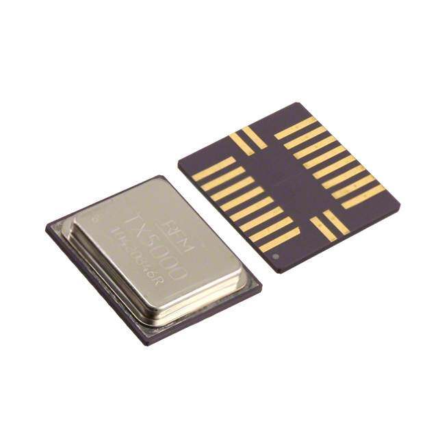
ICGOO电子元器件商城为您提供TX5000由Murata设计生产,在icgoo商城现货销售,并且可以通过原厂、代理商等渠道进行代购。 TX5000价格参考。MurataTX5000封装/规格:RF 发射器, RF Transmitter ASK, OOK 433.92MHz 0dBm 115.2kbps PCB, Surface Mount Antenna SM-20L。您可以下载TX5000参考资料、Datasheet数据手册功能说明书,资料中有TX5000 详细功能的应用电路图电压和使用方法及教程。
Murata Electronics North America的TX5000系列RF发射器主要应用于无线通信领域,具体应用场景包括:

1. 工业自动化:TX5000可用于工业设备之间的无线数据传输,例如传感器网络、远程监控和控制。它能够实现高效、稳定的信号发送,支持复杂的工业环境下的数据交换。

2. 消费电子:该型号适用于家用无线设备,如无线键盘、鼠标、游戏控制器等。通过其低功耗和高可靠性的特点,为用户提供流畅的使用体验。

3. 医疗设备:在医疗领域,TX5000可以用于可穿戴健康监测设备(如心率监测器、血糖仪)的数据传输,确保患者数据实时上传到云端或医生端进行分析。

4. 智能家居:作为智能家居系统的一部分,TX5000可用于智能照明、安防摄像头、门锁等设备的无线通信,提供快速响应和稳定连接。

5. 物联网(IoT):TX5000广泛应用于各种物联网设备中,支持M2M(机器对机器)通信,帮助构建智慧城市、智能农业、环境监测等解决方案。

6. 遥控与遥测:适用于无人机、玩具车等需要远程控制的场景,提供远距离、低延迟的信号传输能力。

TX5000以其紧凑的设计、低功耗特性和广泛的频率范围,成为众多无线应用的理想选择,满足不同行业对高性能RF发射器的需求。
| 参数 | 数值 |
| 产品目录 | |
| 描述 | ASH TX 115.2 KBPS 433.92 MHZ射频收发器 2G ASH Transmitter 433.92MHz 115.2 kbps |
| 产品分类 | |
| 品牌 | Murata Electronics |
| 产品手册 | |
| 产品图片 |
|
| rohs | 符合RoHS无铅 / 符合限制有害物质指令(RoHS)规范要求 |
| 产品系列 | RF集成电路,射频收发器,Murata Electronics TX5000TX |
| 数据手册 | |
| 产品型号 | TX5000 |
| 产品目录页面 | |
| 产品种类 | 射频收发器 |
| 其它名称 | 583-1096-1 |
| 功率-输出 | 0dBm |
| 包装 | 剪切带 (CT) |
| 发送机数量 | 1 |
| 商标 | Murata Electronics |
| 天线连接器 | PCB,表面贴装 |
| 存储容量 | - |
| 安装风格 | SMD/SMT |
| 封装 | Reel |
| 封装/外壳 | SM-20L |
| 封装/箱体 | SM-20L |
| 工作温度 | -40°C ~ 85°C |
| 工作电源电压 | 3.3 V |
| 工厂包装数量 | 250 |
| 应用 | 通用数据传输 |
| 接收机数量 | 1 |
| 数据接口 | PCB,表面贴装 |
| 数据速率(最大值) | 115.2kbps |
| 最大工作温度 | + 85 C |
| 最大数据速率 | 115.2 kb/s |
| 最小工作温度 | - 40 C |
| 标准包装 | 1 |
| 特性 | - |
| 电压-电源 | 2.2 V ~ 3.7 V |
| 电流-传输 | 7.5mA |
| 电源电压-最大 | 3.7 V |
| 电源电压-最小 | 2.2 V |
| 调制或协议 | ASK,OOK |
| 调制格式 | OOK/ASK |
| 频率 | 433.92MHz |
| 频率范围 | 433.92 MHz |


- 商务部:美国ITC正式对集成电路等产品启动337调查
- 曝三星4nm工艺存在良率问题 高通将骁龙8 Gen1或转产台积电
- 太阳诱电将投资9.5亿元在常州建新厂生产MLCC 预计2023年完工
- 英特尔发布欧洲新工厂建设计划 深化IDM 2.0 战略
- 台积电先进制程称霸业界 有大客户加持明年业绩稳了
- 达到5530亿美元!SIA预计今年全球半导体销售额将创下新高
- 英特尔拟将自动驾驶子公司Mobileye上市 估值或超500亿美元
- 三星加码芯片和SET,合并消费电子和移动部门,撤换高东真等 CEO
- 三星电子宣布重大人事变动 还合并消费电子和移动部门
- 海关总署:前11个月进口集成电路产品价值2.52万亿元 增长14.8%


PDF Datasheet 数据手册内容提取
RFM products are now Murata products. TX5000 • Designed for Short-Range Wireless Data Communications • Supports RF Data Transmission Rates Up to 115.2 kbps • 3 V, Low Current Operation plus Sleep Mode 433.92 MHz • Stable, Easy to Use, Low External Parts Count Hybrid Transmitter • Complies with Directive 2002/95/EC (RoHS) The TX5000 hybrid transmitter is ideal for short-range wireless data applications where robust operation, small size, low power consumption and low cost are required. All critical RF functions are contained in the hybrid, simplifying and speeding design- in. The TX5000 includes provisions for both on-off keyed (OOK) and amplitude-shift keyed (ASK) modulation. The TX5000 employs SAW filtering to suppress output harmonics, facilitating compliance with ETSI I-ETS 300 220 and similar regulations. Absolute Maximum Ratings Rating Value Units Power Supply and All Input/Output Pins -0.3 to +4.0 V SM-20L Case Non-Operating Case Temperature -50 to +100 °C Soldering Temperature (10 seconds / 5 cycles max.) 260 °C Electrical Characteristics Characteristic Sym Notes Minimum Typical Maximum Units Operating Frequency f 433.72 434.12 MHz o Modulation Types OOK & ASK OOK Data Rate 10 kbps ASK Data Rate 115.2 kbps Transmitter Performance Peak RF Output Power, 250 µA TXMOD Current P 0 dBm O Peak Current, 250 µA TXMOD Current I 7.5 mA TP OOK Turn On/Turn Off Times t /t 20/15 µs ON OFF ASK Output Rise/Fall Times t /t 1.1/1.1 µs TR TF 2nd - 4th Harmonic Outputs -50 dBm 5th - 10th Harmonic Outputs -55 dBm Non-harmonic Spurious Outputs -50 dBm Sleep Mode Current I 0.7 µA S Sleep to Transmit Switch Time t 21 µs TOR Transmit to Sleep Switch Time t 15 µs RTO Control Input Logic Low Level 200 mV Control Input Logic High Level 1 Vcc - 300 mV Power Supply Voltage Range V 2.2 3.7 Vdc CC Operating Ambient Temperature T -40 85 °C A ©2010-2015 by Murata Electronics N.A., Inc. www.murata.com TX5000 (R) 4/24/15 Page 1 of 6
Transmitter OOK Configuration Transmitter ASK Configuration + 3 + 3 CRFB2 VDC CDCB CRFB2 VDC CDCB + + T/S T/S 19 18 17 16 15 14 13 12 19 18 17 16 15 14 13 12 LAT GN3D CRNL0T CRNL1T VC2C WIDPTH RAPTE TH1LD TH2LD LAT GND CNT CNT VCC P P THLD THLD 20 RFIO TOP VIEW RREF 11 20 RF3IO RL0 RL1 2 WIDTH RATE 1 RR2EF 11 TOP VIEW LESD 1 GVCN1CD1 ACGAPC DPEKT OBUBT CIMNP DRAXTA MTOXD GANLPDDFJ2 10 LESD 1 GVCNCD1 AGC PK BB CMP RX TX GNLPDF2 10 2 3 4 5 6 7 8 9 1 CAP DET OUT IN DATA MOD ADJ LRFB RTXM 2LRFB 3 4 5 6 7 8 9 + 3 CRFB1 Modulation Input C RTXM VDC + 3 RFB1 Modulation Input VDC Transmitter Set-Up, 3.0 Vdc, -40 to +85 °C Item Symbol OOK ASK ASK Units Notes Nominal NRZ Data Rate DR 2.4 19.2 115.2 kbps see page 1 NOM Minimum Signal Pulse SP 416.67 52.08 8.68 µs single bit MIN Maximum Signal Pulse SP 1666.68 208.32 34.72 µs 4 bits of same value MAX TXMOD Resistor R 8.2 8.2 8.2 K ±5%, for 0 dBm output TXM DC Bypass Capacitor C 4.7 4.7 4.7 µF tantalum DCB RF Bypass Capacitor 1 C 27 27 27 pF ±5% NPO RFB1 RF Bypass Capacitor 2 C 100 100 100 pF ±5% NPO RFB2 RF Bypass Bead L Fair-Rite Fair-Rite Fair-Rite vendor 2506033017YO or equivalent RFB Series Tuning Inductor L 56 56 56 nH 50 ohm antenna AT Shunt Tuning/ESD Inductor L 220 220 220 nH 50 ohm antenna ESD CAUTION: Electrostatic Sensitive Device. Observe precautions for handling. NOTES: 1. Do not allow the voltage applied to a control input pin to exceed Vcc + 200 mV. 2. The companion receiver to the TX5000 is the RX5000. Please see Murata’s web site at www.rfm.com for details. ©2010-2015 by Murata Electronics N.A., Inc. www.murata.com TX5000 (R) 4/24/15 Page 2 of 6
Transmitter Theory of Operation Transmitter Chain The transmitter chain consists of a SAW coupled-resonator oscillator followed by a modulated buffer amplifier. The SAW Introduction coupled resonator output filter suppresses transmitter harmonics Murata’s TX-series hybrid transmitters are specifically designed for to the antenna. short-range wireless data communication applications. These transmitters provide robust operation, very small size, low power Transmitter operation supports two modulation formats, on-off consumption and low implementation cost. All critical RF functions keyed (OOK) modulation, and amplitude-shift keyed (ASK) are contained in the hybrid, simplifying and speeding design-in. modulation. When OOK modulation is chosen, the transmitter The transmitters can be readily configured to support a wide output turns completely off between “1” data pulses. When ASK range of data rates and protocol requirements. TX-series modulation is chosen, a “1” pulse is represented by a higher transmitters feature excellent suppression of output harmonics and transmitted power level, and a “0” is represented by a lower virtually no other RF emissions, making them easy to certify to transmitted power level. OOK modulation provides compatibility short- range (unlicensed) radio regulations. with first-generation ASH technology, and provides for power conservation. ASK modulation must be used for high data rates Transmitter Block Diagram (data pulses less than 200 µs). ASK modulation also reduces the Figure 1 is the general block diagram of the transmitter. Please effects of some types of interference and allows the transmitted refer to Figure 1 for the following discussions. pulses to be shaped to control modulation bandwidth. Antenna Port The modulation format is chosen by the state of the CNTRL0 and The only external RF components needed for the transmitter are the CNTRL1 mode control pins, as discussed below. In the OOK the antenna and its matching components. Antennas presenting mode, the oscillator amplifier TXA1 and buffer amplifier TXA2 are an impedance in the range of 35 to 72 ohms resistive can be turned off when the voltage to the TXMOD input falls below 220 satisfactorily matched to the RFIO pin with a series matching coil mV. In the OOK mode, the data rate is limited by the 20/15 µs turn- and a shunt matching/ESD protection coil. Other antenna on and turn-off time of the oscillator. In the ASK mode TXA1 is impedances can be matched using two or three components. For biased ON continuously, and the output of TXA2 is modulated by some impedances, two inductors and a capacitor will be required. the TXMOD input current. Minimum output power occurs in the A DC path from RFIO to ground is required for ESD protection. ASK mode when the modulation driver sinks about 10 µA of Transmitter Block Diagram Antenna SAW Coupled Resonator Ant SAW Tune TXA1 TXA2 CR Filter Tune/ESD Modulation & Bias Control R TXM TX CN CN IN TRL1 TRL0 Figure 1 ©2010-2015 by Murata Electronics N.A., Inc. www.murata.com TX5000 (R) 4/24/15 Page 3 of 6
The transmitter RF output power is proportional to the input current Turn-On Timing to the TXMOD pin. A series resistor is used to adjust the peak The maximum time required for either the OOK or ASK transmitter transmitter output power. 0 dBm of output power requires about mode to become operational is 5 ms after the supply voltage 250 µA of input current. reaches 2.2 Vdc. The total turn-on time to stable transmitter Transmitter Mode Control operation for a 10 ms power supply rise time is 15 ms. The three transmitter operating modes – transmit ASK, transmit Sleep and Wake-Up Timing OOK, and power-down (sleep), are controlled by the Modulation & The maximum transition time from either transmit mode to the Bias Control function, and are selected with the CNTRL1 and sleep mode (t and t ) is 15 µs after CNTRL1 and CNTRL0 TOS TAS CNTRL0 control pins. Setting CNTRL1 high and CNTRL0 low are both low (1 µs fall time). place the unit in the ASK transmit mode. Setting CNTRL1 low and The maximum time required to switch from the sleep mode to CNTRL0 high place the unit in the OOK transmit mode. Setting either transmit mode (t and t ) is 21 µs. Most of this time is CNTRL1 and CNTRL0 both low place the unit in the power-down STO STA due to the start-up of the transmitter oscillator. mode. (Note that the resistor driving TXMOD must also be low in the power-down mode to minimize power-down current.) CNTRL1 and CNTRL0 are CMOS compatible inputs. These inputs must be held at a logic level; they cannot be left unconnected. Transmitter Pin Out SM-20L Package Drawing GND1 RFIO B C D 1 20 E VCC1 2 19 GND3 NC 3 18 CNTRL0 NC 4 17 CNTRL1 F NC 5 16 VCC2 A NC 6 15 NC NC 7 14 NC TXMOD 8 13 NC H NC 9 12 NC 10 11 G GND2 NC mm Inches SM-20L PCB Pad Layout Dimension Min Nom Max Min Nom Max 52 7525 75 17 1912 23 A 10.795 10.922 11.04 .425 .430 .435 . .. . 9 .4600 B 9.525 9.652 9.779 .375 .380 .385 C 1.778 1.905 2.032 .070 .075 .080 .3825 .3575 D 3.048 3.175 3.302 .120 .125 .130 .3175 E 0.381 0.508 0.635 .015 .020 .025 .2775 F 0.889 1.016 1.143 .035 .040 .045 .2375 G 3.175 3.302 3.429 .125 .130 .135 .1975 H 1.778 1.905 2.032 .070 .075 0.80 .1575 .1175 .1025 .0775 0000. 0.000401. 270. 410. Dimensions in inches ©2010-2015 by Murata Electronics N.A., Inc. www.murata.com TX5000 (R) 4/24/15 Page 4 of 6
Pin Name Description 1 GND1 GND1 is the RF ground pin. GND2 and GND3 should be connected to GND1 by short, low-inductance traces. VCC1 is the positive supply voltage pin for the transmitter output amplifier and the transmitter base-band circuitry. VCC1 is 2 VCC1 usually connected to the positive supply through a ferrite RF decoupling bead which is bypassed by an RF capacitor on the supply side. See the description of VCC2 (Pin 16) for additional information. 3 NC No connection. Printed circuit board pad may be grounded or floating. 4 NC No connection. Printed circuit board pad may be grounded or floating. 5 NC No connection. Printed circuit board pad may be grounded or floating. 6 NC No connection. Printed circuit board pad may be grounded or floating. 7 NC No connection. Printed circuit board pad may be grounded or floating. The transmitter RF output voltage is proportional to the input current to this pin. A series resistor is used to adjust the peak transmitter output voltage. 0 dBm of output power requires 250 µA of input current. In the ASK mode, minimum output power occurs when the modulation driver sinks about 10 µA of current from this pin. In the OOK mode, input signals less than 220 mV completely turn the transmitter oscillator off. Internally, this pin appears to be a diode in series with a small resistor. Peak transmitter output power P for a 3 Vdc supply voltage is approximately: O 8 TXMOD P = 16*(I )2, where P is in mW, and the peak modulation current I is in mA O TXM O TXM A ±5% resistor value is recommended. In the OOK mode, this pin is usually driven with a logic-level data input (unshaped data pulses). OOK modulation is practical for data pulses of 200 µs or longer. In the ASK mode, this pin accepts analog mod- ulation (shaped or unshaped data pulses). ASK modulation is practical for data pulses 8.7 µs or longer. This pin must be low in the power-down (sleep) mode. Please refer to the ASH Transceiver Designer’s Guide for additional information on modula- tion techniques. 9 NC No connection. Printed circuit board pad may be grounded or floating. 10 GND2 GND2 is an IC ground pin. It should be connected to GND1 by a short, low inductance trace. 11 NC No connection. Printed circuit board pad may be grounded or floating. 12 NC No connection. Printed circuit board pad may be grounded or floating. 13 NC No connection. Printed circuit board pad may be grounded or floating. 14 NC No connection. Printed circuit board pad may be grounded or floating. 15 NC No connection. Printed circuit board pad may be grounded or floating. VCC2 is the positive supply voltage pin for the transmitter oscillator. Pin 16 must be bypassed with an RF capacitor, and must 16 VCC2 also be bypassed with a 1 to 10 µF tantalum or electrolytic capacitor. Power supply voltage ripple should be limited to 10 mV peak-to-peak. See the ASH Transceiver Designer’s Guide for additional information. CNTRL1 and CNTRL0 select the transmit modes. CNTRL1 high and CNTRL0 low place the unit in the ASK transmit mode. CNTRL1 low and CNTRL0 high place the unit in the OOK transmit mode. CNTRL1 and CNTRL0 both low place the unit in the power-down (sleep) mode. CNTRL1 is a high-impedance input (CMOS compatible). An input voltage of 0 to 300 mV is 17 CNTRL1 interpreted as a logic low. An input voltage of Vcc - 300 mV or greater is interpreted as a logic high. An input voltage greater than Vcc + 200 mV should not be applied to this pin. A logic high requires a maximum source current of 40 µA. A logic low requires a maximum sink current of 25 µA (1 µA in sleep mode). This pin must be held at a logic level; it cannot be left uncon- nected. CNTRL0 is used with CNTRL1 to control the operating modes of the transmitter. See the description of CNTRL1 for more 18 CNTRL0 information. 19 GND3 GND3 is an IC ground pin. It should be connected to GND1 by a short, low inductance trace. RFIO is the transmitter RF output pin. This pin is connected directly to the SAW filter transducer. Antennas presenting an impedance in the range of 35 to 72 ohms resistive can be satisfactorily matched to this pin with a series matching coil and a 20 RFIO shunt matching/ESD protection coil. Other antenna impedances can be matched using two or three components. For some impedances, two inductors and a capacitor will be required. A DC path from RFIO to ground is required for ESD protection. ©2010-2015 by Murata Electronics N.A., Inc. www.murata.com TX5000 (R) 4/24/15 Page 5 of 6
RF Output Power vs I TXM 1.60 1.40 3 V 1.20 W m 1.00 n er i w 0.80 o P t u p ut 0.60 O 0.40 0.20 25 50 75 100 125 150 175 200 225 250 275 I in µA TXM V vs I TXM TXM 1.20 1.15 1.10 1.05 V n iM1.00 VTX 0.95 0.90 0.85 25 50 75 100 125 150 175 200 225 250 275 I in µA TXM Note: Specifications subject to change without notice. ©2010-2015 by Murata Electronics N.A., Inc. www.murata.com TX5000 (R) 4/24/15 Page 6 of 6