ICGOO在线商城 > 开发板,套件,编程器 > 评估板 - 嵌入式 - MCU,DSP > TWR-S12G64-KIT

 Datasheet下载
- 型号: TWR-S12G64-KIT
- 制造商: Freescale Semiconductor
- 库位|库存: xxxx|xxxx
- 要求:
| 数量阶梯 | 香港交货 | 国内含税 |
| +xxxx | $xxxx | ¥xxxx |
查看当月历史价格
查看今年历史价格
TWR-S12G64-KIT产品简介:
ICGOO电子元器件商城为您提供TWR-S12G64-KIT由Freescale Semiconductor设计生产,在icgoo商城现货销售,并且可以通过原厂、代理商等渠道进行代购。 TWR-S12G64-KIT价格参考。Freescale SemiconductorTWR-S12G64-KIT封装/规格:评估板 - 嵌入式 - MCU,DSP, MC9S12G Tower System HCS12 HCS12 MCU 16-Bit Embedded Evaluation Board。您可以下载TWR-S12G64-KIT参考资料、Datasheet数据手册功能说明书,资料中有TWR-S12G64-KIT 详细功能的应用电路图电压和使用方法及教程。
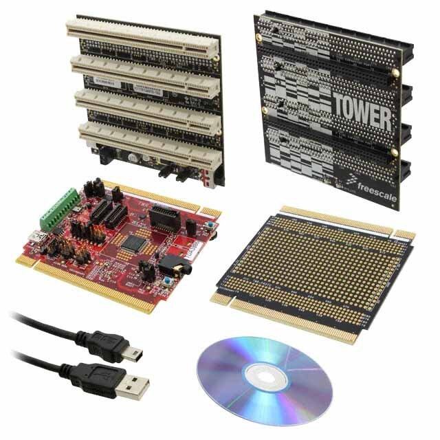
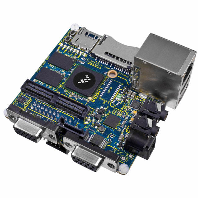
NXP USA Inc. 的 TWR-S12G64-KIT 是一款基于S12G微控制器的塔式(Tower)评估板,属于嵌入式MCU评估板系列。该开发套件主要用于汽车电子和工业控制领域的原型设计与开发。

典型应用场景包括:汽车车身控制系统,如车门模块、车灯控制、雨刷控制和HVAC(暖通空调)系统;车载传感器接口开发;以及需要符合AEC-Q100标准的汽车级MCU验证。此外,该套件适用于学习和开发基于16位S12架构的嵌入式应用,支持CAN、LIN等车载通信协议,便于进行网络节点开发与测试。

在工业控制方面,可用于电机控制、智能执行器和低功耗实时控制系统的开发。TWR-S12G64-KIT 搭配 CodeWarrior 或 S32 Design Studio 等开发环境,便于快速进行代码调试和硬件验证,适合工程师、研究人员及高校师生用于教学实验和项目原型搭建。

其模块化设计可与其他Tower系列扩展板(如传感器、通信模块)配合使用,提升开发灵活性。总体而言,该评估板适用于需要高可靠性、实时控制能力及汽车级认证的嵌入式应用开发场景。
| 参数 | 数值 |
| 产品目录 | 编程器,开发系统 |
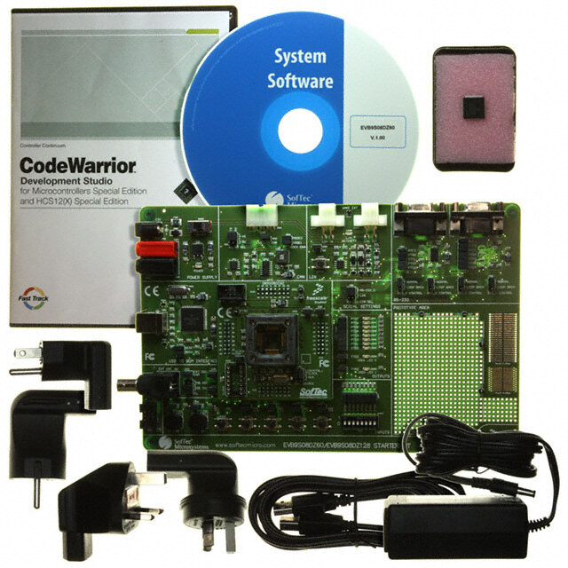
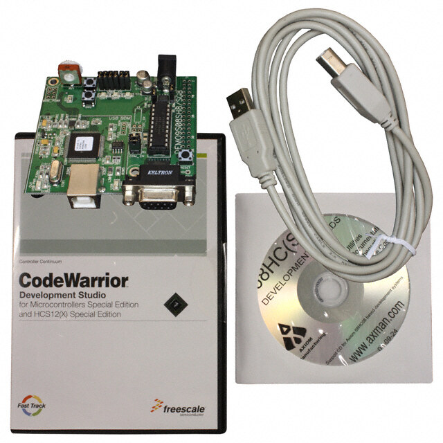
| 描述 | KIT HDWR TOWER S12G64 |
| 产品分类 | 评估板 - 嵌入式 - MCU, DSP |
| 品牌 | Freescale Semiconductor |
| 数据手册 | |
| 产品图片 |
|
| 产品型号 | TWR-S12G64-KIT |
| rohs | 无铅 / 符合限制有害物质指令(RoHS)规范要求 |
| 产品系列 | HCS12 |
| 内容 | 板,电缆 |
| 安装类型 | 固定 |
| 平台 | Freescale Tower System |
| 操作系统 | - |
| 板类型 | 评估平台 |
| 标准包装 | 1 |
| 核心处理器 | HCS12 |
| 类型 | MCU 16-位 |
| 配套使用产品/相关产品 | MC9S12G |


- 商务部:美国ITC正式对集成电路等产品启动337调查
- 曝三星4nm工艺存在良率问题 高通将骁龙8 Gen1或转产台积电
- 太阳诱电将投资9.5亿元在常州建新厂生产MLCC 预计2023年完工
- 英特尔发布欧洲新工厂建设计划 深化IDM 2.0 战略
- 台积电先进制程称霸业界 有大客户加持明年业绩稳了
- 达到5530亿美元!SIA预计今年全球半导体销售额将创下新高
- 英特尔拟将自动驾驶子公司Mobileye上市 估值或超500亿美元
- 三星加码芯片和SET,合并消费电子和移动部门,撤换高东真等 CEO
- 三星电子宣布重大人事变动 还合并消费电子和移动部门
- 海关总署:前11个月进口集成电路产品价值2.52万亿元 增长14.8%
PDF Datasheet 数据手册内容提取
MC9S12G Family Reference Manual and Data Sheet S12 Microcontrollers MC9S12GRMV1 Rev.1.27 October 23, 2017 nxp.com
To provide the most up-to-date information, the revision of our documents on the World Wide Web will be the most current. Your printed copy may be an earlier revision. To verify you have the latest information available, refer to: nxp.com/ A full list of family members and options is included in the appendices. MC9S12G Family Reference Manual Rev.1.27 NXP Semiconductors 2
The following revision history table summarizes changes contained in this document. Revision History Revision Date Description Level • Added Chapter12, “Analog-to-Digital Converter (ADC12B8CV2)” • Added Chapter14, “Analog-to-Digital Converter (ADC12B12CV2)” • Updated Chapter11, “Analog-to-Digital Converter (ADC10B8CV2)” (Reason: Spec update) • Updated Chapter13, “Analog-to-Digital Converter (ADC10B12CV2)” Nov, 2012 1.18 (Reason: Spec update) • Updated Chapter15, “Analog-to-Digital Converter (ADC10B16CV2)” (Reason: Spec update) • Updated Chapter16, “Analog-to-Digital Converter (ADC12B16CV2)” (Reason: Spec update) Nov, 2012 1.19 • Corrected order of chapters • Updated AppendixA, “Electrical Characteristics” (Reason: Added AEC Grade 0 spec) Jan, 2013 1.20 • Updated AppendixC, “Ordering and Shipping Information” (Reason: Added temperature option W) • Separated description of 8-channel timer Jan, 2013 1.21 • Updated AppendixA, “Electrical Characteristics” (Reason: Updated electricals) • Updated Chapter1, “Device Overview MC9S12G-Family” (Reason: added KGD option for the S12GA192 and the S12GA240) • Updated AppendixA, “Electrical Characteristics” (Reason: Updated electricals) Jan, 2013 1.22 • Up[dated AppendixC, “Ordering and Shipping Information” (Reason: Added KGD information) • Added AppendixD, “Package and Die Information” (Reason: Added KGD information) • Updated AppendixC, “Ordering and Shipping Information” Feb, 2013 1.23 (Reason: Removed KGD information) • Updated Chapter1, “Device Overview MC9S12G-Family” (Reason: Spec update) • Fixed wordingFixed typos and formatting, improved wording Jul, 2014 1.24 • Updated AppendixA, “Electrical Characteristics” (Reason: Updated electricals) • Updated Chapter17, “Digital Analog Converter (DAC_8B5V)” (Reason: Spec update) Aug, 2014 1.25 • Fixed issues with hidden text throughout the document • Updated Chapter1, “Device Overview MC9S12G-Family Jun, 2017 1.26 (added mask set information to Table1-5) • Updated AppendixA, “Electrical Characteristics Oct, 2017 1.27 (updated TableA-44 and TableA-45) MC9S12G Family Reference Manual Rev.1.27 NXP Semiconductors 3
This document contains information for all constituent modules, with the exception of the CPU. For CPU information please refer to CPU12-1 in the CPU12 & CPU12X Reference Manual MC9S12G Family Reference Manual Rev.1.27 4 NXP Semiconductors
Chapter 1 Device Overview MC9S12G-Family . . . . . . . . . . . . . . . . . . . . . . . . . . . . . .29 Chapter 2 Port Integration Module (S12GPIMV1) . . . . . . . . . . . . . . . . . . . . . . . . . . .149 Chapter 3 5V Analog Comparator (ACMPV1) . . . . . . . . . . . . . . . . . . . . . . . . . . . . . .249 Chapter 4 Reference Voltage Attenuator (RVAV1). . . . . . . . . . . . . . . . . . . . . . . . . .255 Chapter 5 S12G Memory Map Controller (S12GMMCV1). . . . . . . . . . . . . . . . . . . . .259 Chapter 6 Interrupt Module (S12SINTV1). . . . . . . . . . . . . . . . . . . . . . . . . . . . . . . . . .273 Chapter 7 Background Debug Module (S12SBDMV1) . . . . . . . . . . . . . . . . . . . . . . .281 Chapter 8 S12S Debug Module (S12SDBGV2) . . . . . . . . . . . . . . . . . . . . . . . . . . . . .305 Chapter 9 Security (S12XS9SECV2). . . . . . . . . . . . . . . . . . . . . . . . . . . . . . . . . . . . . .347 Chapter 10 S12 Clock, Reset and Power Management Unit (S12CPMU) . . . . . . . . .353 Chapter 11 Analog-to-Digital Converter (ADC10B8CV2) . . . . . . . . . . . . . . . . . . . . . .405 Chapter 12 Analog-to-Digital Converter (ADC12B8CV2) . . . . . . . . . . . . . . . . . . . . . .429 Chapter 13 Analog-to-Digital Converter (ADC10B12CV2) . . . . . . . . . . . . . . . . . . . . .455 Chapter 14 Analog-to-Digital Converter (ADC12B12CV2) . . . . . . . . . . . . . . . . . . . . .481 Chapter 15 Analog-to-Digital Converter (ADC10B16CV2) . . . . . . . . . . . . . . . . . . . . .507 Chapter 16 Analog-to-Digital Converter (ADC12B16CV2) . . . . . . . . . . . . . . . . . . . . .533 Chapter 17 Digital Analog Converter (DAC_8B5V). . . . . . . . . . . . . . . . . . . . . . . . . . .559 Chapter 18 Scalable Controller Area Network (S12MSCANV3). . . . . . . . . . . . . . . . .569 Chapter 19 Pulse-Width Modulator (S12PWM8B8CV2) . . . . . . . . . . . . . . . . . . . . . . .623 Chapter 20 Serial Communication Interface (S12SCIV5). . . . . . . . . . . . . . . . . . . . . .653 Chapter 21 Serial Peripheral Interface (S12SPIV5). . . . . . . . . . . . . . . . . . . . . . . . . . .691 Chapter 22 Timer Module (TIM16B6CV3). . . . . . . . . . . . . . . . . . . . . . . . . . . . . . . . . . .719 Chapter 23 Timer Module (TIM16B8CV3). . . . . . . . . . . . . . . . . . . . . . . . . . . . . . . . . . .737 Chapter 24 16 KByte Flash Module (S12FTMRG16K1V1) . . . . . . . . . . . . . . . . . . . . .765 Chapter 25 32 KByte Flash Module (S12FTMRG32K1V1) . . . . . . . . . . . . . . . . . . . . .813 Chapter 26 48 KByte Flash Module (S12FTMRG48K1V1) . . . . . . . . . . . . . . . . . . . . .865 Chapter 27 64 KByte Flash Module (S12FTMRG64K1V1) . . . . . . . . . . . . . . . . . . . . .917 Chapter 28 96 KByte Flash Module (S12FTMRG96K1V1) . . . . . . . . . . . . . . . . . . . . .969 Chapter 29 128 KByte Flash Module (S12FTMRG128K1V1) . . . . . . . . . . . . . . . . . .1021 Chapter 30 192 KByte Flash Module (S12FTMRG192K2V1) . . . . . . . . . . . . . . . . . .1073 Chapter 31 240 KByte Flash Module (S12FTMRG240K2V1) . . . . . . . . . . . . . . . . . .1125 MC9S12G Family Reference Manual Rev.1.27 NXP Semiconductors 5
Appendix A Electrical Characteristics . . . . . . . . . . . . . . . . . . . . . . . . . . . . . . . . . . . .1177 Appendix B Detailed Register Address Map . . . . . . . . . . . . . . . . . . . . . . . . . . . . . . .1233 Appendix C Ordering and Shipping Information . . . . . . . . . . . . . . . . . . . . . . . . . . . .1253 Appendix D Package and Die Information . . . . . . . . . . . . . . . . . . . . . . . . . . . . . . . . .1255 MC9S12G Family Reference Manual Rev.1.27 6 NXP Semiconductors
Chapter 1 Device Overview MC9S12G-Family 1.1 Introduction . . . . . . . . . . . . . . . . . . . . . . . . . . . . . . . . . . . . . . . . . . . . . . . . . . . . . . . . . . . . . . . . . . 29 1.2 Features . . . . . . . . . . . . . . . . . . . . . . . . . . . . . . . . . . . . . . . . . . . . . . . . . . . . . . . . . . . . . . . . . . . . . 30 1.2.1 MC9S12G-Family Comparison . . . . . . . . . . . . . . . . . . . . . . . . . . . . . . . . . . . . . . . . . . . . 30 1.2.2 Chip-Level Features . . . . . . . . . . . . . . . . . . . . . . . . . . . . . . . . . . . . . . . . . . . . . . . . . . . . . 32 1.3 Module Features . . . . . . . . . . . . . . . . . . . . . . . . . . . . . . . . . . . . . . . . . . . . . . . . . . . . . . . . . . . . . . . 32 1.3.1 S12 16-Bit Central Processor Unit (CPU) . . . . . . . . . . . . . . . . . . . . . . . . . . . . . . . . . . . . 33 1.3.2 On-Chip Flash with ECC . . . . . . . . . . . . . . . . . . . . . . . . . . . . . . . . . . . . . . . . . . . . . . . . . 33 1.3.3 On-Chip SRAM . . . . . . . . . . . . . . . . . . . . . . . . . . . . . . . . . . . . . . . . . . . . . . . . . . . . . . . . 33 1.3.4 Port Integration Module (PIM) . . . . . . . . . . . . . . . . . . . . . . . . . . . . . . . . . . . . . . . . . . . . 33 1.3.5 Main External Oscillator (XOSCLCP) . . . . . . . . . . . . . . . . . . . . . . . . . . . . . . . . . . . . . . 34 1.3.6 Internal RC Oscillator (IRC) . . . . . . . . . . . . . . . . . . . . . . . . . . . . . . . . . . . . . . . . . . . . . . 34 1.3.7 Internal Phase-Locked Loop (IPLL) . . . . . . . . . . . . . . . . . . . . . . . . . . . . . . . . . . . . . . . . 34 1.3.8 System Integrity Support . . . . . . . . . . . . . . . . . . . . . . . . . . . . . . . . . . . . . . . . . . . . . . . . . 35 1.3.9 Timer (TIM) . . . . . . . . . . . . . . . . . . . . . . . . . . . . . . . . . . . . . . . . . . . . . . . . . . . . . . . . . . . 35 1.3.10 Pulse Width Modulation Module (PWM) . . . . . . . . . . . . . . . . . . . . . . . . . . . . . . . . . . . . 35 1.3.11 Controller Area Network Module (MSCAN) . . . . . . . . . . . . . . . . . . . . . . . . . . . . . . . . . 35 1.3.12 Serial Communication Interface Module (SCI) . . . . . . . . . . . . . . . . . . . . . . . . . . . . . . . . 36 1.3.13 Serial Peripheral Interface Module (SPI) . . . . . . . . . . . . . . . . . . . . . . . . . . . . . . . . . . . . . 36 1.3.14 Analog-to-Digital Converter Module (ADC) . . . . . . . . . . . . . . . . . . . . . . . . . . . . . . . . . 36 1.3.15 Reference Voltage Attenuator (RVA) . . . . . . . . . . . . . . . . . . . . . . . . . . . . . . . . . . . . . . . . 37 1.3.16 Digital-to-Analog Converter Module (DAC) . . . . . . . . . . . . . . . . . . . . . . . . . . . . . . . . . 37 1.3.17 Analog Comparator (ACMP) . . . . . . . . . . . . . . . . . . . . . . . . . . . . . . . . . . . . . . . . . . . . . . 37 1.3.18 On-Chip Voltage Regulator (VREG) . . . . . . . . . . . . . . . . . . . . . . . . . . . . . . . . . . . . . . . . 37 1.3.19 Background Debug (BDM) . . . . . . . . . . . . . . . . . . . . . . . . . . . . . . . . . . . . . . . . . . . . . . . 37 1.3.20 Debugger (DBG) . . . . . . . . . . . . . . . . . . . . . . . . . . . . . . . . . . . . . . . . . . . . . . . . . . . . . . . 37 1.4 Key Performance Parameters . . . . . . . . . . . . . . . . . . . . . . . . . . . . . . . . . . . . . . . . . . . . . . . . . . . . . 38 1.5 Block Diagram . . . . . . . . . . . . . . . . . . . . . . . . . . . . . . . . . . . . . . . . . . . . . . . . . . . . . . . . . . . . . . . . 38 1.6 Family Memory Map . . . . . . . . . . . . . . . . . . . . . . . . . . . . . . . . . . . . . . . . . . . . . . . . . . . . . . . . . . . 39 1.6.1 Part ID Assignments . . . . . . . . . . . . . . . . . . . . . . . . . . . . . . . . . . . . . . . . . . . . . . . . . . . . 44 1.7 Signal Description and Device Pinouts . . . . . . . . . . . . . . . . . . . . . . . . . . . . . . . . . . . . . . . . . . . . . 45 1.7.1 Pin Assignment Overview . . . . . . . . . . . . . . . . . . . . . . . . . . . . . . . . . . . . . . . . . . . . . . . . 45 1.7.2 Detailed Signal Descriptions . . . . . . . . . . . . . . . . . . . . . . . . . . . . . . . . . . . . . . . . . . . . . . 46 1.7.3 Power Supply Pins . . . . . . . . . . . . . . . . . . . . . . . . . . . . . . . . . . . . . . . . . . . . . . . . . . . . . . 50 1.8 Device Pinouts . . . . . . . . . . . . . . . . . . . . . . . . . . . . . . . . . . . . . . . . . . . . . . . . . . . . . . . . . . . . . . . . 53 1.8.1 S12GN16 and S12GN32 . . . . . . . . . . . . . . . . . . . . . . . . . . . . . . . . . . . . . . . . . . . . . . . . . 53 1.8.2 S12GNA16 and S12GNA32 . . . . . . . . . . . . . . . . . . . . . . . . . . . . . . . . . . . . . . . . . . . . . . 60 1.8.3 S12GN48 . . . . . . . . . . . . . . . . . . . . . . . . . . . . . . . . . . . . . . . . . . . . . . . . . . . . . . . . . . . . . 62 1.8.4 S12G48 and S12G64 . . . . . . . . . . . . . . . . . . . . . . . . . . . . . . . . . . . . . . . . . . . . . . . . . . . . 72 1.8.5 S12GA48 and S12GA64 . . . . . . . . . . . . . . . . . . . . . . . . . . . . . . . . . . . . . . . . . . . . . . . . . 82 1.8.6 S12G96 and S12G128 . . . . . . . . . . . . . . . . . . . . . . . . . . . . . . . . . . . . . . . . . . . . . . . . . . . 89 1.8.7 S12GA96 and S12GA128 . . . . . . . . . . . . . . . . . . . . . . . . . . . . . . . . . . . . . . . . . . . . . . . 101 1.8.8 S12G192 and S12G240 . . . . . . . . . . . . . . . . . . . . . . . . . . . . . . . . . . . . . . . . . . . . . . . . . 113 1.8.9 S12GA192 and S12GA240 . . . . . . . . . . . . . . . . . . . . . . . . . . . . . . . . . . . . . . . . . . . . . . 125 MC9S12G Family Reference Manual Rev.1.27 NXP Semiconductors 9
1.9 System Clock Description . . . . . . . . . . . . . . . . . . . . . . . . . . . . . . . . . . . . . . . . . . . . . . . . . . . . . . 140 1.10 Modes of Operation . . . . . . . . . . . . . . . . . . . . . . . . . . . . . . . . . . . . . . . . . . . . . . . . . . . . . . . . . . . 140 1.10.1 Chip Configuration Summary . . . . . . . . . . . . . . . . . . . . . . . . . . . . . . . . . . . . . . . . . . . . 141 1.10.2 Low Power Operation . . . . . . . . . . . . . . . . . . . . . . . . . . . . . . . . . . . . . . . . . . . . . . . . . . 141 1.11 Security . . . . . . . . . . . . . . . . . . . . . . . . . . . . . . . . . . . . . . . . . . . . . . . . . . . . . . . . . . . . . . . . . . . . . 141 1.12 Resets and Interrupts . . . . . . . . . . . . . . . . . . . . . . . . . . . . . . . . . . . . . . . . . . . . . . . . . . . . . . . . . . 141 1.12.1 Resets . . . . . . . . . . . . . . . . . . . . . . . . . . . . . . . . . . . . . . . . . . . . . . . . . . . . . . . . . . . . . . . 141 1.12.2 Interrupt Vectors . . . . . . . . . . . . . . . . . . . . . . . . . . . . . . . . . . . . . . . . . . . . . . . . . . . . . . 142 1.12.3 Effects of Reset . . . . . . . . . . . . . . . . . . . . . . . . . . . . . . . . . . . . . . . . . . . . . . . . . . . . . . . 144 1.13 COP Configuration . . . . . . . . . . . . . . . . . . . . . . . . . . . . . . . . . . . . . . . . . . . . . . . . . . . . . . . . . . . . 144 1.14 Autonomous Clock (ACLK) Configuration . . . . . . . . . . . . . . . . . . . . . . . . . . . . . . . . . . . . . . . . . 145 1.15 ADC External Trigger Input Connection . . . . . . . . . . . . . . . . . . . . . . . . . . . . . . . . . . . . . . . . . . . 145 1.16 ADC Special Conversion Channels . . . . . . . . . . . . . . . . . . . . . . . . . . . . . . . . . . . . . . . . . . . . . . . 145 1.17 ADC Result Reference . . . . . . . . . . . . . . . . . . . . . . . . . . . . . . . . . . . . . . . . . . . . . . . . . . . . . . . . . 146 1.18 ADC VRH/VRL Signal Connection . . . . . . . . . . . . . . . . . . . . . . . . . . . . . . . . . . . . . . . . . . . . . . 146 1.19 BDM Clock Source Connectivity . . . . . . . . . . . . . . . . . . . . . . . . . . . . . . . . . . . . . . . . . . . . . . . . 147 Chapter 2 Port Integration Module (S12GPIMV1) 2.1 Introduction . . . . . . . . . . . . . . . . . . . . . . . . . . . . . . . . . . . . . . . . . . . . . . . . . . . . . . . . . . . . . . . . . 149 2.1.1 Glossary . . . . . . . . . . . . . . . . . . . . . . . . . . . . . . . . . . . . . . . . . . . . . . . . . . . . . . . . . . . . . 149 2.1.2 Overview . . . . . . . . . . . . . . . . . . . . . . . . . . . . . . . . . . . . . . . . . . . . . . . . . . . . . . . . . . . . 150 2.1.3 Features . . . . . . . . . . . . . . . . . . . . . . . . . . . . . . . . . . . . . . . . . . . . . . . . . . . . . . . . . . . . . 150 2.1.4 Block Diagram . . . . . . . . . . . . . . . . . . . . . . . . . . . . . . . . . . . . . . . . . . . . . . . . . . . . . . . . 151 2.2 PIM Routing - External Signal Description . . . . . . . . . . . . . . . . . . . . . . . . . . . . . . . . . . . . . . . . . 151 2.2.1 Package Code . . . . . . . . . . . . . . . . . . . . . . . . . . . . . . . . . . . . . . . . . . . . . . . . . . . . . . . . . 152 2.2.2 Prioritization . . . . . . . . . . . . . . . . . . . . . . . . . . . . . . . . . . . . . . . . . . . . . . . . . . . . . . . . . 152 2.2.3 Signals and Priorities . . . . . . . . . . . . . . . . . . . . . . . . . . . . . . . . . . . . . . . . . . . . . . . . . . . 152 2.3 PIM Routing - Functional description . . . . . . . . . . . . . . . . . . . . . . . . . . . . . . . . . . . . . . . . . . . . . 154 2.3.1 Pin BKGD . . . . . . . . . . . . . . . . . . . . . . . . . . . . . . . . . . . . . . . . . . . . . . . . . . . . . . . . . . . 163 2.3.2 Pins PA7-0 . . . . . . . . . . . . . . . . . . . . . . . . . . . . . . . . . . . . . . . . . . . . . . . . . . . . . . . . . . . 163 2.3.3 Pins PB7-0 . . . . . . . . . . . . . . . . . . . . . . . . . . . . . . . . . . . . . . . . . . . . . . . . . . . . . . . . . . . 163 2.3.4 Pins PC7-0 . . . . . . . . . . . . . . . . . . . . . . . . . . . . . . . . . . . . . . . . . . . . . . . . . . . . . . . . . . . 163 2.3.5 Pins PD7-0 . . . . . . . . . . . . . . . . . . . . . . . . . . . . . . . . . . . . . . . . . . . . . . . . . . . . . . . . . . . 165 2.3.6 Pins PE1-0 . . . . . . . . . . . . . . . . . . . . . . . . . . . . . . . . . . . . . . . . . . . . . . . . . . . . . . . . . . . 165 2.3.7 Pins PT7-0 . . . . . . . . . . . . . . . . . . . . . . . . . . . . . . . . . . . . . . . . . . . . . . . . . . . . . . . . . . . 165 2.3.8 Pins PS7-0 . . . . . . . . . . . . . . . . . . . . . . . . . . . . . . . . . . . . . . . . . . . . . . . . . . . . . . . . . . . 167 2.3.9 Pins PM3-0 . . . . . . . . . . . . . . . . . . . . . . . . . . . . . . . . . . . . . . . . . . . . . . . . . . . . . . . . . . 169 2.3.10 Pins PP7-0 . . . . . . . . . . . . . . . . . . . . . . . . . . . . . . . . . . . . . . . . . . . . . . . . . . . . . . . . . . . 169 2.3.11 Pins PJ7-0 . . . . . . . . . . . . . . . . . . . . . . . . . . . . . . . . . . . . . . . . . . . . . . . . . . . . . . . . . . . 171 2.3.12 Pins AD15-0 . . . . . . . . . . . . . . . . . . . . . . . . . . . . . . . . . . . . . . . . . . . . . . . . . . . . . . . . . 172 2.4 PIM Ports - Memory Map and Register Definition . . . . . . . . . . . . . . . . . . . . . . . . . . . . . . . . . . . 178 2.4.1 Memory Map . . . . . . . . . . . . . . . . . . . . . . . . . . . . . . . . . . . . . . . . . . . . . . . . . . . . . . . . . 178 2.4.2 Register Map . . . . . . . . . . . . . . . . . . . . . . . . . . . . . . . . . . . . . . . . . . . . . . . . . . . . . . . . . 181 2.4.3 Register Descriptions . . . . . . . . . . . . . . . . . . . . . . . . . . . . . . . . . . . . . . . . . . . . . . . . . . . 196 MC9S12G Family Reference Manual Rev.1.27 10 NXP Semiconductors
2.5 PIM Ports - Functional Description . . . . . . . . . . . . . . . . . . . . . . . . . . . . . . . . . . . . . . . . . . . . . . . 241 2.5.1 General . . . . . . . . . . . . . . . . . . . . . . . . . . . . . . . . . . . . . . . . . . . . . . . . . . . . . . . . . . . . . . 241 2.5.2 Registers . . . . . . . . . . . . . . . . . . . . . . . . . . . . . . . . . . . . . . . . . . . . . . . . . . . . . . . . . . . . . 241 2.5.3 Pin Configuration Summary . . . . . . . . . . . . . . . . . . . . . . . . . . . . . . . . . . . . . . . . . . . . . 243 2.5.4 Interrupts . . . . . . . . . . . . . . . . . . . . . . . . . . . . . . . . . . . . . . . . . . . . . . . . . . . . . . . . . . . . 244 2.6 Initialization/Application Information . . . . . . . . . . . . . . . . . . . . . . . . . . . . . . . . . . . . . . . . . . . . . 246 2.6.1 Initialization . . . . . . . . . . . . . . . . . . . . . . . . . . . . . . . . . . . . . . . . . . . . . . . . . . . . . . . . . . 246 2.6.2 Port Data and Data Direction Register writes . . . . . . . . . . . . . . . . . . . . . . . . . . . . . . . . 246 2.6.3 Enabling IRQ edge-sensitive mode . . . . . . . . . . . . . . . . . . . . . . . . . . . . . . . . . . . . . . . . 246 2.6.4 ADC External Triggers ETRIG3-0 . . . . . . . . . . . . . . . . . . . . . . . . . . . . . . . . . . . . . . . . 246 2.6.5 Emulation of Smaller Packages . . . . . . . . . . . . . . . . . . . . . . . . . . . . . . . . . . . . . . . . . . . 247 Chapter 3 5V Analog Comparator (ACMPV1) 3.1 Introduction . . . . . . . . . . . . . . . . . . . . . . . . . . . . . . . . . . . . . . . . . . . . . . . . . . . . . . . . . . . . . . . . . 249 3.2 Features . . . . . . . . . . . . . . . . . . . . . . . . . . . . . . . . . . . . . . . . . . . . . . . . . . . . . . . . . . . . . . . . . . . . 249 3.3 Block Diagram . . . . . . . . . . . . . . . . . . . . . . . . . . . . . . . . . . . . . . . . . . . . . . . . . . . . . . . . . . . . . . . 249 3.4 External Signals . . . . . . . . . . . . . . . . . . . . . . . . . . . . . . . . . . . . . . . . . . . . . . . . . . . . . . . . . . . . . . 250 3.5 Modes of Operation . . . . . . . . . . . . . . . . . . . . . . . . . . . . . . . . . . . . . . . . . . . . . . . . . . . . . . . . . . . 250 3.6 Memory Map and Register Definition . . . . . . . . . . . . . . . . . . . . . . . . . . . . . . . . . . . . . . . . . . . . . 251 3.6.1 Register Map . . . . . . . . . . . . . . . . . . . . . . . . . . . . . . . . . . . . . . . . . . . . . . . . . . . . . . . . . 251 3.6.2 Register Descriptions . . . . . . . . . . . . . . . . . . . . . . . . . . . . . . . . . . . . . . . . . . . . . . . . . . . 251 3.7 Functional Description . . . . . . . . . . . . . . . . . . . . . . . . . . . . . . . . . . . . . . . . . . . . . . . . . . . . . . . . . 253 Chapter 4 Reference Voltage Attenuator (RVAV1) 4.1 Introduction . . . . . . . . . . . . . . . . . . . . . . . . . . . . . . . . . . . . . . . . . . . . . . . . . . . . . . . . . . . . . . . . . 255 4.2 Features . . . . . . . . . . . . . . . . . . . . . . . . . . . . . . . . . . . . . . . . . . . . . . . . . . . . . . . . . . . . . . . . . . . . 255 4.3 Block Diagram . . . . . . . . . . . . . . . . . . . . . . . . . . . . . . . . . . . . . . . . . . . . . . . . . . . . . . . . . . . . . . . 255 4.4 External Signals . . . . . . . . . . . . . . . . . . . . . . . . . . . . . . . . . . . . . . . . . . . . . . . . . . . . . . . . . . . . . . 256 4.5 Modes of Operation . . . . . . . . . . . . . . . . . . . . . . . . . . . . . . . . . . . . . . . . . . . . . . . . . . . . . . . . . . . 256 4.6 Memory Map and Register Definition . . . . . . . . . . . . . . . . . . . . . . . . . . . . . . . . . . . . . . . . . . . . . 257 4.6.1 Register Map . . . . . . . . . . . . . . . . . . . . . . . . . . . . . . . . . . . . . . . . . . . . . . . . . . . . . . . . . 257 4.6.2 Register Descriptions . . . . . . . . . . . . . . . . . . . . . . . . . . . . . . . . . . . . . . . . . . . . . . . . . . . 257 4.7 Functional Description . . . . . . . . . . . . . . . . . . . . . . . . . . . . . . . . . . . . . . . . . . . . . . . . . . . . . . . . . 258 Chapter 5 S12G Memory Map Controller (S12GMMCV1) 5.1 Introduction . . . . . . . . . . . . . . . . . . . . . . . . . . . . . . . . . . . . . . . . . . . . . . . . . . . . . . . . . . . . . . . . . 259 5.1.1 Glossary . . . . . . . . . . . . . . . . . . . . . . . . . . . . . . . . . . . . . . . . . . . . . . . . . . . . . . . . . . . . . 259 5.1.2 Overview . . . . . . . . . . . . . . . . . . . . . . . . . . . . . . . . . . . . . . . . . . . . . . . . . . . . . . . . . . . . 259 5.1.3 Features . . . . . . . . . . . . . . . . . . . . . . . . . . . . . . . . . . . . . . . . . . . . . . . . . . . . . . . . . . . . . 260 5.1.4 Modes of Operation . . . . . . . . . . . . . . . . . . . . . . . . . . . . . . . . . . . . . . . . . . . . . . . . . . . . 260 5.1.5 Block Diagram . . . . . . . . . . . . . . . . . . . . . . . . . . . . . . . . . . . . . . . . . . . . . . . . . . . . . . . . 260 MC9S12G Family Reference Manual Rev.1.27 NXP Semiconductors 11
5.2 External Signal Description . . . . . . . . . . . . . . . . . . . . . . . . . . . . . . . . . . . . . . . . . . . . . . . . . . . . . 261 5.3 Memory Map and Registers . . . . . . . . . . . . . . . . . . . . . . . . . . . . . . . . . . . . . . . . . . . . . . . . . . . . . 261 5.3.1 Module Memory Map . . . . . . . . . . . . . . . . . . . . . . . . . . . . . . . . . . . . . . . . . . . . . . . . . . 261 5.3.2 Register Descriptions . . . . . . . . . . . . . . . . . . . . . . . . . . . . . . . . . . . . . . . . . . . . . . . . . . . 262 5.4 Functional Description . . . . . . . . . . . . . . . . . . . . . . . . . . . . . . . . . . . . . . . . . . . . . . . . . . . . . . . . . 266 5.4.1 MCU Operating Modes . . . . . . . . . . . . . . . . . . . . . . . . . . . . . . . . . . . . . . . . . . . . . . . . . 266 5.4.2 Memory Map Scheme . . . . . . . . . . . . . . . . . . . . . . . . . . . . . . . . . . . . . . . . . . . . . . . . . . 266 5.4.3 Unimplemented and Reserved Address Ranges . . . . . . . . . . . . . . . . . . . . . . . . . . . . . . 270 5.4.4 Prioritization of Memory Accesses . . . . . . . . . . . . . . . . . . . . . . . . . . . . . . . . . . . . . . . . 271 5.4.5 Interrupts . . . . . . . . . . . . . . . . . . . . . . . . . . . . . . . . . . . . . . . . . . . . . . . . . . . . . . . . . . . . 271 Chapter 6 Interrupt Module (S12SINTV1) 6.1 Introduction . . . . . . . . . . . . . . . . . . . . . . . . . . . . . . . . . . . . . . . . . . . . . . . . . . . . . . . . . . . . . . . . . 273 6.1.1 Glossary . . . . . . . . . . . . . . . . . . . . . . . . . . . . . . . . . . . . . . . . . . . . . . . . . . . . . . . . . . . . . 273 6.1.2 Features . . . . . . . . . . . . . . . . . . . . . . . . . . . . . . . . . . . . . . . . . . . . . . . . . . . . . . . . . . . . . 273 6.1.3 Modes of Operation . . . . . . . . . . . . . . . . . . . . . . . . . . . . . . . . . . . . . . . . . . . . . . . . . . . . 274 6.1.4 Block Diagram . . . . . . . . . . . . . . . . . . . . . . . . . . . . . . . . . . . . . . . . . . . . . . . . . . . . . . . . 274 6.2 External Signal Description . . . . . . . . . . . . . . . . . . . . . . . . . . . . . . . . . . . . . . . . . . . . . . . . . . . . . 275 6.3 Memory Map and Register Definition . . . . . . . . . . . . . . . . . . . . . . . . . . . . . . . . . . . . . . . . . . . . . 275 6.3.1 Register Descriptions . . . . . . . . . . . . . . . . . . . . . . . . . . . . . . . . . . . . . . . . . . . . . . . . . . . 275 6.4 Functional Description . . . . . . . . . . . . . . . . . . . . . . . . . . . . . . . . . . . . . . . . . . . . . . . . . . . . . . . . . 276 6.4.1 S12S Exception Requests . . . . . . . . . . . . . . . . . . . . . . . . . . . . . . . . . . . . . . . . . . . . . . . 276 6.4.2 Interrupt Prioritization . . . . . . . . . . . . . . . . . . . . . . . . . . . . . . . . . . . . . . . . . . . . . . . . . . 276 6.4.3 Reset Exception Requests . . . . . . . . . . . . . . . . . . . . . . . . . . . . . . . . . . . . . . . . . . . . . . . 277 6.4.4 Exception Priority . . . . . . . . . . . . . . . . . . . . . . . . . . . . . . . . . . . . . . . . . . . . . . . . . . . . . 277 6.5 Initialization/Application Information . . . . . . . . . . . . . . . . . . . . . . . . . . . . . . . . . . . . . . . . . . . . . 278 6.5.1 Initialization . . . . . . . . . . . . . . . . . . . . . . . . . . . . . . . . . . . . . . . . . . . . . . . . . . . . . . . . . . 278 6.5.2 Interrupt Nesting . . . . . . . . . . . . . . . . . . . . . . . . . . . . . . . . . . . . . . . . . . . . . . . . . . . . . . 278 6.5.3 Wake Up from Stop or Wait Mode . . . . . . . . . . . . . . . . . . . . . . . . . . . . . . . . . . . . . . . . 278 Chapter 7 Background Debug Module (S12SBDMV1) 7.1 Introduction . . . . . . . . . . . . . . . . . . . . . . . . . . . . . . . . . . . . . . . . . . . . . . . . . . . . . . . . . . . . . . . . . 281 7.1.1 Features . . . . . . . . . . . . . . . . . . . . . . . . . . . . . . . . . . . . . . . . . . . . . . . . . . . . . . . . . . . . . 281 7.1.2 Modes of Operation . . . . . . . . . . . . . . . . . . . . . . . . . . . . . . . . . . . . . . . . . . . . . . . . . . . . 282 7.1.3 Block Diagram . . . . . . . . . . . . . . . . . . . . . . . . . . . . . . . . . . . . . . . . . . . . . . . . . . . . . . . . 283 7.2 External Signal Description . . . . . . . . . . . . . . . . . . . . . . . . . . . . . . . . . . . . . . . . . . . . . . . . . . . . . 283 7.3 Memory Map and Register Definition . . . . . . . . . . . . . . . . . . . . . . . . . . . . . . . . . . . . . . . . . . . . . 283 7.3.1 Module Memory Map . . . . . . . . . . . . . . . . . . . . . . . . . . . . . . . . . . . . . . . . . . . . . . . . . . 283 7.3.2 Register Descriptions . . . . . . . . . . . . . . . . . . . . . . . . . . . . . . . . . . . . . . . . . . . . . . . . . . . 284 7.3.3 Family ID Assignment . . . . . . . . . . . . . . . . . . . . . . . . . . . . . . . . . . . . . . . . . . . . . . . . . . 287 7.4 Functional Description . . . . . . . . . . . . . . . . . . . . . . . . . . . . . . . . . . . . . . . . . . . . . . . . . . . . . . . . . 287 7.4.1 Security . . . . . . . . . . . . . . . . . . . . . . . . . . . . . . . . . . . . . . . . . . . . . . . . . . . . . . . . . . . . . 288 MC9S12G Family Reference Manual Rev.1.27 12 NXP Semiconductors
7.4.2 Enabling and Activating BDM . . . . . . . . . . . . . . . . . . . . . . . . . . . . . . . . . . . . . . . . . . . 288 7.4.3 BDM Hardware Commands . . . . . . . . . . . . . . . . . . . . . . . . . . . . . . . . . . . . . . . . . . . . . 289 7.4.4 Standard BDM Firmware Commands . . . . . . . . . . . . . . . . . . . . . . . . . . . . . . . . . . . . . . 290 7.4.5 BDM Command Structure . . . . . . . . . . . . . . . . . . . . . . . . . . . . . . . . . . . . . . . . . . . . . . . 291 7.4.6 BDM Serial Interface . . . . . . . . . . . . . . . . . . . . . . . . . . . . . . . . . . . . . . . . . . . . . . . . . . . 293 7.4.7 Serial Interface Hardware Handshake Protocol . . . . . . . . . . . . . . . . . . . . . . . . . . . . . . . 296 7.4.8 Hardware Handshake Abort Procedure . . . . . . . . . . . . . . . . . . . . . . . . . . . . . . . . . . . . . 298 7.4.9 SYNC — Request Timed Reference Pulse . . . . . . . . . . . . . . . . . . . . . . . . . . . . . . . . . . 301 7.4.10 Instruction Tracing . . . . . . . . . . . . . . . . . . . . . . . . . . . . . . . . . . . . . . . . . . . . . . . . . . . . . 301 7.4.11 Serial Communication Time Out . . . . . . . . . . . . . . . . . . . . . . . . . . . . . . . . . . . . . . . . . . 302 Chapter 8 S12S Debug Module (S12SDBGV2) 8.1 Introduction . . . . . . . . . . . . . . . . . . . . . . . . . . . . . . . . . . . . . . . . . . . . . . . . . . . . . . . . . . . . . . . . . 305 8.1.1 Glossary Of Terms . . . . . . . . . . . . . . . . . . . . . . . . . . . . . . . . . . . . . . . . . . . . . . . . . . . . . 305 8.1.2 Overview . . . . . . . . . . . . . . . . . . . . . . . . . . . . . . . . . . . . . . . . . . . . . . . . . . . . . . . . . . . . 306 8.1.3 Features . . . . . . . . . . . . . . . . . . . . . . . . . . . . . . . . . . . . . . . . . . . . . . . . . . . . . . . . . . . . . 306 8.1.4 Modes of Operation . . . . . . . . . . . . . . . . . . . . . . . . . . . . . . . . . . . . . . . . . . . . . . . . . . . . 307 8.1.5 Block Diagram . . . . . . . . . . . . . . . . . . . . . . . . . . . . . . . . . . . . . . . . . . . . . . . . . . . . . . . . 307 8.2 External Signal Description . . . . . . . . . . . . . . . . . . . . . . . . . . . . . . . . . . . . . . . . . . . . . . . . . . . . . 308 8.3 Memory Map and Registers . . . . . . . . . . . . . . . . . . . . . . . . . . . . . . . . . . . . . . . . . . . . . . . . . . . . . 308 8.3.1 Module Memory Map . . . . . . . . . . . . . . . . . . . . . . . . . . . . . . . . . . . . . . . . . . . . . . . . . . 308 8.3.2 Register Descriptions . . . . . . . . . . . . . . . . . . . . . . . . . . . . . . . . . . . . . . . . . . . . . . . . . . . 309 8.4 Functional Description . . . . . . . . . . . . . . . . . . . . . . . . . . . . . . . . . . . . . . . . . . . . . . . . . . . . . . . . . 324 8.4.1 S12SDBG Operation . . . . . . . . . . . . . . . . . . . . . . . . . . . . . . . . . . . . . . . . . . . . . . . . . . . 325 8.4.2 Comparator Modes . . . . . . . . . . . . . . . . . . . . . . . . . . . . . . . . . . . . . . . . . . . . . . . . . . . . 325 8.4.3 Match Modes (Forced or Tagged) . . . . . . . . . . . . . . . . . . . . . . . . . . . . . . . . . . . . . . . . . 329 8.4.4 State Sequence Control . . . . . . . . . . . . . . . . . . . . . . . . . . . . . . . . . . . . . . . . . . . . . . . . . 330 8.4.5 Trace Buffer Operation . . . . . . . . . . . . . . . . . . . . . . . . . . . . . . . . . . . . . . . . . . . . . . . . . 331 8.4.6 Tagging . . . . . . . . . . . . . . . . . . . . . . . . . . . . . . . . . . . . . . . . . . . . . . . . . . . . . . . . . . . . . 338 8.4.7 Breakpoints . . . . . . . . . . . . . . . . . . . . . . . . . . . . . . . . . . . . . . . . . . . . . . . . . . . . . . . . . . 338 8.5 Application Information . . . . . . . . . . . . . . . . . . . . . . . . . . . . . . . . . . . . . . . . . . . . . . . . . . . . . . . . 340 8.5.1 State Machine scenarios . . . . . . . . . . . . . . . . . . . . . . . . . . . . . . . . . . . . . . . . . . . . . . . . . 340 8.5.2 Scenario 1 . . . . . . . . . . . . . . . . . . . . . . . . . . . . . . . . . . . . . . . . . . . . . . . . . . . . . . . . . . . 340 8.5.3 Scenario 2 . . . . . . . . . . . . . . . . . . . . . . . . . . . . . . . . . . . . . . . . . . . . . . . . . . . . . . . . . . . 341 8.5.4 Scenario 3 . . . . . . . . . . . . . . . . . . . . . . . . . . . . . . . . . . . . . . . . . . . . . . . . . . . . . . . . . . . 341 8.5.5 Scenario 4 . . . . . . . . . . . . . . . . . . . . . . . . . . . . . . . . . . . . . . . . . . . . . . . . . . . . . . . . . . . 341 8.5.6 Scenario 5 . . . . . . . . . . . . . . . . . . . . . . . . . . . . . . . . . . . . . . . . . . . . . . . . . . . . . . . . . . . 343 8.5.7 Scenario 6 . . . . . . . . . . . . . . . . . . . . . . . . . . . . . . . . . . . . . . . . . . . . . . . . . . . . . . . . . . . 343 8.5.8 Scenario 7 . . . . . . . . . . . . . . . . . . . . . . . . . . . . . . . . . . . . . . . . . . . . . . . . . . . . . . . . . . . 343 8.5.9 Scenario 8 . . . . . . . . . . . . . . . . . . . . . . . . . . . . . . . . . . . . . . . . . . . . . . . . . . . . . . . . . . . 344 8.5.10 Scenario 9 . . . . . . . . . . . . . . . . . . . . . . . . . . . . . . . . . . . . . . . . . . . . . . . . . . . . . . . . . . . 344 8.5.11 Scenario 10 . . . . . . . . . . . . . . . . . . . . . . . . . . . . . . . . . . . . . . . . . . . . . . . . . . . . . . . . . . 344 MC9S12G Family Reference Manual Rev.1.27 NXP Semiconductors 13
Chapter 9 Security (S12XS9SECV2) 9.1 Introduction . . . . . . . . . . . . . . . . . . . . . . . . . . . . . . . . . . . . . . . . . . . . . . . . . . . . . . . . . . . . . . . . . 347 9.1.1 Features . . . . . . . . . . . . . . . . . . . . . . . . . . . . . . . . . . . . . . . . . . . . . . . . . . . . . . . . . . . . . 347 9.1.2 Modes of Operation . . . . . . . . . . . . . . . . . . . . . . . . . . . . . . . . . . . . . . . . . . . . . . . . . . . . 347 9.1.3 Securing the Microcontroller . . . . . . . . . . . . . . . . . . . . . . . . . . . . . . . . . . . . . . . . . . . . . 348 9.1.4 Operation of the Secured Microcontroller . . . . . . . . . . . . . . . . . . . . . . . . . . . . . . . . . . . 349 9.1.5 Unsecuring the Microcontroller . . . . . . . . . . . . . . . . . . . . . . . . . . . . . . . . . . . . . . . . . . . 350 9.1.6 Reprogramming the Security Bits . . . . . . . . . . . . . . . . . . . . . . . . . . . . . . . . . . . . . . . . . 350 9.1.7 Complete Memory Erase (Special Modes) . . . . . . . . . . . . . . . . . . . . . . . . . . . . . . . . . . 351 Chapter 10 S12 Clock, Reset and Power Management Unit (S12CPMU) 10.1 Introduction . . . . . . . . . . . . . . . . . . . . . . . . . . . . . . . . . . . . . . . . . . . . . . . . . . . . . . . . . . . . . . . . . 353 10.1.1 Features . . . . . . . . . . . . . . . . . . . . . . . . . . . . . . . . . . . . . . . . . . . . . . . . . . . . . . . . . . . . . 354 10.1.2 Modes of Operation . . . . . . . . . . . . . . . . . . . . . . . . . . . . . . . . . . . . . . . . . . . . . . . . . . . . 355 10.1.3 S12CPMU Block Diagram . . . . . . . . . . . . . . . . . . . . . . . . . . . . . . . . . . . . . . . . . . . . . . 358 10.2 Signal Description . . . . . . . . . . . . . . . . . . . . . . . . . . . . . . . . . . . . . . . . . . . . . . . . . . . . . . . . . . . . 359 10.2.1 RESET . . . . . . . . . . . . . . . . . . . . . . . . . . . . . . . . . . . . . . . . . . . . . . . . . . . . . . . . . . . . . . 359 10.2.2 EXTAL and XTAL . . . . . . . . . . . . . . . . . . . . . . . . . . . . . . . . . . . . . . . . . . . . . . . . . . . . . 359 10.2.3 VDDR — Regulator Power Input Pin . . . . . . . . . . . . . . . . . . . . . . . . . . . . . . . . . . . . . . 360 10.2.4 VSS — Ground Pin . . . . . . . . . . . . . . . . . . . . . . . . . . . . . . . . . . . . . . . . . . . . . . . . . . . . 360 10.2.5 VDDA, VSSA — Regulator Reference Supply Pins . . . . . . . . . . . . . . . . . . . . . . . . . . 360 10.2.6 VDDX, VSSX— Pad Supply Pins . . . . . . . . . . . . . . . . . . . . . . . . . . . . . . . . . . . . . . . . 360 10.2.7 VDD — Internal Regulator Output Supply (Core Logic) . . . . . . . . . . . . . . . . . . . . . . . 361 10.2.8 VDDF — Internal Regulator Output Supply (NVM Logic) . . . . . . . . . . . . . . . . . . . . . 361 10.2.9 API_EXTCLK — API external clock output pin . . . . . . . . . . . . . . . . . . . . . . . . . . . . . 361 10.3 Memory Map and Registers . . . . . . . . . . . . . . . . . . . . . . . . . . . . . . . . . . . . . . . . . . . . . . . . . . . . . 361 10.3.1 Module Memory Map . . . . . . . . . . . . . . . . . . . . . . . . . . . . . . . . . . . . . . . . . . . . . . . . . . 361 10.3.2 Register Descriptions . . . . . . . . . . . . . . . . . . . . . . . . . . . . . . . . . . . . . . . . . . . . . . . . . . . 363 10.4 Functional Description . . . . . . . . . . . . . . . . . . . . . . . . . . . . . . . . . . . . . . . . . . . . . . . . . . . . . . . . . 389 10.4.1 Phase Locked Loop with Internal Filter (PLL) . . . . . . . . . . . . . . . . . . . . . . . . . . . . . . . 389 10.4.2 Startup from Reset . . . . . . . . . . . . . . . . . . . . . . . . . . . . . . . . . . . . . . . . . . . . . . . . . . . . . 390 10.4.3 Stop Mode using PLLCLK as Bus Clock . . . . . . . . . . . . . . . . . . . . . . . . . . . . . . . . . . . 391 10.4.4 Full Stop Mode using Oscillator Clock as Bus Clock . . . . . . . . . . . . . . . . . . . . . . . . . . 391 10.4.5 External Oscillator . . . . . . . . . . . . . . . . . . . . . . . . . . . . . . . . . . . . . . . . . . . . . . . . . . . . . 392 10.4.6 System Clock Configurations . . . . . . . . . . . . . . . . . . . . . . . . . . . . . . . . . . . . . . . . . . . . 393 10.5 Resets . . . . . . . . . . . . . . . . . . . . . . . . . . . . . . . . . . . . . . . . . . . . . . . . . . . . . . . . . . . . . . . . . . . . . . 395 10.5.1 General . . . . . . . . . . . . . . . . . . . . . . . . . . . . . . . . . . . . . . . . . . . . . . . . . . . . . . . . . . . . . . 395 10.5.2 Description of Reset Operation . . . . . . . . . . . . . . . . . . . . . . . . . . . . . . . . . . . . . . . . . . . 395 10.5.3 Power-On Reset (POR) . . . . . . . . . . . . . . . . . . . . . . . . . . . . . . . . . . . . . . . . . . . . . . . . . 397 10.5.4 Low-Voltage Reset (LVR) . . . . . . . . . . . . . . . . . . . . . . . . . . . . . . . . . . . . . . . . . . . . . . . 397 10.6 Interrupts . . . . . . . . . . . . . . . . . . . . . . . . . . . . . . . . . . . . . . . . . . . . . . . . . . . . . . . . . . . . . . . . . . . 398 10.6.1 Description of Interrupt Operation . . . . . . . . . . . . . . . . . . . . . . . . . . . . . . . . . . . . . . . . 398 MC9S12G Family Reference Manual Rev.1.27 14 NXP Semiconductors
10.7 Initialization/Application Information . . . . . . . . . . . . . . . . . . . . . . . . . . . . . . . . . . . . . . . . . . . . . 400 10.7.1 General Initialization information . . . . . . . . . . . . . . . . . . . . . . . . . . . . . . . . . . . . . . . . . 400 10.7.2 Application information for COP and API usage . . . . . . . . . . . . . . . . . . . . . . . . . . . . . 400 Chapter 11 Analog-to-Digital Converter (ADC10B8CV2) 11.1 Introduction . . . . . . . . . . . . . . . . . . . . . . . . . . . . . . . . . . . . . . . . . . . . . . . . . . . . . . . . . . . . . . . . . 405 11.1.1 Features . . . . . . . . . . . . . . . . . . . . . . . . . . . . . . . . . . . . . . . . . . . . . . . . . . . . . . . . . . . . . 406 11.1.2 Modes of Operation . . . . . . . . . . . . . . . . . . . . . . . . . . . . . . . . . . . . . . . . . . . . . . . . . . . . 407 11.1.3 Block Diagram . . . . . . . . . . . . . . . . . . . . . . . . . . . . . . . . . . . . . . . . . . . . . . . . . . . . . . . . 408 11.2 Signal Description . . . . . . . . . . . . . . . . . . . . . . . . . . . . . . . . . . . . . . . . . . . . . . . . . . . . . . . . . . . . 409 11.2.1 Detailed Signal Descriptions . . . . . . . . . . . . . . . . . . . . . . . . . . . . . . . . . . . . . . . . . . . . . 409 11.3 Memory Map and Register Definition . . . . . . . . . . . . . . . . . . . . . . . . . . . . . . . . . . . . . . . . . . . . . 409 11.3.1 Module Memory Map . . . . . . . . . . . . . . . . . . . . . . . . . . . . . . . . . . . . . . . . . . . . . . . . . . 409 11.3.2 Register Descriptions . . . . . . . . . . . . . . . . . . . . . . . . . . . . . . . . . . . . . . . . . . . . . . . . . . . 411 11.4 Functional Description . . . . . . . . . . . . . . . . . . . . . . . . . . . . . . . . . . . . . . . . . . . . . . . . . . . . . . . . . 426 11.4.1 Analog Sub-Block . . . . . . . . . . . . . . . . . . . . . . . . . . . . . . . . . . . . . . . . . . . . . . . . . . . . . 426 11.4.2 Digital Sub-Block . . . . . . . . . . . . . . . . . . . . . . . . . . . . . . . . . . . . . . . . . . . . . . . . . . . . . 426 11.5 Resets . . . . . . . . . . . . . . . . . . . . . . . . . . . . . . . . . . . . . . . . . . . . . . . . . . . . . . . . . . . . . . . . . . . . . . 428 11.6 Interrupts . . . . . . . . . . . . . . . . . . . . . . . . . . . . . . . . . . . . . . . . . . . . . . . . . . . . . . . . . . . . . . . . . . . 428 Chapter 12 Analog-to-Digital Converter (ADC12B8CV2) 12.1 Introduction . . . . . . . . . . . . . . . . . . . . . . . . . . . . . . . . . . . . . . . . . . . . . . . . . . . . . . . . . . . . . . . . . 429 12.1.1 Features . . . . . . . . . . . . . . . . . . . . . . . . . . . . . . . . . . . . . . . . . . . . . . . . . . . . . . . . . . . . . 430 12.1.2 Modes of Operation . . . . . . . . . . . . . . . . . . . . . . . . . . . . . . . . . . . . . . . . . . . . . . . . . . . . 431 12.1.3 Block Diagram . . . . . . . . . . . . . . . . . . . . . . . . . . . . . . . . . . . . . . . . . . . . . . . . . . . . . . . . 432 12.2 Signal Description . . . . . . . . . . . . . . . . . . . . . . . . . . . . . . . . . . . . . . . . . . . . . . . . . . . . . . . . . . . . 433 12.2.1 Detailed Signal Descriptions . . . . . . . . . . . . . . . . . . . . . . . . . . . . . . . . . . . . . . . . . . . . . 433 12.3 Memory Map and Register Definition . . . . . . . . . . . . . . . . . . . . . . . . . . . . . . . . . . . . . . . . . . . . . 433 12.3.1 Module Memory Map . . . . . . . . . . . . . . . . . . . . . . . . . . . . . . . . . . . . . . . . . . . . . . . . . . 433 12.3.2 Register Descriptions . . . . . . . . . . . . . . . . . . . . . . . . . . . . . . . . . . . . . . . . . . . . . . . . . . . 435 12.4 Functional Description . . . . . . . . . . . . . . . . . . . . . . . . . . . . . . . . . . . . . . . . . . . . . . . . . . . . . . . . . 451 12.4.1 Analog Sub-Block . . . . . . . . . . . . . . . . . . . . . . . . . . . . . . . . . . . . . . . . . . . . . . . . . . . . . 451 12.4.2 Digital Sub-Block . . . . . . . . . . . . . . . . . . . . . . . . . . . . . . . . . . . . . . . . . . . . . . . . . . . . . 451 12.5 Resets . . . . . . . . . . . . . . . . . . . . . . . . . . . . . . . . . . . . . . . . . . . . . . . . . . . . . . . . . . . . . . . . . . . . . . 453 12.6 Interrupts . . . . . . . . . . . . . . . . . . . . . . . . . . . . . . . . . . . . . . . . . . . . . . . . . . . . . . . . . . . . . . . . . . . 453 Chapter 13 Analog-to-Digital Converter (ADC10B12CV2) 13.1 Introduction . . . . . . . . . . . . . . . . . . . . . . . . . . . . . . . . . . . . . . . . . . . . . . . . . . . . . . . . . . . . . . . . . 456 13.1.1 Features . . . . . . . . . . . . . . . . . . . . . . . . . . . . . . . . . . . . . . . . . . . . . . . . . . . . . . . . . . . . . 456 13.1.2 Modes of Operation . . . . . . . . . . . . . . . . . . . . . . . . . . . . . . . . . . . . . . . . . . . . . . . . . . . . 457 13.1.3 Block Diagram . . . . . . . . . . . . . . . . . . . . . . . . . . . . . . . . . . . . . . . . . . . . . . . . . . . . . . . . 458 MC9S12G Family Reference Manual Rev.1.27 NXP Semiconductors 15
13.2 Signal Description . . . . . . . . . . . . . . . . . . . . . . . . . . . . . . . . . . . . . . . . . . . . . . . . . . . . . . . . . . . . 459 13.2.1 Detailed Signal Descriptions . . . . . . . . . . . . . . . . . . . . . . . . . . . . . . . . . . . . . . . . . . . . . 459 13.3 Memory Map and Register Definition . . . . . . . . . . . . . . . . . . . . . . . . . . . . . . . . . . . . . . . . . . . . . 459 13.3.1 Module Memory Map . . . . . . . . . . . . . . . . . . . . . . . . . . . . . . . . . . . . . . . . . . . . . . . . . . 459 13.3.2 Register Descriptions . . . . . . . . . . . . . . . . . . . . . . . . . . . . . . . . . . . . . . . . . . . . . . . . . . . 462 13.4 Functional Description . . . . . . . . . . . . . . . . . . . . . . . . . . . . . . . . . . . . . . . . . . . . . . . . . . . . . . . . . 477 13.4.1 Analog Sub-Block . . . . . . . . . . . . . . . . . . . . . . . . . . . . . . . . . . . . . . . . . . . . . . . . . . . . . 477 13.4.2 Digital Sub-Block . . . . . . . . . . . . . . . . . . . . . . . . . . . . . . . . . . . . . . . . . . . . . . . . . . . . . 477 13.5 Resets . . . . . . . . . . . . . . . . . . . . . . . . . . . . . . . . . . . . . . . . . . . . . . . . . . . . . . . . . . . . . . . . . . . . . . 479 13.6 Interrupts . . . . . . . . . . . . . . . . . . . . . . . . . . . . . . . . . . . . . . . . . . . . . . . . . . . . . . . . . . . . . . . . . . . 479 Chapter 14 Analog-to-Digital Converter (ADC12B12CV2) 14.1 Introduction . . . . . . . . . . . . . . . . . . . . . . . . . . . . . . . . . . . . . . . . . . . . . . . . . . . . . . . . . . . . . . . . . 482 14.1.1 Features . . . . . . . . . . . . . . . . . . . . . . . . . . . . . . . . . . . . . . . . . . . . . . . . . . . . . . . . . . . . . 482 14.1.2 Modes of Operation . . . . . . . . . . . . . . . . . . . . . . . . . . . . . . . . . . . . . . . . . . . . . . . . . . . . 483 14.1.3 Block Diagram . . . . . . . . . . . . . . . . . . . . . . . . . . . . . . . . . . . . . . . . . . . . . . . . . . . . . . . . 484 14.2 Signal Description . . . . . . . . . . . . . . . . . . . . . . . . . . . . . . . . . . . . . . . . . . . . . . . . . . . . . . . . . . . . 485 14.2.1 Detailed Signal Descriptions . . . . . . . . . . . . . . . . . . . . . . . . . . . . . . . . . . . . . . . . . . . . . 485 14.3 Memory Map and Register Definition . . . . . . . . . . . . . . . . . . . . . . . . . . . . . . . . . . . . . . . . . . . . . 485 14.3.1 Module Memory Map . . . . . . . . . . . . . . . . . . . . . . . . . . . . . . . . . . . . . . . . . . . . . . . . . . 485 14.3.2 Register Descriptions . . . . . . . . . . . . . . . . . . . . . . . . . . . . . . . . . . . . . . . . . . . . . . . . . . . 488 14.4 Functional Description . . . . . . . . . . . . . . . . . . . . . . . . . . . . . . . . . . . . . . . . . . . . . . . . . . . . . . . . . 504 14.4.1 Analog Sub-Block . . . . . . . . . . . . . . . . . . . . . . . . . . . . . . . . . . . . . . . . . . . . . . . . . . . . . 504 14.4.2 Digital Sub-Block . . . . . . . . . . . . . . . . . . . . . . . . . . . . . . . . . . . . . . . . . . . . . . . . . . . . . 504 14.5 Resets . . . . . . . . . . . . . . . . . . . . . . . . . . . . . . . . . . . . . . . . . . . . . . . . . . . . . . . . . . . . . . . . . . . . . . 506 14.6 Interrupts . . . . . . . . . . . . . . . . . . . . . . . . . . . . . . . . . . . . . . . . . . . . . . . . . . . . . . . . . . . . . . . . . . . 506 Chapter 15 Analog-to-Digital Converter (ADC10B16CV2) 15.1 Introduction . . . . . . . . . . . . . . . . . . . . . . . . . . . . . . . . . . . . . . . . . . . . . . . . . . . . . . . . . . . . . . . . . 508 15.1.1 Features . . . . . . . . . . . . . . . . . . . . . . . . . . . . . . . . . . . . . . . . . . . . . . . . . . . . . . . . . . . . . 508 15.1.2 Modes of Operation . . . . . . . . . . . . . . . . . . . . . . . . . . . . . . . . . . . . . . . . . . . . . . . . . . . . 509 15.1.3 Block Diagram . . . . . . . . . . . . . . . . . . . . . . . . . . . . . . . . . . . . . . . . . . . . . . . . . . . . . . . . 510 15.2 Signal Description . . . . . . . . . . . . . . . . . . . . . . . . . . . . . . . . . . . . . . . . . . . . . . . . . . . . . . . . . . . . 511 15.2.1 Detailed Signal Descriptions . . . . . . . . . . . . . . . . . . . . . . . . . . . . . . . . . . . . . . . . . . . . . 511 15.3 Memory Map and Register Definition . . . . . . . . . . . . . . . . . . . . . . . . . . . . . . . . . . . . . . . . . . . . . 511 15.3.1 Module Memory Map . . . . . . . . . . . . . . . . . . . . . . . . . . . . . . . . . . . . . . . . . . . . . . . . . . 511 15.3.2 Register Descriptions . . . . . . . . . . . . . . . . . . . . . . . . . . . . . . . . . . . . . . . . . . . . . . . . . . . 514 15.4 Functional Description . . . . . . . . . . . . . . . . . . . . . . . . . . . . . . . . . . . . . . . . . . . . . . . . . . . . . . . . . 529 15.4.1 Analog Sub-Block . . . . . . . . . . . . . . . . . . . . . . . . . . . . . . . . . . . . . . . . . . . . . . . . . . . . . 529 15.4.2 Digital Sub-Block . . . . . . . . . . . . . . . . . . . . . . . . . . . . . . . . . . . . . . . . . . . . . . . . . . . . . 529 15.5 Resets . . . . . . . . . . . . . . . . . . . . . . . . . . . . . . . . . . . . . . . . . . . . . . . . . . . . . . . . . . . . . . . . . . . . . . 531 15.6 Interrupts . . . . . . . . . . . . . . . . . . . . . . . . . . . . . . . . . . . . . . . . . . . . . . . . . . . . . . . . . . . . . . . . . . . 531 MC9S12G Family Reference Manual Rev.1.27 16 NXP Semiconductors
Chapter 16 Analog-to-Digital Converter (ADC12B16CV2) 16.1 Introduction . . . . . . . . . . . . . . . . . . . . . . . . . . . . . . . . . . . . . . . . . . . . . . . . . . . . . . . . . . . . . . . . . 534 16.1.1 Features . . . . . . . . . . . . . . . . . . . . . . . . . . . . . . . . . . . . . . . . . . . . . . . . . . . . . . . . . . . . . 534 16.1.2 Modes of Operation . . . . . . . . . . . . . . . . . . . . . . . . . . . . . . . . . . . . . . . . . . . . . . . . . . . . 535 16.1.3 Block Diagram . . . . . . . . . . . . . . . . . . . . . . . . . . . . . . . . . . . . . . . . . . . . . . . . . . . . . . . . 536 16.2 Signal Description . . . . . . . . . . . . . . . . . . . . . . . . . . . . . . . . . . . . . . . . . . . . . . . . . . . . . . . . . . . . 537 16.2.1 Detailed Signal Descriptions . . . . . . . . . . . . . . . . . . . . . . . . . . . . . . . . . . . . . . . . . . . . . 537 16.3 Memory Map and Register Definition . . . . . . . . . . . . . . . . . . . . . . . . . . . . . . . . . . . . . . . . . . . . . 537 16.3.1 Module Memory Map . . . . . . . . . . . . . . . . . . . . . . . . . . . . . . . . . . . . . . . . . . . . . . . . . . 537 16.3.2 Register Descriptions . . . . . . . . . . . . . . . . . . . . . . . . . . . . . . . . . . . . . . . . . . . . . . . . . . . 540 16.4 Functional Description . . . . . . . . . . . . . . . . . . . . . . . . . . . . . . . . . . . . . . . . . . . . . . . . . . . . . . . . . 556 16.4.1 Analog Sub-Block . . . . . . . . . . . . . . . . . . . . . . . . . . . . . . . . . . . . . . . . . . . . . . . . . . . . . 556 16.4.2 Digital Sub-Block . . . . . . . . . . . . . . . . . . . . . . . . . . . . . . . . . . . . . . . . . . . . . . . . . . . . . 556 16.5 Resets . . . . . . . . . . . . . . . . . . . . . . . . . . . . . . . . . . . . . . . . . . . . . . . . . . . . . . . . . . . . . . . . . . . . . . 558 16.6 Interrupts . . . . . . . . . . . . . . . . . . . . . . . . . . . . . . . . . . . . . . . . . . . . . . . . . . . . . . . . . . . . . . . . . . . 558 Chapter 17 Digital Analog Converter (DAC_8B5V) 17.1 Revision History . . . . . . . . . . . . . . . . . . . . . . . . . . . . . . . . . . . . . . . . . . . . . . . . . . . . . . . . . . . . . . 559 17.2 Introduction . . . . . . . . . . . . . . . . . . . . . . . . . . . . . . . . . . . . . . . . . . . . . . . . . . . . . . . . . . . . . . . . . 559 17.2.1 Features . . . . . . . . . . . . . . . . . . . . . . . . . . . . . . . . . . . . . . . . . . . . . . . . . . . . . . . . . . . . . 560 17.2.2 Modes of Operation . . . . . . . . . . . . . . . . . . . . . . . . . . . . . . . . . . . . . . . . . . . . . . . . . . . . 560 17.2.3 Block Diagram . . . . . . . . . . . . . . . . . . . . . . . . . . . . . . . . . . . . . . . . . . . . . . . . . . . . . . . . 561 17.3 External Signal Description . . . . . . . . . . . . . . . . . . . . . . . . . . . . . . . . . . . . . . . . . . . . . . . . . . . . . 561 17.3.1 DACU Output Pin . . . . . . . . . . . . . . . . . . . . . . . . . . . . . . . . . . . . . . . . . . . . . . . . . . . . . 561 17.3.2 AMP Output Pin . . . . . . . . . . . . . . . . . . . . . . . . . . . . . . . . . . . . . . . . . . . . . . . . . . . . . . 561 17.3.3 AMPP Input Pin . . . . . . . . . . . . . . . . . . . . . . . . . . . . . . . . . . . . . . . . . . . . . . . . . . . . . . . 561 17.3.4 AMPM Input Pin . . . . . . . . . . . . . . . . . . . . . . . . . . . . . . . . . . . . . . . . . . . . . . . . . . . . . . 562 17.4 Memory Map and Register Definition . . . . . . . . . . . . . . . . . . . . . . . . . . . . . . . . . . . . . . . . . . . . . 562 17.4.1 Register Summary . . . . . . . . . . . . . . . . . . . . . . . . . . . . . . . . . . . . . . . . . . . . . . . . . . . . . 562 17.4.2 Register Descriptions . . . . . . . . . . . . . . . . . . . . . . . . . . . . . . . . . . . . . . . . . . . . . . . . . . . 563 17.5 Functional Description . . . . . . . . . . . . . . . . . . . . . . . . . . . . . . . . . . . . . . . . . . . . . . . . . . . . . . . . . 564 17.5.1 Functional Overview . . . . . . . . . . . . . . . . . . . . . . . . . . . . . . . . . . . . . . . . . . . . . . . . . . . 564 17.5.2 Mode “Off” . . . . . . . . . . . . . . . . . . . . . . . . . . . . . . . . . . . . . . . . . . . . . . . . . . . . . . . . . . 565 17.5.3 Mode “Operational Amplifier” . . . . . . . . . . . . . . . . . . . . . . . . . . . . . . . . . . . . . . . . . . . 565 17.5.4 Mode “Unbuffered DAC” . . . . . . . . . . . . . . . . . . . . . . . . . . . . . . . . . . . . . . . . . . . . . . . 566 17.5.5 Mode “Unbuffered DAC with Operational Amplifier” . . . . . . . . . . . . . . . . . . . . . . . . . 566 17.5.6 Mode “Buffered DAC” . . . . . . . . . . . . . . . . . . . . . . . . . . . . . . . . . . . . . . . . . . . . . . . . . 566 17.5.7 Analog output voltage calculation . . . . . . . . . . . . . . . . . . . . . . . . . . . . . . . . . . . . . . . . . 566 Chapter 18 Scalable Controller Area Network (S12MSCANV3) 18.1 Introduction . . . . . . . . . . . . . . . . . . . . . . . . . . . . . . . . . . . . . . . . . . . . . . . . . . . . . . . . . . . . . . . . . 569 MC9S12G Family Reference Manual Rev.1.27 NXP Semiconductors 17
18.1.1 Glossary . . . . . . . . . . . . . . . . . . . . . . . . . . . . . . . . . . . . . . . . . . . . . . . . . . . . . . . . . . . . . 570 18.1.2 Block Diagram . . . . . . . . . . . . . . . . . . . . . . . . . . . . . . . . . . . . . . . . . . . . . . . . . . . . . . . . 570 18.1.3 Features . . . . . . . . . . . . . . . . . . . . . . . . . . . . . . . . . . . . . . . . . . . . . . . . . . . . . . . . . . . . . 571 18.1.4 Modes of Operation . . . . . . . . . . . . . . . . . . . . . . . . . . . . . . . . . . . . . . . . . . . . . . . . . . . . 571 18.2 External Signal Description . . . . . . . . . . . . . . . . . . . . . . . . . . . . . . . . . . . . . . . . . . . . . . . . . . . . . 571 18.2.1 RXCAN — CAN Receiver Input Pin . . . . . . . . . . . . . . . . . . . . . . . . . . . . . . . . . . . . . . 571 18.2.2 TXCAN — CAN Transmitter Output Pin . . . . . . . . . . . . . . . . . . . . . . . . . . . . . . . . . . 572 18.2.3 CAN System . . . . . . . . . . . . . . . . . . . . . . . . . . . . . . . . . . . . . . . . . . . . . . . . . . . . . . . . . 572 18.3 Memory Map and Register Definition . . . . . . . . . . . . . . . . . . . . . . . . . . . . . . . . . . . . . . . . . . . . . 572 18.3.1 Module Memory Map . . . . . . . . . . . . . . . . . . . . . . . . . . . . . . . . . . . . . . . . . . . . . . . . . . 572 18.3.2 Register Descriptions . . . . . . . . . . . . . . . . . . . . . . . . . . . . . . . . . . . . . . . . . . . . . . . . . . . 574 18.3.3 Programmer’s Model of Message Storage . . . . . . . . . . . . . . . . . . . . . . . . . . . . . . . . . . . 593 18.4 Functional Description . . . . . . . . . . . . . . . . . . . . . . . . . . . . . . . . . . . . . . . . . . . . . . . . . . . . . . . . . 603 18.4.1 General . . . . . . . . . . . . . . . . . . . . . . . . . . . . . . . . . . . . . . . . . . . . . . . . . . . . . . . . . . . . . . 603 18.4.2 Message Storage . . . . . . . . . . . . . . . . . . . . . . . . . . . . . . . . . . . . . . . . . . . . . . . . . . . . . . 604 18.4.3 Identifier Acceptance Filter . . . . . . . . . . . . . . . . . . . . . . . . . . . . . . . . . . . . . . . . . . . . . . 607 18.4.4 Modes of Operation . . . . . . . . . . . . . . . . . . . . . . . . . . . . . . . . . . . . . . . . . . . . . . . . . . . . 613 18.4.5 Low-Power Options . . . . . . . . . . . . . . . . . . . . . . . . . . . . . . . . . . . . . . . . . . . . . . . . . . . . 615 18.4.6 Reset Initialization . . . . . . . . . . . . . . . . . . . . . . . . . . . . . . . . . . . . . . . . . . . . . . . . . . . . . 619 18.4.7 Interrupts . . . . . . . . . . . . . . . . . . . . . . . . . . . . . . . . . . . . . . . . . . . . . . . . . . . . . . . . . . . . 619 18.5 Initialization/Application Information . . . . . . . . . . . . . . . . . . . . . . . . . . . . . . . . . . . . . . . . . . . . . 621 18.5.1 MSCAN initialization . . . . . . . . . . . . . . . . . . . . . . . . . . . . . . . . . . . . . . . . . . . . . . . . . . 621 18.5.2 Bus-Off Recovery . . . . . . . . . . . . . . . . . . . . . . . . . . . . . . . . . . . . . . . . . . . . . . . . . . . . . 621 Chapter 19 Pulse-Width Modulator (S12PWM8B8CV2) 19.1 Introduction . . . . . . . . . . . . . . . . . . . . . . . . . . . . . . . . . . . . . . . . . . . . . . . . . . . . . . . . . . . . . . . . . 623 19.1.1 Features . . . . . . . . . . . . . . . . . . . . . . . . . . . . . . . . . . . . . . . . . . . . . . . . . . . . . . . . . . . . . 623 19.1.2 Modes of Operation . . . . . . . . . . . . . . . . . . . . . . . . . . . . . . . . . . . . . . . . . . . . . . . . . . . . 623 19.1.3 Block Diagram . . . . . . . . . . . . . . . . . . . . . . . . . . . . . . . . . . . . . . . . . . . . . . . . . . . . . . . . 624 19.2 External Signal Description . . . . . . . . . . . . . . . . . . . . . . . . . . . . . . . . . . . . . . . . . . . . . . . . . . . . . 624 19.2.1 PWM7 - PWM0 — PWM Channel 7 - 0 . . . . . . . . . . . . . . . . . . . . . . . . . . . . . . . . . . . . 624 19.3 Memory Map and Register Definition . . . . . . . . . . . . . . . . . . . . . . . . . . . . . . . . . . . . . . . . . . . . . 625 19.3.1 Module Memory Map . . . . . . . . . . . . . . . . . . . . . . . . . . . . . . . . . . . . . . . . . . . . . . . . . . 625 19.3.2 Register Descriptions . . . . . . . . . . . . . . . . . . . . . . . . . . . . . . . . . . . . . . . . . . . . . . . . . . . 625 19.4 Functional Description . . . . . . . . . . . . . . . . . . . . . . . . . . . . . . . . . . . . . . . . . . . . . . . . . . . . . . . . . 640 19.4.1 PWM Clock Select . . . . . . . . . . . . . . . . . . . . . . . . . . . . . . . . . . . . . . . . . . . . . . . . . . . . . 640 19.4.2 PWM Channel Timers . . . . . . . . . . . . . . . . . . . . . . . . . . . . . . . . . . . . . . . . . . . . . . . . . . 643 19.5 Resets . . . . . . . . . . . . . . . . . . . . . . . . . . . . . . . . . . . . . . . . . . . . . . . . . . . . . . . . . . . . . . . . . . . . . . 650 19.6 Interrupts . . . . . . . . . . . . . . . . . . . . . . . . . . . . . . . . . . . . . . . . . . . . . . . . . . . . . . . . . . . . . . . . . . . 651 Chapter 20 Serial Communication Interface (S12SCIV5) 20.1 Introduction . . . . . . . . . . . . . . . . . . . . . . . . . . . . . . . . . . . . . . . . . . . . . . . . . . . . . . . . . . . . . . . . . 653 MC9S12G Family Reference Manual Rev.1.27 18 NXP Semiconductors
20.1.1 Glossary . . . . . . . . . . . . . . . . . . . . . . . . . . . . . . . . . . . . . . . . . . . . . . . . . . . . . . . . . . . . . 653 20.1.2 Features . . . . . . . . . . . . . . . . . . . . . . . . . . . . . . . . . . . . . . . . . . . . . . . . . . . . . . . . . . . . . 654 20.1.3 Modes of Operation . . . . . . . . . . . . . . . . . . . . . . . . . . . . . . . . . . . . . . . . . . . . . . . . . . . . 654 20.1.4 Block Diagram . . . . . . . . . . . . . . . . . . . . . . . . . . . . . . . . . . . . . . . . . . . . . . . . . . . . . . . . 655 20.2 External Signal Description . . . . . . . . . . . . . . . . . . . . . . . . . . . . . . . . . . . . . . . . . . . . . . . . . . . . . 655 20.2.1 TXD — Transmit Pin . . . . . . . . . . . . . . . . . . . . . . . . . . . . . . . . . . . . . . . . . . . . . . . . . . . 655 20.2.2 RXD — Receive Pin . . . . . . . . . . . . . . . . . . . . . . . . . . . . . . . . . . . . . . . . . . . . . . . . . . . 655 20.3 Memory Map and Register Definition . . . . . . . . . . . . . . . . . . . . . . . . . . . . . . . . . . . . . . . . . . . . . 655 20.3.1 Module Memory Map and Register Definition . . . . . . . . . . . . . . . . . . . . . . . . . . . . . . . 656 20.3.2 Register Descriptions . . . . . . . . . . . . . . . . . . . . . . . . . . . . . . . . . . . . . . . . . . . . . . . . . . . 656 20.4 Functional Description . . . . . . . . . . . . . . . . . . . . . . . . . . . . . . . . . . . . . . . . . . . . . . . . . . . . . . . . . 667 20.4.1 Infrared Interface Submodule . . . . . . . . . . . . . . . . . . . . . . . . . . . . . . . . . . . . . . . . . . . . 668 20.4.2 LIN Support . . . . . . . . . . . . . . . . . . . . . . . . . . . . . . . . . . . . . . . . . . . . . . . . . . . . . . . . . . 669 20.4.3 Data Format . . . . . . . . . . . . . . . . . . . . . . . . . . . . . . . . . . . . . . . . . . . . . . . . . . . . . . . . . . 669 20.4.4 Baud Rate Generation . . . . . . . . . . . . . . . . . . . . . . . . . . . . . . . . . . . . . . . . . . . . . . . . . . 671 20.4.5 Transmitter . . . . . . . . . . . . . . . . . . . . . . . . . . . . . . . . . . . . . . . . . . . . . . . . . . . . . . . . . . . 672 20.4.6 Receiver . . . . . . . . . . . . . . . . . . . . . . . . . . . . . . . . . . . . . . . . . . . . . . . . . . . . . . . . . . . . . 677 20.4.7 Single-Wire Operation . . . . . . . . . . . . . . . . . . . . . . . . . . . . . . . . . . . . . . . . . . . . . . . . . . 685 20.4.8 Loop Operation . . . . . . . . . . . . . . . . . . . . . . . . . . . . . . . . . . . . . . . . . . . . . . . . . . . . . . . 686 20.5 Initialization/Application Information . . . . . . . . . . . . . . . . . . . . . . . . . . . . . . . . . . . . . . . . . . . . . 686 20.5.1 Reset Initialization . . . . . . . . . . . . . . . . . . . . . . . . . . . . . . . . . . . . . . . . . . . . . . . . . . . . . 686 20.5.2 Modes of Operation . . . . . . . . . . . . . . . . . . . . . . . . . . . . . . . . . . . . . . . . . . . . . . . . . . . . 686 20.5.3 Interrupt Operation . . . . . . . . . . . . . . . . . . . . . . . . . . . . . . . . . . . . . . . . . . . . . . . . . . . . 687 20.5.4 Recovery from Wait Mode . . . . . . . . . . . . . . . . . . . . . . . . . . . . . . . . . . . . . . . . . . . . . . . 689 20.5.5 Recovery from Stop Mode . . . . . . . . . . . . . . . . . . . . . . . . . . . . . . . . . . . . . . . . . . . . . . . 689 Chapter 21 Serial Peripheral Interface (S12SPIV5) 21.1 Introduction . . . . . . . . . . . . . . . . . . . . . . . . . . . . . . . . . . . . . . . . . . . . . . . . . . . . . . . . . . . . . . . . . 691 21.1.1 Glossary of Terms . . . . . . . . . . . . . . . . . . . . . . . . . . . . . . . . . . . . . . . . . . . . . . . . . . . . . 691 21.1.2 Features . . . . . . . . . . . . . . . . . . . . . . . . . . . . . . . . . . . . . . . . . . . . . . . . . . . . . . . . . . . . . 691 21.1.3 Modes of Operation . . . . . . . . . . . . . . . . . . . . . . . . . . . . . . . . . . . . . . . . . . . . . . . . . . . . 692 21.1.4 Block Diagram . . . . . . . . . . . . . . . . . . . . . . . . . . . . . . . . . . . . . . . . . . . . . . . . . . . . . . . . 692 21.2 External Signal Description . . . . . . . . . . . . . . . . . . . . . . . . . . . . . . . . . . . . . . . . . . . . . . . . . . . . . 693 21.2.1 MOSI — Master Out/Slave In Pin . . . . . . . . . . . . . . . . . . . . . . . . . . . . . . . . . . . . . . . . . 693 21.2.2 MISO — Master In/Slave Out Pin . . . . . . . . . . . . . . . . . . . . . . . . . . . . . . . . . . . . . . . . . 694 21.2.3 SS — Slave Select Pin . . . . . . . . . . . . . . . . . . . . . . . . . . . . . . . . . . . . . . . . . . . . . . . . . . 694 21.2.4 SCK — Serial Clock Pin . . . . . . . . . . . . . . . . . . . . . . . . . . . . . . . . . . . . . . . . . . . . . . . . 694 21.3 Memory Map and Register Definition . . . . . . . . . . . . . . . . . . . . . . . . . . . . . . . . . . . . . . . . . . . . . 694 21.3.1 Module Memory Map . . . . . . . . . . . . . . . . . . . . . . . . . . . . . . . . . . . . . . . . . . . . . . . . . . 694 21.3.2 Register Descriptions . . . . . . . . . . . . . . . . . . . . . . . . . . . . . . . . . . . . . . . . . . . . . . . . . . . 695 21.4 Functional Description . . . . . . . . . . . . . . . . . . . . . . . . . . . . . . . . . . . . . . . . . . . . . . . . . . . . . . . . . 703 21.4.1 Master Mode . . . . . . . . . . . . . . . . . . . . . . . . . . . . . . . . . . . . . . . . . . . . . . . . . . . . . . . . . 704 21.4.2 Slave Mode . . . . . . . . . . . . . . . . . . . . . . . . . . . . . . . . . . . . . . . . . . . . . . . . . . . . . . . . . . 705 21.4.3 Transmission Formats . . . . . . . . . . . . . . . . . . . . . . . . . . . . . . . . . . . . . . . . . . . . . . . . . . 706 MC9S12G Family Reference Manual Rev.1.27 NXP Semiconductors 19
21.4.4 SPI Baud Rate Generation . . . . . . . . . . . . . . . . . . . . . . . . . . . . . . . . . . . . . . . . . . . . . . . 712 21.4.5 Special Features . . . . . . . . . . . . . . . . . . . . . . . . . . . . . . . . . . . . . . . . . . . . . . . . . . . . . . . 713 21.4.6 Error Conditions . . . . . . . . . . . . . . . . . . . . . . . . . . . . . . . . . . . . . . . . . . . . . . . . . . . . . . 714 21.4.7 Low Power Mode Options . . . . . . . . . . . . . . . . . . . . . . . . . . . . . . . . . . . . . . . . . . . . . . . 715 Chapter 22 Timer Module (TIM16B6CV3) 22.1 Introduction . . . . . . . . . . . . . . . . . . . . . . . . . . . . . . . . . . . . . . . . . . . . . . . . . . . . . . . . . . . . . . . . . 719 22.1.1 Features . . . . . . . . . . . . . . . . . . . . . . . . . . . . . . . . . . . . . . . . . . . . . . . . . . . . . . . . . . . . . 719 22.1.2 Modes of Operation . . . . . . . . . . . . . . . . . . . . . . . . . . . . . . . . . . . . . . . . . . . . . . . . . . . . 720 22.1.3 Block Diagrams . . . . . . . . . . . . . . . . . . . . . . . . . . . . . . . . . . . . . . . . . . . . . . . . . . . . . . . 720 22.2 External Signal Description . . . . . . . . . . . . . . . . . . . . . . . . . . . . . . . . . . . . . . . . . . . . . . . . . . . . . 721 22.2.1 IOC5 - IOC0 — Input Capture and Output Compare Channel 5-0 . . . . . . . . . . . . . . . . 721 22.3 Memory Map and Register Definition . . . . . . . . . . . . . . . . . . . . . . . . . . . . . . . . . . . . . . . . . . . . . 721 22.3.1 Module Memory Map . . . . . . . . . . . . . . . . . . . . . . . . . . . . . . . . . . . . . . . . . . . . . . . . . . 721 22.3.2 Register Descriptions . . . . . . . . . . . . . . . . . . . . . . . . . . . . . . . . . . . . . . . . . . . . . . . . . . . 721 22.4 Functional Description . . . . . . . . . . . . . . . . . . . . . . . . . . . . . . . . . . . . . . . . . . . . . . . . . . . . . . . . . 733 22.4.1 Prescaler . . . . . . . . . . . . . . . . . . . . . . . . . . . . . . . . . . . . . . . . . . . . . . . . . . . . . . . . . . . . . 734 22.4.2 Input Capture . . . . . . . . . . . . . . . . . . . . . . . . . . . . . . . . . . . . . . . . . . . . . . . . . . . . . . . . . 735 22.4.3 Output Compare . . . . . . . . . . . . . . . . . . . . . . . . . . . . . . . . . . . . . . . . . . . . . . . . . . . . . . . 735 22.5 Resets . . . . . . . . . . . . . . . . . . . . . . . . . . . . . . . . . . . . . . . . . . . . . . . . . . . . . . . . . . . . . . . . . . . . . 736 22.6 Interrupts . . . . . . . . . . . . . . . . . . . . . . . . . . . . . . . . . . . . . . . . . . . . . . . . . . . . . . . . . . . . . . . . . . . 736 22.6.1 Channel [5:0] Interrupt (C[5:0]F) . . . . . . . . . . . . . . . . . . . . . . . . . . . . . . . . . . . . . . . . . 736 22.6.2 Timer Overflow Interrupt (TOF) . . . . . . . . . . . . . . . . . . . . . . . . . . . . . . . . . . . . . . . . . . 736 Chapter 23 Timer Module (TIM16B8CV3) 23.1 Introduction . . . . . . . . . . . . . . . . . . . . . . . . . . . . . . . . . . . . . . . . . . . . . . . . . . . . . . . . . . . . . . . . . 737 23.1.1 Features . . . . . . . . . . . . . . . . . . . . . . . . . . . . . . . . . . . . . . . . . . . . . . . . . . . . . . . . . . . . . 737 23.1.2 Modes of Operation . . . . . . . . . . . . . . . . . . . . . . . . . . . . . . . . . . . . . . . . . . . . . . . . . . . . 738 23.1.3 Block Diagrams . . . . . . . . . . . . . . . . . . . . . . . . . . . . . . . . . . . . . . . . . . . . . . . . . . . . . . . 738 23.2 External Signal Description . . . . . . . . . . . . . . . . . . . . . . . . . . . . . . . . . . . . . . . . . . . . . . . . . . . . . 741 23.2.1 IOC7 — Input Capture and Output Compare Channel 7 . . . . . . . . . . . . . . . . . . . . . . . . 741 23.2.2 IOC6 - IOC0 — Input Capture and Output Compare Channel 6-0 . . . . . . . . . . . . . . . . 741 23.3 Memory Map and Register Definition . . . . . . . . . . . . . . . . . . . . . . . . . . . . . . . . . . . . . . . . . . . . . 741 23.3.1 Module Memory Map . . . . . . . . . . . . . . . . . . . . . . . . . . . . . . . . . . . . . . . . . . . . . . . . . . 741 23.3.2 Register Descriptions . . . . . . . . . . . . . . . . . . . . . . . . . . . . . . . . . . . . . . . . . . . . . . . . . . . 742 23.4 Functional Description . . . . . . . . . . . . . . . . . . . . . . . . . . . . . . . . . . . . . . . . . . . . . . . . . . . . . . . . . 758 23.4.1 Prescaler . . . . . . . . . . . . . . . . . . . . . . . . . . . . . . . . . . . . . . . . . . . . . . . . . . . . . . . . . . . . . 760 23.4.2 Input Capture . . . . . . . . . . . . . . . . . . . . . . . . . . . . . . . . . . . . . . . . . . . . . . . . . . . . . . . . . 760 23.4.3 Output Compare . . . . . . . . . . . . . . . . . . . . . . . . . . . . . . . . . . . . . . . . . . . . . . . . . . . . . . . 760 23.4.4 Pulse Accumulator . . . . . . . . . . . . . . . . . . . . . . . . . . . . . . . . . . . . . . . . . . . . . . . . . . . . . 761 23.4.5 Event Counter Mode . . . . . . . . . . . . . . . . . . . . . . . . . . . . . . . . . . . . . . . . . . . . . . . . . . . 762 23.4.6 Gated Time Accumulation Mode . . . . . . . . . . . . . . . . . . . . . . . . . . . . . . . . . . . . . . . . . . 762 MC9S12G Family Reference Manual Rev.1.27 20 NXP Semiconductors
23.5 Resets . . . . . . . . . . . . . . . . . . . . . . . . . . . . . . . . . . . . . . . . . . . . . . . . . . . . . . . . . . . . . . . . . . . . . . 762 23.6 Interrupts . . . . . . . . . . . . . . . . . . . . . . . . . . . . . . . . . . . . . . . . . . . . . . . . . . . . . . . . . . . . . . . . . . . 762 23.6.1 Channel [7:0] Interrupt (C[7:0]F) . . . . . . . . . . . . . . . . . . . . . . . . . . . . . . . . . . . . . . . . . 763 23.6.2 Pulse Accumulator Input Interrupt (PAOVI) . . . . . . . . . . . . . . . . . . . . . . . . . . . . . . . . . 763 23.6.3 Pulse Accumulator Overflow Interrupt (PAOVF) . . . . . . . . . . . . . . . . . . . . . . . . . . . . . 763 23.6.4 Timer Overflow Interrupt (TOF) . . . . . . . . . . . . . . . . . . . . . . . . . . . . . . . . . . . . . . . . . . 763 Chapter 24 16 KByte Flash Module (S12FTMRG16K1V1) 24.1 Introduction . . . . . . . . . . . . . . . . . . . . . . . . . . . . . . . . . . . . . . . . . . . . . . . . . . . . . . . . . . . . . . . . . 765 24.1.1 Glossary . . . . . . . . . . . . . . . . . . . . . . . . . . . . . . . . . . . . . . . . . . . . . . . . . . . . . . . . . . . . . 766 24.1.2 Features . . . . . . . . . . . . . . . . . . . . . . . . . . . . . . . . . . . . . . . . . . . . . . . . . . . . . . . . . . . . . 766 24.1.3 Block Diagram . . . . . . . . . . . . . . . . . . . . . . . . . . . . . . . . . . . . . . . . . . . . . . . . . . . . . . . . 767 24.2 External Signal Description . . . . . . . . . . . . . . . . . . . . . . . . . . . . . . . . . . . . . . . . . . . . . . . . . . . . . 768 24.3 Memory Map and Registers . . . . . . . . . . . . . . . . . . . . . . . . . . . . . . . . . . . . . . . . . . . . . . . . . . . . . 769 24.3.1 Module Memory Map . . . . . . . . . . . . . . . . . . . . . . . . . . . . . . . . . . . . . . . . . . . . . . . . . . 769 24.3.2 Register Descriptions . . . . . . . . . . . . . . . . . . . . . . . . . . . . . . . . . . . . . . . . . . . . . . . . . . . 772 24.4 Functional Description . . . . . . . . . . . . . . . . . . . . . . . . . . . . . . . . . . . . . . . . . . . . . . . . . . . . . . . . . 789 24.4.1 Modes of Operation . . . . . . . . . . . . . . . . . . . . . . . . . . . . . . . . . . . . . . . . . . . . . . . . . . . . 789 24.4.2 IFR Version ID Word . . . . . . . . . . . . . . . . . . . . . . . . . . . . . . . . . . . . . . . . . . . . . . . . . . . 789 24.4.3 Internal NVM resource (NVMRES) . . . . . . . . . . . . . . . . . . . . . . . . . . . . . . . . . . . . . . . 789 24.4.4 Flash Command Operations . . . . . . . . . . . . . . . . . . . . . . . . . . . . . . . . . . . . . . . . . . . . . . 789 24.4.5 Allowed Simultaneous P-Flash and EEPROM Operations . . . . . . . . . . . . . . . . . . . . . . 794 24.4.6 Flash Command Description . . . . . . . . . . . . . . . . . . . . . . . . . . . . . . . . . . . . . . . . . . . . . 795 24.4.7 Interrupts . . . . . . . . . . . . . . . . . . . . . . . . . . . . . . . . . . . . . . . . . . . . . . . . . . . . . . . . . . . . 809 24.4.8 Wait Mode . . . . . . . . . . . . . . . . . . . . . . . . . . . . . . . . . . . . . . . . . . . . . . . . . . . . . . . . . . . 810 24.4.9 Stop Mode . . . . . . . . . . . . . . . . . . . . . . . . . . . . . . . . . . . . . . . . . . . . . . . . . . . . . . . . . . . 810 24.5 Security . . . . . . . . . . . . . . . . . . . . . . . . . . . . . . . . . . . . . . . . . . . . . . . . . . . . . . . . . . . . . . . . . . . . . 810 24.5.1 Unsecuring the MCU using Backdoor Key Access . . . . . . . . . . . . . . . . . . . . . . . . . . . . 810 24.5.2 Unsecuring the MCU in Special Single Chip Mode using BDM . . . . . . . . . . . . . . . . . 811 24.5.3 Mode and Security Effects on Flash Command Availability . . . . . . . . . . . . . . . . . . . . . 812 24.6 Initialization . . . . . . . . . . . . . . . . . . . . . . . . . . . . . . . . . . . . . . . . . . . . . . . . . . . . . . . . . . . . . . . . . 812 Chapter 25 32 KByte Flash Module (S12FTMRG32K1V1) 25.1 Introduction . . . . . . . . . . . . . . . . . . . . . . . . . . . . . . . . . . . . . . . . . . . . . . . . . . . . . . . . . . . . . . . . . 813 25.1.1 Glossary . . . . . . . . . . . . . . . . . . . . . . . . . . . . . . . . . . . . . . . . . . . . . . . . . . . . . . . . . . . . . 814 25.1.2 Features . . . . . . . . . . . . . . . . . . . . . . . . . . . . . . . . . . . . . . . . . . . . . . . . . . . . . . . . . . . . . 814 25.1.3 Block Diagram . . . . . . . . . . . . . . . . . . . . . . . . . . . . . . . . . . . . . . . . . . . . . . . . . . . . . . . . 815 25.2 External Signal Description . . . . . . . . . . . . . . . . . . . . . . . . . . . . . . . . . . . . . . . . . . . . . . . . . . . . . 816 25.3 Memory Map and Registers . . . . . . . . . . . . . . . . . . . . . . . . . . . . . . . . . . . . . . . . . . . . . . . . . . . . . 817 25.3.1 Module Memory Map . . . . . . . . . . . . . . . . . . . . . . . . . . . . . . . . . . . . . . . . . . . . . . . . . . 817 25.3.2 Register Descriptions . . . . . . . . . . . . . . . . . . . . . . . . . . . . . . . . . . . . . . . . . . . . . . . . . . . 820 25.4 Functional Description . . . . . . . . . . . . . . . . . . . . . . . . . . . . . . . . . . . . . . . . . . . . . . . . . . . . . . . . . 839 MC9S12G Family Reference Manual Rev.1.27 NXP Semiconductors 21
25.4.1 Modes of Operation . . . . . . . . . . . . . . . . . . . . . . . . . . . . . . . . . . . . . . . . . . . . . . . . . . . . 839 25.4.2 IFR Version ID Word . . . . . . . . . . . . . . . . . . . . . . . . . . . . . . . . . . . . . . . . . . . . . . . . . . . 839 25.4.3 Internal NVM resource (NVMRES) . . . . . . . . . . . . . . . . . . . . . . . . . . . . . . . . . . . . . . . 840 25.4.4 Flash Command Operations . . . . . . . . . . . . . . . . . . . . . . . . . . . . . . . . . . . . . . . . . . . . . . 840 25.4.5 Allowed Simultaneous P-Flash and EEPROM Operations . . . . . . . . . . . . . . . . . . . . . . 845 25.4.6 Flash Command Description . . . . . . . . . . . . . . . . . . . . . . . . . . . . . . . . . . . . . . . . . . . . . 846 25.4.7 Interrupts . . . . . . . . . . . . . . . . . . . . . . . . . . . . . . . . . . . . . . . . . . . . . . . . . . . . . . . . . . . . 860 25.4.8 Wait Mode . . . . . . . . . . . . . . . . . . . . . . . . . . . . . . . . . . . . . . . . . . . . . . . . . . . . . . . . . . . 861 25.4.9 Stop Mode . . . . . . . . . . . . . . . . . . . . . . . . . . . . . . . . . . . . . . . . . . . . . . . . . . . . . . . . . . . 861 25.5 Security . . . . . . . . . . . . . . . . . . . . . . . . . . . . . . . . . . . . . . . . . . . . . . . . . . . . . . . . . . . . . . . . . . . . . 861 25.5.1 Unsecuring the MCU using Backdoor Key Access . . . . . . . . . . . . . . . . . . . . . . . . . . . . 861 25.5.2 Unsecuring the MCU in Special Single Chip Mode using BDM . . . . . . . . . . . . . . . . . 862 25.5.3 Mode and Security Effects on Flash Command Availability . . . . . . . . . . . . . . . . . . . . . 863 25.6 Initialization . . . . . . . . . . . . . . . . . . . . . . . . . . . . . . . . . . . . . . . . . . . . . . . . . . . . . . . . . . . . . . . . . 863 Chapter 26 48 KByte Flash Module (S12FTMRG48K1V1) 26.1 Introduction . . . . . . . . . . . . . . . . . . . . . . . . . . . . . . . . . . . . . . . . . . . . . . . . . . . . . . . . . . . . . . . . . 865 26.1.1 Glossary . . . . . . . . . . . . . . . . . . . . . . . . . . . . . . . . . . . . . . . . . . . . . . . . . . . . . . . . . . . . . 866 26.1.2 Features . . . . . . . . . . . . . . . . . . . . . . . . . . . . . . . . . . . . . . . . . . . . . . . . . . . . . . . . . . . . . 866 26.1.3 Block Diagram . . . . . . . . . . . . . . . . . . . . . . . . . . . . . . . . . . . . . . . . . . . . . . . . . . . . . . . . 868 26.2 External Signal Description . . . . . . . . . . . . . . . . . . . . . . . . . . . . . . . . . . . . . . . . . . . . . . . . . . . . . 868 26.3 Memory Map and Registers . . . . . . . . . . . . . . . . . . . . . . . . . . . . . . . . . . . . . . . . . . . . . . . . . . . . . 869 26.3.1 Module Memory Map . . . . . . . . . . . . . . . . . . . . . . . . . . . . . . . . . . . . . . . . . . . . . . . . . . 869 26.3.2 Register Descriptions . . . . . . . . . . . . . . . . . . . . . . . . . . . . . . . . . . . . . . . . . . . . . . . . . . . 873 26.4 Functional Description . . . . . . . . . . . . . . . . . . . . . . . . . . . . . . . . . . . . . . . . . . . . . . . . . . . . . . . . . 892 26.4.1 Modes of Operation . . . . . . . . . . . . . . . . . . . . . . . . . . . . . . . . . . . . . . . . . . . . . . . . . . . . 892 26.4.2 IFR Version ID Word . . . . . . . . . . . . . . . . . . . . . . . . . . . . . . . . . . . . . . . . . . . . . . . . . . . 892 26.4.3 Internal NVM resource (NVMRES) . . . . . . . . . . . . . . . . . . . . . . . . . . . . . . . . . . . . . . . 893 26.4.4 Flash Command Operations . . . . . . . . . . . . . . . . . . . . . . . . . . . . . . . . . . . . . . . . . . . . . . 893 26.4.5 Allowed Simultaneous P-Flash and EEPROM Operations . . . . . . . . . . . . . . . . . . . . . . 898 26.4.6 Flash Command Description . . . . . . . . . . . . . . . . . . . . . . . . . . . . . . . . . . . . . . . . . . . . . 899 26.4.7 Interrupts . . . . . . . . . . . . . . . . . . . . . . . . . . . . . . . . . . . . . . . . . . . . . . . . . . . . . . . . . . . . 913 26.4.8 Wait Mode . . . . . . . . . . . . . . . . . . . . . . . . . . . . . . . . . . . . . . . . . . . . . . . . . . . . . . . . . . . 914 26.4.9 Stop Mode . . . . . . . . . . . . . . . . . . . . . . . . . . . . . . . . . . . . . . . . . . . . . . . . . . . . . . . . . . . 914 26.5 Security . . . . . . . . . . . . . . . . . . . . . . . . . . . . . . . . . . . . . . . . . . . . . . . . . . . . . . . . . . . . . . . . . . . . . 914 26.5.1 Unsecuring the MCU using Backdoor Key Access . . . . . . . . . . . . . . . . . . . . . . . . . . . . 914 26.5.2 Unsecuring the MCU in Special Single Chip Mode using BDM . . . . . . . . . . . . . . . . . 915 26.5.3 Mode and Security Effects on Flash Command Availability . . . . . . . . . . . . . . . . . . . . . 916 26.6 Initialization . . . . . . . . . . . . . . . . . . . . . . . . . . . . . . . . . . . . . . . . . . . . . . . . . . . . . . . . . . . . . . . . . 916 Chapter 27 64 KByte Flash Module (S12FTMRG64K1V1) 27.1 Introduction . . . . . . . . . . . . . . . . . . . . . . . . . . . . . . . . . . . . . . . . . . . . . . . . . . . . . . . . . . . . . . . . . 917 MC9S12G Family Reference Manual Rev.1.27 22 NXP Semiconductors
27.1.1 Glossary . . . . . . . . . . . . . . . . . . . . . . . . . . . . . . . . . . . . . . . . . . . . . . . . . . . . . . . . . . . . . 918 27.1.2 Features . . . . . . . . . . . . . . . . . . . . . . . . . . . . . . . . . . . . . . . . . . . . . . . . . . . . . . . . . . . . . 918 27.1.3 Block Diagram . . . . . . . . . . . . . . . . . . . . . . . . . . . . . . . . . . . . . . . . . . . . . . . . . . . . . . . . 919 27.2 External Signal Description . . . . . . . . . . . . . . . . . . . . . . . . . . . . . . . . . . . . . . . . . . . . . . . . . . . . . 920 27.3 Memory Map and Registers . . . . . . . . . . . . . . . . . . . . . . . . . . . . . . . . . . . . . . . . . . . . . . . . . . . . . 921 27.3.1 Module Memory Map . . . . . . . . . . . . . . . . . . . . . . . . . . . . . . . . . . . . . . . . . . . . . . . . . . 921 27.3.2 Register Descriptions . . . . . . . . . . . . . . . . . . . . . . . . . . . . . . . . . . . . . . . . . . . . . . . . . . . 924 27.4 Functional Description . . . . . . . . . . . . . . . . . . . . . . . . . . . . . . . . . . . . . . . . . . . . . . . . . . . . . . . . . 943 27.4.1 Modes of Operation . . . . . . . . . . . . . . . . . . . . . . . . . . . . . . . . . . . . . . . . . . . . . . . . . . . . 943 27.4.2 IFR Version ID Word . . . . . . . . . . . . . . . . . . . . . . . . . . . . . . . . . . . . . . . . . . . . . . . . . . . 943 27.4.3 Internal NVM resource (NVMRES) . . . . . . . . . . . . . . . . . . . . . . . . . . . . . . . . . . . . . . . 944 27.4.4 Flash Command Operations . . . . . . . . . . . . . . . . . . . . . . . . . . . . . . . . . . . . . . . . . . . . . . 944 27.4.5 Allowed Simultaneous P-Flash and EEPROM Operations . . . . . . . . . . . . . . . . . . . . . . 949 27.4.6 Flash Command Description . . . . . . . . . . . . . . . . . . . . . . . . . . . . . . . . . . . . . . . . . . . . . 950 27.4.7 Interrupts . . . . . . . . . . . . . . . . . . . . . . . . . . . . . . . . . . . . . . . . . . . . . . . . . . . . . . . . . . . . 964 27.4.8 Wait Mode . . . . . . . . . . . . . . . . . . . . . . . . . . . . . . . . . . . . . . . . . . . . . . . . . . . . . . . . . . . 965 27.4.9 Stop Mode . . . . . . . . . . . . . . . . . . . . . . . . . . . . . . . . . . . . . . . . . . . . . . . . . . . . . . . . . . . 965 27.5 Security . . . . . . . . . . . . . . . . . . . . . . . . . . . . . . . . . . . . . . . . . . . . . . . . . . . . . . . . . . . . . . . . . . . . . 965 27.5.1 Unsecuring the MCU using Backdoor Key Access . . . . . . . . . . . . . . . . . . . . . . . . . . . . 965 27.5.2 Unsecuring the MCU in Special Single Chip Mode using BDM . . . . . . . . . . . . . . . . . 966 27.5.3 Mode and Security Effects on Flash Command Availability . . . . . . . . . . . . . . . . . . . . . 967 27.6 Initialization . . . . . . . . . . . . . . . . . . . . . . . . . . . . . . . . . . . . . . . . . . . . . . . . . . . . . . . . . . . . . . . . . 967 Chapter 28 96 KByte Flash Module (S12FTMRG96K1V1) 28.1 Introduction . . . . . . . . . . . . . . . . . . . . . . . . . . . . . . . . . . . . . . . . . . . . . . . . . . . . . . . . . . . . . . . . . 969 28.1.1 Glossary . . . . . . . . . . . . . . . . . . . . . . . . . . . . . . . . . . . . . . . . . . . . . . . . . . . . . . . . . . . . . 970 28.1.2 Features . . . . . . . . . . . . . . . . . . . . . . . . . . . . . . . . . . . . . . . . . . . . . . . . . . . . . . . . . . . . . 970 28.1.3 Block Diagram . . . . . . . . . . . . . . . . . . . . . . . . . . . . . . . . . . . . . . . . . . . . . . . . . . . . . . . . 971 28.2 External Signal Description . . . . . . . . . . . . . . . . . . . . . . . . . . . . . . . . . . . . . . . . . . . . . . . . . . . . . 972 28.3 Memory Map and Registers . . . . . . . . . . . . . . . . . . . . . . . . . . . . . . . . . . . . . . . . . . . . . . . . . . . . . 973 28.3.1 Module Memory Map . . . . . . . . . . . . . . . . . . . . . . . . . . . . . . . . . . . . . . . . . . . . . . . . . . 973 28.3.2 Register Descriptions . . . . . . . . . . . . . . . . . . . . . . . . . . . . . . . . . . . . . . . . . . . . . . . . . . . 976 28.4 Functional Description . . . . . . . . . . . . . . . . . . . . . . . . . . . . . . . . . . . . . . . . . . . . . . . . . . . . . . . . . 995 28.4.1 Modes of Operation . . . . . . . . . . . . . . . . . . . . . . . . . . . . . . . . . . . . . . . . . . . . . . . . . . . . 995 28.4.2 IFR Version ID Word . . . . . . . . . . . . . . . . . . . . . . . . . . . . . . . . . . . . . . . . . . . . . . . . . . . 995 28.4.3 Internal NVM resource (NVMRES) . . . . . . . . . . . . . . . . . . . . . . . . . . . . . . . . . . . . . . . 996 28.4.4 Flash Command Operations . . . . . . . . . . . . . . . . . . . . . . . . . . . . . . . . . . . . . . . . . . . . . . 996 28.4.5 Allowed Simultaneous P-Flash and EEPROM Operations . . . . . . . . . . . . . . . . . . . . . 1001 28.4.6 Flash Command Description . . . . . . . . . . . . . . . . . . . . . . . . . . . . . . . . . . . . . . . . . . . . 1002 28.4.7 Interrupts . . . . . . . . . . . . . . . . . . . . . . . . . . . . . . . . . . . . . . . . . . . . . . . . . . . . . . . . . . . 1016 28.4.8 Wait Mode . . . . . . . . . . . . . . . . . . . . . . . . . . . . . . . . . . . . . . . . . . . . . . . . . . . . . . . . . . 1017 28.4.9 Stop Mode . . . . . . . . . . . . . . . . . . . . . . . . . . . . . . . . . . . . . . . . . . . . . . . . . . . . . . . . . . 1017 28.5 Security . . . . . . . . . . . . . . . . . . . . . . . . . . . . . . . . . . . . . . . . . . . . . . . . . . . . . . . . . . . . . . . . . . . . 1017 28.5.1 Unsecuring the MCU using Backdoor Key Access . . . . . . . . . . . . . . . . . . . . . . . . . . . 1017 MC9S12G Family Reference Manual Rev.1.27 NXP Semiconductors 23
28.5.2 Unsecuring the MCU in Special Single Chip Mode using BDM . . . . . . . . . . . . . . . . 1018 28.5.3 Mode and Security Effects on Flash Command Availability . . . . . . . . . . . . . . . . . . . . 1019 28.6 Initialization . . . . . . . . . . . . . . . . . . . . . . . . . . . . . . . . . . . . . . . . . . . . . . . . . . . . . . . . . . . . . . . . 1019 Chapter 29 128 KByte Flash Module (S12FTMRG128K1V1) 29.1 Introduction . . . . . . . . . . . . . . . . . . . . . . . . . . . . . . . . . . . . . . . . . . . . . . . . . . . . . . . . . . . . . . . . 1021 29.1.1 Glossary . . . . . . . . . . . . . . . . . . . . . . . . . . . . . . . . . . . . . . . . . . . . . . . . . . . . . . . . . . . . 1022 29.1.2 Features . . . . . . . . . . . . . . . . . . . . . . . . . . . . . . . . . . . . . . . . . . . . . . . . . . . . . . . . . . . . 1023 29.1.3 Block Diagram . . . . . . . . . . . . . . . . . . . . . . . . . . . . . . . . . . . . . . . . . . . . . . . . . . . . . . . 1023 29.2 External Signal Description . . . . . . . . . . . . . . . . . . . . . . . . . . . . . . . . . . . . . . . . . . . . . . . . . . . . 1024 29.3 Memory Map and Registers . . . . . . . . . . . . . . . . . . . . . . . . . . . . . . . . . . . . . . . . . . . . . . . . . . . . 1025 29.3.1 Module Memory Map . . . . . . . . . . . . . . . . . . . . . . . . . . . . . . . . . . . . . . . . . . . . . . . . . 1025 29.3.2 Register Descriptions . . . . . . . . . . . . . . . . . . . . . . . . . . . . . . . . . . . . . . . . . . . . . . . . . . 1029 29.4 Functional Description . . . . . . . . . . . . . . . . . . . . . . . . . . . . . . . . . . . . . . . . . . . . . . . . . . . . . . . . 1047 29.4.1 Modes of Operation . . . . . . . . . . . . . . . . . . . . . . . . . . . . . . . . . . . . . . . . . . . . . . . . . . . 1047 29.4.2 IFR Version ID Word . . . . . . . . . . . . . . . . . . . . . . . . . . . . . . . . . . . . . . . . . . . . . . . . . . 1047 29.4.3 Internal NVM resource (NVMRES) . . . . . . . . . . . . . . . . . . . . . . . . . . . . . . . . . . . . . . 1048 29.4.4 Flash Command Operations . . . . . . . . . . . . . . . . . . . . . . . . . . . . . . . . . . . . . . . . . . . . . 1048 29.4.5 Allowed Simultaneous P-Flash and EEPROM Operations . . . . . . . . . . . . . . . . . . . . . 1053 29.4.6 Flash Command Description . . . . . . . . . . . . . . . . . . . . . . . . . . . . . . . . . . . . . . . . . . . . 1054 29.4.7 Interrupts . . . . . . . . . . . . . . . . . . . . . . . . . . . . . . . . . . . . . . . . . . . . . . . . . . . . . . . . . . . 1068 29.4.8 Wait Mode . . . . . . . . . . . . . . . . . . . . . . . . . . . . . . . . . . . . . . . . . . . . . . . . . . . . . . . . . . 1069 29.4.9 Stop Mode . . . . . . . . . . . . . . . . . . . . . . . . . . . . . . . . . . . . . . . . . . . . . . . . . . . . . . . . . . 1069 29.5 Security . . . . . . . . . . . . . . . . . . . . . . . . . . . . . . . . . . . . . . . . . . . . . . . . . . . . . . . . . . . . . . . . . . . . 1069 29.5.1 Unsecuring the MCU using Backdoor Key Access . . . . . . . . . . . . . . . . . . . . . . . . . . . 1069 29.5.2 Unsecuring the MCU in Special Single Chip Mode using BDM . . . . . . . . . . . . . . . . 1070 29.5.3 Mode and Security Effects on Flash Command Availability . . . . . . . . . . . . . . . . . . . . 1071 29.6 Initialization . . . . . . . . . . . . . . . . . . . . . . . . . . . . . . . . . . . . . . . . . . . . . . . . . . . . . . . . . . . . . . . . 1071 Chapter 30 192 KByte Flash Module (S12FTMRG192K2V1) 30.1 Introduction . . . . . . . . . . . . . . . . . . . . . . . . . . . . . . . . . . . . . . . . . . . . . . . . . . . . . . . . . . . . . . . . 1073 30.1.1 Glossary . . . . . . . . . . . . . . . . . . . . . . . . . . . . . . . . . . . . . . . . . . . . . . . . . . . . . . . . . . . . 1074 30.1.2 Features . . . . . . . . . . . . . . . . . . . . . . . . . . . . . . . . . . . . . . . . . . . . . . . . . . . . . . . . . . . . 1074 30.1.3 Block Diagram . . . . . . . . . . . . . . . . . . . . . . . . . . . . . . . . . . . . . . . . . . . . . . . . . . . . . . . 1075 30.2 External Signal Description . . . . . . . . . . . . . . . . . . . . . . . . . . . . . . . . . . . . . . . . . . . . . . . . . . . . 1076 30.3 Memory Map and Registers . . . . . . . . . . . . . . . . . . . . . . . . . . . . . . . . . . . . . . . . . . . . . . . . . . . . 1077 30.3.1 Module Memory Map . . . . . . . . . . . . . . . . . . . . . . . . . . . . . . . . . . . . . . . . . . . . . . . . . 1077 30.3.2 Register Descriptions . . . . . . . . . . . . . . . . . . . . . . . . . . . . . . . . . . . . . . . . . . . . . . . . . . 1081 30.4 Functional Description . . . . . . . . . . . . . . . . . . . . . . . . . . . . . . . . . . . . . . . . . . . . . . . . . . . . . . . . 1099 30.4.1 Modes of Operation . . . . . . . . . . . . . . . . . . . . . . . . . . . . . . . . . . . . . . . . . . . . . . . . . . . 1099 30.4.2 IFR Version ID Word . . . . . . . . . . . . . . . . . . . . . . . . . . . . . . . . . . . . . . . . . . . . . . . . . . 1099 30.4.3 Internal NVM resource (NVMRES) . . . . . . . . . . . . . . . . . . . . . . . . . . . . . . . . . . . . . . 1100 MC9S12G Family Reference Manual Rev.1.27 24 NXP Semiconductors
30.4.4 Flash Command Operations . . . . . . . . . . . . . . . . . . . . . . . . . . . . . . . . . . . . . . . . . . . . . 1100 30.4.5 Allowed Simultaneous P-Flash and EEPROM Operations . . . . . . . . . . . . . . . . . . . . . 1105 30.4.6 Flash Command Description . . . . . . . . . . . . . . . . . . . . . . . . . . . . . . . . . . . . . . . . . . . . 1106 30.4.7 Interrupts . . . . . . . . . . . . . . . . . . . . . . . . . . . . . . . . . . . . . . . . . . . . . . . . . . . . . . . . . . . 1119 30.4.8 Wait Mode . . . . . . . . . . . . . . . . . . . . . . . . . . . . . . . . . . . . . . . . . . . . . . . . . . . . . . . . . . 1120 30.4.9 Stop Mode . . . . . . . . . . . . . . . . . . . . . . . . . . . . . . . . . . . . . . . . . . . . . . . . . . . . . . . . . . 1120 30.5 Security . . . . . . . . . . . . . . . . . . . . . . . . . . . . . . . . . . . . . . . . . . . . . . . . . . . . . . . . . . . . . . . . . . . . 1121 30.5.1 Unsecuring the MCU using Backdoor Key Access . . . . . . . . . . . . . . . . . . . . . . . . . . . 1121 30.5.2 Unsecuring the MCU in Special Single Chip Mode using BDM . . . . . . . . . . . . . . . . 1122 30.5.3 Mode and Security Effects on Flash Command Availability . . . . . . . . . . . . . . . . . . . . 1122 30.6 Initialization . . . . . . . . . . . . . . . . . . . . . . . . . . . . . . . . . . . . . . . . . . . . . . . . . . . . . . . . . . . . . . . . 1122 Chapter 31 240 KByte Flash Module (S12FTMRG240K2V1) 31.1 Introduction . . . . . . . . . . . . . . . . . . . . . . . . . . . . . . . . . . . . . . . . . . . . . . . . . . . . . . . . . . . . . . . . 1125 31.1.1 Glossary . . . . . . . . . . . . . . . . . . . . . . . . . . . . . . . . . . . . . . . . . . . . . . . . . . . . . . . . . . . . 1126 31.1.2 Features . . . . . . . . . . . . . . . . . . . . . . . . . . . . . . . . . . . . . . . . . . . . . . . . . . . . . . . . . . . . 1126 31.1.3 Block Diagram . . . . . . . . . . . . . . . . . . . . . . . . . . . . . . . . . . . . . . . . . . . . . . . . . . . . . . . 1127 31.2 External Signal Description . . . . . . . . . . . . . . . . . . . . . . . . . . . . . . . . . . . . . . . . . . . . . . . . . . . . 1128 31.3 Memory Map and Registers . . . . . . . . . . . . . . . . . . . . . . . . . . . . . . . . . . . . . . . . . . . . . . . . . . . . 1129 31.3.1 Module Memory Map . . . . . . . . . . . . . . . . . . . . . . . . . . . . . . . . . . . . . . . . . . . . . . . . . 1129 31.3.2 Register Descriptions . . . . . . . . . . . . . . . . . . . . . . . . . . . . . . . . . . . . . . . . . . . . . . . . . . 1133 31.4 Functional Description . . . . . . . . . . . . . . . . . . . . . . . . . . . . . . . . . . . . . . . . . . . . . . . . . . . . . . . . 1151 31.4.1 Modes of Operation . . . . . . . . . . . . . . . . . . . . . . . . . . . . . . . . . . . . . . . . . . . . . . . . . . . 1151 31.4.2 IFR Version ID Word . . . . . . . . . . . . . . . . . . . . . . . . . . . . . . . . . . . . . . . . . . . . . . . . . . 1151 31.4.3 Internal NVM resource (NVMRES) . . . . . . . . . . . . . . . . . . . . . . . . . . . . . . . . . . . . . . 1152 31.4.4 Flash Command Operations . . . . . . . . . . . . . . . . . . . . . . . . . . . . . . . . . . . . . . . . . . . . . 1152 31.4.5 Allowed Simultaneous P-Flash and EEPROM Operations . . . . . . . . . . . . . . . . . . . . . 1157 31.4.6 Flash Command Description . . . . . . . . . . . . . . . . . . . . . . . . . . . . . . . . . . . . . . . . . . . . 1158 31.4.7 Interrupts . . . . . . . . . . . . . . . . . . . . . . . . . . . . . . . . . . . . . . . . . . . . . . . . . . . . . . . . . . . 1171 31.4.8 Wait Mode . . . . . . . . . . . . . . . . . . . . . . . . . . . . . . . . . . . . . . . . . . . . . . . . . . . . . . . . . . 1172 31.4.9 Stop Mode . . . . . . . . . . . . . . . . . . . . . . . . . . . . . . . . . . . . . . . . . . . . . . . . . . . . . . . . . . 1172 31.5 Security . . . . . . . . . . . . . . . . . . . . . . . . . . . . . . . . . . . . . . . . . . . . . . . . . . . . . . . . . . . . . . . . . . . . 1173 31.5.1 Unsecuring the MCU using Backdoor Key Access . . . . . . . . . . . . . . . . . . . . . . . . . . . 1173 31.5.2 Unsecuring the MCU in Special Single Chip Mode using BDM . . . . . . . . . . . . . . . . 1174 31.5.3 Mode and Security Effects on Flash Command Availability . . . . . . . . . . . . . . . . . . . . 1174 31.6 Initialization . . . . . . . . . . . . . . . . . . . . . . . . . . . . . . . . . . . . . . . . . . . . . . . . . . . . . . . . . . . . . . . . 1174 Appendix A Electrical Characteristics A.1 General . . . . . . . . . . . . . . . . . . . . . . . . . . . . . . . . . . . . . . . . . . . . . . . . . . . . . . . . . . . . . . . . . . . . 1178 A.1.1 Parameter Classification. . . . . . . . . . . . . . . . . . . . . . . . . . . . . . . . . . . . . . . . . . . . . . . . 1178 A.1.2 Power Supply . . . . . . . . . . . . . . . . . . . . . . . . . . . . . . . . . . . . . . . . . . . . . . . . . . . . . . . . 1178 A.1.3 Pins . . . . . . . . . . . . . . . . . . . . . . . . . . . . . . . . . . . . . . . . . . . . . . . . . . . . . . . . . . . . . . . . 1179 MC9S12G Family Reference Manual Rev.1.27 NXP Semiconductors 25
A.1.4 Current Injection. . . . . . . . . . . . . . . . . . . . . . . . . . . . . . . . . . . . . . . . . . . . . . . . . . . . . . 1179 A.1.5 Absolute Maximum Ratings. . . . . . . . . . . . . . . . . . . . . . . . . . . . . . . . . . . . . . . . . . . . . 1179 A.1.6 ESD Protection and Latch-up Immunity . . . . . . . . . . . . . . . . . . . . . . . . . . . . . . . . . . . 1180 A.1.7 Operating Conditions . . . . . . . . . . . . . . . . . . . . . . . . . . . . . . . . . . . . . . . . . . . . . . . . . . 1181 A.1.8 Power Dissipation and Thermal Characteristics. . . . . . . . . . . . . . . . . . . . . . . . . . . . . . 1183 A.2 I/O Characteristics. . . . . . . . . . . . . . . . . . . . . . . . . . . . . . . . . . . . . . . . . . . . . . . . . . . . . . . . . . . . 1187 A.3 Supply Currents. . . . . . . . . . . . . . . . . . . . . . . . . . . . . . . . . . . . . . . . . . . . . . . . . . . . . . . . . . . . . . 1191 A.3.1 Measurement Conditions . . . . . . . . . . . . . . . . . . . . . . . . . . . . . . . . . . . . . . . . . . . . . . . 1191 A.4 ADC Characteristics . . . . . . . . . . . . . . . . . . . . . . . . . . . . . . . . . . . . . . . . . . . . . . . . . . . . . . . . . . 1196 A.4.1 ADC Operating Characteristics . . . . . . . . . . . . . . . . . . . . . . . . . . . . . . . . . . . . . . . . . . 1196 A.4.2 Factors Influencing Accuracy. . . . . . . . . . . . . . . . . . . . . . . . . . . . . . . . . . . . . . . . . . . . 1197 A.4.3 ADC Accuracy . . . . . . . . . . . . . . . . . . . . . . . . . . . . . . . . . . . . . . . . . . . . . . . . . . . . . . . 1198 A.4.4 ADC Temperature Sensor. . . . . . . . . . . . . . . . . . . . . . . . . . . . . . . . . . . . . . . . . . . . . . . 1208 A.5 ACMP Characteristics. . . . . . . . . . . . . . . . . . . . . . . . . . . . . . . . . . . . . . . . . . . . . . . . . . . . . . . . . 1208 A.6 DAC Characteristics . . . . . . . . . . . . . . . . . . . . . . . . . . . . . . . . . . . . . . . . . . . . . . . . . . . . . . . . . . 1210 A.7 NVM . . . . . . . . . . . . . . . . . . . . . . . . . . . . . . . . . . . . . . . . . . . . . . . . . . . . . . . . . . . . . . . . . . . . . . 1211 A.7.1 Timing Parameters . . . . . . . . . . . . . . . . . . . . . . . . . . . . . . . . . . . . . . . . . . . . . . . . . . . . 1211 A.7.2 NVM Reliability Parameters . . . . . . . . . . . . . . . . . . . . . . . . . . . . . . . . . . . . . . . . . . . . 1216 A.8 Phase Locked Loop. . . . . . . . . . . . . . . . . . . . . . . . . . . . . . . . . . . . . . . . . . . . . . . . . . . . . . . . . . . 1217 A.8.1 Jitter Definitions. . . . . . . . . . . . . . . . . . . . . . . . . . . . . . . . . . . . . . . . . . . . . . . . . . . . . . 1217 A.8.2 Electrical Characteristics for the PLL. . . . . . . . . . . . . . . . . . . . . . . . . . . . . . . . . . . . . . 1219 A.9 Electrical Characteristics for the IRC1M . . . . . . . . . . . . . . . . . . . . . . . . . . . . . . . . . . . . . . . . . . 1219 A.10 Electrical Characteristics for the Oscillator (XOSCLCP). . . . . . . . . . . . . . . . . . . . . . . . . . . . . . 1221 A.11 Reset Characteristics. . . . . . . . . . . . . . . . . . . . . . . . . . . . . . . . . . . . . . . . . . . . . . . . . . . . . . . . . . 1222 A.12 Electrical Specification for Voltage Regulator. . . . . . . . . . . . . . . . . . . . . . . . . . . . . . . . . . . . . . 1223 A.13 Chip Power-up and Voltage Drops. . . . . . . . . . . . . . . . . . . . . . . . . . . . . . . . . . . . . . . . . . . . . . . 1225 A.14 MSCAN. . . . . . . . . . . . . . . . . . . . . . . . . . . . . . . . . . . . . . . . . . . . . . . . . . . . . . . . . . . . . . . . . . . . 1226 A.15 SPI Timing . . . . . . . . . . . . . . . . . . . . . . . . . . . . . . . . . . . . . . . . . . . . . . . . . . . . . . . . . . . . . . . . . 1227 A.15.1 Master Mode. . . . . . . . . . . . . . . . . . . . . . . . . . . . . . . . . . . . . . . . . . . . . . . . . . . . . . . . . 1227 A.15.2 Slave Mode. . . . . . . . . . . . . . . . . . . . . . . . . . . . . . . . . . . . . . . . . . . . . . . . . . . . . . . . . . 1229 A.16 ADC Conversion Result Reference. . . . . . . . . . . . . . . . . . . . . . . . . . . . . . . . . . . . . . . . . . . . . . . 1231 Appendix B Detailed Register Address Map B.1 Detailed Register Map. . . . . . . . . . . . . . . . . . . . . . . . . . . . . . . . . . . . . . . . . . . . . . . . . . . . . . . . . 1233 Appendix C Ordering and Shipping Information C.1 Ordering Information . . . . . . . . . . . . . . . . . . . . . . . . . . . . . . . . . . . . . . . . . . . . . . . . . . . . . . . . . 1253 Appendix D Package and Die Information D.1 100 LQFP Mechanical Dimensions . . . . . . . . . . . . . . . . . . . . . . . . . . . . . . . . . . . . . . . . . . . . . . 1256 D.2 64 LQFP Mechanical Dimensions . . . . . . . . . . . . . . . . . . . . . . . . . . . . . . . . . . . . . . . . . . . . . . . 1259 MC9S12G Family Reference Manual Rev.1.27 26 NXP Semiconductors
D.3 48 LQFP Mechanical Dimensions . . . . . . . . . . . . . . . . . . . . . . . . . . . . . . . . . . . . . . . . . . . . . . . 1262 D.4 48 QFN Mechanical Dimensions . . . . . . . . . . . . . . . . . . . . . . . . . . . . . . . . . . . . . . . . . . . . . . . . 1264 D.5 32 LQFP Mechanical Dimensions . . . . . . . . . . . . . . . . . . . . . . . . . . . . . . . . . . . . . . . . . . . . . . . 1267 D.6 20 TSSOP Mechanical Dimensions . . . . . . . . . . . . . . . . . . . . . . . . . . . . . . . . . . . . . . . . . . . . . . 1270 D.7 KGD Information . . . . . . . . . . . . . . . . . . . . . . . . . . . . . . . . . . . . . . . . . . . . . . . . . . . . . . . . . . . . 1273 MC9S12G Family Reference Manual Rev.1.27 NXP Semiconductors 27
MC9S12G Family Reference Manual Rev.1.27 28 NXP Semiconductors
Chapter 1 Device Overview MC9S12G-Family Revision History Version Revision Description of Changes Number Date Rev 0.27 1-Apr-2011 • Typos and formatting Rev 0.28 11-May-2011 • Rev 0.29 10-Jan-2011 • Corrected Figure1-4 Rev 0.30 10-Feb-2012 • Updated Table1-5(added mask set 1N75C) • Typos and formatting Rev 0.31 15-Mar-2012 • Updated Table1-1 (added S12GSA devices) • Updated Figure1-1 • Updated Table1-5 (added S12GA devices) • Added Section1.8.2, “S12GNA16 and S12GNA32” • Added Section1.8.5, “S12GA48 and S12GA64” • Added Section1.8.7, “S12GA96 and S12GA128” • Typos and formatting Rev 0.32 07-May-2012 • Updated Section1.19, “BDM Clock Source Connectivity” • Typos and formatting Rev 0.33 27-Sep-2012 • Corrected Figure1-4 • Corrected Figure1-5 • Corrected Figure1-6 Rev 0.34 25-Jan-2013 Added KGD option for the S12GA192 and the S12GA240 • Updated Table1-1 • Corrected Table1-2 • Corrected Table1-6 Rev 0.35 02-Jul-2014 • Corrected Table1-2 Rev 0.36 14-Jun-2017 • Extended Table1-5 1.1 Introduction The MC9S12G-Family is an optimized, automotive, 16-bit microcontroller product line focused on low-cost, high-performance, and low pin-count. This family is intended to bridge between high-end 8-bit microcontrollers and high-performance 16-bit microcontrollers, such as the MC9S12XS-Family. The MC9S12G-Family is targeted at generic automotive applications requiring CAN or LIN/J2602 communication. Typical examples of these applications include body controllers, occupant detection, door modules, seat controllers, RKE receivers, smart actuators, lighting modules, and smart junction boxes. The MC9S12G-Family uses many of the same features found on the MC9S12XS- and MC9S12P-Family, including error correction code (ECC) on flash memory, a fast analog-to-digital converter (ADC) and a frequency modulated phase locked loop (IPLL) that improves the EMC performance. MC9S12G Family Reference Manual Rev.1.27 NXP Semiconductors 29
Device Overview MC9S12G-Family The MC9S12G-Family is optimized for lower program memory sizes down to 16k. In order to simplify customer use it features an EEPROM with a small 4 bytes erase sector size. The MC9S12G-Family deliver all the advantages and efficiencies of a 16-bit MCU while retaining the low cost, power consumption, EMC, and code-size efficiency advantages currently enjoyed by users of NXP’s existing 8-bit and 16-bit MCU families. Like the MC9S12XS-Family, the MC9S12G-Family run 16-bit wide accesses without wait states for all peripherals and memories. The MC9S12G-Family is available in 100-pin LQFP, 64-pin LQFP, 48-pin LQFP/QFN, 32-pin LQFP and 20-pin TSSOP package options and aims to maximize the amount of functionality especially for the lower pin count packages. In addition to the I/O ports available in each module, further I/O ports are available with interrupt capability allowing wake-up from stop or wait modes. 1.2 Features This section describes the key features of the MC9S12G-Family. 1.2.1 MC9S12G-Family Comparison Table 1-1 provides a summary of different members of the MC9S12G-Family and their features. This information is intended to provide an understanding of the range of functionality offered by this microcontroller family. Table1-1. MC9S12G-Family Overview1 Feature GN16 GNA16 GN32 GNA32 GN48 G48 GA48 G64 GA64 G96 GA96 G128 GA128 G192 GA192 G240 GA240 S12 S12 S12 S12 S12 S12 S12 S12 S12 S12 S12 S12 S12 S12 S12 S12 S12 CPU CPU12V1 Flash memory 16 16 32 32 48 48 48 64 64 96 96 128 128 192 192 240 240 [kBytes] EEPROM [kBytes] 0.5 0.5 1 1 1.5 1.5 1.5 2 2 3 3 4 4 4 4 4 4 RAM [kBytes] 1 1 2 2 4 4 4 4 4 8 8 8 8 11 11 11 11 MSCAN — — — — — 1 1 1 1 1 1 1 1 1 1 1 1 SCI 1 1 1 1 2 2 2 2 2 3 3 3 3 3 3 3 3 SPI 1 1 1 1 2 2 2 2 2 3 3 3 3 3 3 3 3 16-Bit Timer 6 6 6 6 6 6 6 6 6 8 8 8 8 8 8 8 8 channels 8-Bit PWM channels 6 6 6 6 6 6 6 6 6 8 8 8 8 8 8 8 8 10-Bit ADC channels 8 — 8 — 12 12 — 12 — 12 — 12 — 16 — 16 — 12-Bit ADC channels — 8 — 8 — — 12 — 12 — 12 — 12 — 16 — 16 Temperature Sensor — — — — — — — — — — — — — — Yes — Yes RVA — — — — — — — — — — — — — — YES — YES 8-Bit DAC — — — — — — — — — — — — — — 2 — 2 MC9S12G Family Reference Manual Rev.1.27 30 NXP Semiconductors
Device Overview MC9S12G-Family Table1-1. MC9S12G-Family Overview1 Feature GN16 GNA16 GN32 GNA32 GN48 G48 GA48 G64 GA64 G96 GA96 G128 GA128 G192 GA192 G240 GA240 S12 S12 S12 S12 S12 S12 S12 S12 S12 S12 S12 S12 S12 S12 S12 S12 S12 ACMP (analog 1 1 1 1 1 1 1 1 1 — — — — — — — — comparator) PLL Yes Yes Yes Yes Yes Yes Yes Yes Yes Yes Yes Yes Yes Yes Yes Yes Yes External osc Yes Yes Yes Yes Yes Yes Yes Yes Yes Yes Yes Yes Yes Yes Yes Yes Yes Internal 1 MHz RC Yes Yes Yes Yes Yes Yes Yes Yes Yes Yes Yes Yes Yes Yes Yes Yes Yes oscillator 20-pin TSSOP Yes — Yes — — — — — — — — — — — — — — 32-pin LQFP Yes — Yes — Yes Yes — Yes — — — — — — — — — 48-pin LQFP Yes Yes Yes Yes Yes Yes Yes Yes Yes Yes Yes Yes Yes Yes Yes Yes Yes 48-pin QFN Yes Yes Yes Yes — — — — — — — — — — — — — 64-pin LQFP — — — — Yes Yes Yes Yes Yes Yes Yes Yes Yes Yes Yes Yes Yes 100-pin LQFP — — — — — — — — — Yes Yes Yes Yes Yes Yes Yes Yes KGD — — — — — — — — — — — — — — Yes — Yes Supply voltage 3.13V – 5.5V Execution speed Static – 25MHz 1 Not all peripherals are available in all package types Table 1-2shows the maximum number of peripherals or peripheral channels per package type. Not all peripherals are available at the same time. The maximum number of peripherals is also limited by the device chosen as per Table1-1. Table1-2. Maximum Peripheral Availability per Package Peripheral 20 TSSOP 32 LQFP 48 QFN 48 LQFP 64 LQFP 100 LQFP KGD (Die) MSCAN — Yes — Yes Yes Yes Yes SCI0 Yes Yes Yes Yes Yes Yes Yes SCI1 — Yes Yes Yes Yes Yes Yes SCI2 — — — Yes Yes Yes Yes SPI0 Yes Yes Yes Yes Yes Yes Yes SPI1 — — — Yes Yes Yes Yes SPI2 — — — — Yes Yes Yes Timer Channels 4 = 0 … 3 6 = 0 … 5 6 = 0 … 5 8 = 0 … 7 8 = 0 … 7 8 = 0 … 7 8 = 0 … 7 8-Bit PWM Channels 4 = 0 … 3 6 = 0 … 5 6 = 0 … 5 8 = 0 … 7 8 = 0 … 7 8 = 0 … 7 8 = 0 … 7 ADC channels 6 = 0 … 5 8 = 0 … 7 8 = 0 … 7 12 = 0 … 11 16 = 0 … 15 16 = 0 … 15 16 = 0 … 15 MC9S12G Family Reference Manual Rev.1.27 NXP Semiconductors 31
Device Overview MC9S12G-Family Table1-2. Maximum Peripheral Availability per Package Peripheral 20 TSSOP 32 LQFP 48 QFN 48 LQFP 64 LQFP 100 LQFP KGD (Die) DAC0 — — — Yes Yes Yes Yes DAC1 — — — Yes Yes Yes Yes ACMP Yes Yes Yes Yes Yes — — Total GPIO 14 26 40 40 54 86 86 1.2.2 Chip-Level Features On-chip modules available within the family include the following features: • S12 CPU core • Up to 240Kbyte on-chip flash with ECC • Up to 4Kbyte EEPROM with ECC • Up to 11Kbyte on-chip SRAM • Phase locked loop (IPLL) frequency multiplier with internal filter • 4–16MHz amplitude controlled Pierce oscillator • 1MHz internal RC oscillator • Timer module (TIM) supporting up to eight channels that provide a range of 16-bit input capture, output compare, counter, and pulse accumulator functions • Pulse width modulation (PWM) module with up to eight x 8-bit channels • Up to 16-channel, 10 or 12-bit resolution successive approximation analog-to-digital converter (ADC) • Up to two 8-bit digital-to-analog converters (DAC) • Up to one 5V analog comparator (ACMP) • Up to three serial peripheral interface (SPI) modules • Up to three serial communication interface (SCI) modules supporting LIN communications • Up to one multi-scalable controller area network (MSCAN) module (supporting CAN protocol 2.0A/B) • On-chip voltage regulator (VREG) for regulation of input supply and all internal voltages • Autonomous periodic interrupt (API) • Precision fixed voltage reference for ADC conversions • Optional reference voltage attenuator module to increase ADC accuracy 1.3 Module Features The following sections provide more details of the modules implemented on the MC9S12G-Family family. MC9S12G Family Reference Manual Rev.1.27 32 NXP Semiconductors
Device Overview MC9S12G-Family 1.3.1 S12 16-Bit Central Processor Unit (CPU) S12 CPU is a high-speed 16-bit processing unit: • Full 16-bit data paths supports efficient arithmetic operation and high-speed math execution • Includes many single-byte instructions. This allows much more efficient use of ROM space. • Extensive set of indexed addressing capabilities, including: — Using the stack pointer as an indexing register in all indexed operations — Using the program counter as an indexing register in all but auto increment/decrement mode — Accumulator offsets using A, B, or D accumulators — Automatic index predecrement, preincrement, postdecrement, and postincrement (by –8 to +8) 1.3.2 On-Chip Flash with ECC On-chip flash memory on the MC9S12G-Family family features the following: • Up to 240 Kbyte of program flash memory — 32 data bits plus 7 syndrome ECC (error correction code) bits allow single bit error correction and double fault detection — Erase sector size 512 bytes — Automated program and erase algorithm — User margin level setting for reads — Protection scheme to prevent accidental program or erase • Up to 4 Kbyte EEPROM — 16 data bits plus 6 syndrome ECC (error correction code) bits allow single bit error correction and double fault detection — Erase sector size 4 bytes — Automated program and erase algorithm — User margin level setting for reads 1.3.3 On-Chip SRAM • Up to 11 Kbytes of general-purpose RAM 1.3.4 Port Integration Module (PIM) • Data registers and data direction registers for ports A, B, C, D, E, T, S, M, P, J and AD when used as general-purpose I/O • Control registers to enable/disable pull devices and select pullups/pulldowns on ports T, S, M, P, J and AD on per-pin basis • Single control register to enable/disable pull devices on ports A, B, C, D and E, on per-port basis and on BKGD pin • Control registers to enable/disable open-drain (wired-or) mode on ports S and M MC9S12G Family Reference Manual Rev.1.27 NXP Semiconductors 33
Device Overview MC9S12G-Family • Interrupt flag register for pin interrupts on ports P, J and AD • Control register to configure IRQ pin operation • Routing register to support programmable signal redirection in 20 TSSOP only • Routing register to support programmable signal redirection in 100 LQFP package only • Package code register preset by factory related to package in use, writable once after reset. Also includes bit to reprogram routing of API_EXTCLK in all packages. • Control register for free-running clock outputs • 1.3.5 Main External Oscillator (XOSCLCP) • Loop control Pierce oscillator using a 4 MHz to 16 MHz crystal — Current gain control on amplitude output — Signal with low harmonic distortion — Low power — Good noise immunity — Eliminates need for external current limiting resistor — Transconductance sized for optimum start-up margin for typical crystals — Oscillator pins can be shared w/ GPIO functionality 1.3.6 Internal RC Oscillator (IRC) • Trimmable internal reference clock. — Frequency: 1 MHz — Trimmed accuracy over –40°C to +125°C ambient temperature range: 1.0% for temperature option C and V (see Table A-4) 1.3% for temperature option M (see TableA-4) 1.3.7 Internal Phase-Locked Loop (IPLL) • Phase-locked-loop clock frequency multiplier — No external components required — Reference divider and multiplier allow large variety of clock rates — Automatic bandwidth control mode for low-jitter operation — Automatic frequency lock detector — Configurable option to spread spectrum for reduced EMC radiation (frequency modulation) — Reference clock sources: – External 4–16 MHz resonator/crystal (XOSCLCP) – Internal 1 MHz RC oscillator (IRC) MC9S12G Family Reference Manual Rev.1.27 34 NXP Semiconductors
Device Overview MC9S12G-Family 1.3.8 System Integrity Support • Power-on reset (POR) • System reset generation • Illegal address detection with reset • Low-voltage detection with interrupt or reset • Real time interrupt (RTI) • Computer operating properly (COP) watchdog — Configurable as window COP for enhanced failure detection — Initialized out of reset using option bits located in flash memory • Clock monitor supervising the correct function of the oscillator 1.3.9 Timer (TIM) • Up to eight x 16-bit channels for input capture or output compare • 16-bit free-running counter with 7-bit precision prescaler • In case of eight channel timer Version an additional 16-bit pulse accumulator is available 1.3.10 Pulse Width Modulation Module (PWM) • Up to eight channel x 8-bit or up to four channel x 16-bit pulse width modulator — Programmable period and duty cycle per channel — Center-aligned or left-aligned outputs — Programmable clock select logic with a wide range of frequencies 1.3.11 Controller Area Network Module (MSCAN) • 1 Mbit per second, CAN 2.0 A, B software compatible — Standard and extended data frames — 0–8 bytes data length — Programmable bit rate up to 1 Mbps • Five receive buffers with FIFO storage scheme • Three transmit buffers with internal prioritization • Flexible identifier acceptance filter programmable as: — 2 x 32-bit — 4 x 16-bit — 8 x 8-bit • Wakeup with integrated low pass filter option • Loop back for self test • Listen-only mode to monitor CAN bus MC9S12G Family Reference Manual Rev.1.27 NXP Semiconductors 35
Device Overview MC9S12G-Family • Bus-off recovery by software intervention or automatically • 16-bit time stamp of transmitted/received messages 1.3.12 Serial Communication Interface Module (SCI) • Up to three SCI modules • Full-duplex or single-wire operation • Standard mark/space non-return-to-zero (NRZ) format • Selectable IrDA 1.4 return-to-zero-inverted (RZI) format with programmable pulse widths • 13-bit baud rate selection • Programmable character length • Programmable polarity for transmitter and receiver • Active edge receive wakeup • Break detect and transmit collision detect supporting LIN 1.3, 2.0, 2.1 and SAE J2602 1.3.13 Serial Peripheral Interface Module (SPI) • Up to three SPI modules • Configurable 8- or 16-bit data size • Full-duplex or single-wire bidirectional • Double-buffered transmit and receive • Master or slave mode • MSB-first or LSB-first shifting • Serial clock phase and polarity options 1.3.14 Analog-to-Digital Converter Module (ADC) Up to 16-channel, 10-bit/12-bit1 analog-to-digital converter — 3 us conversion time — 8-/101-bit resolution — Left or right justified result data — Wakeup from low power modes on analog comparison > or <= match — Continuous conversion mode — External triggers to initiate conversions via GPIO or peripheral outputs such as PWM or TIM — Multiple channel scans — Precision fixed voltage reference for ADC conversions — • Pins can also be used as digital I/O including wakeup capability 1.12-bit resolution only available on S12GA192 and S12GA240 devices. MC9S12G Family Reference Manual Rev.1.27 36 NXP Semiconductors
Device Overview MC9S12G-Family 1.3.15 Reference Voltage Attenuator (RVA) • Attenuation of ADC reference voltage with low long-term drift 1.3.16 Digital-to-Analog Converter Module (DAC) • 1 digital-analog converter channel (per module) with: — 8 bit resolution — full and reduced output voltage range — buffered or unbuffered analog output voltage usable • operational amplifier stand alone usable 1.3.17 Analog Comparator (ACMP) • Low offset, low long-term offset drift • Selectable interrupt on rising, falling, or rising and falling edges of comparator output • Option to output comparator signal on an external pin • Option to trigger timer input capture events 1.3.18 On-Chip Voltage Regulator (VREG) • Linear voltage regulator with bandgap reference • Low-voltage detect (LVD) with low-voltage interrupt (LVI) • Power-on reset (POR) circuit • Low-voltage reset (LVR) 1.3.19 Background Debug (BDM) • Non-intrusive memory access commands • Supports in-circuit programming of on-chip nonvolatile memory 1.3.20 Debugger (DBG) • Trace buffer with depth of 64 entries • Three comparators (A, B and C) — Access address comparisons with optional data comparisons — Program counter comparisons — Exact address or address range comparisons • Two types of comparator matches — Tagged This matches just before a specific instruction begins execution — Force This is valid on the first instruction boundary after a match occurs • Four trace modes MC9S12G Family Reference Manual Rev.1.27 NXP Semiconductors 37
Device Overview MC9S12G-Family • Four stage state sequencer 1.4 Key Performance Parameters The key performance parameters of S12G devices feature: • Continuous Operating voltage of 3.15 V to 5.5 V • Operating temperature (T ) of –40°C to 125°C A • Junction temperature (T ) of up to 150°C J • Bus frequency (f ) of dc to 25 MHz Bus • Packaging: — 100-pin LQFP, 0.5mm pitch, 14mm x 14mm outline — 64-pin LQFP, 0.5mm pitch, 10mm x 10mm outline — 48-pin LQFP, 0.5mm pitch, 7mm x 7mm outline — 48-pin QFN, 0.5mm pitch, 7mm x 7mm outline — 32-pin LQFP, 0.8mm pitch, 7mm x 7mm outline — 20 TSSOP, 0.65 mm pitch, 4.4mm x 6.5mm outline — Known good die (KGD), unpackaged 1.5 Block Diagram Figure 1-1 shows a block diagram of the MC9S12G-Family. MC9S12G Family Reference Manual Rev.1.27 38 NXP Semiconductors
Device Overview MC9S12G-Family ACMP ADC VDDA 16K … 240K bytes Flash with ECC Analog 12-bit or 10-bit A VSSA 1K … 11K bytes RAM Comparator 8...16 ch. RV VRH Analog-Digital 0.5K … 4K bytes EEPROM with ECC DDAigCit0al-Analog ConverAteNr[15:0] ADU Int) PAD[15:0] Converter PTW ( VDDR Voltage Regulator VSS Input: 3.13V – 5.5V TIM IOC0 PT0 IOC1 PT1 16-bit 6 … 8 channel IOC2 PT2 Timer IOC3 T PT3 CPU12-V1 T IOC4 P PT4 IOC5 PT5 Debug Module IOC6 PT6 Single-wire Background BKGD Debug Module 3 comparators IOC7 PT7 64 Byte Trace Buffer PPEE10 PTE EXTXATLoLAwL OPsocwilelart Porierce ReCCaOll oPTci mkW Mea toIcnnhtiedtororrugpt 8PP-uWblsiMte 6 W …id 8th c Mhaondnuelaltor PPPPWWWWMMMM3012 ke-up Int) PPPPPPPP3012 Auton. Periodic Int. PWM4 a PP4 W PMLLo dwuitlha tFiorne qoupetinocny Internal RC Oscillator PPWWMM65 P ( PPPP56 T RESET Reset Generation PWM7 P PP7 and Test Entry Interrupt Module TEST CAN RXCAN PM0 msCAN 2.0B TXCAN M PM1 SCI2 RXD PT PM2 A Asynchronous Serial IF TXD PM3 PA[7:0] PT 3-5V IO Supply SCI0 RXD PS0 VDDX1/VSSX1 Asynchronous Serial IF TXD PS1 VDDX2/VSSX2 VDDX3/VSSX3 SCI1 RXD PS2 B Asynchronous Serial IF TXD S PS3 PB[7:0] T T P SPI0 MISO P PS4 MOSI PS5 SCK PS6 DACU DAC1 Synchronous Serial IF SS PS7 PC[7:0] TC AMPM Digital-Analog P AAMMPPP Converter SPI1 MMSOICSSOKI up Int) PPPJJJ201 Synchronous Serial IF SS e- PJ3 D k PD[7:0] T SPI2 MISO a PJ4 P W MSOCSKI TJ ( PPJJ56 Synchronous Serial IF SS P PJ7 Block Diagram shows the maximum configuration! Not all pins or all peripherals are available on all devices and packages. Rerouting options are not shown. Figure1-1. MC9S12G-Family Block Diagram 1.6 Family Memory Map Table 1-3 shows the MC9S12G-Family register memory map. Table1-3. Device Register Memory Map Size Address Module (Bytes) 0x0000–0x0009 PIM (Port Integration Module) 10 MC9S12G Family Reference Manual Rev.1.27 NXP Semiconductors 39
Device Overview MC9S12G-Family Size Address Module (Bytes) 0x000A–0x000B MMC (Memory Map Control) 2 0x000C–0x000D PIM (Port Integration Module) 2 0x000E–0x000F Reserved 2 0x0010–0x0017 MMC (Memory Map Control) 8 0x0018–0x0019 Reserved 2 0x001A–0x001B Device ID register 2 0x001C–0x001F PIM (Port Integration Module) 4 0x0020–0x002F DBG (Debug Module) 16 0x0030–0x0033 Reserved 4 0x0034–0x003F CPMU (Clock and Power Management) 12 0x0040–0x006F TIM (Timer Module <= 8 channels) 48 0x0070–0x009F ADC (Analog to Digital Converter <= 16 channels) 48 0x00A0–0x00C7 PWM (Pulse-Width Modulator <= 8 channels) 40 0x00C8–0x00CF SCI0 (Serial Communication Interface) 8 0x00D0–0x00D7 SCI1 (Serial Communication Interface)1 8 0x00D8–0x00DF SPI0 (Serial Peripheral Interface) 8 0x00E0–0x00E7 Reserved 8 0x00E8–0x00EF SCI2 (Serial Communication Interface)2 8 0x00F0–0x00F7 SPI1 (Serial Peripheral Interface)3 8 0x00F8–0x00FF SPI2 (Serial Peripheral Interface)4 8 0x0100–0x0113 FTMRG control registers 20 0x0114–0x011F Reserved 12 0x0120 INT (Interrupt Module) 1 0x0121–0x013F Reserved 31 0x0140–0x017F CAN5 64 0x0180–0x023F Reserved 192 0x0240–0x025F PIM (Port Integration Module) 32 0x0260–0x0261 ACMP (Analog Comparator)6 2 0x0262–0x0275 PIM (Port Integration Module) 20 0x0276 RVA (Reference Voltage Attenuator)7 1 0x0277–0x027F PIM (Port Integration Module) 9 0x0280–0x02EF Reserved 112 0x02F0–0x02FF CPMU (Clock and Power Management) 16 0x0300–0x03BF Reserved 192 0x03C0–0x03C7 DAC0 (Digital to Analog Converter)8 8 MC9S12G Family Reference Manual Rev.1.27 40 NXP Semiconductors
Device Overview MC9S12G-Family Size Address Module (Bytes) 0x03C8–0x03CF DAC1 (Digital to Analog Converter)8 8 0x03D0–0x03FF Reserved 48 1 The SCI1 is not available on the S12GN8, S12GN16, S12GN32, and S12GN32 devices 2 The SCI2 is not available on the S12GN8, S12GN16, S12GN32, S12GN32, S12G48, and S12G64 devices 3 The SPI1 is not available on the S12GN8, S12GN16, S12GN24, and S12GN32 devices 4 The SPI2 is not available on the S12GN8, S12GN16, S12GN32, S12GN32, S12G48, and S12G64 devices 5 The CAN is not available on the S12GN8, S12GN16, S12GN24, S12GN32, and S12GN48 devices 6 The ACMP is only available on the S12GN8, S12GN16, S12GN24, S12GN32, S12GN48,S12GN48, S12G48, and S12G64 devices 7 The RVA is only available on the S12GA192 and S12GA240 devices 8 DAC0 and DAC1 are only available on the S12GA192 and S12GA240 devices NOTE Reserved register space shown in Table 1-3 is not allocated to any module. This register space is reserved for future use. Writing to these locations has no effect. Read access to these locations returns zero. Figure 1-2 shows S12G CPU and BDM local address translation to the global memory map as a graphical representation. In conjunction Table 1-4 shows the address ranges and mapping to 256K global memory space for P-Flash, EEPROM and RAM. The whole 256K global memory space is visible through the P-Flash window located in the 64k local memory map located at 0x8000 - 0xBFFF using the PPAGE register. Table1-4. MC9S12G-Family Memory Parameters S12G48 S12G192 S12G240 Feature S12GN16 S12GN32 S12G64 S12G96 S12G128 S12GN48 S12GA192 S12GA240 P-Flash size 16KB 32KB 48KB 64KB 96KB 128KB 192KB 240KB PF_LOW 0x3C000 0x38000 0x34000 0x30000 0x28000 0x20000 0x10000 0x04000 PF_LOW_UNP 0xC000 0x8000 0x4000 — — — — — (unpaged)1 PPAGES 0x0E - 0x0D - 0x0C - 0x0A - 0x08 - 0x04 - 0x01 - 0x0F 0x0F 0x0F 0x0F 0x0F 0x0F 0x0F 0x0F EEPROM 512 1024 1536 2048 3072 4096 4096 4096 [Bytes] EEPROM_HI 0x05FF 0x07FF 0x09FF 0x0BFF 0x0FFF 0x13FF 0x13FF 0x13FF MC9S12G Family Reference Manual Rev.1.27 NXP Semiconductors 41
Device Overview MC9S12G-Family Table1-4. MC9S12G-Family Memory Parameters S12G48 S12G192 S12G240 Feature S12GN16 S12GN32 S12G64 S12G96 S12G128 S12GN48 S12GA192 S12GA240 RAM [Bytes] 1024 2048 4096 4096 8192 8192 11264 11264 RAM_LOW 0x3C00 0x3800 0x3000 0x3000 0x2000 0x2000 0x1400 0x1400 Unpaged Flash — — — 0x0C00- 0x1000- 0x1400- — — space left2 0x2FFF 0x1FFF 0x1FFF Unpaged Flash2 — — — 9KB 4KB 3KB — — 1 While for memory sizes <64K the whole 256k space could be addressed using the PPAGE, it is more efficient to use an unpaged memory model 2 Page 0xC MC9S12G Family Reference Manual Rev.1.27 42 NXP Semiconductors
Device Overview MC9S12G-Family Local CPU and BDM Memory Map Global Memory Map 0x0000 0x0_0000 RReeggiisstteerr SSppaaccee RReeggiisstteerr SSppaaccee 0x0400 0x0_0400 EEEEPPRROOMM EEEEPPRROOMM FFllaasshh SSppaaccee UUnniimmpplleemmeenntteedd PPaaggee 00xxCC RRAAMM RRAAMM 0x4000 0x0_4000 NNVVMMRREESS==00 NNVVMMRREESS==11 IInntteerrnnaall FFllaasshh FFllaasshh SSppaaccee NNVVMM SSppaaccee RReessoouurrcceess PPaaggee 00xxDD PPaaggee 00xx11 0x8000 0x0_8000 PPaaggiinngg WWiinnddooww FFllaasshh SSppaaccee PPaaggee 00xx22 0xC000 0x3_0000 FFllaasshh SSppaaccee FFllaasshh SSppaaccee PPaaggee 00xxFF PPaaggee 00xxCC 0xFFFF 0x3_4000 FFllaasshh SSppaaccee PPaaggee 00xxDD 0x3_8000 FFllaasshh SSppaaccee PPaaggee 00xxEE 0x3_C000 FFllaasshh SSppaaccee PPaaggee 00xxFF 0x3_FFFF Figure1-2. MC9S12G Global Memory Map MC9S12G Family Reference Manual Rev.1.27 NXP Semiconductors 43
Device Overview MC9S12G-Family 1.6.1 Part ID Assignments The part ID is located in two 8-bit registers PARTIDH and PARTIDL (addresses 0x001A and 0x001B). The read-only value is a unique part ID for each revision of the chip. Table 1-5 shows the assigned part ID number and Mask Set number. Table1-5. Assigned Part ID Numbers Device Mask Set Number Part ID MC9S12GA240 0N95B 0xF080 MC9S12G240 0N95B 0xF080 MC9S12GA192 0N95B 0xF080 MC9S12G192 0N95B 0xF080 0N51A 0xF180 MC9S12GA128 0N42V 0xF180 0N51A 0xF180 MC9S12G128 0N42V 0xF180 0N51A 0xF180 MC9S12GA96 0N42V 0xF180 0N51A 0xF180 MC9S12G96 0N42V 0xF180 0N75C 0xF280 MC9S12GA64 0N55V 0xF280 0N75C1 0xF2801 0N55V1 0xF2801 MC9S12G64 1N75C2 0xF2812 1N55V2 0xF2812 0N75C 0xF280 MC9S12GA48 0N55V 0xF280 0N75C1 0xF2801 0N55V1 0xF2801 MC9S12G48 1N75C2 0xF2812 1N55V2 0xF2812 0N75C1 0xF2801 0N55V1 0xF2801 MC9S12GN48 1N75C2 0xF2812 1N55V2 0xF2812 0N48A 0xF380 MC9S12GNA32 0N57V 0xF380 0N48A3 0xF3803 0N57V3 0xF3803 MC9S12GN32 1N48A4 0xF3814 1N57V4 0xF3814 MC9S12G Family Reference Manual Rev.1.27 44 NXP Semiconductors
Device Overview MC9S12G-Family Table1-5. Assigned Part ID Numbers Device Mask Set Number Part ID 0N48A 0xF380 MC9S12GNA16 0N57V 0xF380 0N48A3 0xF3803 0N57V3 0xF3803 MC9S12GN16 1N48A4 0xF3814 1N57V4 0xF3814 1 Only available in 48-pin LQFP and 64-pin LQFP 2 Only available in 32-pin LQFP 3 Only available in 48-pin LQFP and 48-pin QFN 4 Only available in 20-pin TSSOP and 32-pin LQFP 1.7 Signal Description and Device Pinouts This section describes signals that connect off-chip. It includes a pinout diagram, a table of signal properties, and detailed discussion of signals. It is built from the signal description sections of the individual IP blocks on the device. 1.7.1 Pin Assignment Overview Table 1-6 provides a summary of which ports are available for each package option. Table1-6. Port Availability by Package Option 48 LQFP Port 20 TSSOP 32 LQFP 64 LQFP 100 LQFP KGD (Die) 48 QFN Port AD/ADC Channels 6 8 12 16 16 16 Port A pins 0 0 0 0 8 8 Port B pins 0 0 0 0 8 8 Port C pins 0 0 0 0 8 8 Port D pins 0 0 0 0 8 8 Port E pins 2 2 2 2 2 2 Port J 0 0 4 8 8 8 Port M 0 2 2 4 4 4 Port P 0 4 6 8 8 8 Port S 4 6 8 8 8 8 Port T 2 4 6 8 8 8 MC9S12G Family Reference Manual Rev.1.27 NXP Semiconductors 45
Device Overview MC9S12G-Family Table1-6. Port Availability by Package Option 48 LQFP Port 20 TSSOP 32 LQFP 64 LQFP 100 LQFP KGD (Die) 48 QFN Sum of Ports 14 26 40 54 86 86 I/O Power Pairs VDDX/VSSX 1/1 1/1 1/1 1/1 3/3 3/3 NOTE To avoid current drawn from floating inputs, the input buffers of all non-bonded pins are disabled. 1.7.2 Detailed Signal Descriptions This section describes the signal properties. The relation between signals and package pins is described in section 1.8 Device Pinouts. 1.7.2.1 RESET — External Reset Signal The RESET signal is an active low bidirectional control signal. It acts as an input to initialize the MCU to a known start-up state, and an output when an internal MCU function causes a reset. The RESET pin has an internal pull-up device. 1.7.2.2 TEST — Test Pin This input only pin is reserved for factory test. This pin has an internal pull-down device. NOTE The TEST pin must be tied to ground in all applications. 1.7.2.3 BKGD / MODC — Background Debug and Mode Pin The BKGD/MODC pin is used as a pseudo-open-drain pin for the background debug communication. It is used as a MCU operating mode select pin during reset. The state of this pin is latched to the MODC bit at the rising edge of RESET. The BKGD pin has an internal pull-up device. 1.7.2.4 EXTAL, XTAL — Oscillator Signal EXTAL and XTAL are the crystal driver and external clock signals. On reset all the device clocks are derived from the internal reference clock. XTAL is the oscillator output. 1.7.2.5 PAD[15:0] / KWAD[15:0] — Port AD Input Pins of ADC PAD[15:0] are general-purpose input or output signals. These signals can have a pull-up or pull-down device selected and enabled on per signal basis. Out of reset the pull devices are disabled. MC9S12G Family Reference Manual Rev.1.27 46 NXP Semiconductors
Device Overview MC9S12G-Family 1.7.2.6 PA[7:0] — Port A I/O Signals PA[7:0] are general-purpose input or output signals. The signals can have pull-up devices, enabled by a single control bit for this signal group. Out of reset the pull-up devices are disabled . 1.7.2.7 PB[7:0] — Port B I/O Signals PB[7:0] are general-purpose input or output signals. The signals can have pull-up devices, enabled by a single control bit for this signal group. Out of reset the pull-up devices are disabled . 1.7.2.8 PC[7:0] — Port C I/O Signals PC[7:0] are general-purpose input or output signals. The signals can have pull-up devices, enabled by a single control bit for this signal group. Out of reset the pull-up devices are disabled . 1.7.2.9 PD[7:0] — Port D I/O Signals PD[7:0] are general-purpose input or output signals. The signals can have pull-up device, enabled by a single control bit for this signal group. Out of reset the pull-up devices are disabled. 1.7.2.10 PE[1:0] — Port E I/O Signals PE[1:0] are general-purpose input or output signals. The signals can have pull-down device, enabled by a single control bit for this signal group. Out of reset the pull-down devices are enabled. 1.7.2.11 PJ[7:0] / KWJ[7:0] — Port J I/O Signals PJ[7:0] are general-purpose input or output signals. The signals can be configured on per signal basis as interrupt inputs with wakeup capability (KWJ[7:0]). They can have a pull-up or pull-down device selected and enabled on per signal basis. Out of reset the pull devices are enabled . 1.7.2.12 PM[3:0] — Port M I/O Signals PM[3:0] are general-purpose input or output signals. They can have a pull-up or pull-down device selected and enabled on per signal basis. Out of reset the pull devices are disabled. The signals can be configured on per pin basis to open-drain mode. 1.7.2.13 PP[7:0] / KWP[7:0] — Port P I/O Signals PP[7:0] are general-purpose input or output signals. The signals can be configured on per signal basis as interrupt inputs with wakeup capability (KWP[7:0]). They can have a pull-up or pull-down device selected and enabled on per signal basis. Out of reset the pull devices are disabled . 1.7.2.14 PS[7:0] — Port S I/O Signals PS[7:0] are general-purpose input or output signals. They can have a pull-up or pull-down device selected and enabled on per signal basis. Out of reset the pull-up devices are enabled. The signals can be configured on per pin basis in open-drain mode. MC9S12G Family Reference Manual Rev.1.27 NXP Semiconductors 47
Device Overview MC9S12G-Family 1.7.2.15 PT[7:0] — Port TI/O Signals PT[7:0] are general-purpose input or output signals. They can have a pull-up or pull-down device selected and enabled on per signal basis. Out of reset the pull devices are disabled . 1.7.2.16 AN[15:0] — ADC Input Signals AN[15:0] are the analog inputs of the Analog-to-Digital Converter. 1.7.2.17 ACMP Signals 1.7.2.17.1 ACMPP — Non-Inverting Analog Comparator Input ACMPP is the non-inverting input of the analog comparator. 1.7.2.17.2 ACMPM — Inverting Analog Comparator Input ACMPM is the inverting input of the analog comparator. 1.7.2.17.3 ACMPO — Analog Comparator Output ACMPO is the output of the analog comparator. 1.7.2.18 DAC Signals 1.7.2.18.1 DACU[1:0] Output Pins These analog pins is used for the unbuffered analog output Voltages from the DAC0 and the DAC1 resistor network output, when the according mode is selected. 1.7.2.18.2 AMP[1:0] Output Pins These analog pins are used for the buffered analog outputs Voltage from the operational amplifier outputs, when the according mode is selected. 1.7.2.18.3 AMPP[1:0] Input Pins These analog input pins areused as input signals for the operational amplifiers positive input pins when the according mode is selected. 1.7.2.18.4 AMPM[1:0] Input Pins These analog input pins are used as input signals for the operational amplifiers negative input pin when the according mode is selected. MC9S12G Family Reference Manual Rev.1.27 48 NXP Semiconductors
Device Overview MC9S12G-Family 1.7.2.19 SPI Signals 1.7.2.19.1 SS[2:0] Signals Those signals are associated with the slave select SS functionality of the serial peripheral interfaces SPI2-0. 1.7.2.19.2 SCK[2:0] Signals Those signals are associated with the serial clock SCK functionality of the serial peripheral interfaces SPI2-0. 1.7.2.19.3 MISO[2:0] Signals Those signals are associated with the MISO functionality of the serial peripheral interfaces SPI2-0. They act as master input during master mode or as slave output during slave mode. 1.7.2.19.4 MOSI[2:0] Signals Those signals are associated with the MOSI functionality of the serial peripheral interfaces SPI2-0. They act as master output during master mode or as slave input during slave mode. 1.7.2.20 SCI Signals 1.7.2.20.1 RXD[2:0] Signals Those signals are associated with the receive functionality of the serial communication interfaces SCI2-0. 1.7.2.20.2 TXD[2:0] Signals Those signals are associated with the transmit functionality of the serial communication interfaces SCI2-0. 1.7.2.21 CAN signals 1.7.2.21.1 RXCAN Signal This signal is associated with the receive functionality of the scalable controller area network controller (MSCAN). 1.7.2.21.2 TXCAN Signal This signal is associated with the transmit functionality of the scalable controller area network controller (MSCAN). 1.7.2.22 PWM[7:0] Signals The signals PWM[7:0] are associated with the PWM module outputs. MC9S12G Family Reference Manual Rev.1.27 NXP Semiconductors 49
Device Overview MC9S12G-Family 1.7.2.23 Internal Clock outputs 1.7.2.23.1 ECLK This signal is associated with the output of the divided bus clock (ECLK). NOTE This feature is only intended for debug purposes at room temperature. It must not be used for clocking external devices in an application. 1.7.2.23.2 ECLKX2 This signal is associated with the output of twice the bus clock (ECLKX2). NOTE This feature is only intended for debug purposes at room temperature. It must not be used for clocking external devices in an application. 1.7.2.23.3 API_EXTCLK This signal is associated with the output of the API clock (API_EXTCLK). 1.7.2.24 IOC[7:0] Signals The signals IOC[7:0] are associated with the input capture or output compare functionality of the timer (TIM) module. 1.7.2.25 IRQ This signal is associated with the maskable IRQ interrupt. 1.7.2.26 XIRQ This signal is associated with the non-maskable XIRQ interrupt. 1.7.2.27 ETRIG[3:0] These signals are inputs to the Analog-to-Digital Converter. Their purpose is to trigger ADC conversions. 1.7.3 Power Supply Pins MC9S12G power and ground pins are described below. Because fast signal transitions place high, short-duration current demands on the power supply, use bypass capacitors with high-frequency characteristics and place them as close to the MCU as possible. NOTE All ground pins must be connected together in the application. MC9S12G Family Reference Manual Rev.1.27 50 NXP Semiconductors
Device Overview MC9S12G-Family 1.7.3.1 VDDX[3:1]/VDDX, VSSX[3:1]/VSSX— Power and Ground Pins for I/O Drivers External power and ground for I/O drivers. Bypass requirements depend on how heavily the MCU pins are loaded. All VDDX pins are connected together internally. All VSSX pins are connected together internally. NOTE Not all VDDX[3:1]/VDDX and VSSX[3:1]VSSX pins are available on all packages. Refer to section 1.8 Device Pinouts for further details. 1.7.3.2 VDDR — Power Pin for Internal Voltage Regulator Power supply input to the internal voltage regulator. NOTE On some packages VDDR is bonded to VDDX and the pin is named VDDXR. Refer to section 1.8 Device Pinouts for further details. 1.7.3.3 VSS — Core Ground Pin The voltage supply of nominally 1.8V is derived from the internal voltage regulator. The return current path is through the VSS pin. 1.7.3.4 VDDA, VSSA — Power Supply Pins for DAC,ACMP, RVA, ADC and Voltage Regulator These are the power supply and ground input pins for the digital-to-analog converter, the analog comparator, the reference voltage attenuator, the analog-to-digital converter and the voltage regulator. NOTE On some packages VDDA is connected with VDDXR and the common pin is named VDDXRA. On some packages the VSSA is connected to VSSX and the common pin is named VSSXA. See section Section1.8, “Device Pinouts” for further details. 1.7.3.5 VRH — Reference Voltage Input Pin V is the reference voltage input pin for the digital-to-analog converter and the analog-to-digital RH converter. Refer to Section1.18, “ADC VRH/VRL Signal Connection” for further details. On some packages VRH is tied to VDDA or VDDXRA. Refer to section 1.8 Device Pinouts for further details. MC9S12G Family Reference Manual Rev.1.27 NXP Semiconductors 51
Device Overview MC9S12G-Family 1.7.3.6 Power and Ground Connection Summary Table1-7. Power and Ground Connection Summary Mnemonic Nominal Voltage Description VDDR 3.15V – 5.0 V External power supply for internal voltage regulator. VSS 0V Return ground for the logic supply generated by the internal regulator VDDX 3.15V – 5.0 V External power supply for I/O drivers. The 100-pin package features 3 I/O supply pins. [3:1] VSSX 0V Return ground for I/O drivers. The100-pin package provides 3 ground pins [3:1] VDDX 3.15V – 5.0 V External power supply for I/O drivers, All packages except 100-pin feature 1 I/O supply. VSSX 0V Return ground for I/O drivers. All packages except 100-pin provide 1 I/O ground pin. VDDA 3.15V – 5.0 V External power supply for the analog-to-digital converter and for the reference circuit of the internal voltage regulator. VSSA 0V Return ground for VDDA analog supply VDDXR 3.15V – 5.0 V External power supply for I/O drivers and internal voltage regulator. For the 48-pin package the VDDX and VDDR supplies are combined on one pin. VDDXRA 3.15V – 5.0 V External power supply for I/O drivers, internal voltage regulator and analog-to-digital converter. For the 20- and 32-pin package the VDDX, VDDR and VDDA supplies are combined on one pin. VSSXA 0V Return ground for I/O driver and VDDA analog supply VRH 3.15V – 5.0 V Reference voltage for the analog-to-digital converter. MC9S12G Family Reference Manual Rev.1.27 52 NXP Semiconductors
Device Overview MC9S12G-Family 1.8 Device Pinouts 1.8.1 S12GN16 and S12GN32 1.8.1.1 Pinout 20-Pin TSSOP SCK0/IOC3/PS6 1 20 PS5/IOC2/MOSI0 SS0/TXD0/PWM3/ECLK/API_EXTCLK/ETRIG3/PS7 2 19 PS4/ETRIG2/PWM2/RXD0/MISO0 RESET 3 S12GN16 18 PAD5/KWAD5/ETRIG3/PWM3/IOC3/TXD0/AN5/ACMPM VRH/VDDXRA 4 S12GN32 17 PAD4/KWAD4/ETRIG2/PWM2/IOC2/RXD0/AN4/ACMPP VSSXA 5 16 PAD3/KWAD3/AN3/ACMPO EXTAL/RXD0/PWM0/IOC2/ETRIG0/PE0 6 20-Pin TSSOP 15 PAD2/KWAD2/AN2 VSS 7 14 PAD1/KWAD1/AN1 XTAL/TXD0/PWM1/IOC3/ETRIG1/PE1 8 13 PAD0/KWAD0/AN0 TEST 9 12 PT0/IOC0/XIRQ BKGD 10 11 PT1/IOC1/IRQ Figure1-3. 20-Pin TSSOP Pinout for S12GN16 and S12GN32 Table1-8. 20-Pin TSSOP Pinout for S12GN16 and S12GN32 Function Internal Pull <----lowest-----PRIORITY-----highest----> Resistor Power Supply Package 2nd 3rd 4th 5th 6th 7th 8th Reset Pin CTRL Pin Func. Func. Func Func Func Func Func State 1 PS6 IOC3 SCK0 — — — — — V PERS/PPSS Up DDX 2 PS7 ETRIG3 API_EXTC ECLK PWM3 TXD0 SS0 — V PERS/PPSS Up DDX LK 3 RESET — — — — — — — V PULLUP DDX 4 VDDXRA VRH — — — — — — — — — 5 VSSXA — — — — — — — — — — 6 PE01 ETRIG0 PWM0 IOC2 RXD0 EXTAL — — V PUCR/PDPEE Down DDX 7 VSS — — — — — — — — — — 8 PE11 ETRIG1 PWM1 IOC3 TXD0 XTAL — — PUCR/PDPEE Down 9 TEST — — — — — — — N.A. RESET pin Down 10 BKGD MODC — — — — — — V Always on Up DDX 11 PT1 IOC1 IRQ — — — — — V PERT/PPST Disabled DDX 12 PT0 IOC0 XIRQ — — — — — V PERT/PPST Disabled DDX 13 PAD0 KWAD0 AN0 — — — — — V PER1AD/PPS1AD Disabled DDA 14 PAD1 KWAD1 AN1 — — — — — V PER1AD/PPS1AD Disabled DDA 15 PAD2 KWAD2 AN2 — — — — — V PER1AD/PPS1AD Disabled DDA MC9S12G Family Reference Manual Rev.1.27 NXP Semiconductors 53
Device Overview MC9S12G-Family Table1-8. 20-Pin TSSOP Pinout for S12GN16 and S12GN32 Function Internal Pull <----lowest-----PRIORITY-----highest----> Resistor Power Supply Package 2nd 3rd 4th 5th 6th 7th 8th Reset Pin CTRL Pin Func. Func. Func Func Func Func Func State 16 PAD3 KWAD3 AN3 ACMPO — — — — V PER1AD/PPS1AD Disabled DDA 17 PAD4 KWAD4 ETRIG2 PWM2 IOC2 RXD0 AN4 ACMPP V PER1AD/PPS1AD Disabled DDA 18 PAD5 KWAD5 ETRIG3 PWM3 IOC3 TXD0 AN5 ACMPM V PER1AD/PPS1AD Disabled DDA 19 PS4 ETRIG2 PWM2 RXD0 MISO0 — — — V PERS/PPSS Up DDX 20 PS5 IOC2 MOSI0 — — — — — V PERS/PPSS Up DDX 1 The regular I/O characteristics (see SectionA.2, “I/O Characteristics”) apply if the EXTAL/XTAL function is disabled MC9S12G Family Reference Manual Rev.1.27 54 NXP Semiconductors
Device Overview MC9S12G-Family 1.8.1.2 Pinout 32-Pin LQFP 0 S S 5/ M W P K/ L C E TCLK/CK0OSI0MISO0 107/API_EX6/IOC5/S5/IOC4/M4/PWM4/1/TXD00/RXD0 MMSSSSSS PPPPPPPP 21098765 33322222 RESET 1 24 PAD7/KWAD7/AN7/ACMPM VRH/VDDXRA 2 S12GN16 23 PAD6/KWAD6/AN6/ACMPP VSSXA 3 s12GN32 22 PAD5/KWAD5/AN5/ACMPO EXTAL/PE0 4 21 PAD4/KWAD4/AN4 VSS 5 20 PAD3/KWAD3/AN3 XTAL/PE1 6 32-PinLQFP 19 PAD2/KWAD2/AN2 TEST 7 18 PAD1/KWAD1/AN1 BKGD 8 17 PAD0/KWAD0/AN0 90123456 1111111 01233210 PPPPTTTT PPPPPPPP 0/1/2/3/3/2/1/0/ PPPPCCCC WWWWOOOO G0/KG1/KG2/KG3/KIIRQ/IRQ/I RIRIRIRI IXI TTTT EEEE K/2/2/3/ LXMM CKWW TL XCPP EE PI_M1/ AW 0/P M W P Figure1-4. 32-Pin LQFP OPinout for S12GN16 and S12GN32 Table1-9. 32-Pin LQFP OPinout for S12GN16 and S12GN32 Function Internal Pull <----lowest-----PRIORITY-----highest----> Resistor Power Supply 2nd 3rd 4th 5th Reset Package Pin Pin CTRL Func. Func. Func Func State 1 RESET — — — — V PULLUP DDX 2 VDDXRA VRH — — — — — — 3 VSSXA — — — — — — — MC9S12G Family Reference Manual Rev.1.27 NXP Semiconductors 55
Device Overview MC9S12G-Family Table1-9. 32-Pin LQFP OPinout for S12GN16 and S12GN32 Function Internal Pull <----lowest-----PRIORITY-----highest----> Resistor Power Supply 2nd 3rd 4th 5th Reset Package Pin Pin CTRL Func. Func. Func Func State 4 PE01 EXTAL — — — — PUCR/PDPEE Down 5 VSS — — — — — — — 6 PE11 XTAL — — — — PUCR/PDPEE Down 7 TEST — — — — N.A. RESET pin Down 8 BKGD MODC — — — V PUCR/BKPUE Up DDX 9 PP0 KWP0 ETRIG0 API_EXTC PWM0 V PERP/PPSP Disabled DDX LK 10 PP1 KWP1 ETRIG1 ECLKX2 PWM1 V PERP/PPSP Disabled DDX 11 PP2 KWP2 ETRIG2 PWM2 — V PERP/PPSP Disabled DDX 12 PP3 KWP3 ETRIG3 PWM3 — V PERP/PPSP Disabled DDX 13 PT3 IOC3 — — — V PERT/PPST Disabled DDX 14 PT2 IOC2 — — — V PERT/PPST Disabled DDX 15 PT1 IOC1 IRQ — — V PERT/PPST Disabled DDX 16 PT0 IOC0 XIRQ — — V PERT/PPST Disabled DDX 17 PAD0 KWAD0 AN0 — — V PER1AD/PPS1AD Disabled DDA 18 PAD1 KWAD1 AN1 — — V PER1AD/PPS1AD Disabled DDA 19 PAD2 KWAD2 AN2 — — V PER1AD/PPS1AD Disabled DDA 20 PAD3 KWAD3 AN3 — — V PER1AD/PPS1AD Disabled DDA 21 PAD4 KWAD4 AN4 — — V PER1AD/PPS1AD Disabled DDA 22 PAD5 KWAD5 AN5 ACMPO — V PER1AD/PPS1AD Disabled DDA 23 PAD6 KWAD6 AN6 ACMPP — V PER1AD/PPS1AD Disabled DDA 24 PAD7 KWAD7 AN7 ACMPM — V PER1AD/PPS1AD Disabled DDA 25 PS0 RXD0 — — — V PERS/PPSS Up DDX 26 PS1 TXD0 — — — V PERS/PPSS Up DDX 27 PS4 PWM4 MISO0 — — V PERS/PPSS Up DDX 28 PS5 IOC4 MOSI0 — — V PERS/PPSS Up DDX 29 PS6 IOC5 SCK0 — — V PERS/PPSS Up DDX 30 PS7 API_EXTCLK ECLK PWM5 SS0 V PERS/PPSS Up DDX 31 PM0 — — — — V PERM/PPSM Disabled DDX MC9S12G Family Reference Manual Rev.1.27 56 NXP Semiconductors
Device Overview MC9S12G-Family Table1-9. 32-Pin LQFP OPinout for S12GN16 and S12GN32 Function Internal Pull <----lowest-----PRIORITY-----highest----> Resistor Power Supply 2nd 3rd 4th 5th Reset Package Pin Pin CTRL Func. Func. Func Func State 32 PM1 — — — — V PERM/PPSM Disabled DDX 1 The regular I/O characteristics (see SectionA.2, “I/O Characteristics”) apply if the EXTAL/XTAL function is disabled 1.8.1.3 Pinout 48-Pin LQFP/QFN 0 S S K/ L C E K/ L C T X API_ESCK0MOSI0MISO0 TXD0RXD0AA/VRH 107/6/5/4/321/0/SD MMSSSSSSSSSD PPPPPPPPPPVV 876543210987 444444444333 RESET 1 36 PAD7/KWAD7/AN7 VDDXR 2 35 PAD6/KWAD6/AN6 VSSX 3 34 PAD5/KWAD5/AN5 EXTAL/PE0 4 S12GN16 33 PAD4/KWAD4/AN4 VSS 5 S12GN32 32 PAD11/KWAD11/ACMPM XTAL/PE1 6 31 PAD3/KWAD3/AN3 TEST 7 48-PinLQFP/QFN 30 PAD10/KWAD10/ACMPP KWJ0/PJ0 8 29 PAD2/KWAD2/AN2 KWJ1/PJ1 9 28 PAD9/KWAD9/ACMPO KWJ2/PJ2 10 27 PAD1/KWAD1/AN1 KWJ3/PJ3 11 26 PAD8/KWAD8 BKGD 12 25 PAD0/KWAD0/AN0 345678901234 111111122222 012345543210 PPPPPPTTTTTT PPPPPPPPPPPP 0/1/2/3/4/5/5/4/3/2/1/0/ PPPPPPCCCCCC WWWWWWOOOOOO G0/KG1/KG2/KG3/KM4/KM5/KIIIIRQ/IRQ/I RIRIRIRIWW IXI TTTTPP EEEE K/2/2/3/ LXMM CKWW TL XCPP EE PI_M1/ AW 0/P M W P Figure1-5. 48-Pin LQFP/QFN Pinout for S12GN16 and S12GN32 MC9S12G Family Reference Manual Rev.1.27 NXP Semiconductors 57
Device Overview MC9S12G-Family Table1-10. 48-Pin LQFP/QFN Pinout for S12GN16 and S12GN32 Function Internal Pull <----lowest-----PRIORITY-----highest----> Resistor Power Supply 2nd 3rd 4th 5th Reset Package Pin Pin CTRL Func. Func. Func Func State 1 RESET — — — — V PULLUP DDX 2 VDDXR — — — — — — — 3 VSSX — — — — — — — 4 PE01 EXTAL — — — V PUCR/PDPEE Down DDX 5 VSS — — — — — — — 6 PE11 XTAL — — — V PUCR/PDPEE Down DDX 7 TEST — — — — N.A. RESET pin Down 8 PJ0 KWJ0 — — — V PERJ/PPSJ Up DDX 9 PJ1 KWJ1 — — — V PERJ/PPSJ Up DDX 10 PJ2 KWJ2 — — — V PERJ/PPSJ Up DDX 11 PJ3 KWJ3 — — — V PERJ/PPSJ Up DDX 12 BKGD MODC — — — V PUCR/BKPUE Up DDX 13 PP0 KWP0 ETRIG0 API_EXTC PWM0 V PERP/PPSP Disabled DDX LK 14 PP1 KWP1 ETRIG1 ECLKX2 PWM1 V PERP/PPSP Disabled DDX 15 PP2 KWP2 ETRIG2 PWM2 — V PERP/PPSP Disabled DDX 16 PP3 KWP3 ETRIG3 PWM3 — V PERP/PPSP Disabled DDX 17 PP4 KWP4 PWM4 — — V PERP/PPSP Disabled DDX 18 PP5 KWP5 PWM5 — — V PERP/PPSP Disabled DDX 19 PT5 IOC5 — — — V PERT/PPST Disabled DDX 20 PT4 IOC4 — — — V PERT/PPST Disabled DDX 21 PT3 IOC3 — — — V PERT/PPST Disabled DDX 22 PT2 IOC2 — — — V PERT/PPST Disabled DDX 23 PT1 IOC1 IRQ — — V PERT/PPST Disabled DDX 24 PT0 IOC0 XIRQ — — V PERT/PPST Disabled DDX 25 PAD0 KWAD0 AN0 — — V PER1AD/PPS1AD Disabled DDA 26 PAD8 KWAD8 — — — V PER0AD/PPS0AD Disabled DDA 27 PAD1 KWAD1 AN1 — — V PER1AD/PPS1AD Disabled DDA MC9S12G Family Reference Manual Rev.1.27 58 NXP Semiconductors
Device Overview MC9S12G-Family Table1-10. 48-Pin LQFP/QFN Pinout for S12GN16 and S12GN32 Function Internal Pull <----lowest-----PRIORITY-----highest----> Resistor Power Supply 2nd 3rd 4th 5th Reset Package Pin Pin CTRL Func. Func. Func Func State 28 PAD9 KWAD9 ACMPO — — V PER0AD/PPS0AD Disabled DDA 29 PAD2 KWAD2 AN2 — — V PER1AD/PPS1AD Disabled DDA 30 PAD10 KWAD10 ACMPP V PER0AD/PPS0AD Disabled DDA 31 PAD3 KWAD3 AN3 — — V PER1AD/PPS1AD Disabled DDA 32 PAD11 KWAD11 ACMPM V PER0AD/PPS0AD Disabled DDA 33 PAD4 KWAD4 AN4 — — V PER1AD/PPS1AD Disabled DDA 34 PAD5 KWAD5 AN5 — — V PER1AD/PPS0AD Disabled DDA 35 PAD6 KWAD6 AN6 — — V PER1AD/PPS1AD Disabled DDA 36 PAD7 KWAD7 AN7 — — V PER1AD/PPS1AD Disabled DDA 37 VDDA VRH — — — — — — 38 VSSA — — — — — — — 39 PS0 RXD0 — — — V PERS/PPSS Up DDX 40 PS1 TXD0 — — — V PERS/PPSS Up DDX 41 PS2 — — — — V PERS/PPSS Up DDX 42 PS3 — — — — V PERS/PPSS Up DDX 43 PS4 MISO0 — — — V PERS/PPSS Up DDX 44 PS5 MOSI0 — — — V PERS/PPSS Up DDX 45 PS6 SCK0 — — — V PERS/PPSS Up DDX 46 PS7 API_EXTC ECLK SS0 — V PERS/PPSS Up DDX LK 47 PM0 — — — — V PERM/PPSM Disabled DDX 48 PM1 — — — — V PERM/PPSM Disabled DDX 1 The regular I/O characteristics (see SectionA.2, “I/O Characteristics”) apply if the EXTAL/XTAL function is disabled MC9S12G Family Reference Manual Rev.1.27 NXP Semiconductors 59
Device Overview MC9S12G-Family 1.8.2 S12GNA16 and S12GNA32 1.8.2.1 Pinout 48-Pin LQFP/QFN 0 S S K/ L C E K/ L C T X API_ESCK0MOSI0MISO0 TXD0RXD0AA/VRH 107/6/5/4/321/0/SD MMSSSSSSSSSD PPPPPPPPPPVV 876543210987 444444444333 RESET 1 36 PAD7/KWAD7/AN7 VDDXR 2 35 PAD6/KWAD6/AN6 VSSX 3 34 PAD5/KWAD5/AN5 EXTAL/PE0 4 S12GNA16 33 PAD4/KWAD4/AN4 VSS 5 S12GNA32 32 PAD11/KWAD11/ACMPM XTAL/PE1 6 31 PAD3/KWAD3/AN3 TEST 7 48-PinLQFP/QFN 30 PAD10/KWAD10/ACMPP KWJ0/PJ0 8 29 PAD2/KWAD2/AN2 KWJ1/PJ1 9 28 PAD9/KWAD9/ACMPO KWJ2/PJ2 10 27 PAD1/KWAD1/AN1 KWJ3/PJ3 11 26 PAD8/KWAD8 BKGD 12 25 PAD0/KWAD0/AN0 345678901234 111111122222 012345543210 PPPPPPTTTTTT PPPPPPPPPPPP 0/1/2/3/4/5/5/4/3/2/1/0/ PPPPPPCCCCCC WWWWWWOOOOOO G0/KG1/KG2/KG3/KM4/KM5/KIIIIRQ/IRQ/I RIRIRIRIWW IXI TTTTPP EEEE K/2/2/3/ LXMM CKWW TL XCPP EE PI_M1/ AW 0/P M W P Figure1-6. 48-Pin LQFP/QFN Pinout for S12GNA16 and S12GNA32 Table1-11. 48-Pin LQFP/QFN Pinout for S12GNA16 and S12GNA32 Function Internal Pull <----lowest-----PRIORITY-----highest----> Resistor Power Supply 2nd 3rd 4th 5th Reset Package Pin Pin CTRL Func. Func. Func Func State 1 RESET — — — — V PULLUP DDX MC9S12G Family Reference Manual Rev.1.27 60 NXP Semiconductors
Device Overview MC9S12G-Family Table1-11. 48-Pin LQFP/QFN Pinout for S12GNA16 and S12GNA32 Function Internal Pull <----lowest-----PRIORITY-----highest----> Resistor Power Supply 2nd 3rd 4th 5th Reset Package Pin Pin CTRL Func. Func. Func Func State 2 VDDXR — — — — — — — 3 VSSX — — — — — — — 4 PE01 EXTAL — — — V PUCR/PDPEE Down DDX 5 VSS — — — — — — — 6 PE11 XTAL — — — V PUCR/PDPEE Down DDX 7 TEST — — — — N.A. RESET pin Down 8 PJ0 KWJ0 — — — V PERJ/PPSJ Up DDX 9 PJ1 KWJ1 — — — V PERJ/PPSJ Up DDX 10 PJ2 KWJ2 — — — V PERJ/PPSJ Up DDX 11 PJ3 KWJ3 — — — V PERJ/PPSJ Up DDX 12 BKGD MODC — — — V PUCR/BKPUE Up DDX 13 PP0 KWP0 ETRIG0 API_EXTC PWM0 V PERP/PPSP Disabled DDX LK 14 PP1 KWP1 ETRIG1 ECLKX2 PWM1 V PERP/PPSP Disabled DDX 15 PP2 KWP2 ETRIG2 PWM2 — V PERP/PPSP Disabled DDX 16 PP3 KWP3 ETRIG3 PWM3 — V PERP/PPSP Disabled DDX 17 PP4 KWP4 PWM4 — — V PERP/PPSP Disabled DDX 18 PP5 KWP5 PWM5 — — V PERP/PPSP Disabled DDX 19 PT5 IOC5 — — — V PERT/PPST Disabled DDX 20 PT4 IOC4 — — — V PERT/PPST Disabled DDX 21 PT3 IOC3 — — — V PERT/PPST Disabled DDX 22 PT2 IOC2 — — — V PERT/PPST Disabled DDX 23 PT1 IOC1 IRQ — — V PERT/PPST Disabled DDX 24 PT0 IOC0 XIRQ — — V PERT/PPST Disabled DDX 25 PAD0 KWAD0 AN0 — — V PER1AD/PPS1AD Disabled DDA 26 PAD8 KWAD8 — — — V PER0AD/PPS0AD Disabled DDA 27 PAD1 KWAD1 AN1 — — V PER1AD/PPS1AD Disabled DDA 28 PAD9 KWAD9 ACMPO — — V PER0AD/PPS0AD Disabled DDA 29 PAD2 KWAD2 AN2 — — V PER1AD/PPS1AD Disabled DDA MC9S12G Family Reference Manual Rev.1.27 NXP Semiconductors 61
Device Overview MC9S12G-Family Table1-11. 48-Pin LQFP/QFN Pinout for S12GNA16 and S12GNA32 Function Internal Pull <----lowest-----PRIORITY-----highest----> Resistor Power Supply 2nd 3rd 4th 5th Reset Package Pin Pin CTRL Func. Func. Func Func State 30 PAD10 KWAD10 ACMPP V PER0AD/PPS0AD Disabled DDA 31 PAD3 KWAD3 AN3 — — V PER1AD/PPS1AD Disabled DDA 32 PAD11 KWAD11 ACMPM V PER0AD/PPS0AD Disabled DDA 33 PAD4 KWAD4 AN4 — — V PER1AD/PPS1AD Disabled DDA 34 PAD5 KWAD5 AN5 — — V PER1AD/PPS0AD Disabled DDA 35 PAD6 KWAD6 AN6 — — V PER1AD/PPS1AD Disabled DDA 36 PAD7 KWAD7 AN7 — — V PER1AD/PPS1AD Disabled DDA 37 VDDA VRH — — — — — — 38 VSSA — — — — — — — 39 PS0 RXD0 — — — V PERS/PPSS Up DDX 40 PS1 TXD0 — — — V PERS/PPSS Up DDX 41 PS2 — — — — V PERS/PPSS Up DDX 42 PS3 — — — — V PERS/PPSS Up DDX 43 PS4 MISO0 — — — V PERS/PPSS Up DDX 44 PS5 MOSI0 — — — V PERS/PPSS Up DDX 45 PS6 SCK0 — — — V PERS/PPSS Up DDX 46 PS7 API_EXTC ECLK SS0 — V PERS/PPSS Up DDX LK 47 PM0 — — — — V PERM/PPSM Disabled DDX 48 PM1 — — — — V PERM/PPSM Disabled DDX 1 The regular I/O characteristics (see SectionA.2, “I/O Characteristics”) apply if the EXTAL/XTAL function is disabled 1.8.3 S12GN48 1.8.3.1 Pinout 32-Pin LQFP MC9S12G Family Reference Manual Rev.1.27 62 NXP Semiconductors
Device Overview MC9S12G-Family 0 S S 5/ M W P K/ L C E TCLK/CK0OSI0MISO0 1/TXD10/RXD17/API_EX6/IOC5/S5/IOC4/M4/PWM4/1/TXD00/RXD0 MMSSSSSS PPPPPPPP 21098765 33322222 RESET 1 24 PAD7/KWAD7/AN7/ACMPM VRH/VDDXRA 2 S12GN48 23 PAD6/KWAD6/AN6/ACMPP VSSXA 3 22 PAD5/KWAD5/AN5/ACMPO EXTAL/PE0 4 21 PAD4/KWAD4/AN4 32-PinLQFP VSS 5 20 PAD3/KWAD3/AN3 XTAL/PE1 6 19 PAD2/KWAD2/AN2 TEST 7 18 PAD1/KWAD1/AN1 BKGD 8 17 PAD0/KWAD0/AN0 90123456 1111111 01233210 PPPPTTTT PPPPPPPP 0/1/2/3/3/2/1/0/ PPPPCCCC WWWWOOOO G0/KG1/KG2/KG3/KIIRQ/IRQ/I RIRIRIRI IXI TTTT EEEE K/2/2/3/ LXMM CKWW TL XCPP EE PI_M1/ AW 0/P M W P Figure1-7. 32-Pin LQFP Pinout for S12GN48 Table1-12. 32-Pin LQFP Pinout for S12GN48 Function Internal Pull <----lowest-----PRIORITY-----highest----> Resistor Power Supply 2nd 3rd 4th 5th Reset Package Pin Pin CTRL Func. Func. Func Func State 1 RESET — — — — V PULLUP DDX 2 VDDXRA VRH — — — — — — 3 VSSXA — — — — — — — 4 PE01 EXTAL — — — — PUCR/PDPEE Down MC9S12G Family Reference Manual Rev.1.27 NXP Semiconductors 63
Device Overview MC9S12G-Family Table1-12. 32-Pin LQFP Pinout for S12GN48 Function Internal Pull <----lowest-----PRIORITY-----highest----> Resistor Power Supply 2nd 3rd 4th 5th Reset Package Pin Pin CTRL Func. Func. Func Func State 5 VSS — — — — — — — 6 PE11 XTAL — — — — PUCR/PDPEE Down 7 TEST — — — — N.A. RESET pin Down 8 BKGD MODC — — — V PUCR/BKPUE Up DDX 9 PP0 KWP0 ETRIG0 API_EXTC PWM0 V PERP/PPSP Disabled DDX LK 10 PP1 KWP1 ETRIG1 ECLKX2 PWM1 V PERP/PPSP Disabled DDX 11 PP2 KWP2 ETRIG2 PWM2 — V PERP/PPSP Disabled DDX 12 PP3 KWP3 ETRIG3 PWM3 — V PERP/PPSP Disabled DDX 13 PT3 IOC3 — — — V PERT/PPST Disabled DDX 14 PT2 IOC2 — — — V PERT/PPST Disabled DDX 15 PT1 IOC1 IRQ — — V PERT/PPST Disabled DDX 16 PT0 IOC0 XIRQ — — V PERT/PPST Disabled DDX 17 PAD0 KWAD0 AN0 — — V PER1AD/PPS1AD Disabled DDA 18 PAD1 KWAD1 AN1 — — V PER1AD/PPS1AD Disabled DDA 19 PAD2 KWAD2 AN2 — — V PER1AD/PPS1AD Disabled DDA 20 PAD3 KWAD3 AN3 — — V PER1AD/PPS1AD Disabled DDA 21 PAD4 KWAD4 AN4 — — V PER1AD/PPS1AD Disabled DDA 22 PAD5 KWAD5 AN5 ACMPO — V PER1AD/PPS1AD Disabled DDA 23 PAD6 KWAD6 AN6 ACMPP — V PER1AD/PPS1AD Disabled DDA 24 PAD7 KWAD7 AN7 ACMPM — V PER1AD/PPS1AD Disabled DDA 25 PS0 RXD0 — — — V PERS/PPSS Up DDX 26 PS1 TXD0 — — — V PERS/PPSS Up DDX 27 PS4 PWM4 MISO0 — — V PERS/PPSS Up DDX 28 PS5 IOC4 MOSI0 — — V PERS/PPSS Up DDX 29 PS6 IOC5 SCK0 — — V PERS/PPSS Up DDX 30 PS7 API_EXTCLK ECLK PWM5 SS0 V PERS/PPSS Up DDX 31 PM0 RXD1 — — — V PERM/PPSM Disabled DDX 32 PM1 TXD1 — — — V PERM/PPSM Disabled DDX MC9S12G Family Reference Manual Rev.1.27 64 NXP Semiconductors
Device Overview MC9S12G-Family 1 The regular I/O characteristics (see SectionA.2, “I/O Characteristics”) apply if the EXTAL/XTAL function is disabled 1.8.3.2 Pinout 48-Pin LQFP 0 S S K/ L C E K/ L C T X API_ESCK0MOSI0MISO0TXD1RXD1TXD0RXD0AA/VRH 107/6/5/4/3/2/1/0/SD MMSSSSSSSSSD PPPPPPPPPPVV 876543210987 444444444333 RESET 1 36 PAD7/KWAD7/AN7 VDDXR 2 35 PAD6/KWAD6/AN6 VSSX 3 34 PAD5/KWAD5/AN5 EXTAL/PE0 4 S12GN48 33 PAD4/KWAD4/AN4 VSS 5 32 PAD11/KWAD11/AN11/ACMPM XTAL/PE1 6 48-PinLQFP 31 PAD3/KWAD3/AN3 TEST 7 30 PAD10/KWAD10/AN10/ACMPP MISO1/KWJ0/PJ0 8 29 PAD2/KWAD2/AN2 MOSI1/KWJ1/PJ1 9 28 PAD9/KWAD9/AN9/ACMPO SCK1/KWJ2/PJ2 10 27 PAD1/KWAD1/AN1 SS1/KWJ3/PJ3 11 26 PAD8/KWAD8/AN8 BKGD 12 25 PAD0/KWAD0/AN0 345678901234 111111122222 012345543210 PPPPPPTTTTTT PPPPPPPPPPPP 0/1/2/3/4/5/5/4/3/2/1/0/ PPPPPPCCCCCC WWWWWWOOOOOO G0/KG1/KG2/KG3/KM4/KM5/KIIIIRQ/IRQ/I RIRIRIRIWW IXI TTTTPP EEEE K/2/2/3/ LXMM CKWW TL XCPP EE PI_M1/ AW 0/P M W P Figure1-8. 48-Pin LQFP Pinout for S12GN48 MC9S12G Family Reference Manual Rev.1.27 NXP Semiconductors 65
Device Overview MC9S12G-Family Table1-13. 48-Pin LQFP Pinout for S12GN48 Function Internal Pull <----lowest-----PRIORITY-----highest----> Resistor Power Supply 2nd 3rd 4th 5th Reset Package Pin Pin CTRL Func. Func. Func Func State 1 RESET — — — — V PULLUP DDX 2 VDDXR — — — — — — — 3 VSSX — — — — — — — 4 PE01 EXTAL — — — V PUCR/PDPEE Down DDX 5 VSS — — — — — — — 6 PE11 XTAL — — — V PUCR/PDPEE Down DDX 7 TEST — — — — N.A. RESET pin Down 8 PJ0 KWJ0 MISO1 — — V PERJ/PPSJ Up DDX 9 PJ1 KWJ1 MOSI1 — — V PERJ/PPSJ Up DDX 10 PJ2 KWJ2 SCK1 — — V PERJ/PPSJ Up DDX 11 PJ3 KWJ3 SS1 — — V PERJ/PPSJ Up DDX 12 BKGD MODC — — — V PUCR/BKPUE Up DDX 13 PP0 KWP0 ETRIG0 API_EXTC PWM0 V PERP/PPSP Disabled DDX LK 14 PP1 KWP1 ETRIG1 ECLKX2 PWM1 V PERP/PPSP Disabled DDX 15 PP2 KWP2 ETRIG2 PWM2 — V PERP/PPSP Disabled DDX 16 PP3 KWP3 ETRIG3 PWM3 — V PERP/PPSP Disabled DDX 17 PP4 KWP4 PWM4 — — V PERP/PPSP Disabled DDX 18 PP5 KWP5 PWM5 — — V PERP/PPSP Disabled DDX 19 PT5 IOC5 — — — V PERT/PPST Disabled DDX 20 PT4 IOC4 — — — V PERT/PPST Disabled DDX 21 PT3 IOC3 — — — V PERT/PPST Disabled DDX 22 PT2 IOC2 — — — V PERT/PPST Disabled DDX 23 PT1 IOC1 IRQ — — V PERT/PPST Disabled DDX 24 PT0 IOC0 XIRQ — — V PERT/PPST Disabled DDX 25 PAD0 KWAD0 AN0 — — V PER1AD/PPS1AD Disabled DDA 26 PAD8 KWAD8 AN8 — — V PER0AD/PPS0AD Disabled DDA 27 PAD1 KWAD1 AN1 — — V PER1AD/PPS1AD Disabled DDA MC9S12G Family Reference Manual Rev.1.27 66 NXP Semiconductors
Device Overview MC9S12G-Family Table1-13. 48-Pin LQFP Pinout for S12GN48 Function Internal Pull <----lowest-----PRIORITY-----highest----> Resistor Power Supply 2nd 3rd 4th 5th Reset Package Pin Pin CTRL Func. Func. Func Func State 28 PAD9 KWAD9 AN9 ACMPO — V PER0AD/PPS0AD Disabled DDA 29 PAD2 KWAD2 AN2 — — V PER1AD/PPS1AD Disabled DDA 30 PAD10 KWAD10 AN10 ACMPP V PER0AD/PPS0AD Disabled DDA 31 PAD3 KWAD3 AN3 — — V PER1AD/PPS1AD Disabled DDA 32 PAD11 KWAD11 AN11 ACMPM V PER0AD/PPS0AD Disabled DDA 33 PAD4 KWAD4 AN4 — — V PER1AD/PPS1AD Disabled DDA 34 PAD5 KWAD5 AN5 — — V PER1AD/PPS0AD Disabled DDA 35 PAD6 KWAD6 AN6 — — V PER1AD/PPS1AD Disabled DDA 36 PAD7 KWAD7 AN7 — — V PER1AD/PPS1AD Disabled DDA 37 VDDA VRH — — — — — — 38 VSSA — — — — — — — 39 PS0 RXD0 — — — V PERS/PPSS Up DDX 40 PS1 TXD0 — — — V PERS/PPSS Up DDX 41 PS2 RXD1 — — — V PERS/PPSS Up DDX 42 PS3 TXD1 — — — V PERS/PPSS Up DDX 43 PS4 MISO0 — — — V PERS/PPSS Up DDX 44 PS5 MOSI0 — — — V PERS/PPSS Up DDX 45 PS6 SCK0 — — — V PERS/PPSS Up DDX 46 PS7 API_EXTC ECLK SS0 — V PERS/PPSS Up DDX LK 47 PM0 — — — — V PERM/PPSM Disabled DDX 48 PM1 — — — — V PERM/PPSM Disabled DDX 1 The regular I/O characteristics (see SectionA.2, “I/O Characteristics”) apply if the EXTAL/XTAL function is disabled MC9S12G Family Reference Manual Rev.1.27 NXP Semiconductors 67
Device Overview MC9S12G-Family 1.8.3.3 Pinout 64-Pin LQFP 0 S S K/ L C E K/ L C T X KWJ7 API_ESCK0MOSI0MISO0TXD1RXD1TXD0RXD0AA J7/M3M2M1M0S7/S6/S5/S4/S3/S2/S1/S0/SSDDRH PPPPPPPPPPPPPVVV 4321098765432109 6666655555555554 KWJ6/PJ6 1 48 PAD15/KWAD15 KWJ5/PJ5 2 47 PAD7/KWAD7/AN7 KWJ4/PJ4 3 46 PAD14/KWAD14 RESET 4 45 PAD6/KWAD6/AN6 VDDX 5 44 PAD13/KWAD13 VDDR 6 43 PAD5/KWAD5/AN5 S12GN48 VSSX 7 42 PAD12/KWAD12 EXTAL/PE0 8 41 PAD4/KWAD4/AN4 VSS 9 64-Pin LQFP 40 PAD11/KWAD11/AN11/ACMPM XTAL/PE1 10 39 PAD3/KWAD3/AN3 TEST 11 38 PAD10/KWAD10/AN10/ACMPP MISO1/KWJ0/PJ0 12 37 PAD2/KWAD2/AN2 MOSI1/KWJ1/PJ1 13 36 PAD9/KWAD9/AN9/ACMPO SCK1/KWJ2/PJ2 14 35 PAD1/KWAD1/AN1 SS1/KWJ3/PJ3 15 34 PAD8/KWAD8/AN8 BKGD 16 33 PAD0/KWAD0/AN0 7890123456789012 1112222222222333 0123456776543210 PPPPPPPPTTTTTTTT PPPPPPPPPPPPPPPP 0/1/2/3/4/5/6/7/ 5/4/3/2/1/0/ PPPPPPPP CCCCCC WWWWWWWW OOOOOO G0/KG1/KG2/KG3/KM4/KM5/KKK IIIIRQ/IRQ/I RIRIRIRIWW IXI TTTTPP EEEE K/2/2/3/ LXMM CKWW TL XCPP EE PI_M1/ AW 0/P M W P Figure1-9. 64-Pin LQFP Pinout for S12GN48 MC9S12G Family Reference Manual Rev.1.27 68 NXP Semiconductors
Device Overview MC9S12G-Family Table1-14. 64-Pin LQFP Pinout for S12GN48 Function Internal Pull <----lowest-----PRIORITY-----highest----> Resistor Power Supply 2nd 3rd 4th 5th Reset Package Pin Pin CTRL Func. Func. Func Func State 1 PJ6 KWJ6 — — — V PERJ/PPSJ Up DDX 2 PJ5 KWJ5 — — — V PERJ/PPSJ Up DDX 3 PJ4 KWJ4 — — — V PERJ/PPSJ Up DDX 4 RESET — — — — V PULLUP DDX 5 VDDX — — — — — — — 6 VDDR — — — — — — — 7 VSSX — — — — — — — 8 PE01 EXTAL — — — V PUCR/PDPEE Down DDX 9 VSS — — — — — — — 10 PE11 XTAL — — — V PUCR/PDPEE Down DDX 11 TEST — — — — N.A. RESET pin Down 12 PJ0 KWJ0 MISO1 — — V PERJ/PPSJ Up DDX 13 PJ1 KWJ1 MOSI1 — — V PERJ/PPSJ Up DDX 14 PJ2 KWJ2 SCK1 — — V PERJ/PPSJ Up DDX 15 PJ3 KWJ3 SS1 — — V PERJ/PPSJ Up DDX 16 BKGD MODC — — — V PUCR/BKPUE Up DDX 17 PP0 KWP0 ETRIG0 API_EXTC PWM0 V PERP/PPSP Disabled DDX LK 18 PP1 KWP1 ETRIG1 ECLKX2 PWM1 V PERP/PPSP Disabled DDX 19 PP2 KWP2 ETRIG2 PWM2 — V PERP/PPSP Disabled DDX 20 PP3 KWP3 ETRIG3 PWM3 — V PERP/PPSP Disabled DDX 21 PP4 KWP4 PWM4 — — V PERP/PPSP Disabled DDX 22 PP5 KWP5 PWM5 — — V PERP/PPSP Disabled DDX 23 PP6 KWP6 — — V PERP/PPSP Disabled DDX 24 PP7 KWP7 — — V PERP/PPSP Disabled DDX 25 PT7 — — — — V PERT/PPST Disabled DDX 26 PT6 — — — — V PERT/PPST Disabled DDX 27 PT5 IOC5 — — — V PERT/PPST Disabled DDX MC9S12G Family Reference Manual Rev.1.27 NXP Semiconductors 69
Device Overview MC9S12G-Family Table1-14. 64-Pin LQFP Pinout for S12GN48 Function Internal Pull <----lowest-----PRIORITY-----highest----> Resistor Power Supply 2nd 3rd 4th 5th Reset Package Pin Pin CTRL Func. Func. Func Func State 28 PT4 IOC4 — — — V PERT/PPST Disabled DDX 29 PT3 IOC3 — — — V PERT/PPST Disabled DDX 30 PT2 IOC2 — — — V PERT/PPST Disabled DDX 31 PT1 IOC1 IRQ — — V PERT/PPST Disabled DDX 32 PT0 IOC0 XIRQ — — V PERT/PPST Disabled DDX 33 PAD0 KWAD0 AN0 — — V PER1AD/PPS1AD Disabled DDA 34 PAD8 KWAD8 AN8 — — V PER0AD/PPS0AD Disabled DDA 35 PAD1 KWAD1 AN1 — — V PER1AD/PPS1AD Disabled DDA 36 PAD9 KWAD9 AN9 ACMPO — V PER0ADPPS0AD Disabled DDA 37 PAD2 KWAD2 AN2 — — V PER1AD/PPS1AD Disabled DDA 38 PAD10 KWAD10 AN10 ACMPP — V PER0AD/PPS0AD Disabled DDA 39 PAD3 KWAD3 AN3 — — V PER1AD/PPS1AD Disabled DDA 40 PAD11 KWAD11 AN11 ACMPM — V PER0AD/PPS0AD Disabled DDA 41 PAD4 KWAD4 AN4 — — V PER1AD/PPS1AD Disabled DDA 42 PAD12 KWAD12 — — — V PER0AD/PPS0AD Disabled DDA 43 PAD5 KWAD5 AN5 — — V PER1AD/PPS1AD Disabled DDA 44 PAD13 KWAD13 — — — V PER0AD/PPS0AD Disabled DDA 45 PAD6 KWAD6 AN6 — — V PER1AD/PPS1AD Disabled DDA 46 PAD14 KWAD14 — — V PER0AD/PPS0AD Disabled DDA 47 PAD7 KWAD7 AN7 — — V PER1AD/PPS1AD Disabled DDA 48 PAD15 KWAD15 — — V PER0AD/PPS0AD Disabled DDA 49 VRH — — — — — — — 50 VDDA — — — — — — — 51 VSSA — — — — — — — 52 PS0 RXD0 — — — V PERS/PPSS Up DDX 53 PS1 TXD0 — — — V PERS/PPSS Up DDX 54 PS2 RXD1 — — — V PERS/PPSS Up DDX 55 PS3 TXD1 — — — V PERS/PPSS Up DDX 56 PS4 MISO0 — — — V PERS/PPSS Up DDX MC9S12G Family Reference Manual Rev.1.27 70 NXP Semiconductors
Device Overview MC9S12G-Family Table1-14. 64-Pin LQFP Pinout for S12GN48 Function Internal Pull <----lowest-----PRIORITY-----highest----> Resistor Power Supply 2nd 3rd 4th 5th Reset Package Pin Pin CTRL Func. Func. Func Func State 57 PS5 MOSI0 — — — V PERS/PPSS Up DDX 58 PS6 SCK0 — — — V PERS/PPSS Up DDX 59 PS7 API_EXTC ECLK SS0 — V PERS/PPSS Up DDX LK 60 PM0 — — — — V PERM/PPSM Disabled DDX 61 PM1 — — — — V PERM/PPSM Disabled DDX 62 PM2 — — — — V PERM/PPSM Disabled DDX 63 PM3 — — — — V PERM/PPSM Disabled DDX 64 PJ7 KWJ7 — — — V PERJ/PPSJ Up DDX 1 The regular I/O characteristics (see SectionA.2, “I/O Characteristics”) apply if the EXTAL/XTAL function is disabled MC9S12G Family Reference Manual Rev.1.27 NXP Semiconductors 71
Device Overview MC9S12G-Family 1.8.4 S12G48 and S12G64 1.8.4.1 Pinout 32-Pin LQFP 0 S S 5/ M W P K/ L C E 1/TXD1/TXCAN0/RXD1/RXCAN7/API_EXTCLK/6/IOC5/SCK05/IOC4/MOSI04/PWM4/MISO01/TXD00/RXD0 MMSSSSSS PPPPPPPP 21098765 33322222 RESET 1 24 PAD7/KWAD7/AN7/ACMPM VRH/VDDXRA 2 S12G48 23 PAD6/KWAD6/AN6/ACMPP VSSXA 3 S12G64 22 PAD5/KWAD5/AN5/ACMPO EXTAL/PE0 4 21 PAD4/KWAD4/AN4 VSS 5 20 PAD3/KWAD3/AN3 XTAL/PE1 6 32-PinLQFP 19 PAD2/KWAD2/AN2 TEST 7 18 PAD1/KWAD1/AN1 BKGD 8 17 PAD0/KWAD0/AN0 90123456 1111111 01233210 PPPPTTTT PPPPPPPP 0/1/2/3/3/2/1/0/ PPPPCCCC WWWWOOOO G0/KG1/KG2/KG3/KIIRQ/IRQ/I RIRIRIRI IXI TTTT EEEE K/2/2/3/ LXMM CKWW TL XCPP EE PI_M1/ AW 0/P M W P Figure1-10. 32-Pin LQFP Pinout for S12G48 and S12G64 Table1-15. 32-Pin LQFP Pinout for S12G48 and S12G64 Function Internal Pull <----lowest-----PRIORITY-----highest----> Resistor Power Supply 2nd 3rd 4th 5th Reset Package Pin Pin CTRL Func. Func. Func Func State 1 RESET — — — — V PULLUP DDX MC9S12G Family Reference Manual Rev.1.27 72 NXP Semiconductors
Device Overview MC9S12G-Family Table1-15. 32-Pin LQFP Pinout for S12G48 and S12G64 Function Internal Pull <----lowest-----PRIORITY-----highest----> Resistor Power Supply 2nd 3rd 4th 5th Reset Package Pin Pin CTRL Func. Func. Func Func State 2 VDDXRA VRH — — — — — — 3 VSSXA — — — — — — — 4 PE01 EXTAL — — — — PUCR/PDPEE Down 5 VSS — — — — — — — 6 PE11 XTAL — — — — PUCR/PDPEE Down 7 TEST — — — — N.A. RESET pin Down 8 BKGD MODC — — — V PUCR/BKPUE Up DDX 9 PP0 KWP0 ETRIG0 API_EXTC PWM0 V PERP/PPSP Disabled DDX LK 10 PP1 KWP1 ETRIG1 ECLKX2 PWM1 V PERP/PPSP Disabled DDX 11 PP2 KWP2 ETRIG2 PWM2 — V PERP/PPSP Disabled DDX 12 PP3 KWP3 ETRIG3 PWM3 — V PERP/PPSP Disabled DDX 13 PT3 IOC3 — — — V PERT/PPST Disabled DDX 14 PT2 IOC2 — — — V PERT/PPST Disabled DDX 15 PT1 IOC1 IRQ — — V PERT/PPST Disabled DDX 16 PT0 IOC0 XIRQ — — V PERT/PPST Disabled DDX 17 PAD0 KWAD0 AN0 — — V PER1AD/PPS1AD Disabled DDA 18 PAD1 KWAD1 AN1 — — V PER1AD/PPS1AD Disabled DDA 19 PAD2 KWAD2 AN2 — — V PER1AD/PPS1AD Disabled DDA 20 PAD3 KWAD3 AN3 — — V PER1AD/PPS1AD Disabled DDA 21 PAD4 KWAD4 AN4 — — V PER1AD/PPS1AD Disabled DDA 22 PAD5 KWAD5 AN5 ACMPO — V PER1AD/PPS1AD Disabled DDA 23 PAD6 KWAD6 AN6 ACMPP — V PER1AD/PPS1AD Disabled DDA 24 PAD7 KWAD7 AN7 ACMPM — V PER1AD/PPS1AD Disabled DDA 25 PS0 RXD0 — — — V PERS/PPSS Up DDX 26 PS1 TXD0 — — — V PERS/PPSS Up DDX 27 PS4 PWM4 MISO0 — — V PERS/PPSS Up DDX 28 PS5 IOC4 MOSI0 — — V PERS/PPSS Up DDX 29 PS6 IOC5 SCK0 — — V PERS/PPSS Up DDX MC9S12G Family Reference Manual Rev.1.27 NXP Semiconductors 73
Device Overview MC9S12G-Family Table1-15. 32-Pin LQFP Pinout for S12G48 and S12G64 Function Internal Pull <----lowest-----PRIORITY-----highest----> Resistor Power Supply 2nd 3rd 4th 5th Reset Package Pin Pin CTRL Func. Func. Func Func State 30 PS7 API_EXTCLK ECLK PWM5 SS0 V PERS/PPSS Up DDX 31 PM0 RXD1 RXCAN — — V PERM/PPSM Disabled DDX 32 PM1 TXD1 TXCAN — — V PERM/PPSM Disabled DDX 1 The regular I/O characteristics (see SectionA.2, “I/O Characteristics”) apply if the EXTAL/XTAL function is disabled MC9S12G Family Reference Manual Rev.1.27 74 NXP Semiconductors
Device Overview MC9S12G-Family 1.8.4.2 Pinout 48-Pin LQFP 0 S S K/ L C E K/ L C T NNX 1/TXCA0/RXCA7/API_E6/SCK05/MOSI04/MISO03/TXD12/RXD11/TXD00/RXD0SADA/VRH MMSSSSSSSSSD PPPPPPPPPPVV 876543210987 444444444333 RESET 1 36 PAD7/KWAD7/AN7 VDDXR 2 35 PAD6/KWAD6/AN6 VSSX 3 34 PAD5/KWAD5/AN5 EXTAL/PE0 4 S12G48 33 PAD4/KWAD4/AN4 VSS 5 S12G64 32 PAD11/KWAD11/AN11/ACMPM XTAL/PE1 6 31 PAD3/KWAD3/AN3 TEST 7 48-PinLQFP 30 PAD10/KWAD10/AN10/ACMPP MISO1/KWJ0/PJ0 8 29 PAD2/KWAD2/AN2 MOSI1/KWJ1/PJ1 9 28 PAD9/KWAD9/AN9/ACMPO SCK1/KWJ2/PJ2 10 27 PAD1/KWAD1/AN1 SS1/KWJ3/PJ3 11 26 PAD8/KWAD8/AN8 BKGD 12 25 PAD0/KWAD0/AN0 345678901234 111111122222 012345543210 PPPPPPTTTTTT PPPPPPPPPPPP 0/1/2/3/4/5/5/4/3/2/1/0/ PPPPPPCCCCCC WWWWWWOOOOOO G0/KG1/KG2/KG3/KM4/KM5/KIIIIRQ/IRQ/I RIRIRIRIWW IXI TTTTPP EEEE K/2/2/3/ LXMM CKWW TL XCPP EE PI_M1/ AW 0/P M W P Figure1-11. 48-Pin LQFP Pinout for S12G48 and S12G64 Table1-16. 48-Pin LQFP Pinout for S12G48 and S12G64 Function Internal Pull <----lowest-----PRIORITY-----highest----> Resistor Power Supply 2nd 3rd 4th 5th Reset Package Pin Pin CTRL Func. Func. Func Func State 1 RESET — — — — V PULLUP DDX 2 VDDXR — — — — — — — MC9S12G Family Reference Manual Rev.1.27 NXP Semiconductors 75
Device Overview MC9S12G-Family Table1-16. 48-Pin LQFP Pinout for S12G48 and S12G64 Function Internal Pull <----lowest-----PRIORITY-----highest----> Resistor Power Supply 2nd 3rd 4th 5th Reset Package Pin Pin CTRL Func. Func. Func Func State 3 VSSX — — — — — — — 4 PE01 EXTAL — — — V PUCR/PDPEE Down DDX 5 VSS — — — — — — — 6 PE11 XTAL — — — V PUCR/PDPEE Down DDX 7 TEST — — — — N.A. RESET pin Down 8 PJ0 KWJ0 — MISO1 — V PERJ/PPSJ Up DDX 9 PJ1 KWJ1 — MOSI1 — V PERJ/PPSJ Up DDX 10 PJ2 KWJ2 — SCK1 — V PERJ/PPSJ Up DDX 11 PJ3 KWJ3 — SS1 — V PERJ/PPSJ Up DDX 12 BKGD MODC — — — V PUCR/BKPUE Up DDX 13 PP0 KWP0 ETRIG0 API_EXTC PWM0 V PERP/PPSP Disabled DDX LK 14 PP1 KWP1 ETRIG1 ECLKX2 PWM1 V PERP/PPSP Disabled DDX 15 PP2 KWP2 ETRIG2 PWM2 — V PERP/PPSP Disabled DDX 16 PP3 KWP3 ETRIG3 PWM3 — V PERP/PPSP Disabled DDX 17 PP4 KWP4 PWM4 — — V PERP/PPSP Disabled DDX 18 PP5 KWP5 PWM5 — — V PERP/PPSP Disabled DDX 19 PT5 IOC5 — — — V PERT/PPST Disabled DDX 20 PT4 IOC4 — — — V PERT/PPST Disabled DDX 21 PT3 IOC3 — — — V PERT/PPST Disabled DDX 22 PT2 IOC2 — — — V PERT/PPST Disabled DDX 23 PT1 IOC1 IRQ — — V PERT/PPST Disabled DDX 24 PT0 IOC0 XIRQ — — V PERT/PPST Disabled DDX 25 PAD0 KWAD0 AN0 — — V PER1AD/PPS1AD Disabled DDA 26 PAD8 KWAD8 AN8 — — V PER0AD/PPS0AD Disabled DDA 27 PAD1 KWAD1 AN1 — — V PER1AD/PPS1AD Disabled DDA 28 PAD9 KWAD9 AN9 ACMPO — V PER0AD/PPS0AD Disabled DDA 29 PAD2 KWAD2 AN2 — — V PER1AD/PPS1AD Disabled DDA 30 PAD10 KWAD10 AN10 ACMPP V PER0AD/PPS0AD Disabled DDA MC9S12G Family Reference Manual Rev.1.27 76 NXP Semiconductors
Device Overview MC9S12G-Family Table1-16. 48-Pin LQFP Pinout for S12G48 and S12G64 Function Internal Pull <----lowest-----PRIORITY-----highest----> Resistor Power Supply 2nd 3rd 4th 5th Reset Package Pin Pin CTRL Func. Func. Func Func State 31 PAD3 KWAD3 AN3 — — V PER1AD/PPS1AD Disabled DDA 32 PAD11 KWAD11 AN11 ACMPM V PER0AD/PPS0AD Disabled DDA 33 PAD4 KWAD4 AN4 — — V PER1AD/PPS1AD Disabled DDA 34 PAD5 KWAD5 AN5 — — V PER1AD/PPS0AD Disabled DDA 35 PAD6 KWAD6 AN6 — — V PER1AD/PPS1AD Disabled DDA 36 PAD7 KWAD7 AN7 — — V PER1AD/PPS1AD Disabled DDA 37 VDDA VRH — — — — — — 38 VSSA — — — — — — — 39 PS0 RXD0 — — — V PERS/PPSS Up DDX 40 PS1 TXD0 — — — V PERS/PPSS Up DDX 41 PS2 RXD1 — — — V PERS/PPSS Up DDX 42 PS3 TXD1 — — — V PERS/PPSS Up DDX 43 PS4 MISO0 — — — V PERS/PPSS Up DDX 44 PS5 MOSI0 — — — V PERS/PPSS Up DDX 45 PS6 SCK0 — — — V PERS/PPSS Up DDX 46 PS7 API_EXTC ECLK SS0 — V PERS/PPSS Up DDX LK 47 PM0 RXCAN — — — V PERM/PPSM Disabled DDX 48 PM1 TXCAN — — — V PERM/PPSM Disabled DDX 1 The regular I/O characteristics (see SectionA.2, “I/O Characteristics”) apply if the EXTAL/XTAL function is disabled MC9S12G Family Reference Manual Rev.1.27 NXP Semiconductors 77
Device Overview MC9S12G-Family 1.8.4.3 Pinout 64-Pin LQFP 0 S S K/ L C E K/ L C T NNX J7/KWJ7M3M2M1/TXCAM0/RXCAS7/API_ES6/SCK0S5/MOSI0S4/MISO0S3/TXD1S2/RXD1S1/TXD0S0/RXD0SSADDARH PPPPPPPPPPPPPVVV 4321098765432109 6666655555555554 KWJ6/PJ6 1 48 PAD15/KWAD15 KWJ5/PJ5 2 47 PAD7/KWAD7/AN7 KWJ4/PJ4 3 46 PAD14/KWAD14 RESET 4 45 PAD6/KWAD6/AN6 VDDX 5 44 PAD13/KWAD13 VDDR 6 43 PAD5/KWAD5/AN5 S12G48 VSSX 7 42 PAD12/KWAD12 EXTAL/PE0 8 S12G64 41 PAD4/KWAD4/AN4 VSS 9 40 PAD11/KWAD11/AN11/ACMPM XTAL/PE1 10 64-pin LQFP 39 PAD3/KWAD3/AN3 TEST 11 38 PAD10/KWAD10/AN10/ACMPP MISO1/KWJ0/PJ0 12 37 PAD2/KWAD2/AN2 MOSI1/KWJ1/PJ1 13 36 PAD9/KWAD9/AN9/ACMPO SCK1/KWJ2/PJ2 14 35 PAD1/KWAD1/AN1 SS1/KWJ3/PJ3 15 34 PAD8/KWAD8/AN8 BKGD 16 33 PAD0/KWAD0/AN0 7890123456789012 1112222222222333 0123456776543210 PPPPPPPPTTTTTTTT PPPPPPPPPPPPPPPP 0/1/2/3/4/5/6/7/ 5/4/3/2/1/0/ PPPPPPPP CCCCCC WWWWWWWW OOOOOO G0/KG1/KG2/KG3/KM4/KM5/KKK IIIIRQ/IRQ/I RIRIRIRIWW IXI TTTTPP EEEE K/2/2/3/ LXMM CKWW TL XCPP EE PI_M1/ AW 0/P M W P Figure1-12. 64-Pin LQFP Pinout for S12G48 and S12G64 MC9S12G Family Reference Manual Rev.1.27 78 NXP Semiconductors
Device Overview MC9S12G-Family Table1-17. 64-Pin LQFP Pinout for S12G48 and S12G64 Function Internal Pull <----lowest-----PRIORITY-----highest----> Resistor Power Supply 2nd 3rd 4th 5th Reset Package Pin Pin CTRL Func. Func. Func Func State 1 PJ6 KWJ6 — — — V PERJ/PPSJ Up DDX 2 PJ5 KWJ5 — — — V PERJ/PPSJ Up DDX 3 PJ4 KWJ4 — — — V PERJ/PPSJ Up DDX 4 RESET — — — — V PULLUP DDX 5 VDDX — — — — — — — 6 VDDR — — — — — — — 7 VSSX — — — — — — — 8 PE01 EXTAL — — — V PUCR/PDPEE Down DDX 9 VSS — — — — — — — 10 PE11 XTAL — — — V PUCR/PDPEE Down DDX 11 TEST — — — — N.A. RESET pin Down 12 PJ0 KWJ0 MISO1 — — V PERJ/PPSJ Up DDX 13 PJ1 KWJ1 MOSI1 — — V PERJ/PPSJ Up DDX 14 PJ2 KWJ2 SCK1 — — V PERJ/PPSJ Up DDX 15 PJ3 KWJ3 SS1 — — V PERJ/PPSJ Up DDX 16 BKGD MODC — — — V PUCR/BKPUE Up DDX 17 PP0 KWP0 ETRIG0 API_EXTC PWM0 V PERP/PPSP Disabled DDX LK 18 PP1 KWP1 ETRIG1 ECLKX2 PWM1 V PERP/PPSP Disabled DDX 19 PP2 KWP2 ETRIG2 PWM2 — V PERP/PPSP Disabled DDX 20 PP3 KWP3 ETRIG3 PWM3 — V PERP/PPSP Disabled DDX 21 PP4 KWP4 PWM4 — — V PERP/PPSP Disabled DDX 22 PP5 KWP5 PWM5 — — V PERP/PPSP Disabled DDX 23 PP6 KWP6 — — — V PERP/PPSP Disabled DDX 24 PP7 KWP7 — — — V PERP/PPSP Disabled DDX 25 PT7 — — — — V PERT/PPST Disabled DDX 26 PT6 — — — — V PERT/PPST Disabled DDX 27 PT5 IOC5 — — — V PERT/PPST Disabled DDX MC9S12G Family Reference Manual Rev.1.27 NXP Semiconductors 79
Device Overview MC9S12G-Family Table1-17. 64-Pin LQFP Pinout for S12G48 and S12G64 Function Internal Pull <----lowest-----PRIORITY-----highest----> Resistor Power Supply 2nd 3rd 4th 5th Reset Package Pin Pin CTRL Func. Func. Func Func State 28 PT4 IOC4 — — — V PERT/PPST Disabled DDX 29 PT3 IOC3 — — — V PERT/PPST Disabled DDX 30 PT2 IOC2 — — — V PERT/PPST Disabled DDX 31 PT1 IOC1 IRQ — — V PERT/PPST Disabled DDX 32 PT0 IOC0 XIRQ — — V PERT/PPST Disabled DDX 33 PAD0 KWAD0 AN0 — — V PER1AD/PPS1AD Disabled DDA 34 PAD8 KWAD8 AN8 — — V PER0AD/PPS0AD Disabled DDA 35 PAD1 KWAD1 AN1 — — V PER1AD/PPS1AD Disabled DDA 36 PAD9 KWAD9 AN9 ACMPO — V PER0ADPPS0AD Disabled DDA 37 PAD2 KWAD2 AN2 — — V PER1AD/PPS1AD Disabled DDA 38 PAD10 KWAD10 AN10 ACMPP V PER0AD/PPS0AD Disabled DDA 39 PAD3 KWAD3 AN3 — — V PER1AD/PPS1AD Disabled DDA 40 PAD11 KWAD11 AN11 ACMPM V PER0AD/PPS0AD Disabled DDA 41 PAD4 KWAD4 AN4 — — V PER1AD/PPS1AD Disabled DDA 42 PAD12 KWAD12 — — — V PER0AD/PPS0AD Disabled DDA 43 PAD5 KWAD5 AN5 — — V PER1AD/PPS1AD Disabled DDA 44 PAD13 KWAD13 — — — V PER0AD/PPS0AD Disabled DDA 45 PAD6 KWAD6 AN6 — — V PER1AD/PPS1AD Disabled DDA 46 PAD14 KWAD14 — — — V PER0AD/PPS0AD Disabled DDA 47 PAD7 KWAD7 AN7 — — V PER1AD/PPS1AD Disabled DDA 48 PAD15 KWAD15 — — — V PER0AD/PPS0AD Disabled DDA 49 VRH — — — — — — — 50 VDDA — — — — — — — 51 VSSA — — — — — — — 52 PS0 RXD0 — — — V PERS/PPSS Up DDX 53 PS1 TXD0 — — — V PERS/PPSS Up DDX 54 PS2 RXD1 — — — V PERS/PPSS Up DDX 55 PS3 TXD1 — — — V PERS/PPSS Up DDX 56 PS4 MISO0 — — — V PERS/PPSS Up DDX MC9S12G Family Reference Manual Rev.1.27 80 NXP Semiconductors
Device Overview MC9S12G-Family Table1-17. 64-Pin LQFP Pinout for S12G48 and S12G64 Function Internal Pull <----lowest-----PRIORITY-----highest----> Resistor Power Supply 2nd 3rd 4th 5th Reset Package Pin Pin CTRL Func. Func. Func Func State 57 PS5 MOSI0 — — — V PERS/PPSS Up DDX 58 PS6 SCK0 — — — V PERS/PPSS Up DDX 59 PS7 API_EXTC ECLK SS0 — V PERS/PPSS Up DDX LK 60 PM0 RXCAN — — — V PERM/PPSM Disabled DDX 61 PM1 TXCAN — — — V PERM/PPSM Disabled DDX 62 PM2 — — — — V PERM/PPSM Disabled DDX 63 PM3 — — — — V PERM/PPSM Disabled DDX 64 PJ7 KWJ7 — — — V PERJ/PPSJ Up DDX 1 The regular I/O characteristics (see SectionA.2, “I/O Characteristics”) apply if the EXTAL/XTAL function is disabled MC9S12G Family Reference Manual Rev.1.27 NXP Semiconductors 81
Device Overview MC9S12G-Family 1.8.5 S12GA48 and S12GA64 1.8.5.1 Pinout 48-Pin LQFP 0 S S K/ L C E K/ L C T NNX 1/TXCA0/RXCA7/API_E6/SCK05/MOSI04/MISO03/TXD12/RXD11/TXD00/RXD0SADA/VRH MMSSSSSSSSSD PPPPPPPPPPVV 876543210987 444444444333 RESET 1 36 PAD7/KWAD7/AN7 VDDXR 2 35 PAD6/KWAD6/AN6 VSSX 3 34 PAD5/KWAD5/AN5 EXTAL/PE0 4 S12GA48 33 PAD4/KWAD4/AN4 VSS 5 S12GA64 32 PAD11/KWAD11/AN11/ACMPM XTAL/PE1 6 31 PAD3/KWAD3/AN3 TEST 7 48-PinLQFP 30 PAD10/KWAD10/AN10/ACMPP MISO1/KWJ0/PJ0 8 29 PAD2/KWAD2/AN2 MOSI1/KWJ1/PJ1 9 28 PAD9/KWAD9/AN9/ACMPO SCK1/KWJ2/PJ2 10 27 PAD1/KWAD1/AN1 SS1/KWJ3/PJ3 11 26 PAD8/KWAD8/AN8 BKGD 12 25 PAD0/KWAD0/AN0 345678901234 111111122222 012345543210 PPPPPPTTTTTT PPPPPPPPPPPP 0/1/2/3/4/5/5/4/3/2/1/0/ PPPPPPCCCCCC WWWWWWOOOOOO G0/KG1/KG2/KG3/KM4/KM5/KIIIIRQ/IRQ/I RIRIRIRIWW IXI TTTTPP EEEE K/2/2/3/ LXMM CKWW TL XCPP EE PI_M1/ AW 0/P M W P Figure1-13. 48-Pin LQFP Pinout for S12GA48 and S12GA64 Table1-18. 48-Pin LQFP Pinout for S12GA48 and S12GA64 Function Internal Pull <----lowest-----PRIORITY-----highest----> Resistor Power Supply 2nd 3rd 4th 5th Reset Package Pin Pin CTRL Func. Func. Func Func State 1 RESET — — — — V PULLUP DDX MC9S12G Family Reference Manual Rev.1.27 82 NXP Semiconductors
Device Overview MC9S12G-Family Table1-18. 48-Pin LQFP Pinout for S12GA48 and S12GA64 Function Internal Pull <----lowest-----PRIORITY-----highest----> Resistor Power Supply 2nd 3rd 4th 5th Reset Package Pin Pin CTRL Func. Func. Func Func State 2 VDDXR — — — — — — — 3 VSSX — — — — — — — 4 PE01 EXTAL — — — V PUCR/PDPEE Down DDX 5 VSS — — — — — — — 6 PE11 XTAL — — — V PUCR/PDPEE Down DDX 7 TEST — — — — N.A. RESET pin Down 8 PJ0 KWJ0 — MISO1 — V PERJ/PPSJ Up DDX 9 PJ1 KWJ1 — MOSI1 — V PERJ/PPSJ Up DDX 10 PJ2 KWJ2 — SCK1 — V PERJ/PPSJ Up DDX 11 PJ3 KWJ3 — SS1 — V PERJ/PPSJ Up DDX 12 BKGD MODC — — — V PUCR/BKPUE Up DDX 13 PP0 KWP0 ETRIG0 API_EXTC PWM0 V PERP/PPSP Disabled DDX LK 14 PP1 KWP1 ETRIG1 ECLKX2 PWM1 V PERP/PPSP Disabled DDX 15 PP2 KWP2 ETRIG2 PWM2 — V PERP/PPSP Disabled DDX 16 PP3 KWP3 ETRIG3 PWM3 — V PERP/PPSP Disabled DDX 17 PP4 KWP4 PWM4 — — V PERP/PPSP Disabled DDX 18 PP5 KWP5 PWM5 — — V PERP/PPSP Disabled DDX 19 PT5 IOC5 — — — V PERT/PPST Disabled DDX 20 PT4 IOC4 — — — V PERT/PPST Disabled DDX 21 PT3 IOC3 — — — V PERT/PPST Disabled DDX 22 PT2 IOC2 — — — V PERT/PPST Disabled DDX 23 PT1 IOC1 IRQ — — V PERT/PPST Disabled DDX 24 PT0 IOC0 XIRQ — — V PERT/PPST Disabled DDX 25 PAD0 KWAD0 AN0 — — V PER1AD/PPS1AD Disabled DDA 26 PAD8 KWAD8 AN8 — — V PER0AD/PPS0AD Disabled DDA 27 PAD1 KWAD1 AN1 — — V PER1AD/PPS1AD Disabled DDA 28 PAD9 KWAD9 AN9 ACMPO — V PER0AD/PPS0AD Disabled DDA 29 PAD2 KWAD2 AN2 — — V PER1AD/PPS1AD Disabled DDA MC9S12G Family Reference Manual Rev.1.27 NXP Semiconductors 83
Device Overview MC9S12G-Family Table1-18. 48-Pin LQFP Pinout for S12GA48 and S12GA64 Function Internal Pull <----lowest-----PRIORITY-----highest----> Resistor Power Supply 2nd 3rd 4th 5th Reset Package Pin Pin CTRL Func. Func. Func Func State 30 PAD10 KWAD10 AN10 ACMPP V PER0AD/PPS0AD Disabled DDA 31 PAD3 KWAD3 AN3 — — V PER1AD/PPS1AD Disabled DDA 32 PAD11 KWAD11 AN11 ACMPM V PER0AD/PPS0AD Disabled DDA 33 PAD4 KWAD4 AN4 — — V PER1AD/PPS1AD Disabled DDA 34 PAD5 KWAD5 AN5 — — V PER1AD/PPS0AD Disabled DDA 35 PAD6 KWAD6 AN6 — — V PER1AD/PPS1AD Disabled DDA 36 PAD7 KWAD7 AN7 — — V PER1AD/PPS1AD Disabled DDA 37 VDDA VRH — — — — — — 38 VSSA — — — — — — — 39 PS0 RXD0 — — — V PERS/PPSS Up DDX 40 PS1 TXD0 — — — V PERS/PPSS Up DDX 41 PS2 RXD1 — — — V PERS/PPSS Up DDX 42 PS3 TXD1 — — — V PERS/PPSS Up DDX 43 PS4 MISO0 — — — V PERS/PPSS Up DDX 44 PS5 MOSI0 — — — V PERS/PPSS Up DDX 45 PS6 SCK0 — — — V PERS/PPSS Up DDX 46 PS7 API_EXTC ECLK SS0 — V PERS/PPSS Up DDX LK 47 PM0 RXCAN — — — V PERM/PPSM Disabled DDX 48 PM1 TXCAN — — — V PERM/PPSM Disabled DDX 1 The regular I/O characteristics (see SectionA.2, “I/O Characteristics”) apply if the EXTAL/XTAL function is disabled MC9S12G Family Reference Manual Rev.1.27 84 NXP Semiconductors
Device Overview MC9S12G-Family 1.8.5.2 Pinout 64-Pin LQFP 0 S S K/ L C E K/ L C T NNX J7/KWJ7M3M2M1/TXCAM0/RXCAS7/API_ES6/SCK0S5/MOSI0S4/MISO0S3/TXD1S2/RXD1S1/TXD0S0/RXD0SSADDARH PPPPPPPPPPPPPVVV 4321098765432109 6666655555555554 KWJ6/PJ6 1 48 PAD15/KWAD15 KWJ5/PJ5 2 47 PAD7/KWAD7/AN7 KWJ4/PJ4 3 46 PAD14/KWAD14 RESET 4 45 PAD6/KWAD6/AN6 VDDX 5 44 PAD13/KWAD13 VDDR 6 43 PAD5/KWAD5/AN5 S12GA48 VSSX 7 42 PAD12/KWAD12 EXTAL/PE0 8 S12GA64 41 PAD4/KWAD4/AN4 VSS 9 40 PAD11/KWAD11/AN11/ACMPM XTAL/PE1 10 64-pin LQFP 39 PAD3/KWAD3/AN3 TEST 11 38 PAD10/KWAD10/AN10/ACMPP MISO1/KWJ0/PJ0 12 37 PAD2/KWAD2/AN2 MOSI1/KWJ1/PJ1 13 36 PAD9/KWAD9/AN9/ACMPO SCK1/KWJ2/PJ2 14 35 PAD1/KWAD1/AN1 SS1/KWJ3/PJ3 15 34 PAD8/KWAD8/AN8 BKGD 16 33 PAD0/KWAD0/AN0 7890123456789012 1112222222222333 0123456776543210 PPPPPPPPTTTTTTTT PPPPPPPPPPPPPPPP 0/1/2/3/4/5/6/7/ 5/4/3/2/1/0/ PPPPPPPP CCCCCC WWWWWWWW OOOOOO G0/KG1/KG2/KG3/KM4/KM5/KKK IIIIRQ/IRQ/I RIRIRIRIWW IXI TTTTPP EEEE K/2/2/3/ LXMM CKWW TL XCPP EE PI_M1/ AW 0/P M W P Figure1-14. 64-Pin LQFP Pinout for S12GA48 and S12GA64 MC9S12G Family Reference Manual Rev.1.27 NXP Semiconductors 85
Device Overview MC9S12G-Family Table1-19. 64-Pin LQFP Pinout for S12GA48 and S12GA64 Function Internal Pull <----lowest-----PRIORITY-----highest----> Resistor Power Supply 2nd 3rd 4th 5th Reset Package Pin Pin CTRL Func. Func. Func Func State 1 PJ6 KWJ6 — — — V PERJ/PPSJ Up DDX 2 PJ5 KWJ5 — — — V PERJ/PPSJ Up DDX 3 PJ4 KWJ4 — — — V PERJ/PPSJ Up DDX 4 RESET — — — — V PULLUP DDX 5 VDDX — — — — — — — 6 VDDR — — — — — — — 7 VSSX — — — — — — — 8 PE01 EXTAL — — — V PUCR/PDPEE Down DDX 9 VSS — — — — — — — 10 PE11 XTAL — — — V PUCR/PDPEE Down DDX 11 TEST — — — — N.A. RESET pin Down 12 PJ0 KWJ0 MISO1 — — V PERJ/PPSJ Up DDX 13 PJ1 KWJ1 MOSI1 — — V PERJ/PPSJ Up DDX 14 PJ2 KWJ2 SCK1 — — V PERJ/PPSJ Up DDX 15 PJ3 KWJ3 SS1 — — V PERJ/PPSJ Up DDX 16 BKGD MODC — — — V PUCR/BKPUE Up DDX 17 PP0 KWP0 ETRIG0 API_EXTC PWM0 V PERP/PPSP Disabled DDX LK 18 PP1 KWP1 ETRIG1 ECLKX2 PWM1 V PERP/PPSP Disabled DDX 19 PP2 KWP2 ETRIG2 PWM2 — V PERP/PPSP Disabled DDX 20 PP3 KWP3 ETRIG3 PWM3 — V PERP/PPSP Disabled DDX 21 PP4 KWP4 PWM4 — — V PERP/PPSP Disabled DDX 22 PP5 KWP5 PWM5 — — V PERP/PPSP Disabled DDX 23 PP6 KWP6 — — — V PERP/PPSP Disabled DDX 24 PP7 KWP7 — — — V PERP/PPSP Disabled DDX 25 PT7 — — — — V PERT/PPST Disabled DDX 26 PT6 — — — — V PERT/PPST Disabled DDX 27 PT5 IOC5 — — — V PERT/PPST Disabled DDX MC9S12G Family Reference Manual Rev.1.27 86 NXP Semiconductors
Device Overview MC9S12G-Family Table1-19. 64-Pin LQFP Pinout for S12GA48 and S12GA64 Function Internal Pull <----lowest-----PRIORITY-----highest----> Resistor Power Supply 2nd 3rd 4th 5th Reset Package Pin Pin CTRL Func. Func. Func Func State 28 PT4 IOC4 — — — V PERT/PPST Disabled DDX 29 PT3 IOC3 — — — V PERT/PPST Disabled DDX 30 PT2 IOC2 — — — V PERT/PPST Disabled DDX 31 PT1 IOC1 IRQ — — V PERT/PPST Disabled DDX 32 PT0 IOC0 XIRQ — — V PERT/PPST Disabled DDX 33 PAD0 KWAD0 AN0 — — V PER1AD/PPS1AD Disabled DDA 34 PAD8 KWAD8 AN8 — — V PER0AD/PPS0AD Disabled DDA 35 PAD1 KWAD1 AN1 — — V PER1AD/PPS1AD Disabled DDA 36 PAD9 KWAD9 AN9 ACMPO — V PER0ADPPS0AD Disabled DDA 37 PAD2 KWAD2 AN2 — — V PER1AD/PPS1AD Disabled DDA 38 PAD10 KWAD10 AN10 ACMPP V PER0AD/PPS0AD Disabled DDA 39 PAD3 KWAD3 AN3 — — V PER1AD/PPS1AD Disabled DDA 40 PAD11 KWAD11 AN11 ACMPM V PER0AD/PPS0AD Disabled DDA 41 PAD4 KWAD4 AN4 — — V PER1AD/PPS1AD Disabled DDA 42 PAD12 KWAD12 — — — V PER0AD/PPS0AD Disabled DDA 43 PAD5 KWAD5 AN5 — — V PER1AD/PPS1AD Disabled DDA 44 PAD13 KWAD13 — — — V PER0AD/PPS0AD Disabled DDA 45 PAD6 KWAD6 AN6 — — V PER1AD/PPS1AD Disabled DDA 46 PAD14 KWAD14 — — — V PER0AD/PPS0AD Disabled DDA 47 PAD7 KWAD7 AN7 — — V PER1AD/PPS1AD Disabled DDA 48 PAD15 KWAD15 — — — V PER0AD/PPS0AD Disabled DDA 49 VRH — — — — — — — 50 VDDA — — — — — — — 51 VSSA — — — — — — — 52 PS0 RXD0 — — — V PERS/PPSS Up DDX 53 PS1 TXD0 — — — V PERS/PPSS Up DDX 54 PS2 RXD1 — — — V PERS/PPSS Up DDX 55 PS3 TXD1 — — — V PERS/PPSS Up DDX 56 PS4 MISO0 — — — V PERS/PPSS Up DDX MC9S12G Family Reference Manual Rev.1.27 NXP Semiconductors 87
Device Overview MC9S12G-Family Table1-19. 64-Pin LQFP Pinout for S12GA48 and S12GA64 Function Internal Pull <----lowest-----PRIORITY-----highest----> Resistor Power Supply 2nd 3rd 4th 5th Reset Package Pin Pin CTRL Func. Func. Func Func State 57 PS5 MOSI0 — — — V PERS/PPSS Up DDX 58 PS6 SCK0 — — — V PERS/PPSS Up DDX 59 PS7 API_EXTC ECLK SS0 — V PERS/PPSS Up DDX LK 60 PM0 RXCAN — — — V PERM/PPSM Disabled DDX 61 PM1 TXCAN — — — V PERM/PPSM Disabled DDX 62 PM2 — — — — V PERM/PPSM Disabled DDX 63 PM3 — — — — V PERM/PPSM Disabled DDX 64 PJ7 KWJ7 — — — V PERJ/PPSJ Up DDX 1 The regular I/O characteristics (see SectionA.2, “I/O Characteristics”) apply if the EXTAL/XTAL function is disabled MC9S12G Family Reference Manual Rev.1.27 88 NXP Semiconductors
Device Overview MC9S12G-Family 1.8.6 S12G96 and S12G128 1.8.6.1 Pinout 48-Pin LQFP 0 S S K/ L C E TXCANRXCANXTCLK/ 1/TXD2/0/RXD2/7/API_E6/SCK05/MOSI04/MISO03/TXD12/RXD11/TXD00/RXD0SADA/VRH MMSSSSSSSSSD PPPPPPPPPPVV 876543210987 444444444333 RESET 1 36 PAD7/KWAD7/AN7 VDDXR 2 35 PAD6/KWAD6/AN6 VSSX 3 34 PAD5/KWAD5/AN5 EXTAL/PE0 4 S12G96 33 PAD4/KWAD4/AN4 VSS 5 S12G128 32 PAD11/KWAD11/AN11 XTAL/PE1 6 31 PAD3/KWAD3/AN3 TEST 7 48-PinLQFP 30 PAD10/KWAD10/AN10 MISO1/PWM6/KWJ0/PJ0 8 29 PAD2/KWAD2/AN2 MOSI1/IOC6/KWJ1/PJ1 9 28 PAD9/KWAD9/AN9 SCK1/IOC7/KWJ2/PJ2 10 27 PAD1/KWAD1/AN1 SS1/PWM7/KWJ3/PJ3 11 26 PAD8/KWAD8/AN8 BKGD 12 25 PAD0/KWAD0/AN0 345678901234 111111122222 012345543210 PPPPPPTTTTTT PPPPPPPPPPPP 0/1/2/3/4/5/5/4/3/2/1/0/ PPPPPPCCCCCC WWWWWWOOOOOO G0/KG1/KG2/KG3/KM4/KM5/KIIIIRQ/IRQ/I RIRIRIRIWW IXI TTTTPP EEEE K/2/2/3/ LXMM CKWW TL XCPP EE PI_M1/ AW 0/P M W P Figure1-15. 48-Pin LQFP Pinout for S12G96 and S12G128 Table1-20. 48-Pin LQFP Pinout for S12G96 and S12G128 Function Internal Pull <----lowest-----PRIORITY-----highest----> Resistor Power Supply 2nd 3rd 4th 5th Reset Package Pin Pin CTRL Func. Func. Func Func State 1 RESET — — — — V PULLUP DDX MC9S12G Family Reference Manual Rev.1.27 NXP Semiconductors 89
Device Overview MC9S12G-Family Table1-20. 48-Pin LQFP Pinout for S12G96 and S12G128 Function Internal Pull <----lowest-----PRIORITY-----highest----> Resistor Power Supply 2nd 3rd 4th 5th Reset Package Pin Pin CTRL Func. Func. Func Func State 2 VDDXR — — — — — — — 3 VSSX — — — — — — — 4 PE01 EXTAL — — — V PUCR/PDPEE Down DDX 5 VSS — — — — — — — 6 PE11 XTAL — — — V PUCR/PDPEE Down DDX 7 TEST — — — — N.A. RESET pin Down 8 PJ0 KWJ0 PWM6 MISO1 — V PERJ/PPSJ Up DDX 9 PJ1 KWJ1 IOC6 MOSI1 — V PERJ/PPSJ Up DDX 10 PJ2 KWJ2 IOC7 SCK1 — V PERJ/PPSJ Up DDX 11 PJ3 KWJ3 PWM7 SS1 — V PERJ/PPSJ Up DDX 12 BKGD MODC — — — V PUCR/BKPUE Up DDX 13 PP0 KWP0 ETRIG0 API_EXTC PWM0 V PERP/PPSP Disabled DDX LK 14 PP1 KWP1 ETRIG1 ECLKX2 PWM1 V PERP/PPSP Disabled DDX 15 PP2 KWP2 ETRIG2 PWM2 — V PERP/PPSP Disabled DDX 16 PP3 KWP3 ETRIG3 PWM3 — V PERP/PPSP Disabled DDX 17 PP4 KWP4 PWM4 — — V PERP/PPSP Disabled DDX 18 PP5 KWP5 PWM5 — — V PERP/PPSP Disabled DDX 19 PT5 IOC5 — — — V PERT/PPST Disabled DDX 20 PT4 IOC4 — — — V PERT/PPST Disabled DDX 21 PT3 IOC3 — — — V PERT/PPST Disabled DDX 22 PT2 IOC2 — — — V PERT/PPST Disabled DDX 23 PT1 IOC1 IRQ — — V PERT/PPST Disabled DDX 24 PT0 IOC0 XIRQ — — V PERT/PPST Disabled DDX 25 PAD0 KWAD0 AN0 — — V PER1AD/PPS1AD Disabled DDA 26 PAD8 KWAD8 AN8 — — V PER0AD/PPS0AD Disabled DDA 27 PAD1 KWAD1 AN1 — — V PER1AD/PPS1AD Disabled DDA 28 PAD9 KWAD9 AN9 — V PER0AD/PPS0AD Disabled DDA 29 PAD2 KWAD2 AN2 — — V PER1AD/PPS1AD Disabled DDA MC9S12G Family Reference Manual Rev.1.27 90 NXP Semiconductors
Device Overview MC9S12G-Family Table1-20. 48-Pin LQFP Pinout for S12G96 and S12G128 Function Internal Pull <----lowest-----PRIORITY-----highest----> Resistor Power Supply 2nd 3rd 4th 5th Reset Package Pin Pin CTRL Func. Func. Func Func State 30 PAD10 KWAD10 AN10 V PER0AD/PPS0AD Disabled DDA 31 PAD3 KWAD3 AN3 — — V PER1AD/PPS1AD Disabled DDA 32 PAD11 KWAD11 AN11 — — V PER0AD/PPS0AD Disabled DDA 33 PAD4 KWAD4 AN4 — — V PER1AD/PPS1AD Disabled DDA 34 PAD5 KWAD5 AN5 — — V PER1AD/PPS0AD Disabled DDA 35 PAD6 KWAD6 AN6 — — V PER1AD/PPS1AD Disabled DDA 36 PAD7 KWAD7 AN7 — — V PER1AD/PPS1AD Disabled DDA 37 VDDA VRH — — — — — — 38 VSSA — — — — — — — 39 PS0 RXD0 — — — V PERS/PPSS Up DDX 40 PS1 TXD0 — — — V PERS/PPSS Up DDX 41 PS2 RXD1 — — — V PERS/PPSS Up DDX 42 PS3 TXD1 — — — V PERS/PPSS Up DDX 43 PS4 MISO0 — — — V PERS/PPSS Up DDX 44 PS5 MOSI0 — — — V PERS/PPSS Up DDX 45 PS6 SCK0 — — — V PERS/PPSS Up DDX 46 PS7 API_EXTC ECLK SS0 — V PERS/PPSS Up DDX LK 47 PM0 RXD2 RXCAN — — V PERM/PPSM Disabled DDX 48 PM1 TXD2 TXCAN — — V PERM/PPSM Disabled DDX 1 The regular I/O characteristics (see SectionA.2, “I/O Characteristics”) apply if the EXTAL/XTAL function is disabled MC9S12G Family Reference Manual Rev.1.27 NXP Semiconductors 91
Device Overview MC9S12G-Family 1.8.6.2 Pinout 64-Pin LQFP 0 S S K/ L C E K/ L 2 C S T J7/KWJ7/SM3/TXD2M2/RXD2M1/TXCANM0/RXCANS7/API_EXS6/SCK0S5/MOSI0S4/MISO0S3/TXD1S2/RXD1S1/TXD0S0/RXD0SSADDARH PPPPPPPPPPPPPVVV 4321098765432109 6666655555555554 SCK2/KWJ6/PJ6 1 48 PAD15/KWAD15 MOSI2/KWJ5/PJ5 2 47 PAD7/KWAD7/AN7 MISO2/KWJ4/PJ4 3 46 PAD14/KWAD14 RESET 4 45 PAD6/KWAD6/AN6 VDDX 5 44 PAD13/KWAD13 VDDR 6 43 PAD5/KWAD5/AN5 S12G96 VSSX 7 42 PAD12/KWAD12 EXTAL/PE0 8 S12G128 41 PAD4/KWAD4/AN4 VSS 9 40 PAD11/KWAD11/AN11 XTAL/PE1 10 64-Pin LQFP 39 PAD3/KWAD3/AN3 TEST 11 38 PAD10/KWAD10/AN10 MISO1/KWJ0/PJ0 12 37 PAD2/KWAD2/AN2 MOSI1/KWJ1/PJ1 13 36 PAD9/KWAD9/AN9 SCK1/KWJ2/PJ2 14 35 PAD1/KWAD1/AN1 SS1/KWJ3/PJ3 15 34 PAD8/KWAD8/AN8 BKGD 16 33 PAD0/KWAD0/AN0 7890123456789012 1112222222222333 0123456776543210 PPPPPPPPTTTTTTTT PPPPPPPPPPPPPPPP 0/1/2/3/4/5/6/7/7/6/5/4/3/2/1/0/ PPPPPPPPCCCCCCCC WWWWWWWWOOOOOOOO G0/KG1/KG2/KG3/KM4/KM5/KM6/KM7/KIIIIIIRQ/IRQ/I RIRIRIRIWWWW IXI TTTTPPPP EEEE K/2/2/3/ LXMM CKWW TL XCPP EE PI_M1/ AW 0/P M W P Figure1-16. 64-Pin LQFP Pinout for S12G96 and S12G128 MC9S12G Family Reference Manual Rev.1.27 92 NXP Semiconductors
Device Overview MC9S12G-Family Table1-21. 64-Pin LQFP Pinout for S12G96 and S12G128 Function Internal Pull <----lowest-----PRIORITY-----highest----> Resistor Power Supply 2nd 3rd 4th 5th Reset Package Pin Pin CTRL Func. Func. Func Func State 1 PJ6 KWJ6 SCK2 — — V PERJ/PPSJ Up DDX 2 PJ5 KWJ5 MOSI2 — — V PERJ/PPSJ Up DDX 3 PJ4 KWJ4 MISO2 — — V PERJ/PPSJ Up DDX 4 RESET — — — — V PULLUP DDX 5 VDDX — — — — — — — 6 VDDR — — — — — — — 7 VSSX — — — — — — — 8 PE01 EXTAL — — — V PUCR/PDPEE Down DDX 9 VSS — — — — — — — 10 PE11 XTAL — — — V PUCR/PDPEE Down DDX 11 TEST — — — — N.A. RESET pin Down 12 PJ0 KWJ0 MISO1 — — V PERJ/PPSJ Up DDX 13 PJ1 KWJ1 MOSI1 — — V PERJ/PPSJ Up DDX 14 PJ2 KWJ2 SCK1 — — V PERJ/PPSJ Up DDX 15 PJ3 KWJ3 SS1 — — V PERJ/PPSJ Up DDX 16 BKGD MODC — — — V PUCR/BKPUE Up DDX 17 PP0 KWP0 ETRIG0 API_EXTC PWM0 V PERP/PPSP Disabled DDX LK 18 PP1 KWP1 ETRIG1 ECLKX2 PWM1 V PERP/PPSP Disabled DDX 19 PP2 KWP2 ETRIG2 PWM2 — V PERP/PPSP Disabled DDX 20 PP3 KWP3 ETRIG3 PWM3 — V PERP/PPSP Disabled DDX 21 PP4 KWP4 PWM4 — — V PERP/PPSP Disabled DDX 22 PP5 KWP5 PWM5 — — V PERP/PPSP Disabled DDX 23 PP6 KWP6 PWM6 — — V PERP/PPSP Disabled DDX 24 PP7 KWP7 PWM7 — — V PERP/PPSP Disabled DDX 25 PT7 IOC7 — — — V PERT/PPST Disabled DDX 26 PT6 IOC6 — — — V PERT/PPST Disabled DDX 27 PT5 IOC5 — — — V PERT/PPST Disabled DDX MC9S12G Family Reference Manual Rev.1.27 NXP Semiconductors 93
Device Overview MC9S12G-Family Table1-21. 64-Pin LQFP Pinout for S12G96 and S12G128 Function Internal Pull <----lowest-----PRIORITY-----highest----> Resistor Power Supply 2nd 3rd 4th 5th Reset Package Pin Pin CTRL Func. Func. Func Func State 28 PT4 IOC4 — — — V PERT/PPST Disabled DDX 29 PT3 IOC3 — — — V PERT/PPST Disabled DDX 30 PT2 IOC2 — — — V PERT/PPST Disabled DDX 31 PT1 IOC1 IRQ — — V PERT/PPST Disabled DDX 32 PT0 IOC0 XIRQ — — V PERT/PPST Disabled DDX 33 PAD0 KWAD0 AN0 — — V PER1AD/PPS1AD Disabled DDA 34 PAD8 KWAD8 AN8 — — V PER0AD/PPS0AD Disabled DDA 35 PAD1 KWAD1 AN1 — — V PER1AD/PPS1AD Disabled DDA 36 PAD9 KWAD9 AN9 — — V PER0ADPPS0AD Disabled DDA 37 PAD2 KWAD2 AN2 — — V PER1AD/PPS1AD Disabled DDA 38 PAD10 KWAD10 AN10 — — V PER0AD/PPS0AD Disabled DDA 39 PAD3 KWAD3 AN3 — — V PER1AD/PPS1AD Disabled DDA 40 PAD11 KWAD11 AN11 — — V PER0AD/PPS0AD Disabled DDA 41 PAD4 KWAD4 AN4 — — V PER1AD/PPS1AD Disabled DDA 42 PAD12 KWAD12 — — V PER0AD/PPS0AD Disabled DDA 43 PAD5 KWAD5 AN5 — — V PER1AD/PPS1AD Disabled DDA 44 PAD13 KWAD13 — — V PER0AD/PPS0AD Disabled DDA 45 PAD6 KWAD6 AN6 — — V PER1AD/PPS1AD Disabled DDA 46 PAD14 KWAD14 — — V PER0AD/PPS0AD Disabled DDA 47 PAD7 KWAD7 AN7 — — V PER1AD/PPS1AD Disabled DDA 48 PAD15 KWAD15 — — V PER0AD/PPS0AD Disabled DDA 49 VRH — — — — — — — 50 VDDA — — — — — — — 51 VSSA — — — — — — — 52 PS0 RXD0 — — — V PERS/PPSS Up DDX 53 PS1 TXD0 — — — V PERS/PPSS Up DDX 54 PS2 RXD1 — — — V PERS/PPSS Up DDX 55 PS3 TXD1 — — — V PERS/PPSS Up DDX 56 PS4 MISO0 — — — V PERS/PPSS Up DDX MC9S12G Family Reference Manual Rev.1.27 94 NXP Semiconductors
Device Overview MC9S12G-Family Table1-21. 64-Pin LQFP Pinout for S12G96 and S12G128 Function Internal Pull <----lowest-----PRIORITY-----highest----> Resistor Power Supply 2nd 3rd 4th 5th Reset Package Pin Pin CTRL Func. Func. Func Func State 57 PS5 MOSI0 — — — V PERS/PPSS Up DDX 58 PS6 SCK0 — — — V PERS/PPSS Up DDX 59 PS7 API_EXTC ECLK SS0 — V PERS/PPSS Up DDX LK 60 PM0 RXCAN — — — V PERM/PPSM Disabled DDX 61 PM1 TXCAN — — — V PERM/PPSM Disabled DDX 62 PM2 RXD2 — — — V PERM/PPSM Disabled DDX 63 PM3 TXD2 — — — V PERM/PPSM Disabled DDX 64 PJ7 KWJ7 SS2 — — V PERJ/PPSJ Up DDX 1 The regular I/O characteristics (see SectionA.2, “I/O Characteristics”) apply if the EXTAL/XTAL function is disabled MC9S12G Family Reference Manual Rev.1.27 NXP Semiconductors 95
Device Overview MC9S12G-Family 1.8.6.3 Pinout 100-Pin LQFP 0 S S K/ L 2 C S T J7/KWJ7/SM3/TXD2M2/RXD2D7D6D5D4M1/TXCANM0/RXCANDDX2SSX2S7/API_EXS6/SCK0S5/MOSI0S4/MISO0S3/TXD1S2/RXD1S1/TXD0S0/RXD0D3D2D1D0SSADDA PPPPPPPPPVVPPPPPPPPPPPPVV 0987654321098765432109876 0999999999988888888887777 SCK2/KWJ6/PJ6 11 75 VRH MOSI2/KWJ5/PJ5 2 74 PC7 MISO2/KWJ4/PJ4 3 73 PC6 PA0 4 72 PC5 PA1 5 71 PC4 PA2 6 70 PAD15/KWAD15/ PA3 7 69 PAD7/KWAD7/AN7 RESET 8 68 PAD14/KWAD14 VDDX1 9 67 PAD6/KWAD6/AN6 VDDR 10 S12G96 66 PAD13/KWAD13 VSSX1 11 S12G128 65 PAD5/KWAD5/AN5 EXTAL/PE0 12 64 PAD12/KWAD12 VSS 13 63 PAD4/KWAD4/AN4 100-Pin LQFP XTAL/PE1 14 62 PAD11/KWAD11/AN11 TEST 15 61 PAD3/KWAD3/AN3 PA4 16 60 PAD10/KWAD10/AN10 PA5 17 59 PAD2/KWAD2/AN2 PA6 18 58 PAD9/KWAD9/AN9 PA7 19 57 PAD1/KWAD1/AN1 MISO1/KWJ0/PJ0 20 56 PAD8/KWAD8/AN8 MOSI1/KWJ1/PJ1 21 55 PAD0/KWAD0/AN0 SCK1/KWJ2/PJ2 22 54 PC3 SS1/KWJ3/PJ3 23 53 PC2 BKGD 24 52 PC1 ECLK/PB0 25 51 PC0 6789012345678901234567890 2222333333333344444444445 1230123456733765432104567 BBBPPPPPPPPXXTTTTTTTTBBBB PPPPPPPPPPPDSPPPPPPPPPPPP K/2/ 0/1/2/3/4/5/6/7/DS7/6/5/4/3/2/1/0/Q/Q/ LX PPPPPPPPVVCCCCCCCCRR EXTCECLK 0/KW1/KW2/KW3/KW4/KW5/KW6/KW7/KW IOIOIOIOIOIOIOIOIXI _ GGGGMMMM PI RIRIRIRIWWWW A TTTTPPPP EEEE 0/1/2/3/ MMMM WWWW PPPP Figure1-17. 100-Pin LQFP Pinout for S12G96 and S12G128 MC9S12G Family Reference Manual Rev.1.27 96 NXP Semiconductors
Device Overview MC9S12G-Family Table1-22. 100-Pin LQFP Pinout for S12G96 and S12G128 Function Internal Pull <----lowest-----PRIORITY-----highest----> Resistor Power Supply 2nd 3rd 4th Reset Package Pin Pin CTRL Func. Func. Func. State 1 PJ6 KWJ6 SCK2 — V PERJ/PPSJ Up DDX 2 PJ5 KWJ5 MOSI2 — V PERJ/PPSJ Up DDX 3 PJ4 KWJ4 MISO2 — V PERJ/PPSJ Up DDX 4 PA0 — — — V PUCR/PUPAE Disabled DDX 5 PA1 — — — V PUCR/PUPAE Disabled DDX 6 PA2 — — — V PUCR/PUPAE Disabled DDX 7 PA3 — — — V PUCR/PUPAE Disabled DDX 8 RESET — — — V PULLUP DDX 9 VDDX1 — — — — — — 10 VDDR — — — — — — 11 VSSX1 — — — — — — 12 PE01 EXTAL — — V PUCR/PDPEE Down DDX 13 VSS — — — — — — 14 PE11 XTAL — — V PUCR/PDPEE Down DDX 15 TEST — — — N.A. RESET pin Down 16 PA4 — — — V PUCR/PUPAE Disabled DDX 17 PA5 — — — V PUCR/PUPAE Disabled DDX 18 PA6 — — — V PUCR/PUPAE Disabled DDX 19 PA7 — — — V PUCR/PUPAE Disabled DDX 20 PJ0 KWJ0 MISO1 — V PERJ/PPSJ Up DDX 21 PJ1 KWJ1 MOSI1 — V PERJ/PPSJ Up DDX 22 PJ2 KWJ2 SCK1 — V PERJ/PPSJ Up DDX 23 PJ3 KWJ3 SS1 — V PERJ/PPSJ Up DDX 24 BKGD MODC — — V PUCR/BKPUE Up DDX 25 PB0 ECLK — — V PUCR/PUPBE Disabled DDX 26 PB1 API_EXTC — — V PUCR/PUPBE Disabled DDX LK 27 PB2 ECLKX2 — — V PUCR/PUPBE Disabled DDX MC9S12G Family Reference Manual Rev.1.27 NXP Semiconductors 97
Device Overview MC9S12G-Family Table1-22. 100-Pin LQFP Pinout for S12G96 and S12G128 Function Internal Pull <----lowest-----PRIORITY-----highest----> Resistor Power Supply 2nd 3rd 4th Reset Package Pin Pin CTRL Func. Func. Func. State 28 PB3 — — — V PUCR/PUPBE Disabled DDX 29 PP0 KWP0 ETRIG0 PWM0 V PERP/PPSP Disabled DDX 30 PP1 KWP1 ETRIG1 PWM1 V PERP/PPSP Disabled DDX 31 PP2 KWP2 ETRIG2 PWM2 V PERP/PPSP Disabled DDX 32 PP3 KWP3 ETRIG3 PWM3 V PERP/PPSP Disabled DDX 33 PP4 KWP4 PWM4 — V PERP/PPSP Disabled DDX 34 PP5 KWP5 PWM5 — V PERP/PPSP Disabled DDX 35 PP6 KWP6 PWM6 — V PERP/PPSP Disabled DDX 36 PP7 KWP7 PWM7 — V PERP/PPSP Disabled DDX 37 VDDX3 — — — — — — 38 VSSX3 — — — — — — 39 PT7 IOC7 — — V PERT/PPST Disabled DDX 40 PT6 IOC6 — — V PERT/PPST Disabled DDX 41 PT5 IOC5 — — V PERT/PPST Disabled DDX 42 PT4 IOC4 — — V PERT/PPST Disabled DDX 43 PT3 IOC3 — — V PERT/PPST Disabled DDX 44 PT2 IOC2 — — V PERT/PPST Disabled DDX 45 PT1 IOC1 — — V PERT/PPST Disabled DDX 46 PT0 IOC0 — — V PERT/PPST Disabled DDX 47 PB4 IRQ — — V PUCR/PUPBE Disabled DDX 48 PB5 XIRQ — — V PUCR/PUPBE Disabled DDX 49 PB6 — — — V PUCR/PUPBE Disabled DDX 50 PB7 — — — V PUCR/PUPBE Disabled DDX 51 PC0 — — — V PUCR/PUPCE Disabled DDA 52 PC1 — — — V PUCR/PUPCE Disabled DDA 53 PC2 — — — V PUCR/PUPCE Disabled DDA 54 PC3 — — — V PUCR/PUPCE Disabled DDA 55 PAD0 KWAD0 AN0 — V PER1AD/PPS1AD Disabled DDA 56 PAD8 KWAD8 AN8 — V PER0AD/PPS0AD Disabled DDA MC9S12G Family Reference Manual Rev.1.27 98 NXP Semiconductors
Device Overview MC9S12G-Family Table1-22. 100-Pin LQFP Pinout for S12G96 and S12G128 Function Internal Pull <----lowest-----PRIORITY-----highest----> Resistor Power Supply 2nd 3rd 4th Reset Package Pin Pin CTRL Func. Func. Func. State 57 PAD1 KWAD1 AN1 — V PER1AD/PPS1AD Disabled DDA 58 PAD9 KWAD9 AN9 — V PER0AD/PPS0AD Disabled DDA 59 PAD2 KWAD2 AN2 — V PER1AD/PPS1AD Disabled DDA 60 PAD10 KWAD10 AN10 — V PER0AD/PPS0AD Disabled DDA 61 PAD3 KWAD3 AN3 — V PER1AD/PPS1AD Disabled DDA 62 PAD11 KWAD11 AN11 — V PER0AD/PPS0AD Disabled DDA 63 PAD4 KWAD4 AN4 — V PER1AD/PPS1AD Disabled DDA 64 PAD12 KWAD12 — — V PER0AD/PPS0AD Disabled DDA 65 PAD5 KWAD5 AN5 — V PER1AD/PPS1AD Disabled DDA 66 PAD13 KWAD13 — — V PER0AD/PPS0AD Disabled DDA 67 PAD6 KWAD6 AN6 — V PER1AD/PPS1AD Disabled DDA 68 PAD14 KWAD14 — — V PER0AD/PPS0AD Disabled DDA 69 PAD7 KWAD7 AN7 — V PER1AD/PPS1AD Disabled DDA 70 PAD15 KWAD15 — — V PER0AD/PPS0AD Disabled DDA 71 PC4 — — — V PUCR/PUPCE Disabled DDA 72 PC5 — — V PUCR/PUPCE Disabled DDA 73 PC6 — — V PUCR/PUPCE Disabled DDA 74 PC7 — — V PUCR/PUPCE Disabled DDA 75 VRH — — — — — — 76 VDDA — — — — — — 77 VSSA — — — — — — 78 PD0 — — — V PUCR/PUPDE Disabled DDX 79 PD1 — — — V PUCR/PUPDE Disabled DDX 80 PD2 — — — V PUCR/PUPDE Disabled DDX 81 PD3 — — — V PUCR/PUPDE Disabled DDX 82 PS0 RXD0 — — V PERS/PPSS Up DDX 83 PS1 TXD0 — — V PERS/PPSS Up DDX 84 PS2 RXD1 — — V PERS/PPSS Up DDX 85 PS3 TXD1 — — V PERS/PPSS Up DDX MC9S12G Family Reference Manual Rev.1.27 NXP Semiconductors 99
Device Overview MC9S12G-Family Table1-22. 100-Pin LQFP Pinout for S12G96 and S12G128 Function Internal Pull <----lowest-----PRIORITY-----highest----> Resistor Power Supply 2nd 3rd 4th Reset Package Pin Pin CTRL Func. Func. Func. State 86 PS4 MISO0 — — V PERS/PPSS Up DDX 87 PS5 MOSI0 — — V PERS/PPSS Up DDX 88 PS6 SCK0 — — V PERS/PPSS Up DDX 89 PS7 API_EXTC SS0 — V PERS/PPSS Up DDX LK 90 VSSX2 — — — — — — 91 VDDX2 — — — — — — 92 PM0 RXCAN — — V PERM/PPSM Disabled DDX 93 PM1 TXCAN — — V PERM/PPSM Disabled DDX 94 PD4 — — — V PUCR/PUPDE Disabled DDX 95 PD5 — — — V PUCR/PUPDE Disabled DDX 96 PD6 — — — V PUCR/PUPDE Disabled DDX 97 PD7 — — — V PUCR/PUPDE Disabled DDX 98 PM2 RXD2 — — V PERM/PPSM Disabled DDX 99 PM3 TXD2 — — V PERM/PPSM Disabled DDX 100 PJ7 KWJ7 SS2 — V PERJ/PPSJ Up DDX 1 The regular I/O characteristics (see SectionA.2, “I/O Characteristics”) apply if the EXTAL/XTAL function is disabled MC9S12G Family Reference Manual Rev.1.27 100 NXP Semiconductors
Device Overview MC9S12G-Family 1.8.7 S12GA96 and S12GA128 1.8.7.1 Pinout 48-Pin LQFP 0 S S K/ L C E TXCANRXCANXTCLK/ 1/TXD2/0/RXD2/7/API_E6/SCK05/MOSI04/MISO03/TXD12/RXD11/TXD00/RXD0SADA/VRH MMSSSSSSSSSD PPPPPPPPPPVV 876543210987 444444444333 RESET 1 36 PAD7/KWAD7/AN7 VDDXR 2 35 PAD6/KWAD6/AN6 VSSX 3 34 PAD5/KWAD5/AN5 EXTAL/PE0 4 S12GA96 33 PAD4/KWAD4/AN4 VSS 5 S12GA128 32 PAD11/KWAD11/AN11 XTAL/PE1 6 31 PAD3/KWAD3/AN3 TEST 7 48-PinLQFP 30 PAD10/KWAD10/AN10 MISO1/PWM6/KWJ0/PJ0 8 29 PAD2/KWAD2/AN2 MOSI1/IOC6/KWJ1/PJ1 9 28 PAD9/KWAD9/AN9 SCK1/IOC7/KWJ2/PJ2 10 27 PAD1/KWAD1/AN1 SS1/PWM7/KWJ3/PJ3 11 26 PAD8/KWAD8/AN8 BKGD 12 25 PAD0/KWAD0/AN0 345678901234 111111122222 012345543210 PPPPPPTTTTTT PPPPPPPPPPPP 0/1/2/3/4/5/5/4/3/2/1/0/ PPPPPPCCCCCC WWWWWWOOOOOO G0/KG1/KG2/KG3/KM4/KM5/KIIIIRQ/IRQ/I RIRIRIRIWW IXI TTTTPP EEEE K/2/2/3/ LXMM CKWW TL XCPP EE PI_M1/ AW 0/P M W P Figure1-18. 48-Pin LQFP Pinout for S12GA96 and S12GA128 Table1-23. 48-Pin LQFP Pinout for S12GA96 and S12GA128 Function Internal Pull <----lowest-----PRIORITY-----highest----> Resistor Power Supply 2nd 3rd 4th 5th Reset Package Pin Pin CTRL Func. Func. Func Func State 1 RESET — — — — V PULLUP DDX MC9S12G Family Reference Manual Rev.1.27 NXP Semiconductors 101
Device Overview MC9S12G-Family Table1-23. 48-Pin LQFP Pinout for S12GA96 and S12GA128 Function Internal Pull <----lowest-----PRIORITY-----highest----> Resistor Power Supply 2nd 3rd 4th 5th Reset Package Pin Pin CTRL Func. Func. Func Func State 2 VDDXR — — — — — — — 3 VSSX — — — — — — — 4 PE01 EXTAL — — — V PUCR/PDPEE Down DDX 5 VSS — — — — — — — 6 PE11 XTAL — — — V PUCR/PDPEE Down DDX 7 TEST — — — — N.A. RESET pin Down 8 PJ0 KWJ0 PWM6 MISO1 — V PERJ/PPSJ Up DDX 9 PJ1 KWJ1 IOC6 MOSI1 — V PERJ/PPSJ Up DDX 10 PJ2 KWJ2 IOC7 SCK1 — V PERJ/PPSJ Up DDX 11 PJ3 KWJ3 PWM7 SS1 — V PERJ/PPSJ Up DDX 12 BKGD MODC — — — V PUCR/BKPUE Up DDX 13 PP0 KWP0 ETRIG0 API_EXTC PWM0 V PERP/PPSP Disabled DDX LK 14 PP1 KWP1 ETRIG1 ECLKX2 PWM1 V PERP/PPSP Disabled DDX 15 PP2 KWP2 ETRIG2 PWM2 — V PERP/PPSP Disabled DDX 16 PP3 KWP3 ETRIG3 PWM3 — V PERP/PPSP Disabled DDX 17 PP4 KWP4 PWM4 — — V PERP/PPSP Disabled DDX 18 PP5 KWP5 PWM5 — — V PERP/PPSP Disabled DDX 19 PT5 IOC5 — — — V PERT/PPST Disabled DDX 20 PT4 IOC4 — — — V PERT/PPST Disabled DDX 21 PT3 IOC3 — — — V PERT/PPST Disabled DDX 22 PT2 IOC2 — — — V PERT/PPST Disabled DDX 23 PT1 IOC1 IRQ — — V PERT/PPST Disabled DDX 24 PT0 IOC0 XIRQ — — V PERT/PPST Disabled DDX 25 PAD0 KWAD0 AN0 — — V PER1AD/PPS1AD Disabled DDA 26 PAD8 KWAD8 AN8 — — V PER0AD/PPS0AD Disabled DDA 27 PAD1 KWAD1 AN1 — — V PER1AD/PPS1AD Disabled DDA 28 PAD9 KWAD9 AN9 — V PER0AD/PPS0AD Disabled DDA 29 PAD2 KWAD2 AN2 — — V PER1AD/PPS1AD Disabled DDA MC9S12G Family Reference Manual Rev.1.27 102 NXP Semiconductors
Device Overview MC9S12G-Family Table1-23. 48-Pin LQFP Pinout for S12GA96 and S12GA128 Function Internal Pull <----lowest-----PRIORITY-----highest----> Resistor Power Supply 2nd 3rd 4th 5th Reset Package Pin Pin CTRL Func. Func. Func Func State 30 PAD10 KWAD10 AN10 V PER0AD/PPS0AD Disabled DDA 31 PAD3 KWAD3 AN3 — — V PER1AD/PPS1AD Disabled DDA 32 PAD11 KWAD11 AN11 — — V PER0AD/PPS0AD Disabled DDA 33 PAD4 KWAD4 AN4 — — V PER1AD/PPS1AD Disabled DDA 34 PAD5 KWAD5 AN5 — — V PER1AD/PPS0AD Disabled DDA 35 PAD6 KWAD6 AN6 — — V PER1AD/PPS1AD Disabled DDA 36 PAD7 KWAD7 AN7 — — V PER1AD/PPS1AD Disabled DDA 37 VDDA VRH — — — — — — 38 VSSA — — — — — — — 39 PS0 RXD0 — — — V PERS/PPSS Up DDX 40 PS1 TXD0 — — — V PERS/PPSS Up DDX 41 PS2 RXD1 — — — V PERS/PPSS Up DDX 42 PS3 TXD1 — — — V PERS/PPSS Up DDX 43 PS4 MISO0 — — — V PERS/PPSS Up DDX 44 PS5 MOSI0 — — — V PERS/PPSS Up DDX 45 PS6 SCK0 — — — V PERS/PPSS Up DDX 46 PS7 API_EXTC ECLK SS0 — V PERS/PPSS Up DDX LK 47 PM0 RXD2 RXCAN — — V PERM/PPSM Disabled DDX 48 PM1 TXD2 TXCAN — — V PERM/PPSM Disabled DDX 1 The regular I/O characteristics (see SectionA.2, “I/O Characteristics”) apply if the EXTAL/XTAL function is disabled MC9S12G Family Reference Manual Rev.1.27 NXP Semiconductors 103
Device Overview MC9S12G-Family 1.8.7.2 Pinout 64-Pin LQFP 0 S S K/ L C E K/ L 2 C S T J7/KWJ7/SM3/TXD2M2/RXD2M1/TXCANM0/RXCANS7/API_EXS6/SCK0S5/MOSI0S4/MISO0S3/TXD1S2/RXD1S1/TXD0S0/RXD0SSADDARH PPPPPPPPPPPPPVVV 4321098765432109 6666655555555554 SCK2/KWJ6/PJ6 1 48 PAD15/KWAD15 MOSI2/KWJ5/PJ5 2 47 PAD7/KWAD7/AN7 MISO2/KWJ4/PJ4 3 46 PAD14/KWAD14 RESET 4 45 PAD6/KWAD6/AN6 VDDX 5 44 PAD13/KWAD13 VDDR 6 43 PAD5/KWAD5/AN5 S12GA96 VSSX 7 42 PAD12/KWAD12 EXTAL/PE0 8 S12GA128 41 PAD4/KWAD4/AN4 VSS 9 40 PAD11/KWAD11/AN11 XTAL/PE1 10 64-Pin LQFP 39 PAD3/KWAD3/AN3 TEST 11 38 PAD10/KWAD10/AN10 MISO1/KWJ0/PJ0 12 37 PAD2/KWAD2/AN2 MOSI1/KWJ1/PJ1 13 36 PAD9/KWAD9/AN9 SCK1/KWJ2/PJ2 14 35 PAD1/KWAD1/AN1 SS1/KWJ3/PJ3 15 34 PAD8/KWAD8/AN8 BKGD 16 33 PAD0/KWAD0/AN0 7890123456789012 1112222222222333 0123456776543210 PPPPPPPPTTTTTTTT PPPPPPPPPPPPPPPP 0/1/2/3/4/5/6/7/7/6/5/4/3/2/1/0/ PPPPPPPPCCCCCCCC WWWWWWWWOOOOOOOO G0/KG1/KG2/KG3/KM4/KM5/KM6/KM7/KIIIIIIRQ/IRQ/I RIRIRIRIWWWW IXI TTTTPPPP EEEE K/2/2/3/ LXMM CKWW TL XCPP EE PI_M1/ AW 0/P M W P Figure1-19. 64-Pin LQFP Pinout for S12GA96 and S12GA128 MC9S12G Family Reference Manual Rev.1.27 104 NXP Semiconductors
Device Overview MC9S12G-Family Table1-24. 64-Pin LQFP Pinout for S12GA96 and S12GA128 Function Internal Pull <----lowest-----PRIORITY-----highest----> Resistor Power Supply 2nd 3rd 4th 5th Reset Package Pin Pin CTRL Func. Func. Func Func State 1 PJ6 KWJ6 SCK2 — — V PERJ/PPSJ Up DDX 2 PJ5 KWJ5 MOSI2 — — V PERJ/PPSJ Up DDX 3 PJ4 KWJ4 MISO2 — — V PERJ/PPSJ Up DDX 4 RESET — — — — V PULLUP DDX 5 VDDX — — — — — — — 6 VDDR — — — — — — — 7 VSSX — — — — — — — 8 PE01 EXTAL — — — V PUCR/PDPEE Down DDX 9 VSS — — — — — — — 10 PE11 XTAL — — — V PUCR/PDPEE Down DDX 11 TEST — — — — N.A. RESET pin Down 12 PJ0 KWJ0 MISO1 — — V PERJ/PPSJ Up DDX 13 PJ1 KWJ1 MOSI1 — — V PERJ/PPSJ Up DDX 14 PJ2 KWJ2 SCK1 — — V PERJ/PPSJ Up DDX 15 PJ3 KWJ3 SS1 — — V PERJ/PPSJ Up DDX 16 BKGD MODC — — — V PUCR/BKPUE Up DDX 17 PP0 KWP0 ETRIG0 API_EXTC PWM0 V PERP/PPSP Disabled DDX LK 18 PP1 KWP1 ETRIG1 ECLKX2 PWM1 V PERP/PPSP Disabled DDX 19 PP2 KWP2 ETRIG2 PWM2 — V PERP/PPSP Disabled DDX 20 PP3 KWP3 ETRIG3 PWM3 — V PERP/PPSP Disabled DDX 21 PP4 KWP4 PWM4 — — V PERP/PPSP Disabled DDX 22 PP5 KWP5 PWM5 — — V PERP/PPSP Disabled DDX 23 PP6 KWP6 PWM6 — — V PERP/PPSP Disabled DDX 24 PP7 KWP7 PWM7 — — V PERP/PPSP Disabled DDX 25 PT7 IOC7 — — — V PERT/PPST Disabled DDX 26 PT6 IOC6 — — — V PERT/PPST Disabled DDX 27 PT5 IOC5 — — — V PERT/PPST Disabled DDX MC9S12G Family Reference Manual Rev.1.27 NXP Semiconductors 105
Device Overview MC9S12G-Family Table1-24. 64-Pin LQFP Pinout for S12GA96 and S12GA128 Function Internal Pull <----lowest-----PRIORITY-----highest----> Resistor Power Supply 2nd 3rd 4th 5th Reset Package Pin Pin CTRL Func. Func. Func Func State 28 PT4 IOC4 — — — V PERT/PPST Disabled DDX 29 PT3 IOC3 — — — V PERT/PPST Disabled DDX 30 PT2 IOC2 — — — V PERT/PPST Disabled DDX 31 PT1 IOC1 IRQ — — V PERT/PPST Disabled DDX 32 PT0 IOC0 XIRQ — — V PERT/PPST Disabled DDX 33 PAD0 KWAD0 AN0 — — V PER1AD/PPS1AD Disabled DDA 34 PAD8 KWAD8 AN8 — — V PER0AD/PPS0AD Disabled DDA 35 PAD1 KWAD1 AN1 — — V PER1AD/PPS1AD Disabled DDA 36 PAD9 KWAD9 AN9 — — V PER0ADPPS0AD Disabled DDA 37 PAD2 KWAD2 AN2 — — V PER1AD/PPS1AD Disabled DDA 38 PAD10 KWAD10 AN10 — — V PER0AD/PPS0AD Disabled DDA 39 PAD3 KWAD3 AN3 — — V PER1AD/PPS1AD Disabled DDA 40 PAD11 KWAD11 AN11 — — V PER0AD/PPS0AD Disabled DDA 41 PAD4 KWAD4 AN4 — — V PER1AD/PPS1AD Disabled DDA 42 PAD12 KWAD12 — — V PER0AD/PPS0AD Disabled DDA 43 PAD5 KWAD5 AN5 — — V PER1AD/PPS1AD Disabled DDA 44 PAD13 KWAD13 — — V PER0AD/PPS0AD Disabled DDA 45 PAD6 KWAD6 AN6 — — V PER1AD/PPS1AD Disabled DDA 46 PAD14 KWAD14 — — V PER0AD/PPS0AD Disabled DDA 47 PAD7 KWAD7 AN7 — — V PER1AD/PPS1AD Disabled DDA 48 PAD15 KWAD15 — — V PER0AD/PPS0AD Disabled DDA 49 VRH — — — — — — — 50 VDDA — — — — — — — 51 VSSA — — — — — — — 52 PS0 RXD0 — — — V PERS/PPSS Up DDX 53 PS1 TXD0 — — — V PERS/PPSS Up DDX 54 PS2 RXD1 — — — V PERS/PPSS Up DDX 55 PS3 TXD1 — — — V PERS/PPSS Up DDX 56 PS4 MISO0 — — — V PERS/PPSS Up DDX MC9S12G Family Reference Manual Rev.1.27 106 NXP Semiconductors
Device Overview MC9S12G-Family Table1-24. 64-Pin LQFP Pinout for S12GA96 and S12GA128 Function Internal Pull <----lowest-----PRIORITY-----highest----> Resistor Power Supply 2nd 3rd 4th 5th Reset Package Pin Pin CTRL Func. Func. Func Func State 57 PS5 MOSI0 — — — V PERS/PPSS Up DDX 58 PS6 SCK0 — — — V PERS/PPSS Up DDX 59 PS7 API_EXTC ECLK SS0 — V PERS/PPSS Up DDX LK 60 PM0 RXCAN — — — V PERM/PPSM Disabled DDX 61 PM1 TXCAN — — — V PERM/PPSM Disabled DDX 62 PM2 RXD2 — — — V PERM/PPSM Disabled DDX 63 PM3 TXD2 — — — V PERM/PPSM Disabled DDX 64 PJ7 KWJ7 SS2 — — V PERJ/PPSJ Up DDX 1 The regular I/O characteristics (see SectionA.2, “I/O Characteristics”) apply if the EXTAL/XTAL function is disabled MC9S12G Family Reference Manual Rev.1.27 NXP Semiconductors 107
Device Overview MC9S12G-Family 1.8.7.3 Pinout 100-Pin LQFP 0 S S K/ L 2 C S T J7/KWJ7/SM3/TXD2M2/RXD2D7D6D5D4M1/TXCANM0/RXCANDDX2SSX2S7/API_EXS6/SCK0S5/MOSI0S4/MISO0S3/TXD1S2/RXD1S1/TXD0S0/RXD0D3D2D1D0SSADDA PPPPPPPPPVVPPPPPPPPPPPPVV 0987654321098765432109876 0999999999988888888887777 SCK2/KWJ6/PJ6 11 75 VRH MOSI2/KWJ5/PJ5 2 74 PC7 MISO2/KWJ4/PJ4 3 73 PC6 PA0 4 72 PC5 PA1 5 71 PC4 PA2 6 70 PAD15/KWAD15/ PA3 7 69 PAD7/KWAD7/AN7 RESET 8 68 PAD14/KWAD14 VDDX1 9 67 PAD6/KWAD6/AN6 VDDR 10 S12GA96 66 PAD13/KWAD13 VSSX1 11 S12GA128 65 PAD5/KWAD5/AN5 EXTAL/PE0 12 64 PAD12/KWAD12 VSS 13 63 PAD4/KWAD4/AN4 100-Pin LQFP XTAL/PE1 14 62 PAD11/KWAD11/AN11 TEST 15 61 PAD3/KWAD3/AN3 PA4 16 60 PAD10/KWAD10/AN10 PA5 17 59 PAD2/KWAD2/AN2 PA6 18 58 PAD9/KWAD9/AN9 PA7 19 57 PAD1/KWAD1/AN1 MISO1/KWJ0/PJ0 20 56 PAD8/KWAD8/AN8 MOSI1/KWJ1/PJ1 21 55 PAD0/KWAD0/AN0 SCK1/KWJ2/PJ2 22 54 PC3 SS1/KWJ3/PJ3 23 53 PC2 BKGD 24 52 PC1 ECLK/PB0 25 51 PC0 6789012345678901234567890 2222333333333344444444445 1230123456733765432104567 BBBPPPPPPPPXXTTTTTTTTBBBB PPPPPPPPPPPDSPPPPPPPPPPPP K/2/ 0/1/2/3/4/5/6/7/DS7/6/5/4/3/2/1/0/Q/Q/ LX PPPPPPPPVVCCCCCCCCRR EXTCECLK 0/KW1/KW2/KW3/KW4/KW5/KW6/KW7/KW IOIOIOIOIOIOIOIOIXI _ GGGGMMMM PI RIRIRIRIWWWW A TTTTPPPP EEEE 0/1/2/3/ MMMM WWWW PPPP Figure1-20. 100-Pin LQFP Pinout for S12GA96 and S12GA128 MC9S12G Family Reference Manual Rev.1.27 108 NXP Semiconductors
Device Overview MC9S12G-Family Table1-25. 100-Pin LQFP Pinout for S12GA96 and S12GA128 Function Internal Pull <----lowest-----PRIORITY-----highest----> Resistor Power Supply 2nd 3rd 4th Reset Package Pin Pin CTRL Func. Func. Func. State 1 PJ6 KWJ6 SCK2 — V PERJ/PPSJ Up DDX 2 PJ5 KWJ5 MOSI2 — V PERJ/PPSJ Up DDX 3 PJ4 KWJ4 MISO2 — V PERJ/PPSJ Up DDX 4 PA0 — — — V PUCR/PUPAE Disabled DDX 5 PA1 — — — V PUCR/PUPAE Disabled DDX 6 PA2 — — — V PUCR/PUPAE Disabled DDX 7 PA3 — — — V PUCR/PUPAE Disabled DDX 8 RESET — — — V PULLUP DDX 9 VDDX1 — — — — — — 10 VDDR — — — — — — 11 VSSX1 — — — — — — 12 PE01 EXTAL — — V PUCR/PDPEE Down DDX 13 VSS — — — — — — 14 PE11 XTAL — — V PUCR/PDPEE Down DDX 15 TEST — — — N.A. RESET pin Down 16 PA4 — — — V PUCR/PUPAE Disabled DDX 17 PA5 — — — V PUCR/PUPAE Disabled DDX 18 PA6 — — — V PUCR/PUPAE Disabled DDX 19 PA7 — — — V PUCR/PUPAE Disabled DDX 20 PJ0 KWJ0 MISO1 — V PERJ/PPSJ Up DDX 21 PJ1 KWJ1 MOSI1 — V PERJ/PPSJ Up DDX 22 PJ2 KWJ2 SCK1 — V PERJ/PPSJ Up DDX 23 PJ3 KWJ3 SS1 — V PERJ/PPSJ Up DDX 24 BKGD MODC — — V PUCR/BKPUE Up DDX 25 PB0 ECLK — — V PUCR/PUPBE Disabled DDX 26 PB1 API_EXTC — — V PUCR/PUPBE Disabled DDX LK 27 PB2 ECLKX2 — — V PUCR/PUPBE Disabled DDX MC9S12G Family Reference Manual Rev.1.27 NXP Semiconductors 109
Device Overview MC9S12G-Family Table1-25. 100-Pin LQFP Pinout for S12GA96 and S12GA128 Function Internal Pull <----lowest-----PRIORITY-----highest----> Resistor Power Supply 2nd 3rd 4th Reset Package Pin Pin CTRL Func. Func. Func. State 28 PB3 — — — V PUCR/PUPBE Disabled DDX 29 PP0 KWP0 ETRIG0 PWM0 V PERP/PPSP Disabled DDX 30 PP1 KWP1 ETRIG1 PWM1 V PERP/PPSP Disabled DDX 31 PP2 KWP2 ETRIG2 PWM2 V PERP/PPSP Disabled DDX 32 PP3 KWP3 ETRIG3 PWM3 V PERP/PPSP Disabled DDX 33 PP4 KWP4 PWM4 — V PERP/PPSP Disabled DDX 34 PP5 KWP5 PWM5 — V PERP/PPSP Disabled DDX 35 PP6 KWP6 PWM6 — V PERP/PPSP Disabled DDX 36 PP7 KWP7 PWM7 — V PERP/PPSP Disabled DDX 37 VDDX3 — — — — — — 38 VSSX3 — — — — — — 39 PT7 IOC7 — — V PERT/PPST Disabled DDX 40 PT6 IOC6 — — V PERT/PPST Disabled DDX 41 PT5 IOC5 — — V PERT/PPST Disabled DDX 42 PT4 IOC4 — — V PERT/PPST Disabled DDX 43 PT3 IOC3 — — V PERT/PPST Disabled DDX 44 PT2 IOC2 — — V PERT/PPST Disabled DDX 45 PT1 IOC1 — — V PERT/PPST Disabled DDX 46 PT0 IOC0 — — V PERT/PPST Disabled DDX 47 PB4 IRQ — — V PUCR/PUPBE Disabled DDX 48 PB5 XIRQ — — V PUCR/PUPBE Disabled DDX 49 PB6 — — — V PUCR/PUPBE Disabled DDX 50 PB7 — — — V PUCR/PUPBE Disabled DDX 51 PC0 — — — V PUCR/PUPCE Disabled DDA 52 PC1 — — — V PUCR/PUPCE Disabled DDA 53 PC2 — — — V PUCR/PUPCE Disabled DDA 54 PC3 — — — V PUCR/PUPCE Disabled DDA 55 PAD0 KWAD0 AN0 — V PER1AD/PPS1AD Disabled DDA 56 PAD8 KWAD8 AN8 — V PER0AD/PPS0AD Disabled DDA MC9S12G Family Reference Manual Rev.1.27 110 NXP Semiconductors
Device Overview MC9S12G-Family Table1-25. 100-Pin LQFP Pinout for S12GA96 and S12GA128 Function Internal Pull <----lowest-----PRIORITY-----highest----> Resistor Power Supply 2nd 3rd 4th Reset Package Pin Pin CTRL Func. Func. Func. State 57 PAD1 KWAD1 AN1 — V PER1AD/PPS1AD Disabled DDA 58 PAD9 KWAD9 AN9 — V PER0AD/PPS0AD Disabled DDA 59 PAD2 KWAD2 AN2 — V PER1AD/PPS1AD Disabled DDA 60 PAD10 KWAD10 AN10 — V PER0AD/PPS0AD Disabled DDA 61 PAD3 KWAD3 AN3 — V PER1AD/PPS1AD Disabled DDA 62 PAD11 KWAD11 AN11 — V PER0AD/PPS0AD Disabled DDA 63 PAD4 KWAD4 AN4 — V PER1AD/PPS1AD Disabled DDA 64 PAD12 KWAD12 — — V PER0AD/PPS0AD Disabled DDA 65 PAD5 KWAD5 AN5 — V PER1AD/PPS1AD Disabled DDA 66 PAD13 KWAD13 — — V PER0AD/PPS0AD Disabled DDA 67 PAD6 KWAD6 AN6 — V PER1AD/PPS1AD Disabled DDA 68 PAD14 KWAD14 — — V PER0AD/PPS0AD Disabled DDA 69 PAD7 KWAD7 AN7 — V PER1AD/PPS1AD Disabled DDA 70 PAD15 KWAD15 — — V PER0AD/PPS0AD Disabled DDA 71 PC4 — — — V PUCR/PUPCE Disabled DDA 72 PC5 — — V PUCR/PUPCE Disabled DDA 73 PC6 — — V PUCR/PUPCE Disabled DDA 74 PC7 — — V PUCR/PUPCE Disabled DDA 75 VRH — — — — — — 76 VDDA — — — — — — 77 VSSA — — — — — — 78 PD0 — — — V PUCR/PUPDE Disabled DDX 79 PD1 — — — V PUCR/PUPDE Disabled DDX 80 PD2 — — — V PUCR/PUPDE Disabled DDX 81 PD3 — — — V PUCR/PUPDE Disabled DDX 82 PS0 RXD0 — — V PERS/PPSS Up DDX 83 PS1 TXD0 — — V PERS/PPSS Up DDX 84 PS2 RXD1 — — V PERS/PPSS Up DDX 85 PS3 TXD1 — — V PERS/PPSS Up DDX MC9S12G Family Reference Manual Rev.1.27 NXP Semiconductors 111
Device Overview MC9S12G-Family Table1-25. 100-Pin LQFP Pinout for S12GA96 and S12GA128 Function Internal Pull <----lowest-----PRIORITY-----highest----> Resistor Power Supply 2nd 3rd 4th Reset Package Pin Pin CTRL Func. Func. Func. State 86 PS4 MISO0 — — V PERS/PPSS Up DDX 87 PS5 MOSI0 — — V PERS/PPSS Up DDX 88 PS6 SCK0 — — V PERS/PPSS Up DDX 89 PS7 API_EXTC SS0 — V PERS/PPSS Up DDX LK 90 VSSX2 — — — — — — 91 VDDX2 — — — — — — 92 PM0 RXCAN — — V PERM/PPSM Disabled DDX 93 PM1 TXCAN — — V PERM/PPSM Disabled DDX 94 PD4 — — — V PUCR/PUPDE Disabled DDX 95 PD5 — — — V PUCR/PUPDE Disabled DDX 96 PD6 — — — V PUCR/PUPDE Disabled DDX 97 PD7 — — — V PUCR/PUPDE Disabled DDX 98 PM2 RXD2 — — V PERM/PPSM Disabled DDX 99 PM3 TXD2 — — V PERM/PPSM Disabled DDX 100 PJ7 KWJ7 SS2 — V PERJ/PPSJ Up DDX 1 The regular I/O characteristics (see SectionA.2, “I/O Characteristics”) apply if the EXTAL/XTAL function is disabled MC9S12G Family Reference Manual Rev.1.27 112 NXP Semiconductors
Device Overview MC9S12G-Family 1.8.8 S12G192 and S12G240 1.8.8.1 Pinout 48-Pin LQFP 0 S S K/ L C E TXCANRXCANXTCLK/ 1/TXD2/0/RXD2/7/API_E6/SCK05/MOSI04/MISO03/TXD12/RXD11/TXD00/RXD0SADA/VRH MMSSSSSSSSSD PPPPPPPPPPVV 876543210987 444444444333 RESET 1 36 PAD7/KWAD7/AN7 VDDXR 2 35 PAD6/KWAD6/AN6 VSSX 3 34 PAD5/KWAD5/AN5 EXTAL/PE0 4 S12G192 33 PAD4/KWAD4/AN4 VSS 5 S12G240 32 PAD11/KWAD11/AN11 XTAL/PE1 6 31 PAD3/KWAD3/AN3 TEST 7 48-PinLQFP 30 PAD10/KWAD10/AN10 MISO1/PWM6/KWJ0/PJ0 8 29 PAD2/KWAD2/AN2 MOSI1/IOC6/KWJ1/PJ1 9 28 PAD9/KWAD9/AN9 SCK1/IOC7/KWJ2/PJ2 10 27 PAD1/KWAD1/AN1 SS1/PWM7/KWJ3/PJ3 11 26 PAD8/KWAD8/AN8 BKGD 12 25 PAD0/KWAD0/AN0 345678901234 111111122222 012345543210 PPPPPPTTTTTT PPPPPPPPPPPP 0/1/2/3/4/5/5/4/3/2/1/0/ PPPPPPCCCCCC WWWWWWOOOOOO G0/KG1/KG2/KG3/KM4/KM5/KIIIIRQ/IRQ/I RIRIRIRIWW IXI TTTTPP EEEE K/2/2/3/ LXMM CKWW TL XCPP EE PI_M1/ AW 0/P M W P Figure1-21. 48-Pin LQFP Pinout for S12G192 and S12G240 Table1-26. 48-Pin LQFP Pinout for S12G192 and S12G240 Function Internal Pull <----lowest-----PRIORITY-----highest----> Resistor Power Supply 2nd 3rd 4th 5th Reset Package Pin Pin CTRL Func. Func. Func Func State 1 RESET — — — — V PULLUP DDX MC9S12G Family Reference Manual Rev.1.27 NXP Semiconductors 113
Device Overview MC9S12G-Family Table1-26. 48-Pin LQFP Pinout for S12G192 and S12G240 Function Internal Pull <----lowest-----PRIORITY-----highest----> Resistor Power Supply 2nd 3rd 4th 5th Reset Package Pin Pin CTRL Func. Func. Func Func State 2 VDDXR — — — — — — — 3 VSSX — — — — — — — 4 PE01 EXTAL — — — V PUCR/PDPEE Down DDX 5 VSS — — — — — — — 6 PE11 XTAL — — — V PUCR/PDPEE Down DDX 7 TEST — — — — N.A. RESET pin Down 8 PJ0 KWJ0 PWM6 MISO1 — V PERJ/PPSJ Up DDX 9 PJ1 KWJ1 IOC6 MOSI1 — V PERJ/PPSJ Up DDX 10 PJ2 KWJ2 IOC7 SCK1 — V PERJ/PPSJ Up DDX 11 PJ3 KWJ3 PWM7 SS1 — V PERJ/PPSJ Up DDX 12 BKGD MODC — — — V PUCR/BKPUE Up DDX 13 PP0 KWP0 ETRIG0 API_EXTC PWM0 V PERP/PPSP Disabled DDX LK 14 PP1 KWP1 ETRIG1 ECLKX2 PWM1 V PERP/PPSP Disabled DDX 15 PP2 KWP2 ETRIG2 PWM2 — V PERP/PPSP Disabled DDX 16 PP3 KWP3 ETRIG3 PWM3 — V PERP/PPSP Disabled DDX 17 PP4 KWP4 PWM4 — — V PERP/PPSP Disabled DDX 18 PP5 KWP5 PWM5 — — V PERP/PPSP Disabled DDX 19 PT5 IOC5 — — — V PERT/PPST Disabled DDX 20 PT4 IOC4 — — — V PERT/PPST Disabled DDX 21 PT3 IOC3 — — — V PERT/PPST Disabled DDX 22 PT2 IOC2 — — — V PERT/PPST Disabled DDX 23 PT1 IOC1 IRQ — — V PERT/PPST Disabled DDX 24 PT0 IOC0 XIRQ — — V PERT/PPST Disabled DDX 25 PAD0 KWAD0 AN0 — — V PER1AD/PPS1AD Disabled DDA 26 PAD8 KWAD8 AN8 — — V PER0AD/PPS0AD Disabled DDA 27 PAD1 KWAD1 AN1 — — V PER1AD/PPS1AD Disabled DDA 28 PAD9 KWAD9 AN9 — — V PER0AD/PPS0AD Disabled DDA 29 PAD2 KWAD2 AN2 — — V PER1AD/PPS1AD Disabled DDA MC9S12G Family Reference Manual Rev.1.27 114 NXP Semiconductors
Device Overview MC9S12G-Family Table1-26. 48-Pin LQFP Pinout for S12G192 and S12G240 Function Internal Pull <----lowest-----PRIORITY-----highest----> Resistor Power Supply 2nd 3rd 4th 5th Reset Package Pin Pin CTRL Func. Func. Func Func State 30 PAD10 KWAD10 AN10 — — V PER0AD/PPS0AD Disabled DDA 31 PAD3 KWAD3 AN3 — — V PER1AD/PPS1AD Disabled DDA 32 PAD11 KWAD11 AN11 — — V PER0AD/PPS0AD Disabled DDA 33 PAD4 KWAD4 AN4 — — V PER1AD/PPS1AD Disabled DDA 34 PAD5 KWAD5 AN5 — — V PER1AD/PPS0AD Disabled DDA 35 PAD6 KWAD6 AN6 — — V PER1AD/PPS1AD Disabled DDA 36 PAD7 KWAD7 AN7 — — V PER1AD/PPS1AD Disabled DDA 37 VDDA VRH — — — — — — 38 VSSA — — — — — — — 39 PS0 RXD0 — — — V PERS/PPSS Up DDX 40 PS1 TXD0 — — — V PERS/PPSS Up DDX 41 PS2 RXD1 — — — V PERS/PPSS Up DDX 42 PS3 TXD1 — — — V PERS/PPSS Up DDX 43 PS4 MISO0 — — — V PERS/PPSS Up DDX 44 PS5 MOSI0 — — — V PERS/PPSS Up DDX 45 PS6 SCK0 — — — V PERS/PPSS Up DDX 46 PS7 API_EXTC ECLK SS0 — V PERS/PPSS Up DDX LK 47 PM0 RXD2 RXCAN — — V PERM/PPSM Disabled DDX 48 PM1 TXD2 TXCAN — — V PERM/PPSM Disabled DDX 1 The regular I/O characteristics (see SectionA.2, “I/O Characteristics”) apply if the EXTAL/XTAL function is disabled MC9S12G Family Reference Manual Rev.1.27 NXP Semiconductors 115
Device Overview MC9S12G-Family 1.8.8.2 Pinout 64-Pin LQFP 0 S S K/ L C E K/ L 2 C S T J7/KWJ7/SM3/TXD2M2/RXD2M1/TXCANM0/RXCANS7/API_EXS6/SCK0S5/MOSI0S4/MISO0S3/TXD1S2/RXD1S1/TXD0S0/RXD0SSADDARH PPPPPPPPPPPPPVVV 4321098765432109 6666655555555554 SCK2/KWJ6/PJ6 1 48 PAD15/KWAD15/AN15 MOSI2/KWJ5/PJ5 2 47 PAD7/KWAD7/AN7 MISO2/KWJ4/PJ4 3 46 PAD14/KWAD14/AN14 RESET 4 45 PAD6/KWAD6/AN6 VDDX 5 44 PAD13/KWAD13/AN13 VDDR 6 43 PAD5/KWAD5/AN5 S12G192 VSSX 7 42 PAD12/KWAD12/AN12 EXTAL/PE0 8 S12G240 41 PAD4/KWAD4/AN4 VSS 9 40 PAD11/KWAD11/AN11 XTAL/PE1 10 64-Pin LQFP 39 PAD3/KWAD3/AN3 TEST 11 38 PAD10/KWAD10/AN10 MISO1/KWJ0/PJ0 12 37 PAD2/KWAD2/AN2 MOSI1/KWJ1/PJ1 13 36 PAD9/KWAD9/AN9 SCK1/KWJ2/PJ2 14 35 PAD1/KWAD1/AN1 SS1/KWJ3/PJ3 15 34 PAD8/KWAD8/AN8 BKGD 16 33 PAD0/KWAD0/AN0 7890123456789012 1112222222222333 0123456776543210 PPPPPPPPTTTTTTTT PPPPPPPPPPPPPPPP 0/1/2/3/4/5/6/7/7/6/5/4/3/2/1/0/ PPPPPPPPCCCCCCCC WWWWWWWWOOOOOOOO G0/KG1/KG2/KG3/KM4/KM5/KM6/KM7/KIIIIIIRQ/IRQ/I RIRIRIRIWWWW IXI TTTTPPPP EEEE K/2/2/3/ LXMM CKWW TL XCPP EE PI_M1/ AW 0/P M W P Figure1-22. 64-Pin LQFP Pinout for S12G192 and S12G240 MC9S12G Family Reference Manual Rev.1.27 116 NXP Semiconductors
Device Overview MC9S12G-Family Table1-27. 64-Pin LQFP Pinout for S12G192 and S12G240 Function Internal Pull <----lowest-----PRIORITY-----highest----> Resistor Power Supply 2nd 3rd 4th 5th Reset Package Pin Pin CTRL Func. Func. Func Func State 1 PJ6 KWJ6 SCK2 — — V PERJ/PPSJ Up DDX 2 PJ5 KWJ5 MOSI2 — — V PERJ/PPSJ Up DDX 3 PJ4 KWJ4 MISO2 — — V PERJ/PPSJ Up DDX 4 RESET — — — — V PULLUP DDX 5 VDDX — — — — — — — 6 VDDR — — — — — — — 7 VSSX — — — — — — — 8 PE01 EXTAL — — — V PUCR/PDPEE Down DDX 9 VSS — — — — — — — 10 PE11 XTAL — — — V PUCR/PDPEE Down DDX 11 TEST — — — — N.A. RESET pin Down 12 PJ0 KWJ0 MISO1 — — V PERJ/PPSJ Up DDX 13 PJ1 KWJ1 MOSI1 — — V PERJ/PPSJ Up DDX 14 PJ2 KWJ2 SCK1 — — V PERJ/PPSJ Up DDX 15 PJ3 KWJ3 SS1 — — V PERJ/PPSJ Up DDX 16 BKGD MODC — — — V PUCR/BKPUE Up DDX 17 PP0 KWP0 ETRIG0 API_EXTC PWM0 V PERP/PPSP Disabled DDX LK 18 PP1 KWP1 ETRIG1 ECLKX2 PWM1 V PERP/PPSP Disabled DDX 19 PP2 KWP2 ETRIG2 PWM2 — V PERP/PPSP Disabled DDX 20 PP3 KWP3 ETRIG3 PWM3 — V PERP/PPSP Disabled DDX 21 PP4 KWP4 PWM4 — — V PERP/PPSP Disabled DDX 22 PP5 KWP5 PWM5 — — V PERP/PPSP Disabled DDX 23 PP6 KWP6 PWM6 — — V PERP/PPSP Disabled DDX 24 PP7 KWP7 PWM7 — — V PERP/PPSP Disabled DDX 25 PT7 IOC7 — — — V PERT/PPST Disabled DDX 26 PT6 IOC6 — — — V PERT/PPST Disabled DDX 27 PT5 IOC5 — — — V PERT/PPST Disabled DDX MC9S12G Family Reference Manual Rev.1.27 NXP Semiconductors 117
Device Overview MC9S12G-Family Table1-27. 64-Pin LQFP Pinout for S12G192 and S12G240 Function Internal Pull <----lowest-----PRIORITY-----highest----> Resistor Power Supply 2nd 3rd 4th 5th Reset Package Pin Pin CTRL Func. Func. Func Func State 28 PT4 IOC4 — — — V PERT/PPST Disabled DDX 29 PT3 IOC3 — — — V PERT/PPST Disabled DDX 30 PT2 IOC2 — — — V PERT/PPST Disabled DDX 31 PT1 IOC1 IRQ — — V PERT/PPST Disabled DDX 32 PT0 IOC0 XIRQ — — V PERT/PPST Disabled DDX 33 PAD0 KWAD0 AN0 — — V PER1AD/PPS1AD Disabled DDA 34 PAD8 KWAD8 AN8 — — V PER0AD/PPS0AD Disabled DDA 35 PAD1 KWAD1 AN1 — — V PER1AD/PPS1AD Disabled DDA 36 PAD9 KWAD9 AN9 — — V PER0ADPPS0AD Disabled DDA 37 PAD2 KWAD2 AN2 — — V PER1AD/PPS1AD Disabled DDA 38 PAD10 KWAD10 AN10 — — V PER0AD/PPS0AD Disabled DDA 39 PAD3 KWAD3 AN3 — — V PER1AD/PPS1AD Disabled DDA 40 PAD11 KWAD11 AN11 — — V PER0AD/PPS0AD Disabled DDA 41 PAD4 KWAD4 AN4 — — V PER1AD/PPS1AD Disabled DDA 42 PAD12 KWAD12 AN12 — — V PER0AD/PPS0AD Disabled DDA 43 PAD5 KWAD5 AN5 — — V PER1AD/PPS1AD Disabled DDA 44 PAD13 KWAD13 AN13 — — V PER0AD/PPS0AD Disabled DDA 45 PAD6 KWAD6 AN6 — — V PER1AD/PPS1AD Disabled DDA 46 PAD14 KWAD14 AN14 — — V PER0AD/PPS0AD Disabled DDA 47 PAD7 KWAD7 AN7 — — V PER1AD/PPS1AD Disabled DDA 48 PAD15 KWAD15 AN15 — — V PER0AD/PPS0AD Disabled DDA 49 VRH — — — — — — — 50 VDDA — — — — — — — 51 VSSA — — — — — — — 52 PS0 RXD0 — — — V PERS/PPSS Up DDX 53 PS1 TXD0 — — — V PERS/PPSS Up DDX 54 PS2 RXD1 — — — V PERS/PPSS Up DDX 55 PS3 TXD1 — — — V PERS/PPSS Up DDX 56 PS4 MISO0 — — — V PERS/PPSS Up DDX MC9S12G Family Reference Manual Rev.1.27 118 NXP Semiconductors
Device Overview MC9S12G-Family Table1-27. 64-Pin LQFP Pinout for S12G192 and S12G240 Function Internal Pull <----lowest-----PRIORITY-----highest----> Resistor Power Supply 2nd 3rd 4th 5th Reset Package Pin Pin CTRL Func. Func. Func Func State 57 PS5 MOSI0 — — — V PERS/PPSS Up DDX 58 PS6 SCK0 — — — V PERS/PPSS Up DDX 59 PS7 API_EXTC ECLK SS0 — V PERS/PPSS Up DDX LK 60 PM0 RXCAN — — — V PERM/PPSM Disabled DDX 61 PM1 TXCAN — — — V PERM/PPSM Disabled DDX 62 PM2 RXD2 — — — V PERM/PPSM Disabled DDX 63 PM3 TXD2 — — — V PERM/PPSM Disabled DDX 64 PJ7 KWJ7 SS2 — — V PERJ/PPSJ Up DDX 1 The regular I/O characteristics (see SectionA.2, “I/O Characteristics”) apply if the EXTAL/XTAL function is disabled MC9S12G Family Reference Manual Rev.1.27 NXP Semiconductors 119
Device Overview MC9S12G-Family 1.8.8.3 Pinout 100-Pin LQFP 0 S S K/ L 2 C S T J7/KWJ7/SM3/TXD2M2/RXD2D7D6D5D4M1/TXCANM0/RXCANDDX2SSX2S7/API_EXS6/SCK0S5/MOSI0S4/MISO0S3/TXD1S2/RXD1S1/TXD0S0/RXD0D3D2D1D0SSADDA PPPPPPPPPVVPPPPPPPPPPPPVV 0987654321098765432109876 0999999999988888888887777 SCK2/KWJ6/PJ6 11 75 VRH MOSI2/KWJ5/PJ5 2 74 PC7 MISO2/KWJ4/PJ4 3 73 PC6 PA0 4 72 PC5 PA1 5 71 PC4 PA2 6 70 PAD15/KWAD15/AN15 PA3 7 69 PAD7/KWAD7/AN7 RESET 8 68 PAD14/KWAD14/AN14 VDDX1 9 67 PAD6/KWAD6/AN6 VDDR 10 S12G192 66 PAD13/KWAD13/AN13 VSSX1 11 S12G240 65 PAD5/KWAD5/AN5 EXTAL/PE0 12 64 PAD12/KWAD12/AN12 VSS 13 63 PAD4/KWAD4/AN4 100-Pin LQFP XTAL/PE1 14 62 PAD11/KWAD11/AN11 TEST 15 61 PAD3/KWAD3/AN3 PA4 16 60 PAD10/KWAD10/AN10 PA5 17 59 PAD2/KWAD2/AN2 PA6 18 58 PAD9/KWAD9/AN9 PA7 19 57 PAD1/KWAD1/AN1 MISO1/KWJ0/PJ0 20 56 PAD8/KWAD8/AN8 MOSI1/KWJ1/PJ1 21 55 PAD0/KWAD0/AN0 SCK1/KWJ2/PJ2 22 54 PC3 SS1/KWJ3/PJ3 23 53 PC2 BKGD 24 52 PC1 ECLK/PB0 25 51 PC0 6789012345678901234567890 2222333333333344444444445 1230123456733765432104567 BBBPPPPPPPPXXTTTTTTTTBBBB PPPPPPPPPPPDSPPPPPPPPPPPP K/2/ 0/1/2/3/4/5/6/7/DS7/6/5/4/3/2/1/0/Q/Q/ LX PPPPPPPPVVCCCCCCCCRR EXTCECLK 0/KW1/KW2/KW3/KW4/KW5/KW6/KW7/KW IOIOIOIOIOIOIOIOIXI _ GGGGMMMM PI RIRIRIRIWWWW A TTTTPPPP EEEE 0/1/2/3/ MMMM WWWW PPPP Figure1-23. 100-Pin LQFP Pinout for S12G192 and S12G240 MC9S12G Family Reference Manual Rev.1.27 120 NXP Semiconductors
Device Overview MC9S12G-Family Table1-28. 100-Pin LQFP Pinout for S12G192 and S12G240 Function Internal Pull <----lowest-----PRIORITY-----highest----> Resistor Power Supply 2nd 3rd 4th Reset Package Pin Pin CTRL Func. Func. Func. State 1 PJ6 KWJ6 SCK2 — V PERJ/PPSJ Up DDX 2 PJ5 KWJ5 MOSI2 — V PERJ/PPSJ Up DDX 3 PJ4 KWJ4 MISO2 — V PERJ/PPSJ Up DDX 4 PA0 — — — V PUCR/PUPAE Disabled DDX 5 PA1 — — — V PUCR/PUPAE Disabled DDX 6 PA2 — — — V PUCR/PUPAE Disabled DDX 7 PA3 — — — V PUCR/PUPAE Disabled DDX 8 RESET — — — V PULLUP DDX 9 VDDX1 — — — — — — 10 VDDR — — — — — — 11 VSSX1 — — — — — — 12 PE01 EXTAL — — V PUCR/PDPEE Down DDX 13 VSS — — — — — — 14 PE11 XTAL — — V PUCR/PDPEE Down DDX 15 TEST — — — N.A. RESET pin Down 16 PA4 — — — V PUCR/PUPAE Disabled DDX 17 PA5 — — — V PUCR/PUPAE Disabled DDX 18 PA6 — — — V PUCR/PUPAE Disabled DDX 19 PA7 — — — V PUCR/PUPAE Disabled DDX 20 PJ0 KWJ0 MISO1 — V PERJ/PPSJ Up DDX 21 PJ1 KWJ1 MOSI1 — V PERJ/PPSJ Up DDX 22 PJ2 KWJ2 SCK1 — V PERJ/PPSJ Up DDX 23 PJ3 KWJ3 SS1 — V PERJ/PPSJ Up DDX 24 BKGD MODC — — V PUCR/BKPUE Up DDX 25 PB0 ECLK — — V PUCR/PUPBE Disabled DDX 26 PB1 API_EXTC — — V PUCR/PUPBE Disabled DDX LK 27 PB2 ECLKX2 — — V PUCR/PUPBE Disabled DDX MC9S12G Family Reference Manual Rev.1.27 NXP Semiconductors 121
Device Overview MC9S12G-Family Table1-28. 100-Pin LQFP Pinout for S12G192 and S12G240 Function Internal Pull <----lowest-----PRIORITY-----highest----> Resistor Power Supply 2nd 3rd 4th Reset Package Pin Pin CTRL Func. Func. Func. State 28 PB3 — — — V PUCR/PUPBE Disabled DDX 29 PP0 KWP0 ETRIG0 PWM0 V PERP/PPSP Disabled DDX 30 PP1 KWP1 ETRIG1 PWM1 V PERP/PPSP Disabled DDX 31 PP2 KWP2 ETRIG2 PWM2 V PERP/PPSP Disabled DDX 32 PP3 KWP3 ETRIG3 PWM3 V PERP/PPSP Disabled DDX 33 PP4 KWP4 PWM4 — V PERP/PPSP Disabled DDX 34 PP5 KWP5 PWM5 — V PERP/PPSP Disabled DDX 35 PP6 KWP6 PWM6 — V PERP/PPSP Disabled DDX 36 PP7 KWP7 PWM7 — V PERP/PPSP Disabled DDX 37 VDDX3 — — — — — — 38 VSSX3 — — — — — — 39 PT7 IOC7 — — V PERT/PPST Disabled DDX 40 PT6 IOC6 — — V PERT/PPST Disabled DDX 41 PT5 IOC5 — — V PERT/PPST Disabled DDX 42 PT4 IOC4 — — V PERT/PPST Disabled DDX 43 PT3 IOC3 — — V PERT/PPST Disabled DDX 44 PT2 IOC2 — — V PERT/PPST Disabled DDX 45 PT1 IOC1 — — V PERT/PPST Disabled DDX 46 PT0 IOC0 — — V PERT/PPST Disabled DDX 47 PB4 IRQ — — V PUCR/PUPBE Disabled DDX 48 PB5 XIRQ — — V PUCR/PUPBE Disabled DDX 49 PB6 — — — V PUCR/PUPBE Disabled DDX 50 PB7 — — — V PUCR/PUPBE Disabled DDX 51 PC0 — — — V PUCR/PUPCE Disabled DDA 52 PC1 — — — V PUCR/PUPCE Disabled DDA 53 PC2 — — — V PUCR/PUPCE Disabled DDA 54 PC3 — — — V PUCR/PUPCE Disabled DDA 55 PAD0 KWAD0 AN0 — V PER1AD/PPS1AD Disabled DDA 56 PAD8 KWAD8 AN8 — V PER0AD/PPS0AD Disabled DDA MC9S12G Family Reference Manual Rev.1.27 122 NXP Semiconductors
Device Overview MC9S12G-Family Table1-28. 100-Pin LQFP Pinout for S12G192 and S12G240 Function Internal Pull <----lowest-----PRIORITY-----highest----> Resistor Power Supply 2nd 3rd 4th Reset Package Pin Pin CTRL Func. Func. Func. State 57 PAD1 KWAD1 AN1 — V PER1AD/PPS1AD Disabled DDA 58 PAD9 KWAD9 AN9 — V PER0AD/PPS0AD Disabled DDA 59 PAD2 KWAD2 AN2 — V PER1AD/PPS1AD Disabled DDA 60 PAD10 KWAD10 AN10 — V PER0AD/PPS0AD Disabled DDA 61 PAD3 KWAD3 AN3 — V PER1AD/PPS1AD Disabled DDA 62 PAD11 KWAD11 AN11 — V PER0AD/PPS0AD Disabled DDA 63 PAD4 KWAD4 AN4 — V PER1AD/PPS1AD Disabled DDA 64 PAD12 KWAD12 AN12 — V PER0AD/PPS0AD Disabled DDA 65 PAD5 KWAD5 AN5 — V PER1AD/PPS1AD Disabled DDA 66 PAD13 KWAD13 AN13 — V PER0AD/PPS0AD Disabled DDA 67 PAD6 KWAD6 AN6 — V PER1AD/PPS1AD Disabled DDA 68 PAD14 KWAD14 AN14 — V PER0AD/PPS0AD Disabled DDA 69 PAD7 KWAD7 AN7 — V PER1AD/PPS1AD Disabled DDA 70 PAD15 KWAD15 AN15 — V PER0AD/PPS0AD Disabled DDA 71 PC4 — — — V PUCR/PUPCE Disabled DDA 72 PC5 — — — V PUCR/PUPCE Disabled DDA 73 PC6 — — — V PUCR/PUPCE Disabled DDA 74 PC7 — — — V PUCR/PUPCE Disabled DDA 75 VRH — — — — — — 76 VDDA — — — — — — 77 VSSA — — — — — — 78 PD0 — — — V PUCR/PUPDE Disabled DDX 79 PD1 — — — V PUCR/PUPDE Disabled DDX 80 PD2 — — — V PUCR/PUPDE Disabled DDX 81 PD3 — — — V PUCR/PUPDE Disabled DDX 82 PS0 RXD0 — — V PERS/PPSS Up DDX 83 PS1 TXD0 — — V PERS/PPSS Up DDX 84 PS2 RXD1 — — V PERS/PPSS Up DDX 85 PS3 TXD1 — — V PERS/PPSS Up DDX MC9S12G Family Reference Manual Rev.1.27 NXP Semiconductors 123
Device Overview MC9S12G-Family Table1-28. 100-Pin LQFP Pinout for S12G192 and S12G240 Function Internal Pull <----lowest-----PRIORITY-----highest----> Resistor Power Supply 2nd 3rd 4th Reset Package Pin Pin CTRL Func. Func. Func. State 86 PS4 MISO0 — — V PERS/PPSS Up DDX 87 PS5 MOSI0 — — V PERS/PPSS Up DDX 88 PS6 SCK0 — — V PERS/PPSS Up DDX 89 PS7 API_EXTC SS0 — V PERS/PPSS Up DDX LK 90 VSSX2 — — — — — — 91 VDDX2 — — — — — — 92 PM0 RXCAN — — V PERM/PPSM Disabled DDX 93 PM1 TXCAN — — V PERM/PPSM Disabled DDX 94 PD4 — — — V PUCR/PUPDE Disabled DDX 95 PD5 — — — V PUCR/PUPDE Disabled DDX 96 PD6 — — — V PUCR/PUPDE Disabled DDX 97 PD7 — — — V PUCR/PUPDE Disabled DDX 98 PM2 RXD2 — — V PERM/PPSM Disabled DDX 99 PM3 TXD2 — — V PERM/PPSM Disabled DDX 100 PJ7 KWJ7 SS2 — V PERJ/PPSJ Up DDX 1 The regular I/O characteristics (see SectionA.2, “I/O Characteristics”) apply if the EXTAL/XTAL function is disabled MC9S12G Family Reference Manual Rev.1.27 124 NXP Semiconductors
Device Overview MC9S12G-Family 1.8.9 S12GA192 and S12GA240 1.8.9.1 Pinout 48-Pin LQFP 0 S S K/ L C E TXCANRXCANXTCLK/ 1/TXD2/0/RXD2/7/API_E6/SCK05/MOSI04/MISO03/TXD12/RXD11/TXD00/RXD0SADA/VRH MMSSSSSSSSSD PPPPPPPPPPVV 876543210987 444444444333 RESET 1 36 PAD7/KWAD7/AN7 VDDXR 2 35 PAD6/KWAD6/AN6 VSSX 3 34 PAD5/KWAD5/AN5 EXTAL/PE0 4 S12GA192 33 PAD4/KWAD4/AN4 VSS 5 S12GA240 32 PAD11/KWAD11/AN11/DACU0/AMP0 XTAL/PE1 6 31 PAD3/KWAD3/AN3 TEST 7 48-PinLQFP 30 PAD10/KWAD10/AN10/DACU1/AMP1 MISO1/PWM6/KWJ0/PJ0 8 29 PAD2/KWAD2/AN2 MOSI1/IOC6/KWJ1/PJ1 9 28 PAD9/KWAD9/AN9 SCK1/IOC7/KWJ2/PJ2 10 27 PAD1/KWAD1/AN1 SS1/PWM7/KWJ3/PJ3 11 26 PAD8/KWAD8/AN8 BKGD 12 25 PAD0/KWAD0/AN0 345678901234 111111122222 012345543210 PPPPPPTTTTTT PPPPPPPPPPPP 0/1/2/3/4/5/5/4/3/2/1/0/ PPPPPPCCCCCC WWWWWWOOOOOO G0/KG1/KG2/KG3/KM4/KM5/KIIIIRQ/IRQ/I RIRIRIRIWW IXI TTTTPP EEEE K/2/2/3/ LXMM CKWW TL XCPP EE PI_M1/ AW 0/P M W P Figure1-24. 48-Pin LQFP Pinout for S12GA192 and S12GA240 Table1-29. 48-Pin LQFP Pinout for S12GA192 and S12GA240 Function Internal Pull <----lowest-----PRIORITY-----highest----> Resistor Power Supply 2nd 3rd 4th 5th Reset Package Pin Pin CTRL Func. Func. Func Func State 1 RESET — — — — V PULLUP DDX MC9S12G Family Reference Manual Rev.1.27 NXP Semiconductors 125
Device Overview MC9S12G-Family Table1-29. 48-Pin LQFP Pinout for S12GA192 and S12GA240 Function Internal Pull <----lowest-----PRIORITY-----highest----> Resistor Power Supply 2nd 3rd 4th 5th Reset Package Pin Pin CTRL Func. Func. Func Func State 2 VDDXR — — — — — — — 3 VSSX — — — — — — — 4 PE01 EXTAL — — — V PUCR/PDPEE Down DDX 5 VSS — — — — — — — 6 PE11 XTAL — — — V PUCR/PDPEE Down DDX 7 TEST — — — — N.A. RESET pin Down 8 PJ0 KWJ0 PWM6 MISO1 — V PERJ/PPSJ Up DDX 9 PJ1 KWJ1 IOC6 MOSI1 — V PERJ/PPSJ Up DDX 10 PJ2 KWJ2 IOC7 SCK1 — V PERJ/PPSJ Up DDX 11 PJ3 KWJ3 PWM7 SS1 — V PERJ/PPSJ Up DDX 12 BKGD MODC — — — V PUCR/BKPUE Up DDX 13 PP0 KWP0 ETRIG0 API_EXTC PWM0 V PERP/PPSP Disabled DDX LK 14 PP1 KWP1 ETRIG1 ECLKX2 PWM1 V PERP/PPSP Disabled DDX 15 PP2 KWP2 ETRIG2 PWM2 — V PERP/PPSP Disabled DDX 16 PP3 KWP3 ETRIG3 PWM3 — V PERP/PPSP Disabled DDX 17 PP4 KWP4 PWM4 — — V PERP/PPSP Disabled DDX 18 PP5 KWP5 PWM5 — — V PERP/PPSP Disabled DDX 19 PT5 IOC5 — — — V PERT/PPST Disabled DDX 20 PT4 IOC4 — — — V PERT/PPST Disabled DDX 21 PT3 IOC3 — — — V PERT/PPST Disabled DDX 22 PT2 IOC2 — — — V PERT/PPST Disabled DDX 23 PT1 IOC1 IRQ — — V PERT/PPST Disabled DDX 24 PT0 IOC0 XIRQ — — V PERT/PPST Disabled DDX 25 PAD0 KWAD0 AN0 — — V PER1AD/PPS1AD Disabled DDA 26 PAD8 KWAD8 AN8 — — V PER0AD/PPS0AD Disabled DDA 27 PAD1 KWAD1 AN1 — — V PER1AD/PPS1AD Disabled DDA 28 PAD9 KWAD9 AN9 — V PER0AD/PPS0AD Disabled DDA 29 PAD2 KWAD2 AN2 — — V PER1AD/PPS1AD Disabled DDA MC9S12G Family Reference Manual Rev.1.27 126 NXP Semiconductors
Device Overview MC9S12G-Family Table1-29. 48-Pin LQFP Pinout for S12GA192 and S12GA240 Function Internal Pull <----lowest-----PRIORITY-----highest----> Resistor Power Supply 2nd 3rd 4th 5th Reset Package Pin Pin CTRL Func. Func. Func Func State 30 PAD10 KWAD10 AN10 DACU1 AMP1 V PER0AD/PPS0AD Disabled DDA 31 PAD3 KWAD3 AN3 — — V PER1AD/PPS1AD Disabled DDA 32 PAD11 KWAD11 AN11 DACU0 AMP0 V PER0AD/PPS0AD Disabled DDA 33 PAD4 KWAD4 AN4 — — V PER1AD/PPS1AD Disabled DDA 34 PAD5 KWAD5 AN5 — — V PER1AD/PPS0AD Disabled DDA 35 PAD6 KWAD6 AN6 — — V PER1AD/PPS1AD Disabled DDA 36 PAD7 KWAD7 AN7 — — V PER1AD/PPS1AD Disabled DDA 37 VDDA VRH — — — — — — 38 VSSA — — — — — — — 39 PS0 RXD0 — — — V PERS/PPSS Up DDX 40 PS1 TXD0 — — — V PERS/PPSS Up DDX 41 PS2 RXD1 — — — V PERS/PPSS Up DDX 42 PS3 TXD1 — — — V PERS/PPSS Up DDX 43 PS4 MISO0 — — — V PERS/PPSS Up DDX 44 PS5 MOSI0 — — — V PERS/PPSS Up DDX 45 PS6 SCK0 — — — V PERS/PPSS Up DDX 46 PS7 API_EXTC ECLK SS0 — V PERS/PPSS Up DDX LK 47 PM0 RXD2 RXCAN — — V PERM/PPSM Disabled DDX 48 PM1 TXD2 TXCAN — — V PERM/PPSM Disabled DDX 1 The regular I/O characteristics (see SectionA.2, “I/O Characteristics”) apply if the EXTAL/XTAL function is disabled MC9S12G Family Reference Manual Rev.1.27 NXP Semiconductors 127
Device Overview MC9S12G-Family 1.8.9.2 Pinout 64-Pin LQFP 0 S S K/ L C E K/ L 2 C S T J7/KWJ7/SM3/TXD2M2/RXD2M1/TXCANM0/RXCANS7/API_EXS6/SCK0S5/MOSI0S4/MISO0S3/TXD1S2/RXD1S1/TXD0S0/RXD0SSADDARH PPPPPPPPPPPPPVVV 4321098765432109 6666655555555554 SCK2/KWJ6/PJ6 1 48 PAD15/KWAD15/AN15/DACU0 MOSI2/KWJ5/PJ5 2 47 PAD7/KWAD7/AN7 MISO2/KWJ4/PJ4 3 46 PAD14/KWAD14/AN14/AMPP0 RESET 4 45 PAD6/KWAD6/AN6 VDDX 5 44 PAD13/KWAD13/AN13/AMPM0 VDDR 6 43 PAD5/KWAD5/AN5 S12GA192 VSSX 7 42 PAD12/KWAD12/AN12 EXTAL/PE0 8 S12GA240 41 PAD4/KWAD4/AN4 VSS 9 40 PAD11/KWAD11/AN11/AMP0 XTAL/PE1 10 64-Pin LQFP 39 PAD3/KWAD3/AN3 TEST 11 38 PAD10/KWAD10/AN10/DACU1/AMP1 MISO1/KWJ0/PJ0 12 37 PAD2/KWAD2/AN2 MOSI1/KWJ1/PJ1 13 36 PAD9/KWAD9/AN9 SCK1/KWJ2/PJ2 14 35 PAD1/KWAD1/AN1 SS1/KWJ3/PJ3 15 34 PAD8/KWAD8/AN8 BKGD 16 33 PAD0/KWAD0/AN0 7890123456789012 1112222222222333 0123456776543210 PPPPPPPPTTTTTTTT PPPPPPPPPPPPPPPP 0/1/2/3/4/5/6/7/7/6/5/4/3/2/1/0/ PPPPPPPPCCCCCCCC WWWWWWWWOOOOOOOO G0/KG1/KG2/KG3/KM4/KM5/KM6/KM7/KIIIIIIRQ/IRQ/I RIRIRIRIWWWW IXI TTTTPPPP EEEE K/2/2/3/ LXMM CKWW TL XCPP EE PI_M1/ AW 0/P M W P Figure1-25. 64-Pin LQFP Pinout for S12GA192 and S12GA240 MC9S12G Family Reference Manual Rev.1.27 128 NXP Semiconductors
Device Overview MC9S12G-Family Table1-30. 64-Pin LQFP Pinout for S12GA192 and S12GA240 Function Internal Pull <----lowest-----PRIORITY-----highest----> Resistor Power Supply 2nd 3rd 4th 5th Reset Package Pin Pin CTRL Func. Func. Func Func State 1 PJ6 KWJ6 SCK2 — — V PERJ/PPSJ Up DDX 2 PJ5 KWJ5 MOSI2 — — V PERJ/PPSJ Up DDX 3 PJ4 KWJ4 MISO2 — — V PERJ/PPSJ Up DDX 4 RESET — — — — V PULLUP DDX 5 VDDX — — — — — — — 6 VDDR — — — — — — — 7 VSSX — — — — — — — 8 PE01 EXTAL — — — V PUCR/PDPEE Down DDX 9 VSS — — — — — — — 10 PE11 XTAL — — — V PUCR/PDPEE Down DDX 11 TEST — — — — N.A. RESET pin Down 12 PJ0 KWJ0 MISO1 — — V PERJ/PPSJ Up DDX 13 PJ1 KWJ1 MOSI1 — — V PERJ/PPSJ Up DDX 14 PJ2 KWJ2 SCK1 — — V PERJ/PPSJ Up DDX 15 PJ3 KWJ3 SS1 — — V PERJ/PPSJ Up DDX 16 BKGD MODC — — — V PUCR/BKPUE Up DDX 17 PP0 KWP0 ETRIG0 API_EXTC PWM0 V PERP/PPSP Disabled DDX LK 18 PP1 KWP1 ETRIG1 ECLKX2 PWM1 V PERP/PPSP Disabled DDX 19 PP2 KWP2 ETRIG2 PWM2 — V PERP/PPSP Disabled DDX 20 PP3 KWP3 ETRIG3 PWM3 — V PERP/PPSP Disabled DDX 21 PP4 KWP4 PWM4 — — V PERP/PPSP Disabled DDX 22 PP5 KWP5 PWM5 — — V PERP/PPSP Disabled DDX 23 PP6 KWP6 PWM6 — — V PERP/PPSP Disabled DDX 24 PP7 KWP7 PWM7 — — V PERP/PPSP Disabled DDX 25 PT7 IOC7 — — — V PERT/PPST Disabled DDX 26 PT6 IOC6 — — — V PERT/PPST Disabled DDX 27 PT5 IOC5 — — — V PERT/PPST Disabled DDX MC9S12G Family Reference Manual Rev.1.27 NXP Semiconductors 129
Device Overview MC9S12G-Family Table1-30. 64-Pin LQFP Pinout for S12GA192 and S12GA240 Function Internal Pull <----lowest-----PRIORITY-----highest----> Resistor Power Supply 2nd 3rd 4th 5th Reset Package Pin Pin CTRL Func. Func. Func Func State 28 PT4 IOC4 — — — V PERT/PPST Disabled DDX 29 PT3 IOC3 — — — V PERT/PPST Disabled DDX 30 PT2 IOC2 — — — V PERT/PPST Disabled DDX 31 PT1 IOC1 IRQ — — V PERT/PPST Disabled DDX 32 PT0 IOC0 XIRQ — — V PERT/PPST Disabled DDX 33 PAD0 KWAD0 AN0 — — V PER1AD/PPS1AD Disabled DDA 34 PAD8 KWAD8 AN8 — — V PER0AD/PPS0AD Disabled DDA 35 PAD1 KWAD1 AN1 — — V PER1AD/PPS1AD Disabled DDA 36 PAD9 KWAD9 AN9 — V PER0ADPPS0AD Disabled DDA 37 PAD2 KWAD2 AN2 — — V PER1AD/PPS1AD Disabled DDA 38 PAD10 KWAD10 AN10 DACU1 AMP1 V PER0AD/PPS0AD Disabled DDA 39 PAD3 KWAD3 AN3 — — V PER1AD/PPS1AD Disabled DDA 40 PAD11 KWAD11 AN11 AMP0 — V PER0AD/PPS0AD Disabled DDA 41 PAD4 KWAD4 AN4 — — V PER1AD/PPS1AD Disabled DDA 42 PAD12 KWAD12 AN12 — — V PER0AD/PPS0AD Disabled DDA 43 PAD5 KWAD5 AN5 — — V PER1AD/PPS1AD Disabled DDA 44 PAD13 KWAD13 AN13 AMPM0 — V PER0AD/PPS0AD Disabled DDA 45 PAD6 KWAD6 AN6 — — V PER1AD/PPS1AD Disabled DDA 46 PAD14 KWAD14 AN14 AMPP0 — V PER0AD/PPS0AD Disabled DDA 47 PAD7 KWAD7 AN7 — — V PER1AD/PPS1AD Disabled DDA 48 PAD15 KWAD15 AN15 DACU0 — V PER0AD/PPS0AD Disabled DDA 49 VRH — — — — — — — 50 VDDA — — — — — — — 51 VSSA — — — — — — — 52 PS0 RXD0 — — — V PERS/PPSS Up DDX 53 PS1 TXD0 — — — V PERS/PPSS Up DDX 54 PS2 RXD1 — — — V PERS/PPSS Up DDX 55 PS3 TXD1 — — — V PERS/PPSS Up DDX 56 PS4 MISO0 — — — V PERS/PPSS Up DDX MC9S12G Family Reference Manual Rev.1.27 130 NXP Semiconductors
Device Overview MC9S12G-Family Table1-30. 64-Pin LQFP Pinout for S12GA192 and S12GA240 Function Internal Pull <----lowest-----PRIORITY-----highest----> Resistor Power Supply 2nd 3rd 4th 5th Reset Package Pin Pin CTRL Func. Func. Func Func State 57 PS5 MOSI0 — — — V PERS/PPSS Up DDX 58 PS6 SCK0 — — — V PERS/PPSS Up DDX 59 PS7 API_EXTC ECLK SS0 — V PERS/PPSS Up DDX LK 60 PM0 RXCAN — — — V PERM/PPSM Disabled DDX 61 PM1 TXCAN — — — V PERM/PPSM Disabled DDX 62 PM2 RXD2 — — — V PERM/PPSM Disabled DDX 63 PM3 TXD2 — — — V PERM/PPSM Disabled DDX 64 PJ7 KWJ7 SS2 — — V PERJ/PPSJ Up DDX 1 The regular I/O characteristics (see SectionA.2, “I/O Characteristics”) apply if the EXTAL/XTAL function is disabled MC9S12G Family Reference Manual Rev.1.27 NXP Semiconductors 131
Device Overview MC9S12G-Family 1.8.9.3 Pinout 100-Pin LQFP 0 S S K/ L 2 C S T J7/KWJ7/SM3/TXD2M2/RXD2D7D6D5D4M1/TXCANM0/RXCANDDX2SSX2S7/API_EXS6/SCK0S5/MOSI0S4/MISO0S3/TXD1S2/RXD1S1/TXD0S0/RXD0D3D2D1D0SSADDA PPPPPPPPPVVPPPPPPPPPPPPVV 0987654321098765432109876 0999999999988888888887777 SCK2/KWJ6/PJ6 11 75 VRH MOSI2/KWJ5/PJ5 2 74 PC7/DACU1 MISO2/KWJ4/PJ4 3 73 PC6/AMPP1 PA0 4 72 PC5/AMPM1 PA1 5 71 PC4 PA2 6 70 PAD15/KWAD15/AN15/DACU0 PA3 7 69 PAD7/KWAD7/AN7 RESET 8 68 PAD14/KWAD14/AN14/AMPP0 VDDX1 9 67 PAD6/KWAD6/AN6 VDDR 10 S12GA192 66 PAD13/KWAD13/AN13/AMPM0 VSSX1 11 S12GA240 65 PAD5/KWAD5/AN5 EXTAL/PE0 12 64 PAD12/KWAD12/AN12 VSS 13 63 PAD4/KWAD4/AN4 100-Pin LQFP XTAL/PE1 14 62 PAD11/KWAD11/AN11/AMP0 TEST 15 61 PAD3/KWAD3/AN3 PA4 16 60 PAD10/KWAD10/AN10/AMP1 PA5 17 59 PAD2/KWAD2/AN2 PA6 18 58 PAD9/KWAD9/AN9 PA7 19 57 PAD1/KWAD1/AN1 MISO1/KWJ0/PJ0 20 56 PAD8/KWAD8/AN8 MOSI1/KWJ1/PJ1 21 55 PAD0/KWAD0/AN0 SCK1/KWJ2/PJ2 22 54 PC3 SS1/KWJ3/PJ3 23 53 PC2 BKGD 24 52 PC1 ECLK/PB0 25 51 PC0 6789012345678901234567890 2222333333333344444444445 1230123456733765432104567 BBBPPPPPPPPXXTTTTTTTTBBBB PPPPPPPPPPPDSPPPPPPPPPPPP K/2/ 0/1/2/3/4/5/6/7/DS7/6/5/4/3/2/1/0/Q/Q/ LX PPPPPPPPVVCCCCCCCCRR EXTCECLK 0/KW1/KW2/KW3/KW4/KW5/KW6/KW7/KW IOIOIOIOIOIOIOIOIXI _ GGGGMMMM PI RIRIRIRIWWWW A TTTTPPPP EEEE 0/1/2/3/ MMMM WWWW PPPP Figure1-26. 100-Pin LQFP Pinout for S12GA192 and S12GA240 MC9S12G Family Reference Manual Rev.1.27 132 NXP Semiconductors
Device Overview MC9S12G-Family Table1-31. 100-Pin LQFP Pinout for S12GA192 and S12GA240 Function Internal Pull <----lowest-----PRIORITY-----highest----> Resistor Power Supply 2nd 3rd 4th Reset Package Pin Pin CTRL Func. Func. Func. State 1 PJ6 KWJ6 SCK2 — V PERJ/PPSJ Up DDX 2 PJ5 KWJ5 MOSI2 — V PERJ/PPSJ Up DDX 3 PJ4 KWJ4 MISO2 — V PERJ/PPSJ Up DDX 4 PA0 — — — V PUCR/PUPAE Disabled DDX 5 PA1 — — — V PUCR/PUPAE Disabled DDX 6 PA2 — — — V PUCR/PUPAE Disabled DDX 7 PA3 — — — V PUCR/PUPAE Disabled DDX 8 RESET — — — V PULLUP DDX 9 VDDX1 — — — — — — 10 VDDR — — — — — — 11 VSSX1 — — — — — — 12 PE01 EXTAL — — V PUCR/PDPEE Down DDX 13 VSS — — — — — — 14 PE11 XTAL — — V PUCR/PDPEE Down DDX 15 TEST — — — N.A. RESET pin Down 16 PA4 — — — V PUCR/PUPAE Disabled DDX 17 PA5 — — — V PUCR/PUPAE Disabled DDX 18 PA6 — — — V PUCR/PUPAE Disabled DDX 19 PA7 — — — V PUCR/PUPAE Disabled DDX 20 PJ0 KWJ0 MISO1 — V PERJ/PPSJ Up DDX 21 PJ1 KWJ1 MOSI1 — V PERJ/PPSJ Up DDX 22 PJ2 KWJ2 SCK1 — V PERJ/PPSJ Up DDX 23 PJ3 KWJ3 SS1 — V PERJ/PPSJ Up DDX 24 BKGD MODC — — V PUCR/BKPUE Up DDX 25 PB0 ECLK — — V PUCR/PUPBE Disabled DDX 26 PB1 API_EXTC — — V PUCR/PUPBE Disabled DDX LK 27 PB2 ECLKX2 — — V PUCR/PUPBE Disabled DDX MC9S12G Family Reference Manual Rev.1.27 NXP Semiconductors 133
Device Overview MC9S12G-Family Table1-31. 100-Pin LQFP Pinout for S12GA192 and S12GA240 Function Internal Pull <----lowest-----PRIORITY-----highest----> Resistor Power Supply 2nd 3rd 4th Reset Package Pin Pin CTRL Func. Func. Func. State 28 PB3 — — — V PUCR/PUPBE Disabled DDX 29 PP0 KWP0 ETRIG0 PWM0 V PERP/PPSP Disabled DDX 30 PP1 KWP1 ETRIG1 PWM1 V PERP/PPSP Disabled DDX 31 PP2 KWP2 ETRIG2 PWM2 V PERP/PPSP Disabled DDX 32 PP3 KWP3 ETRIG3 PWM3 V PERP/PPSP Disabled DDX 33 PP4 KWP4 PWM4 — V PERP/PPSP Disabled DDX 34 PP5 KWP5 PWM5 — V PERP/PPSP Disabled DDX 35 PP6 KWP6 PWM6 — V PERP/PPSP Disabled DDX 36 PP7 KWP7 PWM7 — V PERP/PPSP Disabled DDX 37 VDDX3 — — — — — — 38 VSSX3 — — — — — — 39 PT7 IOC7 — — V PERT/PPST Disabled DDX 40 PT6 IOC6 — — V PERT/PPST Disabled DDX 41 PT5 IOC5 — — V PERT/PPST Disabled DDX 42 PT4 IOC4 — — V PERT/PPST Disabled DDX 43 PT3 IOC3 — — V PERT/PPST Disabled DDX 44 PT2 IOC2 — — V PERT/PPST Disabled DDX 45 PT1 IOC1 — — V PERT/PPST Disabled DDX 46 PT0 IOC0 — — V PERT/PPST Disabled DDX 47 PB4 IRQ — — V PUCR/PUPBE Disabled DDX 48 PB5 XIRQ — — V PUCR/PUPBE Disabled DDX 49 PB6 — — — V PUCR/PUPBE Disabled DDX 50 PB7 — — — V PUCR/PUPBE Disabled DDX 51 PC0 — — — V PUCR/PUPCE Disabled DDA 52 PC1 — — — V PUCR/PUPCE Disabled DDA 53 PC2 — — — V PUCR/PUPCE Disabled DDA 54 PC3 — — — V PUCR/PUPCE Disabled DDA 55 PAD0 KWAD0 AN0 — V PER1AD/PPS1AD Disabled DDA 56 PAD8 KWAD8 AN8 — V PER0AD/PPS0AD Disabled DDA MC9S12G Family Reference Manual Rev.1.27 134 NXP Semiconductors
Device Overview MC9S12G-Family Table1-31. 100-Pin LQFP Pinout for S12GA192 and S12GA240 Function Internal Pull <----lowest-----PRIORITY-----highest----> Resistor Power Supply 2nd 3rd 4th Reset Package Pin Pin CTRL Func. Func. Func. State 57 PAD1 KWAD1 AN1 — V PER1AD/PPS1AD Disabled DDA 58 PAD9 KWAD9 AN9 — V PER0AD/PPS0AD Disabled DDA 59 PAD2 KWAD2 AN2 — V PER1AD/PPS1AD Disabled DDA 60 PAD10 KWAD10 AN10 AMP1 V PER0AD/PPS0AD Disabled DDA 61 PAD3 KWAD3 AN3 — V PER1AD/PPS1AD Disabled DDA 62 PAD11 KWAD11 AN11 AMP0 V PER0AD/PPS0AD Disabled DDA 63 PAD4 KWAD4 AN4 — V PER1AD/PPS1AD Disabled DDA 64 PAD12 KWAD12 AN12 — V PER0AD/PPS0AD Disabled DDA 65 PAD5 KWAD5 AN5 — V PER1AD/PPS1AD Disabled DDA 66 PAD13 KWAD13 AN13 AMPM0 V PER0AD/PPS0AD Disabled DDA 67 PAD6 KWAD6 AN6 — V PER1AD/PPS1AD Disabled DDA 68 PAD14 KWAD14 AN14 AMPP0 V PER0AD/PPS0AD Disabled DDA 69 PAD7 KWAD7 AN7 — V PER1AD/PPS1AD Disabled DDA 70 PAD15 KWAD15 AN15 DACU0 V PER0AD/PPS0AD Disabled DDA 71 PC4 — — — V PUCR/PUPCE Disabled DDA 72 PC5 AMPM1 — — V PUCR/PUPCE Disabled DDA 73 PC6 AMPP1 — — V PUCR/PUPCE Disabled DDA 74 PC7 DACU1 — — V PUCR/PUPCE Disabled DDA 75 VRH — — — — — — 76 VDDA — — — — — — 77 VSSA — — — — — — 78 PD0 — — — V PUCR/PUPDE Disabled DDX 79 PD1 — — — V PUCR/PUPDE Disabled DDX 80 PD2 — — — V PUCR/PUPDE Disabled DDX 81 PD3 — — — V PUCR/PUPDE Disabled DDX 82 PS0 RXD0 — — V PERS/PPSS Up DDX 83 PS1 TXD0 — — V PERS/PPSS Up DDX 84 PS2 RXD1 — — V PERS/PPSS Up DDX 85 PS3 TXD1 — — V PERS/PPSS Up DDX MC9S12G Family Reference Manual Rev.1.27 NXP Semiconductors 135
Device Overview MC9S12G-Family Table1-31. 100-Pin LQFP Pinout for S12GA192 and S12GA240 Function Internal Pull <----lowest-----PRIORITY-----highest----> Resistor Power Supply 2nd 3rd 4th Reset Package Pin Pin CTRL Func. Func. Func. State 86 PS4 MISO0 — — V PERS/PPSS Up DDX 87 PS5 MOSI0 — — V PERS/PPSS Up DDX 88 PS6 SCK0 — — V PERS/PPSS Up DDX 89 PS7 API_EXTC SS0 — V PERS/PPSS Up DDX LK 90 VSSX2 — — — — — — 91 VDDX2 — — — — — — 92 PM0 RXCAN — — V PERM/PPSM Disabled DDX 93 PM1 TXCAN — — V PERM/PPSM Disabled DDX 94 PD4 — — — V PUCR/PUPDE Disabled DDX 95 PD5 — — — V PUCR/PUPDE Disabled DDX 96 PD6 — — — V PUCR/PUPDE Disabled DDX 97 PD7 — — — V PUCR/PUPDE Disabled DDX 98 PM2 RXD2 — — V PERM/PPSM Disabled DDX 99 PM3 TXD2 — — V PERM/PPSM Disabled DDX 100 PJ7 KWJ7 SS2 — V PERJ/PPSJ Up DDX 1 The regular I/O characteristics (see SectionA.2, “I/O Characteristics”) apply if the EXTAL/XTAL function is disabled MC9S12G Family Reference Manual Rev.1.27 136 NXP Semiconductors
Device Overview MC9S12G-Family 1.8.9.4 Known Good Die Option (KGD) Table1-32. KGD Option for S12GA192 and S12GA240 Function Internal Pull <----lowest-----PRIORITY-----highest----> Resistor Power Supply Wire Bond 2nd 3rd 4th Reset Pin CTRL Die Pad Func. Func. Func. State 1 PJ6 KWJ6 SCK2 — V PERJ/PPSJ Up DDX 2 PJ5 KWJ5 MOSI2 — V PERJ/PPSJ Up DDX 3 PJ4 KWJ4 MISO2 — V PERJ/PPSJ Up DDX 4 PA0 — — — V PUCR/PUPAE Disabled DDX 5 PA1 — — — V PUCR/PUPAE Disabled DDX 6 PA2 — — — V PUCR/PUPAE Disabled DDX 7 PA3 — — — V PUCR/PUPAE Disabled DDX 8 RESET — — — V PULLUP DDX 9 VDDX1 — — — — — — 10 VDDR — — — — — — 11 VSSX1 — — — — — — 12 PE01 EXTAL — — V PUCR/PDPEE Down DDX 13 VSS — — — — — — 14 PE11 XTAL — — V PUCR/PDPEE Down DDX 15 TEST — — — N.A. RESET pin Down 16 PA4 — — — V PUCR/PUPAE Disabled DDX 17 PA5 — — — V PUCR/PUPAE Disabled DDX 18 PA6 — — — V PUCR/PUPAE Disabled DDX 19 PA7 — — — V PUCR/PUPAE Disabled DDX 20 PJ0 KWJ0 MISO1 — V PERJ/PPSJ Up DDX 21 PJ1 KWJ1 MOSI1 — V PERJ/PPSJ Up DDX 22 PJ2 KWJ2 SCK1 — V PERJ/PPSJ Up DDX 23 PJ3 KWJ3 SS1 — V PERJ/PPSJ Up DDX 24 BKGD MODC — — V PUCR/BKPUE Up DDX 25 PB0 ECLK — — V PUCR/PUPBE Disabled DDX 26 PB1 API_EXTC — — V PUCR/PUPBE Disabled DDX LK MC9S12G Family Reference Manual Rev.1.27 NXP Semiconductors 137
Device Overview MC9S12G-Family Table1-32. KGD Option for S12GA192 and S12GA240 Function Internal Pull <----lowest-----PRIORITY-----highest----> Resistor Power Supply Wire Bond 2nd 3rd 4th Reset Pin CTRL Die Pad Func. Func. Func. State 27 PB2 ECLKX2 — — V PUCR/PUPBE Disabled DDX 28 PB3 — — — V PUCR/PUPBE Disabled DDX 29 PP0 KWP0 ETRIG0 PWM0 V PERP/PPSP Disabled DDX 30 PP1 KWP1 ETRIG1 PWM1 V PERP/PPSP Disabled DDX 31 PP2 KWP2 ETRIG2 PWM2 V PERP/PPSP Disabled DDX 32 PP3 KWP3 ETRIG3 PWM3 V PERP/PPSP Disabled DDX 33 PP4 KWP4 PWM4 — V PERP/PPSP Disabled DDX 34 PP5 KWP5 PWM5 — V PERP/PPSP Disabled DDX 35 PP6 KWP6 PWM6 — V PERP/PPSP Disabled DDX 36 PP7 KWP7 PWM7 — V PERP/PPSP Disabled DDX 37 VDDX3 — — — — — — 38 VSSX3 — — — — — — 39 PT7 IOC7 — — V PERT/PPST Disabled DDX 40 PT6 IOC6 — — V PERT/PPST Disabled DDX 41 PT5 IOC5 — — V PERT/PPST Disabled DDX 42 PT4 IOC4 — — V PERT/PPST Disabled DDX 43 PT3 IOC3 — — V PERT/PPST Disabled DDX 44 PT2 IOC2 — — V PERT/PPST Disabled DDX 45 PT1 IOC1 — — V PERT/PPST Disabled DDX 46 PT0 IOC0 — — V PERT/PPST Disabled DDX 47 PB4 IRQ — — V PUCR/PUPBE Disabled DDX 48 PB5 XIRQ — — V PUCR/PUPBE Disabled DDX 49 PB6 — — — V PUCR/PUPBE Disabled DDX 50 PB7 — — — V PUCR/PUPBE Disabled DDX 51 PC0 — — — V PUCR/PUPCE Disabled DDA 52 PC1 — — — V PUCR/PUPCE Disabled DDA 53 PC2 — — — V PUCR/PUPCE Disabled DDA 54 PC3 — — — V PUCR/PUPCE Disabled DDA 55 PAD0 KWAD0 AN0 — V PER1AD/PPS1AD Disabled DDA MC9S12G Family Reference Manual Rev.1.27 138 NXP Semiconductors
Device Overview MC9S12G-Family Table1-32. KGD Option for S12GA192 and S12GA240 Function Internal Pull <----lowest-----PRIORITY-----highest----> Resistor Power Supply Wire Bond 2nd 3rd 4th Reset Pin CTRL Die Pad Func. Func. Func. State 56 PAD8 KWAD8 AN8 — V PER0AD/PPS0AD Disabled DDA 57 PAD1 KWAD1 AN1 — V PER1AD/PPS1AD Disabled DDA 58 PAD9 KWAD9 AN9 — V PER0AD/PPS0AD Disabled DDA 59 PAD2 KWAD2 AN2 — V PER1AD/PPS1AD Disabled DDA 60 PAD10 KWAD10 AN10 AMP1 V PER0AD/PPS0AD Disabled DDA 61 PAD3 KWAD3 AN3 — V PER1AD/PPS1AD Disabled DDA 62 PAD11 KWAD11 AN11 AMP0 V PER0AD/PPS0AD Disabled DDA 63 PAD4 KWAD4 AN4 — V PER1AD/PPS1AD Disabled DDA 64 PAD12 KWAD12 AN12 — V PER0AD/PPS0AD Disabled DDA 65 PAD5 KWAD5 AN5 — V PER1AD/PPS1AD Disabled DDA 66 PAD13 KWAD13 AN13 AMPM0 V PER0AD/PPS0AD Disabled DDA 67 PAD6 KWAD6 AN6 — V PER1AD/PPS1AD Disabled DDA 68 PAD14 KWAD14 AN14 AMPP0 V PER0AD/PPS0AD Disabled DDA 69 PAD7 KWAD7 AN7 — V PER1AD/PPS1AD Disabled DDA 70 PAD15 KWAD15 AN15 DACU0 V PER0AD/PPS0AD Disabled DDA 71 PC4 — — — V PUCR/PUPCE Disabled DDA 72 PC5 AMPM1 — — V PUCR/PUPCE Disabled DDA 73 PC6 AMPP1 — — V PUCR/PUPCE Disabled DDA 74 PC7 DACU1 — — V PUCR/PUPCE Disabled DDA 75 VRH — — — — — — 76 VDDA — — — — — — 77 VSSA — — — — — — 78 PD0 — — — V PUCR/PUPDE Disabled DDX 79 PD1 — — — V PUCR/PUPDE Disabled DDX 80 PD2 — — — V PUCR/PUPDE Disabled DDX 81 PD3 — — — V PUCR/PUPDE Disabled DDX 82 PS0 RXD0 — — V PERS/PPSS Up DDX 83 PS1 TXD0 — — V PERS/PPSS Up DDX 84 PS2 RXD1 — — V PERS/PPSS Up DDX MC9S12G Family Reference Manual Rev.1.27 NXP Semiconductors 139
Device Overview MC9S12G-Family Table1-32. KGD Option for S12GA192 and S12GA240 Function Internal Pull <----lowest-----PRIORITY-----highest----> Resistor Power Supply Wire Bond 2nd 3rd 4th Reset Pin CTRL Die Pad Func. Func. Func. State 85 PS3 TXD1 — — V PERS/PPSS Up DDX 86 PS4 MISO0 — — V PERS/PPSS Up DDX 87 PS5 MOSI0 — — V PERS/PPSS Up DDX 88 PS6 SCK0 — — V PERS/PPSS Up DDX 89 PS7 API_EXTC SS0 — V PERS/PPSS Up DDX LK 90 VSSX2 — — — — — — 91 VDDX2 — — — — — — 92 PM0 RXCAN — — V PERM/PPSM Disabled DDX 93 PM1 TXCAN — — V PERM/PPSM Disabled DDX 94 PD4 — — — V PUCR/PUPDE Disabled DDX 95 PD5 — — — V PUCR/PUPDE Disabled DDX 96 PD6 — — — V PUCR/PUPDE Disabled DDX 97 PD7 — — — V PUCR/PUPDE Disabled DDX 98 PM2 RXD2 — — V PERM/PPSM Disabled DDX 99 PM3 TXD2 — — V PERM/PPSM Disabled DDX 100 PJ7 KWJ7 SS2 — V PERJ/PPSJ Up DDX 1 The regular I/O characteristics (see SectionA.2, “I/O Characteristics”) apply if the EXTAL/XTAL function is disabled 1.9 System Clock Description For the system clock description please refer to chapter Chapter1, “Device Overview MC9S12G-Family”. 1.10 Modes of Operation The MCU can operate in different modes. These are described in 1.10.1 Chip Configuration Summary. The MCU can operate in different power modes to facilitate power saving when full system performance is not required. These are described in 1.10.2 Low Power Operation. Some modules feature a software programmable option to freeze the module status whilst the background debug module is active to facilitate debugging. MC9S12G Family Reference Manual Rev.1.27 140 NXP Semiconductors
Device Overview MC9S12G-Family 1.10.1 Chip Configuration Summary The different modes and the security state of the MCU affect the debug features (enabled or disabled). The operating mode out of reset is determined by the state of the MODC signal during reset (see Table 1-33). The MODC bit in the MODE register shows the current operating mode and provides limited mode switching during operation. The state of the MODC signal is latched into this bit on the rising edge of RESET. Table1-33. Chip Modes Chip Modes MODC Normal single chip 1 Special single chip 0 1.10.1.1 Normal Single-Chip Mode This mode is intended for normal device operation. The opcode from the on-chip memory is being executed after reset (requires the reset vector to be programmed correctly). The processor program is executed from internal memory. 1.10.1.2 Special Single-Chip Mode This mode is used for debugging single-chip operation, boot-strapping, or security related operations. The background debug module BDM is active in this mode. The CPU executes a monitor program located in an on-chip ROM. BDM firmware waits for additional serial commands through the BKGD pin. 1.10.2 Low Power Operation The MC9S12G has two static low-power modes Pseudo Stop and Stop Mode. For a detailed description refer to S12CPMU section. 1.11 Security The MCU security mechanism prevents unauthorized access to the Flash memory. Refer to Chapter9, “Security (S12XS9SECV2)”, Section7.4.1, “Security”, and Section29.5, “Security”. 1.12 Resets and Interrupts Consult the S12 CPU manual and the S12SINT section for information on exception processing. 1.12.1 Resets Table 1-34. lists all Reset sources and the vector locations. Resets are explained in detail in the Chapter10, “S12 Clock, Reset and Power Management Unit (S12CPMU)”. MC9S12G Family Reference Manual Rev.1.27 NXP Semiconductors 141
Device Overview MC9S12G-Family Table1-34. Reset Sources and Vector Locations CCR Vector Address Reset Source Local Enable Mask $FFFE Power-On Reset (POR) None None $FFFE Low Voltage Reset (LVR) None None $FFFE External pin RESET None None $FFFE Illegal Address Reset None None $FFFC Clock monitor reset None OSCE Bit in CPMUOSC register $FFFA COP watchdog reset None CR[2:0] in CPMUCOP register 1.12.2 Interrupt Vectors Table 1-35 lists all interrupt sources and vectors in the default order of priority. The interrupt module (see Chapter 6, “Interrupt Module (S12SINTV1)”) provides an interrupt vector base register (IVBR) to relocate the vectors. Table1-35. Interrupt Vector Locations (Sheet 1 of 2) CCR Wake up Wakeup Vector Address1 Interrupt Source Local Enable Mask from STOP from WAIT Vector base + $F8 Unimplemented instruction trap None None - - Vector base+ $F6 SWI None None - - Vector base+ $F4 XIRQ X Bit None Yes Yes Vector base+ $F2 IRQ I bit IRQCR (IRQEN) Yes Yes Vector base+ $F0 RTI time-out interrupt I bit CPMUINT (RTIE) 10.6 Interrupts Vector base+ $EE TIM timer channel 0 I bit TIE (C0I) No Yes Vector base + $EC TIM timer channel 1 I bit TIE (C1I) No Yes Vector base+ $EA TIM timer channel 2 I bit TIE (C2I) No Yes Vector base+ $E8 TIM timer channel 3 I bit TIE (C3I) No Yes Vector base+ $E6 TIM timer channel 4 I bit TIE (C4I) No Yes Vector base+ $E4 TIM timer channel 5 I bit TIE (C5I) No Yes Vector base + $E2 TIM timer channel 6 I bit TIE (C6I) No Yes Vector base+ $E0 TIM timer channel 7 I bit TIE (C7I) No Yes Vector base+ $DE TIM timer overflow I bit TSCR2 (TOI) No Yes Vector base+ $DC TIM Pulse accumulator A overflow2 I bit PACTL (PAOVI) No Yes Vector base + $DA TIM Pulse accumulator input edge3 I bit PACTL (PAI) No Yes Vector base + $D8 SPI0 I bit SPI0CR1 (SPIE, SPTIE) No Yes Vector base+ $D6 SCI0 I bit SCI0CR2 Yes Yes (TIE, TCIE, RIE, ILIE) Vector base + $D4 SCI1 I bit SCI1CR2 Yes Yes (TIE, TCIE, RIE, ILIE) MC9S12G Family Reference Manual Rev.1.27 142 NXP Semiconductors
Device Overview MC9S12G-Family Table1-35. Interrupt Vector Locations (Sheet 2 of 2) CCR Wake up Wakeup Vector Address1 Interrupt Source Local Enable Mask from STOP from WAIT Vector base + $D2 ADC I bit ATDCTL2 (ASCIE) No Yes Vector base + $D0 Reserved Vector base + $CE Port J I bit PIEJ (PIEJ7-PIEJ0) Yes Yes Vector base + $CC ACMP I bit ACMPC (ACIE) No Yes Vector base + $CA Reserved Vector base + $C8 Oscillator status interrupt I bit CPMUINT (OSCIE) No Yes Vector base + $C6 PLL lock interrupt I bit CPMUINT (LOCKIE) No Yes Vector base + $C4 Reserved Vector base + $C2 SCI2 I bit SCI2CR2 Yes Yes (TIE, TCIE, RIE, ILIE) Vector base + $C0 Reserved Vector base + $BE SPI1 I bit SPI1CR1 (SPIE, SPTIE) No Yes Vector base + $BC SPI2 I bit SPI2CR1 (SPIE, SPTIE) No Yes Vector base + $BA FLASH error I bit FERCNFG (SFDIE, DFDIE) No No Vector base + $B8 FLASH command I bit FCNFG (CCIE) No Yes Vector base + $B6 CAN wake-up I bit CANRIER (WUPIE) Yes Yes Vector base + $B4 CAN errors I bit CANRIER (CSCIE, OVRIE) No Yes Vector base + $B2 CAN receive I bit CANRIER (RXFIE) No Yes Vector base + $B0 CAN transmit I bit CANTIER (TXEIE[2:0]) No Yes Vector base + $AE to Reserved Vector base + $90 Vector base + $8E Port P interrupt I bit PIEP (PIEP7-PIEP0) Yes Yes Vector base+ $8C Reserved Vector base + $8A Low-voltage interrupt (LVI) I bit CPMUCTRL (LVIE) No Yes Vector base + $88 Autonomous periodical interrupt I bit CPMUAPICTRL (APIE) Yes Yes (API) Vector base + $86 Reserved Vector base + $84 ADC compare interrupt I bit ATDCTL2 (ACMPIE) No Yes Vector base + $82 Port AD interrupt I bit PIE1AD(PIE1AD7-PIE1AD0) Yes Yes PIE0AD(PIE0AD7-PIE0AD0) Vector base + $80 Spurious interrupt — None - - 116 bits vector address based 2Only available if the 8 channel timer module is instantiated on the device 3Only available if the 8 channel timer module is instantiated on the device MC9S12G Family Reference Manual Rev.1.27 NXP Semiconductors 143
Device Overview MC9S12G-Family 1.12.3 Effects of Reset When a reset occurs, MCU registers and control bits are initialized. Refer to the respective block sections for register reset states. On each reset, the Flash module executes a reset sequence to load Flash configuration registers. 1.12.3.1 Flash Configuration Reset Sequence Phase On each reset, the Flash module holds CPU activity while loading Flash module registers from the Flash memory. If double faults are detected in the reset phase, Flash module protection and security may be active on leaving reset. This is explained in more detail in the Flash module Section29.1, “Introduction”. 1.12.3.2 Reset While Flash Command Active If a reset occurs while any Flash command is in progress, that command will be immediately aborted. The state of the word being programmed or the sector/block being erased is not guaranteed. 1.12.3.3 I/O Pins Refer to the PIM section for reset configurations of all peripheral module ports. 1.12.3.4 RAM The RAM arrays are not initialized out of reset. 1.13 COP Configuration The COP time-out rate bits CR[2:0] and the WCOP bit in the CPMUCOP register at address 0x003C are loaded from the Flash register FOPT. See Table 1-36 and Table 1-37 for coding. The FOPT register is loaded from the Flash configuration field byte at global address 0x3_FF0E during the reset sequence. Table1-36. Initial COP Rate Configuration NV[2:0] in CR[2:0] in FOPT Register CPMUCOP Register 000 111 001 110 010 101 011 100 100 011 101 010 110 001 111 000 MC9S12G Family Reference Manual Rev.1.27 144 NXP Semiconductors
Device Overview MC9S12G-Family Table1-37. Initial WCOP Configuration NV[3] in WCOP in FOPT Register CPMUCOP Register 1 0 0 1 1.14 Autonomous Clock (ACLK) Configuration The autonomous clock1 (ACLK) is not factory trimmed. The reset value of the autonomous clock trimming register2 (CPMUACLKTR) is 0xFC. 1.15 ADC External Trigger Input Connection The ADC module includes external trigger inputs ETRIG0, ETRIG1, ETRIG2, and ETRIG3. The external trigger allows the user to synchronize ADC conversion to external trigger events. Chapter2, “Port Integration Module (S12GPIMV1)” describes the connection of the external trigger inputs. Consult the ADC section for information about the analog-to-digital converter module. References to freeze mode are equivalent to active BDM mode. 1.16 ADC Special Conversion Channels Whenever the ADC’s Special Channel Conversion Bit (SC) is set, it is capable of running conversion on a number of internal channels (see Table13-15). Table 1-38 lists the internal reference voltages which are connected to these special conversion channels. Table1-38. Usage of ADC Special Conversion Channels ADC Channel Usage Internal_0 V 1 DDF Internal_1 unused Internal_2 unused Internal_3 unused Internal_4 unused Internal_5 unused unused Internal_6 Temperature sense of ADC hardmacro2 Internal_7 unused 1 See Section1.17, “ADC Result Reference”. 2 The ADC temperature sensor is only available on S12GA192 and S12GA240 devices. 1.See Chapter10, “S12 Clock, Reset and Power Management Unit (S12CPMU)” 2.See Section10.3.2.15, “Autonomous Clock Trimming Register (CPMUACLKTR)” MC9S12G Family Reference Manual Rev.1.27 NXP Semiconductors 145
Device Overview MC9S12G-Family 1.17 ADC Result Reference MCUs of the S12G-Family are able to measure the internal reference voltage V (see Table 1-38). DDF V is a constant voltage with a narrow distribution over temperature and external voltage supply (see DDF Table A-47). A 12-bit left justified1 ADC conversion result of V is provided at address 0x0_4022/0x0_4023 in the DDF NVM’s IFR for reference.The measurement conditions of the reference conversion are listed in SectionA.16, “ADC Conversion Result Reference”. By measuring the voltage V (see Table 1-38) and DDF comparing the result to the reference value in the IFR, it is possible to determine the ADC’s reference voltage V in the application environment: RH StoredReference V = -------------------------------------------------------------5V RH ConvertedReference The exact absolute value of an analog conversion can be determined as follows: StoredReference5V Result = ConvertedADInput------------------------------------------------------------------------- n ConvertedReference2 With: ConvertedADInput: Result of the analog to digital conversion of the desired pin ConvertedReference: Result of channel “Internal_0” conversion StoredReference: Value in IFR locatio 0x0_4022/0x0_4023 n: ADC resolution (10 bit) CAUTION To assure high accuracy of the V reference conversion, the NVMs must DDF not be programmed, erased, or read while the conversion takes place. This implies that code must be executed from RAM. The “ConvertedReference” value must be the average of eight consecutive conversions. CAUTION The ADC’s reference voltage V must remain at a constant level RH throughout the conversion process. 1.18 ADC VRH/VRL Signal Connection On all S12G devices except for the S12GA192 and the S12GA240 the external VRH signal is directly connected to the ADC’s VRH signal input. The ADC’s VRL input is connected to VSSA. (see Figure 1-27). 1.The format of the stored V reference value is still subject to change. DDF MC9S12G Family Reference Manual Rev.1.27 146 NXP Semiconductors
Device Overview MC9S12G-Family The S12GA192 and the S12GA240 contain a Reference Voltage Attenuator (RVA) module. The connection of the ADC’s VRH/VRL inputs on these devices is shown in Figure 1-27. S12GN16, S12GNA16, S12GN32, S12GNA32, S12GN48, S12G48, S12GA48, S12G64, S12GA64, S12G96, S12GA96, S12G128, S12GA128, S12G192, S12G240 ADC VRH VRH VRL VSSA S12GA192, S12GA240 RVA ADC VRH VRH VRH_INT VRH VRL_INT VRL VSSA VSSA Figure1-27. ADC VRH/VRL Signal Connection 1.19 BDM Clock Source Connectivity The BDM clock is mapped to the VCO clock divided by 8. MC9S12G Family Reference Manual Rev.1.27 NXP Semiconductors 147
Device Overview MC9S12G-Family MC9S12G Family Reference Manual Rev.1.27 148 NXP Semiconductors
Chapter 2 Port Integration Module (S12GPIMV1) Revision History Rev. No. Date Sections Substantial Change(s) (Item No.) (Submitted By) Affected V01.01 01 Dec 2010 Table2-4 • Removed TXD2 and RXD2 from PM1 and PM0 for G64 Table2-5 • Simplified input buffer control description on port C and AD Table2-8 • Corrected DAC signal priorities on pins PAD10 and PAD11 with shared Table2-16 AMP and DACU output functions Table2-17 V01.02 30 Aug 2011 2.4.3.40/2-224 • Corrected PIFx descriptions 2.4.3.48/2-230 2.4.3.63/2-239 2.4.3.64/2-240 V01.03 15 Mar 2012 Table2-2./2-150 • Added GA and GNA derivatives Table2-4./2-154 2.1 Introduction This section describes the S12G-family port integration module (PIM) in its configurations depending on the family devices in their available package options. It is split up into two parts, firstly determining the routing of the various signals to the available package pins (“PIM Routing”) and secondly describing the general-purpose port related logic (“PIM Ports”). 2.1.1 Glossary Table2-1. Glossary Of Terms Term Definition Pin Package terminal with a unique number defined in the device pinout section Signal Input or output line of a peripheral module or general-purpose I/O function arbitrating for a dedicated pin Port Group of general-purpose I/O pins sharing peripheral signals MC9S12G Family Reference Manual Rev.1.27 NXP Semiconductors 149
Port Integration Module (S12GPIMV1) 2.1.2 Overview The PIM establishes the interface between the peripheral modules and the I/O pins. It controls the electrical pin properties as well as the signal prioritization and multiplexing on shared pins. The family devices share same sets of package options (refer to device overview section) determining the availability of pins and the related PIM memory maps. The corresponding devices are referenced throughout this section by their group name as shown in Table 2-2. Table2-2. Device Groups Group Devices with same set of package options G1 S12G240, S12GA240 (100/64/48) S12G192, S12GA192 S12G128, S12GA128 S12G96, S12GA96 G2 S12G64, S12GA641, (64/48/32) S12G48, S12GA481,S12GN48 G3 S12GN32, S12GNA321,2 (48/32/20) S12GN16, S12GNA161,2 1 No 32 pin 2 No 20 pin 2.1.3 Features The PIM includes these distinctive registers: • Data registers and data direction registers for ports A, B, C, D, E, T, S, M, P, J and AD when used as general-purpose I/O • Control registers to enable/disable pull devices and select pullups/pulldowns on ports T, S, M, P, J and AD on per-pin basis • Single control register to enable/disable pull devices on ports A, B, C, D and E, on per-port basis and on BKGD pin • Control registers to enable/disable open-drain (wired-or) mode on ports S and M • Interrupt flag register for pin interrupts on ports P, J and AD • Control register to configure IRQ pin operation • Routing register to support programmable signal redirection in 20 TSSOP only • Routing register to support programmable signal redirection in 100 LQFP package only • Package code register preset by factory related to package in use, writable once after reset. Also includes bit to reprogram routing of API_EXTCLK in all packages. • Control register for free-running clock outputs • MC9S12G Family Reference Manual Rev.1.27 150 NXP Semiconductors
Port Integration Module (S12GPIMV1) A standard port pin has the following minimum features: • Input/output selection • 3.15 V - 5 V digital and analog input • Input with selectable pullup or pulldown device Optional features supported on dedicated pins: • Open drain for wired-or connections • Key-wakeup feature: External pin interrupt with glitch filtering, which can also be used for wakeup from stop mode. 2.1.4 Block Diagram Figure2-1. Block Diagram n Data 1 Pin Enable, Data Pin #0 0 Control Peripheral Module PIM Routing Data Pin #n Pin Enable, Data Control PIM Package Code Ports Pin Routing (20 TSSOP only) 2.2 PIM Routing - External Signal Description This section lists and describes the signals that do connect off-chip. Table 2-3 shows the availability of I/O port pins for each group in the largest offered package option. Table2-3. Port Pin Availability (in largest package) per Device Device Group Port G1 G2 G3 (100 pin) (64 pin) (48 pin) A 7-0 - - B 7-0 - - C 7-0 - - D 7-0 - - E 1-0 1-0 1-0 MC9S12G Family Reference Manual Rev.1.27 NXP Semiconductors 151
Port Integration Module (S12GPIMV1) Table2-3. Port Pin Availability (in largest package) per Device Device Group Port G1 G2 G3 (100 pin) (64 pin) (48 pin) T 7-0 7-0 5-0 S 7-0 7-0 7-0 M 3-0 3-0 1-0 P 7-0 7-0 5-0 J 7-0 7-0 3-0 AD 15-0 15-0 11-0 2.2.1 Package Code The availability of pins and the related peripheral signals are determined by a package code (Section2.4.3.33, “Package Code Register (PKGCR)”). The related value is loaded from a factory programmed non-volatile memory location into the register during the reset sequence. Based on the package code all non-bonded pins will have the input buffer disabled to avoid shoot-through current resulting in excess current in stop mode. 2.2.2 Prioritization If more than one output signal is attempted to be enabled on a specific pin, a priority scheme determines the signal taking effect. General rules: • The peripheral with the highest amount of pins has priority on the related pins when it is enabled. • If a peripheral can selectively disable a function, the freed up pin is used with the next enabled peripheral signal. • The general-purpose output function takes control if no peripheral function is enabled. Input signals are not prioritized. Therefore the input function remains active (for example timer input capture) even if a pin is used with the output signal of another peripheral or general-purpose output. 2.2.3 Signals and Priorities Table 2-4 shows all pins with their related signals per device and package that are controlled by the PIM. A signal name in squared brackets denotes the port register bit related to the digital I/O function of the pin (port register PORT/PT not listed). It is a representative for any other port related register bit with the same index in PTI, DDR, PER, PPS, and where applicable in PIE, PIF or WOM (see Section2.4, “PIM Ports - Memory Map and Register Definition”). For example pin PAD15: Signal [PT0AD7] is bit 7 of register PT0AD; other related register bits of this pin are PTI0AD7, DDR0AD7, PER0AD7, PPS0AD7, PIE0AD7 and PIF0AD7. MC9S12G Family Reference Manual Rev.1.27 152 NXP Semiconductors
Port Integration Module (S12GPIMV1) NOTE If there is more than one signal associated with a pin, the priority is indicated by the position in the table from top (highest priority) to bottom (lowest priority). MC9S12G Family Reference Manual Rev.1.27 NXP Semiconductors 153
Port Integration Module (S12GPIMV1) 2.3 PIM Routing - Functional description Table2-4. Signals and Priorities Signals per Device and Package Legend (signal priority on pin from top to bottom) 6 6 6 ? Signal available on pin 9 9 8 9 8 A A 4 A 4 Port Pin Signal GA240 / GA192 G240 / G192 8 / GA128 / G96 / G GA240 / GA192 G240 / G192 8 / GA128 / G96 / G 4 / GA64 / G48 / GA GN48 GA240 / GA192 G240 / G192 8 / GA128 / G96 / G 4 / GA64 / G48 / GA GN48 GN32 / GNA32 GN16 / GNA16 G64 / G48 GN48 GN32 GN16 GN32 GN16 ?? RRNoootuu attiinnvgga ilroaepbstlieeot n olo noc npa itpnioinn 2 2 6 2 6 1 1 G 1 G G G G 100 64 48 32 20 I/O Description - BKGD MODC ? ? ? ? ? ? ? ? ? ? ? ? ? ? ? ? ? ? ? ? ? I MODC input during RESET BKGD ? ? ? ? ? ? ? ? ? ? ? ? ? ? ? ? ? ? ? ? ? I/O BDM communication A PA7-PA0 [PA7:PA0] ? ? ? I/O GPIO B PB7-PB6 [PB7:PB6] ? ? ? I/O GPIO PB5 XIRQ ? ? ? I Non-maskable level-sensitive interrupt [PB5] ? ? ? I/O GPIO PB4 IRQ ? ? ? I Maskable level- or falling-edge sensitive interrupt [PB4] ? ? ? I/O GPIO PB3 [PB3] ? ? ? I/O GPIO PB2 ECLKX2 ? ? ? O Free-running clock (ECLK x 2) [PB2] ? ? ? I/O GPIO PB1 API_EXTCLK ? ? ? O API Clock [PB1] ? ? ? I/O GPIO PB0 ECLK ? ? ? O Free-running clock [PB0] ? ? ? I/O GPIO C PC7 DACU1 ? O DAC1 output unbuffered [PC7] ? ? ? I/O GPIO PC6 AMPP1 ? I DAC1 non-inv. input (+) [PC6] ? ? ? I/O GPIO PC5 AMPM1 ? I DAC1 inverting input (-) [PC5] ? ? ? I/O GPIO PC4-PC2 AN15-AN13 ? ? I ADC analog [PC4:PC2] ? ? ? I/O GPIO PC1-PC0 AN11-AN10 ? ? I ADC analog [PC1:PC0] ? ? ? I/O GPIO D PD7-PD0 [PD7:PD0] ? ? ? I/O GPIO MC9S12G Family Reference Manual Rev.1.27 154 NXP Semiconductors
Port Integration Module (S12GPIMV1) Table2-4. Signals and Priorities Signals per Device and Package Legend (signal priority on pin from top to bottom) 6 6 6 ? Signal available on pin 9 9 8 9 8 A A 4 A 4 Port Pin Signal GA240 / GA192 G240 / G192 8 / GA128 / G96 / G GA240 / GA192 G240 / G192 8 / GA128 / G96 / G 4 / GA64 / G48 / GA GN48 GA240 / GA192 G240 / G192 8 / GA128 / G96 / G 4 / GA64 / G48 / GA GN48 GN32 / GNA32 GN16 / GNA16 G64 / G48 GN48 GN32 GN16 GN32 GN16 ?? RRNoootuu attiinnvgga ilroaepbstlieeot n olo noc npa itpnioinn 2 2 6 2 6 1 1 G 1 G G G G 100 64 48 32 20 I/O Description E PE1 XTAL ? ? ? ? ? ? ? ? ? ? ? ? ? ? ? ? ? ? ? ? ? - CPMU OSC signal TXD0 ? ? I/O SCI transmit IOC3 ? ? I/O Timer channel PWM1 ? ? O PWM channel ETRIG1 ? ? I ADC external trigger [PE1] ? ? ? ? ? ? ? ? ? ? ? ? ? ? ? ? ? ? ? ? ? I/O GPIO PE0 EXTAL ? ? ? ? ? ? ? ? ? ? ? ? ? ? ? ? ? ? ? ? ? - CPMU OSC signal RXD0 ? ? I SCI receive IOC2 ? ? I/O Timer channel PWM0 ? ? O PWM channel ETRIG0 ? ? I ADC external trigger [PE0] ? ? ? ? ? ? ? ? ? ? ? ? ? ? ? ? ? ? ? ? ? I/O GPIO T PT7-PT6 IOC7-IOC6 ? ? ? ? ? ? I/O Timer channel [PTT7:PTT6] ? ? ? ? ? ? ? ? I/O GPIO PT5-PT4 IOC5-IOC4 ? ? ? ? ? ? ? ? ? ? ? ? ? ? ? I/O Timer channel [PTT5:PTT4] ? ? ? ? ? ? ? ? ? ? ? ? ? ? ? I/O GPIO PT3-PT2 IOC3-IOC2 ? ? ? ? ? ? ? ? ? ? ? ? ? ? ? ? ? ? ? I/O Timer channel [PTT3:PTT2] ? ? ? ? ? ? ? ? ? ? ? ? ? ? ? ? ? ? ? I/O GPIO PT1 IRQ ? ? ? ? ? ? ? ? ? ? ? ? ? ? ? ? ? ? I Maskable level- or falling-edge sensitive interrupt IOC1 ? ? ? ? ? ? ? ? ? ? ? ? ? ? ? ? ? ? ? ? ? I/O Timer channel [PTT1] ? ? ? ? ? ? ? ? ? ? ? ? ? ? ? ? ? ? ? ? ? I/O GPIO PT0 XIRQ ? ? ? ? ? ? ? ? ? ? ? ? ? ? ? ? ? ? I Non-maskable level-sensitive interrupt IOC0 ? ? ? ? ? ? ? ? ? ? ? ? ? ? ? ? ? ? ? ? ? I/O Timer channel [PTT0] ? ? ? ? ? ? ? ? ? ? ? ? ? ? ? ? ? ? ? ? ? I/O GPIO MC9S12G Family Reference Manual Rev.1.27 NXP Semiconductors 155
Port Integration Module (S12GPIMV1) Table2-4. Signals and Priorities Signals per Device and Package Legend (signal priority on pin from top to bottom) 6 6 6 ? Signal available on pin 9 9 8 9 8 A A 4 A 4 Port Pin Signal GA240 / GA192 G240 / G192 8 / GA128 / G96 / G GA240 / GA192 G240 / G192 8 / GA128 / G96 / G 4 / GA64 / G48 / GA GN48 GA240 / GA192 G240 / G192 8 / GA128 / G96 / G 4 / GA64 / G48 / GA GN48 GN32 / GNA32 GN16 / GNA16 G64 / G48 GN48 GN32 GN16 GN32 GN16 ?? RRNoootuu attiinnvgga ilroaepbstlieeot n olo noc npa itpnioinn 2 2 6 2 6 1 1 G 1 G G G G 100 64 48 32 20 I/O Description S PS7 SS0 ? ? ? ? ? ? ? ? ? ? ? ? ? ? ? ? ? ? ? ? ? I/O SPI slave select TXD0 ? ? I/O SCI transmit PWM5 ? ? ? ? O PWM channel PWM3 ? ? O PWM channel ECLK ? ? ? ? ? ? ? ? ? ? ? ? ? ? ? ? ? ? O Free-running clock API_EXTCLK ? ? ? ? ? ? ? ? ? ? ? ? ? ? ? ? ? ? ? ? ? O API Clock ETRIG3 ? ? I ADC external trigger [PTS7] ? ? ? ? ? ? ? ? ? ? ? ? ? ? ? ? ? ? ? ? ? I/O GPIO PS6 SCK0 ? ? ? ? ? ? ? ? ? ? ? ? ? ? ? ? ? ? ? ? ? I/O SPI serial clock IOC5 ? ? ? ? I/O Timer channel IOC3 ? ? I/O Timer channel [PTS6] ? ? ? ? ? ? ? ? ? ? ? ? ? ? ? ? ? ? ? ? ? I/O GPIO PS5 MOSI0 ? ? ? ? ? ? ? ? ? ? ? ? ? ? ? ? ? ? ? ? ? I/O SPI master out/slave in IOC4 ? ? ? ? I/O Timer channel IOC2 ? ? I/O Timer channel [PTS5] ? ? ? ? ? ? ? ? ? ? ? ? ? ? ? ? ? ? ? ? ? I/O GPIO PS4 MISO0 ? ? ? ? ? ? ? ? ? ? ? ? ? ? ? ? ? ? ? ? ? I/O SPI master in/slave out RXD0 ? ? I SCI receive pin PWM4 ? ? ? ? O PWM channel PWM2 ? ? O PWM channel ETRIG2 ? ? I ADC external trigger [PTS4] ? ? ? ? ? ? ? ? ? ? ? ? ? ? ? ? ? ? ? ? ? I/O GPIO PS3 TXD1 ? ? ? ? ? ? ? ? ? ? ? ? ? I/O SCI transmit [PTS3] ? ? ? ? ? ? ? ? ? ? ? ? ? ? ? I/O GPIO PS2 RXD1 ? ? ? ? ? ? ? ? ? ? ? ? ? I SCI receive [PTS2] ? ? ? ? ? ? ? ? ? ? ? ? ? ? ? I/O GPIO PS1 TXD0 ? ? ? ? ? ? ? ? ? ? ? ? ? ? ? ? ? ? ? I/O SCI transmit [PTS1] ? ? ? ? ? ? ? ? ? ? ? ? ? ? ? ? ? ? ? I/O GPIO PS0 RXD0 ? ? ? ? ? ? ? ? ? ? ? ? ? ? ? ? ? ? ? I SCI receive [PTS0] ? ? ? ? ? ? ? ? ? ? ? ? ? ? ? ? ? ? ? I/O GPIO MC9S12G Family Reference Manual Rev.1.27 156 NXP Semiconductors
Port Integration Module (S12GPIMV1) Table2-4. Signals and Priorities Signals per Device and Package Legend (signal priority on pin from top to bottom) 6 6 6 ? Signal available on pin 9 9 8 9 8 A A 4 A 4 Port Pin Signal GA240 / GA192 G240 / G192 8 / GA128 / G96 / G GA240 / GA192 G240 / G192 8 / GA128 / G96 / G 4 / GA64 / G48 / GA GN48 GA240 / GA192 G240 / G192 8 / GA128 / G96 / G 4 / GA64 / G48 / GA GN48 GN32 / GNA32 GN16 / GNA16 G64 / G48 GN48 GN32 GN16 GN32 GN16 ?? RRNoootuu attiinnvgga ilroaepbstlieeot n olo noc npa itpnioinn 2 2 6 2 6 1 1 G 1 G G G G 100 64 48 32 20 I/O Description M PM3 TXD2 ? ? ? ? ? ? I/O SCI transmit [PTM3] ? ? ? ? ? ? ? ? I/O GPIO PM2 RXD2 ? ? ? ? ? ? I SCI receive [PTM2] ? ? ? ? ? ? ? ? I/O GPIO PM1 TXCAN ? ? ? ? ? ? ? ? ? ? ? ? O MSCAN transmit TXD2 ? ? ? I/O SCI transmit TXD1 ? ? I/O SCI transmit [PTM1] ? ? ? ? ? ? ? ? ? ? ? ? ? ? ? ? ? ? ? I/O GPIO PM0 RXCAN ? ? ? ? ? ? ? ? ? ? ? ? I MSCAN receive RXD2 ? ? ? I SCI receive RXD1 ? ? I SCI receive [PTM0] ? ? ? ? ? ? ? ? ? ? ? ? ? ? ? ? ? ? ? I/O GPIO MC9S12G Family Reference Manual Rev.1.27 NXP Semiconductors 157
Port Integration Module (S12GPIMV1) Table2-4. Signals and Priorities Signals per Device and Package Legend (signal priority on pin from top to bottom) 6 6 6 ? Signal available on pin 9 9 8 9 8 A A 4 A 4 Port Pin Signal GA240 / GA192 G240 / G192 8 / GA128 / G96 / G GA240 / GA192 G240 / G192 8 / GA128 / G96 / G 4 / GA64 / G48 / GA GN48 GA240 / GA192 G240 / G192 8 / GA128 / G96 / G 4 / GA64 / G48 / GA GN48 GN32 / GNA32 GN16 / GNA16 G64 / G48 GN48 GN32 GN16 GN32 GN16 ?? RRNoootuu attiinnvgga ilroaepbstlieeot n olo noc npa itpnioinn 2 2 6 2 6 1 1 G 1 G G G G 100 64 48 32 20 I/O Description P PP7-PP6 PWM7-PWM6 ? ? ? ? ? ? O PWM channel [PTP7:PTP6]/ ? ? ? ? ? ? ? ? I/O GPIO with interrupt KWP7-KWP6 PP5-PP4 PWM5-PWM4 ? ? ? ? ? ? ? ? ? ? ? ? ? ? ? O PWM channel [PTP5:PTP4]/ ? ? ? ? ? ? ? ? ? ? ? ? ? ? ? I/O GPIO with interrupt KWP5-KWP4 PP3-PP2 PWM3-PWM2 ? ? ? ? ? ? ? ? ? ? ? ? ? ? ? ? ? ? ? O PWM channel ETRIG3- ? ? ? ? ? ? ? ? ? ? ? ? ? ? ? ? ? ? ? I ADC external trigger ETRIG2 [PTP3:PTP2]/ ? ? ? ? ? ? ? ? ? ? ? ? ? ? ? ? ? ? ? I/O GPIO with interrupt KWP3-KWP2 PP1 PWM1 ? ? ? ? ? ? ? ? ? ? ? ? ? ? ? ? ? ? ? O PWM channel ECLKX2 ? ? ? ? ? ? ? ? ? ? ? ? ? ? ? ? O Free-running clock (ECLK x 2) ETRIG1 ? ? ? ? ? ? ? ? ? ? ? ? ? ? ? ? ? ? ? I ADC external trigger [PTP1]/ ? ? ? ? ? ? ? ? ? ? ? ? ? ? ? ? ? ? ? I/O GPIO with interrupt KWP1 PP0 PWM0 ? ? ? ? ? ? ? ? ? ? ? ? ? ? ? ? ? ? ? O PWM channel API_EXTCLK ? ? ? ? ? ? ? ? ? ? ? ? ? ? ? ? O API Clock ETRIG0 ? ? ? ? ? ? ? ? ? ? ? ? ? ? ? ? ? ? ? I ADC external trigger [PTP0]/ ? ? ? ? ? ? ? ? ? ? ? ? ? ? ? ? ? ? ? I/O GPIO with interrupt KWP0 MC9S12G Family Reference Manual Rev.1.27 158 NXP Semiconductors
Port Integration Module (S12GPIMV1) Table2-4. Signals and Priorities Signals per Device and Package Legend (signal priority on pin from top to bottom) 6 6 6 ? Signal available on pin 9 9 8 9 8 A A 4 A 4 Port Pin Signal GA240 / GA192 G240 / G192 8 / GA128 / G96 / G GA240 / GA192 G240 / G192 8 / GA128 / G96 / G 4 / GA64 / G48 / GA GN48 GA240 / GA192 G240 / G192 8 / GA128 / G96 / G 4 / GA64 / G48 / GA GN48 GN32 / GNA32 GN16 / GNA16 G64 / G48 GN48 GN32 GN16 GN32 GN16 ?? RRNoootuu attiinnvgga ilroaepbstlieeot n olo noc npa itpnioinn 2 2 6 2 6 1 1 G 1 G G G G 100 64 48 32 20 I/O Description J PJ7 SS2 ? ? ? ? ? ? I/O SPI slave select [PTJ7]/ ? ? ? ? ? ? ? ? I/O GPIO with interrupt KWJ7 PJ6 SCK2 ? ? ? ? ? ? I/O SPI serial clock [PTJ6]/ ? ? ? ? ? ? ? ? I/O GPIO with interrupt KWJ6 PJ5 MOSI2 ? ? ? ? ? ? I/O SPI master out/slave in [PTJ5]/ ? ? ? ? ? ? ? ? I/O GPIO with interrupt KWJ5 PJ4 MISO2 ? ? ? ? ? ? I/O SPI master in/slave out [PTJ4]/ ? ? ? ? ? ? ? ? I/O GPIO with interrupt KWJ4 PJ3 SS1 ? ? ? ? ? ? ? ? ? ? ? ? ? I/O SPI slave select PWM7 ? ? ? O PWM channel [PTJ3]/ ? ? ? ? ? ? ? ? ? ? ? ? ? ? ? I/O GPIO with interrupt KWJ3 PJ2 SCK1 ? ? ? ? ? ? ? ? ? ? ? ? ? I/O SPI serial clock IOC7 ? ? ? I/O Timer channel [PTJ2]/ ? ? ? ? ? ? ? ? ? ? ? ? ? ? ? I/O GPIO with interrupt KWJ2 PJ1 MOSI1 ? ? ? ? ? ? ? ? ? ? ? ? ? I/O SPI master out/slave in IOC6 ? ? ? I/O Timer channel [PTJ1]/ ? ? ? ? ? ? ? ? ? ? ? ? ? ? ? I/O GPIO with interrupt KWJ1 PJ0 MISO1 ? ? ? ? ? ? ? ? ? ? ? ? ? I/O SPI master in/slave out PWM6 ? ? ? I/O Timer channel [PTJ0]/ ? ? ? ? ? ? ? ? ? ? ? ? ? ? ? I/O GPIO with interrupt KWJ0 MC9S12G Family Reference Manual Rev.1.27 NXP Semiconductors 159
Port Integration Module (S12GPIMV1) Table2-4. Signals and Priorities Signals per Device and Package Legend (signal priority on pin from top to bottom) 6 6 6 ? Signal available on pin 9 9 8 9 8 A A 4 A 4 Port Pin Signal GA240 / GA192 G240 / G192 8 / GA128 / G96 / G GA240 / GA192 G240 / G192 8 / GA128 / G96 / G 4 / GA64 / G48 / GA GN48 GA240 / GA192 G240 / G192 8 / GA128 / G96 / G 4 / GA64 / G48 / GA GN48 GN32 / GNA32 GN16 / GNA16 G64 / G48 GN48 GN32 GN16 GN32 GN16 ?? RRNoootuu attiinnvgga ilroaepbstlieeot n olo noc npa itpnioinn 2 2 6 2 6 1 1 G 1 G G G G 100 64 48 32 20 I/O Description AD PAD15 DACU0 ? ? O DAC0 output unbuffered AN15 ? ? ? ? I ADC analog [PT0AD7]/ ? ? ? ? ? ? ? ? I/O GPIO with interrupt KWAD15 PAD14 AMPP0 ? ? I DAC0 non-inv. input (+) AN14 ? ? ? ? I ADC analog [PT0AD6]/ ? ? ? ? ? ? ? ? I/O GPIO with interrupt KWAD14 PAD13 AMPM0 ? ? I DAC0 inverting input (-) AN13 ? ? ? ? I ADC analog [PT0AD5]/ ? ? ? ? ? ? ? ? I/O GPIO with interrupt KWAD13 PAD12 AN12 ? ? ? ? I ADC analog [PT0AD4]/ ? ? ? ? ? ? ? ? I/O GPIO with interrupt KWAD12 PAD11 AMP0 ? ? ? O DAC0 output buffered DACU0 ? O DAC0 output unbuffered ACMPM ? ? ? ? ? ? I ACMP inverting input (-) AN11 ? ? ? ? ? ? ? ? ? ? ? ? ? I ADC analog [PT0AD3]/ ? ? ? ? ? ? ? ? ? ? ? ? ? ? ? I/O GPIO with interrupt KWAD11 PAD10 AMP1 ? ? ? O DAC1 output buffered DACU1 ? ? O DAC1 output unbuffered ACMPP ? ? ? ? ? ? I ACMP non-inv. input (+) AN10 ? ? ? ? ? ? ? ? ? ? ? ? ? I ADC analog [PT0AD2]/ ? ? ? ? ? ? ? ? ? ? ? ? ? ? ? I/O GPIO with interrupt KWAD10 PAD9 ACMPO ? ? ? ? ? ? O ACMP unsync. dig. out AN9 ? ? ? ? ? ? ? ? ? ? ? ? ? I ADC analog [PT0AD1]/ ? ? ? ? ? ? ? ? ? ? ? ? ? ? ? I/O GPIO with interrupt KWAD9 PAD8 AN8 ? ? ? ? ? ? ? ? ? ? ? ? ? I ADC analog MC9S12G Family Reference Manual Rev.1.27 160 NXP Semiconductors
Port Integration Module (S12GPIMV1) Table2-4. Signals and Priorities Signals per Device and Package Legend (signal priority on pin from top to bottom) 6 6 6 ? Signal available on pin 9 9 8 9 8 A A 4 A 4 Port Pin Signal GA240 / GA192 G240 / G192 8 / GA128 / G96 / G GA240 / GA192 G240 / G192 8 / GA128 / G96 / G 4 / GA64 / G48 / GA GN48 GA240 / GA192 G240 / G192 8 / GA128 / G96 / G 4 / GA64 / G48 / GA GN48 GN32 / GNA32 GN16 / GNA16 G64 / G48 GN48 GN32 GN16 GN32 GN16 ?? RRNoootuu attiinnvgga ilroaepbstlieeot n olo noc npa itpnioinn 2 2 6 2 6 1 1 G 1 G G G G 100 64 48 32 20 I/O Description AD PAD7 ACMPM ? ? ? ? I ACMP inverting input (-) AN7 ? ? ? ? ? ? ? ? ? ? ? ? ? ? ? ? ? ? ? I ADC analog [PT1AD7]/ ? ? ? ? ? ? ? ? ? ? ? ? ? ? ? ? ? ? ? I/O GPIO with interrupt KWAD7 PAD6 ACMPP ? ? ? ? I ACMP non-inv. input (+) AN6 ? ? ? ? ? ? ? ? ? ? ? ? ? ? ? ? ? ? ? I ADC analog [PT1AD6]/ ? ? ? ? ? ? ? ? ? ? ? ? ? ? ? ? ? ? ? I/O GPIO with interrupt KWAD6 PAD5 ACMPO ? ? ? ? O ACMP unsync. dig. out ACMPM ? ? I ACMP inverting input (-) AN5 ? ? ? ? ? ? ? ? ? ? ? ? ? ? ? ? ? ? ? ? ? I ADC analog TXD0 ? ? I/O SCI transmit IOC3 ? ? I/O Timer channel PWM3 ? ? O PWM channel ETRIG3 ? ? I ADC external trigger [PT1AD5]/ ? ? ? ? ? ? ? ? ? ? ? ? ? ? ? ? ? ? ? ? ? I/O GPIO with interrupt KWAD5 PAD4 ACMPP ? ? I ACMP non-inv. input (+) AN4 ? ? ? ? ? ? ? ? ? ? ? ? ? ? ? ? ? ? ? ? ? I ADC analog RXD0 ? ? I SCI receive IOC2 ? ? I/O Timer channel PWM2 ? ? O PWM channel ETRIG2 ? ? I ADC external trigger [PT1AD4]/ ? ? ? ? ? ? ? ? ? ? ? ? ? ? ? ? ? ? ? ? ? I/O GPIO with interrupt KWAD4 PAD3 ACMPO ? ? O ACMP unsync. dig. out AN3 ? ? ? ? ? ? ? ? ? ? ? ? ? ? ? ? ? ? ? ? ? I ADC analog [PT1AD3]/ ? ? ? ? ? ? ? ? ? ? ? ? ? ? ? ? ? ? ? ? ? I/O GPIO with interrupt KWAD3 PAD2-PAD AN2-AN0 ? ? ? ? ? ? ? ? ? ? ? ? ? ? ? ? ? ? ? ? ? I ADC analog 0 [PT1AD2: ? ? ? ? ? ? ? ? ? ? ? ? ? ? ? ? ? ? ? ? ? I/O GPIO with interrupt PT1AD0]/ KWAD2- KWAD0 MC9S12G Family Reference Manual Rev.1.27 NXP Semiconductors 161
Port Integration Module (S12GPIMV1) This section describes the signals available on each pin. Although trying to enable multiple signals on a shared pin is not a proper use case in most applications, the resulting pin function will be determined by a predefined priority scheme as defined in 2.2.2 and 2.2.3. Only enabled signals arbitrate for the pin and the highest priority defines its data direction and output value if used as output. Signals with programmable routing options are assumed to select the appropriate target pin to participate in the arbitration. The priority is represented for each pin with shared signals from highest to lowest in the following format: SignalA > SignalB > GPO Here SignalA has priority over SignalB and general-purpose output function (GPO; represented by related port data register bit). The general-purpose output is always of lowest priority if no other signal is enabled. Peripheral input signals on shared pins are always connected monitoring the pin level independent of their use. MC9S12G Family Reference Manual Rev.1.27 162 NXP Semiconductors
Port Integration Module (S12GPIMV1) 2.3.1 Pin BKGD Table2-5. Pin BKGD BKGD • The BKGD pin is associated with the BDM module in all packages. During reset, the BKGD pin is used as MODC input. 2.3.2 Pins PA7-0 Table2-6. Port A Pins PA7-0 PA7-PA0 • These pins feature general-purpose I/O functionality only. 2.3.3 Pins PB7-0 Table2-7. Port B Pins PB7-0 PB7-PB6 • These pins feature general-purpose I/O functionality only. PB5 • 100 LQFP: The XIRQ signal is mapped to this pin when used with the XIRQ interrupt function. The interrupt is enabled by clearing the X mask bit in the CPU Condition Code register. The I/O state of the pin is forced to input level upon the first clearing of the X bit and held in this state even if the bit is set again. A STOP or WAIT recovery with the X bit set (refer to CPU12/CPU12X Reference Manual) is not available. • Signal priority: 100 LQFP: XIRQ > GPO PB4 • 100 LQFP: The IRQ signal is mapped to this pin when used with the IRQ interrupt function. If enabled (IRQEN=1) the I/O state of the pin is forced to be an input. • Signal priority: 100 LQFP: IRQ > GPO PB3 • This pin features general-purpose I/O functionality only. PB2 • 100 LQFP: The ECLKX2 signal is mapped to this pin when used with the external clock function. The enabled ECLKX2 signal forces the I/O state to an output. • Signal priority: 100 LQFP: ECLKX2 > GPO PB1 • 100 LQFP: The API_EXTCLK signal is mapped to this pin when used with the external clock function. If the Autonomous Periodic Interrupt clock is enabled and routed here the I/O state is forced to output. • Signal priority: 100 LQFP: API_EXTCLK > GPO PB0 • 100 LQFP: The ECLK signal is mapped to this pin when used with the external clock function. The enabled ECLK signal forces the I/O state to an output. • Signal priority: 100 LQFP: ECLK > GPO 2.3.4 Pins PC7-0 NOTE • When using AMPM1, AMPP1 or DACU1 please refer to section 2.6.1, “Initialization”. MC9S12G Family Reference Manual Rev.1.27 NXP Semiconductors 163
Port Integration Module (S12GPIMV1) • When routing of ADC channels to PC4-PC0 is selected (PRR1[PRR1AN]=1) the related bit in the ADC Digital Input Enable Register (ATDDIEN) must be set to 1 to activate the digital input function on those pins not used as ADC inputs. If the external trigger source is one of the ADC channels, the digital input buffer of this channel is automatically enabled. Table2-8. Port C Pins PC7-0 PC7 • 100 LQFP: The unbuffered analog output signal DACU1 of the DAC1 module is mapped to this pin if the DAC is operating in “unbuffered DAC” mode. If this pin is used with the DAC then the digital I/O function and pull device are disabled. • Signal priority: 100 LQFP: DACU1 > GPO PC6 • 100 LQFP: The non-inverting analog input signal AMPP1 of the DAC1 module is mapped to this pin if the DAC is operating in “unbuffered DAC with operational amplifier” or “operational amplifier only” mode. If this pin is used with the DAC then the digital input buffer is disabled. • Signal priority: 100 LQFP: GPO PC5 • 100 LQFP: The inverting analog input signal AMPM1 of the DAC1 module is mapped to this pin if the DAC is operating in “unbuffered DAC with operational amplifier” or “operational amplifier only” mode. If this pin is used with the DAC then the digital input buffer is disabled. • Signal priority: 100 LQFP: GPO PC4-PC2 • 100 LQFP: If routing is active (PRR1[PRR1AN]=1) the ADC analog input channel signals AN15-13 and their related digital trigger inputs are mapped to these pins. The routed ADC function has no effect on the output state. Refer to NOTE/2-163 for input buffer control. • Signal priority: 100 LQFP: GPO PC1-PC0 • 100 LQFP: If routing is active (PRR1[PRR1AN]=1) the ADC analog input channel signals AN11-10 and their related digital trigger inputs are mapped to these pins. The routed ADC function has no effect on the output state. Refer to NOTE/2-163 for input buffer control. • Signal priority: 100 LQFP: GPO MC9S12G Family Reference Manual Rev.1.27 164 NXP Semiconductors
Port Integration Module (S12GPIMV1) 2.3.5 Pins PD7-0 Table2-9. Port D Pins PD7-0 PD7-PD0 • These pins feature general-purpose I/O functionality only. 2.3.6 Pins PE1-0 Table2-10. Port E Pins PE1-0 PE1 • If the CPMU OSC function is active this pin is used as XTAL signal and the pulldown device is disabled. • 20 TSSOP: The SCI0 TXD signal is mapped to this pin when used with the SCI function. If the SCI0 TXD signal is enabled and routed here the I/O state will depend on the SCI0 configuration. • 20 TSSOP: The TIM channel 3 signal is mapped to this pin when used with the timer function. The TIM forces the I/O state to be an output for a timer port associated with an enabled output compare. • 20 TSSOP: The PWM channel 1 signal is mapped to this pin when used with the PWM function. The enabled PWM channel forces the I/O state to be an output. • 20 TSSOP: The ADC ETRIG1 signal is mapped to this pin when used with the ADC function. The enabled external trigger function has no effect on the I/O state. Refer to Section2.6.4, “ADC External Triggers ETRIG3-0”. • Signal priority: 20 TSSOP: XTAL > TXD0 > IOC3 > PWM1 > GPO Others: XTAL > GPO PE0 • If the CPMU OSC function is active this pin is used as EXTAL signal and the pulldown device is disabled. • 20 TSSOP: The SCI0 RXD signal is mapped to this pin when used with the SCI function. If the SCI0 RXD signal is enabled and routed here the I/O state will be forced to input. • 20 TSSOP: The TIM channel 2 signal is mapped to this pin when used with the timer function. The TIM forces the I/O state to be an output for a timer port associated with an enabled output compare. • 20 TSSOP: The PWM channel 0 signal is mapped to this pin when used with the PWM function. The enabled PWM channel forces the I/O state to be an output. • 20 TSSOP: The ADC ETRIG0 signal is mapped to this pin when used with the ADC function. The enabled external trigger function has no effect on the I/O state. Refer to Section2.6.4, “ADC External Triggers ETRIG3-0”. • Signal priority: 20 TSSOP: EXTAL > RXD0 > IOC2 > PWM0 > GPO Others: EXTAL > GPO 2.3.7 Pins PT7-0 Table2-11. Port T Pins PT7-0 PT7-PT6 • 64/100 LQFP: The TIM channels 7 and 6 signal are mapped to these pins when used with the timer function. The TIM forces the I/O state to be an output for a timer port associated with an enabled output compare. • Signal priority: 64/100 LQFP: IOC7-6 > GPO PT5 • 48/64/100 LQFP: The TIM channel 5 signal is mapped to this pin when used with the timer function. The TIM forces the I/O state to be an output for a timer port associated with an enabled output compare. If the ACMP timer link is enabled this pin is disconnected from the timer input so that it can still be used as general-purpose I/O or as timer output. The use case for the ACMP timer link requires the timer input capture function to be enabled. • Signal priority: 48/64/100 LQFP: IOC5 > GPO MC9S12G Family Reference Manual Rev.1.27 NXP Semiconductors 165
Port Integration Module (S12GPIMV1) Table2-11. Port T Pins PT7-0 (continued) PT4 • 48/64/100 LQFP: The TIM channel 4 signal is mapped to this pin when used with the timer function. The TIM forces the I/O state to be an output for a timer port associated with an enabled output compare. • Signal priority: 48/64/100 LQFP: IOC4 > GPO PT3-PT2 • Except 20 TSSOP: The TIM channels 3 and 2 signal are mapped to these pins when used with the timer function. The TIM forces the I/O state to be an output for a timer port associated with an enabled output compare. • Signal priority: Except 20 TSSOP: IOC3-2 > GPO PT1 • Except 100 LQFP: The IRQ signal is mapped to this pin when used with the IRQ interrupt function. If enabled (IRQCR[IRQEN]=1) the I/O state of the pin is forced to be an input. • The TIM channel 1 signal is mapped to this pin when used with the timer function. The TIM forces the I/O state to be an output for a timer port associated with an enabled output compare. • Signal priority: 100 LQFP: IOC1 > GPO Others: IRQ > IOC1 > GPO PT0 • Except 100 LQFP: The XIRQ signal is mapped to this pin when used with the XIRQ interrupt function.The interrupt is enabled by clearing the X mask bit in the CPU Condition Code register. The I/O state of the pin is forced to input level upon the first clearing of the X bit and held in this state even if the bit is set again. A STOP or WAIT recovery with the X bit set (refer to CPU12/CPU12X Reference Manual) is not available. • The TIM channel 0 signal is mapped to this pin when used with the timer function. The TIM forces the I/O state to be an output for a timer port associated with an enabled output compare. • Signal priority: 100 LQFP: IOC0 > GPO Others: XIRQ > IOC0 > GPO MC9S12G Family Reference Manual Rev.1.27 166 NXP Semiconductors
Port Integration Module (S12GPIMV1) 2.3.8 Pins PS7-0 Table2-12. Port S Pins PS7-0 PS7 • The SPI0 SS signal is mapped to this pin when used with the SPI function. Depending on the configuration of the enabled SPI0 the I/O state is forced to be input or output. • 20 TSSOP: The SCI0 TXD signal is mapped to this pin when used with the SCI function. If the SCI0 TXD signal is enabled and routed here the I/O state will depend on the SCI0 configuration. • 20 TSSOP: The PWM channel 3 signal is mapped to this pin when used with the PWM function. If the PWM channel is enabled and routed here the I/O state is forced to output.The enabled PWM channel forces the I/O state to be an output. • 32 LQFP: The PWM channel 5 signal is mapped to this pin when used with the PWM function. The enabled PWM channel forces the I/O state to be an output. • 64/48/32/20 LQFP: The ECLK signal is mapped to this pin when used with the external clock function. If the ECLK output is enabled the I/O state will be forced to output. • The API_EXTCLK signal is mapped to this pin when used with the external clock function. If the Autonomous Periodic Interrupt clock is enabled and routed here the I/O state is forced to output. • 20 TSSOP: The ADC ETRIG3 signal is mapped to this pin if PWM channel 3 is routed here. The enabled external trigger function has no effect on the I/O state. Refer to Section2.6.4, “ADC External Triggers ETRIG3-0”. • Signal priority: 20 TSSOP: SS0 > TXD0 > PWM3 > ECLK > API_EXTCLK > GPO 32 LQFP: SS0 > PWM5 > ECLK > API_EXTCLK > GPO 48/64 LQFP: SS0 > ECLK > API_EXTCLK > GPO 100 LQFP: SS0 > API_EXTCLK > GPO PS6 • The SPI0 SCK signal is mapped to this pin when used with the SPI function. Depending on the configuration of the enabled SPI0 the I/O state is forced to be input or output. • 20 TSSOP: The TIM channel 3 signal is mapped to this pin when used with the timer function. If the TIM output compare signal is enabled and routed here the I/O state will be forced to output. • 32 LQFP: The TIM channel 5 signal is mapped to this pin when used with the timer function. If the TIM output compare signal is enabled and routed here the I/O state will be forced to output. If the ACMP timer link is enabled this pin is disconnected from the timer input so that it can still be used as general-purpose I/O or as timer output. The use case for the ACMP timer link requires the timer input capture function to be enabled. • Signal priority: 20 TSSOP: SCK0 > IOC3 > GPO 32 LQFP: SCK0 > IOC5 > GPO Others: SCK0 > GPO PS5 • The SPI0 MOSI signal is mapped to this pin when used with the SPI function. Depending on the configuration of the enabled SPI0 the I/O state is forced to be input or output. • 20 TSSOP: The TIM channel 2 signal is mapped to this pin when used with the timer function. If the TIM output compare signal is enabled and routed here the I/O state will be forced to output. • 32 LQFP: The TIM channel 4 signal is mapped to this pin when used with the timer function. If the TIM output compare signal is enabled and routed here the I/O state will be forced to output. • Signal priority: 20 TSSOP: MOSI0 > IOC2 > GPO 32 LQFP: MOSI0 > IOC4 > GPO Others: MOSI0 > GPO MC9S12G Family Reference Manual Rev.1.27 NXP Semiconductors 167
Port Integration Module (S12GPIMV1) Table2-12. Port S Pins PS7-0 (continued) PS4 • The SPI0 MISO signal is mapped to this pin when used with the SPI function. Depending on the configuration of the enabled SPI0 the I/O state is forced to be input or output. • 20 TSSOP: The SCI0 RXD signal is mapped to this pin when used with the SCI function. If the SCI0 RXD signal is enabled and routed here the I/O state will be forced to input. • 20 TSSOP: The PWM channel 2 signal is mapped to this pin when used with the PWM function. If the PWM channel is enabled and routed here the I/O state is forced to output. • 32 LQFP: The PWM channel 4 signal is mapped to this pin when used with the PWM function. The enabled PWM channel forces the I/O state to be an output. • 20 TSSOP: The ADC ETRIG2 signal is mapped to this pin if PWM channel 2 is routed here. The enabled external trigger function has no effect on the I/O state. Refer to Section2.6.4, “ADC External Triggers ETRIG3-0”. • Signal priority: 20 TSSOP: MISO0 > RXD0 > PWM2 > GPO 32 LQFP: MISO0 > PWM4 > GPO Others: MISO0 > GPO PS3 • Except 20 TSSOP and 32 LQFP: The SCI1 TXD signal is mapped to this pin when used with the SCI function. If the SCI1 TXD signal is enabled the I/O state will depend on the SCI1 configuration. • Signal priority: 48/64/100 LQFP: TXD1 > GPO PS2 • Except 20 TSSOP and 32 LQFP: The SCI1 RXD signal is mapped to this pin when used with the SCI function. If the SCI1 RXD signal is enabled the I/O state will be forced to be input. • Signal priority: 20 TSSOP and 32 LQFP: GPO Others: RXD1 > GPO PS1 • Except 20 TSSOP: The SCI0 TXD signal is mapped to this pin when used with the SCI function. If the SCI0 TXD signal is enabled the I/O state will depend on the SCI0 configuration. • Signal priority: Except 20 TSSOP: TXD0 > GPO PS0 • Except 20 TSSOP: The SCI0 RXD signal is mapped to this pin when used with the SCI function. If the SCI0 RXD signal is enabled the I/O state will be forced to be input. • Signal priority: 20 TSSOP: GPO Others: RXD0 > GPO MC9S12G Family Reference Manual Rev.1.27 168 NXP Semiconductors
Port Integration Module (S12GPIMV1) 2.3.9 Pins PM3-0 Table2-13. Port M Pins PM3-0 PM3 • 64/100 LQFP: The SCI2 TXD signal is mapped to this pin when used with the SCI function. If the SCI2 TXD signal is enabled the I/O state will depend on the SCI2 configuration. • Signal priority: 64/100 LQFP: TXD2 > GPO PM2 • 64/100 LQFP: The SCI2 RXD signal is mapped to this pin when used with the SCI function. If the SCI2 RXD signal is enabled the I/O state will be forced to be input. • Signal priority: 64/100 LQFP: RXD2 > GPO PM1 • Except 20 TSSOP: The TXCAN signal is mapped to this pin when used with the CAN function. The enabled CAN forces the I/O state to be an output. • 32 LQFP: The SCI1 TXD signal is mapped to this pin when used with the SCI function. If the SCI1 TXD signal is enabled the I/O state will depend on the SCI1 configuration. • 48 LQFP: The SCI2 TXD signal is mapped to this pin when used with the SCI function. If the SCI2 TXD signal is enabled the I/O state will depend on the SCI2 configuration. • Signal priority: 32 LQFP: TXCAN > TXD1 > GPO 48 LQFP: TXCAN > TXD2 > GPO 64/100 LQFP: TXCAN > GPO PM0 • Except 20 TSSOP: The RXCAN signal is mapped to this pin when used with the CAN function. The enabled CAN forces the I/O state to be an input. If CAN is active the selection of a pulldown device on the RXCAN input has no effect. • 32 LQFP: The SCI1 RXD signal is mapped to this pin when used with the SCI function. The enabled SCI1 RXD signal forces the I/O state to an input. • 48 LQFP: The SCI2 RXD signal is mapped to this pin when used with the SCI function. The enabled SCI2 RXD signal forces the I/O state to an input. • Signal priority: 32 LQFP: RXCAN > RXD1 > GPO 48 LQFP: RXCAN > RXD2 > GPO 64/100 LQFP: RXCAN > GPO 2.3.10 Pins PP7-0 Table2-14. Port P Pins PP7-0 PP7-PP6 • 64/100 LQFP: The PWM channels 7 and 6 signal are mapped to these pins when used with the PWM function. The enabled PWM channel forces the I/O state to be an output. • 64/100 LQFP: Pin interrupts can be generated if enabled in input or output mode. • Signal priority: 64/100 LQFP: PWM > GPO PP5-PP4 • 48/64/100 LQFP: The PWM channels 5 and 4 signal are mapped to these pins when used with the PWM function. The enabled PWM channel forces the I/O state to be an output. • 48/64/100 LQFP: Pin interrupts can be generated if enabled in input or output mode. • Signal priority: 48/64/100 LQFP: PWM > GPO MC9S12G Family Reference Manual Rev.1.27 NXP Semiconductors 169
Port Integration Module (S12GPIMV1) Table2-14. Port P Pins PP7-0 (continued) PP3-PP2 • Except 20 TSSOP: The PWM channels 3 and 2 signal are mapped to these pins when used with the PWM function. The enabled PWM channel forces the I/O state to be an output. • Except 20 TSSOP: The ADC ETRIG 3 and 2 signal are mapped to these pins when used with the ADC function. The enabled external trigger function has no effect on the I/O state. Refer to Section2.6.4, “ADC External Triggers ETRIG3-0”. • Except 20 TSSOP: Pin interrupts can be generated if enabled in input or output mode. • Signal priority: Except 20 TSSOP: PWM > GPO PP1 • Except 20 TSSOP: The PWM channel 1 signal is mapped to this pin when used with the PWM function. The enabled PWM channel forces the I/O state to be an output. • Except 100 LQFP and 20 TSSOP: The ECLKX2 signal is mapped to this pin when used with the external clock function. The enabled ECLKX2 forces the I/O state to an output. • Except 20 TSSOP: The ADC ETRIG1 signal is mapped to this pin when used with the ADC function. The enabled external trigger function has no effect on the I/O state. Refer to Section2.6.4, “ADC External Triggers ETRIG3-0”. • Except 20 TSSOP: Pin interrupts can be generated if enabled in input or output mode. • Signal priority: Except 100 LQFP and 20 TSSOP: PWM1 > ECLKX2 > GPO 100 LQFP: PWM1 > GPO PP0 • Except 20 TSSOP: The PWM channel 0 signal is mapped to this pin when used with the PWM function. The enabled PWM channel forces the I/O state to be an output. • Except 100 LQFP and 20 TSSOP: The API_EXTCLK signal is mapped to this pin when used with the external clock function. If the Autonomous Periodic Interrupt clock is enabled and routed here the I/O state is forced to output. • Except 20 TSSOP: The ADC ETRIG0 signal is mapped to this pin when used with the ADC function. The enabled external trigger function has no effect on the I/O state. Refer to Section2.6.4, “ADC External Triggers ETRIG3-0”. • Except 20 TSSOP: Pin interrupts can be generated if enabled in input or output mode. • Signal priority: Except 100 LQFP and 20 TSSOP: PWM0 > API_EXTCLK > GPO 100 LQFP: PWM0 > GPO MC9S12G Family Reference Manual Rev.1.27 170 NXP Semiconductors
Port Integration Module (S12GPIMV1) 2.3.11 Pins PJ7-0 Table2-15. Port J Pins PJ7-0 PJ7 • 64/100 LQFP: The SPI2 SS signal is mapped to this pin when used with the SPI function. Depending on the configuration of the enabled SPI2 the I/O state is forced to be input or output. • 64/100 LQFP: Pin interrupts can be generated if enabled in input or output mode. • Signal priority: 64/100 LQFP: SS2 > GPO PJ6 • 64/100 LQFP: The SPI2 SCK signal is mapped to this pin when used with the SPI function. Depending on the configuration of the enabled SPI2 the I/O state is forced to be input or output. • 64/100 LQFP: Pin interrupts can be generated if enabled in input or output mode. • Signal priority: 64/100 LQFP: SCK2 > GPO PJ5 • 64/100 LQFP: The SPI2 MOSI signal is mapped to this pin when used with the SPI function. Depending on the configuration of the enabled SPI2 the I/O state is forced to be input or output. • 64/100 LQFP: Pin interrupts can be generated if enabled in input or output mode. • Signal priority: 64/100 LQFP: MOSI2 > GPO PJ4 • 64/100 LQFP: The SPI2 MISO signal is mapped to this pin when used with the SPI function.Depending on the configuration of the enabled SPI2 the I/O state is forced to be input or output. • 64/100 LQFP: Pin interrupts can be generated if enabled in input or output mode. • Signal priority: 64/100 LQFP: MISO2 > GPO PJ3 • Except 20 TSSOP and 32 LQFP: The SPI1 SS signal is mapped to this pin when used with the SPI function. Depending on the configuration of the enabled SPI1 the I/O state is forced to be input or output. • 48 LQFP: The PWM channel 7 signal is mapped to this pin when used with the PWM function. The enabled PWM channel forces the I/O state to be an output. • Except 20 TSSOP and 32 LQFP: Pin interrupts can be generated if enabled in input or output mode. • Signal priority: 48 LQFP: SS1 > PWM7 > GPO 64/100 LQFP: SS1 > GPO PJ2 • Except 20 TSSOP and 32 LQFP: The SPI1 SCK signal is mapped to this pin when used with the SPI function. Depending on the configuration of the enabled SPI1 the I/O state is forced to be input or output. • 48 LQFP: The TIM channel 7 signal is mapped to this pin when used with the TIM function. The TIM forces the I/O state to be an output for a timer port associated with an enabled output. • Except 20 TSSOP and 32 LQFP: Pin interrupts can be generated if enabled in input or output mode. • Signal priority: 48 LQFP: SCK1 > IOC7 > GPO 64/100 LQFP: SCK1 > GPO MC9S12G Family Reference Manual Rev.1.27 NXP Semiconductors 171
Port Integration Module (S12GPIMV1) Table2-15. Port J Pins PJ7-0 (continued) PJ1 • Except 20 TSSOP and 32 LQFP: The SPI1 MOSI signal is mapped to this pin when used with the SPI function. Depending on the configuration of the enabled SPI1 the I/O state is forced to be input or output. • 48 LQFP: The TIM channel 6 signal is mapped to this pin when used with the timer function. The TIM forces the I/O state to be an output for a timer port associated with an enabled output. • Except 20 TSSOP and 32 LQFP: Pin interrupts can be generated if enabled in input or output mode. • Signal priority: 48 LQFP: MOSI1 > IOC6 > GPO 64/100 LQFP: MOSI1 > GPO PJ0 • Except 20 TSSOP and 32 LQFP: The SPI1 MISO signal is mapped to this pin when used with the SPI function. Depending on the configuration of the enabled SPI1 the I/O state is forced to be input or output. • 48 LQFP: The PWM channel 6 signal is mapped to this pin when used with the PWM function. The enabled PWM channel forces the I/O state to be an output. • Except 20 TSSOP and 32 LQFP: Pin interrupts can be generated if enabled in input or output mode. • Signal priority: 48 LQFP: MISO1 > PWM6 > GPO 64/100 LQFP: MISO1 > GPO 2.3.12 Pins AD15-0 NOTE The following sources contribute to enable the input buffers on port AD: • Digital input enable register bits set for each individual pin in ADC • External trigger function of ADC enabled on ADC channel • ADC channels routed to port C freeing up pins • Digital input enable register set bit in and ACMP Taking the availability of the different sources on each pin into account the following logic equation must be true to activate the digital input buffer for general-purpose input use: IBEx = ( (ATDDIENH/L[IENx]=1) OR (ATDCTL1[ETRIGSEL]=0 AND ATDCTL2[ETRIGE]=1) OR (PRR1[PRR1AN]=1) ) AND (ACDIEN=1) Eqn.2-1 MC9S12G Family Reference Manual Rev.1.27 172 NXP Semiconductors
Port Integration Module (S12GPIMV1) Table2-16. Port AD Pins AD15-8 PAD15 • 64/100 LQFP: The unbuffered analog output signal DACU0 of the DAC0 module is mapped to this pin if the DAC is operating in “unbuffered DAC” mode. If this pin is used with the DAC then the digital I/O function and pull device are disabled. • 64/100 LQFP: If routing is inactive (PRR1[PRR1AN]=0) the ADC analog input channel signal AN15 and the related digital trigger input are mapped to this pin. The ADC function has no effect on the output state. Refer to NOTE/2-172 for input buffer control. • 64/100 LQFP: Pin interrupts can be generated if enabled in digital input or output mode. • Signal priority: 64/100 LQFP: DACU0 > GPO PAD14 • 64/100 LQFP: The non-inverting analog input signal AMPP0 of the DAC0 module is mapped to this pin if the DAC is operating in “unbuffered DAC with operational amplifier” or “operational amplifier only” mode. If this pin is used with the DAC then the digital input buffer is disabled. • 64/100 LQFP: If routing is inactive (PRR1[PRR1AN]=0) the ADC analog input channel signal AN14 and the related digital trigger input are mapped to this pin. The ADC function has no effect on the output state. Refer to NOTE/2-172 for input buffer control. • 64/100 LQFP: Pin interrupts can be generated if enabled in digital input or output mode. • Signal priority: 64/100 LQFP: GPO PAD13 • 64/100 LQFP: The inverting analog input signal AMPM0 of the DAC0 module is mapped to this pin if the DAC is operating in “unbuffered DAC with operational amplifier” or “operational amplifier only” mode. If this pin is used with the DAC then the digital input buffer is disabled. • 64/100 LQFP: If routing is inactive (PRR1[PRR1AN]=0) the ADC analog input channel signal AN13 and the related digital trigger input are mapped to this pin. The ADC function has no effect on the output state. Refer to NOTE/2-172 for input buffer control. • 64/100 LQFP: Pin interrupts can be generated if enabled in digital input or output mode. • Signal priority: 64/100 LQFP: GPO PAD12 • 64/100 LQFP: The ADC analog input channel signal AN12 and the related digital trigger input are mapped to this pin. The ADC function has no effect on the output state. Refer to NOTE/2-172 for input buffer control. • 64/100 LQFP: Pin interrupts can be generated if enabled in digital input or output mode. • Signal priority: 64/100 LQFP: GPO MC9S12G Family Reference Manual Rev.1.27 NXP Semiconductors 173
Port Integration Module (S12GPIMV1) Table2-16. Port AD Pins AD15-8 PAD11 • 64/100 LQFP: The buffered analog output signal AMP0 of the DAC0 module is mapped to this pin if the DAC is operating in “buffered DAC”, “unbuffered DAC with operational amplifier” or “operational amplifier only” mode. If this pin is used with the DAC then the digital I/O function and pull device are disabled. • 48 LQFP: The buffered analog output signal AMP0 of the DAC0 module is mapped to this pin if the DAC is operating in “buffered DAC”, “unbuffered DAC with operational amplifier”1 or “operational amplifier only” mode. If this pin is used with the DAC then the digital I/O function and pull device are disabled. • 48 LQFP: The unbuffered analog output signal DACU0 of the DAC0 module is mapped to this pin if the DAC is operating in “unbuffered DAC” mode. If this pin is used with the DAC then the digital output function and pull device are disabled. • 48/64 LQFP: The inverting input signal ACMPM of the analog comparator is mapped to this pin when used with the ACMP function. The ACMP function has no effect on the output state. Refer to NOTE/2-172 for input buffer control. • 48/64/100 LQFP: If routing is inactive (PRR1[PRR1AN]=0) the ADC analog input channel signal AN11 and the related digital trigger input are mapped to this pin. The ADC function has no effect on the output state. Refer to NOTE/2-172 for input buffer control. • 48/64/100 LQFP: Pin interrupts can be generated if enabled in digital input or output mode. • Signal priority: 48 LQFP: AMP0 > DACU0 > GPO 64/100 LQFP: AMP0 > GPO PAD10 • 100 LQFP: The buffered analog output signal AMP1 of the DAC1 module is mapped to this pin if the DAC is operating in “buffered DAC”, “unbuffered DAC with operational amplifier” or “operational amplifier only” mode. If this pin is used with the DAC then the digital I/O function and pull device are disabled. • 48/64 LQFP: The buffered analog output signal AMP1 of the DAC1 module is mapped to this pin if the DAC is operating in “buffered DAC”, “unbuffered DAC with operational amplifier”1 or “operational amplifier only” mode. If this pin is used with the DAC then the digital output function and pull device are disabled. • 48/64 LQFP: The unbuffered analog output signal DACU1 of the DAC1 module is mapped to this pin if the DAC is operating in “unbuffered DAC” mode. If this pin is used with the DAC then the digital output function and pull device are disabled. • 48/64 LQFP: The non-inverting input signal ACMPP of the analog comparator is mapped to this pin when used with the ACMP function. The ACMP function has no effect on the output state. Refer to NOTE/2-172 for input buffer control. • 48/64/100 LQFP: If routing is inactive (PRR1[PRR1AN]=0) the ADC analog input channel signal AN10 and the related digital trigger input are mapped to this pin. The ADC function has no effect on the output state. Refer to NOTE/2-172 for input buffer control. • 48/64/100 LQFP: Pin interrupts can be generated if enabled in digital input or output mode. • Signal priority: 48/64 LQFP: AMP1 > DACU1 > GPO 100 LQFP: AMP1 > GPO MC9S12G Family Reference Manual Rev.1.27 174 NXP Semiconductors
Port Integration Module (S12GPIMV1) Table2-16. Port AD Pins AD15-8 PAD9 • 48/64 LQFP: The ACMPO signal of the analog comparator is mapped to this pin when used with the ACMP function. If the ACMP output is enabled (ACMPC[ACOPE]=1) the I/O state will be forced to output. • 48/64/100 LQFP: The ADC analog input channel signal AN9 and the related digital trigger input are mapped to this pin. The ADC function has no effect on the output state. Refer to NOTE/2-172 for input buffer control. • 48/64/100 LQFP: Pin interrupts can be generated if enabled in digital input or output mode. • Signal priority: 48 LQFP: ACMPO > GPO 64/100 LQFP: GPO PAD8 • 48/64/100 LQFP: The ADC analog input channel signal AN8 and the related digital trigger input are mapped to this pin. The ADC function has no effect on the output state. Refer to NOTE/2-172 for input buffer control. • 48/64/100 LQFP: Pin interrupts can be generated if enabled in digital input or output mode. • Signal priority: 48/64/100 LQFP: GPO 1 AMP output takes precedence over DACU output on shared pin. Table2-17. Port AD Pins AD7-0 PAD7 • 32 LQFP: The inverting input signal ACMPM of the analog comparator is mapped to this pin when used with the ACMP function. The ACMP function has no effect on the output state. Refer to NOTE/2-172 for input buffer control. • Except 20 TSSOP: The ADC analog input channel signal AN7 and the related digital trigger input are mapped to this pin. The ADC function has no effect on the output state. Refer to NOTE/2-172 for input buffer control. • Except 20 TSSOP: Pin interrupts can be generated if enabled in digital input or output mode. • Signal priority: Except 20 TSSOP: GPO PAD6 • 32 LQFP: The non-inverting input signal ACMPP of the analog comparator is mapped to this pin when used with the ACMP function. The ACMP function has no effect on the output state. Refer to NOTE/2-172 for input buffer control. • Except 20 TSSOP: The ADC analog input channel signal AN6 and the related digital trigger input are mapped to this pin. The ADC function has no effect on the output state. Refer to NOTE/2-172 for input buffer control. • Except 20 TSSOP: Pin interrupts can be generated if enabled in digital input or output mode. • Signal priority: Except 20 TSSOP: GPO MC9S12G Family Reference Manual Rev.1.27 NXP Semiconductors 175
Port Integration Module (S12GPIMV1) Table2-17. Port AD Pins AD7-0 (continued) PAD5 • 32 LQFP: The ACMPO signal of the analog comparator is mapped to this pin when used with the ACMP function. If the ACMP output is enabled (ACMPC[ACOPE]=1) the I/O state will be forced to output. • 20 TSSOP: The inverting input signal ACMPM of the analog comparator is mapped to this pin when used with the ACMP function. The ACMP function has no effect on the output state. Refer to NOTE/2-172 for input buffer control. • The ADC analog input channel signal AN5 and the related digital trigger input are mapped to this pin. The ADC function has no effect on the output state. Refer to NOTE/2-172 for input buffer control. • 20 TSSOP: The SCI0 TXD signal is mapped to this pin. If the SCI0 TXD signal is enabled the I/O state will depend on the SCI0 configuration. • 20 TSSOP: The TIM channel 3 signal is mapped to this pin. The TIM forces the I/O state to be an output for a timer port associated with an enabled output compare. • 20 TSSOP: The PWM channel 3 signal is mapped to this pin. If the PWM channel is enabled and routed here the I/O state is forced to output. • 20 TSSOP: The ADC ETRIG3 signal is mapped to this pin if PWM channel 3 is routed here. The enabled external trigger function has no effect on the I/O state. Refer to Section2.6.4, “ADC External Triggers ETRIG3-0”. • Pin interrupts can be generated if enabled in digital input or output mode. • Signal priority: 32 LQFP: ACMPO > GPO 20 TSSOP: TXD0 > IOC3 > PWM3 > GPO Others: GPO PAD4 • 20 TSSOP: The non-inverting input signal ACMPP of the analog comparator is mapped to this pin when used with the ACMP function. The ACMP function has no effect on the output state. Refer to NOTE/2-172 for input buffer control. • The ADC analog input channel signal AN4 and the related digital trigger input are mapped to this pin. The ADC function has no effect on the output state. Refer to NOTE/2-172 for input buffer control. • 20 TSSOP: The SCI0 RXD signal is mapped to this pin. If the SCI0 RXD signal is enabled and routed here the I/O state will be forced to input. • 20 TSSOP: The TIM channel 2 signal is mapped to this pin. The TIM forces the I/O state to be an output for a timer port associated with an enabled output compare. • 20 TSSOP: The PWM channel 2 signal is mapped to this pin. If the PWM channel is enabled and routed here the I/O state is forced to output. • 20 TSSOP: The ADC ETRIG2 signal is mapped to this pin if PWM channel 2 is routed here. The enabled external trigger function has no effect on the I/O state. Refer to Section2.6.4, “ADC External Triggers ETRIG3-0”. • Pin interrupts can be generated if enabled in digital input or output mode. • Signal priority: 20 TSSOP: RXD0 > IOC2 > PWM2 > GPO Others: GPO MC9S12G Family Reference Manual Rev.1.27 176 NXP Semiconductors
Port Integration Module (S12GPIMV1) Table2-17. Port AD Pins AD7-0 (continued) PAD3 • 20 TSSOP: The ACMPO signal of the analog comparator is mapped to this pin when used with the ACMP function. If the ACMP output is enabled (ACMPC[ACOPE]=1) the I/O state will be forced to output. • The ADC analog input channel signal AN3 and the related digital trigger input are mapped to this pin. The ADC function has no effect on the output state. Refer to NOTE/2-172 for input buffer control. • Pin interrupts can be generated if enabled in digital input or output mode. • Signal priority: 20 TSSOP: ACMPO > GPO Others: GPO PAD2-PAD0 • The ADC analog input channel signals AN2-0 and their related digital trigger inputs are mapped to this pin. The ADC function has no effect on the output state. Refer to NOTE/2-172 for input buffer control. • Pin interrupts can be generated if enabled in digital input or output mode. • Signal priority: GPO MC9S12G Family Reference Manual Rev.1.27 NXP Semiconductors 177
Port Integration Module (S12GPIMV1) 2.4 PIM Ports - Memory Map and Register Definition This section provides a detailed description of all PIM registers. 2.4.1 Memory Map Table 2-18 shows the memory maps of all groups (for definitions see Table 2-2). Addresses 0x0000 to 0x0007 are only implemented in group G1 otherwise reserved. Table2-18. Block Memory Map (0x0000-0x027F) Global Port Register Access Reset Value Section/Page Address (A) 0x0000 PORTA—Port A Data Register1 R/W 0x00 2.4.3.1/2-197 (B) 0x0001 PORTB—Port B Data Register1 R/W 0x00 2.4.3.2/2-197 0x0002 DDRA—Port A Data Direction Register1 R/W 0x00 2.4.3.3/2-198 0x0003 DDRB—Port B Data Direction Register1 R/W 0x00 2.4.3.4/2-199 (C) 0x0004 PORTC—Port C Data Register1 R/W 0x00 2.4.3.5/2-199 (D) 0x0005 PORTD—Port D Data Register1 R/W 0x00 2.4.3.6/2-200 0x0006 DDRC—Port C Data Direction Register1 R/W 0x00 2.4.3.7/2-201 0x0007 DDRD—Port D Data Direction Register1 R/W 0x00 2.4.3.8/2-201 E 0x0008 PORTE—Port E Data Register R/W 0x00 0x0009 DDRE—Port E Data Direction Register R/W 0x00 0x000A Non-PIM address range2 - - - : 0x000B (A) 0x000C PUCR—Pull Control Register R/W 0x50 2.4.3.11/2-203 (B) 0x000D Reserved R 0x00 (C) (D) E 0x000E Non-PIM address range2 - - - : 0x001B 0x001C ECLKCTL—ECLK Control Register R/W 0xC0 2.4.3.12/2-205 0x001D Reserved R 0x00 0x001E IRQCR—IRQ Control Register R/W 0x00 2.4.3.13/2-205 0x001F Reserved R 0x00 0x0020 Non-PIM address range2 - - - : 0x023F MC9S12G Family Reference Manual Rev.1.27 178 NXP Semiconductors
Port Integration Module (S12GPIMV1) Table2-18. Block Memory Map (0x0000-0x027F) (continued) Global Port Register Access Reset Value Section/Page Address T 0x0240 PTT—Port T Data Register R/W 0x00 2.4.3.15/2-207 0x0241 PTIT—Port T Input Register R 3 2.4.3.16/2-207 0x0242 DDRT—Port T Data Direction Register R/W 0x00 2.4.3.17/2-208 0x0243 Reserved R 0x00 0x0244 PERT—Port T Pull Device Enable Register R/W 0x00 2.4.3.18/2-209 0x0245 PPST—Port T Polarity Select Register R/W 0x00 2.4.3.19/2-210 0x0246 Reserved R 0x00 0x0247 Reserved R 0x00 S 0x0248 PTS—Port S Data Register R/W 0x00 2.4.3.20/2-210 0x0249 PTIS—Port S Input Register R 3 2.4.3.21/2-211 0x024A DDRS—Port S Data Direction Register R/W 0x00 2.4.3.22/2-211 0x024B Reserved R 0x00 0x024C PERS—Port S Pull Device Enable Register R/W 0xFF 2.4.3.23/2-212 0x024D PPSS—Port S Polarity Select Register R/W 0x00 2.4.3.24/2-212 0x024E WOMS—Port S Wired-Or Mode Register R/W 0x00 2.4.3.25/2-213 0x024F PRR0—Pin Routing Register 04 R/W 0x00 2.4.3.26/2-213 M 0x0250 PTM—Port M Data Register R/W 0x00 2.4.3.27/2-215 0x0251 PTIM—Port M Input Register R 3 2.4.3.29/2-216 0x0252 DDRM—Port M Data Direction Register R/W 0x00 2.4.3.29/2-216 0x0253 Reserved R 0x00 0x0254 PERM—Port M Pull Device Enable Register R/W 0x00 2.4.3.30/2-217 0x0255 PPSM—Port M Polarity Select Register R/W 0x00 2.4.3.31/2-218 0x0256 WOMM—Port M Wired-Or Mode Register R/W 0x00 2.4.3.32/2-218 0x0257 PKGCR—Package Code Register R/W 5 2.4.3.33/2-219 P 0x0258 PTP—Port P Data Register R/W 0x00 2.4.3.34/2-220 0x0259 PTIP—Port P Input Register R 3 2.4.3.35/2-221 0x025A DDRP—Port P Data Direction Register R/W 0x00 2.4.3.36/2-222 0x025B Reserved R 0x00 0x025C PERP—Port P Pull Device Enable Register R/W 0x00 2.4.3.37/2-222 0x025D PPSP—Port P Polarity Select Register R/W 0x00 2.4.3.38/2-223 0x025E PIEP—Port P Interrupt Enable Register R/W 0x00 2.4.3.39/2-224 0x025F PIFP—Port P Interrupt Flag Register R/W 0x00 2.4.3.40/2-224 MC9S12G Family Reference Manual Rev.1.27 NXP Semiconductors 179
Port Integration Module (S12GPIMV1) Table2-18. Block Memory Map (0x0000-0x027F) (continued) Global Port Register Access Reset Value Section/Page Address 0x0260 Reserved for ACMP available in group G2 and G3 R(/W) 0x00 (ACMP) 0x0261 R(/W) 0x00 (ACMP) 0x0262 Reserved R 0x00 : 0x0266 J 0x0268 PTJ—Port J Data Register R/W 0x00 2.4.3.42/2-226 0x0269 PTIJ—Port J Input Register R 3 2.4.3.43/2-227 0x026A DDRJ—Port J Data Direction Register R/W 0x00 2.4.3.44/2-227 0x026B Reserved R 0x00 0x026C PERJ—Port J Pull Device Enable Register R/W 0xFF (G1,G2) 2.4.3.45/2-228 0x0F (G3) 0x026D PPSJ—Port J Polarity Select Register R/W 0x00 2.4.3.46/2-229 0x026E PIEJ—Port J Interrupt Enable Register R/W 0x00 2.4.3.47/2-229 0x026F PIFJ—Port J Interrupt Flag Register R/W 0x00 2.4.3.48/2-230 AD 0x0270 PT0AD—Port AD Data Register R/W 0x00 2.4.3.49/2-231 0x0271 PT1AD—Port AD Data Register R/W 0x00 2.4.3.50/2-231 0x0272 PTI0AD—Port AD Input Register R 3 2.4.3.51/2-232 0x0273 PTI1AD—Port AD Input Register R 3 2.4.3.54/2-233 0x0274 DDR0AD—Port AD Data Direction Register R/W 0x00 2.4.3.53/2-233 0x0275 DDR1AD—Port AD Data Direction Register R/W 0x00 2.4.3.54/2-233 0x0276 Reserved for RVACTL on G(A)240 and G(A)192 only R(/W) 0x00 (RVA) 0x0277 PRR1—Pin Routing Register 16 R/W 0x00 2.4.3.56/2-234 0x0278 PER0AD—Port AD Pull Device Enable Register R/W 0x00 2.4.3.57/2-235 0x0279 PER1AD—Port AD Pull Device Enable Register R/W 0x00 2.4.3.58/2-236 0x027A PPS0AD—Port AD Polarity Select Register R/W 0x00 2.4.3.59/2-236 0x027B PPS1AD—Port AD Polarity Select Register R/W 0x00 2.4.3.60/2-237 0x027C PIE0AD—Port AD Interrupt Enable Register R/W 0x00 2.4.3.61/2-238 0x027D PIE1AD—Port AD Interrupt Enable Register R/W 0x00 2.4.3.62/2-238 0x027E PIF0AD—Port AD Interrupt Flag Register R/W 0x00 2.4.3.63/2-239 0x027F PIF1AD—Port AD Interrupt Flag Register R/W 0x00 2.4.3.64/2-240 1 Available in group G1 only. In any other case this address is reserved. 2 Refer to device memory map to determine related module. 3 Read always returns logic level on pins. 4 Routing takes only effect if the PKGCR is set to 20 TSSOP. MC9S12G Family Reference Manual Rev.1.27 180 NXP Semiconductors
Port Integration Module (S12GPIMV1) 5 Preset by factory. 6 Routing register only available on G(A)240 and G(A)192 only. Takes only effect if the PKGCR is set to 100 LQFP. 2.4.2 Register Map The following tables show the individual register maps of groups G1 (Table2-19), G2 (Table 2-20) and G3 (Table 2-21). NOTE To maintain SW compatibility write data to unimplemented register bits must be zero. 2.4.2.1 Block Register Map (G1) Table2-19. Block Register Map (G1) Global Address Bit 7 6 5 4 3 2 1 Bit 0 Register Name 0x0000 R PA7 PA6 PA5 PA4 PA3 PA2 PA1 PA0 PORTA W 0x0001 R PB7 PB6 PB5 PB4 PB3 PB2 PB1 PB0 PORTB W 0x0002 R DDRA7 DDRA6 DDRA5 DDRA4 DDRA3 DDRA2 DDRA1 DDRA0 DDRA W 0x0003 R DDRB7 DDRB6 DDRB5 DDRB4 DDRB3 DDRB2 DDRB1 DDRB0 DDRB W 0x0004 R PC7 PC6 PC5 PC4 PC3 PC2 PC1 PC0 PORTC W 0x0005 R PD7 PD6 PD5 PD4 PD3 PD2 PD1 PD0 PORTD W 0x0006 R DDRC7 DDRC6 DDRC5 DDRC4 DDRC3 DDRC2 DDRC1 DDRC0 DDRC W 0x0007 R DDRD7 DDRD6 DDRD5 DDRD4 DDRD3 DDRD2 DDRD1 DDRD0 DDRD 0x0008 R 0 0 0 0 0 0 PORTE PE1 PE0 W 0x0009 R 0 0 0 0 0 0 DDRE DDRE1 DDRE0 W = Unimplemented or Reserved MC9S12G Family Reference Manual Rev.1.27 NXP Semiconductors 181
Port Integration Module (S12GPIMV1) Table2-19. Block Register Map (G1) (continued) Global Address Bit 7 6 5 4 3 2 1 Bit 0 Register Name 0x000A–0x000B R Non-PIM Non-PIM Address Range W Address Range 0x000C R 0 0 BKPUE PDPEE PUPDE PUPCE PUPBE PUPAE PUCR W 0x000D R 0 0 0 0 0 0 0 0 Reserved W 0x000E–0x001B R Non-PIM Non-PIM Address Range W Address Range 0x001C R NECLK NCLKX2 DIV16 EDIV4 EDIV3 EDIV2 EDIV1 EDIV0 ECLKCTL W 0x001D R 0 0 0 0 0 0 0 0 Reserved W 0x001E R 0 0 0 0 0 0 IRQE IRQEN IRQCR W 0x001F R Reserved Reserved Reserved Reserved Reserved Reserved Reserved Reserved Reserved W 0x0020–0x023F R Non-PIM Non-PIM Address Range W Address Range 0x0240 R PTT7 PTT6 PTT5 PTT4 PTT3 PTT2 PTT1 PTT0 PTT W 0x0241 R PTIT7 PTIT6 PTIT5 PTIT4 PTIT3 PTIT2 PTIT1 PTIT0 PTIT W 0x0242 R DDRT7 DDRT6 DDRT5 DDRT4 DDRT3 DDRT2 DDRT1 DDRT0 DDRT W 0x0243 R 0 0 0 0 0 0 0 0 Reserved W 0x0244 R PERT7 PERT6 PERT5 PERT4 PERT3 PERT2 PERT1 PERT0 PERT W 0x0245 R PPST7 PPST6 PPST5 PPST4 PPST3 PPST2 PPST1 PPST0 PPST W = Unimplemented or Reserved MC9S12G Family Reference Manual Rev.1.27 182 NXP Semiconductors
Port Integration Module (S12GPIMV1) Table2-19. Block Register Map (G1) (continued) Global Address Bit 7 6 5 4 3 2 1 Bit 0 Register Name 0x0246 R 0 0 0 0 0 0 0 0 Reserved W 0x0247 R 0 0 0 0 0 0 0 0 Reserved W 0x0248 R PTS7 PTS6 PTS5 PTS4 PTS3 PTS2 PTS1 PTS0 PTS W 0x0249 R PTIS7 PTIS6 PTIS5 PTIS4 PTIS3 PTIS2 PTIS1 PTIS0 PTIS W 0x024A R DDRS7 DDRS6 DDRS5 DDRS4 DDRS3 DDRS2 DDRS1 DDRS0 DDRS W 0x024B R 0 0 0 0 0 0 0 0 Reserved W 0x024C R PERS7 PERS6 PERS5 PERS4 PERS3 PERS2 PERS1 PERS0 PERS W 0x024D R PPSS7 PPSS6 PPSS5 PPSS4 PPSS3 PPSS2 PPSS1 PPSS0 PPSS W 0x024E R WOMS7 WOMS6 WOMS5 WOMS4 WOMS3 WOMS2 WOMS1 WOMS0 WOMS W 0x024F R PRR0P3 PRR0P2 PRR0T31 PRR0T30 PRR0T21 PRR0T20 PRR0S1 PRR0S0 PRR0 W 0x0250 R 0 0 0 0 PTM3 PTM2 PTM1 PTM0 PTM W 0x0251 R 0 0 0 0 PTIM3 PTIM2 PTIM1 PTIM0 PTIM W 0x0252 R 0 0 0 0 DDRM3 DDRM2 DDRM1 DDRM0 DDRM W 0x0253 R 0 0 0 0 0 0 0 0 Reserved W 0x0254 R 0 0 0 0 PERM3 PERM2 PERM1 PERM0 PERM W = Unimplemented or Reserved MC9S12G Family Reference Manual Rev.1.27 NXP Semiconductors 183
Port Integration Module (S12GPIMV1) Table2-19. Block Register Map (G1) (continued) Global Address Bit 7 6 5 4 3 2 1 Bit 0 Register Name 0x0255 R 0 0 0 0 PPSM3 PPSM2 PPSM1 PPSM0 PPSM W 0x0256 R 0 0 0 0 WOMM3 WOMM2 WOMM1 WOMM0 WOMM W 0x0257 R 0 0 0 0 APICLKS7 PKGCR2 PKGCR1 PKGCR0 PKGCR W 0x0258 R PTP7 PTP6 PTP5 PTP4 PTP3 PTP2 PTP1 PTP0 PTP W 0x0259 R PTIP7 PTIP6 PTIP5 PTIP4 PTIP3 PTIP2 PTIP1 PTIP0 PTIP W 0x025A R DDRP7 DDRP6 DDRP5 DDRP4 DDRP3 DDRP2 DDRP1 DDRP0 DDRP W 0x025B R 0 0 0 0 0 0 0 0 Reserved W 0x025C R PERP7 PERP6 PERP5 PERP4 PERP3 PERP2 PERP1 PERP0 PERP W 0x025D R PPSP7 PPSP6 PPSP5 PPSP4 PPSP3 PPSP2 PPSP1 PPSP0 PPSP W 0x025E R PIEP7 PIEP6 PIEP5 PIEP4 PIEP3 PIEP2 PIEP1 PIEP0 PIEP W 0x025F R PIFP7 PIFP6 PIFP5 PIFP4 PIFP3 PIFP2 PIFP1 PIFP0 PIFP W 0x0260–0x0267 R 0 0 0 0 0 0 0 0 Reserved W 0x0268 R PTJ7 PTJ6 PTJ5 PTJ4 PTJ3 PTJ2 PTJ1 PTJ0 PTJ W 0x0269 R PTIJ7 PTIJ6 PTIJ5 PTIJ4 PTIJ3 PTIJ2 PTIJ1 PTIJ0 PTIJ W 0x026A R DDRJ7 DDRJ6 DDRJ5 DDRJ4 DDRJ3 DDRJ2 DDRJ1 DDRJ0 DDRJ W = Unimplemented or Reserved MC9S12G Family Reference Manual Rev.1.27 184 NXP Semiconductors
Port Integration Module (S12GPIMV1) Table2-19. Block Register Map (G1) (continued) Global Address Bit 7 6 5 4 3 2 1 Bit 0 Register Name 0x026B R 0 0 0 0 0 0 0 0 Reserved W 0x026C R PERJ7 PERJ6 PERJ5 PERJ4 PERJ3 PERJ2 PERJ1 PERJ0 PERJ W 0x026D R PPSJ7 PPSJ6 PPSJ5 PPSJ4 PPSJ3 PPSJ2 PPSJ1 PPSJ0 PPSJ W 0x026E R PIEJ7 PIEJ6 PIEJ5 PIEJ4 PIEJ3 PIEJ2 PIEJ1 PIEJ0 PIEJ W 0x026F R PIFJ7 PIFJ6 PIFJ5 PIFJ4 PIFJ3 PIFJ2 PIFJ1 PIFJ0 PIFJ W 0x0270 R PT0AD7 PT0AD6 PT0AD5 PT0AD4 PT0AD3 PT0AD2 PT0AD1 PT0AD0 PT0AD W 0x0271 R PT1AD7 PT1AD6 PT1AD5 PT1AD4 PT1AD3 PT1AD2 PT1AD1 PT1AD0 PT1AD W 0x0272 R PTI0AD7 PTI0AD6 PTI0AD5 PTI0AD4 PTI0AD3 PTI0AD2 PTI0AD1 PTI0AD0 PTI0AD W 0x0273 R PTI1AD7 PTI1AD6 PTI1AD5 PTI1AD4 PTI1AD3 PTI1AD2 PTI1AD1 PTI1AD0 PTI1AD W 0x0274 R DDR0AD7 DDR0AD6 DDR0AD5 DDR0AD4 DDR0AD3 DDR0AD2 DDR0AD1 DDR0AD0 DDR0AD W 0x0275 R DDR1AD7 DDR1AD6 DDR1AD5 DDR1AD4 DDR1AD3 DDR1AD2 DDR1AD1 DDR1AD0 DDR1AD W 0x0276 R Reserved for RVACTL on G(A)240 and G(A)192 Reserved W 0x0277 R 0 0 0 0 0 0 0 PRR1AN PRR1 W 0x0278 R PER0AD7 PER0AD6 PER0AD5 PER0AD4 PER0AD3 PER0AD2 PER0AD1 PER0AD0 PER0AD W 0x0279 R PER1AD7 PER1AD6 PER1AD5 PER1AD4 PER1AD3 PER1AD2 PER1AD1 PER1AD0 PER1AD W = Unimplemented or Reserved MC9S12G Family Reference Manual Rev.1.27 NXP Semiconductors 185
Port Integration Module (S12GPIMV1) Table2-19. Block Register Map (G1) (continued) Global Address Bit 7 6 5 4 3 2 1 Bit 0 Register Name 0x027A R PPS0AD7 PPS0AD6 PPS0AD5 PPS0AD4 PPS0AD3 PPS0AD2 PPS0AD1 PPS0AD0 PPS0AD W 0x027B R PPS1AD7 PPS1AD6 PPS1AD5 PPS1AD4 PPS1AD3 PPS1AD2 PPS1AD1 PPS1AD0 PPS1AD W 0x027C R PIE0AD7 PIE0AD6 PIE0AD5 PIE0AD4 PIE0AD3 PIE0AD2 PIE0AD1 PIE0AD0 PIE0AD W 0x027D R PIE1AD7 PIE1AD6 PIE1AD5 PIE1AD4 PIE1AD3 PIE1AD2 PIE1AD1 PIE1AD0 PIE1AD W 0x027E R PIF0AD7 PIF0AD6 PIF0AD5 PIF0AD4 PIF0AD3 PIF0AD2 PIF0AD1 PIF0AD0 PIF0AD W 0x027F R PIF1AD7 PIF1AD6 PIF1AD5 PIF1AD4 PIF1AD3 PIF1AD2 PIF1AD1 PIF1AD0 PIF1AD W = Unimplemented or Reserved 2.4.2.2 Block Register Map (G2) Table2-20. Block Register Map (G2) Global Address Bit 7 6 5 4 3 2 1 Bit 0 Register Name 0x0000–0x0007 R 0 0 0 0 0 0 0 0 Reserved W 0x0008 R 0 0 0 0 0 0 PORTE PE1 PE0 W 0x0009 R 0 0 0 0 0 0 DDRE DDRE1 DDRE0 W 0x000A–0x000B R Non-PIM Non-PIM Address Range W Address Range 0x000C R 0 0 0 0 0 0 BKPUE PDPEE PUCR W 0x000D R 0 0 0 0 0 0 0 0 Reserved W = Unimplemented or Reserved MC9S12G Family Reference Manual Rev.1.27 186 NXP Semiconductors
Port Integration Module (S12GPIMV1) Table2-20. Block Register Map (G2) (continued) Global Address Bit 7 6 5 4 3 2 1 Bit 0 Register Name 0x000E–0x001B R Non-PIM Non-PIM Address Range W Address Range 0x001C R NECLK NCLKX2 DIV16 EDIV4 EDIV3 EDIV2 EDIV1 EDIV0 ECLKCTL W 0x001D R 0 0 0 0 0 0 0 0 Reserved W 0x001E R 0 0 0 0 0 0 IRQE IRQEN IRQCR W 0x001F R Reserved Reserved Reserved Reserved Reserved Reserved Reserved Reserved Reserved W 0x0020–0x023F R Non-PIM Non-PIM Address Range W Address Range 0x0240 R PTT7 PTT6 PTT5 PTT4 PTT3 PTT2 PTT1 PTT0 PTT W 0x0241 R PTIT7 PTIT6 PTIT5 PTIT4 PTIT3 PTIT2 PTIT1 PTIT0 PTIT W 0x0242 R DDRT7 DDRT6 DDRT5 DDRT4 DDRT3 DDRT2 DDRT1 DDRT0 DDRT W 0x0243 R 0 0 0 0 0 0 0 0 Reserved W 0x0244 R PERT7 PERT6 PERT5 PERT4 PERT3 PERT2 PERT1 PERT0 PERT W 0x0245 R PPST7 PPST6 PPST5 PPST4 PPST3 PPST2 PPST1 PPST0 PPST W 0x0246 R 0 0 0 0 0 0 0 0 Reserved W 0x0247 R 0 0 0 0 0 0 0 0 Reserved W 0x0248 R PTS7 PTS6 PTS5 PTS4 PTS3 PTS2 PTS1 PTS0 PTS W = Unimplemented or Reserved MC9S12G Family Reference Manual Rev.1.27 NXP Semiconductors 187
Port Integration Module (S12GPIMV1) Table2-20. Block Register Map (G2) (continued) Global Address Bit 7 6 5 4 3 2 1 Bit 0 Register Name 0x0249 R PTIS7 PTIS6 PTIS5 PTIS4 PTIS3 PTIS2 PTIS1 PTIS0 PTIS W 0x024A R DDRS7 DDRS6 DDRS5 DDRS4 DDRS3 DDRS2 DDRS1 DDRS0 DDRS W 0x024B R 0 0 0 0 0 0 0 0 Reserved W 0x024C R PERS7 PERS6 PERS5 PERS4 PERS3 PERS2 PERS1 PERS0 PERS W 0x024D R PPSS7 PPSS6 PPSS5 PPSS4 PPSS3 PPSS2 PPSS1 PPSS0 PPSS W 0x024E R WOMS7 WOMS6 WOMS5 WOMS4 WOMS3 WOMS2 WOMS1 WOMS0 WOMS W 0x024F R PRR0P3 PRR0P2 PRR0T31 PRR0T30 PRR0T21 PRR0T20 PRR0S1 PRR0S0 PRR0 W 0x0250 R 0 0 0 0 PTM3 PTM2 PTM1 PTM0 PTM W 0x0251 R 0 0 0 0 PTIM3 PTIM2 PTIM1 PTIM0 PTIM W 0x0252 R 0 0 0 0 DDRM3 DDRM2 DDRM1 DDRM0 DDRM W 0x0253 R 0 0 0 0 0 0 0 0 Reserved W 0x0254 R 0 0 0 0 PERM3 PERM2 PERM1 PERM0 PERM W 0x0255 R 0 0 0 0 PPSM3 PPSM2 PPSM1 PPSM0 PPSM W 0x0256 R 0 0 0 0 WOMM3 WOMM2 WOMM1 WOMM0 WOMM W 0x0257 R 0 0 0 0 APICLKS7 PKGCR2 PKGCR1 PKGCR0 PKGCR W = Unimplemented or Reserved MC9S12G Family Reference Manual Rev.1.27 188 NXP Semiconductors
Port Integration Module (S12GPIMV1) Table2-20. Block Register Map (G2) (continued) Global Address Bit 7 6 5 4 3 2 1 Bit 0 Register Name 0x0258 R PTP7 PTP6 PTP5 PTP4 PTP3 PTP2 PTP1 PTP0 PTP W 0x0259 R PTIP7 PTIP6 PTIP5 PTIP4 PTIP3 PTIP2 PTIP1 PTIP0 PTIP W 0x025A R DDRP7 DDRP6 DDRP5 DDRP4 DDRP3 DDRP2 DDRP1 DDRP0 DDRP W 0x025B R 0 0 0 0 0 0 0 0 Reserved W 0x025C R PERP7 PERP6 PERP5 PERP4 PERP3 PERP2 PERP1 PERP0 PERP W 0x025D R PPSP7 PPSP6 PPSP5 PPSP4 PPSP3 PPSP2 PPSP1 PPSP0 PPSP W 0x025E R PIEP7 PIEP6 PIEP5 PIEP4 PIEP3 PIEP2 PIEP1 PIEP0 PIEP W 0x025F R PIFP7 PIFP6 PIFP5 PIFP4 PIFP3 PIFP2 PIFP1 PIFP0 PIFP W 0x0260–0x0261 R Reserved for ACMP Reserved W 0x0262–0x0266 R 0 0 0 0 0 0 0 0 Reserved W 0x0267 R 0 0 0 0 0 Reserved Reserved Reserved Reserved W 0x0268 R PTJ7 PTJ6 PTJ5 PTJ4 PTJ3 PTJ2 PTJ1 PTJ0 PTJ W 0x0269 R PTIJ7 PTIJ6 PTIJ5 PTIJ4 PTIJ3 PTIJ2 PTIJ1 PTIJ0 PTIJ W 0x026A R DDRJ7 DDRJ6 DDRJ5 DDRJ4 DDRJ3 DDRJ2 DDRJ1 DDRJ0 DDRJ W 0x026B R 0 0 0 0 0 0 0 0 Reserved W = Unimplemented or Reserved MC9S12G Family Reference Manual Rev.1.27 NXP Semiconductors 189
Port Integration Module (S12GPIMV1) Table2-20. Block Register Map (G2) (continued) Global Address Bit 7 6 5 4 3 2 1 Bit 0 Register Name 0x026C R PERJ7 PERJ6 PERJ5 PERJ4 PERJ3 PERJ2 PERJ1 PERJ0 PERJ W 0x026D R PPSJ7 PPSJ6 PPSJ5 PPSJ4 PPSJ3 PPSJ2 PPSJ1 PPSJ0 PPSJ W 0x026E R PIEJ7 PIEJ6 PIEJ5 PIEJ4 PIEJ3 PIEJ2 PIEJ1 PIEJ0 PIEJ W 0x026F R PIFJ7 PIFJ6 PIFJ5 PIFJ4 PIFJ3 PIFJ2 PIFJ1 PIFJ0 PIFJ W 0x0270 R PT0AD7 PT0AD6 PT0AD5 PT0AD4 PT0AD3 PT0AD2 PT0AD1 PT0AD0 PT0AD W 0x0271 R PT1AD7 PT1AD6 PT1AD5 PT1AD4 PT1AD3 PT1AD2 PT1AD1 PT1AD0 PT1AD W 0x0272 R PTI0AD7 PTI0AD6 PTI0AD5 PTI0AD4 PTI0AD3 PTI0AD2 PTI0AD1 PTI0AD0 PTI0AD W 0x0273 R PTI1AD7 PTI1AD6 PTI1AD5 PTI1AD4 PTI1AD3 PTI1AD2 PTI1AD1 PTI1AD0 PTI1AD W 0x0274 R DDR0AD7 DDR0AD6 DDR0AD5 DDR0AD4 DDR0AD3 DDR0AD2 DDR0AD1 DDR0AD0 DDR0AD W 0x0275 R DDR1AD7 DDR1AD6 DDR1AD5 DDR1AD4 DDR1AD3 DDR1AD2 DDR1AD1 DDR1AD0 DDR1AD W 0x0276 R 0 0 0 0 0 0 0 0 Reserved W 0x0277 R 0 0 0 0 0 0 0 0 Reserved W 0x0278 R PER0AD7 PER0AD6 PER0AD5 PER0AD4 PER0AD3 PER0AD2 PER0AD1 PER0AD0 PER0AD W 0x0279 R PER1AD7 PER1AD6 PER1AD5 PER1AD4 PER1AD3 PER1AD2 PER1AD1 PER1AD0 PER1AD W 0x027A R PPS0AD7 PPS0AD6 PPS0AD5 PPS0AD4 PPS0AD3 PPS0AD2 PPS0AD1 PPS0AD0 PPS0AD W = Unimplemented or Reserved MC9S12G Family Reference Manual Rev.1.27 190 NXP Semiconductors
Port Integration Module (S12GPIMV1) Table2-20. Block Register Map (G2) (continued) Global Address Bit 7 6 5 4 3 2 1 Bit 0 Register Name 0x027B R PPS1AD7 PPS1AD6 PPS1AD5 PPS1AD4 PPS1AD3 PPS1AD2 PPS1AD1 PPS1AD0 PPS1AD W 0x027C R PIE0AD7 PIE0AD6 PIE0AD5 PIE0AD4 PIE0AD3 PIE0AD2 PIE0AD1 PIE0AD0 PIE0AD W 0x027D R PIE1AD7 PIE1AD6 PIE1AD5 PIE1AD4 PIE1AD3 PIE1AD2 PIE1AD1 PIE1AD0 PIE1AD W 0x027E R PIF0AD7 PIF0AD6 PIF0AD5 PIF0AD4 PIF0AD3 PIF0AD2 PIF0AD1 PIF0AD0 PIF0AD W 0x027F R PIF1AD7 PIF1AD6 PIF1AD5 PIF1AD4 PIF1AD3 PIF1AD2 PIF1AD1 PIF1AD0 PIF1AD W = Unimplemented or Reserved 2.4.2.3 Block Register Map (G3) Table2-21. Block Register Map (G3) Global Address Bit 7 6 5 4 3 2 1 Bit 0 Register Name 0x0000–0x0007 R 0 0 0 0 0 0 0 0 Reserved W 0x0008 R 0 0 0 0 0 0 PORTE PE1 PE0 W 0x0009 R 0 0 0 0 0 0 DDRE DDRE1 DDRE0 W 0x000A–0x000B R Non-PIM Non-PIM Address Range W Address Range 0x000C R 0 0 0 0 0 0 BKPUE PDPEE PUCR W 0x000D R 0 0 0 0 0 0 0 0 Reserved W = Unimplemented or Reserved MC9S12G Family Reference Manual Rev.1.27 NXP Semiconductors 191
Port Integration Module (S12GPIMV1) Table2-21. Block Register Map (G3) (continued) Global Address Bit 7 6 5 4 3 2 1 Bit 0 Register Name 0x000E–0x001B R Non-PIM Non-PIM Address Range W Address Range 0x001C R NECLK NCLKX2 DIV16 EDIV4 EDIV3 EDIV2 EDIV1 EDIV0 ECLKCTL W 0x001D R 0 0 0 0 0 0 0 0 Reserved W 0x001E R 0 0 0 0 0 0 IRQE IRQEN IRQCR W 0x001F R Reserved Reserved Reserved Reserved Reserved Reserved Reserved Reserved Reserved W 0x0020–0x023F R Non-PIM Non-PIM Address Range W Address Range 0x0240 R 0 0 PTT5 PTT4 PTT3 PTT2 PTT1 PTT0 PTT W 0x0241 R 0 0 PTIT5 PTIT4 PTIT3 PTIT2 PTIT1 PTIT0 PTIT W 0x0242 R 0 0 DDRT5 DDRT4 DDRT3 DDRT2 DDRT1 DDRT0 DDRT W 0x0243 R 0 0 0 0 0 0 0 0 Reserved W 0x0244 R 0 0 PERT5 PERT4 PERT3 PERT2 PERT1 PERT0 PERT W 0x0245 R 0 0 PPST5 PPST4 PPST3 PPST2 PPST1 PPST0 PPST W 0x0246 R 0 0 0 0 0 0 0 0 Reserved W 0x0247 R 0 0 0 0 0 0 0 0 Reserved W 0x0248 R PTS7 PTS6 PTS5 PTS4 PTS3 PTS2 PTS1 PTS0 PTS W = Unimplemented or Reserved MC9S12G Family Reference Manual Rev.1.27 192 NXP Semiconductors
Port Integration Module (S12GPIMV1) Table2-21. Block Register Map (G3) (continued) Global Address Bit 7 6 5 4 3 2 1 Bit 0 Register Name 0x0249 R PTIS7 PTIS6 PTIS5 PTIS4 PTIS3 PTIS2 PTIS1 PTIS0 PTIS W 0x024A R DDRS7 DDRS6 DDRS5 DDRS4 DDRS3 DDRS2 DDRS1 DDRS0 DDRS W 0x024B R 0 0 0 0 0 0 0 0 Reserved W 0x024C R PERS7 PERS6 PERS5 PERS4 PERS3 PERS2 PERS1 PERS0 PERS W 0x024D R PPSS7 PPSS6 PPSS5 PPSS4 PPSS3 PPSS2 PPSS1 PPSS0 PPSS W 0x024E R WOMS7 WOMS6 WOMS5 WOMS4 WOMS3 WOMS2 WOMS1 WOMS0 WOMS W 0x024F R PRR0P3 PRR0P2 PRR0T31 PRR0T30 PRR0T21 PRR0T20 PRR0S1 PRR0S0 PRR0 W 0x0250 R 0 0 0 0 0 0 PTM1 PTM0 PTM W 0x0251 R 0 0 0 0 0 0 PTIM1 PTIM0 PTIM W 0x0252 R 0 0 0 0 0 0 DDRM1 DDRM0 DDRM W 0x0253 R 0 0 0 0 0 0 0 0 Reserved W 0x0254 R 0 0 0 0 0 0 PERM1 PERM0 PERM W 0x0255 R 0 0 0 0 0 0 PPSM1 PPSM0 PPSM W 0x0256 R 0 0 0 0 0 0 WOMM1 WOMM0 WOMM W 0x0257 R 0 0 0 0 APICLKS7 PKGCR2 PKGCR1 PKGCR0 PKGCR W = Unimplemented or Reserved MC9S12G Family Reference Manual Rev.1.27 NXP Semiconductors 193
Port Integration Module (S12GPIMV1) Table2-21. Block Register Map (G3) (continued) Global Address Bit 7 6 5 4 3 2 1 Bit 0 Register Name 0x0258 R 0 0 PTP5 PTP4 PTP3 PTP2 PTP1 PTP0 PTP W 0x0259 R 0 0 PTIP5 PTIP4 PTIP3 PTIP2 PTIP1 PTIP0 PTIP W 0x025A R 0 0 DDRP5 DDRP4 DDRP3 DDRP2 DDRP1 DDRP0 DDRP W 0x025B R 0 0 0 0 0 0 0 0 Reserved W 0x025C R 0 0 PERP5 PERP4 PERP3 PERP2 PERP1 PERP0 PERP W 0x025D R 0 0 PPSP5 PPSP4 PPSP3 PPSP2 PPSP1 PPSP0 PPSP W 0x025E R 0 0 PIEP5 PIEP4 PIEP3 PIEP2 PIEP1 PIEP0 PIEP W 0x025F R 0 0 PIFP5 PIFP4 PIFP3 PIFP2 PIFP1 PIFP0 PIFP W 0x0260–0x0261 R Reserved for ACMP Reserved W 0x0262–0x0267 R 0 0 0 0 0 0 0 0 Reserved W 0x0268 R 0 0 0 0 PTJ3 PTJ2 PTJ1 PTJ0 PTJ W 0x0269 R 0 0 0 0 PTIJ3 PTIJ2 PTIJ1 PTIJ0 PTIJ W 0x026A R 0 0 0 0 DDRJ3 DDRJ2 DDRJ1 DDRJ0 DDRJ W 0x026B R 0 0 0 0 0 0 0 0 Reserved W 0x026C R 0 0 0 0 PERJ PERJ3 PERJ2 PERJ1 PERJ0 W = Unimplemented or Reserved MC9S12G Family Reference Manual Rev.1.27 194 NXP Semiconductors
Port Integration Module (S12GPIMV1) Table2-21. Block Register Map (G3) (continued) Global Address Bit 7 6 5 4 3 2 1 Bit 0 Register Name 0x026D R 0 0 0 0 PPSJ PPSJ3 PPSJ2 PPSJ1 PPSJ0 W 0x026E R 0 0 0 0 PIEJ PIEJ3 PIEJ2 PIEJ1 PIEJ0 W 0x026F R 0 0 0 0 PIFJ PIFJ3 PIFJ2 PIFJ1 PIFJ0 W 0x0270 R 0 0 0 0 PT0AD PT0AD3 PT0AD2 PT0AD1 PT0AD0 W 0x0271 R PT1AD7 PT1AD6 PT1AD5 PT1AD4 PT1AD3 PT1AD2 PT1AD1 PT1AD0 PT1AD W 0x0272 R 0 0 0 0 PTI0AD3 PTI0AD2 PTI0AD1 PTI0AD0 PTI0AD W 0x0273 R PTI1AD7 PTI1AD6 PTI1AD5 PTI1AD4 PTI1AD3 PTI1AD2 PTI1AD1 PTI1AD0 PTI1AD W 0x0274 R 0 0 0 0 DDR0AD DDR0AD3 DDR0AD2 DDR0AD1 DDR0AD0 W 0x0275 R DDR1AD7 DDR1AD6 DDR1AD5 DDR1AD4 DDR1AD3 DDR1AD2 DDR1AD1 DDR1AD0 DDR1AD W 0x0276 R 0 0 0 0 0 0 0 0 Reserved W 0x0277 R 0 0 0 0 0 0 0 0 Reserved W 0x0278 R 0 0 0 0 PER0AD PER0AD3 PER0AD2 PER0AD1 PER0AD0 W 0x0279 R PER1AD7 PER1AD6 PER1AD5 PER1AD4 PER1AD3 PER1AD2 PER1AD1 PER1AD0 PER1AD W 0x027A R 0 0 0 0 PPS0AD PPS0AD3 PPS0AD2 PPS0AD1 PPS0AD0 W 0x027B R PPS1AD7 PPS1AD6 PPS1AD5 PPS1AD4 PPS1AD3 PPS1AD2 PPS1AD1 PPS1AD0 PPS1AD W = Unimplemented or Reserved MC9S12G Family Reference Manual Rev.1.27 NXP Semiconductors 195
Port Integration Module (S12GPIMV1) Table2-21. Block Register Map (G3) (continued) Global Address Bit 7 6 5 4 3 2 1 Bit 0 Register Name 0x027C R 0 0 0 0 PIE0AD PIE0AD3 PIE0AD2 PIE0AD1 PIE0AD0 W 0x027D R PIE1AD7 PIE1AD6 PIE1AD5 PIE1AD4 PIE1AD3 PIE1AD2 PIE1AD1 PIE1AD0 PIE1AD W 0x027E R 0 0 0 0 PIF0AD PIF0AD3 PIF0AD2 PIF0AD1 PIF0AD0 W 0x027F R PIF1AD7 PIF1AD6 PIF1AD5 PIF1AD4 PIF1AD3 PIF1AD2 PIF1AD1 PIF1AD0 PIF1AD W = Unimplemented or Reserved 2.4.3 Register Descriptions This section describes the details of all configuration registers. Every register has the same functionality in all groups if not specified separately. Refer to the register figures for reserved locations. If not stated differently, writing to reserved bits has not effect and read returns zero. NOTE • All register read accesses are synchronous to internal clocks • General-purpose data output availability depends on prioritization; input data registers always reflect the pin status independent of the use • Pull-device availability, pull-device polarity, wired-or mode, key-wakeup functionality are independent of the prioritization unless noted differently in section Section2.3, “PIM Routing - Functional description”. MC9S12G Family Reference Manual Rev.1.27 196 NXP Semiconductors
Port Integration Module (S12GPIMV1) 2.4.3.1 Port A Data Register (PORTA) Address 0x0000 (G1) Access: User read/write1 7 6 5 4 3 2 1 0 R PA7 PA6 PA5 PA4 PA3 PA2 PA1 PA0 W Reset 0 0 0 0 0 0 0 0 Address 0x0000 (G2, G3) Access: User read only 7 6 5 4 3 2 1 0 R 0 0 0 0 0 0 0 0 W Reset 0 0 0 0 0 0 0 0 Figure2-2. Port A Data Register (PORTA) 1 Read: Anytime. The data source is depending on the data direction value. Write: Anytime Table2-22. PORTA Register Field Descriptions Field Description 7-0 Port A general-purpose input/output data—Data Register PA The associated pin can be used as general-purpose I/O. In general-purpose output mode the port data register bit value is driven to the pin. If the associated data direction bit is set to 1, a read returns the value of the port data register bit, otherwise the buffered pin input state is read. 2.4.3.2 Port B Data Register (PORTB) Address 0x0001 (G1) Access: User read/write1 7 6 5 4 3 2 1 0 R PB7 PB6 PB5 PB4 PB3 PB2 PB1 PB0 W Reset 0 0 0 0 0 0 0 0 Address 0x0001 (G2, G3) Access: User read only 7 6 5 4 3 2 1 0 R 0 0 0 0 0 0 0 0 W Reset 0 0 0 0 0 0 0 0 Figure2-3. Port B Data Register (PORTB) MC9S12G Family Reference Manual Rev.1.27 NXP Semiconductors 197
Port Integration Module (S12GPIMV1) 1 Read: Anytime. The data source is depending on the data direction value. Write: Anytime Table2-23. PORTB Register Field Descriptions Field Description 7-0 Port B general-purpose input/output data—Data Register PB The associated pin can be used as general-purpose I/O. In general-purpose output mode the port data register bit value is driven to the pin. If the associated data direction bit is set to 1, a read returns the value of the port data register bit, otherwise the buffered pin input state is read. 2.4.3.3 Port A Data Direction Register (DDRA) Address 0x0002 (G1) Access: User read/write1 7 6 5 4 3 2 1 0 R DDRA7 DDRA6 DDRA5 DDRA4 DDRA3 DDRA2 DDRA1 DDRA0 W Reset 0 0 0 0 0 0 0 0 Address 0x0002 (G2, G3) Access: User read only 7 6 5 4 3 2 1 0 R 0 0 0 0 0 0 0 0 W Reset 0 0 0 0 0 0 0 0 Figure2-4. Port A Data Direction Register (DDRA) 1 Read: Anytime Write: Anytime Table2-24. DDRA Register Field Descriptions Field Description 7-0 Port A Data Direction— DDRA This bit determines whether the associated pin is an input or output. 1 Associated pin configured as output 0 Associated pin configured as input MC9S12G Family Reference Manual Rev.1.27 198 NXP Semiconductors
Port Integration Module (S12GPIMV1) 2.4.3.4 Port B Data Direction Register (DDRB) Address 0x0003 (G1) Access: User read/write1 7 6 5 4 3 2 1 0 R DDRB7 DDRB6 DDRB5 DDRB4 DDRB3 DDRB2 DDRB1 DDRB0 W Reset 0 0 0 0 0 0 0 0 Address 0x0003 (G2, G3) Access: User read only 7 6 5 4 3 2 1 0 R 0 0 0 0 0 0 0 0 W Reset 0 0 0 0 0 0 0 0 Figure2-5. Port B Data Direction Register (DDRB) 1 Read: Anytime Write: Anytime Table2-25. DDRB Register Field Descriptions Field Description 7-0 Port B Data Direction— DDRB This bit determines whether the associated pin is an input or output. 1 Associated pin configured as output 0 Associated pin configured as input 2.4.3.5 Port C Data Register (PORTC) Address 0x0004 (G1) Access: User read/write1 7 6 5 4 3 2 1 0 R PC7 PC6 PC5 PC4 PC3 PC2 PC1 PC0 W Reset 0 0 0 0 0 0 0 0 Address 0x0004 (G2, G3) Access: User read only 7 6 5 4 3 2 1 0 R 0 0 0 0 0 0 0 0 W Reset 0 0 0 0 0 0 0 0 Figure2-6. Port C Data Register (PORTC) 1 Read: Anytime. The data source is depending on the data direction value. Write: Anytime MC9S12G Family Reference Manual Rev.1.27 NXP Semiconductors 199
Port Integration Module (S12GPIMV1) Table2-26. PORTC Register Field Descriptions Field Description 7-0 Port C general-purpose input/output data—Data Register PC The associated pin can be used as general-purpose I/O. In general-purpose output mode the port data register bit value is driven to the pin. If the associated data direction bit is set to 1, a read returns the value of the port data register bit, otherwise the buffered pin input state is read. 2.4.3.6 Port D Data Register (PORTD) Address 0x0005 (G1) Access: User read/write1 7 6 5 4 3 2 1 0 R PD7 PD6 PD5 PD4 PD3 PD2 PD1 PD0 W Reset 0 0 0 0 0 0 0 0 Address 0x0005 (G2, G3) Access: User read only 7 6 5 4 3 2 1 0 R 0 0 0 0 0 0 0 0 W Reset 0 0 0 0 0 0 0 0 Figure2-7. Port D Data Register (PORTD) 1 Read: Anytime. The data source is depending on the data direction value. Write: Anytime Table2-27. PORTD Register Field Descriptions Field Description 7-0 Port D general-purpose input/output data—Data Register PD The associated pin can be used as general-purpose I/O. In general-purpose output mode the port data register bit value is driven to the pin. If the associated data direction bit is set to 1, a read returns the value of the port data register bit, otherwise the buffered pin input state is read. MC9S12G Family Reference Manual Rev.1.27 200 NXP Semiconductors
Port Integration Module (S12GPIMV1) 2.4.3.7 Port C Data Direction Register (DDRC) Address 0x0006 (G1) Access: User read/write1 7 6 5 4 3 2 1 0 R DDRC7 DDRC6 DDRC5 DDRA4 DDRC3 DDRC2 DDRC1 DDRC0 W Reset 0 0 0 0 0 0 0 0 Address 0x0006 (G2, G3) Access: User read only 7 6 5 4 3 2 1 0 R 0 0 0 0 0 0 0 0 W Reset 0 0 0 0 0 0 0 0 Figure2-8. Port C Data Direction Register (DDRC) 1 Read: Anytime Write: Anytime Table2-28. DDRC Register Field Descriptions Field Description 7-0 Port C Data Direction— DDRC This bit determines whether the associated pin is an input or output. 1 Associated pin configured as output 0 Associated pin configured as input 2.4.3.8 Port D Data Direction Register (DDRD) Address 0x0007 (G1) Access: User read/write1 7 6 5 4 3 2 1 0 R DDRD7 DDRD6 DDRD5 DDRD4 DDRD3 DDRD2 DDRD1 DDRD0 W Reset 0 0 0 0 0 0 0 0 Address 0x0007 (G2, G3) Access: User read only 7 6 5 4 3 2 1 0 R 0 0 0 0 0 0 0 0 W Reset 0 0 0 0 0 0 0 0 Figure2-9. Port D Data Direction Register (DDRD) 1 Read: Anytime Write: Anytime MC9S12G Family Reference Manual Rev.1.27 NXP Semiconductors 201
Port Integration Module (S12GPIMV1) Table2-29. DDRD Register Field Descriptions Field Description 7-0 Port D Data Direction— DDRD This bit determines whether the associated pin is an input or output. 1 Associated pin configured as output 0 Associated pin configured as input 2.4.3.9 Port E Data Register (PORTE) Address 0x0008 Access: User read/write1 7 6 5 4 3 2 1 0 R 0 0 0 0 0 0 PE1 PE0 W Reset 0 0 0 0 0 0 0 0 Figure2-10. Port E Data Register (PORTE) 1 Read: Anytime. The data source is depending on the data direction value. Write: Anytime Table2-30. PORTE Register Field Descriptions Field Description 1-0 Port E general-purpose input/output data—Data Register PE When not used with an alternative signal, this pin can be used as general-purpose I/O. In general-purpose output mode the port data register bit is driven to the pin. If the associated data direction bit of this pin is set to 1, a read returns the value of the port register, otherwise the buffered pin input state is read. 2.4.3.10 Port E Data Direction Register (DDRE) Address 0x0009 Access: User read/write1 7 6 5 4 3 2 1 0 R 0 0 0 0 0 0 DDRE1 DDRE0 W Reset 0 0 0 0 0 0 0 0 Figure2-11. Port E Data Direction Register (DDRE) 1 Read: Anytime Write: Anytime MC9S12G Family Reference Manual Rev.1.27 202 NXP Semiconductors
Port Integration Module (S12GPIMV1) Table2-31. DDRE Register Field Descriptions Field Description 1-0 Port E Data Direction— DDRE This bit determines whether the associated pin is an input or output. 1 Associated pin configured as output 0 Associated pin configured as input 2.4.3.11 Ports A, B, C, D, E, BKGD pin Pull Control Register (PUCR) Address 0x000C (G1) Access: User read/write1 7 6 5 4 3 2 1 0 R 0 0 BKPUE PDPEE PUPDE PUPCE PUPBE PUPAE W Reset 0 1 0 1 0 0 0 0 Address 0x000C (G2, G3) Access: User read/write 7 6 5 4 3 2 1 0 R 0 0 0 0 0 0 BKPUE PDPEE W Reset 0 1 0 1 0 0 0 0 Figure2-12. Ports A, B, C, D, E, BKGD pin Pullup Control Register (PUCR) 1 Read:Anytime in normal mode. Write:Anytime, except BKPUE, which is writable in special mode only. Table2-32. PUCR Register Field Descriptions Field Description 6 BKGD pin Pullup Enable—Enable pullup device on pin BKPUE This bit configures whether a pullup device is activated, if the pin is used as input. If a pin is used as output this bit has no effect. Out of reset the pullup device is enabled. 1 Pullup device enabled 0 Pullup device disabled 4 Port E Pulldown Enable—Enable pulldown devices on all port input pins PDPEE This bit configures whether a pulldown device is activated on all associated port input pins. If a pin is used as output or used with the CPMU OSC function this bit has no effect. Out of reset the pulldown devices are enabled. 1 Pulldown devices enabled 0 Pulldown devices disabled 3 Port D Pullup Enable—Enable pullup devices on all port input pins PUPDE This bit configures whether a pullup device is activated on all associated port input pins. If a pin is used as output this bit has no effect. 1 Pullup devices enabled 0 Pullup devices disabled MC9S12G Family Reference Manual Rev.1.27 NXP Semiconductors 203
Port Integration Module (S12GPIMV1) Table2-32. PUCR Register Field Descriptions (continued) Field Description 2 Port C Pullup Enable—Enable pullup devices on all port input pins PUPCE This bit configures whether a pullup device is activated on all associated port input pins. If a pin is used as output this bit has no effect. 1 Pullup devices enabled 0 Pullup devices disabled 1 Port B Pullup Enable—Enable pullup devices on all port input pins PUPBE This bit configures whether a pullup device is activated on all associated port input pins. If a pin is used as output this bit has no effect. 1 Pullup devices enabled 0 Pullup devices disabled 0 Port A Pullup Enable—Enable pullup devices on all port input pins PUPAE This bit configures whether a pullup device is activated on all associated port input pins. If a pin is used as output this bit has no effect. 1 Pullup devices enabled 0 Pullup devices disabled MC9S12G Family Reference Manual Rev.1.27 204 NXP Semiconductors
Port Integration Module (S12GPIMV1) 2.4.3.12 ECLK Control Register (ECLKCTL) Address 0x001C Access: User read/write1 7 6 5 4 3 2 1 0 R NECLK NCLKX2 DIV16 EDIV4 EDIV3 EDIV2 EDIV1 EDIV0 W Reset: 1 1 0 0 0 0 0 0 Figure2-13. ECLK Control Register (ECLKCTL) 1 Read: Anytime Write: Anytime Table2-33. ECLKCTL Register Field Descriptions Field Description 7 No ECLK—Disable ECLK output NECLK This bit controls the availability of a free-running clock on the ECLK pin. This clock has a fixed rate equivalent to the internal bus clock. 1 ECLK disabled 0 ECLK enabled 6 No ECLKX2—Disable ECLKX2 output NCLKX2 This bit controls the availability of a free-running clock on the ECLKX2 pin. This clock has a fixed rate of twice the internal bus clock. 1 ECLKX2 disabled 0 ECLKX2 enabled 5 Free-running ECLK predivider—Divide by 16 DIV16 This bit enables a divide-by-16 stage on the selected EDIV rate. 1 Divider enabled: ECLK rate = EDIV rate divided by 16 0 Divider disabled: ECLK rate = EDIV rate 4-0 Free-running ECLK Divider—Configure ECLK rate EDIV These bits determine the rate of the free-running clock on the ECLK pin. 00000 ECLK rate = bus clock rate 00001 ECLK rate = bus clock rate divided by 2 00010 ECLK rate = bus clock rate divided by 3,... 11111 ECLK rate = bus clock rate divided by 32 2.4.3.13 IRQ Control Register (IRQCR) Address 0x001E Access: User read/write1 7 6 5 4 3 2 1 0 R 0 0 0 0 0 0 IRQE IRQEN W Reset 0 0 0 0 0 0 0 0 Figure2-14. IRQ Control Register (IRQCR) MC9S12G Family Reference Manual Rev.1.27 NXP Semiconductors 205
Port Integration Module (S12GPIMV1) 1 Read: Anytime Write: IRQE: Once in normal mode, anytime in special mode IRQEN: Anytime Table2-34. IRQCR Register Field Descriptions Field Description 7 IRQ select edge sensitive only— IRQE 1 IRQ pin configured to respond only to falling edges. Falling edges on the IRQ pin are detected anytime when IRQE=1 and will be cleared only upon a reset or the servicing of the IRQ interrupt. 0 IRQ pin configured for low level recognition 6 IRQ enable— IRQEN 1 IRQ pin is connected to interrupt logic 0 IRQ pin is disconnected from interrupt logic NOTE If the input is driven to active level (IRQ=0) a write access to set either IRQCR[IRQEN] and IRQCR[IRQE] to 1 simultaneously or to set IRQCR[IRQEN] to 1 when IRQCR[IRQE]=1 causes an IRQ interrupt to be generated if the I-bit is cleared. Refer to Section2.6.3, “Enabling IRQ edge-sensitive mode”. 2.4.3.14 Reserved Register Address 0x001F Access: User read/write1 7 6 5 4 3 2 1 0 R Reserved Reserved Reserved Reserved Reserved Reserved Reserved Reserved W Reset x x x x x x x x Figure2-15. Reserved Register 1 Read: Anytime Write: Only in special mode These reserved registers are designed for factory test purposes only and are not intended for general user access. Writing to these registers when in special mode can alter the module’s functionality. MC9S12G Family Reference Manual Rev.1.27 206 NXP Semiconductors
Port Integration Module (S12GPIMV1) 2.4.3.15 Port T Data Register (PTT) Address 0x0240 (G1, G2) Access: User read/write1 7 6 5 4 3 2 1 0 R PTT7 PTT6 PTT5 PTT4 PTT3 PTT2 PTT1 PTT0 W Reset 0 0 0 0 0 0 0 0 Address 0x0240 (G3) Access: User read/write1 7 6 5 4 3 2 1 0 R 0 0 PTT5 PTT4 PTT3 PTT2 PTT1 PTT0 W Reset 0 0 0 0 0 0 0 0 Figure2-16. Port T Data Register (PTT) 1 Read: Anytime. The data source is depending on the data direction value. Write: Anytime Table2-35. PTT Register Field Descriptions Field Description 7-0 Port T general-purpose input/output data—Data Register PTT When not used with an alternative signal, the associated pin can be used as general-purpose I/O. In general-purpose output mode the port data register bit value is driven to the pin. If the associated data direction bit is set to 1, a read returns the value of the port data register bit, otherwise the buffered pin input state is read. 2.4.3.16 Port T Input Register (PTIT) Address 0x0241 (G1, G2) Access: User read only1 7 6 5 4 3 2 1 0 R PTIT7 PTIT6 PTIT5 PTIT4 PTIT3 PTIT2 PTIT1 PTIT0 W Reset 0 0 0 0 0 0 0 0 Address 0x0241 (G3) Access: User read only1 7 6 5 4 3 2 1 0 R 0 0 PTIT5 PTIT4 PTIT3 PTIT2 PTIT1 PTIT0 W Reset 0 0 0 0 0 0 0 0 Figure2-17. Port T Input Register (PTIT) 1 Read: Anytime Write:Never MC9S12G Family Reference Manual Rev.1.27 NXP Semiconductors 207
Port Integration Module (S12GPIMV1) Table2-36. PTIT Register Field Descriptions Field Description 7-0 Port T input data— PTIT A read always returns the buffered input state of the associated pin. It can be used to detect overload or short circuit conditions on output pins. 2.4.3.17 Port T Data Direction Register (DDRT) Address 0x0242 (G1, G2) Access: User read/write1 7 6 5 4 3 2 1 0 R DDRT7 DDRT6 DDRT5 DDRT4 DDRT3 DDRT2 DDRT1 DDRT0 W Reset 0 0 0 0 0 0 0 0 Address 0x0242 (G3) Access: User read/write1 7 6 5 4 3 2 1 0 R 0 0 DDRT5 DDRT4 DDRT3 DDRT2 DDRT1 DDRT0 W Reset 0 0 0 0 0 0 0 0 Figure2-18. Port T Data Direction Register (DDRT) 1 Read: Anytime Write: Anytime Table2-37. DDRT Register Field Descriptions Field Description 7-0 Port T data direction— DDRT This bit determines whether the pin is a general-purpose input or output. 1 Associated pin configured as output 0 Associated pin configured as input MC9S12G Family Reference Manual Rev.1.27 208 NXP Semiconductors
Port Integration Module (S12GPIMV1) 2.4.3.18 Port T Pull Device Enable Register (PERT) Address 0x0244 (G1, G2) Access: User read/write1 7 6 5 4 3 2 1 0 R PERT7 PERT6 PERT5 PERT4 PERT3 PERT2 PERT1 PERT0 W Reset 0 0 0 0 0 0 0 0 Address 0x0244 (G3) Access: User read/write1 7 6 5 4 3 2 1 0 R 0 0 PERT5 PERT4 PERT3 PERT2 PERT1 PERT0 W Reset 0 0 0 0 0 0 0 0 Figure2-19. Port T Pull Device Enable Register (PERT) 1 Read: Anytime Write: Anytime Table2-38. PERT Register Field Descriptions Field Description 7-2 Port T pull device enable—Enable pull device on input pin PERT This bit controls whether a pull device on the associated port input pin is active. If a pin is used as output this bit has no effect. The polarity is selected by the related polarity select register bit. 1 Pull device enabled 0 Pull device disabled 1 Port T pull device enable—Enable pull device on input pin PERT This bit controls whether a pull device on the associated port input pin is active. The polarity is selected by the related polarity select register bit. If this pin is used as IRQ only a pullup device can be enabled. 1 Pull device enabled 0 Pull device disabled 0 Port T pull device enable—Enable pull device on input pin PERT This bit controls whether a pull device on the associated port input pin is active. The polarity is selected by the related polarity select register bit. If this pin is used as XIRQ only a pullup device can be enabled. 1 Pull device enabled 0 Pull device disabled MC9S12G Family Reference Manual Rev.1.27 NXP Semiconductors 209
Port Integration Module (S12GPIMV1) 2.4.3.19 Port T Polarity Select Register (PPST) Address 0x0245 (G1, G2) Access: User read/write1 7 6 5 4 3 2 1 0 R PPST7 PPST6 PPST5 PPST4 PPST3 PPST2 PPST1 PPST0 W Reset 0 0 0 0 0 0 0 0 Address 0x0245 (G3) Access: User read/write1 7 6 5 4 3 2 1 0 R 0 0 PPST5 PPST4 PPST3 PPST2 PPST1 PPST0 W Reset 0 0 0 0 0 0 0 0 Figure2-20. Port T Polarity Select Register (PPST) 1 Read: Anytime Write: Anytime Table2-39. PPST Register Field Descriptions Field Description 7-0 Port T pull device select—Configure pull device polarity on input pin PPST This bit selects a pullup or a pulldown device if enabled on the associated port input pin. 1 Pulldown device selected 0 Pullup device selected 2.4.3.20 Port S Data Register (PTS) Address 0x0248 Access: User read/write1 7 6 5 4 3 2 1 0 R PTS7 PTS6 PTS5 PTS4 PTS3 PTS2 PTS1 PTS0 W 0 0 0 0 0 0 0 0 Figure2-21. Port S Data Register (PTS) 1 Read: Anytime. The data source is depending on the data direction value. Write: Anytime MC9S12G Family Reference Manual Rev.1.27 210 NXP Semiconductors
Port Integration Module (S12GPIMV1) Table2-40. PTS Register Field Descriptions Field Description 7-0 Port S general-purpose input/output data—Data Register PTS When not used with an alternative signal, the associated pin can be used as general-purpose I/O. In general-purpose output mode the port data register bit value is driven to the pin. If the associated data direction bit is set to 1, a read returns the value of the port data register bit, otherwise the buffered pin input state is read. 2.4.3.21 Port S Input Register (PTIS) Address 0x0249 Access: User read only1 7 6 5 4 3 2 1 0 R PTIS7 PTIS6 PTIS5 PTIS4 PTIS3 PTIS2 PTIS1 PTIS0 W Reset 0 0 0 0 0 0 0 0 Figure2-22. Port S Input Register (PTIS) 1 Read: Anytime Write:Never Table2-41. PTIS Register Field Descriptions Field Description 7-0 Port S input data— PTIS A read always returns the buffered input state of the associated pin. It can be used to detect overload or short circuit conditions on output pins. 2.4.3.22 Port S Data Direction Register (DDRS) Address 0x024A Access: User read/write1 7 6 5 4 3 2 1 0 R DDRS7 DDRS6 DDRS5 DDRS4 DDRS3 DDRS2 DDRS1 DDRS0 W Reset 0 0 0 0 0 0 0 0 Figure2-23. Port S Data Direction Register (DDRS) 1 Read: Anytime Write: Anytime MC9S12G Family Reference Manual Rev.1.27 NXP Semiconductors 211
Port Integration Module (S12GPIMV1) Table2-42. DDRS Register Field Descriptions Field Description 7-0 Port S data direction— DDRS This bit determines whether the associated pin is a general-purpose input or output. 1 Associated pin configured as output 0 Associated pin configured as input 2.4.3.23 Port S Pull Device Enable Register (PERS) Address 0x024C Access: User read/write1 7 6 5 4 3 2 1 0 R PERS7 PERS6 PERS5 PERS4 PERS3 PERS2 PERS1 PERS0 W Reset 1 1 1 1 1 1 1 1 Figure2-24. Port S Pull Device Enable Register (PERS) 1 Read: Anytime Write: Anytime Table2-43. PERS Register Field Descriptions Field Description 7-0 Port S pull device enable—Enable pull device on input pin or wired-or output pin PERS This bit controls whether a pull device on the associated port input pin is active. The polarity is selected by the related polarity select register bit. If a pin is used as output this bit has only effect if used in wired-or mode with a pullup device. 1 Pull device enabled 0 Pull device disabled 2.4.3.24 Port S Polarity Select Register (PPSS) Address 0x024D Access: User read/write1 7 6 5 4 3 2 1 0 R PPSS7 PPSS6 PPSS5 PPSS4 PPSS3 PPSS2 PPSS1 PPSS0 W Reset 0 0 0 0 0 0 0 0 Figure2-25. Port S Polarity Select Register (PPSS) 1 Read: Anytime Write: Anytime MC9S12G Family Reference Manual Rev.1.27 212 NXP Semiconductors
Port Integration Module (S12GPIMV1) Table2-44. PPSS Register Field Descriptions Field Description 7-0 Port S pull device select—Configure pull device polarity on input pin PPSS This bit selects a pullup or a pulldown device if enabled on the associated port input pin. 1 Pulldown device selected 0 Pullup device selected 2.4.3.25 Port S Wired-Or Mode Register (WOMS) Address 0x024E Access: User read/write1 7 6 5 4 3 2 1 0 R WOMS7 WOMS6 WOMS5 WOMS4 WOMS3 WOMS2 WOMS1 WOMS0 W Reset 0 0 0 0 0 0 0 0 Figure2-26. Port S Wired-Or Mode Register (WOMS) 1 Read: Anytime Write: Anytime Table2-45. WOMS Register Field Descriptions Field Description 7-0 Port S wired-or mode—Enable open-drain functionality on output pin WOMS This bit configures an output pin as wired-or (open-drain) or push-pull. In wired-or mode a logic “0” is driven active-low while a logic “1” remains undriven. This allows a multipoint connection of several serial modules. The bit has no influence on pins used as input. 1 Output buffer operates as open-drain output. 0 Output buffer operates as push-pull output. 2.4.3.26 Pin Routing Register 0 (PRR0) NOTE Routing takes only effect if PKGCR is set to select the 20 TSSOP package. Address 0x024F Access: User read/write1 7 6 5 4 3 2 1 0 R PRR0P3 PRR0P2 PRR0T31 PRR0T30 PRR0T21 PRR0T20 PRR0S1 PRR0S0 W Reset 0 0 0 0 0 0 0 0 Figure2-27. Pin Routing Register (PRR0) 1 Read: Anytime Write: Anytime MC9S12G Family Reference Manual Rev.1.27 NXP Semiconductors 213
Port Integration Module (S12GPIMV1) Table2-46. PRR0 Register Field Descriptions Field Description 7 Pin Routing Register PWM3 —Select alternative routing of PWM3 output, ETRIG3 input PRR0P3 This bit programs the routing of the PWM3 channel and the ETRIG3 input to a different external pin in 20 TSSOP. See Table2-47 for more details. 6 Pin Routing Register PWM2 —Select alternative routing of PWM2 output, ETRIG2 input PRR0P2 This bit programs the routing of the PWM2 channel and the ETRIG2 input to a different external pin in 20 TSSOP. See Table2-48 for more details. 5 Pin Routing Register IOC3 —Select alternative routing of IOC3 output and input PRR0T31 Those two bits program the routing of the timer IOC3 channel to different external pins in 20 TSSOP. See Table2-49 for more details. 4 PRR0T30 3 Pin Routing Register IOC2 —Select alternative routing of IOC2 output and input PRR0T21 Those two bits program the routing of the timer IOC2 channel to different external pins in 20 TSSOP. See Table2-50 for more details. 2 PRR0T20 1 Pin Routing Register Serial Module —Select alternative routing of SCI0 pins PRR0S1 Those bits program the routing of the SCI0 module pins to different external pins in 20 TSSOP. See Table2-51 for more details. 0 PRR0S0 Table2-47. PWM3/ETRIG3 Routing Options PRR0P3 PWM3/ETRIG3 Associated Pin 0 PS7 - PWM3, ETRIG3 1 PAD5 - PWM3, ETRIG3 Table2-48. PWM2/ETRIG2 Routing Options PRR0P2 PWM2/ETRIG2 Associated Pin 0 PS4 - PWM2, ETRIG2 1 PAD4 - PWM2, ETRIG2 Table2-49. IOC3 Routing Options PRR0T31 PRR0T30 IOC3 Associated Pin 0 0 PS6 - IOC3 0 1 PE1 - IOC3 1 0 PAD5 - IOC3 1 1 Reserved MC9S12G Family Reference Manual Rev.1.27 214 NXP Semiconductors
Port Integration Module (S12GPIMV1) Table2-50. IOC2 Routing Options PRR0T21 PRR0T20 IOC2 Associated Pin 0 0 PS5 - IOC2 0 1 PE0 - IOC2 1 0 PAD4 - IOC2 1 1 Reserved Table2-51. SCI0 Routing Options PRR0S1 PRR0S0 SCI0 Associated Pin 0 0 PE0 - RXD, PE1 - TXD 0 1 PS4 - RXD, PS7 - TXD 1 0 PAD4 - RXD, PAD5 - TXD 1 1 Reserved 2.4.3.27 Port M Data Register (PTM) Address 0x0250 (G1, G2) Access: User read/write1 7 6 5 4 3 2 1 0 R 0 0 0 0 PTM3 PTM2 PTM1 PTM0 W Reset 0 0 0 0 0 0 0 0 Address 0x0250 (G3) Access: User read/write1 7 6 5 4 3 2 1 0 R 0 0 0 0 0 0 PTM1 PTM0 W Reset 0 0 0 0 0 0 0 0 Figure2-28. Port M Data Register (PTM) 1 Read: Anytime. The data source is depending on the data direction value. Write: Anytime Table2-52. PTM Register Field Descriptions Field Description 3-0 Port M general-purpose input/output data—Data Register PTM When not used with an alternative signal, the associated pin can be used as general-purpose I/O. In general-purpose output mode the port data register bit value is driven to the pin. If the associated data direction bit is set to 1, a read returns the value of the port data register bit, otherwise the buffered pin input state is read. MC9S12G Family Reference Manual Rev.1.27 NXP Semiconductors 215
Port Integration Module (S12GPIMV1) 2.4.3.28 Port M Input Register (PTIM) Address 0x0251 (G1, G2) Access: User read only1 7 6 5 4 3 2 1 0 R 0 0 0 0 PTIM3 PTIM2 PTIM1 PTIM0 W Reset 0 0 0 0 0 0 0 0 Address 0x0251 (G3) Access: User read only1 7 6 5 4 3 2 1 0 R 0 0 0 0 0 0 PTIM1 PTIM0 W Reset 0 0 0 0 0 0 0 0 Figure2-29. Port M Input Register (PTIM) 1 Read: Anytime Write:Never Table2-53. PTIM Register Field Descriptions Field Description 3-0 Port M input data— PTIM A read always returns the buffered input state of the associated pin. It can be used to detect overload or short circuit conditions on output pins. 2.4.3.29 Port M Data Direction Register (DDRM) Address 0x0252 (G1, G2) Access: User read/write1 7 6 5 4 3 2 1 0 R 0 0 0 0 DDRM3 DDRM2 DDRM1 DDRM0 W Reset 0 0 0 0 0 0 0 0 Address 0x0252 (G3) Access: User read/write1 7 6 5 4 3 2 1 0 R 0 0 0 0 0 0 DDRM1 DDRM0 W Reset 0 0 0 0 0 0 0 0 Figure2-30. Port M Data Direction Register (DDRM) 1 Read: Anytime Write: Anytime MC9S12G Family Reference Manual Rev.1.27 216 NXP Semiconductors
Port Integration Module (S12GPIMV1) Table2-54. DDRM Register Field Descriptions Field Description 3-0 Port M data direction— DDRM This bit determines whether the associated pin is a general-purpose input or output. 1 Associated pin configured as output 0 Associated pin configured as input 2.4.3.30 Port M Pull Device Enable Register (PERM) Address 0x0254 (G1, G2) Access: User read/write1 7 6 5 4 3 2 1 0 R 0 0 0 0 PERM3 PERM2 PERM1 PERM0 W Reset 0 0 0 0 0 0 0 0 Address 0x0254 (G3) Access: User read/write1 7 6 5 4 3 2 1 0 R 0 0 0 0 0 0 PERM1 PERM0 W Reset 0 0 0 0 0 0 0 0 Figure2-31. Port M Pull Device Enable Register (PERM) 1 Read: Anytime Write: Anytime Table2-55. PERM Register Field Descriptions Field Description 3-1 Port M pull device enable—Enable pull device on input pin or wired-or output pin PERM This bit controls whether a pull device on the associated port input pin is active. The polarity is selected by the related polarity select register bit. If a pin is used as output this bit has only effect if used in wired-or mode with a pullup device. 1 Pull device enabled 0 Pull device disabled 0 Port M pull device enable—Enable pull device on input pin or wired-or output pin PERM This bit controls whether a pull device on the associated port input pin is active. The polarity is selected by the related polarity select register bit. If a pin is used as output this bit has only effect if used in wired-or mode with a pullup device. If CAN is active the selection of a pulldown device on the RXCAN input will have no effect. 1 Pull device enabled 0 Pull device disabled MC9S12G Family Reference Manual Rev.1.27 NXP Semiconductors 217
Port Integration Module (S12GPIMV1) 2.4.3.31 Port M Polarity Select Register (PPSM) Address 0x0255 (G1, G2) Access: User read/write1 7 6 5 4 3 2 1 0 R 0 0 0 0 PPSM3 PPSM2 PPSM1 PPSM0 W Reset 0 0 0 0 0 0 0 0 Address 0x0255 (G3) Access: User read/write1 7 6 5 4 3 2 1 0 R 0 0 0 0 0 0 PPSM1 PPSM0 W Reset 0 0 0 0 0 0 0 0 Figure2-32. Port M Polarity Select Register (PPSM) 1 Read: Anytime Write: Anytime Table2-56. PPSM Register Field Descriptions Field Description 3-0 Port M pull device select—Configure pull device polarity on input pin PPSM This bit selects a pullup or a pulldown device if enabled on the associated port input pin. 1 Pulldown device selected 0 Pullup device selected 2.4.3.32 Port M Wired-Or Mode Register (WOMM) Address 0x0256 (G1, G2) Access: User read/write1 7 6 5 4 3 2 1 0 R 0 0 0 0 WOMM3 WOMM2 WOMM1 WOMM0 W Reset 0 0 0 0 0 0 0 0 Address 0x0256 (G3) Access: User read/write1 7 6 5 4 3 2 1 0 R 0 0 0 0 0 0 WOMM1 WOMM0 W Reset 0 0 0 0 0 0 0 0 Figure2-33. Port M Wired-Or Mode Register (WOMM) 1 Read: Anytime Write: Anytime MC9S12G Family Reference Manual Rev.1.27 218 NXP Semiconductors
Port Integration Module (S12GPIMV1) Table2-57. WOMM Register Field Descriptions Field Description 3-0 Port M wired-or mode—Enable open-drain functionality on output pin WOMM This bit configures an output pin as wired-or (open-drain) or push-pull. In wired-or mode a logic “0” is driven active-low while a logic “1” remains undriven. This allows a multipoint connection of several serial modules. The bit has no influence on pins used as input. 1 Output buffer operates as open-drain output. 0 Output buffer operates as push-pull output. 2.4.3.33 Package Code Register (PKGCR) Address 0x0257 Access: User read/write1 7 6 5 4 3 2 1 0 R 0 0 0 0 APICLKS7 PKGCR2 PKGCR1 PKGCR0 W Reset 0 0 0 0 0 F F F After deassert of system reset the values are automatically loaded from the Flash memory. See device specification for details. Figure2-34. Package Code Register (PKGCR) 1 Read: Anytime Write: APICLKS7: Anytime PKGCR2-0: Once in normal mode, anytime in special mode Table2-58. PKGCR Register Field Descriptions Field Description 7 Pin Routing Register API_EXTCLK —Select PS7 as API_EXTCLK output APICLKS7 When set to 1 the API_EXTCLK output will be routed to PS7. The default pin will be disconnected in all packages except 20 TSSOP, which has no default location for API_EXTCLK. See Table2-59 for more details. 2-0 Package Code Register —Select package in use PKGCR Those bits are preset by factory and reflect the package in use. See Table2-60 for code definition. The bits can be modified once after reset to allow software development for a different package. In any other application it is recommended to re-write the actual package code once after reset to lock the register from inadvertent changes during operation. Writing reserved codes or codes of larger packages than the given device is offered in are illegal. In these cases the code will be converted to PKGCR[2:0]=0b111 and select the maximum available package option for the given device. Codes writes of smaller packages than the given device is offered in are not restricted. Depending on the package selection the input buffers of non-bonded pins are disabled to avoid shoot-through current. Also a predefined signal routing will take effect. Refer also to Section2.6.5, “Emulation of Smaller Packages”. MC9S12G Family Reference Manual Rev.1.27 NXP Semiconductors 219
Port Integration Module (S12GPIMV1) Table2-59. API_EXTCLK Routing Options APICLKS7 API_EXTCLK Associated Pin 0 PB1 (100 LQFP) PP0 (64/48/32 LQFP) N.C. (20TSSOP) 1 PS7 Table2-60. Package Options PKGCR2 PKGCR1 PKGCR0 Selected Package 1 1 1 Reserved1 1 1 0 100 LQFP 1 0 1 Reserved 1 0 0 64 LQFP 0 1 1 48 LQFP 0 1 0 Reserved 0 0 1 32 LQFP 0 0 0 20 TSSOP 1 Reading this value indicates an illegal code write or uninitialized factory programming. 2.4.3.34 Port P Data Register (PTP) Address 0x0258 (G1, G2) Access: User read/write1 7 6 5 4 3 2 1 0 R PTP7 PTP6 PTP5 PTP4 PTP3 PTP2 PTP1 PTP0 W Reset 0 0 0 0 0 0 0 0 Address 0x0258 (G3) Access: User read/write1 7 6 5 4 3 2 1 0 R 0 0 PTP5 PTP4 PTP3 PTP2 PTP1 PTP0 W Reset 0 0 0 0 0 0 0 0 Figure2-35. Port P Data Register (PTP) 1 Read: Anytime. The data source is depending on the data direction value. Write: Anytime MC9S12G Family Reference Manual Rev.1.27 220 NXP Semiconductors
Port Integration Module (S12GPIMV1) Table2-61. PTP Register Field Descriptions Field Description 7-0 Port P general-purpose input/output data—Data Register PTP When not used with an alternative signal, the associated pin can be used as general-purpose I/O. In general-purpose output mode the port data register bit value is driven to the pin. If the associated data direction bit is set to 1, a read returns the value of the port data register bit, otherwise the buffered pin input state is read. 2.4.3.35 Port P Input Register (PTIP) Address 0x0259 (G1, G2) Access: User read only1 7 6 5 4 3 2 1 0 R PTIP7 PTIP6 PTIP5 PTIP4 PTIP3 PTIP2 PTIP1 PTIP0 W Reset 0 0 0 0 0 0 0 0 Address 0x0259 (G3) Access: User read only1 7 6 5 4 3 2 1 0 R 0 0 PTIP5 PTIP4 PTIP3 PTIP2 PTIP1 PTIP0 W Reset 0 0 0 0 0 0 0 0 Figure2-36. Port P Input Register (PTIP) 1 Read: Anytime Write:Never Table2-62. PTIP Register Field Descriptions Field Description 7-0 Port P input data— PTIP A read always returns the buffered input state of the associated pin. It can be used to detect overload or short circuit conditions on output pins. MC9S12G Family Reference Manual Rev.1.27 NXP Semiconductors 221
Port Integration Module (S12GPIMV1) 2.4.3.36 Port P Data Direction Register (DDRP) Address 0x025A (G1, G2) Access: User read/write1 7 6 5 4 3 2 1 0 R DDRP7 DDRP6 DDRP5 DDRP4 DDRP3 DDRP2 DDRP1 DDRP0 W Reset 0 0 0 0 0 0 0 0 Address 0x025A (G3) Access: User read/write1 7 6 5 4 3 2 1 0 R 0 0 DDRP5 DDRP4 DDRP3 DDRP2 DDRP1 DDRP0 W Reset 0 0 0 0 0 0 0 0 Figure2-37. Port P Data Direction Register (DDRP) 1 Read: Anytime Write: Anytime Table2-63. DDRP Register Field Descriptions Field Description 7-0 Port P data direction— DDRP This bit determines whether the associated pin is an input or output. 1 Associated pin configured as output 0 Associated pin configured as input 2.4.3.37 Port P Pull Device Enable Register (PERP) Address 0x025C (G1, G2) Access: User read/write1 7 6 5 4 3 2 1 0 R PERP7 PERP6 PERP5 PERP4 PERP3 PERP2 PERP1 PERP0 W Reset 0 0 0 0 0 0 0 0 Address 0x025C (G3) Access: User read/write1 7 6 5 4 3 2 1 0 R 0 0 PERP5 PERP4 PERP3 PERP2 PERP1 PERP0 W Reset 0 0 0 0 0 0 0 0 Figure2-38. Port P Pull Device Enable Register (PERP) 1 Read: Anytime Write: Anytime MC9S12G Family Reference Manual Rev.1.27 222 NXP Semiconductors
Port Integration Module (S12GPIMV1) Table2-64. PERP Register Field Descriptions Field Description 7-0 Port P pull device enable—Enable pull device on input pin PERP This bit controls whether a pull device on the associated port input pin is active. If a pin is used as output this bit has no effect. The polarity is selected by the related polarity select register bit. 1 Pull device enabled 0 Pull device disabled 2.4.3.38 Port P Polarity Select Register (PPSP) Address 0x025D (G1, G2) Access: User read/write1 7 6 5 4 3 2 1 0 R PPSP7 PPSP6 PPSP5 PPSP4 PPSP3 PPSP2 PPSP1 PPSP0 W Reset 0 0 0 0 0 0 0 0 Address 0x025D (G3) Access: User read/write1 7 6 5 4 3 2 1 0 R 0 0 PPSP5 PPSP4 PPSP3 PPSP2 PPSP1 PPSP0 W Reset 0 0 0 0 0 0 0 0 Figure2-39. Port P Polarity Select Register (PPSP) 1 Read: Anytime Write: Anytime Table2-65. PPSP Register Field Descriptions Field Description 7-0 Port P pull device select—Configure pull device and pin interrupt edge polarity on input pin PPSP This bit selects a pullup or a pulldown device if enabled on the associated port input pin. This bit also selects the polarity of the active pin interrupt edge. 1 Pulldown device selected; rising edge selected 0 Pullup device selected; falling edge selected MC9S12G Family Reference Manual Rev.1.27 NXP Semiconductors 223
Port Integration Module (S12GPIMV1) 2.4.3.39 Port P Interrupt Enable Register (PIEP) Read: Anytime Address 0x025E (G1, G2) Access: User read/write1 7 6 5 4 3 2 1 0 R PIEP7 PIEP6 PIEP5 PIEP4 PIEP3 PIEP2 PIEP1 PIEP0 W Reset 0 0 0 0 0 0 0 0 Address 0x025E (G3) Access: User read/write1 7 6 5 4 3 2 1 0 R 0 0 PIEP5 PIEP4 PIEP3 PIEP2 PIEP1 PIEP0 W Reset 0 0 0 0 0 0 0 0 Figure2-40. Port P Interrupt Enable Register (PIEP) 1 Read: Anytime Write: Anytime Table2-66. PIEP Register Field Descriptions Field Description 7-0 Port P interrupt enable— PIEP This bit enables or disables the edge sensitive pin interrupt on the associated pin. An interrupt can be generated if the pin is operating in input or output mode when in use with the general-purpose or related peripheral function. 1 Interrupt is enabled 0 Interrupt is disabled (interrupt flag masked) 2.4.3.40 Port P Interrupt Flag Register (PIFP) Address 0x025F (G1, G2) Access: User read/write1 7 6 5 4 3 2 1 0 R PIFP7 PIFP6 PIFP5 PIFP4 PIFP3 PIFP2 PIFP1 PIFP0 W Reset 0 0 0 0 0 0 0 0 Address 0x025F (G3) Access: User read/write1 7 6 5 4 3 2 1 0 R 0 0 PIFP5 PIFP4 PIFP3 PIFP2 PIFP1 PIFP0 W Reset 0 0 0 0 0 0 0 0 Figure2-41. Port P Interrupt Flag Register (PIFP) MC9S12G Family Reference Manual Rev.1.27 224 NXP Semiconductors
Port Integration Module (S12GPIMV1) 1 Read: Anytime Write: Anytime, write 1 to clear Table2-67. PIFP Register Field Descriptions Field Description 7-0 Port P interrupt flag— PIFP This flag asserts after a valid active edge was detected on the related pin (see Section2.5.4.2, “Pin Interrupts and Wakeup”). This can be a rising or a falling edge based on the state of the polarity select register. An interrupt will occur if the associated interrupt enable bit is set. Writing a logic “1” to the corresponding bit field clears the flag. 1 Active edge on the associated bit has occurred 0 No active edge occurred MC9S12G Family Reference Manual Rev.1.27 NXP Semiconductors 225
Port Integration Module (S12GPIMV1) 2.4.3.41 Reserved Registers NOTE Addresses 0x0260-0x0261 are reserved for ACMP registers in G2 and G3 only. Refer to ACMP section “ACMP Control Register (ACMPC)” and “ACMP Status Register (ACMPS)”. 2.4.3.42 Port J Data Register (PTJ) Address 0x0268 (G1, G2) Access: User read/write1 7 6 5 4 3 2 1 0 R PTJ7 PTJ6 PTJ5 PTJ4 PTJ3 PTJ2 PTJ1 PTJ0 W Reset 0 0 0 0 0 0 0 0 Address 0x0268 (G3) Access: User read/write1 7 6 5 4 3 2 1 0 R 0 0 0 0 PTJ3 PTJ2 PTJ1 PTJ0 W Reset 0 0 0 0 0 0 0 0 Figure2-42. Port J Data Register (PTJ) 1 Read: Anytime. The data source is depending on the data direction value. Write: Anytime Table2-68. PTJ Register Field Descriptions Field Description 7-0 Port J general-purpose input/output data—Data Register PTJ When not used with an alternative signal, the associated pin can be used as general-purpose I/O. In general-purpose output mode the port data register bit value is driven to the pin. If the associated data direction bit is set to 1, a read returns the value of the port data register bit, otherwise the buffered pin input state is read. MC9S12G Family Reference Manual Rev.1.27 226 NXP Semiconductors
Port Integration Module (S12GPIMV1) 2.4.3.43 Port J Input Register (PTIJ) Address 0x0269 (G1, G2) Access: User read only1 7 6 5 4 3 2 1 0 R PTIJ7 PTIJ6 PTIJ5 PTIJ4 PTIJ3 PTIJ2 PTIJ1 PTIJ0 W Reset 0 0 0 0 0 0 0 0 Address 0x0269 (G3) Access: User read only1 7 6 5 4 3 2 1 0 R 0 0 0 0 PTIJ3 PTIJ2 PTIJ1 PTIJ0 W Reset 0 0 0 0 0 0 0 0 Figure2-43. Port J Input Register (PTIJ) 1 Read: Anytime Write:Never Table2-69. PTIJ Register Field Descriptions Field Description 7-0 Port J input data— PTIJ A read always returns the buffered input state of the associated pin. It can be used to detect overload or short circuit conditions on output pins. 2.4.3.44 Port J Data Direction Register (DDRJ) Address 0x026A (G1, G2) Access: User read/write1 7 6 5 4 3 2 1 0 R DDRJ7 DDRJ6 DDRJ5 DDRJ4 DDRJ3 DDRJ2 DDRJ1 DDRJ0 W Reset 0 0 0 0 0 0 0 0 Address 0x026A (G3) Access: User read/write1 7 6 5 4 3 2 1 0 R 0 0 0 0 DDRJ3 DDRJ2 DDRJ1 DDRJ0 W Reset 0 0 0 0 0 0 0 0 Figure2-44. Port J Data Direction Register (DDRJ) 1 Read: Anytime Write: Anytime MC9S12G Family Reference Manual Rev.1.27 NXP Semiconductors 227
Port Integration Module (S12GPIMV1) Table2-70. DDRJ Register Field Descriptions Field Description 7-0 Port J data direction— DDRJ This bit determines whether the associated pin is an input or output. 1 Associated pin configured as output 0 Associated pin configured as input 2.4.3.45 Port J Pull Device Enable Register (PERJ) Address 0x026C (G1, G2) Access: User read/write1 7 6 5 4 3 2 1 0 R PERJ7 PERJ6 PERJ5 PERJ4 PERJ3 PERJ2 PERJ1 PERJ0 W Reset 1 1 1 1 1 1 1 1 Address 0x026C (G3) Access: User read/write1 7 6 5 4 3 2 1 0 R 0 0 0 0 PERJ3 PERJ2 PERJ1 PERJ0 W Reset 0 0 0 0 1 1 1 1 Figure2-45. Port J Pull Device Enable Register (PERJ) 1 Read: Anytime Write: Anytime Table2-71. PERJ Register Field Descriptions Field Description 7-0 Port J pull device enable—Enable pull device on input pin PERJ This bit controls whether a pull device on the associated port input pin is active. If a pin is used as output this bit has no effect. The polarity is selected by the related polarity select register bit. 1 Pull device enabled 0 Pull device disabled MC9S12G Family Reference Manual Rev.1.27 228 NXP Semiconductors
Port Integration Module (S12GPIMV1) 2.4.3.46 Port J Polarity Select Register (PPSJ) Address 0x026D (G1, G2) Access: User read/write1 7 6 5 4 3 2 1 0 R PPSJ7 PPSJ6 PPSJ5 PPSJ4 PPSJ3 PPSJ2 PPSJ1 PPSJ0 W Reset 0 0 0 0 0 0 0 0 Address 0x026D (G3) Access: User read/write1 7 6 5 4 3 2 1 0 R 0 0 0 0 PPSJ3 PPSJ2 PPSJ1 PPSJ0 W Reset 0 0 0 0 0 0 0 0 Figure2-46. Port J Polarity Select Register (PPSJ) 1 Read: Anytime Write: Anytime Table2-72. PPSJ Register Field Descriptions Field Description 7-0 Port J pull device select—Configure pull device and pin interrupt edge polarity on input pin PPSJ This bit selects a pullup or a pulldown device if enabled on the associated port input pin. This bit also selects the polarity of the active pin interrupt edge. 1 Pulldown device selected; rising edge selected 0 Pullup device selected; falling edge selected 2.4.3.47 Port J Interrupt Enable Register (PIEJ) Read: Anytime Address 0x026E (G1, G2) Access: User read/write1 7 6 5 4 3 2 1 0 R PIEJ7 PIEJ6 PIEJ5 PIEJ4 PIEJ3 PIEJ2 PIEJ1 PIEJ0 W Reset 0 0 0 0 0 0 0 0 Address 0x026E (G3) Access: User read/write1 7 6 5 4 3 2 1 0 R 0 0 0 0 PIEJ3 PIEJ2 PIEJ1 PIEJ0 W Reset 0 0 0 0 0 0 0 0 Figure2-47. Port J Interrupt Enable Register (PIEJ) MC9S12G Family Reference Manual Rev.1.27 NXP Semiconductors 229
Port Integration Module (S12GPIMV1) 1 Read: Anytime Write: Anytime Table2-73. PIEJ Register Field Descriptions Field Description 7-0 Port J interrupt enable— PIEJ This bit enables or disables the edge sensitive pin interrupt on the associated pin. An interrupt can be generated if the pin is operating in input or output mode when in use with the general-purpose or related peripheral function. 1 Interrupt is enabled 0 Interrupt is disabled (interrupt flag masked) 2.4.3.48 Port J Interrupt Flag Register (PIFJ) Address 0x026F (G1, G2) Access: User read/write1 7 6 5 4 3 2 1 0 R PIFJ7 PIFJ6 PIFJ5 PIFJ4 PIFJ3 PIFJ2 PIFJ1 PIFJ0 W Reset 0 0 0 0 0 0 0 0 Address 0x026F (G3) Access: User read/write1 7 6 5 4 3 2 1 0 R 0 0 0 0 PIFJ3 PIFJ2 PIFJ1 PIFJ0 W Reset 0 0 0 0 0 0 0 0 Figure2-48. Port J Interrupt Flag Register (PIFJ) 1 Read: Anytime Write: Anytime, write 1 to clear Table2-74. PIFJ Register Field Descriptions Field Description 7-0 Port J interrupt flag— PIFJ This flag asserts after a valid active edge was detected on the related pin (see Section2.5.4.2, “Pin Interrupts and Wakeup”). This can be a rising or a falling edge based on the state of the polarity select register. An interrupt will occur if the associated interrupt enable bit is set. Writing a logic “1” to the corresponding bit field clears the flag. 1 Active edge on the associated bit has occurred 0 No active edge occurred MC9S12G Family Reference Manual Rev.1.27 230 NXP Semiconductors
Port Integration Module (S12GPIMV1) 2.4.3.49 Port AD Data Register (PT0AD) Address 0x0270 (G1, G2) Access: User read/write1 7 6 5 4 3 2 1 0 R PT0AD7 PT0AD6 PT0AD5 PT0AD4 PT0AD3 PT0AD2 PT0AD1 PT0AD0 W Reset 0 0 0 0 0 0 0 0 Address 0x0270 (G3) Access: User read/write1 7 6 5 4 3 2 1 0 R 0 0 0 0 PT0AD3 PT0AD2 PT0AD1 PT0AD0 W Reset 0 0 0 0 0 0 0 0 Figure2-49. Port AD Data Register (PT0AD) 1 Read: Anytime. The data source is depending on the data direction value. Write: Anytime Table2-75. PT0AD Register Field Descriptions Field Description 7-0 Port AD general-purpose input/output data—Data Register PT0AD When not used with an alternative signal, the associated pin can be used as general-purpose I/O. In general-purpose output mode the port data register bit value is driven to the pin. If the associated data direction bit is set to 1, a read returns the value of the port data register bit, otherwise the buffered pin input state is read if the digital input buffers are enabled (Section2.3.12, “Pins AD15-0”). 2.4.3.50 Port AD Data Register (PT1AD) Address 0x0271 Access: User read/write1 7 6 5 4 3 2 1 0 R PT1AD7 PT1AD6 PT1AD5 PT1AD4 PT1AD3 PT1AD2 PT1AD1 PT1AD0 W Reset 0 0 0 0 0 0 0 0 Figure2-50. Port AD Data Register (PT1AD) 1 Read: Anytime. The data source is depending on the data direction value. Write: Anytime MC9S12G Family Reference Manual Rev.1.27 NXP Semiconductors 231
Port Integration Module (S12GPIMV1) Table2-76. PT1AD Register Field Descriptions Field Description 7-0 Port AD general-purpose input/output data—Data Register PT1AD When not used with an alternative signal, the associated pin can be used as general-purpose I/O. In general-purpose output mode the port data register bit value is driven to the pin. If the associated data direction bit is set to 1, a read returns the value of the port data register bit, otherwise the buffered pin input state is read if the digital input buffers are enabled (Section2.3.12, “Pins AD15-0”). 2.4.3.51 Port AD Input Register (PTI0AD) Address 0x0272 (G1, G2) Access: User read only1 7 6 5 4 3 2 1 0 R PTI0AD7 PTI0AD6 PTI0AD5 PTI0AD4 PTI0AD3 PTI0AD2 PTI0AD1 PTI0AD0 W Reset 0 0 0 0 0 0 0 0 Address 0x0272 (G3) Access: User read only1 7 6 5 4 3 2 1 0 R 0 0 0 0 PTI0AD3 PTI0AD2 PTI0AD1 PTI0AD0 W Reset 0 0 0 0 0 0 0 0 Figure2-51. Port AD Input Register (PTI0AD) 1 Read: Anytime Write: Never Table2-77. PTI0AD Register Field Descriptions Field Description 7-0 Port AD input data— PTI0AD A read always returns the buffered input state of the associated pin. It can be used to detect overload or short circuit conditions on output pins. 2.4.3.52 Port AD Input Register (PTI1AD) Address 0x0273 Access: User read only1 7 6 5 4 3 2 1 0 R PTI1AD7 PTI1AD6 PTI1AD5 PTI1AD4 PTI1AD3 PTI1AD2 PTI1AD1 PTI1AD0 W Reset 0 0 0 0 0 0 0 0 Figure2-52. Port AD Input Register (PTI1AD) 1 Read: Anytime Write: Never MC9S12G Family Reference Manual Rev.1.27 232 NXP Semiconductors
Port Integration Module (S12GPIMV1) Table2-78. PTI1AD Register Field Descriptions Field Description 7-0 Port AD input data— PTI1AD A read always returns the buffered input state of the associated pin. It can be used to detect overload or short circuit conditions on output pins. 2.4.3.53 Port AD Data Direction Register (DDR0AD) Address 0x0274 (G1, G2) Access: User read/write1 7 6 5 4 3 2 1 0 R DDR0AD7 DDR0AD6 DDR0AD5 DDR0AD4 DDR0AD3 DDR0AD2 DDR0AD1 DDR0AD0 W Reset 0 0 0 0 0 0 0 0 Address 0x0274 (G3) Access: User read/write1 7 6 5 4 3 2 1 0 R 0 0 0 0 DDR0AD3 DDR0AD2 DDR0AD1 DDR0AD0 W Reset 0 0 0 0 0 0 0 0 Figure2-53. Port AD Data Direction Register (DDR0AD) 1 Read: Anytime Write: Anytime Table2-79. DDR0AD Register Field Descriptions Field Description 7-0 Port AD data direction— DDR0AD This bit determines whether the associated pin is an input or output. 1 Associated pin configured as output 0 Associated pin configured as input 2.4.3.54 Port AD Data Direction Register (DDR1AD) Address 0x0275 Access: User read/write1 7 6 5 4 3 2 1 0 R DDR1AD7 DDR1AD6 DDR1AD5 DDR1AD4 DDR1AD3 DDR1AD2 DDR1AD1 DDR1AD0 W Reset 0 0 0 0 0 0 0 0 Figure2-54. Port AD Data Direction Register (DDR1AD) 1 Read: Anytime Write: Anytime MC9S12G Family Reference Manual Rev.1.27 NXP Semiconductors 233
Port Integration Module (S12GPIMV1) Table2-80. DDR1AD Register Field Descriptions Field Description 7-0 Port AD data direction— DDR1AD This bit determines whether the associated pin is an input or output. 1 Associated pin configured as output 0 Associated pin configured as input 2.4.3.55 Reserved Register NOTE Address 0x0276 is reserved for RVA on G(A)240 and G(A)192 only. Refer to RVA section “RVA Control Register (RVACTL)”. 2.4.3.56 Pin Routing Register 1 (PRR1) NOTE Routing takes only effect if PKGCR is set to select the 100 LQFP package. Address 0x0277 (G(A)240 and G(A)192 only) Access: User read/write1 7 6 5 4 3 2 1 0 R 0 0 0 0 0 0 0 PRR1AN W Reset 0 0 0 0 0 0 0 0 Address 0x0277 (non G(A)240 and G(A)192) Access: User read/write 7 6 5 4 3 2 1 0 R 0 0 0 0 0 0 0 0 W Reset 0 0 0 0 0 0 0 0 Figure2-55. Pin Routing Register (PRR1) 1 Read: Anytime Write: Anytime Table2-81. PRR1 Register Field Descriptions Field Description 0 Pin Routing Register ADC channels — Select alternative routing for AN15/14/13/11/10 pins to port C PRR1AN This bit programs the routing of the specific ADC channels to alternative external pins in 100 LQFP. See Table2-82. The routing affects the analog signals and digital input trigger paths to the ADC. Refer to the related pin descriptions in Section2.3.4, “Pins PC7-0” and Section2.3.12, “Pins AD15-0”. 1 AN inputs on port C 0 AN inputs on port AD MC9S12G Family Reference Manual Rev.1.27 234 NXP Semiconductors
Port Integration Module (S12GPIMV1) Table2-82. AN Routing Options PRR1AN Associated Pins 0 AN10 - PAD10 AN11 - PAD11 AN13 - PAD13 AN14 - PAD14 AN15 - PAD15 1 AN10 - PC0 AN11 - PC1 AN13 - PC2 AN14 - PC3 AN15 - PC4 2.4.3.57 Port AD Pull Enable Register (PER0AD) Address 0x0278 (G1, G2) Access: User read/write1 7 6 5 4 3 2 1 0 R PER0AD7 PER0AD6 PER0AD5 PER0AD4 PER0AD3 PER0AD2 PER0AD1 PER0AD0 W Reset 0 0 0 0 0 0 0 0 Address 0x0278 (G3) Access: User read/write1 7 6 5 4 3 2 1 0 R 0 0 0 0 PER0AD3 PER0AD2 PER0AD1 PER0AD0 W Reset 0 0 0 0 0 0 0 0 Figure2-56. Port AD Pullup Enable Register (PER0AD) 1 Read: Anytime Write: Anytime Table2-83. PER0AD Register Field Descriptions Field Description 7-0 Port AD pull enable—Enable pull device on input pin PER0AD This bit controls whether a pull device on the associated port input pin is active. If a pin is used as output this bit has no effect. The polarity is selected by the related polarity select register bit. 1 Pull device enabled 0 Pull device disabled MC9S12G Family Reference Manual Rev.1.27 NXP Semiconductors 235
Port Integration Module (S12GPIMV1) 2.4.3.58 Port AD Pull Enable Register (PER1AD) Address 0x0279 Access: User read/write1 7 6 5 4 3 2 1 0 R PER1AD7 PER1AD6 PER1AD5 PER1AD4 PER1AD3 PER1AD2 PER1AD1 PER1AD0 W Reset 0 0 0 0 0 0 0 0 Figure2-57. Port AD Pullup Enable Register (PER1AD) 1 Read: Anytime Write: Anytime Table2-84. PER1AD Register Field Descriptions Field Description 7-0 Port AD pull enable—Enable pull device on input pin PER1AD This bit controls whether a pull device on the associated port input pin is active. If a pin is used as output this bit has no effect. The polarity is selected by the related polarity select register bit. 1 Pull device enabled 0 Pull device disabled 2.4.3.59 Port AD Polarity Select Register (PPS0AD) Address 0x027A (G1, G2) Access: User read/write1 7 6 5 4 3 2 1 0 R PPS0AD7 PPS0AD6 PPS0AD5 PPS0AD4 PPS0AD3 PPS0AD2 PPS0AD1 PPS0AD0 W Reset 0 0 0 0 0 0 0 0 Address 0x027A (G3) Access: User read/write1 7 6 5 4 3 2 1 0 R 0 0 0 0 PPS0AD3 PPS0AD2 PPS0AD1 PPS0AD0 W Reset 0 0 0 0 0 0 0 0 Figure2-58. Port AD Polarity Select Register (PPS0AD) 1 Read: Anytime Write: Anytime MC9S12G Family Reference Manual Rev.1.27 236 NXP Semiconductors
Port Integration Module (S12GPIMV1) Table2-85. PPS0AD Register Field Descriptions Field Description 7-0 Port AD pull device select—Configure pull device and pin interrupt edge polarity on input pin PPS0AD This bit selects a pullup or a pulldown device if enabled on the associated port input pin. This bit also selects the polarity of the active pin interrupt edge. 1 Pulldown device selected; rising edge selected 0 Pullup device selected; falling edge selected 2.4.3.60 Port AD Polarity Select Register (PPS1AD) Address 0x027B Access: User read/write1 7 6 5 4 3 2 1 0 R PPS1AD7 PPS1AD6 PPS1AD5 PPS1AD4 PPS1AD3 PPS1AD2 PPS1AD1 PPS1AD0 W Reset 0 0 0 0 0 0 0 0 Figure2-59. Port AD Polarity Select Register (PPS1AD) 1 Read: Anytime Write: Anytime Table2-86. PPS1AD Register Field Descriptions Field Description 7-0 Port AD pull device select—Configure pull device and pin interrupt edge polarity on input pin PPS1AD This bit selects a pullup or a pulldown device if enabled on the associated port input pin. This bit also selects the polarity of the active pin interrupt edge. 1 Pulldown device selected; rising edge selected 0 Pullup device selected; falling edge selected MC9S12G Family Reference Manual Rev.1.27 NXP Semiconductors 237
Port Integration Module (S12GPIMV1) 2.4.3.61 Port AD Interrupt Enable Register (PIE0AD) Read: Anytime Address 0x027C (G1, G2) Access: User read/write1 7 6 5 4 3 2 1 0 R PIE0AD7 PIE0AD6 PIE0AD5 PIE0AD4 PIE0AD3 PIE0AD2 PIE0AD1 PIE0AD0 W Reset 0 0 0 0 0 0 0 0 Address 0x027C (G3) Access: User read/write1 7 6 5 4 3 2 1 0 R 0 0 0 0 PIE0AD3 PIE0AD2 PIE0AD1 PIE0AD0 W Reset 0 0 0 0 0 0 0 0 Figure2-60. Port AD Interrupt Enable Register (PIE0AD) 1 Read: Anytime Write: Anytime Table2-87. PIE0AD Register Field Descriptions Field Description 7-0 Port AD interrupt enable— PIE0AD This bit enables or disables the edge sensitive pin interrupt on the associated pin. An interrupt can be generated if the pin is operating in input or output mode when in use with the general-purpose or related peripheral function. 1 Interrupt is enabled 0 Interrupt is disabled (interrupt flag masked) 2.4.3.62 Port AD Interrupt Enable Register (PIE1AD) Read: Anytime Address 0x027D Access: User read/write1 7 6 5 4 3 2 1 0 R PIE1AD7 PIE1AD6 PIE1AD5 PIE1AD4 PIE1AD3 PIE1AD2 PIE1AD1 PIE1AD0 W Reset 0 0 0 0 0 0 0 0 Figure2-61. Port AD Interrupt Enable Register (PIE1AD) 1 Read: Anytime Write: Anytime MC9S12G Family Reference Manual Rev.1.27 238 NXP Semiconductors
Port Integration Module (S12GPIMV1) Table2-88. PIE1AD Register Field Descriptions Field Description 7-0 Port AD interrupt enable— PIE1AD This bit enables or disables the edge sensitive pin interrupt on the associated pin. An interrupt can be generated if the pin is operating in input or output mode when in use with the general-purpose or related peripheral function. 1 Interrupt is enabled 0 Interrupt is disabled (interrupt flag masked) 2.4.3.63 Port AD Interrupt Flag Register (PIF0AD) Address 0x027E (G1, G2) Access: User read/write1 7 6 5 4 3 2 1 0 R PIF0AD7 PIF0AD6 PIF0AD5 PIF0AD4 PIF0AD3 PIF0AD2 PIF0AD1 PIF0AD0 W Reset 0 0 0 0 0 0 0 0 Address 0x027E (G3) Access: User read/write1 7 6 5 4 3 2 1 0 R 0 0 0 0 PIF0AD3 PIF0AD2 PIF0AD1 PIF0AD0 W Reset 0 0 0 0 0 0 0 0 Figure2-62. Port AD Interrupt Flag Register (PIF0AD) 1 Read: Anytime Write: Anytime, write 1 to clear Table2-89. PIF0AD Register Field Descriptions Field Description 7-0 Port AD interrupt flag— PIF0AD This flag asserts after a valid active edge was detected on the related pin (see Section2.5.4.2, “Pin Interrupts and Wakeup”). This can be a rising or a falling edge based on the state of the polarity select register. An interrupt will occur if the associated interrupt enable bit is set. Writing a logic “1” to the corresponding bit field clears the flag. 1 Active edge on the associated bit has occurred 0 No active edge occurred MC9S12G Family Reference Manual Rev.1.27 NXP Semiconductors 239
Port Integration Module (S12GPIMV1) 2.4.3.64 Port AD Interrupt Flag Register (PIF1AD) Address 0x027F Access: User read/write1 7 6 5 4 3 2 1 0 R PIF1AD7 PIF1AD6 PIF1AD5 PIF1AD4 PIF1AD3 PIF1AD2 PIF1AD1 PIF1AD0 W Reset 0 0 0 0 0 0 0 0 Figure2-63. Port AD Interrupt Flag Register (PIF1AD) 1 Read: Anytime Write: Anytime Table2-90. PIF1AD Register Field Descriptions Field Description 7-0 Port AD interrupt flag— PIF1AD This flag asserts after a valid active edge was detected on the related pin (see Section2.5.4.2, “Pin Interrupts and Wakeup”). This can be a rising or a falling edge based on the state of the polarity select register. An interrupt will occur if the associated interrupt enable bit is set. Writing a logic “1” to the corresponding bit field clears the flag. 1 Active edge on the associated bit has occurred 0 No active edge occurred MC9S12G Family Reference Manual Rev.1.27 240 NXP Semiconductors
Port Integration Module (S12GPIMV1) 2.5 PIM Ports - Functional Description 2.5.1 General Each pin except BKGD can act as general-purpose I/O. In addition most pins can act as an output or input of a peripheral module. 2.5.2 Registers A set of configuration registers is common to all ports with exception of the ADC port (Table 2-91). All registers can be written at any time, however a specific configuration might not become active. Example: Selecting a pullup device. This device does not become active while the port is used as a push-pull output. Table2-91. Register availability per port1 Data Data Pull Polarity Wired- Interrupt Interrupt Input Port (Portx, Direction Enable Select Or Mode Enable Flag (PTIx) PTx) (DDRx) (PERx) (PPSx) (WOMx) (PIEx) (PIFx) A yes - yes - - - - B yes - yes - - - - C yes - yes yes - - - - D yes - yes - - - - E yes - yes - - - - T yes yes yes yes yes - - - S yes yes yes yes yes yes - - M yes yes yes yes yes yes - - P yes yes yes yes yes - yes yes J yes yes yes yes yes - yes yes AD yes yes yes yes yes - yes yes 1 Each cell represents one register with individual configuration bits 2.5.2.1 Data Register (PORTx, PTx) This register holds the value driven out to the pin if the pin is used as a general-purpose I/O. Writing to this register has only an effect on the pin if the pin is used as general-purpose output. When reading this address, the buffered state of the pin is returned if the associated data direction register bit is set to 0. If the data direction register bits are set to 1, the contents of the data register is returned. This is independent of any other configuration (Figure 2-64). 2.5.2.2 Input Register (PTIx) This register is read-only and always returns the buffered state of the pin (Figure2-64). MC9S12G Family Reference Manual Rev.1.27 NXP Semiconductors 241
Port Integration Module (S12GPIMV1) 2.5.2.3 Data Direction Register (DDRx) This register defines whether the pin is used as an general-purpose input or an output. If a peripheral module controls the pin the contents of the data direction register is ignored (Figure2-64). Independent of the pin usage with a peripheral module this register determines the source of data when reading the associated data register address (2.5.2.1/2-241). NOTE Due to internal synchronization circuits, it can take up to 2 bus clock cycles until the correct value is read on port data or port input registers, when changing the data direction register. PTI 0 1 PIN PT 0 1 DDR 0 1 data out Module output enable module enable Figure2-64. Illustration of I/O pin functionality 2.5.2.4 Pull Device Enable Register (PERx) This register turns on a pullup or pulldown device on the related pins determined by the associated polarity select register (2.5.2.5/2-242). The pull device becomes active only if the pin is used as an input or as a wired-or output. Some peripheral module only allow certain configurations of pull devices to become active. Refer to Section2.3, “PIM Routing - Functional description”. 2.5.2.5 Pin Polarity Select Register (PPSx) This register selects either a pullup or pulldown device if enabled. It becomes only active if the pin is used as an input. A pullup device can be activated if the pin is used as a wired-or output. MC9S12G Family Reference Manual Rev.1.27 242 NXP Semiconductors
Port Integration Module (S12GPIMV1) 2.5.2.6 Wired-Or Mode Register (WOMx) If the pin is used as an output this register turns off the active-high drive. This allows wired-or type connections of outputs. 2.5.2.7 Interrupt Enable Register (PIEx) If the pin is used as an interrupt input this register serves as a mask to the interrupt flag to enable/disable the interrupt. 2.5.2.8 Interrupt Flag Register (PIFx) If the pin is used as an interrupt input this register holds the interrupt flag after a valid pin event. 2.5.2.9 Pin Routing Register (PRRx) This register allows software re-configuration of the pinouts for specific peripherals in the 20 TSSOP package only. 2.5.2.10 Package Code Register (PKGCR) This register determines the package in use. Pre programmed by factory. 2.5.3 Pin Configuration Summary The following table summarizes the effect of the various configuration bits, that is data direction (DDR), output level (IO), pull enable (PE), pull select (PS) on the pin function and pull device 1. The configuration bit PS is used for two purposes: 1. Configure the sensitive interrupt edge (rising or falling), if interrupt is enabled. 2. Select either a pullup or pulldown device if PE is active. 1. MC9S12G Family Reference Manual Rev.1.27 NXP Semiconductors 243
Port Integration Module (S12GPIMV1) Table2-92. Pin Configuration Summary DDR IO PE PS1 IE2 Function Pull Device Interrupt 0 x 0 x 0 Input3 Disabled Disabled 0 x 1 0 0 Input3 Pullup Disabled 0 x 1 1 0 Input3 Pulldown Disabled 0 x 0 0 1 Input3 Disabled Falling edge 0 x 0 1 1 Input3 Disabled Rising edge 0 x 1 0 1 Input3 Pullup Falling edge 0 x 1 1 1 Input3 Pulldown Rising edge 1 0 x x 0 Output, drive to 0 Disabled Disabled 1 1 x x 0 Output, drive to 1 Disabled Disabled 1 0 x 0 1 Output, drive to 0 Disabled Falling edge 1 1 x 1 1 Output, drive to 1 Disabled Rising edge 1 Always “0” on port A, B, C, D, BKGD. Always “1” on port E 2 Applicable only on port P, J and AD. 3 Port AD: Assuming digital input buffer enabled in ADC module (ATDDIEN) and ACMP module (ACDIEN) 2.5.4 Interrupts This section describes the interrupts generated by the PIM and their individual sources. Vector addresses and interrupt priorities are defined at MCU level. Table2-93. PIM Interrupt Sources Module Interrupt Sources Local Enable XIRQ None IRQ IRQCR[IRQEN] Port P pin interrupt PIEP[PIEP7-PIEP0] Port J pin interrupt PIEJ[PIEJ7-PIEJ0] Port AD pin interrupt PIE0AD[PIE0AD7-PIE0AD0] PIE1AD[PIE1AD7-PIE1AD0] 2.5.4.1 XIRQ, IRQ Interrupts The XIRQ pin allows requesting non-maskable interrupts after reset initialization. During reset, the X bit in the condition code register is set and any interrupts are masked until software enables them. The IRQ pin allows requesting asynchronous interrupts. The interrupt input is disabled out of reset. To enable the interrupt the IRQCR[IRQEN] bit must be set and the I bit cleared in the condition code register. The interrupt can be configured for level-sensitive or falling-edge-sensitive triggering. If IRQCR[IRQEN] is cleared while an interrupt is pending, the request will deassert. MC9S12G Family Reference Manual Rev.1.27 244 NXP Semiconductors
Port Integration Module (S12GPIMV1) Both interrupts are capable to wake-up the device from stop mode. Means for glitch filtering are not provided on these pins. 2.5.4.2 Pin Interrupts and Wakeup Ports P, J and AD offer pin interrupt capability. The related interrupt enable (PIE) as well as the sensitivity to rising or falling edges (PPS) can be individually configured on per-pin basis. All bits/pins in a port share the same interrupt vector. Interrupts can be used with the pins configured as inputs or outputs. An interrupt is generated when a port interrupt flag (PIF) and its corresponding port interrupt enable (PIE) are both set. The pin interrupt feature is also capable to wake up the CPU when it is in stop or wait mode. A digital filter on each pin prevents short pulses from generating an interrupt. A valid edge on an input is detected if 4 consecutive samples of a passive level are followed by 4 consecutive samples of an active level. Else the sampling logic is restarted. In run and wait mode the filters are continuously clocked by the bus clock. Pulses with a duration of t PULSE < n /f are assuredly filtered out while pulses with a duration of t > n /f guarantee P_MASK bus PULSE P_PASS bus a pin interrupt. In stop mode the clock is generated by an RC-oscillator. The minimum pulse length varies over process conditions, temperature and voltage (Figure 2-65). Pulses with a duration of t < t are PULSE P_MASK assuredly filtered out while pulses with a duration of t > t guarantee a wakeup event. PULSE P_PASS Please refer to the appendix table “Pin Interrupt Characteristics” for pulse length limits. To maximize current saving the RC oscillator is active only if the following condition is true on any individual pin: Sample count <= 4 (at active or passive level) and interrupt enabled (PIE=1) and interrupt flag not set (PIF=0). Glitch, filtered out, no interrupt flag set uncertain Valid pulse, interrupt flag set t (min) t (max) PULSE PULSE Figure2-65. Interrupt Glitch Filter (here: active low level selected) MC9S12G Family Reference Manual Rev.1.27 NXP Semiconductors 245
Port Integration Module (S12GPIMV1) 2.6 Initialization/Application Information 2.6.1 Initialization After a system reset, software should: 1. Read the PKGCR and write to it with its preset content to engage the write lock on PKGCR[PKGCR2:PKGCR0] bits protecting the device from inadvertent changes to the pin layout in normal applications. 2. Write to PRR0 in 20 TSSOP to define the module routing and to PKGCR[APICLKS7] bit in any package for API_EXTCLK. GA240 / GA192 devices only: 3. In applications using the analog functions on port C pins shared with AMPM1, AMPP1 or DACU1 the input buffers should be disabled early after reset by enabling the related mode of the DAC1 module. This shortens the time of potentially increased power consumption caused by the digital input buffers operating in the linear region. 2.6.2 Port Data and Data Direction Register writes It is not recommended to write PORTx/PTx and DDRx in a word access. When changing the register pins from inputs to outputs, the data may have extra transitions during the write access. Initialize the port data register before enabling the outputs. 2.6.3 Enabling IRQ edge-sensitive mode To avoid unintended IRQ interrupts resulting from writing to IRQCR while the IRQ pin is driven to active level (IRQ=0) the following initialization sequence is recommended: 1. Mask I-bit 2. Set IRQCR[IRQEN] 3. Set IRQCR[IRQE] 4. Clear I-bit 2.6.4 ADC External Triggers ETRIG3-0 The ADC external trigger inputs ETRIG3-0 allow the synchronization of conversions to external trigger events if selected as trigger source (for details refer to ATDCTL1[ETRIGSEL] and ATDCTL1[ETRIGCH] configuration bits in ADC section). These signals are related to PWM channels 3-0 to support periodic trigger applications with the ADC. Other pin functions can also be used as triggers. If a PWM channel is routed to an alternative pin, the ETRIG input function will follow the relocation accordingly. If the related PWM channel is enabled, the PWM signal as seen on the pin will drive the ETRIG input. If another signal of higher priority takes control of the pin or if on a port AD pin the input buffer is disabled, MC9S12G Family Reference Manual Rev.1.27 246 NXP Semiconductors
Port Integration Module (S12GPIMV1) the ETRIG will be driven by the PWM internally. If the related PWM channel is not enabled, the ETRIG function will be triggered by other functions on the pin including general-purpose input. Table 2-94 illustrates the resulting trigger sources and their dependencies. Shaded fields apply to 20 TSSOP with shared ACMP analog input functions on port AD pins only. Table2-94. ETRIG Sources Port AD Input PWM Peripheral ETRIG Comment Buffer Enable1 Enable Enable2 Source 0 0 0 Const. 1 Forced High 0 0 1 Const. 1 Forced High 0 1 0 PWM Internal Link 0 1 1 PWM Internal Link 1 0 0 Pin Driven by General-Purpose Function 1 0 1 Pin Driven by Peripheral 1 1 0 Pin Driven by PWM 1 1 1 PWM Internal Link 1 Refer to NOTE/2-172 for enable condition 2 With higher priority than PWM on pin including ACMP enable (ACMPC[ACE]=1) 2.6.5 Emulation of Smaller Packages The Package Code Register (PKGCR) allows the emulation of smaller packages to support software development and debugging without need to have the actual target package at hand. Cross-device programming for the shared functions is also supported because smaller package sizes than the given device is offered in can be selected1. The PKGCR can be written in normal mode once after reset to overwrite the factory pre-programmed value, which determines the actual package. Further attempts are blocked to avoid inadvertent changes (blocking released in special mode). Trying to select a package larger than the given device is offered in will be ignored and result in the “illegal” code being written. When a smaller package is selected the pin availability and pin functionality changes according to the target package specification. The input buffers of unused pins are disabled however the output functions of unused pins are not disabled. Therefore these pins should be don’t-cared. Depending on the different feature sets of the G-family derivatives the input buffers of specific pins, which are shared with analog functions need to be explicitly enabled before they can be used with digital input functions. For example devices featuring an ACMP module contain a control register for the related input buffers, which is not available on other family members. Also larger devices in general feature more ADC channels with individual input buffer enable bits, which are not present on smaller ones. These differences need to be accounted for when developing cross-functional code. 1.Except G(A)128/G(A)96 in 20 TSSOP: Internal routing of PWM to ETRIG is not available. MC9S12G Family Reference Manual Rev.1.27 NXP Semiconductors 247
Port Integration Module (S12GPIMV1) MC9S12G Family Reference Manual Rev.1.27 248 NXP Semiconductors
Chapter 3 5V Analog Comparator (ACMPV1) Revision History Rev. No. Date (Submitted Sections Substantial Change(s) (Item No.) By) Affected V00.08 13 Aug 2010 • Added register name to every bitfield reference V00.09 10 Sep 2010 • Internal updates • V01.00 18 Oct 2010 • Initial version • 3.1 Introduction The analog comparator (ACMP) provides a circuit for comparing two analog input voltages. Refer to the device overview section for availability on a specific device. 3.2 Features The ACMP has the following features: • Low offset, low long-term offset drift • Selectable interrupt on rising, falling, or rising and falling edges of comparator output • Option to output comparator signal on an external pin ACMPO • Option to trigger timer input capture events 3.3 Block Diagram The block diagram of the ACMP is shown below. MC9S12G Family Reference Manual Rev.1.27 NXP Semiconductors 249
5V Analog Comparator (ACMPV1) INTERNAL BUS ACDIEN ACIE ACMP IRQ ACIF ACE Control & Status Register ACOPE digital e) input bl ACO ACICE a buffer en ( ACMOD SET ACIF ACMPP + Interrupt To Input ACMPM Hold Sync _ Control Capture Channel ACMPO Figure3-1. ACMP Block Diagram Figure3-2. 3.4 External Signals The ACMP has two analog input signals, ACMPP and ACMPM, and one digital output, ACMPO. The associated pins are defined by the package option. The ACMPP signal is connected to the non-inverting input of the comparator. The ACMPM signal is connected to the inverting input of the comparator. Each of these signals can accept an input voltage that varies across the full 5V operating voltage range. The module monitors the voltage on these inputs independent of any other functions in use (GPIO, ADC). The raw comparator output signal can optionally be driven on an external pin. 3.5 Modes of Operation 1. Normal Mode The ACMP is operating when enabled and not in STOP mode. 2. Shutdown Mode The ACMP is held in shutdown mode either when disabled or during STOP mode. In this case the supply of the analog block is disconnected for power saving. ACMPO drives zero in shutdown mode. MC9S12G Family Reference Manual Rev.1.27 250 NXP Semiconductors
5V Analog Comparator (ACMPV1) 3.6 Memory Map and Register Definition 3.6.1 Register Map Table 3-1 shows the ACMP register map. Table3-1. ACMP Register Map Global Address Bit 7 6 5 4 3 2 1 Bit 0 Register Name 0x0260 R 0 ACIE ACOPE ACICE ACDIEN ACMOD1 ACMOD0 ACE ACMPC W 0x0261 R ACO 0 0 0 0 0 0 ACIF ACMPS W = Unimplemented or Reserved 3.6.2 Register Descriptions 3.6.2.1 ACMP Control Register (ACMPC) Address 0x0260 Access: User read/write1 7 6 5 4 3 2 1 0 R 0 ACIE ACOPE ACICE ACDIEN ACMOD1 ACMOD0 ACE W Reset 0 0 0 0 0 0 0 0 Figure3-3. ACMP Control Register (ACMPC) 1 Read: Anytime Write: Anytime Table3-2. ACMPC Register Field Descriptions Field Description 7 ACMP Interrupt Enable— ACIE Enables the ACMP interrupt. 0 Interrupt disabled 1 Interrupt enabled 6 ACMP Output Pin Enable— ACOPE Enables raw comparator output on external ACMPO pin. 0 ACMP output not available 1 ACMP output is driven out on ACMPO MC9S12G Family Reference Manual Rev.1.27 NXP Semiconductors 251
5V Analog Comparator (ACMPV1) Table3-2. ACMPC Register Field Descriptions (continued) Field Description 5 ACMP Input Capture Enable— ACICE Establishes internal link to a timer input capture channel. When enabled, the associated timer pin is disconnected from the timer input. Refer to ACE description to account for initialization delay on this path. 0 Timer link disabled 1 ACMP output connected to input capture channel 5 4 ACMP Digital Input Buffer Enable— ACDIEN Enables the input buffers on ACMPP and ACMPM for the pins to be used with digital functions. Note:If this bit is set while simultaneously using the pin as an analog port, there is potentially increased power consumption because the digital input buffer may be in the linear region. 0 Input buffers disabled on ACMPP and ACMPM 1 Input buffers enabled on ACMPP and ACMPM 3-2 ACMP Mode— ACMOD Selects the type of compare event setting ACIF. [1:0] 00 Flag setting disabled 01 Comparator output rising edge 10 Comparator output falling edge 11 Comparator output rising or falling edge 0 ACMP Enable— ACE This bit enables the ACMP module and takes it into normal mode (see Section3.5, “Modes of Operation”). This bit also connects the related input pins with the module’s low pass input filters. When the module is not enabled, it remains in low power shutdown mode. Note:After setting ACE=1 an initialization delay of 63 bus clock cycles must be accounted for. During this time the comparator output path to all subsequent logic (ACO, ACIF, timer link, excl. ACMPO) is held at its current state. When resetting ACE to 0 the current state of the comparator will be maintained. 0 ACMP disabled 1 ACMP enabled 3.6.2.2 ACMP Status Register (ACMPS) Address 0x0261 Access: User read/write1 7 6 5 4 3 2 1 0 R ACO 0 0 0 0 0 0 ACIF W Reset 0 0 0 0 0 0 0 0 Figure3-4. ACMP Status Register (ACMPS) 1 Read: Anytime Write: ACIF: Anytime, write 1 to clear ACO: Never MC9S12G Family Reference Manual Rev.1.27 252 NXP Semiconductors
5V Analog Comparator (ACMPV1) Table3-3. ACMPS Register Field Descriptions Field Description 7 ACMP Interrupt Flag— ACIF ACIF is set when a compare event occurs. Compare events are defined by ACMOD[1:0]. Writing a logic “1” to the bit field clears the flag. 0 Compare event has not occurred 1 Compare event has occurred 6 ACMP Output— ACO Reading ACO returns the current value of the synchronized ACMP output. Refer to ACE description to account for initialization delay on this path. 3.7 Functional Description The ACMP compares two analog input voltages applied to ACMPM and ACMPP. The comparator output is high when the voltage at the non-inverting input is greater than the voltage at the inverting input, and is low when the non-inverting input voltage is lower than the inverting input voltage. The ACMP is enabled with register bit ACMPC[ACE]. When ACMPC[ACE] is set, the input pins are connected to low-pass filters. The comparator output is disconnected from the subsequent logic, which is held at its state for 63 bus clock cycles after setting ACMPC[ACE] to “1” to mask potential glitches. This initialization delay must be accounted for before the first comparison result can be expected. The initial hold state after reset is zero, thus if input voltages are set to result in “true” result (V > V ) before the initialization delay has passed, a flag will be set immediately after this. ACMPP ACMPM Similarly the flag will also be set when disabling the ACMP, then re-enabling it with the inputs changing to produce an opposite result to the hold state before the end of the initialization delay. By setting the ACMPC[ACICE] bit the gated comparator output can be connected to the synchronized timer input capture channel 5 (see Figure 3-1). This feature can be used to generate time stamps and timer interrupts on ACMP events. The comparator output signal synchronized to the bus clock is used to read the comparator output status (ACMPS[ACO]) and to set the interrupt flag (ACMPS[ACIF]). The condition causing the interrupt flag (ACMPS[ACIF]) to assert is selected with register bits ACMPC[ACMOD1:ACMOD0]. This includes any edge configuration, that is rising, or falling, or rising and falling (toggle) edges of the comparator output. Also flag setting can be disabled. An interrupt will be generated if the interrupt enable bit (ACMPC[ACIE]) and the interrupt flag (ACMPS[ACIF]) are both set. ACMPS[ACIF] is cleared by writing a 1. The raw comparator output signal ACMPO can be driven out on an external pin by setting the ACMPC[ACOPE] bit. MC9S12G Family Reference Manual Rev.1.27 NXP Semiconductors 253
5V Analog Comparator (ACMPV1) MC9S12G Family Reference Manual Rev.1.27 254 NXP Semiconductors
Chapter 4 Reference Voltage Attenuator (RVAV1) Revision History Rev. No. Date (Submitted Sections Substantial Change(s) (Item No.) By) Affected V00.05 09 Jun 2010 • Added appendix title in note to reference reduced ADC clock • Orthographical corrections aligned to Freescale Publications Style Guide V00.06 01 Jul 2010 • Aligned to S12 register guidelines V01.00 18 Oct 2010 • Initial version 4.1 Introduction The reference voltage attenuator (RVA) provides a circuit for reduction of the ADC reference voltage difference VRH-VSSA to gain more ADC resolution. 4.2 Features The RVA has the following features: • Attenuation of ADC reference voltage with low long-term drift 4.3 Block Diagram The block diagram of the RVA module is shown below. Refer to device overview section “ADC VRH/VRL Signal Connection” for connection of RVA to pins and ADC module. MC9S12G Family Reference Manual Rev.1.27 NXP Semiconductors 255
Reference Voltage Attenuator (RVAV1) STOP RVAON VRH RVA R VRH_INT to ADC 5R VRL_INT 4R VSSA Figure4-1. RVA Module Block Diagram 4.4 External Signals The RVA has two external input signals, VRH and VSSA. 4.5 Modes of Operation 1. Attenuation Mode The RVA is attenuating the reference voltage when enabled by the register control bit and the MCU not being in STOP mode. 2. Bypass Mode The RVA is in bypass mode either when disabled or during STOP mode. In these cases the resistor ladder of the RVA is disconnected for power saving. MC9S12G Family Reference Manual Rev.1.27 256 NXP Semiconductors
Reference Voltage Attenuator (RVAV1) 4.6 Memory Map and Register Definition 4.6.1 Register Map Table 4-1 shows the RVA register map. Table4-1. RVA Register Map Global Address Bit 7 6 5 4 3 2 1 Bit 0 Register Name 0x0276 R 0 0 0 0 0 0 0 RVAON RVACTL W = Unimplemented or Reserved 4.6.2 Register Descriptions 4.6.2.1 RVA Control Register (RVACTL) Address 0x0276 Access: User read/write1 7 6 5 4 3 2 1 0 R 0 0 0 0 0 0 0 RVAON W Reset 0 0 0 0 0 0 0 0 Figure4-2. RVA Control Register (RVACTL) 1 Read: Anytime Write: Anytime Table4-2. RVACTL Register Field Descriptions Field Description 0 RVA On — RVAON This bit turns on the reference voltage attenuation. 0 RVA in bypass mode 1 RVA in attenuation mode MC9S12G Family Reference Manual Rev.1.27 NXP Semiconductors 257
Reference Voltage Attenuator (RVAV1) 4.7 Functional Description The RVA is a prescaler for the ADC reference voltage. If the attenuation is turned off the resistive divider is disconnected from VSSA, VRH_INT is connected to VRH and VRL_INT is connected to VSSA. In this mode the attenuation is bypassed and the resistive divider does not draw current. If the attenuation is turned on the resistive divider is connected to VSSA, VRH_INT and VRL_INT are connected to intermediate voltage levels: VRH_INT = 0.9 * (VRH - VSSA) + VSSA Eqn.4-1 VRL_INT = 0.4 * (VRH - VSSA) + VSSA Eqn.4-2 The attenuated reference voltage difference (VRH_INT - VRL_INT) equals 50% of the input reference voltage difference (VRH - VSSA). With reference voltage attenuation the resolution of the ADC is improved by a factor of 2. NOTE In attenuation mode the maximum ADC clock is reduced. Please refer to the conditions in appendix A “ATD Accuracy”, table “ATD Conversion Performance 5V range, RVA enabled”. MC9S12G Family Reference Manual Rev.1.27 258 NXP Semiconductors
Chapter 5 S12G Memory Map Controller (S12GMMCV1) Table5-1. Revision History Table Rev. No. Date Sections Substantial Change(s) (Item No.) (Submitted By) Affected 01.02 20-May 2010 Updates for S12VR48 and S12VR64 5.1 Introduction The S12GMMC module controls the access to all internal memories and peripherals for the CPU12 and S12SBDM module. It regulates access priorities and determines the address mapping of the on-chip resources. Figure5-1 shows a block diagram of the S12GMMC module. 5.1.1 Glossary Table5-2. Glossary Of Terms Term Definition Local Addresses Address within the CPU12’s Local Address Map (Figure5-11) Global Address Address within the Global Address Map (Figure5-11) Aligned Bus Access Bus access to an even address. Misaligned Bus Access Bus access to an odd address. NS Normal Single-Chip Mode SS Special Single-Chip Mode Unimplemented Address Ranges Address ranges which are not mapped to any on-chip resource. NVM Non-volatile Memory; Flash or EEPROM IFR NVM Information Row. Refer to FTMRG Block Guide 5.1.2 Overview The S12GMMC connects the CPU12’s and the S12SBDM’s bus interfaces to the MCU’s on-chip resources (memories and peripherals). It arbitrates the bus accesses and determines all of the MCU’s memory maps. Furthermore, the S12GMMC is responsible for constraining memory accesses on secured devices and for selecting the MCU’s functional mode. MC9S12G Family Reference Manual Rev.1.27 NXP Semiconductors 259
S12G Memory Map Controller (S12GMMCV1) 5.1.3 Features The main features of this block are: • Paging capability to support a global 256 KByte memory address space • Bus arbitration between the masters CPU12, S12SBDM to different resources. • MCU operation mode control • MCU security control • Generation of system reset when CPU12 accesses an unimplemented address (i.e., an address which does not belong to any of the on-chip modules) in single-chip modes 5.1.4 Modes of Operation The S12GMMC selects the MCU’s functional mode. It also determines the devices behavior in secured and unsecured state. 5.1.4.1 Functional Modes Two functional modes are implemented on devices of the S12G product family: • Normal Single Chip (NS) The mode used for running applications. • Special Single Chip Mode (SS) A debug mode which causes the device to enter BDM Active Mode after each reset. Peripherals may also provide special debug features in this mode. 5.1.4.2 Security S12G devices can be secured to prohibit external access to the on-chip flash. The S12GMMC module determines the access permissions to the on-chip memories in secured and unsecured state. 5.1.5 Block Diagram Figure 5-1 shows a block diagram of the S12GMMC. MC9S12G Family Reference Manual Rev.1.27 260 NXP Semiconductors
S12G Memory Map Controller (S12GMMCV1) BDM CPU MMC Address Decoder & Priority DBG Target Bus Controller EEPROM Flash RAM Peripherals Figure5-1. S12GMMC Block Diagram 5.2 External Signal Description The S12GMMC uses two external pins to determine the devices operating mode: RESET and MODC (Figure5-3) See Device User Guide (DUG) for the mapping of these signals to device pins. Table5-3. External System Pins Associated With S12GMMC Pin Name Pin Functions Description RESET RESET (See Section The RESET pin is used the select the MCU’s operating mode. Device Overview) MODC MODC The MODC pin is captured at the rising edge of the RESET pin. The captured (See Section value determines the MCU’s operating mode. Device Overview) 5.3 Memory Map and Registers 5.3.1 Module Memory Map A summary of the registers associated with the S12GMMC block is shown in Figure 5-2. Detailed descriptions of the registers and bits are given in the subsections that follow. MC9S12G Family Reference Manual Rev.1.27 NXP Semiconductors 261
S12G Memory Map Controller (S12GMMCV1) Register Address Bit 7 6 5 4 3 2 1 Bit 0 Name 0x000A Reserved R 0 0 0 0 0 0 0 0 W 0x000B MODE R 0 0 0 0 0 0 0 MODC W 0x0010 Reserved R 0 0 0 0 0 0 0 0 W 0x0011 DIRECT R DP15 DP14 DP13 DP12 DP11 DP10 DP9 DP8 W 0x0012 Reserved R 0 0 0 0 0 0 0 0 W 0x0013 MMCCTL1 R 0 0 0 0 0 0 0 NVMRES W 0x0014 Reserved R 0 0 0 0 0 0 0 0 W 0x0015 PPAGE R 0 0 0 0 PIX3 PIX2 PIX1 PIX0 W 0x0016- Reserved R 0 0 0 0 0 0 0 0 0x0017 W = Unimplemented or Reserved Figure5-2. MMC Register Summary 5.3.2 Register Descriptions This section consists of the S12GMMC control register descriptions in address order. 5.3.2.1 Mode Register (MODE) Address: 0x000B 7 6 5 4 3 2 1 0 R 0 0 0 0 0 0 0 MODC W Reset MODC1 0 0 0 0 0 0 0 1. External signal (see Table5-3). = Unimplemented or Reserved Figure5-3. Mode Register (MODE) MC9S12G Family Reference Manual Rev.1.27 262 NXP Semiconductors
S12G Memory Map Controller (S12GMMCV1) Read: Anytime. Write: Only if a transition is allowed (see Figure 5-4). The MODC bit of the MODE register is used to select the MCU’s operating mode. Table5-4. MODE Field Descriptions Field Description 7 Mode Select Bit — This bit controls the current operating mode during RESET high (inactive). The external MODC mode pin MODC determines the operating mode during RESET low (active). The state of the pin is registered into the respective register bit after the RESET signal goes inactive (see Figure5-4). Write restrictions exist to disallow transitions between certain modes. Figure5-4 illustrates all allowed mode changes. Attempting non authorized transitions will not change the MODE bit, but it will block further writes to the register bit except in special modes. Write accesses to the MODE register are blocked when the device is secured. RESET 1 0 Special Normal 1 Single-Chip Single-Chip (SS) (NS) 1 0 Figure5-4. Mode Transition Diagram when MCU is Unsecured 5.3.2.2 Direct Page Register (DIRECT) Address: 0x0011 7 6 5 4 3 2 1 0 R DP15 DP14 DP13 DP12 DP11 DP10 DP9 DP8 W Reset 0 0 0 0 0 0 0 0 Figure5-5. Direct Register (DIRECT) Read: Anytime Write: anytime in special SS, write-once in NS. This register determines the position of the 256 Byte direct page within the memory map.It is valid for both global and local mapping scheme. MC9S12G Family Reference Manual Rev.1.27 NXP Semiconductors 263
S12G Memory Map Controller (S12GMMCV1) Table5-5. DIRECT Field Descriptions Field Description 7–0 Direct Page Index Bits 15–8 — These bits are used by the CPU when performing accesses using the direct DP[15:8] addressing mode. These register bits form bits [15:8] of the local address (see Figure5-6). Bit15 Bit8 Bit7 Bit0 DP [15:8] CPU Address [15:0] Figure5-6. DIRECT Address Mapping Example5-1. This example demonstrates usage of the Direct Addressing Mode MOVB #$04,DIRECT ;Set DIRECT register to 0x04. From this point on, all memory ;accesses using direct addressing mode will be in the local ;address range from 0x0400 to 0x04FF. LDY <$12 ;Load the Y index register from 0x0412 (direct access). 5.3.2.3 MMC Control Register (MMCCTL1) Address: 0x0013 7 6 5 4 3 2 1 0 R 0 0 0 0 0 0 0 NVMRES W Reset 0 0 0 0 0 0 0 0 = Unimplemented or Reserved Figure5-7. MMC Control Register (MMCCTL1) Read: Anytime. Write: Anytime. The NVMRES bit maps 16k of internal NVM resources (see Section FTMRG) to the global address space 0x04000 to 0x07FFF. Table5-6. MODE Field Descriptions Field Description 0 Map internal NVM resources into the global memory map NVMRES Write: Anytime This bit maps internal NVM resources into the global address space. 0 Program flash is mapped to the global address range from 0x04000 to 0x07FFF. 1 NVM resources are mapped to the global address range from 0x04000 to 0x07FFF. MC9S12G Family Reference Manual Rev.1.27 264 NXP Semiconductors
S12G Memory Map Controller (S12GMMCV1) 5.3.2.4 Program Page Index Register (PPAGE) Address: 0x0015 7 6 5 4 3 2 1 0 R 0 0 0 0 PIX3 PIX2 PIX1 PIX0 W Reset 0 0 0 0 1 1 1 0 Figure5-8. Program Page Index Register (PPAGE) Read: Anytime Write: Anytime The four index bits of the PPAGE register select a 16K page in the global memory map (Figure 5-11). The selected 16K page is mapped into the paging window ranging from local address 0x8000 to 0xBFFF. Figure 5-9 illustrates the translation from local to global addresses for accesses to the paging window. The CPU has special access to read and write this register directly during execution of CALL and RTC instructions. Global Address [17:0] Bit17 Bit14 Bit13 Bit0 PPAGE Register [3:0] Address [13:0] Address:CPU Local Address or BDM Local Address Figure5-9. PPAGE Address Mapping NOTE Writes to this register using the special access of the CALL and RTC instructions will be complete before the end of the instruction execution. Table5-7. PPAGE Field Descriptions Field Description 3–0 Program Page Index Bits 3–0 — These page index bits are used to select which of the 256 flash array pages PIX[3:0] is to be accessed in the Program Page Window. The fixed 16KB page from 0x0000 to 0x3FFF is the page number 0xC. Parts of this page are covered by Registers, EEPROM and RAM space. See SoC Guide for details. The fixed 16KB page from 0x4000–0x7FFF is the page number 0xD. MC9S12G Family Reference Manual Rev.1.27 NXP Semiconductors 265
S12G Memory Map Controller (S12GMMCV1) The reset value of 0xE ensures that there is linear Flash space available between addresses 0x0000 and 0xFFFF out of reset. The fixed 16KB page from 0xC000-0xFFFF is the page number 0xF. 5.4 Functional Description The S12GMMC block performs several basic functions of the S12G sub-system operation: MCU operation modes, priority control, address mapping, select signal generation and access limitations for the system. Each aspect is described in the following subsections. 5.4.1 MCU Operating Modes • Normal single chip mode This is the operation mode for running application code. There is no external bus in this mode. • Special single chip mode This mode is generally used for debugging operation, boot-strapping or security related operations. The active background debug mode is in control of the CPU code execution and the BDM firmware is waiting for serial commands sent through the BKGD pin. 5.4.2 Memory Map Scheme 5.4.2.1 CPU and BDM Memory Map Scheme The BDM firmware lookup tables and BDM register memory locations share addresses with other modules; however they are not visible in the memory map during user’s code execution. The BDM memory resources are enabled only during the READ_BD and WRITE_BD access cycles to distinguish between accesses to the BDM memory area and accesses to the other modules. (Refer to BDM Block Guide for further details). When the MCU enters active BDM mode, the BDM firmware lookup tables and the BDM registers become visible in the local memory map in the range 0xFF00-0xFFFF (global address 0x3_FF00 - 0x3_FFFF) and the CPU begins execution of firmware commands or the BDM begins execution of hardware commands. The resources which share memory space with the BDM module will not be visible in the memory map during active BDM mode. Please note that after the MCU enters active BDM mode the BDM firmware lookup tables and the BDM registers will also be visible between addresses 0xBF00 and 0xBFFF if the PPAGE register contains value of 0x0F. 5.4.2.1.1 Expansion of the Local Address Map Expansion of the CPU Local Address Map The program page index register in S12GMMC allows accessing up to 256KB of address space in the global memory map by using the four index bits (PPAGE[3:0]) to page 16x16 KB blocks into the program page window located from address 0x8000 to address 0xBFFF in the local CPU memory map. MC9S12G Family Reference Manual Rev.1.27 266 NXP Semiconductors
S12G Memory Map Controller (S12GMMCV1) The page value for the program page window is stored in the PPAGE register. The value of the PPAGE register can be read or written by normal memory accesses as well as by the CALL and RTC instructions. Control registers, vector space and parts of the on-chip memories are located in unpaged portions of the 64KB local CPU address space. The starting address of an interrupt service routine must be located in unpaged memory unless the user is certain that the PPAGE register will be set to the appropriate value when the service routine is called. However an interrupt service routine can call other routines that are in paged memory. The upper 16KB block of the local CPU memory space (0xC000–0xFFFF) is unpaged. It is recommended that all reset and interrupt vectors point to locations in this area or to the other unmapped pages sections of the local CPU memory map. Expansion of the BDM Local Address Map PPAGE and BDMPPR register is also used for the expansion of the BDM local address to the global address. These registers can be read and written by the BDM. The BDM expansion scheme is the same as the CPU expansion scheme. The four BDMPPR Program Page index bits allow access to the full 256KB address map that can be accessed with 18 address bits. The BDM program page index register (BDMPPR) is used only when the feature is enabled in BDM and, in the case the CPU is executing a firmware command which uses CPU instructions, or by a BDM hardware commands. See the BDM Block Guide for further details. (see Figure5-10). MC9S12G Family Reference Manual Rev.1.27 NXP Semiconductors 267
S12G Memory Map Controller (S12GMMCV1) BDM HARDWARE COMMAND Global Address [17:0] Bit17 Bit14 Bit13 Bit0 BDMPPR Register [3:0] BDM Local Address [13:0] BDM FIRMWARE COMMAND Global Address [17:0] Bit17 Bit14 Bit13 Bit0 BDMPPR Register [3:0] CPU Local Address [13:0] Figure5-10. MC9S12G Family Reference Manual Rev.1.27 268 NXP Semiconductors
S12G Memory Map Controller (S12GMMCV1) Local CPU and BDM Memory Map Global Memory Map 0x0000 0x0_0000 RReeggiisstteerr SSppaaccee RReeggiisstteerr SSppaaccee 0x0400 0x0_0400 EEEEPPRROOMM EEEEPPRROOMM FFllaasshh SSppaaccee UUnniimmpplleemmeenntteedd PPaaggee 00xxCC RRAAMM RRAAMM 0x4000 0x0_4000 NNVVMMRREESS==00 NNVVMMRREESS==11 IInntteerrnnaall FFllaasshh FFllaasshh SSppaaccee NNVVMM SSppaaccee RReessoouurrcceess PPaaggee 00xxDD PPaaggee 00xx11 0x8000 0x0_8000 PPaaggiinngg WWiinnddooww FFllaasshh SSppaaccee PPaaggee 00xx22 0xC000 0x3_0000 FFllaasshh SSppaaccee FFllaasshh SSppaaccee PPaaggee 00xxFF PPaaggee 00xxCC 0xFFFF 0x3_4000 FFllaasshh SSppaaccee PPaaggee 00xxDD 0x3_8000 FFllaasshh SSppaaccee PPaaggee 00xxEE 0x3_C000 FFllaasshh SSppaaccee PPaaggee 00xxFF 0x3_FFFF Figure5-11. Local to Global Address Mapping MC9S12G Family Reference Manual Rev.1.27 NXP Semiconductors 269
S12G Memory Map Controller (S12GMMCV1) 5.4.3 Unimplemented and Reserved Address Ranges The S12GMMC is capable of mapping up 240K of flash, up to 4K of EEPROM and up to 11K of RAM into the global memory map. Smaller devices of the S12G-family do not utilize all of the available address space. Address ranges which are not associated with one of the on-chip memories fall into two categories: Unimplemented addresses and reserved addresses. Unimplemented addresses are not mapped to any of the on-chip memories. The S12GMMC is aware that accesses to these address location have no destination and triggers a system reset (illegal address reset) whenever they are attempted by the CPU. The BDM is not able to trigger illegal address resets. Reserved addresses are associated with a memory block on the device, even though the memory block does not contain the resources to fill the address space. The S12GMMC is not aware that the associated memory does not physically exist. It does not trigger an illegal address reset when accesses to reserved locations are attempted. Table 5-8 shows the global address ranges of all members of the S12G-family. Table5-8. Global Address Ranges S12G48, S12GN16 S12GN32 S12G64 S12G96 S12G128 S12G192 S12G240 S12GN48 0x00000- Register Space 0x003FF 0x00400- 0.5k 1k 1.5k 2k 3k 4k 4k 4k 0x005FF 0x00600- Reserved EEPROM 0x007FF 0x00800- 0x009FF 0x00A00- Reserved 0x00BFF 0x00C00- 0x00FFF 0x01000- Reserved 0x013FF 0x01400- Unimplemented 0x01FFF 0x02000- 0x2FFF 0x03000- RAM 0x037FF 0x03800- Reserved 0x03BFF 0x03C00- 0x03FFF 1k 2k 4k 4k 8k 8k 11k 11k MC9S12G Family Reference Manual Rev.1.27 270 NXP Semiconductors
S12G Memory Map Controller (S12GMMCV1) Table5-8. Global Address Ranges S12G48, S12GN16 S12GN32 S12G64 S12G96 S12G128 S12G192 S12G240 S12GN48 0x04000- Internal NVM Resources (for details refer to section FTMRG) 0x07FFF (NVMRES =1) 0x04000- Reserved 0x07FFF (NVMRES =0) 0x08000- 0x0FFFF 0x08000- Unimplemented 0x1FFFF 0x20000- Reserved 0x27FFF 0x28000- 0x2FFFF 0x30000- Reserved 0x33FFF 0x34000- Flash 0x37FFF 0x38000- Reserved 0x3BFFF 0x3C000- 0x3FFFF 16k 32k 48k 64k 96k 128k 192k 240k 5.4.4 Prioritization of Memory Accesses On S12G devices, the CPU and the BDM are not able to access the memory in parallel. An arbitration occurs whenever both modules attempt a memory access at the same time. CPU accesses are handled with higher priority than BDM accesses unless the BDM module has been stalled for more then 128 bus cycles. In this case the pending BDM access will be processed immediately. 5.4.5 Interrupts The S12GMMC does not generate any interrupts. MC9S12G Family Reference Manual Rev.1.27 NXP Semiconductors 271
S12G Memory Map Controller (S12GMMCV1) MC9S12G Family Reference Manual Rev.1.27 272 NXP Semiconductors
Chapter 6 Interrupt Module (S12SINTV1) Version Revision Effective Author Description of Changes Number Date Date 01.02 13 Sep updates for S12P family devices: 2007 - re-added XIRQ and IRQ references since this functionality is used on devices without D2D - added low voltage reset as possible source to the pin reset vector 01.03 21 Nov added clarification of “Wake-up from STOP or WAIT by XIRQ with 2007 Xbit set” feature 01.04 20 May added footnote about availability of “Wake-up from STOP or WAIT 2009 by XIRQ with Xbit set” feature 6.1 Introduction The INT module decodes the priority of all system exception requests and provides the applicable vector for processing the exception to the CPU. The INT module supports: • Ibit and Xbit maskable interrupt requests • A non-maskable unimplemented op-code trap • A non-maskable software interrupt (SWI) or background debug mode request • Three system reset vector requests • A spurious interrupt vector Each of the I bit maskable interrupt requests is assigned to a fixed priority level. 6.1.1 Glossary Table 6-2 contains terms and abbreviations used in the document. Table6-2. Terminology Term Meaning CCR Condition Code Register (in the CPU) ISR Interrupt Service Routine MCU Micro-Controller Unit 6.1.2 Features • Interrupt vector base register (IVBR) • One spurious interrupt vector (at address vector base1 + 0x0080). MC9S12G Family Reference Manual Rev.1.27 NXP Semiconductors 273
Interrupt Module (S12SINTV1) • 2–58 I bit maskable interrupt vector requests (at addresses vector base + 0x0082–0x00F2). • Ibit maskable interrupts can be nested. • One Xbit maskable interrupt vector request (at address vector base + 0x00F4). • One non-maskable software interrupt request (SWI) or background debug mode vector request (at address vector base + 0x00F6). • One non-maskable unimplemented op-code trap (TRAP) vector (at address vector base + 0x00F8). • Three system reset vectors (at addresses 0xFFFA–0xFFFE). • Determines the highest priority interrupt vector requests, drives the vector to the bus on CPU request • Wakes up the system from stop or wait mode when an appropriate interrupt request occurs. 6.1.3 Modes of Operation • Run mode This is the basic mode of operation. • Wait mode In wait mode, the clock to the INT module is disabled. The INT module is however capable of waking-up the CPU from wait mode if an interrupt occurs. Please refer to Section6.5.3, “Wake Up from Stop or Wait Mode” for details. • Stop Mode In stop mode, the clock to the INT module is disabled. The INT module is however capable of waking-up the CPU from stop mode if an interrupt occurs. Please refer to Section6.5.3, “Wake Up from Stop or Wait Mode” for details. • Freeze mode (BDM active) In freeze mode (BDM active), the interrupt vector base register is overridden internally. Please refer to Section6.3.1.1, “Interrupt Vector Base Register (IVBR)” for details. 6.1.4 Block Diagram Figure 6-1 shows a block diagram of the INT module. 1.The vector base is a 16-bit address which is accumulated from the contents of the interrupt vector base register (IVBR, used as upper byte) and 0x00 (used as lower byte). MC9S12G Family Reference Manual Rev.1.27 274 NXP Semiconductors
Interrupt Module (S12SINTV1) Peripheral Wake Up Interrupt Requests CPU Vector Address U Non Ibit Maskable Channels yer CP PrioritDecod To Ibit Maskable Channels IVBR Interrupt Requests Figure6-1. INT Block Diagram 6.2 External Signal Description The INT module has no external signals. 6.3 Memory Map and Register Definition This section provides a detailed description of all registers accessible in the INT module. 6.3.1 Register Descriptions This section describes in address order all the INT registers and their individual bits. 6.3.1.1 Interrupt Vector Base Register (IVBR) Address: 0x0120 7 6 5 4 3 2 1 0 R IVB_ADDR[7:0] W Reset 1 1 1 1 1 1 1 1 Figure6-2. Interrupt Vector Base Register (IVBR) Read: Anytime Write: Anytime MC9S12G Family Reference Manual Rev.1.27 NXP Semiconductors 275
Interrupt Module (S12SINTV1) Table6-3. IVBR Field Descriptions Field Description 7–0 Interrupt Vector Base Address Bits — These bits represent the upper byte of all vector addresses. Out of IVB_ADDR[7:0] reset these bits are set to 0xFF (that means vectors are located at 0xFF80–0xFFFE) to ensure compatibility to HCS12. Note:A system reset will initialize the interrupt vector base register with “0xFF” before it is used to determine the reset vector address. Therefore, changing the IVBR has no effect on the location of the three reset vectors (0xFFFA–0xFFFE). Note:If the BDM is active (that means the CPU is in the process of executing BDM firmware code), the contents of IVBR are ignored and the upper byte of the vector address is fixed as “0xFF”. This is done to enable handling of all non-maskable interrupts in the BDM firmware. 6.4 Functional Description The INT module processes all exception requests to be serviced by the CPU module. These exceptions include interrupt vector requests and reset vector requests. Each of these exception types and their overall priority level is discussed in the subsections below. 6.4.1 S12S Exception Requests The CPU handles both reset requests and interrupt requests. A priority decoder is used to evaluate the priority of pending interrupt requests. 6.4.2 Interrupt Prioritization The INT module contains a priority decoder to determine the priority for all interrupt requests pending for the CPU. If more than one interrupt request is pending, the interrupt request with the higher vector address wins the prioritization. The following conditions must be met for an Ibit maskable interrupt request to be processed. 1. The local interrupt enabled bit in the peripheral module must be set. 2. The Ibit in the condition code register (CCR) of the CPU must be cleared. 3. There is no SWI, TRAP, or Xbit maskable request pending. NOTE All non I bit maskable interrupt requests always have higher priority than the I bit maskable interrupt requests. If the Xbit in the CCR is cleared, it is possible to interrupt an Ibit maskable interrupt by an X bit maskable interrupt. It is possible to nest nonmaskable interrupt requests, for example by nesting SWI or TRAP calls. Since an interrupt vector is only supplied at the time when the CPU requests it, it is possible that a higher priority interrupt request could override the original interrupt request that caused the CPU to request the vector. In this case, the CPU will receive the highest priority vector and the system will process this interrupt request first, before the original interrupt request is processed. MC9S12G Family Reference Manual Rev.1.27 276 NXP Semiconductors
Interrupt Module (S12SINTV1) If the interrupt source is unknown (for example, in the case where an interrupt request becomes inactive after the interrupt has been recognized, but prior to the CPU vector request), the vector address supplied to the CPU will default to that of the spurious interrupt vector. NOTE Care must be taken to ensure that all interrupt requests remain active until the system begins execution of the applicable service routine; otherwise, the exception request may not get processed at all or the result may be a spurious interrupt request (vector at address (vector base + 0x0080)). 6.4.3 Reset Exception Requests The INT module supports three system reset exception request types (please refer to the Clock and Reset generator module for details): 1. Pin reset, power-on reset or illegal address reset, low voltage reset (if applicable) 2. Clock monitor reset request 3. COP watchdog reset request 6.4.4 Exception Priority The priority (from highest to lowest) and address of all exception vectors issued by the INT module upon request by the CPU is shown in Table 6-4. Table6-4. Exception Vector Map and Priority Vector Address1 Source 0xFFFE Pin reset, power-on reset, illegal address reset, low voltage reset (if applicable) 0xFFFC Clock monitor reset 0xFFFA COP watchdog reset (Vector base + 0x00F8) Unimplemented opcode trap (Vector base + 0x00F6) Software interrupt instruction (SWI) or BDM vector request (Vector base + 0x00F4) Xbit maskable interrupt request (XIRQ or D2D error interrupt)2 (Vector base + 0x00F2) IRQ or D2D interrupt request3 (Vector base + 0x00F0–0x0082) Device specific I bit maskable interrupt sources (priority determined by the low byte of the vector address, in descending order) (Vector base + 0x0080) Spurious interrupt 1 16 bits vector address based 2 D2D error interrupt on MCUs featuring a D2D initiator module, otherwise XIRQ pin interrupt 3 D2D interrupt on MCUs featuring a D2D initiator module, otherwise IRQ pin interrupt MC9S12G Family Reference Manual Rev.1.27 NXP Semiconductors 277
Interrupt Module (S12SINTV1) 6.5 Initialization/Application Information 6.5.1 Initialization After system reset, software should: 1. Initialize the interrupt vector base register if the interrupt vector table is not located at the default location (0xFF80–0xFFF9). 2. Enable Ibit maskable interrupts by clearing the Ibit in the CCR. 3. Enable the Xbit maskable interrupt by clearing the Xbit in the CCR. 6.5.2 Interrupt Nesting The interrupt request scheme makes it possible to nest I bit maskable interrupt requests handled by the CPU. • Ibit maskable interrupt requests can be interrupted by an interrupt request with a higher priority. Ibit maskable interrupt requests cannot be interrupted by other I bit maskable interrupt requests per default. In order to make an interrupt service routine (ISR) interruptible, the ISR must explicitly clear the Ibit in the CCR (CLI). After clearing the I bit, other I bit maskable interrupt requests can interrupt the current ISR. An ISR of an interruptible I bit maskable interrupt request could basically look like this: 1. Service interrupt, that is clear interrupt flags, copy data, etc. 2. Clear Ibit in the CCR by executing the instruction CLI (thus allowing other Ibit maskable interrupt requests) 3. Process data 4. Return from interrupt by executing the instruction RTI 6.5.3 Wake Up from Stop or Wait Mode 6.5.3.1 CPU Wake Up from Stop or Wait Mode Every Ibit maskable interrupt request is capable of waking the MCU from stop or wait mode. To determine whether an I bit maskable interrupts is qualified to wake-up the CPU or not, the same conditions as in normal run mode are applied during stop or wait mode: • If the I bit in the CCR is set, all Ibit maskable interrupts are masked from waking-up the MCU. Since there are no clocks running in stop mode, only interrupts which can be asserted asynchronously can wake-up the MCU from stop mode. The X bit maskable interrupt request can wake up the MCU from stop or wait mode at anytime, even if the X bit in CCR is set1. 1.The capability of the XIRQ pin to wake-up the MCU with the Xbit set may not be available if, for example, the XIRQ pin is shared with other peripheral modules on the device. Please refer to the Device section of the MCU reference manual for details. MC9S12G Family Reference Manual Rev.1.27 278 NXP Semiconductors
Interrupt Module (S12SINTV1) If the X bit maskable interrupt request is used to wake-up the MCU with the X bit in the CCR set, the associated ISR is not called. The CPU then resumes program execution with the instruction following the WAI or STOP instruction. This features works following the same rules like any interrupt request, that is care must be taken that the X interrupt request used for wake-up remains active at least until the system begins execution of the instruction following the WAI or STOP instruction; otherwise, wake-up may not occur. MC9S12G Family Reference Manual Rev.1.27 NXP Semiconductors 279
Interrupt Module (S12SINTV1) MC9S12G Family Reference Manual Rev.1.27 280 NXP Semiconductors
Chapter 7 Background Debug Module (S12SBDMV1) Table7-1. Revision History Sections Revision Number Date Summary of Changes Affected 1.03 14.May.2009 Internal Conditional text only 1.04 30.Nov.2009 Internal Conditional text only 1.05 07.Dec.2010 Standardized format of revision history table header. 1.06 02.Mar.2011 7.3.2.2/7-287 Corrected BPAE bit description. 7.2/7-283 Removed references to fixed VCO frequencies 7.1 Introduction This section describes the functionality of the background debug module (BDM) sub-block of the HCS12S core platform. The background debug module (BDM) sub-block is a single-wire, background debug system implemented in on-chip hardware for minimal CPU intervention. All interfacing with the BDM is done via the BKGD pin. The BDM has enhanced capability for maintaining synchronization between the target and host while allowing more flexibility in clock rates. This includes a sync signal to determine the communication rate and a handshake signal to indicate when an operation is complete. The system is backwards compatible to the BDM of the S12 family with the following exceptions: • TAGGO command not supported by S12SBDM • External instruction tagging feature is part of the DBG module • S12SBDM register map and register content modified • Family ID readable from BDM ROM at global address 0x3_FF0F in active BDM (value for devices with HCS12S core is 0xC2) • Clock switch removed from BDM (CLKSW bit removed from BDMSTS register) 7.1.1 Features The BDM includes these distinctive features: • Single-wire communication with host development system • Enhanced capability for allowing more flexibility in clock rates • SYNC command to determine communication rate MC9S12G Family Reference Manual Rev.1.27 NXP Semiconductors 281
Background Debug Module (S12SBDMV1) • GO_UNTIL command • Hardware handshake protocol to increase the performance of the serial communication • Active out of reset in special single chip mode • Nine hardware commands using free cycles, if available, for minimal CPU intervention • Hardware commands not requiring active BDM • 14 firmware commands execute from the standard BDM firmware lookup table • Software control of BDM operation during wait mode • When secured, hardware commands are allowed to access the register space in special single chip mode, if the Flash erase tests fail. • Family ID readable from BDM ROM at global address 0x3_FF0F in active BDM (value for devices with HCS12S core is 0xC2) • BDM hardware commands are operational until system stop mode is entered 7.1.2 Modes of Operation BDM is available in all operating modes but must be enabled before firmware commands are executed. Some systems may have a control bit that allows suspending the function during background debug mode. 7.1.2.1 Regular Run Modes All of these operations refer to the part in run mode and not being secured. The BDM does not provide controls to conserve power during run mode. • Normal modes General operation of the BDM is available and operates the same in all normal modes. • Special single chip mode In special single chip mode, background operation is enabled and active out of reset. This allows programming a system with blank memory. 7.1.2.2 Secure Mode Operation If the device is in secure mode, the operation of the BDM is reduced to a small subset of its regular run mode operation. Secure operation prevents access to Flash other than allowing erasure. For more information please see Section7.4.1, “Security”. 7.1.2.3 Low-Power Modes The BDM can be used until stop mode is entered. When CPU is in wait mode all BDM firmware commands as well as the hardware BACKGROUND command cannot be used and are ignored. In this case the CPU can not enter BDM active mode, and only hardware read and write commands are available. Also the CPU can not enter a low power mode (stop or wait) during BDM active mode. In stop mode the BDM clocks are stopped. When BDM clocks are disabled and stop mode is exited, the BDM clocks will restart and BDM will have a soft reset (clearing the instruction register, any command in progress and disable the ACK function). The BDM is now ready to receive a new command. MC9S12G Family Reference Manual Rev.1.27 282 NXP Semiconductors
Background Debug Module (S12SBDMV1) 7.1.3 Block Diagram A block diagram of the BDM is shown in Figure 7-1. Host System BKGD Serial Data 16-Bit Shift Register Interface Control Register Block Address Bus Interface Data TRACE Instruction Code and and Control Logic Control BDMACT Execution Clocks ENBDM Standard BDM Firmware SDV LOOKUP TABLE Secured BDM Firmware UNSEC LOOKUP TABLE BDMSTS Register Figure7-1. BDM Block Diagram 7.2 External Signal Description A single-wire interface pin called the background debug interface (BKGD) pin is used to communicate with the BDM system. During reset, this pin is a mode select input which selects between normal and special modes of operation. After reset, this pin becomes the dedicated serial interface pin for the background debug mode. The communication rate of this pin is always the BDM clock frequency defined at device level (refer to device overview section). When modifying the VCO clock please make sure that the communication rate is adapted accordingly and a communication time-out (BDM soft reset) has occurred. 7.3 Memory Map and Register Definition 7.3.1 Module Memory Map Table 7-2 shows the BDM memory map when BDM is active. MC9S12G Family Reference Manual Rev.1.27 NXP Semiconductors 283
Background Debug Module (S12SBDMV1) Table7-2. BDM Memory Map Size Global Address Module (Bytes) 0x3_FF00–0x3_FF0B BDM registers 12 0x3_FF0C–0x3_FF0E BDM firmware ROM 3 0x3_FF0F Family ID (part of BDM firmware ROM) 1 0x3_FF10–0x3_FFFF BDM firmware ROM 240 7.3.2 Register Descriptions A summary of the registers associated with the BDM is shown in Figure 7-2. Registers are accessed by host-driven communications to the BDM hardware using READ_BD and WRITE_BD commands. Global Register Bit 7 6 5 4 3 2 1 Bit 0 Address Name 0x3_FF00 Reserved R X X X X X X 0 0 W 0x3_FF01 BDMSTS R BDMACT 0 SDV TRACE 0 UNSEC 0 ENBDM W 0x3_FF02 Reserved R X X X X X X X X W 0x3_FF03 Reserved R X X X X X X X X W 0x3_FF04 Reserved R X X X X X X X X W 0x3_FF05 Reserved R X X X X X X X X W 0x3_FF06 BDMCCR R CCR7 CCR6 CCR5 CCR4 CCR3 CCR2 CCR1 CCR0 W 0x3_FF07 Reserved R 0 0 0 0 0 0 0 0 W 0x3_FF08 BDMPPR R 0 0 0 BPAE BPP3 BPP2 BPP1 BPP0 W = Unimplemented, Reserved = Implemented (do not alter) X = Indeterminate 0 = Always read zero Figure7-2. BDM Register Summary MC9S12G Family Reference Manual Rev.1.27 284 NXP Semiconductors
Background Debug Module (S12SBDMV1) Global Register Bit 7 6 5 4 3 2 1 Bit 0 Address Name 0x3_FF09 Reserved R 0 0 0 0 0 0 0 0 W 0x3_FF0A Reserved R 0 0 0 0 0 0 0 0 W 0x3_FF0B Reserved R 0 0 0 0 0 0 0 0 W = Unimplemented, Reserved = Implemented (do not alter) X = Indeterminate 0 = Always read zero Figure7-2. BDM Register Summary (continued) 7.3.2.1 BDM Status Register (BDMSTS) Register Global Address 0x3_FF01 7 6 5 4 3 2 1 0 R BDMACT 0 SDV TRACE 0 UNSEC 0 ENBDM W Reset Special Single-Chip Mode 01 1 0 0 0 0 02 0 All Other Modes 0 0 0 0 0 0 0 0 = Unimplemented, Reserved = Implemented (do not alter) 0 = Always read zero 1 ENBDM is read as 1 by a debugging environment in special single chip mode when the device is not secured or secured but fully erased (Flash). This is because the ENBDM bit is set by the standard BDM firmware before a BDM command can be fully transmitted and executed. 2 UNSEC is read as 1 by a debugging environment in special single chip mode when the device is secured and fully erased, else it is 0 and can only be read if not secure (see also bit description). Figure7-3. BDM Status Register (BDMSTS) Read: All modes through BDM operation when not secured Write: All modes through BDM operation when not secured, but subject to the following: — ENBDM should only be set via a BDM hardware command if the BDM firmware commands are needed. (This does not apply in special single chip mode). — BDMACT can only be set by BDM hardware upon entry into BDM. It can only be cleared by the standard BDM firmware lookup table upon exit from BDM active mode. — All other bits, while writable via BDM hardware or standard BDM firmware write commands, should only be altered by the BDM hardware or standard firmware lookup table as part of BDM command execution. MC9S12G Family Reference Manual Rev.1.27 NXP Semiconductors 285
Background Debug Module (S12SBDMV1) Table7-3. BDMSTS Field Descriptions Field Description 7 Enable BDM — This bit controls whether the BDM is enabled or disabled. When enabled, BDM can be made ENBDM active to allow firmware commands to be executed. When disabled, BDM cannot be made active but BDM hardware commands are still allowed. 0 BDM disabled 1 BDM enabled Note:ENBDM is set out of reset in special single chip mode. In special single chip mode with the device secured, this bit will not be set until after the Flash erase verify tests are complete. 6 BDM Active Status — This bit becomes set upon entering BDM. The standard BDM firmware lookup table is BDMACT then enabled and put into the memory map. BDMACT is cleared by a carefully timed store instruction in the standard BDM firmware as part of the exit sequence to return to user code and remove the BDM memory from the map. 0 BDM not active 1 BDM active 4 Shift Data Valid — This bit is set and cleared by the BDM hardware. It is set after data has been transmitted as SDV part of a BDM firmware or hardware read command or after data has been received as part of a BDM firmware or hardware write command. It is cleared when the next BDM command has been received or BDM is exited. SDV is used by the standard BDM firmware to control program flow execution. 0 Data phase of command not complete 1 Data phase of command is complete 3 TRACE1 BDM Firmware Command is Being Executed — This bit gets set when a BDM TRACE1 firmware TRACE command is first recognized. It will stay set until BDM firmware is exited by one of the following BDM commands: GO or GO_UNTIL. 0 TRACE1 command is not being executed 1 TRACE1 command is being executed 1 Unsecure — If the device is secured this bit is only writable in special single chip mode from the BDM secure UNSEC firmware. It is in a zero state as secure mode is entered so that the secure BDM firmware lookup table is enabled and put into the memory map overlapping the standard BDM firmware lookup table. The secure BDM firmware lookup table verifies that the on-chip Flash is erased. This being the case, the UNSEC bit is set and the BDM program jumps to the start of the standard BDM firmware lookup table and the secure BDM firmware lookup table is turned off. If the erase test fails, the UNSEC bit will not be asserted. 0 System is in a secured mode. 1 System is in a unsecured mode. Note:When UNSEC is set, security is off and the user can change the state of the secure bits in the on-chip Flash EEPROM. Note that if the user does not change the state of the bits to “unsecured” mode, the system will be secured again when it is next taken out of reset.After reset this bit has no meaning or effect when the security byte in the Flash EEPROM is configured for unsecure mode. Register Global Address 0x3_FF06 7 6 5 4 3 2 1 0 R CCR7 CCR6 CCR5 CCR4 CCR3 CCR2 CCR1 CCR0 W Reset Special Single-Chip Mode 1 1 0 0 1 0 0 0 All Other Modes 0 0 0 0 0 0 0 0 Figure7-4. BDM CCR Holding Register (BDMCCR) Read: All modes through BDM operation when not secured MC9S12G Family Reference Manual Rev.1.27 286 NXP Semiconductors
Background Debug Module (S12SBDMV1) Write: All modes through BDM operation when not secured NOTE When BDM is made active, the CPU stores the content of its CCR register in the BDMCCR register. However, out of special single-chip reset, the BDMCCR is set to 0xD8 and not 0xD0 which is the reset value of the CCR register in this CPU mode. Out of reset in all other modes the BDMCCR register is read zero. When entering background debug mode, the BDM CCR holding register is used to save the condition code register of the user’s program. It is also used for temporary storage in the standard BDM firmware mode. The BDM CCR holding register can be written to modify the CCR value. 7.3.2.2 BDM Program Page Index Register (BDMPPR) Register Global Address 0x3_FF08 7 6 5 4 3 2 1 0 R 0 0 0 BPAE BPP3 BPP2 BPP1 BPP0 W Reset 0 0 0 0 0 0 0 0 = Unimplemented, Reserved Figure7-5. BDM Program Page Register (BDMPPR) Read: All modes through BDM operation when not secured Write: All modes through BDM operation when not secured Table7-4. BDMPPR Field Descriptions Field Description 7 BDM Program Page Access Enable Bit — BPAE enables program page access for BDM hardware and BPAE firmware read/write instructions The BDM hardware commands used to access the BDM registers (READ_BD and WRITE_BD) can not be used for program page accesses even if the BPAE bit is set. 0 BDM Program Paging disabled 1 BDM Program Paging enabled 3–0 BDM Program Page Index Bits 3–0 — These bits define the selected program page. For more detailed BPP[3:0] information regarding the program page window scheme, please refer to the S12S_MMC Block Guide. 7.3.3 Family ID Assignment The family ID is an 8-bit value located in the BDM ROM in active BDM (at global address: 0x3_FF0F). The read-only value is a unique family ID which is 0xC2 for devices with an HCS12S core. 7.4 Functional Description The BDM receives and executes commands from a host via a single wire serial interface. There are two types of BDM commands: hardware and firmware commands. MC9S12G Family Reference Manual Rev.1.27 NXP Semiconductors 287
Background Debug Module (S12SBDMV1) Hardware commands are used to read and write target system memory locations and to enter active background debug mode, see Section7.4.3, “BDM Hardware Commands”. Target system memory includes all memory that is accessible by the CPU. Firmware commands are used to read and write CPU resources and to exit from active background debug mode, see Section7.4.4, “Standard BDM Firmware Commands”. The CPU resources referred to are the accumulator (D), X index register (X), Y index register (Y), stack pointer (SP), and program counter (PC). Hardware commands can be executed at any time and in any mode excluding a few exceptions as highlighted (see Section7.4.3, “BDM Hardware Commands”) and in secure mode (see Section7.4.1, “Security”). BDM firmware commands can only be executed when the system is not secure and is in active background debug mode (BDM). 7.4.1 Security If the user resets into special single chip mode with the system secured, a secured mode BDM firmware lookup table is brought into the map overlapping a portion of the standard BDM firmware lookup table. The secure BDM firmware verifies that the on-chip Flash EEPROM are erased. This being the case, the UNSEC and ENBDM bit will get set. The BDM program jumps to the start of the standard BDM firmware and the secured mode BDM firmware is turned off and all BDM commands are allowed. If the Flash does not verify as erased, the BDM firmware sets the ENBDM bit, without asserting UNSEC, and the firmware enters a loop. This causes the BDM hardware commands to become enabled, but does not enable the firmware commands. This allows the BDM hardware to be used to erase the Flash. BDM operation is not possible in any other mode than special single chip mode when the device is secured. The device can only be unsecured via BDM serial interface in special single chip mode. For more information regarding security, please see the S12S_9SEC Block Guide. 7.4.2 Enabling and Activating BDM The system must be in active BDM to execute standard BDM firmware commands. BDM can be activated only after being enabled. BDM is enabled by setting the ENBDM bit in the BDM status (BDMSTS) register. The ENBDM bit is set by writing to the BDM status (BDMSTS) register, via the single-wire interface, using a hardware command such as WRITE_BD_BYTE. After being enabled, BDM is activated by one of the following1: • Hardware BACKGROUND command • CPU BGND instruction • Breakpoint force or tag mechanism2 When BDM is activated, the CPU finishes executing the current instruction and then begins executing the firmware in the standard BDM firmware lookup table. When BDM is activated by a breakpoint, the type of breakpoint used determines if BDM becomes active before or after execution of the next instruction. 1.BDM is enabled and active immediately out of special single-chip reset. 2.This method is provided by the S12S_DBG module. MC9S12G Family Reference Manual Rev.1.27 288 NXP Semiconductors
Background Debug Module (S12SBDMV1) NOTE If an attempt is made to activate BDM before being enabled, the CPU resumes normal instruction execution after a brief delay. If BDM is not enabled, any hardware BACKGROUND commands issued are ignored by the BDM and the CPU is not delayed. In active BDM, the BDM registers and standard BDM firmware lookup table are mapped to addresses 0x3_FF00 to 0x3_FFFF. BDM registers are mapped to addresses 0x3_FF00 to 0x3_FF0B. The BDM uses these registers which are readable anytime by the BDM. However, these registers are not readable by user programs. When BDM is activated while CPU executes code overlapping with BDM firmware space the saved program counter (PC) will be auto incremented by one from the BDM firmware, no matter what caused the entry into BDM active mode (BGND instruction, BACKGROUND command or breakpoints). In such a case the PC must be set to the next valid address via a WRITE_PC command before executing the GO command. 7.4.3 BDM Hardware Commands Hardware commands are used to read and write target system memory locations and to enter active background debug mode. Target system memory includes all memory that is accessible by the CPU such as on-chip RAM, Flash, I/O and control registers. Hardware commands are executed with minimal or no CPU intervention and do not require the system to be in active BDM for execution, although, they can still be executed in this mode. When executing a hardware command, the BDM sub-block waits for a free bus cycle so that the background access does not disturb the running application program. If a free cycle is not found within 128 clock cycles, the CPU is momentarily frozen so that the BDM can steal a cycle. When the BDM finds a free cycle, the operation does not intrude on normal CPU operation provided that it can be completed in a single cycle. However, if an operation requires multiple cycles the CPU is frozen until the operation is complete, even though the BDM found a free cycle. The BDM hardware commands are listed in Table 7-5. The READ_BD and WRITE_BD commands allow access to the BDM register locations. These locations are not normally in the system memory map but share addresses with the application in memory. To distinguish between physical memory locations that share the same address, BDM memory resources are enabled just for the READ_BD and WRITE_BD access cycle. This allows the BDM to access BDM locations unobtrusively, even if the addresses conflict with the application memory map. Table7-5. Hardware Commands Opcode Command Data Description (hex) BACKGROUND 90 None Enter background mode if BDM is enabled. If enabled, an ACK will be issued when the part enters active background mode. ACK_ENABLE D5 None Enable Handshake. Issues an ACK pulse after the command is executed. ACK_DISABLE D6 None Disable Handshake. This command does not issue an ACK pulse. MC9S12G Family Reference Manual Rev.1.27 NXP Semiconductors 289
Background Debug Module (S12SBDMV1) Table7-5. Hardware Commands (continued) Opcode Command Data Description (hex) READ_BD_BYTE E4 16-bit address Read from memory with standard BDM firmware lookup table in map. 16-bit data out Odd address data on low byte; even address data on high byte. READ_BD_WORD EC 16-bit address Read from memory with standard BDM firmware lookup table in map. 16-bit data out Must be aligned access. READ_BYTE E0 16-bit address Read from memory with standard BDM firmware lookup table out of map. 16-bit data out Odd address data on low byte; even address data on high byte. READ_WORD E8 16-bit address Read from memory with standard BDM firmware lookup table out of map. 16-bit data out Must be aligned access. WRITE_BD_BYTE C4 16-bit address Write to memory with standard BDM firmware lookup table in map. 16-bit data in Odd address data on low byte; even address data on high byte. WRITE_BD_WORD CC 16-bit address Write to memory with standard BDM firmware lookup table in map. 16-bit data in Must be aligned access. WRITE_BYTE C0 16-bit address Write to memory with standard BDM firmware lookup table out of map. 16-bit data in Odd address data on low byte; even address data on high byte. WRITE_WORD C8 16-bit address Write to memory with standard BDM firmware lookup table out of map. 16-bit data in Must be aligned access. NOTE: If enabled, ACK will occur when data is ready for transmission for all BDM READ commands and will occur after the write is complete for all BDM WRITE commands. 7.4.4 Standard BDM Firmware Commands BDM firmware commands are used to access and manipulate CPU resources. The system must be in active BDM to execute standard BDM firmware commands, see Section7.4.2, “Enabling and Activating BDM”. Normal instruction execution is suspended while the CPU executes the firmware located in the standard BDM firmware lookup table. The hardware command BACKGROUND is the usual way to activate BDM. As the system enters active BDM, the standard BDM firmware lookup table and BDM registers become visible in the on-chip memory map at 0x3_FF00–0x3_FFFF, and the CPU begins executing the standard BDM firmware. The standard BDM firmware watches for serial commands and executes them as they are received. The firmware commands are shown in Table 7-6. MC9S12G Family Reference Manual Rev.1.27 290 NXP Semiconductors
Background Debug Module (S12SBDMV1) Table7-6. Firmware Commands Opcode Command1 Data Description (hex) READ_NEXT2 62 16-bit data out Increment X index register by 2 (X = X + 2), then read word X points to. READ_PC 63 16-bit data out Read program counter. READ_D 64 16-bit data out Read D accumulator. READ_X 65 16-bit data out Read X index register. READ_Y 66 16-bit data out Read Y index register. READ_SP 67 16-bit data out Read stack pointer. WRITE_NEXT2 42 16-bit data in Increment X index register by 2 (X = X + 2), then write word to location pointed to by X. WRITE_PC 43 16-bit data in Write program counter. WRITE_D 44 16-bit data in Write D accumulator. WRITE_X 45 16-bit data in Write X index register. WRITE_Y 46 16-bit data in Write Y index register. WRITE_SP 47 16-bit data in Write stack pointer. GO 08 none Go to user program. If enabled, ACK will occur when leaving active background mode. GO_UNTIL3 0C none Go to user program. If enabled, ACK will occur upon returning to active background mode. TRACE1 10 none Execute one user instruction then return to active BDM. If enabled, ACK will occur upon returning to active background mode. TAGGO -> GO 18 none (Previous enable tagging and go to user program.) This command will be deprecated and should not be used anymore. Opcode will be executed as a GO command. 1 If enabled, ACK will occur when data is ready for transmission for all BDM READ commands and will occur after the write is complete for all BDM WRITE commands. 2 When the firmware command READ_NEXT or WRITE_NEXT is used to access the BDM address space the BDM resources are accessed rather than user code. Writing BDM firmware is not possible. 3 System stop disables the ACK function and ignored commands will not have an ACK-pulse (e.g., CPU in stop or wait mode). The GO_UNTIL command will not get an Acknowledge if CPU executes the wait or stop instruction before the “UNTIL” condition (BDM active again) is reached (see Section7.4.7, “Serial Interface Hardware Handshake Protocol” last note). 7.4.5 BDM Command Structure Hardware and firmware BDM commands start with an 8-bit opcode followed by a 16-bit address and/or a 16-bit data word, depending on the command. All the read commands return 16 bits of data despite the byte or word implication in the command name. 8-bit reads return 16-bits of data, only one byte of which contains valid data. If reading an even address, the valid data will appear in the MSB. If reading an odd address, the valid data will appear in the LSB. MC9S12G Family Reference Manual Rev.1.27 NXP Semiconductors 291
Background Debug Module (S12SBDMV1) 16-bit misaligned reads and writes are generally not allowed. If attempted by BDM hardware command, the BDM ignores the least significant bit of the address and assumes an even address from the remaining bits. For hardware data read commands, the external host must wait at least 150 bus clock cycles after sending the address before attempting to obtain the read data. This is to be certain that valid data is available in the BDM shift register, ready to be shifted out. For hardware write commands, the external host must wait 150bus clock cycles after sending the data to be written before attempting to send a new command. This is to avoid disturbing the BDM shift register before the write has been completed. The 150 bus clock cycle delay in both cases includes the maximum 128 cycle delay that can be incurred as the BDM waits for a free cycle before stealing a cycle. For BDM firmware read commands, the external host should wait at least 48 bus clock cycles after sending the command opcode and before attempting to obtain the read data. The 48 cycle wait allows enough time for the requested data to be made available in the BDM shift register, ready to be shifted out. For BDM firmware write commands, the external host must wait 36 bus clock cycles after sending the data to be written before attempting to send a new command. This is to avoid disturbing the BDM shift register before the write has been completed. The external host should wait for at least for 76 bus clock cycles after a TRACE1 or GO command before starting any new serial command. This is to allow the CPU to exit gracefully from the standard BDM firmware lookup table and resume execution of the user code. Disturbing the BDM shift register prematurely may adversely affect the exit from the standard BDM firmware lookup table. NOTE If the bus rate of the target processor is unknown or could be changing, it is recommended that the ACK (acknowledge function) is used to indicate when an operation is complete. When using ACK, the delay times are automated. Figure 7-6 represents the BDM command structure. The command blocks illustrate a series of eight bit times starting with a falling edge. The bar across the top of the blocks indicates that the BKGD line idles in the high state. The time for an 8-bit command is 8 16 target clock cycles.1 1.Target clock cycles are cycles measured using the target MCU’s serial clock rate. See Section7.4.6, “BDM Serial Interface” and Section7.3.2.1, “BDM Status Register (BDMSTS)” for information on how serial clock rate is selected. MC9S12G Family Reference Manual Rev.1.27 292 NXP Semiconductors
Background Debug Module (S12SBDMV1) 8 Bits 16 Bits 150-BC 16 Bits AT ~16 TC/Bit AT ~16 TC/Bit Delay AT ~16 TC/Bit Hardware Next Command Address Data Read Command 150-BC Delay Hardware Next Command Address Data Write Command 48-BC DELAY Firmware Next Command Data Read Command 36-BC DELAY Firmware Next Command Data Write Command 76-BC Delay GO, Next TRACE Command Command BC = Bus Clock Cycles TC = Target Clock Cycles Figure7-6. BDM Command Structure 7.4.6 BDM Serial Interface The BDM communicates with external devices serially via the BKGD pin. During reset, this pin is a mode select input which selects between normal and special modes of operation. After reset, this pin becomes the dedicated serial interface pin for the BDM. The BDM serial interface is timed based on the VCO clock (please refer to the CPMU Block Guide for more details), which gets divided by 8. This clock will be referred to as the target clock in the following explanation. The BDM serial interface uses a clocking scheme in which the external host generates a falling edge on the BKGD pin to indicate the start of each bit time. This falling edge is sent for every bit whether data is transmitted or received. Data is transferred most significant bit (MSB) first at 16 target clock cycles per bit. The interface times out if 512 clock cycles occur between falling edges from the host. The BKGD pin is a pseudo open-drain pin and has an weak on-chip active pull-up that is enabled at all times. It is assumed that there is an external pull-up and that drivers connected to BKGD do not typically drive the high level. Since R-C rise time could be unacceptably long, the target system and host provide brief driven-high (speedup) pulses to drive BKGD to a logic 1. The source of this speedup pulse is the host for transmit cases and the target for receive cases. The timing for host-to-target is shown in Figure 7-7 and that of target-to-host in Figure 7-8 and Figure 7-9. All four cases begin when the host drives the BKGD pin low to generate a falling edge. Since the host and target are operating from separate clocks, it can take the target system up to one full clock cycle to recognize this edge. The target measures delays from this perceived start of the bit time while the host measures delays from the point it actually drove BKGD low to start the bit up to one target clock cycle MC9S12G Family Reference Manual Rev.1.27 NXP Semiconductors 293
Background Debug Module (S12SBDMV1) earlier. Synchronization between the host and target is established in this manner at the start of every bit time. Figure 7-7 shows an external host transmitting a logic 1 and transmitting a logic 0 to the BKGD pin of a target system. The host is asynchronous to the target, so there is up to a one clock-cycle delay from the host-generated falling edge to where the target recognizes this edge as the beginning of the bit time. Ten target clock cycles later, the target senses the bit level on the BKGD pin. Internal glitch detect logic requires the pin be driven high no later that eight target clock cycles after the falling edge for a logic 1 transmission. Since the host drives the high speedup pulses in these two cases, the rising edges look like digitally driven signals. BDM Clock (Target MCU) Host Transmit 1 Host Transmit 0 Perceived Target Senses Bit Start of Bit Time 10 Cycles Earliest Start of Synchronization Next Bit Uncertainty Figure7-7. BDM Host-to-Target Serial Bit Timing The receive cases are more complicated. Figure 7-8 shows the host receiving a logic 1 from the target system. Since the host is asynchronous to the target, there is up to one clock-cycle delay from the host-generated falling edge on BKGD to the perceived start of the bit time in the target. The host holds the BKGD pin low long enough for the target to recognize it (at least two target clock cycles). The host must release the low drive before the target drives a brief high speedup pulse seven target clock cycles after the perceived start of the bit time. The host should sample the bit level about 10 target clock cycles after it started the bit time. MC9S12G Family Reference Manual Rev.1.27 294 NXP Semiconductors
Background Debug Module (S12SBDMV1) BDM Clock (Target MCU) Host Drive to High-Impedance BKGD Pin Target System Speedup Pulse High-Impedance High-Impedance Perceived Start of Bit Time R-C Rise BKGD Pin 10 Cycles 10 Cycles Earliest Start of Host Samples Next Bit BKGD Pin Figure7-8. BDM Target-to-Host Serial Bit Timing (Logic 1) Figure 7-9 shows the host receiving a logic 0 from the target. Since the host is asynchronous to the target, there is up to a one clock-cycle delay from the host-generated falling edge on BKGD to the start of the bit time as perceived by the target. The host initiates the bit time but the target finishes it. Since the target wants the host to receive a logic 0, it drives the BKGD pin low for 13 target clock cycles then briefly drives it high to speed up the rising edge. The host samples the bit level about 10 target clock cycles after starting the bit time. BDM Clock (Target MCU) Host Drive to High-Impedance BKGD Pin Speedup Pulse Target System Drive and Speedup Pulse Perceived Start of Bit Time BKGD Pin 10 Cycles 10 Cycles Earliest Start of Host Samples Next Bit BKGD Pin Figure7-9. BDM Target-to-Host Serial Bit Timing (Logic 0) MC9S12G Family Reference Manual Rev.1.27 NXP Semiconductors 295
Background Debug Module (S12SBDMV1) 7.4.7 Serial Interface Hardware Handshake Protocol BDM commands that require CPU execution are ultimately treated at the MCU bus rate. Since the BDM clock source can be modified when changing the settings for the VCO frequency (CPMUSYNR), it is very helpful to provide a handshake protocol in which the host could determine when an issued command is executed by the CPU. The BDM clock frequency is always VCO frequency divided by 8. The alternative is to always wait the amount of time equal to the appropriate number of cycles at the slowest possible rate the clock could be running. This sub-section will describe the hardware handshake protocol. The hardware handshake protocol signals to the host controller when an issued command was successfully executed by the target. This protocol is implemented by a 16 serial clock cycle low pulse followed by a brief speedup pulse in the BKGD pin. This pulse is generated by the target MCU when a command, issued by the host, has been successfully executed (see Figure 7-10). This pulse is referred to as the ACK pulse. After the ACK pulse has finished: the host can start the bit retrieval if the last issued command was a read command, or start a new command if the last command was a write command or a control command (BACKGROUND, GO, GO_UNTIL or TRACE1). The ACK pulse is not issued earlier than 32 serial clock cycles after the BDM command was issued. The end of the BDM command is assumed to be the 16th tick of the last bit. This minimum delay assures enough time for the host to perceive the ACK pulse. Note also that, there is no upper limit for the delay between the command and the related ACK pulse, since the command execution depends upon the CPU bus, which in some cases could be very slow due to long accesses taking place.This protocol allows a great flexibility for the POD designers, since it does not rely on any accurate time measurement or short response time to any event in the serial communication. BDM Clock (Target MCU) 16 Cycles Target High-Impedance High-Impedance Transmits ACK Pulse 32 Cycles Speedup Pulse Minimum Delay From the BDM Command BKGD Pin Earliest 16th Tick of the Start of Last Command Bit Next Bit Figure7-10. Target Acknowledge Pulse (ACK) NOTE If the ACK pulse was issued by the target, the host assumes the previous command was executed. If the CPU enters wait or stop prior to executing a hardware command, the ACK pulse will not be issued meaning that the BDM command was not executed. After entering wait or stop mode, the BDM command is no longer pending. MC9S12G Family Reference Manual Rev.1.27 296 NXP Semiconductors
Background Debug Module (S12SBDMV1) Figure 7-11 shows the ACK handshake protocol in a command level timing diagram. The READ_BYTE instruction is used as an example. First, the 8-bit instruction opcode is sent by the host, followed by the address of the memory location to be read. The target BDM decodes the instruction. A bus cycle is grabbed (free or stolen) by the BDM and it executes the READ_BYTE operation. Having retrieved the data, the BDM issues an ACK pulse to the host controller, indicating that the addressed byte is ready to be retrieved. After detecting the ACK pulse, the host initiates the byte retrieval process. Note that data is sent in the form of a word and the host needs to determine which is the appropriate byte based on whether the address was odd or even. Target Host (2) Bytes are New BDM BKGD Pin READ_BYTE Byte Address Retrieved Command Host Target Host Target BDM Issues the ACK Pulse (out of scale) BDM Executes the BDM Decodes READ_BYTE Command the Command Figure7-11. Handshake Protocol at Command Level Differently from the normal bit transfer (where the host initiates the transmission), the serial interface ACK handshake pulse is initiated by the target MCU by issuing a negative edge in the BKGD pin. The hardware handshake protocol in Figure 7-10 specifies the timing when the BKGD pin is being driven, so the host should follow this timing constraint in order to avoid the risk of an electrical conflict in the BKGD pin. NOTE The only place the BKGD pin can have an electrical conflict is when one side is driving low and the other side is issuing a speedup pulse (high). Other “highs” are pulled rather than driven. However, at low rates the time of the speedup pulse can become lengthy and so the potential conflict time becomes longer as well. The ACK handshake protocol does not support nested ACK pulses. If a BDM command is not acknowledge by an ACK pulse, the host needs to abort the pending command first in order to be able to issue a new BDM command. When the CPU enters wait or stop while the host issues a hardware command (e.g., WRITE_BYTE), the target discards the incoming command due to the wait or stop being detected. Therefore, the command is not acknowledged by the target, which means that the ACK pulse will not be issued in this case. After a certain time the host (not aware of stop or wait) should decide to abort any possible pending ACK pulse in order to be sure a new command can be issued. Therefore, the protocol provides a mechanism in which a command, and its corresponding ACK, can be aborted. MC9S12G Family Reference Manual Rev.1.27 NXP Semiconductors 297
Background Debug Module (S12SBDMV1) NOTE The ACK pulse does not provide a time out. This means for the GO_UNTIL command that it can not be distinguished if a stop or wait has been executed (command discarded and ACK not issued) or if the “UNTIL” condition (BDM active) is just not reached yet. Hence in any case where the ACK pulse of a command is not issued the possible pending command should be aborted before issuing a new command. See the handshake abort procedure described in Section7.4.8, “Hardware Handshake Abort Procedure”. 7.4.8 Hardware Handshake Abort Procedure The abort procedure is based on the SYNC command. In order to abort a command, which had not issued the corresponding ACK pulse, the host controller should generate a low pulse in the BKGD pin by driving it low for at least 128 serial clock cycles and then driving it high for one serial clock cycle, providing a speedup pulse. By detecting this long low pulse in the BKGD pin, the target executes the SYNC protocol, see Section7.4.9, “SYNC — Request Timed Reference Pulse”, and assumes that the pending command and therefore the related ACK pulse, are being aborted. Therefore, after the SYNC protocol has been completed the host is free to issue new BDM commands. For BDM firmware READ or WRITE commands it can not be guaranteed that the pending command is aborted when issuing a SYNC before the corresponding ACK pulse. There is a short latency time from the time the READ or WRITE access begins until it is finished and the corresponding ACK pulse is issued. The latency time depends on the firmware READ or WRITE command that is issued and on the selected bus clock rate. When the SYNC command starts during this latency time the READ or WRITE command will not be aborted, but the corresponding ACK pulse will be aborted. A pending GO, TRACE1 or GO_UNTIL command can not be aborted. Only the corresponding ACK pulse can be aborted by the SYNC command. Although it is not recommended, the host could abort a pending BDM command by issuing a low pulse in the BKGD pin shorter than 128 serial clock cycles, which will not be interpreted as the SYNC command. The ACK is actually aborted when a negative edge is perceived by the target in the BKGD pin. The short abort pulse should have at least 4 clock cycles keeping the BKGD pin low, in order to allow the negative edge to be detected by the target. In this case, the target will not execute the SYNC protocol but the pending command will be aborted along with the ACK pulse. The potential problem with this abort procedure is when there is a conflict between the ACK pulse and the short abort pulse. In this case, the target may not perceive the abort pulse. The worst case is when the pending command is a read command (i.e., READ_BYTE). If the abort pulse is not perceived by the target the host will attempt to send a new command after the abort pulse was issued, while the target expects the host to retrieve the accessed memory byte. In this case, host and target will run out of synchronism. However, if the command to be aborted is not a read command the short abort pulse could be used. After a command is aborted the target assumes the next negative edge, after the abort pulse, is the first bit of a new BDM command. NOTE The details about the short abort pulse are being provided only as a reference for the reader to better understand the BDM internal behavior. It is not recommended that this procedure be used in a real application. MC9S12G Family Reference Manual Rev.1.27 298 NXP Semiconductors
Background Debug Module (S12SBDMV1) Since the host knows the target serial clock frequency, the SYNC command (used to abort a command) does not need to consider the lower possible target frequency. In this case, the host could issue a SYNC very close to the 128 serial clock cycles length. Providing a small overhead on the pulse length in order to assure the SYNC pulse will not be misinterpreted by the target. See Section7.4.9, “SYNC — Request Timed Reference Pulse”. Figure 7-12 shows a SYNC command being issued after a READ_BYTE, which aborts the READ_BYTE command. Note that, after the command is aborted a new command could be issued by the host computer. READ_BYTE CMD is Aborted SYNC Response by the SYNC Request From the Target (Out of Scale) (Out of Scale) BKGD Pin READ_BYTE Memory Address READ_STATUS New BDM Command Host Target Host Target Host Target BDM Decode New BDM Command and Starts to Execute the READ_BYTE Command Figure7-12. ACK Abort Procedure at the Command Level NOTE Figure 7-12 does not represent the signals in a true timing scale Figure 7-13 shows a conflict between the ACK pulse and the SYNC request pulse. This conflict could occur if a POD device is connected to the target BKGD pin and the target is already in debug active mode. Consider that the target CPU is executing a pending BDM command at the exact moment the POD is being connected to the BKGD pin. In this case, an ACK pulse is issued along with the SYNC command. In this case, there is an electrical conflict between the ACK speedup pulse and the SYNC pulse. Since this is not a probable situation, the protocol does not prevent this conflict from happening. At Least 128 Cycles BDM Clock (Target MCU) ACK Pulse Target MCU Drives to High-Impedance BKGD Pin Electrical Conflict Host and Speedup Pulse Host Target Drive Drives SYNC to BKGD Pin To BKGD Pin Host SYNC Request Pulse BKGD Pin 16 Cycles Figure7-13. ACK Pulse and SYNC Request Conflict MC9S12G Family Reference Manual Rev.1.27 NXP Semiconductors 299
Background Debug Module (S12SBDMV1) NOTE This information is being provided so that the MCU integrator will be aware that such a conflict could occur. The hardware handshake protocol is enabled by the ACK_ENABLE and disabled by the ACK_DISABLE BDM commands. This provides backwards compatibility with the existing POD devices which are not able to execute the hardware handshake protocol. It also allows for new POD devices, that support the hardware handshake protocol, to freely communicate with the target device. If desired, without the need for waiting for the ACK pulse. The commands are described as follows: • ACK_ENABLE — enables the hardware handshake protocol. The target will issue the ACK pulse when a CPU command is executed by the CPU. The ACK_ENABLE command itself also has the ACK pulse as a response. • ACK_DISABLE — disables the ACK pulse protocol. In this case, the host needs to use the worst case delay time at the appropriate places in the protocol. The default state of the BDM after reset is hardware handshake protocol disabled. All the read commands will ACK (if enabled) when the data bus cycle has completed and the data is then ready for reading out by the BKGD serial pin. All the write commands will ACK (if enabled) after the data has been received by the BDM through the BKGD serial pin and when the data bus cycle is complete. See Section7.4.3, “BDM Hardware Commands” and Section7.4.4, “Standard BDM Firmware Commands” for more information on the BDM commands. The ACK_ENABLE sends an ACK pulse when the command has been completed. This feature could be used by the host to evaluate if the target supports the hardware handshake protocol. If an ACK pulse is issued in response to this command, the host knows that the target supports the hardware handshake protocol. If the target does not support the hardware handshake protocol the ACK pulse is not issued. In this case, the ACK_ENABLE command is ignored by the target since it is not recognized as a valid command. The BACKGROUND command will issue an ACK pulse when the CPU changes from normal to background mode. The ACK pulse related to this command could be aborted using the SYNC command. The GO command will issue an ACK pulse when the CPU exits from background mode. The ACK pulse related to this command could be aborted using the SYNC command. The GO_UNTIL command is equivalent to a GO command with exception that the ACK pulse, in this case, is issued when the CPU enters into background mode. This command is an alternative to the GO command and should be used when the host wants to trace if a breakpoint match occurs and causes the CPU to enter active background mode. Note that the ACK is issued whenever the CPU enters BDM, which could be caused by a breakpoint match or by a BGND instruction being executed. The ACK pulse related to this command could be aborted using the SYNC command. The TRACE1 command has the related ACK pulse issued when the CPU enters background active mode after one instruction of the application program is executed. The ACK pulse related to this command could be aborted using the SYNC command. MC9S12G Family Reference Manual Rev.1.27 300 NXP Semiconductors
Background Debug Module (S12SBDMV1) 7.4.9 SYNC — Request Timed Reference Pulse The SYNC command is unlike other BDM commands because the host does not necessarily know the correct communication speed to use for BDM communications until after it has analyzed the response to the SYNC command. To issue a SYNC command, the host should perform the following steps: 1. Drive the BKGD pin low for at least 128 cycles at the lowest possible BDM serial communication frequency (The lowest serial communication frequency is determined by the settings for the VCO clock (CPMUSYNR). The BDM clock frequency is always VCO clock frequency divided by 8.) 2. Drive BKGD high for a brief speedup pulse to get a fast rise time (this speedup pulse is typically one cycle of the host clock.) 3. Remove all drive to the BKGD pin so it reverts to high impedance. 4. Listen to the BKGD pin for the sync response pulse. Upon detecting the SYNC request from the host, the target performs the following steps: 1. Discards any incomplete command received or bit retrieved. 2. Waits for BKGD to return to a logic one. 3. Delays 16 cycles to allow the host to stop driving the high speedup pulse. 4. Drives BKGD low for 128 cycles at the current BDM serial communication frequency. 5. Drives a one-cycle high speedup pulse to force a fast rise time on BKGD. 6. Removes all drive to the BKGD pin so it reverts to high impedance. The host measures the low time of this 128 cycle SYNC response pulse and determines the correct speed for subsequent BDM communications. Typically, the host can determine the correct communication speed within a few percent of the actual target speed and the communication protocol can easily tolerate speed errors of several percent. As soon as the SYNC request is detected by the target, any partially received command or bit retrieved is discarded. This is referred to as a soft-reset, equivalent to a time-out in the serial communication. After the SYNC response, the target will consider the next negative edge (issued by the host) as the start of a new BDM command or the start of new SYNC request. Another use of the SYNC command pulse is to abort a pending ACK pulse. The behavior is exactly the same as in a regular SYNC command. Note that one of the possible causes for a command to not be acknowledged by the target is a host-target synchronization problem. In this case, the command may not have been understood by the target and so an ACK response pulse will not be issued. 7.4.10 Instruction Tracing When a TRACE1 command is issued to the BDM in active BDM, the CPU exits the standard BDM firmware and executes a single instruction in the user code. Once this has occurred, the CPU is forced to return to the standard BDM firmware and the BDM is active and ready to receive a new command. If the TRACE1 command is issued again, the next user instruction will be executed. This facilitates stepping or tracing through the user code one instruction at a time. MC9S12G Family Reference Manual Rev.1.27 NXP Semiconductors 301
Background Debug Module (S12SBDMV1) If an interrupt is pending when a TRACE1 command is issued, the interrupt stacking operation occurs but no user instruction is executed. Once back in standard BDM firmware execution, the program counter points to the first instruction in the interrupt service routine. Be aware when tracing through the user code that the execution of the user code is done step by step but all peripherals are free running. Hence possible timing relations between CPU code execution and occurrence of events of other peripherals no longer exist. Do not trace the CPU instruction BGND used for soft breakpoints. Tracing over the BGND instruction will result in a return address pointing to BDM firmware address space. When tracing through user code which contains stop or wait instructions the following will happen when the stop or wait instruction is traced: The CPU enters stop or wait mode and the TRACE1 command can not be finished before leaving the low power mode. This is the case because BDM active mode can not be entered after CPU executed the stop instruction. However all BDM hardware commands except the BACKGROUND command are operational after tracing a stop or wait instruction and still being in stop or wait mode. If system stop mode is entered (all bus masters are in stop mode) no BDM command is operational. As soon as stop or wait mode is exited the CPU enters BDM active mode and the saved PC value points to the entry of the corresponding interrupt service routine. In case the handshake feature is enabled the corresponding ACK pulse of the TRACE1 command will be discarded when tracing a stop or wait instruction. Hence there is no ACK pulse when BDM active mode is entered as part of the TRACE1 command after CPU exited from stop or wait mode. All valid commands sent during CPU being in stop or wait mode or after CPU exited from stop or wait mode will have an ACK pulse. The handshake feature becomes disabled only when system stop mode has been reached. Hence after a system stop mode the handshake feature must be enabled again by sending the ACK_ENABLE command. 7.4.11 Serial Communication Time Out The host initiates a host-to-target serial transmission by generating a falling edge on the BKGD pin. If BKGD is kept low for more than 128 target clock cycles, the target understands that a SYNC command was issued. In this case, the target will keep waiting for a rising edge on BKGD in order to answer the SYNC request pulse. If the rising edge is not detected, the target will keep waiting forever without any time-out limit. Consider now the case where the host returns BKGD to logic one before 128 cycles. This is interpreted as a valid bit transmission, and not as a SYNC request. The target will keep waiting for another falling edge marking the start of a new bit. If, however, a new falling edge is not detected by the target within 512 clock cycles since the last falling edge, a time-out occurs and the current command is discarded without affecting memory or the operating mode of the MCU. This is referred to as a soft-reset. If a read command is issued but the data is not retrieved within 512 serial clock cycles, a soft-reset will occur causing the command to be disregarded. The data is not available for retrieval after the time-out has occurred. This is the expected behavior if the handshake protocol is not enabled. In order to allow the data to be retrieved even with a large clock frequency mismatch (between BDM and CPU) when the hardware MC9S12G Family Reference Manual Rev.1.27 302 NXP Semiconductors
Background Debug Module (S12SBDMV1) handshake protocol is enabled, the time out between a read command and the data retrieval is disabled. Therefore, the host could wait for more then 512 serial clock cycles and still be able to retrieve the data from an issued read command. However, once the handshake pulse (ACK pulse) is issued, the time-out feature is re-activated, meaning that the target will time out after 512 clock cycles. Therefore, the host needs to retrieve the data within a 512 serial clock cycles time frame after the ACK pulse had been issued. After that period, the read command is discarded and the data is no longer available for retrieval. Any negative edge in the BKGD pin after the time-out period is considered to be a new command or a SYNC request. Note that whenever a partially issued command, or partially retrieved data, has occurred the time out in the serial communication is active. This means that if a time frame higher than 512 serial clock cycles is observed between two consecutive negative edges and the command being issued or data being retrieved is not complete, a soft-reset will occur causing the partially received command or data retrieved to be disregarded. The next negative edge in the BKGD pin, after a soft-reset has occurred, is considered by the target as the start of a new BDM command, or the start of a SYNC request pulse. MC9S12G Family Reference Manual Rev.1.27 NXP Semiconductors 303
Background Debug Module (S12SBDMV1) MC9S12G Family Reference Manual Rev.1.27 304 NXP Semiconductors
Chapter 8 S12S Debug Module (S12SDBGV2) Table8-1. Revision History Revision Sections Revision Number Summary of Changes Date Affected 02.08 09.MAY.2008 General Spelling corrections. Revision history format changed. 02.09 29.MAY.2008 8.4.5.4 Added note for end aligned, PurePC, rollover case. 02.10 27.SEP.2012 General Changed cross reference formats 8.1 Introduction The S12SDBG module provides an on-chip trace buffer with flexible triggering capability to allow non-intrusive debug of application software. The S12SDBG module is optimized for S12SCPU debugging. Typically the S12SDBG module is used in conjunction with the S12SBDM module, whereby the user configures the S12SDBG module for a debugging session over the BDM interface. Once configured the S12SDBG module is armed and the device leaves BDM returning control to the user program, which is then monitored by the S12SDBG module. Alternatively the S12SDBG module can be configured over a serial interface using SWI routines. 8.1.1 Glossary Of Terms COF: Change Of Flow. Change in the program flow due to a conditional branch, indexed jump or interrupt BDM: Background Debug Mode S12SBDM: Background Debug Module DUG: Device User Guide, describing the features of the device into which the DBG is integrated WORD: 16-bit data entity Data Line: 20-bit data entity CPU: S12SCPU module DBG: S12SDBG module POR: Power On Reset MC9S12G Family Reference Manual Rev.1.27 NXP Semiconductors 305
S12S Debug Module (S12SDBGV2) Tag: Tags can be attached to CPU opcodes as they enter the instruction pipe. If the tagged opcode reaches the execution stage a tag hit occurs. 8.1.2 Overview The comparators monitor the bus activity of the CPU module. A match can initiate a state sequencer transition. On a transition to the Final State, bus tracing is triggered and/or a breakpoint can be generated. Independent of comparator matches a transition to Final State with associated tracing and breakpoint can be triggered immediately by writing to the TRIG control bit. The trace buffer is visible through a 2-byte window in the register address map and can be read out using standard 16-bit word reads. Tracing is disabled when the MCU system is secured. 8.1.3 Features • Three comparators (A, B and C) — Comparators A compares the full address bus and full 16-bit data bus — Comparator A features a data bus mask register — Comparators B and C compare the full address bus only — Each comparator features selection of read or write access cycles — Comparator B allows selection of byte or word access cycles — Comparator matches can initiate state sequencer transitions • Three comparator modes — Simple address/data comparator match mode — Inside address range mode, Addmin Address Addmax — Outside address range match mode, Address Addminor Address Addmax • Two types of matches — Tagged — This matches just before a specific instruction begins execution — Force — This is valid on the first instruction boundary after a match occurs • Two types of breakpoints — CPU breakpoint entering BDM on breakpoint (BDM) — CPU breakpoint executing SWI on breakpoint (SWI) • Trigger mode independent of comparators — TRIG Immediate software trigger • Four trace modes — Normal: change of flow (COF) PC information is stored (see Section8.4.5.2.1, “Normal Mode) for change of flow definition. — Loop1: same as Normal but inhibits consecutive duplicate source address entries — Detail: address and data for all cycles except free cycles and opcode fetches are stored — Compressed Pure PC: all program counter addresses are stored MC9S12G Family Reference Manual Rev.1.27 306 NXP Semiconductors
S12S Debug Module (S12SDBGV2) • 4-stage state sequencer for trace buffer control — Tracing session trigger linked to Final State of state sequencer — Begin and End alignment of tracing to trigger 8.1.4 Modes of Operation The DBG module can be used in all MCU functional modes. During BDM hardware accesses and whilst the BDM module is active, CPU monitoring is disabled. When the CPU enters active BDM Mode through a BACKGROUND command, the DBG module, if already armed, remains armed. The DBG module tracing is disabled if the MCU is secure, however, breakpoints can still be generated. Table8-2. Mode Dependent Restriction Summary BDM BDM MCU Comparator Breakpoints Tagging Tracing Enable Active Secure Matches Enabled Possible Possible Possible x x 1 Yes Yes Yes No 0 0 0 Yes Only SWI Yes Yes 0 1 0 Active BDM not possible when not enabled 1 0 0 Yes Yes Yes Yes 1 1 0 No No No No 8.1.5 Block Diagram TAGHITS TAGS BREAKPOINTREQUESTS TO CPU SECURE TRANSITION CPU BUS ERFACE CCOOMMPPAARRAATTOORR A B RATOR ONTROL MMAATTCCHH10 CMOLTONAATGGTCRI C&HOL STATSET ASTEEQ UENCER NT PAH C STATE US I COMATC MATCH2 B COMPARATOR C M TRACE CONTROL TRIGGER TRACE BUFFER READ TRACE DATA (DBG READ DATA BUS) Figure8-1. Debug Module Block Diagram MC9S12G Family Reference Manual Rev.1.27 NXP Semiconductors 307
S12S Debug Module (S12SDBGV2) 8.2 External Signal Description There are no external signals associated with this module. 8.3 Memory Map and Registers 8.3.1 Module Memory Map A summary of the registers associated with the DBG sub-block is shown in Figure 8-2. Detailed descriptions of the registers and bits are given in the subsections that follow. Address Name Bit 7 6 5 4 3 2 1 Bit 0 R 0 0 0 0x0020 DBGC1 ARM BDM DBGBRK COMRV W TRIG R 1TBF 0 0 0 0 SSF2 SSF1 SSF0 0x0021 DBGSR W R 0 0 0 0 0x0022 DBGTCR TSOURCE TRCMOD TALIGN W R 0 0 0 0 0 0 0x0023 DBGC2 ABCM W R Bit 15 Bit 14 Bit 13 Bit 12 Bit 11 Bit 10 Bit 9 Bit 8 0x0024 DBGTBH W R Bit 7 Bit 6 Bit 5 Bit 4 Bit 3 Bit 2 Bit 1 Bit 0 0x0025 DBGTBL W R 1 TBF 0 CNT 0x0026 DBGCNT W R 0 0 0 0 0x0027 DBGSCRX SC3 SC2 SC1 SC0 W R 0 0 0 0 0 MC2 MC1 MC0 0x0027 DBGMFR W 2 0x0028 R DBGACTL SZE SZ TAG BRK RW RWE NDB COMPE W 3 0x0028 R 0 DBGBCTL SZE SZ TAG BRK RW RWE COMPE W 4 0x0028 R 0 0 0 DBGCCTL TAG BRK RW RWE COMPE W R 0 0 0 0 0 0 0x0029 DBGXAH Bit 17 Bit 16 W R 0x002A DBGXAM Bit 15 14 13 12 11 10 9 Bit 8 W R 0x002B DBGXAL Bit 7 6 5 4 3 2 1 Bit 0 W Figure8-2. Quick Reference to DBG Registers MC9S12G Family Reference Manual Rev.1.27 308 NXP Semiconductors
S12S Debug Module (S12SDBGV2) Address Name Bit 7 6 5 4 3 2 1 Bit 0 R 0x002C DBGADH Bit 15 14 13 12 11 10 9 Bit 8 W R 0x002D DBGADL Bit 7 6 5 4 3 2 1 Bit 0 W R 0x002E DBGADHM Bit 15 14 13 12 11 10 9 Bit 8 W R 0x002F DBGADLM Bit 7 6 5 4 3 2 1 Bit 0 W 1 This bit is visible at DBGCNT[7] and DBGSR[7] 2 This represents the contents if the Comparator A control register is blended into this address. 3 This represents the contents if the Comparator B control register is blended into this address 4 This represents the contents if the Comparator C control register is blended into this address Figure8-2. Quick Reference to DBG Registers 8.3.2 Register Descriptions This section consists of the DBG control and trace buffer register descriptions in address order. Each comparator has a bank of registers that are visible through an 8-byte window between 0x0028 and 0x002F in the DBG module register address map. When ARM is set in DBGC1, the only bits in the DBG module registers that can be written are ARM, TRIG, and COMRV[1:0]. 8.3.2.1 Debug Control Register 1 (DBGC1) Address: 0x0020 7 6 5 4 3 2 1 0 R 0 0 0 ARM BDM DBGBRK COMRV W TRIG Reset 0 0 0 0 0 0 0 0 = Unimplemented or Reserved Figure8-3. Debug Control Register (DBGC1) Read: Anytime Write: Bits 7, 1, 0 anytime Bit 6 can be written anytime but always reads back as 0. Bits 4:3 anytime DBG is not armed. NOTE When disarming the DBG by clearing ARM with software, the contents of bits[4:3] are not affected by the write, since up until the write operation, ARM = 1 preventing these bits from being written. These bits must be cleared using a second write if required. MC9S12G Family Reference Manual Rev.1.27 NXP Semiconductors 309
S12S Debug Module (S12SDBGV2) Table8-3. DBGC1 Field Descriptions Field Description 7 Arm Bit — The ARM bit controls whether the DBG module is armed. This bit can be set and cleared by user ARM software and is automatically cleared on completion of a debug session, or if a breakpoint is generated with tracing not enabled. On setting this bit the state sequencer enters State1. 0 Debugger disarmed 1 Debugger armed 6 Immediate Trigger Request Bit — This bit when written to 1 requests an immediate trigger independent of state TRIG sequencer status. When tracing is complete a forced breakpoint may be generated depending upon DBGBRK and BDM bit settings. This bit always reads back a 0. Writing a 0 to this bit has no effect. If the DBGTCR_TSOURCE bit is clear no tracing is carried out. If tracing has already commenced using BEGIN trigger alignment, it continues until the end of the tracing session as defined by the TALIGN bit, thus TRIG has no affect. In secure mode tracing is disabled and writing to this bit cannot initiate a tracing session. The session is ended by setting TRIG and ARM simultaneously. 0 Do not trigger until the state sequencer enters the Final State. 1 Trigger immediately 4 Background Debug Mode Enable — This bit determines if a breakpoint causes the system to enter Background BDM Debug Mode (BDM) or initiate a Software Interrupt (SWI). If this bit is set but the BDM is not enabled by the ENBDM bit in the BDM module, then breakpoints default to SWI. 0 Breakpoint to Software Interrupt if BDM inactive. Otherwise no breakpoint. 1 Breakpoint to BDM, if BDM enabled. Otherwise breakpoint to SWI 3 S12SDBG Breakpoint Enable Bit — The DBGBRK bit controls whether the debugger will request a breakpoint DBGBRK on reaching the state sequencer Final State. If tracing is enabled, the breakpoint is generated on completion of the tracing session. If tracing is not enabled, the breakpoint is generated immediately. 0 No Breakpoint generated 1 Breakpoint generated 1–0 Comparator Register Visibility Bits — These bits determine which bank of comparator register is visible in the COMRV 8-byte window of the S12SDBG module address map, located between 0x0028 to 0x002F. Furthermore these bits determine which register is visible at the address 0x0027. See Table8-4. Table8-4. COMRV Encoding COMRV Visible Comparator Visible Register at 0x0027 00 Comparator A DBGSCR1 01 Comparator B DBGSCR2 10 Comparator C DBGSCR3 11 None DBGMFR 8.3.2.2 Debug Status Register (DBGSR) MC9S12G Family Reference Manual Rev.1.27 310 NXP Semiconductors
S12S Debug Module (S12SDBGV2) Address: 0x0021 7 6 5 4 3 2 1 0 R TBF 0 0 0 0 SSF2 SSF1 SSF0 W Reset — 0 0 0 0 0 0 0 POR 0 0 0 0 0 0 0 0 = Unimplemented or Reserved Figure8-4. Debug Status Register (DBGSR) Read: Anytime Write: Never Table8-5. DBGSR Field Descriptions Field Description 7 Trace Buffer Full — The TBF bit indicates that the trace buffer has stored 64 or more lines of data since it was TBF last armed. If this bit is set, then all 64 lines will be valid data, regardless of the value of DBGCNT bits. The TBF bit is cleared when ARM in DBGC1 is written to a one. The TBF is cleared by the power on reset initialization. Other system generated resets have no affect on this bit This bit is also visible at DBGCNT[7] 2–0 State Sequencer Flag Bits — The SSF bits indicate in which state the State Sequencer is currently in. During SSF[2:0] a debug session on each transition to a new state these bits are updated. If the debug session is ended by software clearing the ARM bit, then these bits retain their value to reflect the last state of the state sequencer before disarming. If a debug session is ended by an internal event, then the state sequencer returns to state0 and these bits are cleared to indicate that state0 was entered during the session. On arming the module the state sequencer enters state1 and these bits are forced to SSF[2:0] = 001. See Table8-6. Table8-6. SSF[2:0] — State Sequence Flag Bit Encoding SSF[2:0] Current State 000 State0 (disarmed) 001 State1 010 State2 011 State3 100 Final State 101,110,111 Reserved 8.3.2.3 Debug Trace Control Register (DBGTCR) Address: 0x0022 7 6 5 4 3 2 1 0 R 0 0 0 0 TSOURCE TRCMOD TALIGN W Reset 0 0 0 0 0 0 0 0 Figure8-5. Debug Trace Control Register (DBGTCR) MC9S12G Family Reference Manual Rev.1.27 NXP Semiconductors 311
S12S Debug Module (S12SDBGV2) Read: Anytime Write: Bit 6 only when DBG is neither secure nor armed.Bits 3,2,0 anytime the module is disarmed. Table8-7. DBGTCR Field Descriptions Field Description 6 Trace Source Control Bit — The TSOURCE bit enables a tracing session given a trigger condition. If the MCU TSOURCE system is secured, this bit cannot be set and tracing is inhibited. This bit must be set to read the trace buffer. 0 Debug session without tracing requested 1 Debug session with tracing requested 3–2 Trace Mode Bits — See Section8.4.5.2, “Trace Modes for detailed Trace Mode descriptions. In Normal Mode, TRCMOD change of flow information is stored. In Loop1 Mode, change of flow information is stored but redundant entries into trace memory are inhibited. In Detail Mode, address and data for all memory and register accesses is stored. In Compressed Pure PC mode the program counter value for each instruction executed is stored. See Table8-8. 0 Trigger Align Bit — This bit controls whether the trigger is aligned to the beginning or end of a tracing session. TALIGN 0 Trigger at end of stored data 1 Trigger before storing data Table8-8. TRCMOD Trace Mode Bit Encoding TRCMOD Description 00 Normal 01 Loop1 10 Detail 11 Compressed Pure PC 8.3.2.4 Debug Control Register2 (DBGC2) Address: 0x0023 7 6 5 4 3 2 1 0 R 0 0 0 0 0 0 ABCM W Reset 0 0 0 0 0 0 0 0 = Unimplemented or Reserved Figure8-6. Debug Control Register2 (DBGC2) Read: Anytime Write: Anytime the module is disarmed. This register configures the comparators for range matching. Table8-9. DBGC2 Field Descriptions Field Description 1–0 A and B Comparator Match Control — These bits determine the A and B comparator match mapping as ABCM[1:0] described in Table8-10. MC9S12G Family Reference Manual Rev.1.27 312 NXP Semiconductors
S12S Debug Module (S12SDBGV2) Table8-10. ABCM Encoding ABCM Description 00 Match0 mapped to comparator A match: Match1 mapped to comparator B match. 01 Match 0 mapped to comparator A/B inside range: Match1 disabled. 10 Match 0 mapped to comparator A/B outside range: Match1 disabled. 11 Reserved1 1 Currently defaults to Comparator A, Comparator B disabled 8.3.2.5 Debug Trace Buffer Register (DBGTBH:DBGTBL) Address: 0x0024, 0x0025 15 14 13 12 11 10 9 8 7 6 5 4 3 2 1 0 R Bit 15 Bit 14 Bit 13 Bit 12 Bit 11 Bit 10 Bit 9 Bit 8 Bit 7 Bit 6 Bit 5 Bit 4 Bit 3 Bit 2 Bit 1 Bit 0 W POR X X X X X X X X X X X X X X X X Other — — — — — — — — — — — — — — — — Resets Figure8-7. Debug Trace Buffer Register (DBGTB) Read: Only when unlocked AND unsecured AND not armed AND TSOURCE set. Write: Aligned word writes when disarmed unlock the trace buffer for reading but do not affect trace buffer contents. Table8-11. DBGTB Field Descriptions Field Description 15–0 Trace Buffer Data Bits — The Trace Buffer Register is a window through which the 20-bit wide data lines of the Bit[15:0] Trace Buffer may be read 16 bits at a time. Each valid read of DBGTB increments an internal trace buffer pointer which points to the next address to be read. When the ARM bit is set the trace buffer is locked to prevent reading. The trace buffer can only be unlocked for reading by writing to DBGTB with an aligned word write when the module is disarmed. The DBGTB register can be read only as an aligned word, any byte reads or misaligned access of these registers return 0 and do not cause the trace buffer pointer to increment to the next trace buffer address. Similarly reads while the debugger is armed or with the TSOURCE bit clear, return 0 and do not affect the trace buffer pointer. The POR state is undefined. Other resets do not affect the trace buffer contents. 8.3.2.6 Debug Count Register (DBGCNT) Address: 0x0026 7 6 5 4 3 2 1 0 R TBF 0 CNT W Reset — — — — — — — — POR 0 0 0 0 0 0 0 0 = Unimplemented or Reserved Figure8-8. Debug Count Register (DBGCNT) MC9S12G Family Reference Manual Rev.1.27 NXP Semiconductors 313
S12S Debug Module (S12SDBGV2) Read: Anytime Write: Never Table8-12. DBGCNT Field Descriptions Field Description 7 Trace Buffer Full — The TBF bit indicates that the trace buffer has stored 64 or more lines of data since it was TBF last armed. If this bit is set, then all 64 lines will be valid data, regardless of the value of DBGCNT bits. The TBF bit is cleared when ARM in DBGC1 is written to a one. The TBF is cleared by the power on reset initialization. Other system generated resets have no affect on this bit This bit is also visible at DBGSR[7] 5–0 Count Value — The CNT bits indicate the number of valid data 20-bit data lines stored in the Trace Buffer. CNT[5:0] Table8-13 shows the correlation between the CNT bits and the number of valid data lines in the Trace Buffer. When the CNT rolls over to zero, the TBF bit in DBGSR is set and incrementing of CNT will continue in end-trigger mode. The DBGCNT register is cleared when ARM in DBGC1 is written to a one. The DBGCNT register is cleared by power-on-reset initialization but is not cleared by other system resets. Thus should a reset occur during a debug session, the DBGCNT register still indicates after the reset, the number of valid trace buffer entries stored before the reset occurred. The DBGCNT register is not decremented when reading from the trace buffer. Table8-13. CNT Decoding Table TBF CNT[5:0] Description 0 000000 No data valid 0 000001 1 line valid 000010 2 lines valid 000100 4 lines valid 000110 6 lines valid .. .. 111111 63 lines valid 1 000000 64 lines valid; if using Begin trigger alignment, ARM bit will be cleared and the tracing session ends. 1 000001 64 lines valid, .. oldest data has been overwritten by most recent data .. 111110 8.3.2.7 Debug State Control Registers There is a dedicated control register for each of the state sequencer states 1 to 3 that determines if transitions from that state are allowed, depending upon comparator matches or tag hits, and defines the next state for the state sequencer following a match. The three debug state control registers are located at the same address in the register address map (0x0027). Each register can be accessed using the COMRV bits in DBGC1 to blend in the required register. The COMRV = 11 value blends in the match flag register (DBGMFR). Table8-14. State Control Register Access Encoding COMRV Visible State Control Register 00 DBGSCR1 MC9S12G Family Reference Manual Rev.1.27 314 NXP Semiconductors
S12S Debug Module (S12SDBGV2) Table8-14. State Control Register Access Encoding COMRV Visible State Control Register 01 DBGSCR2 10 DBGSCR3 11 DBGMFR 8.3.2.7.1 Debug State Control Register 1 (DBGSCR1) Address: 0x0027 7 6 5 4 3 2 1 0 R 0 0 0 0 SC3 SC2 SC1 SC0 W Reset 0 0 0 0 0 0 0 0 = Unimplemented or Reserved Figure8-9. Debug State Control Register 1 (DBGSCR1) Read: If COMRV[1:0] = 00 Write: If COMRV[1:0] = 00 and DBG is not armed. This register is visible at 0x0027 only with COMRV[1:0] = 00. The state control register 1 selects the targeted next state whilst in State1. The matches refer to the match channels of the comparator match control logic as depicted in Figure 8-1 and described in Section8.3.2.8.1, “Debug Comparator Control Register (DBGXCTL). Comparators must be enabled by setting the comparator enable bit in the associated DBGXCTL control register. Table8-15. DBGSCR1 Field Descriptions Field Description 3–0 These bits select the targeted next state whilst in State1, based upon the match event. SC[3:0] Table8-16. State1 Sequencer Next State Selection SC[3:0] Description (Unspecified matches have no effect) 0000 Any match to Final State 0001 Match1 to State3 0010 Match2 to State2 0011 Match1 to State2 0100 Match0 to State2....... Match1 to State3 0101 Match1 to State3.........Match0 to Final State 0110 Match0 to State2....... Match2 to State3 0111 Either Match0 or Match1 to State2 1000 Reserved 1001 Match0 to State3 MC9S12G Family Reference Manual Rev.1.27 NXP Semiconductors 315
S12S Debug Module (S12SDBGV2) Table8-16. State1 Sequencer Next State Selection SC[3:0] Description (Unspecified matches have no effect) 1010 Reserved 1011 Reserved 1100 Reserved 1101 Either Match0 or Match2 to Final State........Match1 to State2 1110 Reserved 1111 Reserved The priorities described in Table 8-36 dictate that in the case of simultaneous matches, a match leading to final state has priority followed by the match on the lower channel number (0,1,2). Thus with SC[3:0]=1101 a simultaneous match0/match1 transitions to final state. 8.3.2.7.2 Debug State Control Register 2 (DBGSCR2) Address: 0x0027 7 6 5 4 3 2 1 0 R 0 0 0 0 SC3 SC2 SC1 SC0 W Reset 0 0 0 0 0 0 0 0 = Unimplemented or Reserved Figure8-10. Debug State Control Register 2 (DBGSCR2) Read: If COMRV[1:0] = 01 Write: If COMRV[1:0] = 01 and DBG is not armed. This register is visible at 0x0027 only with COMRV[1:0] = 01. The state control register 2 selects the targeted next state whilst in State2. The matches refer to the match channels of the comparator match control logic as depicted in Figure 8-1 and described in Section8.3.2.8.1, “Debug Comparator Control Register (DBGXCTL). Comparators must be enabled by setting the comparator enable bit in the associated DBGXCTL control register. Table8-17. DBGSCR2 Field Descriptions Field Description 3–0 These bits select the targeted next state whilst in State2, based upon the match event. SC[3:0] Table8-18. State2 —Sequencer Next State Selection SC[3:0] Description (Unspecified matches have no effect) 0000 Match0 to State1....... Match2 to State3. 0001 Match1 to State3 0010 Match2 to State3 0011 Match1 to State3....... Match0 Final State 0100 Match1 to State1....... Match2 to State3. MC9S12G Family Reference Manual Rev.1.27 316 NXP Semiconductors
S12S Debug Module (S12SDBGV2) Table8-18. State2 —Sequencer Next State Selection SC[3:0] Description (Unspecified matches have no effect) 0101 Match2 to Final State 0110 Match2 to State1..... Match0 to Final State 0111 Either Match0 or Match1 to Final State 1000 Reserved 1001 Reserved 1010 Reserved 1011 Reserved 1100 Either Match0 or Match1 to Final State........Match2 to State3 1101 Reserved 1110 Reserved 1111 Either Match0 or Match1 to Final State........Match2 to State1 The priorities described in Table 8-36 dictate that in the case of simultaneous matches, a match leading to final state has priority followed by the match on the lower channel number (0,1,2). 8.3.2.7.3 Debug State Control Register 3 (DBGSCR3) Address: 0x0027 7 6 5 4 3 2 1 0 R 0 0 0 0 SC3 SC2 SC1 SC0 W Reset 0 0 0 0 0 0 0 0 = Unimplemented or Reserved Figure8-11. Debug State Control Register 3 (DBGSCR3) Read: If COMRV[1:0] = 10 Write: If COMRV[1:0] = 10 and DBG is not armed. This register is visible at 0x0027 only with COMRV[1:0] = 10. The state control register three selects the targeted next state whilst in State3. The matches refer to the match channels of the comparator match control logic as depicted in Figure 8-1 and described in Section8.3.2.8.1, “Debug Comparator Control Register (DBGXCTL). Comparators must be enabled by setting the comparator enable bit in the associated DBGXCTL control register. Table8-19. DBGSCR3 Field Descriptions Field Description 3–0 These bits select the targeted next state whilst in State3, based upon the match event. SC[3:0] Table8-20. State3 — Sequencer Next State Selection SC[3:0] Description (Unspecified matches have no effect) 0000 Match0 to State1 MC9S12G Family Reference Manual Rev.1.27 NXP Semiconductors 317
S12S Debug Module (S12SDBGV2) Table8-20. State3 — Sequencer Next State Selection SC[3:0] Description (Unspecified matches have no effect) 0001 Match2 to State2........ Match1 to Final State 0010 Match0 to Final State....... Match1 to State1 0011 Match1 to Final State....... Match2 to State1 0100 Match1 to State2 0101 Match1 to Final State 0110 Match2 to State2........ Match0 to Final State 0111 Match0 to Final State 1000 Reserved 1001 Reserved 1010 Either Match1 or Match2 to State1....... Match0 to Final State 1011 Reserved 1100 Reserved 1101 Either Match1 or Match2 to Final State....... Match0 to State1 1110 Match0 to State2....... Match2 to Final State 1111 Reserved The priorities described in Table 8-36 dictate that in the case of simultaneous matches, a match leading to final state has priority followed by the match on the lower channel number (0,1,2). 8.3.2.7.4 Debug Match Flag Register (DBGMFR) Address: 0x0027 7 6 5 4 3 2 1 0 R 0 0 0 0 0 MC2 MC1 MC0 W Reset 0 0 0 0 0 0 0 0 = Unimplemented or Reserved Figure8-12. Debug Match Flag Register (DBGMFR) Read: If COMRV[1:0] = 11 Write: Never DBGMFR is visible at 0x0027 only with COMRV[1:0] = 11. It features 3 flag bits each mapped directly to a channel. Should a match occur on the channel during the debug session, then the corresponding flag is set and remains set until the next time the module is armed by writing to the ARM bit. Thus the contents are retained after a debug session for evaluation purposes. These flags cannot be cleared by software, they are cleared only when arming the module. A set flag does not inhibit the setting of other flags. Once a flag is set, further comparator matches on the same channel in the same session have no affect on that flag. 8.3.2.8 Comparator Register Descriptions Each comparator has a bank of registers that are visible through an 8-byte window in the DBG module register address map. Comparator A consists of 8 register bytes (3 address bus compare registers, two data bus compare registers, two data bus mask registers and a control register). Comparator B consists of four MC9S12G Family Reference Manual Rev.1.27 318 NXP Semiconductors
S12S Debug Module (S12SDBGV2) register bytes (three address bus compare registers and a control register). Comparator C consists of four register bytes (three address bus compare registers and a control register). Each set of comparator registers can be accessed using the COMRV bits in the DBGC1 register. Unimplemented registers (e.g. Comparator B data bus and data bus masking) read as zero and cannot be written. The control register for comparator B differs from those of comparators A and C. Table8-21. Comparator Register Layout 0x0028 CONTROL Read/Write Comparators A,B and C 0x0029 ADDRESS HIGH Read/Write Comparators A,B and C 0x002A ADDRESS MEDIUM Read/Write Comparators A,B and C 0x002B ADDRESS LOW Read/Write Comparators A,B and C 0x002C DATA HIGH COMPARATOR Read/Write Comparator A only 0x002D DATA LOW COMPARATOR Read/Write Comparator A only 0x002E DATA HIGH MASK Read/Write Comparator A only 0x002F DATA LOW MASK Read/Write Comparator A only 8.3.2.8.1 Debug Comparator Control Register (DBGXCTL) The contents of this register bits 7 and 6 differ depending upon which comparator registers are visible in the 8-byte window of the DBG module register address map. Address: 0x0028 7 6 5 4 3 2 1 0 R SZE SZ TAG BRK RW RWE NDB COMPE W Reset 0 0 0 0 0 0 0 0 = Unimplemented or Reserved Figure8-13. Debug Comparator Control Register DBGACTL (Comparator A) Address: 0x0028 7 6 5 4 3 2 1 0 R 0 SZE SZ TAG BRK RW RWE COMPE W Reset 0 0 0 0 0 0 0 0 = Unimplemented or Reserved Figure8-14. Debug Comparator Control Register DBGBCTL (Comparator B) Address: 0x0028 7 6 5 4 3 2 1 0 R 0 0 0 TAG BRK RW RWE COMPE W Reset 0 0 0 0 0 0 0 0 = Unimplemented or Reserved Figure8-15. Debug Comparator Control Register DBGCCTL (Comparator C) MC9S12G Family Reference Manual Rev.1.27 NXP Semiconductors 319
S12S Debug Module (S12SDBGV2) Read: DBGACTL if COMRV[1:0] = 00 DBGBCTL if COMRV[1:0] = 01 DBGCCTL if COMRV[1:0] = 10 Write: DBGACTL if COMRV[1:0] = 00 and DBG not armed DBGBCTL if COMRV[1:0] = 01 and DBG not armed DBGCCTL if COMRV[1:0] = 10 and DBG not armed Table8-22. DBGXCTL Field Descriptions Field Description 7 Size Comparator Enable Bit — The SZE bit controls whether access size comparison is enabled for the SZE associated comparator. This bit is ignored if the TAG bit in the same register is set. (Comparators 0 Word/Byte access size is not used in comparison A and B) 1 Word/Byte access size is used in comparison 6 Size Comparator Value Bit — The SZ bit selects either word or byte access size in comparison for the SZ associated comparator. This bit is ignored if the SZE bit is cleared or if the TAG bit in the same register is set. (Comparators 0 Word access size is compared A and B) 1 Byte access size is compared 5 Tag Select— This bit controls whether the comparator match has immediate effect, causing an immediate TAG state sequencer transition or tag the opcode at the matched address. Tagged opcodes trigger only if they reach the execution stage of the instruction queue. 0 Allow state sequencer transition immediately on match 1 On match, tag the opcode. If the opcode is about to be executed allow a state sequencer transition 4 Break— This bit controls whether a comparator match terminates a debug session immediately, independent BRK of state sequencer state. To generate an immediate breakpoint the module breakpoints must be enabled using the DBGC1 bit DBGBRK. 0 The debug session termination is dependent upon the state sequencer and trigger conditions. 1 A match on this channel terminates the debug session immediately; breakpoints if active are generated, tracing, if active, is terminated and the module disarmed. 3 Read/Write Comparator Value Bit — The RW bit controls whether read or write is used in compare for the RW associated comparator. The RW bit is not used if RWE = 0. This bit is ignored if the TAG bit in the same register is set. 0 Write cycle is matched1Read cycle is matched 2 Read/Write Enable Bit — The RWE bit controls whether read or write comparison is enabled for the RWE associated comparator.This bit is ignored if the TAG bit in the same register is set 0 Read/Write is not used in comparison 1 Read/Write is used in comparison 1 Not Data Bus — The NDB bit controls whether the match occurs when the data bus matches the comparator NDB register value or when the data bus differs from the register value. This bit is ignored if the TAG bit in the same (Comparator A) register is set. This bit is only available for comparator A. 0 Match on data bus equivalence to comparator register contents 1 Match on data bus difference to comparator register contents 0 Determines if comparator is enabled COMPE 0 The comparator is not enabled 1 The comparator is enabled Table 8-23 shows the effect for RWE and RW on the comparison conditions. These bits are ignored if the corresponding TAG bit is set since the match occurs based on the tagged opcode reaching the execution stage of the instruction queue. MC9S12G Family Reference Manual Rev.1.27 320 NXP Semiconductors
S12S Debug Module (S12SDBGV2) Table8-23. Read or Write Comparison Logic Table RWE Bit RW Bit RW Signal Comment 0 x 0 RW not used in comparison 0 x 1 RW not used in comparison 1 0 0 Write data bus 1 0 1 No match 1 1 0 No match 1 1 1 Read data bus 8.3.2.8.2 Debug Comparator Address High Register (DBGXAH) Address: 0x0029 7 6 5 4 3 2 1 0 R 0 0 0 0 0 0 Bit 17 Bit 16 W Reset 0 0 0 0 0 0 0 0 = Unimplemented or Reserved Figure8-16. Debug Comparator Address High Register (DBGXAH) The DBGC1_COMRV bits determine which comparator address registers are visible in the 8-byte window from 0x0028 to 0x002F as shown in SectionTable 8-24., “Comparator Address Register Visibility Table8-24. Comparator Address Register Visibility COMRV Visible Comparator 00 DBGAAH, DBGAAM, DBGAAL 01 DBGBAH, DBGBAM, DBGBAL 10 DBGCAH, DBGCAM, DBGCAL 11 None Read: Anytime. See Table8-24 for visible register encoding. Write: If DBG not armed. See Table8-24 for visible register encoding. Table8-25. DBGXAH Field Descriptions Field Description 1–0 Comparator Address High Compare Bits — The Comparator address high compare bits control whether the Bit[17:16] selected comparator compares the address bus bits [17:16] to a logic one or logic zero. 0 Compare corresponding address bit to a logic zero 1 Compare corresponding address bit to a logic one MC9S12G Family Reference Manual Rev.1.27 NXP Semiconductors 321
S12S Debug Module (S12SDBGV2) 8.3.2.8.3 Debug Comparator Address Mid Register (DBGXAM) Address: 0x002A 7 6 5 4 3 2 1 0 R Bit 15 Bit 14 Bit 13 Bit 12 Bit 11 Bit 10 Bit 9 Bit 8 W Reset 0 0 0 0 0 0 0 0 Figure8-17. Debug Comparator Address Mid Register (DBGXAM) Read: Anytime. See Table8-24 for visible register encoding. Write: If DBG not armed. See Table8-24 for visible register encoding. Table8-26. DBGXAM Field Descriptions Field Description 7–0 Comparator Address Mid Compare Bits — The Comparator address mid compare bits control whether the Bit[15:8] selected comparator compares the address bus bits [15:8] to a logic one or logic zero. 0 Compare corresponding address bit to a logic zero 1 Compare corresponding address bit to a logic one 8.3.2.8.4 Debug Comparator Address Low Register (DBGXAL) Address: 0x002B 7 6 5 4 3 2 1 0 R Bit 7 Bit 6 Bit 5 Bit 4 Bit 3 Bit 2 Bit 1 Bit 0 W Reset 0 0 0 0 0 0 0 0 Figure8-18. Debug Comparator Address Low Register (DBGXAL) Read: Anytime. See Table8-24 for visible register encoding. Write: If DBG not armed. See Table8-24 for visible register encoding. Table8-27. DBGXAL Field Descriptions Field Description 7–0 Comparator Address Low Compare Bits — The Comparator address low compare bits control whether the Bits[7:0] selected comparator compares the address bus bits [7:0] to a logic one or logic zero. 0 Compare corresponding address bit to a logic zero 1 Compare corresponding address bit to a logic one MC9S12G Family Reference Manual Rev.1.27 322 NXP Semiconductors
S12S Debug Module (S12SDBGV2) 8.3.2.8.5 Debug Comparator Data High Register (DBGADH) Address: 0x002C 7 6 5 4 3 2 1 0 R Bit 15 Bit 14 Bit 13 Bit 12 Bit 11 Bit 10 Bit 9 Bit 8 W Reset 0 0 0 0 0 0 0 0 Figure8-19. Debug Comparator Data High Register (DBGADH) Read: If COMRV[1:0] = 00 Write: If COMRV[1:0] = 00 and DBG not armed. Table8-28. DBGADH Field Descriptions Field Description 7–0 Comparator Data High Compare Bits— The Comparator data high compare bits control whether the selected Bits[15:8] comparator compares the data bus bits [15:8] to a logic one or logic zero. The comparator data compare bits are only used in comparison if the corresponding data mask bit is logic 1. This register is available only for comparator A. Data bus comparisons are only performed if the TAG bit in DBGACTL is clear. 0 Compare corresponding data bit to a logic zero 1 Compare corresponding data bit to a logic one 8.3.2.8.6 Debug Comparator Data Low Register (DBGADL) Address: 0x002D 7 6 5 4 3 2 1 0 R Bit 7 Bit 6 Bit 5 Bit 4 Bit 3 Bit 2 Bit 1 Bit 0 W Reset 0 0 0 0 0 0 0 0 Figure8-20. Debug Comparator Data Low Register (DBGADL) Read: If COMRV[1:0] = 00 Write: If COMRV[1:0] = 00 and DBG not armed. Table8-29. DBGADL Field Descriptions Field Description 7–0 Comparator Data Low Compare Bits — The Comparator data low compare bits control whether the selected Bits[7:0] comparator compares the data bus bits [7:0] to a logic one or logic zero. The comparator data compare bits are only used in comparison if the corresponding data mask bit is logic 1. This register is available only for comparator A. Data bus comparisons are only performed if the TAG bit in DBGACTL is clear 0 Compare corresponding data bit to a logic zero 1 Compare corresponding data bit to a logic one MC9S12G Family Reference Manual Rev.1.27 NXP Semiconductors 323
S12S Debug Module (S12SDBGV2) 8.3.2.8.7 Debug Comparator Data High Mask Register (DBGADHM) Address: 0x002E 7 6 5 4 3 2 1 0 R Bit 15 Bit 14 Bit 13 Bit 12 Bit 11 Bit 10 Bit 9 Bit 8 W Reset 0 0 0 0 0 0 0 0 Figure8-21. Debug Comparator Data High Mask Register (DBGADHM) Read: If COMRV[1:0] = 00 Write: If COMRV[1:0] = 00 and DBG not armed. Table8-30. DBGADHM Field Descriptions Field Description 7–0 Comparator Data High Mask Bits — The Comparator data high mask bits control whether the selected Bits[15:8] comparator compares the data bus bits [15:8] to the corresponding comparator data compare bits. Data bus comparisons are only performed if the TAG bit in DBGACTL is clear 0 Do not compare corresponding data bit Any value of corresponding data bit allows match. 1 Compare corresponding data bit 8.3.2.8.8 Debug Comparator Data Low Mask Register (DBGADLM) Address: 0x002F 7 6 5 4 3 2 1 0 R Bit 7 Bit 6 Bit 5 Bit 4 Bit 3 Bit 2 Bit 1 Bit 0 W Reset 0 0 0 0 0 0 0 0 Figure8-22. Debug Comparator Data Low Mask Register (DBGADLM) Read: If COMRV[1:0] = 00 Write: If COMRV[1:0] = 00 and DBG not armed. Table8-31. DBGADLM Field Descriptions Field Description 7–0 Comparator Data Low Mask Bits — The Comparator data low mask bits control whether the selected Bits[7:0] comparator compares the data bus bits [7:0] to the corresponding comparator data compare bits. Data bus comparisons are only performed if the TAG bit in DBGACTL is clear 0 Do not compare corresponding data bit. Any value of corresponding data bit allows match 1 Compare corresponding data bit 8.4 Functional Description This section provides a complete functional description of the DBG module. If the part is in secure mode, the DBG module can generate breakpoints but tracing is not possible. MC9S12G Family Reference Manual Rev.1.27 324 NXP Semiconductors
S12S Debug Module (S12SDBGV2) 8.4.1 S12SDBG Operation Arming the DBG module by setting ARM in DBGC1 allows triggering the state sequencer, storing of data in the trace buffer and generation of breakpoints to the CPU. The DBG module is made up of four main blocks, the comparators, control logic, the state sequencer, and the trace buffer. The comparators monitor the bus activity of the CPU. All comparators can be configured to monitor address bus activity. Comparator A can also be configured to monitor databus activity and mask out individual data bus bits during a compare. Comparators can be configured to use R/W and word/byte access qualification in the comparison. A match with a comparator register value can initiate a state sequencer transition to another state (see Figure8-24). Either forced or tagged matches are possible. Using a forced match, a state sequencer transition can occur immediately on a successful match of system busses and comparator registers. Whilst tagging, at a comparator match, the instruction opcode is tagged and only if the instruction reaches the execution stage of the instruction queue can a state sequencer transition occur. In the case of a transition to Final State, bus tracing is triggered and/or a breakpoint can be generated. A state sequencer transition to final state (with associated breakpoint, if enabled) can be initiated by writing to the TRIG bit in the DBGC1 control register. The trace buffer is visible through a 2-byte window in the register address map and must be read out using standard 16-bit word reads. TAGHITS TAGS BREAKPOINTREQUESTS TO CPU SECURE TRANSITION CPU BUS ERFACE CCOOMMPPAARRAATTOORR A B RATOR ONTROL MMAATTCCHH10 CMOLTONAATGGTCRI C&HOL STATSET SATEEQ UENCER NT PAH C STATE US I COMATC MATCH2 B COMPARATOR C M TRACE CONTROL TRIGGER TRACE BUFFER READ TRACE DATA (DBG READ DATA BUS) Figure8-23. DBG Overview 8.4.2 Comparator Modes The DBG contains three comparators, A, B and C. Each comparator compares the system address bus with the address stored in DBGXAH, DBGXAM, and DBGXAL. Furthermore, comparator A also compares the data buses to the data stored in DBGADH, DBGADL and allows masking of individual data bus bits. MC9S12G Family Reference Manual Rev.1.27 NXP Semiconductors 325
S12S Debug Module (S12SDBGV2) All comparators are disabled in BDM and during BDM accesses. The comparator match control logic (see Figure 8-23) configures comparators to monitor the buses for an exact address or an address range, whereby either an access inside or outside the specified range generates a match condition. The comparator configuration is controlled by the control register contents and the range control by the DBGC2 contents. A match can initiate a transition to another state sequencer state (see Section8.4.4, “State Sequence Control”). The comparator control register also allows the type of access to be included in the comparison through the use of the RWE, RW, SZE, and SZ bits. The RWE bit controls whether read or write comparison is enabled for the associated comparator and the RW bit selects either a read or write access for a valid match. Similarly the SZE and SZ bits allow the size of access (word or byte) to be considered in the compare. Only comparators A and B feature SZE and SZ. The TAG bit in each comparator control register is used to determine the match condition. By setting TAG, the comparator qualifies a match with the output of opcode tracking logic and a state sequencer transition occurs when the tagged instruction reaches the CPU execution stage. Whilst tagging the RW, RWE, SZE, and SZ bits and the comparator data registers are ignored; the comparator address register must be loaded with the exact opcode address. If the TAG bit is clear (forced type match) a comparator match is generated when the selected address appears on the system address bus. If the selected address is an opcode address, the match is generated when the opcode is fetched from the memory, which precedes the instruction execution by an indefinite number of cycles due to instruction pipelining. For a comparator match of an opcode at an odd address when TAG = 0, the corresponding even address must be contained in the comparator register. Thus for an opcode at odd address (n), the comparator register must contain address (n–1). Once a successful comparator match has occurred, the condition that caused the original match is not verified again on subsequent matches. Thus if a particular data value is verified at a given address, this address may not still contain that data value when a subsequent match occurs. Match[0, 1, 2] map directly to Comparators [A, B, C] respectively, except in range modes (see Section8.3.2.4, “Debug Control Register2 (DBGC2)). Comparator channel priority rules are described in the priority section (Section8.4.3.4, “Channel Priorities). 8.4.2.1 Single Address Comparator Match With range comparisons disabled, the match condition is an exact equivalence of address bus with the value stored in the comparator address registers. Further qualification of the type of access (R/W, word/byte) and databus contents is possible, depending on comparator channel. 8.4.2.1.1 Comparator C Comparator C offers only address and direction (R/W) comparison. The exact address is compared, thus with the comparator address register loaded with address (n) a word access of address (n–1) also accesses (n) but does not cause a match. MC9S12G Family Reference Manual Rev.1.27 326 NXP Semiconductors
S12S Debug Module (S12SDBGV2) Table8-32. Comparator C Access Considerations Condition For Valid Match Comp C Address RWE RW Examples Read and write accesses of ADDR[n] ADDR[n]1 0 X LDAA ADDR[n] STAA #$BYTE ADDR[n] Write accesses of ADDR[n] ADDR[n] 1 0 STAA #$BYTE ADDR[n] Read accesses of ADDR[n] ADDR[n] 1 1 LDAA #$BYTE ADDR[n] 1 A word access of ADDR[n-1] also accesses ADDR[n] but does not generate a match. The comparator address register must contain the exact address from the code. 8.4.2.1.2 Comparator B Comparator B offers address, direction (R/W) and access size (word/byte) comparison. If the SZE bit is set the access size (word or byte) is compared with the SZ bit value such that only the specified size of access causes a match. Thus if configured for a byte access of a particular address, a word access covering the same address does not lead to match. Assuming the access direction is not qualified (RWE=0), for simplicity, the size access considerations are shown in Table8-33. Table8-33. Comparator B Access Size Considerations Condition For Valid Match Comp B Address RWE SZE SZ8 Examples Word and byte accesses of ADDR[n] ADDR[n]1 0 0 X MOVB #$BYTE ADDR[n] MOVW #$WORD ADDR[n] Word accesses of ADDR[n] only ADDR[n] 0 1 0 MOVW #$WORD ADDR[n] LDD ADDR[n] Byte accesses of ADDR[n] only ADDR[n] 0 1 1 MOVB #$BYTE ADDR[n] LDAB ADDR[n] 1 A word access of ADDR[n-1] also accesses ADDR[n] but does not generate a match. The comparator address register must contain the exact address from the code. Access direction can also be used to qualify a match for Comparator B in the same way as described for Comparator C in Table 8-32. 8.4.2.1.3 Comparator A Comparator A offers address, direction (R/W), access size (word/byte) and data bus comparison. Table 8-34 lists access considerations with data bus comparison. On word accesses the data byte of the lower address is mapped to DBGADH. Access direction can also be used to qualify a match for Comparator A in the same way as described for Comparator C in Table 8-32. Table8-34. Comparator A Matches When Accessing ADDR[n] DBGADHM, Access SZE SZ Comment DBGADLM DH=DBGADH, DL=DBGADL 0 X $0000 Byte No databus comparison Word MC9S12G Family Reference Manual Rev.1.27 NXP Semiconductors 327
S12S Debug Module (S12SDBGV2) DBGADHM, Access SZE SZ Comment DBGADLM DH=DBGADH, DL=DBGADL 0 X $FF00 Byte, data(ADDR[n])=DH Match data( ADDR[n]) Word, data(ADDR[n])=DH, data(ADDR[n+1])=X 0 X $00FF Word, data(ADDR[n])=X, data(ADDR[n+1])=DL Match data( ADDR[n+1]) 0 X $00FF Byte, data(ADDR[n])=X, data(ADDR[n+1])=DL Possible unintended match 0 X $FFFF Word, data(ADDR[n])=DH, data(ADDR[n+1])=DL Match data( ADDR[n], ADDR[n+1]) 0 X $FFFF Byte, data(ADDR[n])=DH, data(ADDR[n+1])=DL Possible unintended match 1 0 $0000 Word No databus comparison 1 0 $00FF Word, data(ADDR[n])=X, data(ADDR[n+1])=DL Match only data at ADDR[n+1] 1 0 $FF00 Word, data(ADDR[n])=DH, data(ADDR[n+1])=X Match only data at ADDR[n] 1 0 $FFFF Word, data(ADDR[n])=DH, data(ADDR[n+1])=DL Match data at ADDR[n] & ADDR[n+1] 1 1 $0000 Byte No databus comparison 1 1 $FF00 Byte, data(ADDR[n])=DH Match data at ADDR[n] 8.4.2.1.4 Comparator A Data Bus Comparison NDB Dependency Comparator A features an NDB control bit, which allows data bus comparators to be configured to either trigger on equivalence or trigger on difference. This allows monitoring of a difference in the contents of an address location from an expected value. When matching on an equivalence (NDB=0), each individual data bus bit position can be masked out by clearing the corresponding mask bit (DBGADHM/DBGADLM) so that it is ignored in the comparison. A match occurs when all data bus bits with corresponding mask bits set are equivalent. If all mask register bits are clear, then a match is based on the address bus only, the data bus is ignored. When matching on a difference, mask bits can be cleared to ignore bit positions. A match occurs when any data bus bit with corresponding mask bit set is different. Clearing all mask bits, causes all bits to be ignored and prevents a match because no difference can be detected. In this case address bus equivalence does not cause a match. Table8-35. NDB and MASK bit dependency DBGADHM[n] / NDB Comment DBGADLM[n] 0 0 Do not compare data bus bit. 0 1 Compare data bus bit. Match on equivalence. 1 0 Do not compare data bus bit. 1 1 Compare data bus bit. Match on difference. 8.4.2.2 Range Comparisons Using the AB comparator pair for a range comparison, the data bus can also be used for qualification by using the comparator A data registers. Furthermore the DBGACTL RW and RWE bits can be used to qualify the range comparison on either a read or a write access. The corresponding DBGBCTL bits are ignored. The SZE and SZ control bits are ignored in range mode. The comparator A TAG bit is used to tag MC9S12G Family Reference Manual Rev.1.27 328 NXP Semiconductors
S12S Debug Module (S12SDBGV2) range comparisons. The comparator B TAG bit is ignored in range modes. In order for a range comparison using comparators A and B, both COMPEA and COMPEB must be set; to disable range comparisons both must be cleared. The comparator A BRK bit is used to for the AB range, the comparator B BRK bit is ignored in range mode. When configured for range comparisons and tagging, the ranges are accurate only to word boundaries. 8.4.2.2.1 Inside Range (CompA_Addr address CompB_Addr) In the Inside Range comparator mode, comparator pair A and B can be configured for range comparisons. This configuration depends upon the control register (DBGC2). The match condition requires that a valid match for both comparators happens on the same bus cycle. A match condition on only one comparator is not valid. An aligned word access which straddles the range boundary is valid only if the aligned address is inside the range. 8.4.2.2.2 Outside Range (address < CompA_Addr or address > CompB_Addr) In the Outside Range comparator mode, comparator pair A and B can be configured for range comparisons. A single match condition on either of the comparators is recognized as valid. An aligned word access which straddles the range boundary is valid only if the aligned address is outside the range. Outside range mode in combination with tagging can be used to detect if the opcode fetches are from an unexpected range. In forced match mode the outside range match would typically be activated at any interrupt vector fetch or register access. This can be avoided by setting the upper range limit to $3FFFF or lower range limit to $00000 respectively. 8.4.3 Match Modes (Forced or Tagged) Match modes are used as qualifiers for a state sequencer change of state. The Comparator control register TAG bits select the match mode. The modes are described in the following sections. 8.4.3.1 Forced Match When configured for forced matching, a comparator channel match can immediately initiate a transition to the next state sequencer state whereby the corresponding flags in DBGSR are set. The state control register for the current state determines the next state. Forced matches are typically generated 2-3 bus cycles after the final matching address bus cycle, independent of comparator RWE/RW settings. Furthermore since opcode fetches occur several cycles before the opcode execution a forced match of an opcode address typically precedes a tagged match at the same address. 8.4.3.2 Tagged Match If a CPU taghit occurs a transition to another state sequencer state is initiated and the corresponding DBGSR flags are set. For a comparator related taghit to occur, the DBG must first attach tags to instructions as they are fetched from memory. When the tagged instruction reaches the execution stage of the instruction queue a taghit is generated by the CPU. This can initiate a state sequencer transition. MC9S12G Family Reference Manual Rev.1.27 NXP Semiconductors 329
S12S Debug Module (S12SDBGV2) 8.4.3.3 Immediate Trigger Independent of comparator matches it is possible to initiate a tracing session and/or breakpoint by writing to the TRIG bit in DBGC1. If configured for begin aligned tracing, this triggers the state sequencer into the Final State, if configured for end alignment, setting the TRIG bit disarms the module, ending the session and issues a forced breakpoint request to the CPU. It is possible to set both TRIG and ARM simultaneously to generate an immediate trigger, independent of the current state of ARM. 8.4.3.4 Channel Priorities In case of simultaneous matches the priority is resolved according to Table 8-36. The lower priority is suppressed. It is thus possible to miss a lower priority match if it occurs simultaneously with a higher priority. The priorities described in Table8-36 dictate that in the case of simultaneous matches, the match pointing to final state has highest priority followed by the lower channel number (0,1,2). Table8-36. Channel Priorities Priority Source Action Highest TRIG Enter Final State Channel pointing to Final State Transition to next state as defined by state control registers Match0 (force or tag hit) Transition to next state as defined by state control registers Match1 (force or tag hit) Transition to next state as defined by state control registers Lowest Match2 (force or tag hit) Transition to next state as defined by state control registers 8.4.4 State Sequence Control ARM = 0 ARM = 1 State 0 (Disarmed) State1 State2 ARM = 0 Session Complete (Disarm) Final State State3 ARM = 0 Figure8-24. State Sequencer Diagram The state sequencer allows a defined sequence of events to provide a trigger point for tracing of data in the trace buffer. Once the DBG module has been armed by setting the ARM bit in the DBGC1 register, then state1 of the state sequencer is entered. Further transitions between the states are then controlled by the state control registers and channel matches. From Final State the only permitted transition is back to the MC9S12G Family Reference Manual Rev.1.27 330 NXP Semiconductors
S12S Debug Module (S12SDBGV2) disarmed state0. Transition between any of the states 1 to 3 is not restricted. Each transition updates the SSF[2:0] flags in DBGSR accordingly to indicate the current state. Alternatively writing to the TRIG bit in DBGSC1, provides an immediate trigger independent of comparator matches. Independent of the state sequencer, each comparator channel can be individually configured to generate an immediate breakpoint when a match occurs through the use of the BRK bits in the DBGxCTL registers. Thus it is possible to generate an immediate breakpoint on selected channels, whilst a state sequencer transition can be initiated by a match on other channels. If a debug session is ended by a match on a channel the state sequencer transitions through Final State for a clock cycle to state0. This is independent of tracing and breakpoint activity, thus with tracing and breakpoints disabled, the state sequencer enters state0 and the debug module is disarmed. 8.4.4.1 Final State On entering Final State a trigger may be issued to the trace buffer according to the trace alignment control as defined by the TALIGN bit (see Section8.3.2.3, “Debug Trace Control Register (DBGTCR)”). If the TSOURCE bit in DBGTCR is clear then the trace buffer is disabled and the transition to Final State can only generate a breakpoint request. In this case or upon completion of a tracing session when tracing is enabled, the ARM bit in the DBGC1 register is cleared, returning the module to the disarmed state0. If tracing is enabled a breakpoint request can occur at the end of the tracing session. If neither tracing nor breakpoints are enabled then when the final state is reached it returns automatically to state0 and the debug module is disarmed. 8.4.5 Trace Buffer Operation The trace buffer is a 64 lines deep by 20-bits wide RAM array. The DBG module stores trace information in the RAM array in a circular buffer format. The system accesses the RAM array through a register window (DBGTBH:DBGTBL) using 16-bit wide word accesses. After each complete 20-bit trace buffer line is read, an internal pointer into the RAM increments so that the next read receives fresh information. Data is stored in the format shown in Table 8-37 and Table8-40. After each store the counter register DBGCNT is incremented. Tracing of CPU activity is disabled when the BDM is active. Reading the trace buffer whilst the DBG is armed returns invalid data and the trace buffer pointer is not incremented. 8.4.5.1 Trace Trigger Alignment Using the TALIGN bit (see Section8.3.2.3, “Debug Trace Control Register (DBGTCR)) it is possible to align the trigger with the end or the beginning of a tracing session. If end alignment is selected, tracing begins when the ARM bit in DBGC1 is set and State1 is entered; the transition to Final State signals the end of the tracing session. Tracing with Begin-Trigger starts at the opcode of the trigger. Using end alignment or when the tracing is initiated by writing to the TRIG bit whilst configured for begin alignment, tracing starts in the second cycle after the DBGC1 write cycle. MC9S12G Family Reference Manual Rev.1.27 NXP Semiconductors 331
S12S Debug Module (S12SDBGV2) 8.4.5.1.1 Storing with Begin Trigger Alignment Storing with begin alignment, data is not stored in the Trace Buffer until the Final State is entered. Once the trigger condition is met the DBG module remains armed until 64 lines are stored in the Trace Buffer. If the trigger is at the address of the change-of-flow instruction the change of flow associated with the trigger is stored in the Trace Buffer. Using begin alignment together with tagging, if the tagged instruction is about to be executed then the trace is started. Upon completion of the tracing session the breakpoint is generated, thus the breakpoint does not occur at the tagged instruction boundary. 8.4.5.1.2 Storing with End Trigger Alignment Storing with end alignment, data is stored in the Trace Buffer until the Final State is entered, at which point the DBG module becomes disarmed and no more data is stored. If the trigger is at the address of a change of flow instruction, the trigger event is not stored in the Trace Buffer. If all trace buffer lines have been used before a trigger event occurrs then the trace continues at the first line, overwriting the oldest entries. 8.4.5.2 Trace Modes Four trace modes are available. The mode is selected using the TRCMOD bits in the DBGTCR register. Tracing is enabled using the TSOURCE bit in the DBGTCR register. The modes are described in the following subsections. 8.4.5.2.1 Normal Mode In Normal Mode, change of flow (COF) program counter (PC) addresses are stored. COF addresses are defined as follows: • Source address of taken conditional branches (long, short, bit-conditional, and loop primitives) • Destination address of indexed JMP, JSR, and CALL instruction • Destination address of RTI, RTS, and RTC instructions • Vector address of interrupts, except for BDM vectors LBRA, BRA, BSR, BGND as well as non-indexed JMP, JSR, and CALL instructions are not classified as change of flow and are not stored in the trace buffer. Stored information includes the full 18-bit address bus and information bits, which contains a source/destination bit to indicate whether the stored address was a source address or destination address. NOTE When a COF instruction with destination address is executed, the destination address is stored to the trace buffer on instruction completion, indicating the COF has taken place. If an interrupt occurs simultaneously then the next instruction carried out is actually from the interrupt service routine. The instruction at the destination address of the original program flow gets executed after the interrupt service routine. MC9S12G Family Reference Manual Rev.1.27 332 NXP Semiconductors
S12S Debug Module (S12SDBGV2) In the following example an IRQ interrupt occurs during execution of the indexed JMP at address MARK1. The BRN at the destination (SUB_1) is not executed until after the IRQ service routine but the destination address is entered into the trace buffer to indicate that the indexed JMP COF has taken place. LDX #SUB_1 MARK1 JMP 0,X ; IRQ interrupt occurs during execution of this MARK2 NOP ; SUB_1 BRN * ; JMP Destination address TRACE BUFFER ENTRY 1 ; RTI Destination address TRACE BUFFER ENTRY 3 NOP ; ADDR1 DBNE A,PART5 ; Source address TRACE BUFFER ENTRY 4 IRQ_ISR LDAB #$F0 ; IRQ Vector $FFF2 = TRACE BUFFER ENTRY 2 STAB VAR_C1 RTI ; The execution flow taking into account the IRQ is as follows LDX #SUB_1 MARK1 JMP 0,X ; IRQ_ISR LDAB #$F0 ; STAB VAR_C1 RTI ; SUB_1 BRN * NOP ; ADDR1 DBNE A,PART5 ; 8.4.5.2.2 Loop1 Mode Loop1 Mode, similarly to Normal Mode also stores only COF address information to the trace buffer, it however allows the filtering out of redundant information. The intent of Loop1 Mode is to prevent the Trace Buffer from being filled entirely with duplicate information from a looping construct such as delays using the DBNE instruction or polling loops using BRSET/BRCLR instructions. Immediately after address information is placed in the Trace Buffer, the DBG module writes this value into a background register. This prevents consecutive duplicate address entries in the Trace Buffer resulting from repeated branches. Loop1 Mode only inhibits consecutive duplicate source address entries that would typically be stored in most tight looping constructs. It does not inhibit repeated entries of destination addresses or vector addresses, since repeated entries of these would most likely indicate a bug in the user’s code that the DBG module is designed to help find. 8.4.5.2.3 Detail Mode In Detail Mode, address and data for all memory and register accesses is stored in the trace buffer. This mode is intended to supply additional information on indexed, indirect addressing modes where storing only the destination address would not provide all information required for a user to determine where the code is in error. This mode also features information bit storage to the trace buffer, for each address byte MC9S12G Family Reference Manual Rev.1.27 NXP Semiconductors 333
S12S Debug Module (S12SDBGV2) storage. The information bits indicate the size of access (word or byte) and the type of access (read or write). When tracing in Detail Mode, all cycles are traced except those when the CPU is either in a free or opcode fetch cycle. 8.4.5.2.4 Compressed Pure PC Mode In Compressed Pure PC Mode, the PC addresses of all executed opcodes, including illegal opcodes are stored. A compressed storage format is used to increase the effective depth of the trace buffer. This is achieved by storing the lower order bits each time and using 2 information bits to indicate if a 64 byte boundary has been crossed, in which case the full PC is stored. Each Trace Buffer row consists of 2 information bits and 18 PC address bits NOTE: When tracing is terminated using forced breakpoints, latency in breakpoint generation means that opcodes following the opcode causing the breakpoint can be stored to the trace buffer. The number of opcodes is dependent on program flow. This can be avoided by using tagged breakpoints. 8.4.5.3 Trace Buffer Organization (Normal, Loop1, Detail modes) ADRH, ADRM, ADRL denote address high, middle and low byte respectively. The numerical suffix refers to the tracing count. The information format for Loop1 and Normal modes is identical. In Detail mode, the address and data for each entry are stored on consecutive lines, thus the maximum number of entries is 32. In this case DBGCNT bits are incremented twice, once for the address line and once for the data line, on each trace buffer entry. In Detail mode CINF comprises of R/W and size access information (CRW and CSZ respectively). Single byte data accesses in Detail Mode are always stored to the low byte of the trace buffer (DATAL) and the high byte is cleared. When tracing word accesses, the byte at the lower address is always stored to trace buffer byte1 and the byte at the higher address is stored to byte0. Table8-37. Trace Buffer Organization (Normal,Loop1,Detail modes) 4-bits 8-bits 8-bits Entry Mode Number Field 2 Field 1 Field 0 CINF1,ADRH1 ADRM1 ADRL1 Entry 1 0 DATAH1 DATAL1 Detail Mode CINF2,ADRH2 ADRM2 ADRL2 Entry 2 0 DATAH2 DATAL2 Normal/Loop1 Entry 1 PCH1 PCM1 PCL1 Modes Entry 2 PCH2 PCM2 PCL2 MC9S12G Family Reference Manual Rev.1.27 334 NXP Semiconductors
S12S Debug Module (S12SDBGV2) 8.4.5.3.1 Information Bit Organization The format of the bits is dependent upon the active trace mode as described below. Field2 Bits in Detail Mode Bit 3 Bit 2 Bit 1 Bit 0 CSZ CRW ADDR[17] ADDR[16] Figure8-25. Field2 Bits in Detail Mode In Detail Mode the CSZ and CRW bits indicate the type of access being made by the CPU. Table8-38. Field Descriptions Bit Description 3 Access Type Indicator— This bit indicates if the access was a byte or word size when tracing in Detail Mode CSZ 0 Word Access 1 Byte Access 2 Read Write Indicator — This bit indicates if the corresponding stored address corresponds to a read or write CRW access when tracing in Detail Mode. 0 Write Access 1 Read Access 1 Address Bus bit 17— Corresponds to system address bus bit 17. ADDR[17] 0 Address Bus bit 16— Corresponds to system address bus bit 16. ADDR[16] Field2 Bits in Normal and Loop1 Modes Bit 3 Bit 2 Bit 1 Bit 0 CSD CVA PC17 PC16 Figure8-26. Information Bits PCH Table8-39. PCH Field Descriptions Bit Description 3 Source Destination Indicator — In Normal and Loop1 mode this bit indicates if the corresponding stored CSD address is a source or destination address. This bit has no meaning in Compressed Pure PC mode. 0 Source Address 1 Destination Address 2 Vector Indicator — In Normal and Loop1 mode this bit indicates if the corresponding stored address is a vector CVA address. Vector addresses are destination addresses, thus if CVA is set, then the corresponding CSD is also set. This bit has no meaning in Compressed Pure PC mode. 0 Non-Vector Destination Address 1 Vector Destination Address 1 Program Counter bit 17— In Normal and Loop1 mode this bit corresponds to program counter bit 17. PC17 MC9S12G Family Reference Manual Rev.1.27 NXP Semiconductors 335
S12S Debug Module (S12SDBGV2) Table8-39. PCH Field Descriptions (continued) Bit Description 0 Program Counter bit 16— In Normal and Loop1 mode this bit corresponds to program counter bit 16. PC16 8.4.5.4 Trace Buffer Organization (Compressed Pure PC mode) Table8-40. Trace Buffer Organization Example (Compressed PurePC mode) 2-bits 6-bits 6-bits 6-bits Line Mode Number Field 3 Field 2 Field 1 Field 0 Line 1 00 PC1 (Initial 18-bit PC Base Address) Line 2 11 PC4 PC3 PC2 Compressed Line 3 01 0 0 PC5 Pure PC Mode Line 4 00 PC6 (New 18-bit PC Base Address) Line 5 10 0 PC8 PC7 Line 6 00 PC9 (New 18-bit PC Base Address) NOTE Configured for end aligned triggering in compressed PurePC mode, then after rollover it is possible that the oldest base address is overwritten. In this case all entries between the pointer and the next base address have lost their base address following rollover. For example in Table 8-40 if one line of rollover has occurred, Line 1, PC1, is overwritten with a new entry. Thus the entries on Lines 2 and 3 have lost their base address. For reconstruction of program flow the first base address following the pointer must be used, in the example, Line 4. The pointer points to the oldest entry, Line 2. Field3 Bits in Compressed Pure PC Modes Table8-41. Compressed Pure PC Mode Field 3 Information Bit Encoding INF1 INF0 TRACE BUFFER ROW CONTENT 0 0 Base PC address TB[17:0] contains a full PC[17:0] value 0 1 Trace Buffer[5:0] contain incremental PC relative to base address zero value 1 0 Trace Buffer[11:0] contain next 2 incremental PCs relative to base address zero value 1 1 Trace Buffer[17:0] contain next 3 incremental PCs relative to base address zero value Each time that PC[17:6] differs from the previous base PC[17:6], then a new base address is stored. The base address zero value is the lowest address in the 64 address range The first line of the trace buffer always gets a base PC address, this applies also on rollover. MC9S12G Family Reference Manual Rev.1.27 336 NXP Semiconductors
S12S Debug Module (S12SDBGV2) 8.4.5.5 Reading Data from Trace Buffer The data stored in the Trace Buffer can be read provided the DBG module is not armed, is configured for tracing (TSOURCE bit is set) and the system not secured. When the ARM bit is written to 1 the trace buffer is locked to prevent reading. The trace buffer can only be unlocked for reading by a single aligned word write to DBGTB when the module is disarmed. The Trace Buffer can only be read through the DBGTB register using aligned word reads, any byte or misaligned reads return 0 and do not cause the trace buffer pointer to increment to the next trace buffer address. The Trace Buffer data is read out first-in first-out. By reading CNT in DBGCNT the number of valid lines can be determined. DBGCNT does not decrement as data is read. Whilst reading an internal pointer is used to determine the next line to be read. After a tracing session, the pointer points to the oldest data entry, thus if no rollover has occurred, the pointer points to line0, otherwise it points to the line with the oldest entry. In compressed Pure PC mode on rollover the line with the oldest data entry may also contain newer data entries in fields 0 and 1. Thus if rollover is indicated by the TBF bit, the line status must be decoded using the INF bits in field3 of that line. If both INF bits are clear then the line contains only entries from before the last rollover. If INF0=1 then field 0 contains post rollover data but fields 1 and 2 contain pre rollover data. If INF1=1 then fields 0 and 1 contain post rollover data but field 2 contains pre rollover data. The pointer is initialized by each aligned write to DBGTBH to point to the oldest data again. This enables an interrupted trace buffer read sequence to be easily restarted from the oldest data entry. The least significant word of line is read out first. This corresponds to the fields 1 and 0 of Table 8-37. The next word read returns field 2 in the least significant bits [3:0] and “0” for bits [15:4]. Reading the Trace Buffer while the DBG module is armed returns invalid data and no shifting of the RAM pointer occurs. 8.4.5.6 Trace Buffer Reset State The Trace Buffer contents and DBGCNT bits are not initialized by a system reset. Thus should a system reset occur, the trace session information from immediately before the reset occurred can be read out and the number of valid lines in the trace buffer is indicated by DBGCNT. The internal pointer to the current trace buffer address is initialized by unlocking the trace buffer and points to the oldest valid data even if a reset occurred during the tracing session. To read the trace buffer after a reset, TSOURCE must be set, otherwise the trace buffer reads as all zeroes. Generally debugging occurrences of system resets is best handled using end trigger alignment since the reset may occur before the trace trigger, which in the begin trigger alignment case means no information would be stored in the trace buffer. The Trace Buffer contents and DBGCNT bits are undefined following a POR. NOTE An external pin RESET that occurs simultaneous to a trace buffer entry can, in very seldom cases, lead to either that entry being corrupted or the first entry of the session being corrupted. In such cases the other contents of the trace buffer still contain valid tracing information. The case occurs when the reset assertion coincides with the trace buffer entry clock edge. MC9S12G Family Reference Manual Rev.1.27 NXP Semiconductors 337
S12S Debug Module (S12SDBGV2) 8.4.6 Tagging A tag follows program information as it advances through the instruction queue. When a tagged instruction reaches the head of the queue a tag hit occurs and can initiate a state sequencer transition. Each comparator control register features a TAG bit, which controls whether the comparator match causes a state sequencer transition immediately or tags the opcode at the matched address. If a comparator is enabled for tagged comparisons, the address stored in the comparator match address registers must be an opcode address. Using Begin trigger together with tagging, if the tagged instruction is about to be executed then the transition to the next state sequencer state occurs. If the transition is to the Final State, tracing is started. Only upon completion of the tracing session can a breakpoint be generated. Using End alignment, when the tagged instruction is about to be executed and the next transition is to Final State then a breakpoint is generated immediately, before the tagged instruction is carried out. R/W monitoring, access size (SZ) monitoring and data bus monitoring are not useful if tagging is selected, since the tag is attached to the opcode at the matched address and is not dependent on the data bus nor on the type of access. Thus these bits are ignored if tagging is selected. When configured for range comparisons and tagging, the ranges are accurate only to word boundaries. Tagging is disabled when the BDM becomes active. 8.4.7 Breakpoints It is possible to generate breakpoints from channel transitions to final state or using software to write to the TRIG bit in the DBGC1 register. 8.4.7.1 Breakpoints From Comparator Channels Breakpoints can be generated when the state sequencer transitions to the Final State. If configured for tagging, then the breakpoint is generated when the tagged opcode reaches the execution stage of the instruction queue. If a tracing session is selected by the TSOURCE bit, breakpoints are requested when the tracing session has completed, thus if Begin aligned triggering is selected, the breakpoint is requested only on completion of the subsequent trace (see Table 8-42). If no tracing session is selected, breakpoints are requested immediately. If the BRK bit is set, then the associated breakpoint is generated immediately independent of tracing trigger alignment. Table8-42. Breakpoint Setup For CPU Breakpoints BRK TALIGN DBGBRK Breakpoint Alignment 0 0 0 Fill Trace Buffer until trigger then disarm (no breakpoints) 0 0 1 Fill Trace Buffer until trigger, then breakpoint request occurs 0 1 0 Start Trace Buffer at trigger (no breakpoints) MC9S12G Family Reference Manual Rev.1.27 338 NXP Semiconductors
S12S Debug Module (S12SDBGV2) Table8-42. Breakpoint Setup For CPU Breakpoints 0 1 1 Start Trace Buffer at trigger A breakpoint request occurs when Trace Buffer is full 1 x 1 Terminate tracing and generate breakpoint immediately on trigger 1 x 0 Terminate tracing immediately on trigger 8.4.7.2 Breakpoints Generated Via The TRIG Bit If a TRIG triggers occur, the Final State is entered whereby tracing trigger alignment is defined by the TALIGN bit. If a tracing session is selected by the TSOURCE bit, breakpoints are requested when the tracing session has completed, thus if Begin aligned triggering is selected, the breakpoint is requested only on completion of the subsequent trace (see Table 8-42). If no tracing session is selected, breakpoints are requested immediately. TRIG breakpoints are possible with a single write to DBGC1, setting ARM and TRIG simultaneously. 8.4.7.3 Breakpoint Priorities If a TRIG trigger occurs after Begin aligned tracing has already started, then the TRIG no longer has an effect. When the associated tracing session is complete, the breakpoint occurs. Similarly if a TRIG is followed by a subsequent comparator channel match, it has no effect, since tracing has already started. If a forced SWI breakpoint coincides with a BGND in user code with BDM enabled, then the BDM is activated by the BGND and the breakpoint to SWI is suppressed. 8.4.7.3.1 DBG Breakpoint Priorities And BDM Interfacing Breakpoint operation is dependent on the state of the BDM module. If the BDM module is active, the CPU is executing out of BDM firmware, thus comparator matches and associated breakpoints are disabled. In addition, while executing a BDM TRACE command, tagging into BDM is disabled. If BDM is not active, the breakpoint gives priority to BDM requests over SWI requests if the breakpoint happens to coincide with a SWI instruction in user code. On returning from BDM, the SWI from user code gets executed. Table8-43. Breakpoint Mapping Summary BDM Bit BDM BDM Breakpoint DBGBRK (DBGC1[4]) Enabled Active Mapping 0 X X X No Breakpoint 1 0 X 0 Breakpoint to SWI X X 1 1 No Breakpoint 1 1 0 X Breakpoint to SWI 1 1 1 0 Breakpoint to BDM BDM cannot be entered from a breakpoint unless the ENABLE bit is set in the BDM. If entry to BDM via a BGND instruction is attempted and the ENABLE bit in the BDM is cleared, the CPU actually executes the BDM firmware code, checks the ENABLE and returns if ENABLE is not set. If not serviced by the monitor then the breakpoint is re-asserted when the BDM returns to normal CPU flow. MC9S12G Family Reference Manual Rev.1.27 NXP Semiconductors 339
S12S Debug Module (S12SDBGV2) If the comparator register contents coincide with the SWI/BDM vector address then an SWI in user code could coincide with a DBG breakpoint. The CPU ensures that BDM requests have a higher priority than SWI requests. Returning from the BDM/SWI service routine care must be taken to avoid a repeated breakpoint at the same address. Should a tagged or forced breakpoint coincide with a BGND in user code, then the instruction that follows the BGND instruction is the first instruction executed when normal program execution resumes. NOTE When program control returns from a tagged breakpoint using an RTI or BDM GO command without program counter modification it returns to the instruction whose tag generated the breakpoint. To avoid a repeated breakpoint at the same location reconfigure the DBG module in the SWI routine, if configured for an SWI breakpoint, or over the BDM interface by executing a TRACE command before the GO to increment the program flow past the tagged instruction. 8.5 Application Information 8.5.1 State Machine scenarios Defining the state control registers as SCR1,SCR2, SCR3 and M0,M1,M2 as matches on channels 0,1,2 respectively. SCR encoding supported by S12SDBGV1 are shown in black. SCR encoding supported only in S12SDBGV2 are shown in red. For backwards compatibility the new scenarios use a 4th bit in each SCR register. Thus the existing encoding for SCRx[2:0] is not changed. 8.5.2 Scenario 1 A trigger is generated if a given sequence of 3 code events is executed. Figure8-27. Scenario 1 SCR1=0011 SCR2=0010 SCR3=0111 State1 M1 State2 M2 State3 M0 Final State Scenario 1 is possible with S12SDBGV1 SCR encoding MC9S12G Family Reference Manual Rev.1.27 340 NXP Semiconductors
S12S Debug Module (S12SDBGV2) 8.5.3 Scenario 2 A trigger is generated if a given sequence of 2 code events is executed. Figure8-28. Scenario 2a SCR1=0011 SCR2=0101 M1 M2 Final State State1 State2 A trigger is generated if a given sequence of 2 code events is executed, whereby the first event is entry into a range (COMPA,COMPB configured for range mode). M1 is disabled in range modes. Figure8-29. Scenario 2b SCR1=0111 SCR2=0101 M01 M2 Final State State1 State2 A trigger is generated if a given sequence of 2 code events is executed, whereby the second event is entry into a range (COMPA,COMPB configured for range mode) Figure8-30. Scenario 2c SCR1=0010 SCR2=0011 M2 M0 Final State State1 State2 All 3 scenarios 2a,2b,2c are possible with the S12SDBGV1 SCR encoding 8.5.4 Scenario 3 A trigger is generated immediately when one of up to 3 given events occurs Figure8-31. Scenario 3 SCR1=0000 M012 Final State State1 Scenario 3 is possible with S12SDBGV1 SCR encoding 8.5.5 Scenario 4 Trigger if a sequence of 2 events is carried out in an incorrect order. Event A must be followed by event B and event B must be followed by event A. 2 consecutive occurrences of event A without an intermediate MC9S12G Family Reference Manual Rev.1.27 NXP Semiconductors 341
S12S Debug Module (S12SDBGV2) event B cause a trigger. Similarly 2 consecutive occurrences of event B without an intermediate event A cause a trigger. This is possible by using CompA and CompC to match on the same address as shown. Figure8-32. Scenario 4a SCR1=0100 M0 SCR2=0011 State1 State2 M2 M1 M0 M1 SCR3=0001 State 3 Final State M1 This scenario is currently not possible using 2 comparators only. S12SDBGV2 makes it possible with 2 comparators, State 3 allowing a M0 to return to state 2, whilst a M2 leads to final state as shown. Figure8-33. Scenario 4b (with 2 comparators) SCR1=0110 M0 SCR2=1100 State1 State2 M0 M2 M01 M2 M1 disabled in range mode SCR3=1110 State 3 Final State M2 The advantage of using only 2 channels is that now range comparisons can be included (channel0) This however violates the S12SDBGV1 specification, which states that a match leading to final state always has priority in case of a simultaneous match, whilst priority is also given to the lowest channel number. For S12SDBG the corresponding CPU priority decoder is removed to support this, such that on simultaneous taghits, taghits pointing to final state have highest priority. If no taghit points to final state then the lowest channel number has priority. Thus with the above encoding from State3, the CPU and DBG would break on a simultaneous M0/M2. MC9S12G Family Reference Manual Rev.1.27 342 NXP Semiconductors
S12S Debug Module (S12SDBGV2) 8.5.6 Scenario 5 Trigger if following event A, event C precedes event B. i.e. the expected execution flow is A->B->C. Figure8-34. Scenario 5 SCR1=0011 SCR2=0110 M1 M0 Final State State1 State2 M2 Scenario 5 is possible with the S12SDBGV1 SCR encoding 8.5.7 Scenario 6 Trigger if event A occurs twice in succession before any of 2 other events (BC) occurs. This scenario is not possible using the S12SDBGV1 SCR encoding. S12SDBGV2 includes additions shown in red. The change in SCR1 encoding also has the advantage that a State1->State3 transition using M0 is now possible. This is advantageous because range and data bus comparisons use channel0 only. Figure8-35. Scenario 6 SCR1=1001 SCR3=1010 M0 M0 Final State State1 State3 M12 8.5.8 Scenario 7 Trigger when a series of 3 events is executed out of order. Specifying the event order as M1,M2,M0 to run in loops (120120120). Any deviation from that order should trigger. This scenario is not possible using the S12SDBGV1 SCR encoding because OR possibilities are very limited in the channel encoding. By adding OR forks as shown in red this scenario is possible. Figure8-36. Scenario 7 M01 SCR1=1101 SCR2=1100 SCR3=1101 State1 M1 State2 M2 State3 M12 Final State M0 M02 MC9S12G Family Reference Manual Rev.1.27 NXP Semiconductors 343
S12S Debug Module (S12SDBGV2) On simultaneous matches the lowest channel number has priority so with this configuration the forking from State1 has the peculiar effect that a simultaneous match0/match1 transitions to final state but a simultaneous match2/match1transitions to state2. 8.5.9 Scenario 8 Trigger when a routine/event at M2 follows either M1 or M0. Figure8-37. Scenario 8a SCR1=0111 SCR2=0101 M01 M2 Final State State1 State2 Trigger when an event M2 is followed by either event M0 or event M1 Figure8-38. Scenario 8b SCR1=0010 SCR2=0111 M2 M01 Final State State1 State2 Scenario 8a and 8b are possible with the S12SDBGV1 and S12SDBGV2 SCR encoding 8.5.10 Scenario 9 Trigger when a routine/event at A (M2) does not follow either B or C (M1 or M0) before they are executed again. This cannot be realized with theS12SDBGV1 SCR encoding due to OR limitations. By changing the SCR2 encoding as shown in red this scenario becomes possible. Figure8-39. Scenario 9 SCR1=0111 SCR2=1111 M01 M01 Final State State1 State2 M2 8.5.11 Scenario 10 Trigger if an event M0 occurs following up to two successive M2 events without the resetting event M1. As shown up to 2 consecutive M2 events are allowed, whereby a reset to State1 is possible after either one or two M2 events. If an event M0 occurs following the second M2, before M1 resets to State1 then a trigger MC9S12G Family Reference Manual Rev.1.27 344 NXP Semiconductors
S12S Debug Module (S12SDBGV2) is generated. Configuring CompA and CompC the same, it is possible to generate a breakpoint on the third consecutive occurrence of event M0 without a reset M1. Figure8-40. Scenario 10a M1 SCR1=0010 SCR2=0100 SCR3=0010 State1 M2 State2 M2 State3 M0 Final State M1 Figure8-41. Scenario 10b M0 SCR1=0010 SCR2=0011 SCR3=0000 State1 M2 State2 M1 State3 Final State M0 Scenario 10b shows the case that after M2 then M1 must occur before M0. Starting from a particular point in code, event M2 must always be followed by M1 before M0. If after any M2, event M0 occurs before M1 then a trigger is generated. MC9S12G Family Reference Manual Rev.1.27 NXP Semiconductors 345
S12S Debug Module (S12SDBGV2) MC9S12G Family Reference Manual Rev.1.27 346 NXP Semiconductors
Chapter 9 Security (S12XS9SECV2) Table9-1. Revision History Revision Revision Sections Description of Changes Number Date Affected 02.00 27 Aug 2004 reviewed and updated for S12XD architecture 02.01 21 Feb 2007 added S12XE, S12XF and S12XS architectures 02.02 19 Apr 2007 corrected statement about Backdoor key access via BDM on XE, XF, XS 9.1 Introduction This specification describes the function of the security mechanism in the MC9S12G-Family (9SEC). NOTE No security feature is absolutely secure. However, NXP’s strategy is to make reading or copying the FLASH and/or EEPROM difficult for unauthorized users. 9.1.1 Features The user must be reminded that part of the security must lie with the application code. An extreme example would be application code that dumps the contents of the internal memory. This would defeat the purpose of security. At the same time, the user may also wish to put a backdoor in the application program. An example of this is the user downloads a security key through the SCI, which allows access to a programming routine that updates parameters stored in another section of the Flash memory. The security features of the MC9S12G-Family (in secure mode) are: • Protect the content of non-volatile memories (Flash, EEPROM) • Execution of NVM commands is restricted • Disable access to internal memory via background debug module (BDM) 9.1.2 Modes of Operation Table 9-2 gives an overview over availability of security relevant features in unsecure and secure modes. Table9-2. Feature Availability in Unsecure and Secure Modes on S12XS Unsecure Mode Secure Mode NS SS NX ES EX ST NS SS NX ES EX ST Flash Array Access ? ? ? ? MC9S12G Family Reference Manual Rev.1.27 NXP Semiconductors 347
Security (S12XS9SECV2) Table9-2. Feature Availability in Unsecure and Secure Modes on S12XS Unsecure Mode Secure Mode NS SS NX ES EX ST NS SS NX ES EX ST EEPROM Array Access ? ? ? ? NVM Commands ?1 ? ?1 ?1 BDM ? ? — ?2 DBG Module Trace ? ? — — 1 Restricted NVM command set only. Please refer to the NVM wrapper block guides for detailed information. 2 BDM hardware commands restricted to peripheral registers only. 9.1.3 Securing the Microcontroller Once the user has programmed the Flash and EEPROM, the chip can be secured by programming the security bits located in the options/security byte in the Flash memory array. These non-volatile bits will keep the device secured through reset and power-down. The options/security byte is located at address 0xFF0F (= global address 0x7F_FF0F) in the Flash memory array. This byte can be erased and programmed like any other Flash location. Two bits of this byte are used for security (SEC[1:0]). On devices which have a memory page window, the Flash options/security byte is also available at address 0xBF0F by selecting page 0x3F with the PPAGE register. The contents of this byte are copied into the Flash security register (FSEC) during a reset sequence. 7 6 5 4 3 2 1 0 0xFF0F KEYEN1 KEYEN0 NV5 NV4 NV3 NV2 SEC1 SEC0 Figure9-1. Flash Options/Security Byte The meaning of the bits KEYEN[1:0] is shown in Table 9-3. Please refer to Section9.1.5.1, “Unsecuring the MCU Using the Backdoor Key Access” for more information. Table9-3. Backdoor Key Access Enable Bits Backdoor Key KEYEN[1:0] Access Enabled 00 0 (disabled) 01 0 (disabled) 10 1 (enabled) 11 0 (disabled) The meaning of the security bits SEC[1:0] is shown in Table 9-4. For security reasons, the state of device security is controlled by two bits. To put the device in unsecured mode, these bits must be programmed to SEC[1:0] = ‘10’. All other combinations put the device in a secured mode. The recommended value to put the device in secured state is the inverse of the unsecured state, i.e. SEC[1:0] = ‘01’. MC9S12G Family Reference Manual Rev.1.27 348 NXP Semiconductors
Security (S12XS9SECV2) Table9-4. Security Bits SEC[1:0] Security State 00 1 (secured) 01 1 (secured) 10 0 (unsecured) 11 1 (secured) NOTE Please refer to the Flash block guide for actual security configuration (in section “Flash Module Security”). 9.1.4 Operation of the Secured Microcontroller By securing the device, unauthorized access to the EEPROM and Flash memory contents can be prevented. However, it must be understood that the security of the EEPROM and Flash memory contents also depends on the design of the application program. For example, if the application has the capability of downloading code through a serial port and then executing that code (e.g. an application containing bootloader code), then this capability could potentially be used to read the EEPROM and Flash memory contents even when the microcontroller is in the secure state. In this example, the security of the application could be enhanced by requiring a challenge/response authentication before any code can be downloaded. Secured operation has the following effects on the microcontroller: 9.1.4.1 Normal Single Chip Mode (NS) • Background debug module (BDM) operation is completely disabled. • Execution of Flash and EEPROM commands is restricted. Please refer to the NVM block guide for details. • Tracing code execution using the DBG module is disabled. 9.1.4.2 Special Single Chip Mode (SS) • BDM firmware commands are disabled. • BDM hardware commands are restricted to the register space. • Execution of Flash and EEPROM commands is restricted. Please refer to the NVM block guide for details. • Tracing code execution using the DBG module is disabled. Special single chip mode means BDM is active after reset. The availability of BDM firmware commands depends on the security state of the device. The BDM secure firmware first performs a blank check of both the Flash memory and the EEPROM. If the blank check succeeds, security will be temporarily turned off and the state of the security bits in the appropriate Flash memory location can be changed If the blank check fails, security will remain active, only the BDM hardware commands will be enabled, and the accessible memory space is restricted to the peripheral register area. This will allow the BDM to be used MC9S12G Family Reference Manual Rev.1.27 NXP Semiconductors 349
Security (S12XS9SECV2) to erase the EEPROM and Flash memory without giving access to their contents. After erasing both Flash memory and EEPROM, another reset into special single chip mode will cause the blank check to succeed and the options/security byte can be programmed to “unsecured” state via BDM. While the BDM is executing the blank check, the BDM interface is completely blocked, which means that all BDM commands are temporarily blocked. 9.1.5 Unsecuring the Microcontroller Unsecuring the microcontroller can be done by three different methods: 1. Backdoor key access 2. Reprogramming the security bits 3. Complete memory erase (special modes) 9.1.5.1 Unsecuring the MCU Using the Backdoor Key Access In normal modes (single chip and expanded), security can be temporarily disabled using the backdoor key access method. This method requires that: • The backdoor key at 0xFF00–0xFF07 (= global addresses 0x3_FF00–0x3_FF07) has been programmed to a valid value. • The KEYEN[1:0] bits within the Flash options/security byte select ‘enabled’. • In single chip mode, the application program programmed into the microcontroller must be designed to have the capability to write to the backdoor key locations. The backdoor key values themselves would not normally be stored within the application data, which means the application program would have to be designed to receive the backdoor key values from an external source (e.g. through a serial port). The backdoor key access method allows debugging of a secured microcontroller without having to erase the Flash. This is particularly useful for failure analysis. NOTE No word of the backdoor key is allowed to have the value 0x0000 or 0xFFFF. 9.1.6 Reprogramming the Security Bits In normal single chip mode (NS), security can also be disabled by erasing and reprogramming the security bits within Flash options/security byte to the unsecured value. Because the erase operation will erase the entire sector from 0xFE00–0xFFFF (0x7F_FE00–0x7F_FFFF), the backdoor key and the interrupt vectors will also be erased; this method is not recommended for normal single chip mode. The application software can only erase and program the Flash options/security byte if the Flash sector containing the Flash options/security byte is not protected (see Flash protection). Thus Flash protection is a useful means of preventing this method. The microcontroller will enter the unsecured state after the next reset following the programming of the security bits to the unsecured value. MC9S12G Family Reference Manual Rev.1.27 350 NXP Semiconductors
Security (S12XS9SECV2) This method requires that: • The application software previously programmed into the microcontroller has been designed to have the capability to erase and program the Flash options/security byte, or security is first disabled using the backdoor key method, allowing BDM to be used to issue commands to erase and program the Flash options/security byte. • The Flash sector containing the Flash options/security byte is not protected. 9.1.7 Complete Memory Erase (Special Modes) The microcontroller can be unsecured in special modes by erasing the entire EEPROM and Flash memory contents. When a secure microcontroller is reset into special single chip mode (SS), the BDM firmware verifies whether the EEPROM and Flash memory are erased. If any EEPROM or Flash memory address is not erased, only BDM hardware commands are enabled. BDM hardware commands can then be used to write to the EEPROM and Flash registers to mass erase the EEPROM and all Flash memory blocks. When next reset into special single chip mode, the BDM firmware will again verify whether all EEPROM and Flash memory are erased, and this being the case, will enable all BDM commands, allowing the Flash options/security byte to be programmed to the unsecured value. The security bits SEC[1:0] in the Flash security register will indicate the unsecure state following the next reset. MC9S12G Family Reference Manual Rev.1.27 NXP Semiconductors 351
Security (S12XS9SECV2) MC9S12G Family Reference Manual Rev.1.27 352 NXP Semiconductors
Chapter 10 S12 Clock, Reset and Power Management Unit (S12CPMU) Revision History Version Revision Effective Author Description of Changes Number Date Date Added Note in section 10.3.2.16/10-380 to precise description of V04.03 29 Jan 10 29 Jan 10 API behavior after feature enable for the first time-out period. V04.04 03 Mar 10 03 Mar 10 Corrected typos. V04.05 23. Mar 10 23 Mar 10 Corrected typos. V04.06 13 Apr 10 13 Apr 10 Corrected typo in Table10-6 Major rework fixing typos, figures and tables and improved V04.07 28 Apr 10 28 Apr 10 description of Adaptive Oscillator Filter. V04.08 03 May 10 03 Mail 10 Improved pin description in Section10.2, “Signal Description Changed IP-Name from OSCLCP to XOSCLCP, added V04.09 22 Jun 10 22 Jun 10 OSCCLK_LCP clock name intoFigure10-1 and Figure10-2 updated description of Section10.2.2, “EXTAL and XTAL. V04.10 01 Jul 10 01 Jul 10 Added TC trimming to feature list Removed feature of adaptive oscillator filter. Register bits 6 and 4to V04.11 23 Aug 10 23 Aug 10 0in the CPMUOSC register are marked reserved and do not alter. Corrected wording for API interrupt flag V04.12 27 April 12 27 April 12 Changed notation of IRC trim values for 0x00000 to 0b00000 V04.13 6 Mar 13 6 Mar 13 Table10-19. correction: substituted fACLK by ACLK Clock Period 10.1 Introduction This specification describes the function of the Clock, Reset and Power Management Unit (S12CPMU). • The Pierce oscillator (XOSCLCP) provides a robust, low-noise and low-power external clock source. It is designed for optimal start-up margin with typical quartz crystals and ceramic resonators. • The Voltage regulator (IVREG) operates from the range 3.13V to 5.5V. It provides all the required chip internal voltages and voltage monitors. • The Phase Locked Loop (PLL) provides a highly accurate frequency multiplier with internal filter. MC9S12G Family Reference Manual Rev.1.27 NXP Semiconductors 353
S12 Clock, Reset and Power Management Unit (S12CPMU) • The Internal Reference Clock (IRC1M) provides a1MHz clock. 10.1.1 Features The Pierce Oscillator (XOSCLCP) contains circuitry to dynamically control current gain in the output amplitude. This ensures a signal with low harmonic distortion, low power and good noise immunity. • Supports quartz crystals or ceramic resonators from 4MHz to 16MHz. • High noise immunity due to input hysteresis and spike filtering. • Low RF emissions with peak-to-peak swing limited dynamically • Transconductance (gm) sized for optimum start-up margin for typical crystals • Dynamic gain control eliminates the need for external current limiting resistor • Integrated resistor eliminates the need for external bias resistor. • Low power consumption: Operates from internal 1.8V (nominal) supply, Amplitude control limits power The Voltage Regulator (IVREG) has the following features: • Input voltage range from 3.13V to 5.5V • Low-voltage detect (LVD) with low-voltage interrupt (LVI) • Power-on reset (POR) • Low-voltage reset (LVR) The Phase Locked Loop (PLL) has the following features: • highly accurate and phase locked frequency multiplier • Configurable internal filter for best stability and lock time. • Frequency modulation for defined jitter and reduced emission • Automatic frequency lock detector • Interrupt request on entry or exit from locked condition • Reference clock either external (crystal) or internal square wave (1MHz IRC1M) based. • PLL stability is sufficient for LIN communication, even if using IRC1M as reference clock The Internal Reference Clock (IRC1M) has the following features: • Frequency trimming (A factory trim value for 1MHz is loaded from Flash Memory into the IRCTRIM register after reset, which can be overwritten by application if required) • Temperature Coefficient (TC) trimming. (A factory trim value is loaded from Flash Memory into the IRCTRIM register to turned off TC trimming after reset. Application can trim the TC if required by overwriting the IRCTRIM register). • Other features of the S12CPMU include • Clock monitor to detect loss of crystal MC9S12G Family Reference Manual Rev.1.27 354 NXP Semiconductors
S12 Clock, Reset and Power Management Unit (S12CPMU) • Autonomous periodical interrupt (API) • Bus Clock Generator — Clock switch to select either PLLCLK or external crystal/resonator based Bus Clock — PLLCLK divider to adjust system speed • System Reset generation from the following possible sources: — Power-on reset (POR) — Low-voltage reset (LVR) — Illegal address access — COP time out — Loss of oscillation (clock monitor fail) — External pin RESET 10.1.2 Modes of Operation This subsection lists and briefly describes all operating modes supported by the S12CPMU. 10.1.2.1 Run Mode The voltage regulator is in Full Performance Mode (FPM). The Phase Locked Loop (PLL) is on. The Internal Reference Clock (IRC1M) is on. The API is available. • PLL Engaged Internal (PEI) — This is the default mode after System Reset and Power-On Reset. — The Bus Clock is based on the PLLCLK. — After reset the PLL is configured for 50 MHz VCOCLK operation Post divider is 0x03, so PLLCLK is VCOCLK divided by 4, that is 12.5MHz and Bus Clock is 6.25MHz. The PLL can be re-configured for other bus frequencies. — The reference clock for the PLL (REFCLK) is based on internal reference clock IRC1M • PLL Engaged External (PEE) — The Bus Clock is based n the PLLCLK. — This mode can be entered from default mode PEI by performing the following steps: – Configure the PLL for desired bus frequency. – Program the reference divider (REFDIV[3:0] bits) to divide down oscillator frequency if necessary. – Enable the external oscillator (OSCE bit) – Wait for oscillator to start up (UPOSC=1) and PLL to lock (LOCK=1). • PLL Bypassed External (PBE) MC9S12G Family Reference Manual Rev.1.27 NXP Semiconductors 355
S12 Clock, Reset and Power Management Unit (S12CPMU) — The Bus Clock is based on the Oscillator Clock (OSCCLK). — The PLLCLK is always on to qualify the external oscillator clock. Therefore it is necessary to make sure a valid PLL configuration is used for the selected oscillator frequency. — This mode can be entered from default mode PEI by performing the following steps: – Make sure the PLL configuration is valid for the selected oscillator frequency. – Enable the external oscillator (OSCE bit) – Wait for oscillator to start up (UPOSC=1) – Select the Oscillator Clock (OSCCLK) as Bus Clock (PLLSEL=0). — The PLLCLK is on and used to qualify the external oscillator clock. 10.1.2.2 Wait Mode For S12CPMU Wait Mode is the same as Run Mode. 10.1.2.3 Stop Mode This mode is entered by executing the CPU STOP instruction. The voltage regulator is in Reduced Power Mode (RPM). The API is available. The Phase Locked Loop (PLL) is off. The Internal Reference Clock (IRC1M) is off. Core Clock, Bus Clock and BDM Clock are stopped. Depending on the setting of the PSTP and the OSCE bit, Stop Mode can be differentiated between Full Stop Mode (PSTP = 0 or OSCE=0) and Pseudo Stop Mode (PSTP = 1 and OSCE=1). In addition, the behavior of the COP in each mode will change based on the clocking method selected by COPOSCSEL[1:0]. • Full Stop Mode (PSTP = 0 or OSCE=0) External oscillator (XOSCLCP) is disabled. — If COPOSCSEL1=0: The COP and RTI counters halt during Full Stop Mode. After wake-up from Full Stop Mode the Core Clock and Bus Clock are running on PLLCLK (PLLSEL=1). COP and RTI are running on IRCCLK (COPOSCSEL0=0, RTIOSCSEL=0). — If COPOSCSEL1=1: During Full Stop Mode the COP is running on ACLK (trimmable internal RC-Oscillator clock) and the RTI counter halts. After wake-up from Full Stop Mode the Core Clock and Bus Clock are running on PLLCLK (PLLSEL=1). The COP runs on ACLK and RTI is running on IRCCLK (COPOSCSEL0=0, RTIOSCSEL=0). MC9S12G Family Reference Manual Rev.1.27 356 NXP Semiconductors
S12 Clock, Reset and Power Management Unit (S12CPMU) • Pseudo Stop Mode (PSTP = 1 and OSCE=1) External oscillator (XOSCLCP) continues to run. — If COPOSCSEL1=0: If the respective enable bits are set (PCE=1 and PRE=1) the COP and RTI will continue to run with a clock derived from the oscillator clock. The clock configuration bits PLLSEL, COPOSCSEL0, RTIOSCSEL are unchanged. — If COPOSCSEL1=1: If the respective enable bit for the RTI is set (PRE=1) the RTI will continue to run with a clock derived from the oscillator clock. The COP will continue to run on ACLK. The clock configuration bits PLLSEL, COPOSCSEL0, RTIOSCSEL are unchanged. NOTE When starting up the external oscillator (either by programming OSCE bit to 1 or on exit from Full Stop Mode with OSCE bit already 1) the software must wait for a minimum time equivalent to the startup-time of the external oscillator t before entering Pseudo Stop Mode. UPOSC MC9S12G Family Reference Manual Rev.1.27 NXP Semiconductors 357
S12 Clock, Reset and Power Management Unit (S12CPMU) 10.1.3 S12CPMU Block Diagram MMC Illegal Address Access VDDR VDD, VDDF (core supplies) ILAF Low Voltage Interrupt Low Voltage Detect VDDA LVDS LVIE VSS Low Voltage Detect VDDX VDDX Voltage LVRF COP time out VSSX Regulator Power-On Detect S12CPMU 3.13 to 5.5V VDDA PORF VSSA Power-On Reset RESET Reset System Reset monitor fail Generator Clock Oscillator status Interrupt Monitor UPOSC OSCIE UPOSC=0 sets PLLSEL bit External Loop OSCCLK_LCP CAN_OSCCLK EXTAL Controlled OSCCLK & (to MSCAN) Pierce Oscillator XTAL (XOSCLCP) PLLSEL 4MHz-16MHz REFDIV[3:0] IRCTRIM[9:0] POSTDIV[4:0] ECLK2X Internal Reference Post (Core Clock) Reference PSTP Divider (CIRloCc1kM) D1,i2v,i.d,e3r2 PLLCLK divide ECLK divide by 2 (Bus Clock) by 4 IRCCLK (to LCD) OSCE VCOFRQ[1:0] VCOCLK divide BDM Clock by 8 Phase Lock REFCLK locked Loop with detect FBCLK internal Filter (PLL) REFFRQ[1:0] PLL Lock Interrupt LOCK LOCKIE Divide by Bus Clock Autonomous 2*(SYNDIV+1) RC ACLK Periodic API_EXTCLK Interrupt (API) Osc. SYNDIV[5:0] UPOSC COPOSCSEL1 API Interrupt APICLK APIE ACLK RTI Interrupt RTIE IRCCLK COPCLKCOP COP time out to Reset Watchdog Generator IRCCLK OSCCLK Real Time RTICLK Interrupt (RTI) OSCCLK PCE CPMUCOP COPOSCSEL0 RTIOSCSEL PRE CPMURTI UPOSC=0 clears Figure10-1. Block diagram of S12CPMU MC9S12G Family Reference Manual Rev.1.27 358 NXP Semiconductors
S12 Clock, Reset and Power Management Unit (S12CPMU) Figure 10-2 shows a block diagram of the XOSCLCP. OSCCLK_LCP monitor fail Clock Monitor Peak Detector Gain Control VDD = 1.8 V VSS Rf Quartz Crystals EXTAL or XTAL Ceramic Resonators C1 C2 VSS VSS Figure10-2. XOSCLCP Block Diagram 10.2 Signal Description This section lists and describes the signals that connect off chip. 10.2.1 RESET Pin RESET is an active-low bidirectional pin. As an input it initializes the MCU asynchronously to a known start-up state. As an open-drain output it indicates that an MCU-internal reset has been triggered. 10.2.2 EXTAL and XTAL These pins provide the interface for a crystal to control the internal clock generator circuitry. EXTAL is the input to the crystal oscillator amplifier. XTAL is the output of the crystal oscillator amplifier. If XOSCLCP is enabled, the MCU internal OSCCLK_LCP is derived from the EXTAL input frequency. If OSCE=0, the EXTAL pin is pulled down by an internal resistor of approximately 200 k and the XTAL pin is pulled down by an internal resistor of approximately 700 k. MC9S12G Family Reference Manual Rev.1.27 NXP Semiconductors 359
S12 Clock, Reset and Power Management Unit (S12CPMU) NOTE NXP recommends an evaluation of the application board and chosen resonator or crystal by the resonator or crystal supplier. The loop controlled circuit (XOSCLCP) is not suited for overtone resonators and crystals. 10.2.3 VDDR — Regulator Power Input Pin Pin V is the power input of IVREG. All currents sourced into the regulator loads flow through this pin. DDR An off-chip decoupling capacitor (100 nF...220 nF, X7R ceramic) between V and V can smooth DDR SS ripple on V . DDR 10.2.4 VSS — Ground Pin V must be grounded. SS 10.2.5 VDDA, VSSA — Regulator Reference Supply Pins Pins V and V are used to supply the analog parts of the regulator. DDA SSA Internal precision reference circuits are supplied from these signals. An off-chip decoupling capacitor (100 nF...220 nF, X7R ceramic) between V and V can improve DDA SSA the quality of this supply. 10.2.6 VDDX, VSSX— Pad Supply Pins This supply domain is monitored by the Low Voltage Reset circuit. An off-chip decoupling capacitor (100 nF...220 nF, X7R ceramic) between VDDX and VSSX can improve the quality of this supply. NOTE Depending on the device package following device supply pins are maybe combined into one pin: VDDR, VDDX and VDDA. Depending on the device package following device supply pins are maybe combined into one pin: VSS, VSSX and VSSA. Please refer to the device Reference Manual for information if device supply pins are combined into one supply pin for certain packages and which supply pins are combined together. An off-chip decoupling capacitor (100 nF...220 nF, X7R ceramic) between the combined supply pin pair can improve the quality of this supply. MC9S12G Family Reference Manual Rev.1.27 360 NXP Semiconductors
S12 Clock, Reset and Power Management Unit (S12CPMU) 10.2.7 VDD — Internal Regulator Output Supply (Core Logic) Node VDD is a device internal supply output of the voltage regulator that provides the power supply for the core logic. This supply domain is monitored by the Low Voltage Reset circuit. 10.2.8 VDDF — Internal Regulator Output Supply (NVM Logic) Node VDDF is a device internal supply output of the voltage regulator that provides the power supply for the NVM logic. This supply domain is monitored by the Low Voltage Reset circuit 10.2.9 — API external clock output pin API_EXTCLK This pin provides the signal selected via APIES and is enabled with APIEA bit. See device specification to which pin it connects. 10.3 Memory Map and Registers This section provides a detailed description of all registers accessible in the S12CPMU. 10.3.1 Module Memory Map The S12CPMU registers are shown in Figure 10-3. Addres Name Bit 7 6 5 4 3 2 1 Bit 0 s CPMU R 0x0034 VCOFRQ[1:0] SYNDIV[5:0] SYNR W CPMU R 0 0 0x0035 REFFRQ[1:0] REFDIV[3:0] REFDIV W CPMU R 0 0 0 0x0036 POSTDIV[4:0] POSTDIV W R LOCK UPOSC 0x0037 CPMUFLG RTIF PORF LVRF LOCKIF ILAF OSCIF W R 0 0 0 0 0 0x0038 CPMUINT RTIE LOCKIE OSCIE W R 0 COP RTI COP 0x0039 CPMUCLKS PLLSEL PSTP PRE PCE W OSCSEL1 OSCSEL OSCSEL0 R 0 0 0 0 0 0 0x003A CPMUPLL FM1 FM0 W = Unimplemented or Reserved Figure10-3. CPMU Register Summary MC9S12G Family Reference Manual Rev.1.27 NXP Semiconductors 361
S12 Clock, Reset and Power Management Unit (S12CPMU) Addres Name Bit 7 6 5 4 3 2 1 Bit 0 s R 0x003B CPMURTI RTDEC RTR6 RTR5 RTR4 RTR3 RTR2 RTR1 RTR0 W R 0 0 0 0x003C CPMUCOP WCOP RSBCK CR2 CR1 CR0 W WRTMASK RESERVEDCP R 0 0 0 0 0 0 0 0 0x003D MUTEST0 W RESERVEDCP R 0 0 0 0 0 0 0 0 0x003E MUTEST1 W CPMU R 0 0 0 0 0 0 0 0 0x003F ARMCOP W Bit 7 Bit 6 Bit 5 Bit 4 Bit 3 Bit 2 Bit 1 Bit 0 R 0 0 0 0 0 0 0 0 0x02F0 RESERVED W CPMU R 0 0 0 0 0 LVDS 0x02F1 LVIE LVIF LVCTL W CPMU R 0 0 0x02F2 APICLK APIES APIEA APIFE APIE APIF APICTL W R 0 0 0x02F3 CPMUACLKTR ACLKTR5 ACLKTR4 ACLKTR3 ACLKTR2 ACLKTR1 ACLKTR0 W R 0x02F4 CPMUAPIRH APIR15 APIR14 APIR13 APIR12 APIR11 APIR10 APIR9 APIR8 W R 0x02F5 CPMUAPIRL APIR7 APIR6 APIR5 APIR4 APIR3 APIR2 APIR1 APIR0 W RESERVEDCP R 0 0 0 0 0 0 0 0 0x02F6 MUTEST3 W R 0 0 0 0 0 0 0 0 0x02F7 RESERVED W CPMU R 0 0x02F8 TCTRIM[4:0] IRCTRIM[9:8] IRCTRIMH W CPMU R 0x02F9 IRCTRIM[7:0] IRCTRIML W R OSCPINS_ 0x02FA CPMUOSC OSCE Reserved EN Reserved W R 0 0 0 0 0 0 0 0x02FB CPMUPROT PROT W RESERVEDCP R 0 0 0 0 0 0 0 0 0x02FC MUTEST2 W = Unimplemented or Reserved Figure10-3. CPMU Register Summary MC9S12G Family Reference Manual Rev.1.27 362 NXP Semiconductors
S12 Clock, Reset and Power Management Unit (S12CPMU) 10.3.2 Register Descriptions This section describes all the S12CPMU registers and their individual bits. Address order is as listed in Figure 10-3. 10.3.2.1 S12CPMU Synthesizer Register (CPMUSYNR) The CPMUSYNR register controls the multiplication factor of the PLL and selects the VCO frequency range. 0x0034 7 6 5 4 3 2 1 0 R VCOFRQ[1:0] SYNDIV[5:0] W Reset 0 1 0 1 1 0 0 0 Figure10-4. S12CPMU Synthesizer Register (CPMUSYNR) Read: Anytime Write: Anytime if PROT=0 (CPMUPROT register) and PLLSEL=1 (CPMUCLKS register). Else write has no effect. NOTE Writing to this register clears the LOCK and UPOSC status bits. If PLL has locked (LOCK=1) f = 2f SYNDIV+1 VCO REF NOTE f must be within the specified VCO frequency lock range. Bus VCO frequency f must not exceed the specified maximum. bus The VCOFRQ[1:0] bits are used to configure the VCO gain for optimal stability and lock time. For correct PLL operation the VCOFRQ[1:0] bits have to be selected according to the actual target VCOCLK frequency as shown in Table 10-1. Setting the VCOFRQ[1:0] bits incorrectly can result in a non functional PLL (no locking and/or insufficient stability). Table10-1. VCO Clock Frequency Selection VCOCLK Frequency Ranges VCOFRQ[1:0] 32MHz <= f <= 48MHz 00 VCO 48MHz < f <= 50MHz 01 VCO Reserved 10 MC9S12G Family Reference Manual Rev.1.27 NXP Semiconductors 363
S12 Clock, Reset and Power Management Unit (S12CPMU) Table10-1. VCO Clock Frequency Selection VCOCLK Frequency Ranges VCOFRQ[1:0] Reserved 11 10.3.2.2 S12CPMU Reference Divider Register (CPMUREFDIV) The CPMUREFDIV register provides a finer granularity for the PLL multiplier steps when using the external oscillator as reference. 0x0035 7 6 5 4 3 2 1 0 R 0 0 REFFRQ[1:0] REFDIV[3:0] W Reset 0 0 0 0 1 1 1 1 Figure10-5. S12CPMU Reference Divider Register (CPMUREFDIV) Read: Anytime Write: Anytime if PROT=0 (CPMUPROT register) and PLLSEL=1 (CPMUCLKS register). Else write has no effect. NOTE Write to this register clears the LOCK and UPOSC status bits. f OSC If XOSCLCP is enabled (OSCE=1) fREF = ---R----E----F----D-----I--V------+-----1---- If XOSCLCP is disabled (OSCE=0) f = f REF IRC1M The REFFRQ[1:0] bits are used to configure the internal PLL filter for optimal stability and lock time. For correct PLL operation the REFFRQ[1:0] bits have to be selected according to the actual REFCLK frequency as shown in Table 10-2. If IRC1M is selected as REFCLK (OSCE=0) the PLL filter is fixed configured for the 1MHz <= f <= REF 2MHz range. The bits can still be written but will have no effect on the PLL filter configuration. For OSCE=1, setting the REFFRQ[1:0] bits incorrectly can result in a non functional PLL (no locking and/or insufficient stability). MC9S12G Family Reference Manual Rev.1.27 364 NXP Semiconductors
S12 Clock, Reset and Power Management Unit (S12CPMU) Table10-2. Reference Clock Frequency Selection if OSC_LCP is enabled REFCLK Frequency Ranges REFFRQ[1:0] (OSCE=1) 1MHz <= f <= 2MHz 00 REF 2MHz < f <= 6MHz 01 REF 6MHz < f <= 12MHz 10 REF f >12MHz 11 REF 10.3.2.3 S12CPMU Post Divider Register (CPMUPOSTDIV) The POSTDIV register controls the frequency ratio between the VCOCLK and the PLLCLK. 0x0036 7 6 5 4 3 2 1 0 R 0 0 0 POSTDIV[4:0] W Reset 0 0 0 0 0 0 1 1 = Unimplemented or Reserved Figure10-6. S12CPMU Post Divider Register (CPMUPOSTDIV) Read: Anytime Write: Anytime if PLLSEL=1. Else write has no effect. f VCO If PLL is locked (LOCK=1) f = ----------------------------------------- PLL POSTDIV+1 f VCO If PLL is not locked (LOCK=0) f = --------------- PLL 4 f PLL If PLL is selected (PLLSEL=1) f = ------------- bus 2 10.3.2.4 S12CPMU Flags Register (CPMUFLG) This register provides S12CPMU status bits and flags. MC9S12G Family Reference Manual Rev.1.27 NXP Semiconductors 365
S12 Clock, Reset and Power Management Unit (S12CPMU) 0x0037 7 6 5 4 3 2 1 0 R LOCK UPOSC RTIF PORF LVRF LOCKIF ILAF OSCIF W Reset 0 Note 1 Note 2 0 0 Note 3 0 0 1. PORF is set to 1 when a power on reset occurs. Unaffected by System Reset. 2. LVRF is set to 1 when a low voltage reset occurs. Unaffected by System Reset. Set by power on reset. 3. ILAF is set to 1 when an illegal address reset occurs. Unaffected by System Reset. Cleared by power on reset. = Unimplemented or Reserved Figure10-7. S12CPMU Flags Register (CPMUFLG) Read: Anytime Write: Refer to each bit for individual write conditions Table10-3. CPMUFLG Field Descriptions Field Description 7 Real Time Interrupt Flag — RTIF is set to 1 at the end of the RTI period. This flag can only be cleared by writing RTIF a 1. Writing a 0 has no effect. If enabled (RTIE=1), RTIF causes an interrupt request. 0 RTI time-out has not yet occurred. 1 RTI time-out has occurred. 6 Power on Reset Flag — PORF is set to 1 when a power on reset occurs. This flag can only be cleared by writing PORF a 1. Writing a 0 has no effect. 0 Power on reset has not occurred. 1 Power on reset has occurred. 5 Low Voltage Reset Flag — LVRF is set to 1 when a low voltage reset occurs. This flag can only be cleared by LVRF writing a 1. Writing a 0 has no effect. 0 Low voltage reset has not occurred. 1 Low voltage reset has occurred. 4 PLL Lock Interrupt Flag — LOCKIF is set to 1 when LOCK status bit changes. This flag can only be cleared by LOCKIF writing a 1. Writing a 0 has no effect.If enabled (LOCKIE=1), LOCKIF causes an interrupt request. 0 No change in LOCK bit. 1 LOCK bit has changed. 3 Lock Status Bit — LOCK reflects the current state of PLL lock condition. Writes have no effect. While PLL is LOCK unlocked (LOCK=0) fPLL is fVCO / 4 to protect the system from high core clock frequencies during the PLL stabilization time tlock. 0 VCOCLK is not within the desired tolerance of the target frequency. f = f /4. PLL VCO 1 VCOCLK is within the desired tolerance of the target frequency. f = f /(POSTDIV+1). PLL VCO 2 Illegal Address Reset Flag — ILAF is set to 1 when an illegal address reset occurs. Refer to MMC chapter for ILAF details. This flag can only be cleared by writing a 1. Writing a 0 has no effect. 0 Illegal address reset has not occurred. 1 Illegal address reset has occurred. MC9S12G Family Reference Manual Rev.1.27 366 NXP Semiconductors
S12 Clock, Reset and Power Management Unit (S12CPMU) Table10-3. CPMUFLG Field Descriptions (continued) Field Description 1 Oscillator Interrupt Flag — OSCIF is set to 1 when UPOSC status bit changes. This flag can only be cleared OSCIF by writing a 1. Writing a 0 has no effect.If enabled (OSCIE=1), OSCIF causes an interrupt request. 0 No change in UPOSC bit. 1 UPOSC bit has changed. 0 Oscillator Status Bit — UPOSC reflects the status of the oscillator. Writes have no effect. While UPOSC=0 the UPOSC OSCCLK going to the MSCAN module is off. Entering Full Stop Mode UPOSC is cleared. 0 The oscillator is off or oscillation is not qualified by the PLL. 1 The oscillator is qualified by the PLL. 10.3.2.5 S12CPMU Interrupt Enable Register (CPMUINT) This register enables S12CPMU interrupt requests. 0x0038 7 6 5 4 3 2 1 0 R 0 0 0 0 0 RTIE LOCKIE OSCIE W Reset 0 0 0 0 0 0 0 0 = Unimplemented or Reserved Figure10-8. S12CPMU Interrupt Enable Register (CPMUINT) Read: Anytime Write: Anytime Table10-4. CPMUINT Field Descriptions Field Description 7 Real Time Interrupt Enable Bit RTIE 0 Interrupt requests from RTI are disabled. 1 Interrupt will be requested whenever RTIF is set. 4 PLL Lock Interrupt Enable Bit LOCKIE 0 PLL LOCK interrupt requests are disabled. 1 Interrupt will be requested whenever LOCKIF is set. 1 Oscillator Corrupt Interrupt Enable Bit OSCIE 0 Oscillator Corrupt interrupt requests are disabled. 1 Interrupt will be requested whenever OSCIF is set. 10.3.2.6 S12CPMU Clock Select Register (CPMUCLKS) This register controls S12CPMU clock selection. MC9S12G Family Reference Manual Rev.1.27 NXP Semiconductors 367
S12 Clock, Reset and Power Management Unit (S12CPMU) 0x0039 7 6 5 4 3 2 1 0 R 0 COP RTI COP PLLSEL PSTP PRE PCE OSCSEL1 OSCSEL OSCSEL0 W Reset 1 0 0 0 0 0 0 0 = Unimplemented or Reserved Figure10-9. S12CPMU Clock Select Register (CPMUCLKS) Read: Anytime Write: 1. Only possible if PROT=0 (CPMUPROT register) in all MCU Modes (Normal and Special Mode). 2. All bits in Special Mode (if PROT=0). 3. PLLSEL, PSTP, PRE, PCE, RTIOSCSEL: In Normal Mode (if PROT=0). 4. COPOSCSEL0: In Normal Mode (if PROT=0) until CPMUCOP write once has taken place. If COPOSCSEL0 was cleared by UPOSC=0 (entering Full Stop Mode with COPOSCSEL0=1 or insufficient OSCCLK quality), then COPOSCSEL0 can be set once again. 5. COPOSCSEL1: In Normal Mode (if PROT=0) until CPMUCOP write once is taken. COPOSCSEL1 will not be cleared by UPOSC=0 (entering Full Stop Mode with COPOSCSEL1=1 or insufficient OSCCLK quality if OSCCLK is used as clock source for other clock domains: for instance core clock etc.). NOTE After writing CPMUCLKS register, it is strongly recommended to read back CPMUCLKS register to make sure that write of PLLSEL, RTIOSCSEL, COPOSCSEL0 and COPOSCSEL1 was successful. MC9S12G Family Reference Manual Rev.1.27 368 NXP Semiconductors
S12 Clock, Reset and Power Management Unit (S12CPMU) Table10-5. CPMUCLKS Descriptions Field Description 7 PLL Select Bit PLLSEL This bit selects the PLLCLK as source of the System Clocks (Core Clock and Bus Clock). PLLSEL can only be set to 0, if UPOSC=1. UPOSC= 0 sets the PLLSEL bit. Entering Full Stop Mode sets the PLLSEL bit. 0 System clocks are derived from OSCCLK if oscillator is up (UPOSC=1, f = f / 2. bus osc 1 System clocks are derived from PLLCLK, f = f / 2. bus PLL 6 Pseudo Stop Bit PSTP This bit controls the functionality of the oscillator during Stop Mode. 0 Oscillator is disabled in Stop Mode (Full Stop Mode). 1 Oscillator continues to run in Stop Mode (Pseudo Stop Mode), option to run RTI and COP. Note:Pseudo Stop Mode allows for faster STOP recovery and reduces the mechanical stress and aging of the resonator in case of frequent STOP conditions at the expense of a slightly increased power consumption. Note:When starting up the external oscillator (either by programming OSCE bit to 1 or on exit from Full Stop Mode with OSCE bit is already 1) the software must wait for a minimum time equivalent to the startup-time of the external oscillator t before entering Pseudo Stop Mode. UPOSC 4 COP Clock Select 1 — COPOSCSEL0 and COPOSCSEL1 combined determine the clock source to the COP COP (see also Table10-6). OSCSEL1 If COPOSCSEL1 = 1, COPOSCSEL0 has no effect regarding clock select and changing the COPOSCSEL0 bit does not re-start the COP time-out period. COPOSCSEL1 selects the clock source to the COP to be either ACLK (derived from trimmable internal RC-Oscillator) or clock selected via COPOSCSEL0 (IRCCLK or OSCCLK). Changing the COPOSCSEL1 bit re-starts the COP time-out period. COPOSCSEL1 can be set independent from value of UPOSC. UPOSC= 0 does not clear the COPOSCSEL1 bit. 0 COP clock source defined by COPOSCSEL0 1 COP clock source is ACLK derived from a trimmable internal RC-Oscillator 3 RTI Enable During Pseudo Stop Bit — PRE enables the RTI during Pseudo Stop Mode. PRE 0 RTI stops running during Pseudo Stop Mode. 1 RTI continues running during Pseudo Stop Mode if RTIOSCSEL=1. Note:If PRE=0 or RTIOSCSEL=0 then the RTI will go static while Stop Mode is active. The RTI counter will not be reset. 2 COP Enable During Pseudo Stop Bit — PCE enables the COP during Pseudo Stop Mode. PCE 0 COP stops running during Pseudo Stop Mode if: COPOSCSEL1=0 and COPOSCSEL0=0 1 COP continues running during Pseudo Stop Mode if: PSTP=1, COPOSCSEL1=0 and COPOSCSEL0=1 Note:If PCE=0 or COPOSCSEL0=0 while COPOSCSEL1=0 then the COP is static during Stop Mode being active. The COP counter will not be reset. MC9S12G Family Reference Manual Rev.1.27 NXP Semiconductors 369
S12 Clock, Reset and Power Management Unit (S12CPMU) Table10-5. CPMUCLKS Descriptions (continued) Field Description 1 RTI Clock Select — RTIOSCSEL selects the clock source to the RTI. Either IRCCLK or OSCCLK. Changing the RTIOSCSEL RTIOSCSEL bit re-starts the RTI time-out period. RTIOSCSEL can only be set to 1, if UPOSC=1. UPOSC= 0 clears the RTIOSCSEL bit. 0 RTI clock source is IRCCLK. 1 RTI clock source is OSCCLK. 0 COP Clock Select 0 — COPOSCSEL0 and COPOSCSEL1 combined determine the clock source to the COP COP (see also Table10-6) OSCSEL0 If COPOSCSEL1 = 1, COPOSCSEL0 has no effect regarding clock select and changing the COPOSCSEL0 bit does not re-start the COP time-out period. When COPOSCSEL1=0,COPOSCSEL0 selects the clock source to the COP to be either IRCCLK or OSCCLK. Changing the COPOSCSEL0 bit re-starts the COP time-out period. COPOSCSEL0 can only be set to 1, if UPOSC=1. UPOSC= 0 clears the COPOSCSEL0 bit. 0 COP clock source is IRCCLK. 1 COP clock source is OSCCLK Table10-6. COPOSCSEL1, COPOSCSEL0 clock source select description COPOSCSEL1 COPOSCSEL0 COP clock source 0 0 IRCCLK 0 1 OSCCLK 1 x ACLK 10.3.2.7 S12CPMU PLL Control Register (CPMUPLL) This register controls the PLL functionality. 0x003A 7 6 5 4 3 2 1 0 R 0 0 0 0 0 0 FM1 FM0 W Reset 0 0 0 0 0 0 0 0 Figure10-10. S12CPMU PLL Control Register (CPMUPLL) Read: Anytime Write: Anytime if PROT=0 (CPMUPROT register) and PLLSEL=1 (CPMUCLKS register). Else write has no effect. NOTE Write to this register clears the LOCK and UPOSC status bits. MC9S12G Family Reference Manual Rev.1.27 370 NXP Semiconductors
S12 Clock, Reset and Power Management Unit (S12CPMU) NOTE Care should be taken to ensure that the bus frequency does not exceed the specified maximum when frequency modulation is enabled. Table10-7. CPMUPLL Field Descriptions Field Description 5, 4 PLL Frequency Modulation Enable Bits — FM1 and FM0 enable frequency modulation on the VCOCLK. This FM1, FM0 is to reduce noise emission. The modulation frequency is f divided by 16. See Table10-8 for coding. ref Table10-8. FM Amplitude selection FM Amplitude / FM1 FM0 f Variation VCO 0 0 FM off 0 1 1% 1 0 2% 1 1 4% 10.3.2.8 S12CPMU RTI Control Register (CPMURTI) This register selects the time-out period for the Real Time Interrupt. The clock source for the RTI is either IRCCLK or OSCCLK depending on the setting of the RTIOSCSEL bit. In Stop Mode with PSTP=1 (Pseudo Stop Mode) and RTIOSCSEL=1 the RTI continues to run, else the RTI counter halts in Stop Mode. 0x003B 7 6 5 4 3 2 1 0 R RTDEC RTR6 RTR5 RTR4 RTR3 RTR2 RTR1 RTR0 W Reset 0 0 0 0 0 0 0 0 Figure10-11. S12CPMU RTI Control Register (CPMURTI) Read: Anytime Write: Anytime MC9S12G Family Reference Manual Rev.1.27 NXP Semiconductors 371
S12 Clock, Reset and Power Management Unit (S12CPMU) NOTE A write to this register starts the RTI time-out period. A change of the RTIOSCSEL bit (writing a different value or loosing UPOSC status) re-starts the RTI time-out period. Table10-9. CPMURTI Field Descriptions Field Description 7 Decimal or Binary Divider Select Bit — RTDEC selects decimal or binary based prescaler values. RTDEC 0 Binary based divider value. See Table10-10 1 Decimal based divider value. See Table10-11 6–4 Real Time Interrupt Prescale Rate Select Bits — These bits select the prescale rate for the RTI. See RTR[6:4] Table10-10 and Table10-11. 3–0 Real Time Interrupt Modulus Counter Select Bits — These bits select the modulus counter target value to RTR[3:0] provide additional granularity.Table10-10 and Table10-11 show all possible divide values selectable by the CPMURTI register. Table10-10. RTI Frequency Divide Rates for RTDEC = 0 RTR[6:4] = RTR[3:0] 000 001 010 011 100 101 110 111 (OFF) (210) (211) (212) (213) (214) (215) (216) 0000 (1) OFF1 210 211 212 213 214 215 216 0001 (2) OFF 2x210 2x211 2x212 2x213 2x214 2x215 2x216 0010 (3) OFF 3x210 3x211 3x212 3x213 3x214 3x215 3x216 0011 (4) OFF 4x210 4x211 4x212 4x213 4x214 4x215 4x216 0100 (5) OFF 5x210 5x211 5x212 5x213 5x214 5x215 5x216 0101 (6) OFF 6x210 6x211 6x212 6x213 6x214 6x215 6x216 0110 (7) OFF 7x210 7x211 7x212 7x213 7x214 7x215 7x216 0111 (8) OFF 8x210 8x211 8x212 8x213 8x214 8x215 8x216 1000 (9) OFF 9x210 9x211 9x212 9x213 9x214 9x215 9x216 1001 (10) OFF 10x210 10x211 10x212 10x213 10x214 10x215 10x216 1010 (11) OFF 11x210 11x211 11x212 11x213 11x214 11x215 11x216 1011 (12) OFF 12x210 12x211 12x212 12x213 12x214 12x215 12x216 1100 (13) OFF 13x210 13x211 13x212 13x213 13x214 13x215 13x216 1101 (14) OFF 14x210 14x211 14x212 14x213 14x214 14x215 14x216 MC9S12G Family Reference Manual Rev.1.27 372 NXP Semiconductors
S12 Clock, Reset and Power Management Unit (S12CPMU) Table10-10. RTI Frequency Divide Rates for RTDEC = 0 RTR[6:4] = RTR[3:0] 000 001 010 011 100 101 110 111 (OFF) (210) (211) (212) (213) (214) (215) (216) 1110 (15) OFF 15x210 15x211 15x212 15x213 15x214 15x215 15x216 1111 (16) OFF 16x210 16x211 16x212 16x213 16x214 16x215 16x216 1 Denotes the default value out of reset.This value should be used to disable the RTI to ensure future backwards compatibility. Table10-11. RTI Frequency Divide Rates for RTDEC=1 RTR[6:4] = RTR[3:0] 000 001 010 011 100 101 110 111 (1x10³) (2x10³) (5x10³) (10x103) (20x103) (50x103) (100x103) (200x103) 0000 (1) 1x10³ 2x10³ 5x10³ 10x103 20x103 50x103 100x103 200x103 0001 (2) 2x10³ 4x10³ 10x103 20x103 40x103 100x103 200x103 400x103 0010 (3) 3x10³ 6x10³ 15x103 30x103 60x103 150x103 300x103 600x103 0011 (4) 4x10³ 8x10³ 20x103 40x103 80x103 200x103 400x103 800x103 0100 (5) 5x10³ 10x103 25x103 50x103 100x103 250x103 500x103 1x10⁶ 0101 (6) 6x10³ 12x103 30x103 60x103 120x103 300x103 600x103 1.2x10⁶ 0110 (7) 7x10³ 14x103 35x103 70x103 140x103 350x103 700x103 1.4x10⁶ 0111 (8) 8x10³ 16x103 40x103 80x103 160x103 400x103 800x103 1.6x10⁶ 1000 (9) 9x10³ 18x103 45x103 90x103 180x103 450x103 900x103 1.8x10⁶ 1001 (10) 10 x103 20x103 50x103 100x103 200x103 500x103 1x10⁶ 2x10⁶ 1010 (11) 11 x103 22x103 55x103 110x103 220x103 550x103 1.1x10⁶ 2.2x10⁶ 1011 (12) 12x103 24x103 60x103 120x103 240x103 600x103 1.2x10⁶ 2.4x10⁶ 1100 (13) 13x103 26x103 65x103 130x103 260x103 650x103 1.3x10⁶ 2.6x10⁶ 1101 (14) 14x103 28x103 70x103 140x103 280x103 700x103 1.4x10⁶ 2.8x10⁶ 1110 (15) 15x103 30x103 75x103 150x103 300x103 750x103 1.5x10⁶ 3x10⁶ 1111 (16) 16x103 32x103 80x103 160x103 320x103 800x103 1.6x10⁶ 3.2x10⁶ 10.3.2.9 S12CPMU COP Control Register (CPMUCOP) This register controls the COP (Computer Operating Properly) watchdog. MC9S12G Family Reference Manual Rev.1.27 NXP Semiconductors 373
S12 Clock, Reset and Power Management Unit (S12CPMU) The clock source for the COP is either ACLK, IRCCLK or OSCCLK depending on the setting of the COPOSCSEL0 and COPOSCSEL1 bit (see also Table10-6). In Stop Mode with PSTP=1 (Pseudo Stop Mode), COPOSCSEL0=1 and COPOSCEL1=0 and PCE=1 the COP continues to run, else the COP counter halts in Stop Mode with COPOSCSEL1 =0. In Full Stop Mode and Pseudo Stop Mode with COPOSCSEL1=1 the COP continues to run. 0x003C 7 6 5 4 3 2 1 0 R 0 0 0 WCOP RSBCK CR2 CR1 CR0 W WRTMASK Reset F 0 0 0 0 F F F After de-assert of System Reset the values are automatically loaded from the Flash memory. See Device specification for details. = Unimplemented or Reserved Figure10-12. S12CPMU COP Control Register (CPMUCOP) Read: Anytime Write: 1. RSBCK: Anytime in Special Mode; write to “1” but not to “0” in Normal Mode 2. WCOP, CR2, CR1, CR0: — Anytime in Special Mode, when WRTMASK is 0, otherwise it has no effect — Write once in Normal Mode, when WRTMASK is 0, otherwise it has no effect. – Writing CR[2:0] to “000” has no effect, but counts for the “write once” condition. – Writing WCOP to “0” has no effect, but counts for the “write once” condition. When a non-zero value is loaded from Flash to CR[2:0] the COP time-out period is started. A change of the COPOSCSEL0 or COPSOCSEL1 bit (writing a different value) or loosing UPOSC status while COPOSCSEL1 is clear and COPOSCSEL0 is set, re-starts the COP time-out period. In Normal Mode the COP time-out period is restarted if either of these conditions is true: 1. Writing a non-zero value to CR[2:0] (anytime in Special Mode, once in Normal Mode) with WRTMASK = 0. 2. Writing WCOP bit (anytime in Special Mode, once in Normal Mode) with WRTMASK = 0. 3. Changing RSBCK bit from “0” to “1”. In Special Mode, any write access to CPMUCOP register restarts the COP time-out period. MC9S12G Family Reference Manual Rev.1.27 374 NXP Semiconductors
S12 Clock, Reset and Power Management Unit (S12CPMU) Table10-12. CPMUCOP Field Descriptions Field Description 7 Window COP Mode Bit — When set, a write to the CPMUARMCOP register must occur in the last 25% of the WCOP selected period. A write during the first 75% of the selected period generates a COP reset. As long as all writes occur during this window, $55 can be written as often as desired. Once $AA is written after the $55, the time-out logic restarts and the user must wait until the next window before writing to CPMUARMCOP. Table10-13 shows the duration of this window for the seven available COP rates. 0 Normal COP operation 1 Window COP operation 6 COP and RTI Stop in Active BDM Mode Bit RSBCK 0 Allows the COP and RTI to keep running in Active BDM mode. 1 Stops the COP and RTI counters whenever the part is in Active BDM mode. 5 Write Mask for WCOP and CR[2:0] Bit — This write-only bit serves as a mask for the WCOP and CR[2:0] bits WRTMASK while writing the CPMUCOP register. It is intended for BDM writing the RSBCK without changing the content of WCOP and CR[2:0]. 0 Write of WCOP and CR[2:0] has an effect with this write of CPMUCOP 1 Write of WCOP and CR[2:0] has no effect with this write of CPMUCOP. (Does not count for “write once”.) 2–0 COP Watchdog Timer Rate Select — These bits select the COP time-out rate (see Table10-13 and CR[2:0] Table10-14). Writing a nonzero value to CR[2:0] enables the COP counter and starts the time-out period. A COP counter time-out causes a System Reset. This can be avoided by periodically (before time-out) initializing the COP counter via the CPMUARMCOP register. While all of the following four conditions are true the CR[2:0], WCOP bits are ignored and the COP operates at highest time-out period (2 24 cycles) in normal COP mode (Window COP mode disabled): 1) COP is enabled (CR[2:0] is not 000) 2) BDM mode active 3) RSBCK = 0 4) Operation in Special Mode Table10-13. COP Watchdog Rates if COPOSCSEL1=0 (default out of reset) COPCLK Cycles to Time-out CR2 CR1 CR0 (COPCLK is either IRCCLK or OSCCLK depending on the COPOSCSEL0 bit) 0 0 0 COP disabled 0 0 1 2 14 0 1 0 2 16 0 1 1 2 18 1 0 0 2 20 1 0 1 2 22 1 1 0 2 23 1 1 1 2 24 MC9S12G Family Reference Manual Rev.1.27 NXP Semiconductors 375
S12 Clock, Reset and Power Management Unit (S12CPMU) Table10-14. COP Watchdog Rates if COPOSCSEL1=1 COPCLK Cycles to Time-out CR2 CR1 CR0 (COPCLK is ACLK - internal RC-Oscillator clock) 0 0 0 COP disabled 0 0 1 2 7 0 1 0 2 9 0 1 1 2 11 1 0 0 2 13 1 0 1 2 15 1 1 0 2 16 1 1 1 2 17 10.3.2.10 Reserved Register CPMUTEST0 NOTE This reserved register is designed for factory test purposes only, and is not intended for general user access. Writing to this register when in Special Mode can alter the S12CPMU’s functionality. 0x003D 7 6 5 4 3 2 1 0 R 0 0 0 0 0 0 0 0 W Reset 0 0 0 0 0 0 0 0 = Unimplemented or Reserved Figure10-13. Reserved Register (CPMUTEST0) Read: Anytime Write: Only in Special Mode 10.3.2.11 Reserved Register CPMUTEST1 NOTE This reserved register is designed for factory test purposes only, and is not intended for general user access. Writing to this register when in Special Mode can alter the S12CPMU’s functionality. MC9S12G Family Reference Manual Rev.1.27 376 NXP Semiconductors
S12 Clock, Reset and Power Management Unit (S12CPMU) 0x003E 7 6 5 4 3 2 1 0 R 0 0 0 0 0 0 0 0 W Reset 0 0 0 0 0 0 0 0 = Unimplemented or Reserved Figure10-14. Reserved Register (CPMUTEST1) Read: Anytime Write: Only in Special Mode 10.3.2.12 S12CPMU COP Timer Arm/Reset Register (CPMUARMCOP) This register is used to restart the COP time-out period. 0x003F 7 6 5 4 3 2 1 0 R 0 0 0 0 0 0 0 0 W ARMCOP-Bit ARMCOP-Bit ARMCOP-Bit ARMCOP-Bit ARMCOP-Bit ARMCOP-Bit ARMCOP-Bit ARMCOP-Bit 7 6 5 4 3 2 1 0 Reset 0 0 0 0 0 0 0 0 Figure10-15. S12CPMU CPMUARMCOP Register Read: Always reads $00 Write: Anytime When the COP is disabled (CR[2:0] = “000”) writing to this register has no effect. When the COP is enabled by setting CR[2:0] nonzero, the following applies: Writing any value other than $55 or $AA causes a COP reset. To restart the COP time-out period write $55 followed by a write of $AA. These writes do not need to occur back-to-back, but the sequence ($55, $AA) must be completed prior to COP end of time-out period to avoid a COP reset. Sequences of $55 writes are allowed. When the WCOP bit is set, $55 and $AA writes must be done in the last 25% of the selected time-out period; writing any value in the first 75% of the selected period will cause a COP reset. 10.3.2.13 Low Voltage Control Register (CPMULVCTL) The CPMULVCTL register allows the configuration of the low-voltage detect features. MC9S12G Family Reference Manual Rev.1.27 NXP Semiconductors 377
S12 Clock, Reset and Power Management Unit (S12CPMU) 0x02F1 7 6 5 4 3 2 1 0 R 0 0 0 0 0 LVDS LVIE LVIF W Reset 0 0 0 0 0 U 0 U The Reset state of LVDS and LVIF depends on the external supplied VDDA level = Unimplemented or Reserved Figure10-16. Low Voltage Control Register (CPMULVCTL) Read: Anytime Write: LVIE and LVIF are write anytime, LVDS is read only Table10-15. CPMULVCTL Field Descriptions Field Description 2 Low-Voltage Detect Status Bit — This read-only status bit reflects the voltage level on VDDA. Writes have no LVDS effect. 0 Input voltage VDDA is above level V or RPM. LVID 1 Input voltage VDDA is below level V and FPM. LVIA 1 Low-Voltage Interrupt Enable Bit LVIE 0 Interrupt request is disabled. 1 Interrupt will be requested whenever LVIF is set. 0 Low-Voltage Interrupt Flag — LVIF is set to 1 when LVDS status bit changes. This flag can only be cleared by LVIF writing a 1. Writing a 0 has no effect. If enabled (LVIE = 1), LVIF causes an interrupt request. 0 No change in LVDS bit. 1 LVDS bit has changed. 10.3.2.14 Autonomous Periodical Interrupt Control Register (CPMUAPICTL) The CPMUAPICTL register allows the configuration of the autonomous periodical interrupt features. 0x02F2 7 6 5 4 3 2 1 0 R 0 0 APICLK APIES APIEA APIFE APIE APIF W Reset 0 0 0 0 0 0 0 0 = Unimplemented or Reserved Figure10-17. Autonomous Periodical Interrupt Control Register (CPMUAPICTL) Read: Anytime MC9S12G Family Reference Manual Rev.1.27 378 NXP Semiconductors
S12 Clock, Reset and Power Management Unit (S12CPMU) Write: Anytime Table10-16. CPMUAPICTL Field Descriptions Field Description 7 Autonomous Periodical Interrupt Clock Select Bit — Selects the clock source for the API. Writable only if APICLK APIFE = 0. APICLK cannot be changed if APIFE is set by the same write operation. 0 Autonomous Clock (ACLK) used as source. 1 Bus Clock used as source. 4 Autonomous Periodical Interrupt External Select Bit — Selects the waveform at the external pin APIES API_EXTCLK as shown in Figure10-18. See device level specification for connectivity of API_EXTCLK pin. 0 If APIEA and APIFE are set, at the external pin API_EXTCLK periodic high pulses are visible at the end of every selected period with the size of half of the minimum period (APIR=0x0000 in Table10-20). 1 If APIEA and APIFE are set, at the external pin API_EXTCLK a clock is visible with 2 times the selected API Period. 3 Autonomous Periodical Interrupt External Access Enable Bit — If set, the waveform selected by bit APIES APIEA can be accessed externally. See device level specification for connectivity. 0 Waveform selected by APIES can not be accessed externally. 1 Waveform selected by APIES can be accessed externally, if APIFE is set. 2 Autonomous Periodical Interrupt Feature Enable Bit — Enables the API feature and starts the API timer APIFE when set. 0 Autonomous periodical interrupt is disabled. 1 Autonomous periodical interrupt is enabled and timer starts running. 1 Autonomous Periodical Interrupt Enable Bit APIE 0 API interrupt request is disabled. 1 API interrupt will be requested whenever APIF is set. 0 Autonomous Periodical Interrupt Flag — After each time-out of the API (time-out rate is configured in the APIF CPMUAPIRH/L registers) the interrupt flag APIF is set to 1. This flag can only be cleared by writing a 1. Writing a 0 has no effect. If enabled (APIE = 1), APIF causes an interrupt request. 0 API time-out has not yet occurred. 1 API time-out has occurred. Figure10-18. Waveform selected on API_EXTCLK pin (APIEA=1, APIFE=1) API min. period / 2 APIES=0 API period APIES=1 MC9S12G Family Reference Manual Rev.1.27 NXP Semiconductors 379
S12 Clock, Reset and Power Management Unit (S12CPMU) 10.3.2.15 Autonomous Clock Trimming Register (CPMUACLKTR) The CPMUACLKTR register configures the trimming of the Autonomous Clock (ACLK - trimmable internal RC-Oscillator) which can be selected as clock source for some CPMU features. 0x02F3 7 6 5 4 3 2 1 0 R 0 0 ACLKTR5 ACLKTR4 ACLKTR3 ACLKTR2 ACLKTR1 ACLKTR0 W Reset F F F F F F 0 0 After de-assert of System Reset a value is automatically loaded from the Flash memory. Figure10-19. Autonomous Periodical Interrupt Trimming Register (CPMUACLKTR) Read: Anytime Write: Anytime Table10-17. CPMUACLKTR Field Descriptions Field Description 7–2 Autonomous Clock Trimming Bits — See Table10-18 for trimming effects. The ACLKTR[5:0] value ACLKTR[5:0] represents a signed number influencing the ACLK period time. Table10-18. Trimming Effect of ACLKTR Bit Trimming Effect ACLKTR[5] Increases period ACLKTR[4] Decreases period less than ACLKTR[5] increased it ACLKTR[3] Decreases period less than ACLKTR[4] ACLKTR[2] Decreases period less than ACLKTR[3] ACLKTR[1] Decreases period less than ACLKTR[2] ACLKTR[0] Decreases period less than ACLKTR[1] 10.3.2.16 Autonomous Periodical Interrupt Rate High and Low Register (CPMUAPIRH / CPMUAPIRL) The CPMUAPIRH and CPMUAPIRL registers allow the configuration of the autonomous periodical interrupt rate. MC9S12G Family Reference Manual Rev.1.27 380 NXP Semiconductors
S12 Clock, Reset and Power Management Unit (S12CPMU) 0x02F4 7 6 5 4 3 2 1 0 R APIR15 APIR14 APIR13 APIR12 APIR11 APIR10 APIR9 APIR8 W Reset 0 0 0 0 0 0 0 0 = Unimplemented or Reserved Figure10-20. Autonomous Periodical Interrupt Rate High Register (CPMUAPIRH) 0x02F5 7 6 5 4 3 2 1 0 R APIR7 APIR6 APIR5 APIR4 APIR3 APIR2 APIR1 APIR0 W Reset 0 0 0 0 0 0 0 0 Figure10-21. Autonomous Periodical Interrupt Rate Low Register (CPMUAPIRL) Read: Anytime Write: Anytime if APIFE=0. Else writes have no effect. Table10-19. CPMUAPIRH / CPMUAPIRL Field Descriptions Field Description 15-0 Autonomous Periodical Interrupt Rate Bits — These bits define the time-out period of the API. See APIR[15:0] Table10-20 for details of the effect of the autonomous periodical interrupt rate bits. The period can be calculated as follows depending on logical value of the APICLK bit: APICLK=0: Period = 2*(APIR[15:0] + 1) * ACLK Clock Period APICLK=1: Period = 2*(APIR[15:0] + 1) * Bus Clock period NOTE For APICLK bit clear the first time-out period of the API will show a latency time between two to three f cycles due to synchronous clock ACLK gate release when the API feature gets enabled (APIFE bit set). Table10-20. Selectable Autonomous Periodical Interrupt Periods APICLK APIR[15:0] Selected Period 0 0000 0.2 ms1 0 0001 0.4 ms1 0 0002 0.6 ms1 0 0003 0.8 ms1 MC9S12G Family Reference Manual Rev.1.27 NXP Semiconductors 381
S12 Clock, Reset and Power Management Unit (S12CPMU) Table10-20. Selectable Autonomous Periodical Interrupt Periods (continued) APICLK APIR[15:0] Selected Period 0 0004 1.0 ms1 0 0005 1.2 ms1 0 ..... ..... 0 FFFD 13106.8 ms1 0 FFFE 13107.0 ms1 0 FFFF 13107.2 ms1 1 0000 2 * Bus Clock period 1 0001 4 * Bus Clock period 1 0002 6 * Bus Clock period 1 0003 8 * Bus Clock period 1 0004 10 * Bus Clock period 1 0005 12 * Bus Clock period 1 ..... ..... 1 FFFD 131068 * Bus Clock period 1 FFFE 131070 * Bus Clock period 1 FFFF 131072 * Bus Clock period 1 When f is trimmed to 10KHz. ACLK 10.3.2.17 Reserved Register CPMUTEST3 NOTE This reserved register is designed for factory test purposes only, and is not intended for general user access. Writing to this register when in Special Mode can alter the S12CPMU’s functionality. 0x02F6 7 6 5 4 3 2 1 0 R 0 0 0 0 0 0 0 0 W Reset 0 0 0 0 0 0 0 0 = Unimplemented or Reserved Figure10-22. Reserved Register (CPMUTEST3) Read: Anytime Write: Only in Special Mode MC9S12G Family Reference Manual Rev.1.27 382 NXP Semiconductors
S12 Clock, Reset and Power Management Unit (S12CPMU) 10.3.2.18 S12CPMU IRC1M Trim Registers (CPMUIRCTRIMH / CPMUIRCTRIML) 0x02F8 15 14 13 12 11 10 9 8 R 0 TCTRIM[4:0] IRCTRIM[9:8] W Reset F F F F 0 0 F F After de-assert of System Reset a factory programmed trim value is automatically loaded from the Flash memory to provide trimmed Internal Reference Frequency f . IRC1M_TRIM Figure10-23. S12CPMU IRC1M Trim High Register (CPMUIRCTRIMH) 0x02F9 7 6 5 4 3 2 1 0 R IRCTRIM[7:0] W Reset F F F F F F F F After de-assert of System Reset a factory programmed trim value is automatically loaded from the Flash memory to provide trimmed Internal Reference Frequency f . IRC1M_TRIM Figure10-24. S12CPMU IRC1M Trim Low Register (CPMUIRCTRIML) Read: Anytime Write: Anytime if PROT=0 (CPMUPROT register). Else write has no effect NOTE Writes to these registers while PLLSEL=1 clears the LOCK and UPOSC status bits. MC9S12G Family Reference Manual Rev.1.27 NXP Semiconductors 383
S12 Clock, Reset and Power Management Unit (S12CPMU) Table10-22. CPMUIRCTRIMH/L Field Descriptions Field Description 15-11 IRC1M temperature coefficient Trim Bits TCTRIM[4:0] Trim bits for the Temperature Coefficient (TC) of the IRC1M frequency. Figure10-26 shows the influence of the bits TCTRIM4:0] on the relationship between frequency and temperature. Figure10-26 shows an approximate TC variation, relative to the nominal TC of the IRC1M (i.e. for TCTRIM[4:0]=0b00000 or 0b10000). 9-0 IRC1M Frequency Trim Bits — Trim bits for Internal Reference Clock IRCTRIM[9:0] After System Reset the factory programmed trim value is automatically loaded into these registers, resulting in a Internal Reference Frequency f . See device electrical characteristics for value of f . IRC1M_TRIM IRC1M_TRIM The frequency trimming consists of two different trimming methods: A rough trimming controlled by bits IRCTRIM[9:6] can be done with frequency leaps of about 6% in average. A fine trimming controlled by the bits IRCTRIM[5:0] can be done with frequency leaps of about 0.3% (this trimming determines the precision of the frequency setting of 0.15%, i.e. 0.3% is the distance between two trimming values). Figure10-25 shows the relationship between the trim bits and the resulting IRC1M frequency. IRC1M frequency (IRCCLK) IRCTRIM[9:6] 1.5MHz ...... IRCTRIM[5:0] 1MHz 600KHz IRCTRIM[9:0] $000 $3FF Figure10-25. IRC1M Frequency Trimming Diagram MC9S12G Family Reference Manual Rev.1.27 384 NXP Semiconductors
S12 Clock, Reset and Power Management Unit (S12CPMU) frequency M [ 4: 0 ] = 0 b 1 1 1 1 1 0.0.b.b1110111011 R I T C T 0b10100 TC increases 0b10011 0b10010 0b10001 TCTRIM[4:0] = 0b10000 or 0b00000 (nominal TC) 0b00001 0b00010 0b00011 0b00100 TC decreases TCTRI 0b00101 M[4:0] = 0b01111 .0..b01111 - 40C 150C temperature Figure10-26. Influence of TCTRIM[4:0] on the Temperature Coefficient NOTE The frequency is not necessarily linear with the temperature (in most cases it will not be). The above diagram is meant only to give the direction (positive or negative) of the variation of the TC, relative to the nominal TC. Setting TCTRIM[4:0] to 0b00000 or 0b10000 does not mean that the temperature coefficient will be zero. These two combinations basically switch off the TC compensation module, which results in the nominal TC of the IRC1M. IRC1M indicative IRC1M indicative frequency drift TCTRIM[4:0] relative TC variation for relative TC variation 00000 0 (nominal TC of the IRC) 0% 00001 -0.27% -0.5% 00010 -0.54% -0.9% 00011 -0.81% -1.3% 00100 -1.08% -1.7% 00101 -1.35% -2.0% 00110 -1.63% -2.2% MC9S12G Family Reference Manual Rev.1.27 NXP Semiconductors 385
S12 Clock, Reset and Power Management Unit (S12CPMU) IRC1M indicative IRC1M indicative frequency drift TCTRIM[4:0] relative TC variation for relative TC variation 00111 -1.9% -2.5% 01000 -2.20% -3.0% 01001 -2.47% -3.4% 01010 -2.77% -3.9% 01011 -3.04 -4.3% 01100 -3.33% -4.7% 01101 -3.6% -5.1% 01110 -3.91% -5.6% 01111 -4.18% -5.9% 10000 0 (nominal TC of the IRC) 0% 10001 +0.27% +0.5% 10010 +0.54% +0.9% 10011 +0.81% +1.3% 10100 +1.07% +1.7% 10101 +1.34% +2.0% 10110 +1.59% +2.2% 10111 +1.86% +2.5% 11000 +2.11% +3.0% 11001 +2.38% +3.4% 11010 +2.62% +3.9% 11011 +2.89% +4.3% 11100 +3.12% +4.7% 11101 +3.39% +5.1% 11110 +3.62% +5.6% 11111 +3.89% +5.9% Table10-23. TC trimming of the IRC1M frequency at ambient temperature NOTE Since the IRC1M frequency is not a linear function of the temperature, but more like a parabola, the above relative variation is only an indication and should be considered with care. Be aware that the output frequency vary with TC trimming. A frequency trimming correction is therefore necessary. The values provided in Table 10-23 are typical values at ambient temperature which can vary from device to device. 10.3.2.19 S12CPMU Oscillator Register (CPMUOSC) This registers configures the external oscillator (XOSCLCP). MC9S12G Family Reference Manual Rev.1.27 386 NXP Semiconductors
S12 Clock, Reset and Power Management Unit (S12CPMU) 0x02FA 7 6 5 4 3 2 1 0 R OSCPINS_E N OSCE Reserved Reserved] W Reset 0 0 0 0 0 0 0 0 Figure10-27. S12CPMU Oscillator Register (CPMUOSC) Read: Anytime Write: Anytime if PROT=0 (CPMUPROT register) and PLLSEL=1 (CPMUCLKS register). Else write has no effect. NOTE. Write to this register clears the LOCK and UPOSC status bits. Table10-24. CPMUOSC Field Descriptions Field Description 7 Oscillator Enable Bit — This bit enables the external oscillator (XOSCLCP). The UPOSC status bit in the OSCE CPMUFLG register indicates when the oscillation is stable and OSCCLK can be selected as Bus Clock or source of the COP or RTI. A loss of oscillation will lead to a clock monitor reset. 0 External oscillator is disabled. REFCLK for PLL is IRCCLK. 1 External oscillator is enabled.Clock monitor is enabled.External oscillator is qualified by PLLCLK REFCLK for PLL is the external oscillator clock divided by REFDIV. Note:When starting up the external oscillator (either by programming OSCE bit to 1 or on exit from Full Stop Mode with OSCE bit already 1) the software must wait for a minimum time equivalent to the startup-time of the external oscillator t before entering Pseudo Stop Mode. UPOSC 6 Do not alter this bit from its reset value. It is for Manufacturer use only and can change the PLL behavior. Reserved 5 Oscillator Pins EXTAL and XTAL Enable Bit OSCPINS_EN If OSCE=1 this read-only bit is set. It can only be cleared with the next reset. Enabling the external oscillator reserves the EXTAL and XTAL pins exclusively for oscillator application. 0 EXTAL and XTAL pins are not reserved for oscillator. 1 EXTAL and XTAL pins exclusively reserved for oscillator. 4-0 Do not alter these bits from their reset value. It is for Manufacturer use only and can change the PLL behavior. Reserved 10.3.2.20 S12CPMU Protection Register (CPMUPROT) This register protects the following clock configuration registers from accidental overwrite: MC9S12G Family Reference Manual Rev.1.27 NXP Semiconductors 387
S12 Clock, Reset and Power Management Unit (S12CPMU) CPMUSYNR, CPMUREFDIV, CPMUCLKS, CPMUPLL, CPMUIRCTRIMH/L and CPMUOSC 0x02FB 7 6 5 4 3 2 1 0 R 0 0 0 0 0 0 0 PROT W Reset 0 0 0 0 0 0 0 0 Figure10-28. S12CPMU Protection Register (CPMUPROT) Read: Anytime Write: Anytime Field Description 0 Clock Configuration Registers Protection Bit — This bit protects the clock configuration registers from PROT accidental overwrite (see list of affected registers above): Writing 0x26 to the CPMUPROT register clears the PROT bit, other write accesses set the PROT bit. 0 Protection of clock configuration registers is disabled. 1 Protection of clock configuration registers is enabled. (see list of protected registers above). 10.3.2.21 Reserved Register CPMUTEST2 NOTE This reserved register is designed for factory test purposes only, and is not intended for general user access. Writing to this register when in Special Mode can alter the S12CPMU’s functionality. 0x02FC 7 6 5 4 3 2 1 0 R 0 0 0 0 0 0 0 0 W Reset 0 0 0 0 0 0 0 0 = Unimplemented or Reserved Figure10-29. Reserved Register CPMUTEST2 Read: Anytime Write: Only in Special Mode MC9S12G Family Reference Manual Rev.1.27 388 NXP Semiconductors
S12 Clock, Reset and Power Management Unit (S12CPMU) 10.4 Functional Description 10.4.1 Phase Locked Loop with Internal Filter (PLL) The PLL is used to generate a high speed PLLCLK based on a low frequency REFCLK. The REFCLK is by default the IRCCLK which is trimmed to f =1MHz. IRC1M_TRIM If using the oscillator (OSCE=1) REFCLK will be based on OSCCLK. For increased flexibility, OSCCLK can be divided in a range of 1 to 16 to generate the reference frequency REFCLK using the REFDIV[3:0] bits. Based on the SYNDIV[5:0] bits the PLL generates the VCOCLK by multiplying the reference clock by a 2, 4, 6,... 126, 128. Based on the POSTDIV[4:0] bits the VCOCLK can be divided in a range of 1,2, 3, 4, 5, 6,... to 32 to generate the PLLCLK. f OSC If oscillator is enabled (OSCE=1) fREF = ---R----E----F----D-----I--V------+-----1---- If oscillator is disabled (OSCE=0) f = f REF IRC1M f = 2f SYNDIV+1 VCO REF f VCO If PLL is locked (LOCK=1) f = ----------------------------------------- PLL POSTDIV+1 f VCO If PLL is not locked (LOCK=0) f = --------------- PLL 4 f PLL If PLL is selected (PLLSEL=1) f = ------------- bus 2 . NOTE Although it is possible to set the dividers to command a very high clock frequency, do not exceed the specified bus frequency limit for the MCU. Several examples of PLL divider settings are shown in Table 10-25. The following rules help to achieve optimum stability and shortest lock time: • Use lowest possible f / f ratio (SYNDIV value). VCO REF • Use highest possible REFCLK frequency f . REF Table10-25. Examples of PLL Divider Settings REFDIV[3: POSTDIV f f REFFRQ[1:0] SYNDIV[5:0] f VCOFRQ[1:0] f f osc 0] REF VCO [4:0] PLL bus off $00 1MHz 00 $18 50MHz 01 $03 12.5MHz 6.25MHz MC9S12G Family Reference Manual Rev.1.27 NXP Semiconductors 389
S12 Clock, Reset and Power Management Unit (S12CPMU) Table10-25. Examples of PLL Divider Settings REFDIV[3: POSTDIV f f REFFRQ[1:0] SYNDIV[5:0] f VCOFRQ[1:0] f f osc 0] REF VCO [4:0] PLL bus off $00 1MHz 00 $18 50MHz 01 $00 50MHz 25MHz 4MHz $00 4MHz 01 $05 48MHz 00 $00 48MHz 24MHz The phase detector inside the PLL compares the feedback clock (FBCLK = VCOCLK/(SYNDIV+1)) with the reference clock (REFCLK = (IRC1M or OSCCLK)/(REFDIV+1)). Correction pulses are generated based on the phase difference between the two signals. The loop filter alters the DC voltage on the internal filter capacitor, based on the width and direction of the correction pulse, which leads to a higher or lower VCO frequency. The user must select the range of the REFCLK frequency (REFFRQ[1:0] bits) and the range of the VCOCLK frequency (VCOFRQ[1:0] bits) to ensure that the correct PLL loop bandwidth is set. The lock detector compares the frequencies of the FBCLK and the REFCLK. Therefore the speed of the lock detector is directly proportional to the reference clock frequency. The circuit determines the lock condition based on this comparison. If PLL LOCK interrupt requests are enabled, the software can wait for an interrupt request and for instance check the LOCK bit. If interrupt requests are disabled, software can poll the LOCK bit continuously (during PLL start-up) or at periodic intervals. In either case, only when the LOCK bit is set, the VCOCLK will have stabilized to the programmed frequency. • The LOCK bit is a read-only indicator of the locked state of the PLL. • The LOCK bit is set when the VCO frequency is within the tolerance and is cleared when Lock the VCO frequency is out of the tolerance . unl • Interrupt requests can occur if enabled (LOCKIE = 1) when the lock condition changes, toggling the LOCK bit. 10.4.2 Startup from Reset An example of startup of clock system from Reset is given in Figure 10-30. MC9S12G Family Reference Manual Rev.1.27 390 NXP Semiconductors
S12 Clock, Reset and Power Management Unit (S12CPMU) Figure10-30. Startup of clock system after Reset System Reset 768 cycles fVCORST fPLL increasing fPLL=16MHz fPLL=32 MHz PLLCLK ) ( t LOCK lock SYNDIV $18 (default target f =50MHz) VCO POSTDIV $03 (default target fPLL=fVCO/4 = 12.5MHz) $01 CPU reset state vector fetch, program execution example change of POSTDIV 10.4.3 Stop Mode using PLLCLK as Bus Clock An example of what happens going into Stop Mode and exiting Stop Mode after an interrupt is shown in Figure 10-31. Disable PLL Lock interrupt (LOCKIE=0) before going into Stop Mode. Figure10-31. Stop Mode using PLLCLK as Bus Clock wakeup CPU execution STOP instruction interrupt continue execution t STP_REC PLLCLK t lock LOCK 10.4.4 Full Stop Mode using Oscillator Clock as Bus Clock An example of what happens going into Full Stop Mode and exiting Full Stop Mode after an interrupt is shown in Figure 10-32. MC9S12G Family Reference Manual Rev.1.27 NXP Semiconductors 391
S12 Clock, Reset and Power Management Unit (S12CPMU) Disable PLL Lock interrupt (LOCKIE=0) and oscillator status change interrupt (OSCIE=0) before going into Full Stop Mode. Figure10-32. Full Stop Mode using Oscillator Clock as Bus Clock wakeup CPU execution STOP instruction interrupt continue execution Core t Clock STP_REC t lock PLLCLK OSCCLK UPOSC select OSCCLK as Core/Bus Clock by writing PLLSEL to “0” PLLSEL automatically set when going into Full Stop Mode 10.4.5 External Oscillator 10.4.5.1 Enabling the External Oscillator An example of how to use the oscillator as Bus Clock is shown in Figure 10-33. MC9S12G Family Reference Manual Rev.1.27 392 NXP Semiconductors
S12 Clock, Reset and Power Management Unit (S12CPMU) Figure10-33. Enabling the External Oscillator enable external Oscillator by writing OSCE bit to one. OSCE crystal/resonator starts oscillating EXTAL UPOSC flag is set upon successful start of oscillation UPOSC OSCCLK select OSCCLK as Core/Bus Clock by writing PLLSEL to zero PLLSEL Core based on PLLCLK based on OSCCLK Clock 10.4.6 System Clock Configurations 10.4.6.1 PLL Engaged Internal Mode (PEI) This mode is the default mode after System Reset or Power-On Reset. The Bus clock is based on the PLLCLK, the reference clock for the PLL is internally generated (IRC1M). The PLL is configured to 50MHz VCOCLK with POSTDIV set to 0x03. If locked (LOCK=1) this results in a PLLCLK of 12.5MHz and a Bus clock of 6.25MHz. The PLL can be re-configured to other bus frequencies. The clock sources for COP and RTI can be based on the internal reference clock generator (IRC1M) or the RC-Oscillator (ACLK). 10.4.6.2 PLL Engaged External Mode (PEE) In this mode, the Bus clock is based on the PLLCLK as well (like PEI). The reference clock for the PLL is based on the external oscillator. The clock sources for COP and RTI can be based on the internal reference clock generator or on the external oscillator clock or the RC-Oscillator (ACLK). This mode can be entered from default mode PEI by performing the following steps: 1. Configure the PLL for desired bus frequency. 2. Enable the external oscillator (OSCE bit). 3. Wait for oscillator to start-up and the PLL being locked (LOCK = 1) and (UPOSC =1). MC9S12G Family Reference Manual Rev.1.27 NXP Semiconductors 393
S12 Clock, Reset and Power Management Unit (S12CPMU) 4. Clear all flags in the CPMUFLG register to be able to detect any future status bit change. 5. Optionally status interrupts can be enabled (CPMUINT register). Loosing PLL lock status (LOCK=0) means loosing the oscillator status information as well (UPOSC=0). The impact of loosing the oscillator status (UPOSC=0) in PEE mode is as follows: • The PLLCLK is derived from the VCO clock (with its actual frequency) divided by four until the PLL locks again. • The OSCCLK provided to the MSCAN module is off. Application software needs to be prepared to deal with the impact of loosing the oscillator status at any time. 10.4.6.3 PLL Bypassed External Mode (PBE) In this mode, the Bus Clock is based on the external oscillator clock. The reference clock for the PLL is based on the external oscillator. The clock sources for COP and RTI can be based on the internal reference clock generator or on the external oscillator clock or the RC-Oscillator (ACLK). This mode can be entered from default mode PEI by performing the following steps: 1. Make sure the PLL configuration is valid. 2. Enable the external oscillator (OSCE bit) 3. Wait for the oscillator to start-up and the PLL being locked (LOCK = 1) and (UPOSC =1). 4. Clear all flags in the CPMUFLG register to be able to detect any status bit change. 5. Optionally status interrupts can be enabled (CPMUINT register). 6. Select the Oscillator Clock (OSCCLK) as Bus Clock (PLLSEL=0) Loosing PLL lock status (LOCK=0) means loosing the oscillator status information as well (UPOSC=0). The impact of loosing the oscillator status (UPOSC=0) in PBE mode is as follows: • PLLSEL is set automatically and the Bus Clock is switched back to the PLLCLK. • The PLLCLK is derived from the VCO clock (with its actual frequency) divided by four until the PLL locks again. • The OSCCLK provided to the MSCAN module is off. Application software needs to be prepared to deal with the impact of loosing the oscillator status at any time. MC9S12G Family Reference Manual Rev.1.27 394 NXP Semiconductors
S12 Clock, Reset and Power Management Unit (S12CPMU) 10.5 Resets 10.5.1 General All reset sources are listed in Table 10-26. Refer to MCU specification for related vector addresses and priorities. Table10-26. Reset Summary Reset Source Local Enable Power-On Reset (POR) None Low Voltage Reset (LVR) None External pin RESET None Illegal Address Reset None Clock Monitor Reset OSCE Bit in CPMUOSC register COP Reset CR[2:0] in CPMUCOP register 10.5.2 Description of Reset Operation Upon detection of any reset of Table 10-26, an internal circuit drives the RESET pin low for 512 PLLCLK cycles. After 512 PLLCLK cycles the RESET pin is released. The reset generator of the S12CPMU waits for additional 256 PLLCLK cycles and then samples the RESET pin to determine the originating source. Table 10-27 shows which vector will be fetched. Table10-27. Reset Vector Selection Sampled RESET Pin COP Oscillator monitor (256 cycles after time out Vector Fetch fail pending release) pending 1 0 0 POR LVR Illegal Address Reset External pin RESET 1 1 X Clock Monitor Reset 1 0 1 COP Reset 0 X X POR LVR Illegal Address Reset External pin RESET NOTE While System Reset is asserted the PLLCLK runs with the frequency f . VCORST MC9S12G Family Reference Manual Rev.1.27 NXP Semiconductors 395
S12 Clock, Reset and Power Management Unit (S12CPMU) The internal reset of the MCU remains asserted while the reset generator completes the 768 PLLCLK cycles long reset sequence. In case the RESET pin is externally driven low for more than these 768 PLLCLK cycles (External Reset), the internal reset remains asserted longer. Figure10-34. RESET Timing RESET S12_CPMU drives S12_CPMU releases RESET pin low RESET pin f f VCORST VCORST ) ) ) PLLCLK ( ( ( 512 cycles 256 cycles possibly RESET driven low 10.5.2.1 Clock Monitor Reset If the external oscillator is enabled (OSCE=1) in case of loss of oscillation or the oscillator frequency is below the failure assert frequency f (see device electrical characteristics for values), the S12CPMU CMFA generates a Clock Monitor Reset.In Full Stop Mode the external oscillator and the clock monitor are disabled. 10.5.2.2 Computer Operating Properly Watchdog (COP) Reset The COP (free running watchdog timer) enables the user to check that a program is running and sequencing properly. When the COP is being used, software is responsible for keeping the COP from timing out. If the COP times out it is an indication that the software is no longer being executed in the intended sequence; thus COP reset is generated. The clock source for the COP is either ACLK, IRCCLK or OSCCLK depending on the setting of the COPOSCSEL0 and COPOSCSEL1 bit. In Stop Mode with PSTP=1 (Pseudo Stop Mode), COPOSCSEL0=1 and COPOSCEL1=0 and PCE=1 the COP continues to run, else the COP counter halts in Stop Mode with COPOSCSEL1 =0. In Pseudo Stop Mode and Full Stop Mode with COPOSCSEL1=1 the COP continues to run. Table 10-28.gives an overview of the COP condition (run, static) in Stop Mode depending on legal configuration and status bit settings: MC9S12G Family Reference Manual Rev.1.27 396 NXP Semiconductors
S12 Clock, Reset and Power Management Unit (S12CPMU) Table10-28. COP condition (run, static) in Stop Mode COPOSCSEL1 PSTP PCE COPOSCSEL0 OSCE UPOSC COP counter behavior in Stop Mode (clock source) 1 x x x x x Run (ACLK) 0 1 1 1 1 1 Run (OSCCLK) 0 1 1 0 0 x Static (IRCCLK) 0 1 1 0 1 x Static (IRCCLK) 0 1 0 0 x x Static (IRCCLK) 0 1 0 1 1 1 Static (OSCCLK) 0 0 1 1 1 1 Static (OSCCLK) 0 0 1 0 1 x Static (IRCCLK) 0 0 1 0 0 0 Static (IRCCLK) 0 0 0 1 1 1 Satic (OSCCLK) 0 0 0 0 1 1 Static (IRCCLK) 0 0 0 0 1 0 Static (IRCCLK) 0 0 0 0 0 0 Static (IRCCLK) Three control bits in the CPMUCOP register allow selection of seven COP time-out periods. When COP is enabled, the program must write $55 and $AA (in this order) to the CPMUARMCOP register during the selected time-out period. Once this is done, the COP time-out period is restarted. If the program fails to do this and the COP times out, a COP reset is generated. Also, if any value other than $55 or $AA is written, a COP reset is generated. Windowed COP operation is enabled by setting WCOP in the CPMUCOP register. In this mode, writes to the CPMUARMCOP register to clear the COP timer must occur in the last 25% of the selected time-out period. A premature write will immediately reset the part. 10.5.3 Power-On Reset (POR) The on-chip POR circuitry detects when the internal supply VDD drops below an appropriate voltage level. The POR is deasserted, if the internal supply VDD exceeds an appropriate voltage level (voltage levels are not specified in this document because this internal supply is not visible on device pins). 10.5.4 Low-Voltage Reset (LVR) The on-chip LVR circuitry detects when one of the supply voltages VDD, VDDF or VDDX drops below an appropriate voltage level. If LVR is deasserted the MCU is fully operational at the specified maximum speed. The LVR assert and deassert levels for the supply voltage VDDX are V and V and are LVRXA LVRXD specified in the device Reference Manual. MC9S12G Family Reference Manual Rev.1.27 NXP Semiconductors 397
S12 Clock, Reset and Power Management Unit (S12CPMU) 10.6 Interrupts The interrupt/reset vectors requested by the S12CPMU are listed in Table 10-29. Refer to MCU specification for related vector addresses and priorities. Table10-29. S12CPMU Interrupt Vectors CCR Interrupt Source Local Enable Mask RTI time-out interrupt I bit CPMUINT (RTIE) PLL lock interrupt I bit CPMUINT (LOCKIE) Oscillator status I bit CPMUINT (OSCIE) interrupt Low voltage interrupt I bit CPMULVCTL (LVIE) Autonomous I bit CPMUAPICTL (APIE) Periodical Interrupt 10.6.1 Description of Interrupt Operation 10.6.1.1 Real Time Interrupt (RTI) The clock source for the RTI is either IRCCLK or OSCCLK depending on the setting of the RTIOSCSEL bit. In Stop Mode with PSTP=1 (Pseudo Stop Mode), RTIOSCSEL=1 and PRE=1 the RTI continues to run, else the RTI counter halts in Stop Mode. The RTI can be used to generate hardware interrupts at a fixed periodic rate. If enabled (by setting RTIE=1), this interrupt will occur at the rate selected by the CPMURTI register. At the end of the RTI time-out period the RTIF flag is set to one and a new RTI time-out period starts immediately. A write to the CPMURTI register restarts the RTI time-out period. 10.6.1.2 PLL Lock Interrupt The S12CPMU generates a PLL Lock interrupt when the lock condition (LOCK status bit) of the PLL changes, either from a locked state to an unlocked state or vice versa. Lock interrupts are locally disabled by setting the LOCKIE bit to zero. The PLL Lock interrupt flag (LOCKIF) is set to 1 when the lock condition has changed, and is cleared to 0 by writing a 1 to the LOCKIF bit. 10.6.1.3 Oscillator Status Interrupt When the OSCE bit is 0, then UPOSC stays 0. When OSCE = 1 the UPOSC bit is set after the LOCK bit is set. Upon detection of a status change (UPOSC) the OSCIF flag is set. Going into Full Stop Mode or disabling the oscillator can also cause a status change of UPOSC. MC9S12G Family Reference Manual Rev.1.27 398 NXP Semiconductors
S12 Clock, Reset and Power Management Unit (S12CPMU) Any change in PLL configuration or any other event which causes the PLL lock status to be cleared leads to a loss of the oscillator status information as well (UPOSC=0). Oscillator status change interrupts are locally enabled with the OSCIE bit. NOTE Losing the oscillator status (UPOSC=0) affects the clock configuration of the system1. This needs to be dealt with in application software. 10.6.1.4 Low-Voltage Interrupt (LVI) In FPM the input voltage VDDA . Whenever VDDA drops below level V the status bit is monitored LVIA, LVDS is set to 1. When VDDA rises above level V the status bit LVDS is cleared to 0. An interrupt, LVID indicated by flag LVIF = 1, is triggered by any change of the status bit LVDS if interrupt enable bit LVIE = 1. 10.6.1.5 Autonomous Periodical Interrupt (API) The API sub-block can generate periodical interrupts independent of the clock source of the MCU. To enable the timer, the bit APIFE needs to be set. The API timer is either clocked by the Autonomous Clock (ACLK - trimmable internal RC oscillator) or the Bus Clock. Timer operation will freeze when MCU clock source is selected and Bus Clock is turned off. The clock source can be selected with bit APICLK. APICLK can only be written when APIFE is not set. The APIR[15:0] bits determine the interrupt period. APIR[15:0] can only be written when APIFE is cleared. As soon as APIFE is set, the timer starts running for the period selected by APIR[15:0] bits. When the configured time has elapsed, the flag APIF is set. An interrupt, indicated by flag APIF = 1, is triggered if interrupt enable bit APIE = 1. The timer is re-started automatically again after it has set APIF. The procedure to change APICLK or APIR[15:0] is first to clear APIFE, then write to APICLK or APIR[15:0], and afterwards set APIFE. The API Trimming bits ACLKTR[5:0] must be set so the minimum period equals 0.2 ms if stable frequency is desired. See Table 10-18 for the trimming effect of ACLKTR[5:0]. NOTE The first period after enabling the counter by APIFE might be reduced by API start up delay t . sdel It is possible to generate with the API a waveform at the external pin API_EXTCLK by setting APIFE and enabling the external access with setting APIEA. 1.For details please refer to “10.4.6 System Clock Configurations” MC9S12G Family Reference Manual Rev.1.27 NXP Semiconductors 399
S12 Clock, Reset and Power Management Unit (S12CPMU) 10.7 Initialization/Application Information 10.7.1 General Initialization information Usually applications run in MCU Normal Mode. It is recommended to write the CPMUCOP register in any case from the application program initialization routine after reset no matter if the COP is used in the application or not, even if a configuration is loaded via the flash memory after reset. By doing a “controlled” write access in MCU Normal Mode (with the right value for the application) the write once for the COP configuration bits (WCOP,CR[2:0]) takes place which protects these bits from further accidental change. In case of a program sequencing issue (code runaway) the COP configuration can not be accidentally modified anymore. 10.7.2 Application information for COP and API usage In many applications the COP is used to check that the program is running and sequencing properly. Often the COP is kept running during Stop Mode and periodic wake-up events are needed to service the COP on time and maybe to check the system status. For such an application it is recommended to use the ACLK as clock source for both COP and API. This guarantees lowest possible IDD current during Stop Mode. Additionally it eases software implementation using the same clock source for both, COP and API. The Interrupt Service Routine (ISR) of the Autonomous Periodic Interrupt API should contain the write instruction to the CPMUARMCOP register. The value (byte) written is derived from the “main routine” (alternating sequence of $55 and $AA) of the application software. Using this method, then in the case of a runtime or program sequencing issue the application “main routine” is not executed properly anymore and the alternating values are not provided properly. Hence the COP is written at the correct time (due to independent API interrupt request) but the wrong value is written (alternating sequence of $55 and $AA is no longer maintained) which causes a COP reset. MC9S12G Family Reference Manual Rev.1.27 400 NXP Semiconductors
S12 Clock, Reset and Power Management Unit (S12CPMU) MC9S12G Family Reference Manual Rev.1.27 NXP Semiconductors 401
S12 Clock, Reset and Power Management Unit (S12CPMU) MC9S12G Family Reference Manual Rev.1.27 402 NXP Semiconductors
S12 Clock, Reset and Power Management Unit (S12CPMU) MC9S12G Family Reference Manual Rev.1.27 NXP Semiconductors 403
S12 Clock, Reset and Power Management Unit (S12CPMU) MC9S12G Family Reference Manual Rev.1.27 404 NXP Semiconductors
Chapter 11 Analog-to-Digital Converter (ADC10B8CV2) Revision History Version Revision Effective Author Description of Changes Number Date Date Initial version copied from V01.05, V02.00 13 May 2009 13 May 2009 changed unused Bits in ATDDIEN to read logic 1 Updated Table11-15 Analog Input Channel Select Coding - description of internal channels. V02.01 17 Dec 2009 17 Dec 2009 Updated register ATDDR (left/right justified result) description in section 11.3.2.12.1/11-424 and 11.3.2.12.2/11-425 and added Table11-21 to improve feature description. Fixed typo in Table11-9 - conversion result for 3mV and 10bit V02.02 09 Feb 2010 09 Feb 2010 resolution Corrected Table11-15 Analog Input Channel Select Coding - V02.03 26 Feb 2010 26 Feb 2010 description of internal channels. Corrected typos to be in-line with SoC level pin naming V02.04 14 Apr 2010 14 Apr 2010 conventions for VDDA, VSSA, VRL and VRH. Removed feature of conversion during STOP and general V02.05 25 Aug 2010 25 Aug 2010 wording clean up done in Section11.4, “Functional Description V02.06 09 Sep 2010 09 Sep 2010 Update of internal only information. Connectivity Information regarding internal channel_6 added V02.07 11 Feb 2011 11 Feb 2011 to Table11-15. Updated register wirte access information in section V02.08 22. Jun 2012 22. Jun 2012 11.3.2.9/11-422 V02.09 29. Jun 2012 29 Jun 2012 Removed IP name in block diagram Figure11-1 Added user information to avoid maybe false external trigger V02.10 02 Oct 2012 02 Oct 2012 events when enabling the external trigger mode (Section11.4.2.1, “External Trigger Input). 11.1 Introduction The ADC10B8C is a 8-channel, 10-bit, multiplexed input successive approximation analog-to-digital converter. Refer to device electrical specifications for ATD accuracy. MC9S12G Family Reference Manual Rev.1.27 NXP Semiconductors 405
Analog-to-Digital Converter (ADC10B8CV2) 11.1.1 Features • 8-, 10-bit resolution. • Automatic return to low power after conversion sequence • Automatic compare with interrupt for higher than or less/equal than programmable value • Programmable sample time. • Left/right justified result data. • External trigger control. • Sequence complete interrupt. • Analog input multiplexer for 8 analog input channels. • Special conversions for VRH, VRL, (VRL+VRH)/2. • 1-to-8 conversion sequence lengths. • Continuous conversion mode. • Multiple channel scans. • Configurable external trigger functionality on any AD channel or any of four additional trigger inputs. The four additional trigger inputs can be chip external or internal. Refer to device specification for availability and connectivity. • Configurable location for channel wrap around (when converting multiple channels in a sequence). MC9S12G Family Reference Manual Rev.1.27 406 NXP Semiconductors
Analog-to-Digital Converter (ADC10B8CV2) 11.1.2 Modes of Operation 11.1.2.1 Conversion Modes There is software programmable selection between performing single or continuous conversion on a single channel or multiple channels. 11.1.2.2 MCU Operating Modes • Stop Mode Entering Stop Mode aborts any conversion sequence in progress and if a sequence was aborted restarts it after exiting stop mode. This has the same effect/consequences as starting a conversion sequence with write to ATDCTL5. So after exiting from stop mode with a previously aborted sequence all flags are cleared etc. • Wait Mode ADC10B8C behaves same in Run and Wait Mode. For reduced power consumption continuous conversions should be aborted before entering Wait mode. • Freeze Mode In Freeze Mode the ADC10B8C will either continue or finish or stop converting according to the FRZ1 and FRZ0 bits. This is useful for debugging and emulation. MC9S12G Family Reference Manual Rev.1.27 NXP Semiconductors 407
Analog-to-Digital Converter (ADC10B8CV2) 11.1.3 Block Diagram Bus Clock Clock Prescaler ATD Clock Sequence Complete ETRIG0 Trigger Interrupt Mux ETRIG1 Mode and ETRIG2 Compare Interrupt Timing Control ETRIG3 (See device specifi- cation for availability and connectivity) ATDCTL1 ATDDIEN Results ATD 0 ATD 1 ATD 2 VDDA ATD 3 ATD 4 VSSA ATD 5 Successive ATD 6 VRH Approximation ATD 7 VRL Register (SAR) and DAC + Sample & Hold AN7 - AN6 Comparator Analog MUX AN5 AN4 AN3 AN2 AN1 AN0 Figure11-1. ADC10B8C Block Diagram MC9S12G Family Reference Manual Rev.1.27 408 NXP Semiconductors
Analog-to-Digital Converter (ADC10B8CV2) 11.2 Signal Description This section lists all inputs to the ADC10B8C block. 11.2.1 Detailed Signal Descriptions 11.2.1.1 ANx (x = 7, 6, 5, 4, 3, 2, 1, 0) This pin serves as the analog input Channel x. It can also be configured as digital port or external trigger for the ATD conversion. 11.2.1.2 ETRIG3, ETRIG2, ETRIG1, ETRIG0 These inputs can be configured to serve as an external trigger for the ATD conversion. Refer to device specification for availability and connectivity of these inputs! 11.2.1.3 VRH, VRL VRH is the high reference voltage, VRL is the low reference voltage for ATD conversion. 11.2.1.4 VDDA, VSSA These pins are the power supplies for the analog circuitry of the ADC10B8C block. 11.3 Memory Map and Register Definition This section provides a detailed description of all registers accessible in the ADC10B8C. 11.3.1 Module Memory Map Figure 11-2 gives an overview on all ADC10B8C registers. NOTE Register Address = Base Address + Address Offset, where the Base Address is defined at the MCU level and the Address Offset is defined at the module level. Address Name Bit 7 6 5 4 3 2 1 Bit 0 R 0 0 0 0x0000 ATDCTL0 Reserved WRAP3 WRAP2 WRAP1 WRAP0 W R 0x0001 ATDCTL1 ETRIGSEL SRES1 SRES0 SMP_DIS ETRIGCH3 ETRIGCH2 ETRIGCH1 ETRIGCH0 W R 0 0x0002 ATDCTL2 AFFC Reserved ETRIGLE ETRIGP ETRIGE ASCIE ACMPIE W = Unimplemented or Reserved Figure11-2. ADC10B8C Register Summary (Sheet 1 of 2) MC9S12G Family Reference Manual Rev.1.27 NXP Semiconductors 409
Analog-to-Digital Converter (ADC10B8CV2) Address Name Bit 7 6 5 4 3 2 1 Bit 0 R 0x0003 ATDCTL3 DJM S8C S4C S2C S1C FIFO FRZ1 FRZ0 W R 0x0004 ATDCTL4 SMP2 SMP1 SMP0 PRS[4:0] W R 0 0x0005 ATDCTL5 SC SCAN MULT CD CC CB CA W R 0 CC3 CC2 CC1 CC0 0x0006 ATDSTAT0 SCF ETORF FIFOR W Unimple- R 0 0 0 0 0 0 0 0 0x0007 mented W R 0 0 0 0 0 0 0 0 0x0008 ATDCMPEH W R 0x0009 ATDCMPEL CMPE[7:0] W R 0 0 0 0 0 0 0 0 0x000A ATDSTAT2H W R CCF[7:0] 0x000B ATDSTAT2L W R 1 1 1 1 1 1 1 1 0x000C ATDDIENH W R 0x000D ATDDIENL IEN[7:0] W R 0 0 0 0 0 0 0 0 0x000E ATDCMPHTH W R 0x000F ATDCMPHTL CMPHT[7:0] W R See Section11.3.2.12.1, “Left Justified Result Data (DJM=0)” 0x0010 ATDDR0 W and Section11.3.2.12.2, “Right Justified Result Data (DJM=1)” R See Section11.3.2.12.1, “Left Justified Result Data (DJM=0)” 0x0012 ATDDR1 W and Section11.3.2.12.2, “Right Justified Result Data (DJM=1)” R See Section11.3.2.12.1, “Left Justified Result Data (DJM=0)” 0x0014 ATDDR2 W and Section11.3.2.12.2, “Right Justified Result Data (DJM=1)” R See Section11.3.2.12.1, “Left Justified Result Data (DJM=0)” 0x0016 ATDDR3 W and Section11.3.2.12.2, “Right Justified Result Data (DJM=1)” R See Section11.3.2.12.1, “Left Justified Result Data (DJM=0)” 0x0018 ATDDR4 W and Section11.3.2.12.2, “Right Justified Result Data (DJM=1)” R See Section11.3.2.12.1, “Left Justified Result Data (DJM=0)” 0x001A ATDDR5 W and Section11.3.2.12.2, “Right Justified Result Data (DJM=1)” R See Section11.3.2.12.1, “Left Justified Result Data (DJM=0)” 0x001C ATDDR6 W and Section11.3.2.12.2, “Right Justified Result Data (DJM=1)” R See Section11.3.2.12.1, “Left Justified Result Data (DJM=0)” 0x001E ATDDR7 W and Section11.3.2.12.2, “Right Justified Result Data (DJM=1)” 0x0020 - Unimple- R 0 0 0 0 0 0 0 0 0x002F mented W = Unimplemented or Reserved Figure11-2. ADC10B8C Register Summary (Sheet 2 of 2) MC9S12G Family Reference Manual Rev.1.27 410 NXP Semiconductors
Analog-to-Digital Converter (ADC10B8CV2) 11.3.2 Register Descriptions This section describes in address order all the ADC10B8C registers and their individual bits. 11.3.2.1 ATD Control Register 0 (ATDCTL0) Writes to this register will abort current conversion sequence. Module Base + 0x0000 7 6 5 4 3 2 1 0 R 0 0 0 Reserved WRAP3 WRAP2 WRAP1 WRAP0 W Reset 0 0 0 0 1 1 1 1 = Unimplemented or Reserved Figure11-3. ATD Control Register 0 (ATDCTL0) Read: Anytime Write: Anytime, in special modes always write 0 to Reserved Bit 7. Table11-1. ATDCTL0 Field Descriptions Field Description 3-0 Wrap Around Channel Select Bits — These bits determine the channel for wrap around when doing WRAP[3-0] multi-channel conversions. The coding is summarized in Table11-2. Table11-2. Multi-Channel Wrap Around Coding Multiple Channel Conversions (MULT = 1) WRAP3 WRAP2 WRAP1 WRAP0 Wraparound to AN0 after Converting 0 0 0 0 Reserved1 0 0 0 1 AN1 0 0 1 0 AN2 0 0 1 1 AN3 0 1 0 0 AN4 0 1 0 1 AN5 0 1 1 0 AN6 0 1 1 1 AN7 1 0 0 0 AN7 1 0 0 1 AN7 1 0 1 0 AN7 1 0 1 1 AN7 1 1 0 0 AN7 1 1 0 1 AN7 1 1 1 0 AN7 1 1 1 1 AN7 MC9S12G Family Reference Manual Rev.1.27 NXP Semiconductors 411
Analog-to-Digital Converter (ADC10B8CV2) 1If only AN0 should be converted use MULT=0. 11.3.2.2 ATD Control Register 1 (ATDCTL1) Writes to this register will abort current conversion sequence. Module Base + 0x0001 7 6 5 4 3 2 1 0 R ETRIGSEL SRES1 SRES0 SMP_DIS ETRIGCH3 ETRIGCH2 ETRIGCH1 ETRIGCH0 W Reset 0 0 1 0 1 1 1 1 Figure11-4. ATD Control Register 1 (ATDCTL1) Read: Anytime Write: Anytime Table11-3. ATDCTL1 Field Descriptions Field Description 7 External Trigger Source Select — This bit selects the external trigger source to be either one of the AD ETRIGSEL channels or one of the ETRIG3-0 inputs. See device specification for availability and connectivity of ETRIG3-0 inputs. If a particular ETRIG3-0 input option is not available, writing a 1 to ETRISEL only sets the bit but has no effect, this means that one of the AD channels (selected by ETRIGCH3-0) is configured as the source for external trigger. The coding is summarized in Table11-5. 6–5 A/D Resolution Select — These bits select the resolution of A/D conversion results. See Table11-4 for coding. SRES[1:0] 4 Discharge Before Sampling Bit SMP_DIS 0 No discharge before sampling. 1 The internal sample capacitor is discharged before sampling the channel. This adds 2 ATD clock cycles to the sampling time. This can help to detect an open circuit instead of measuring the previous sampled channel. 3–0 External Trigger Channel Select — These bits select one of the AD channels or one of the ETRIG3-0 inputs ETRIGCH[3:0] as source for the external trigger. The coding is summarized in Table11-5. Table11-4. A/D Resolution Coding SRES1 SRES0 A/D Resolution 0 0 8-bit data 0 1 10-bit data 1 0 Reserved 1 1 Reserved MC9S12G Family Reference Manual Rev.1.27 412 NXP Semiconductors
Analog-to-Digital Converter (ADC10B8CV2) Table11-5. External Trigger Channel Select Coding ETRIGSEL ETRIGCH3 ETRIGCH2 ETRIGCH1 ETRIGCH0 External trigger source is 0 0 0 0 0 AN0 0 0 0 0 1 AN1 0 0 0 1 0 AN2 0 0 0 1 1 AN3 0 0 1 0 0 AN4 0 0 1 0 1 AN5 0 0 1 1 0 AN6 0 0 1 1 1 AN7 0 1 0 0 0 AN7 0 1 0 0 1 AN7 0 1 0 1 0 AN7 0 1 0 1 1 AN7 0 1 1 0 0 AN7 0 1 1 0 1 AN7 0 1 1 1 0 AN7 0 1 1 1 1 AN7 1 0 0 0 0 ETRIG01 1 0 0 0 1 ETRIG11 1 0 0 1 0 ETRIG21 1 0 0 1 1 ETRIG31 1 0 1 X X Reserved 1 1 X X X Reserved 1 Only if ETRIG3-0 input option is available (see device specification), else ETRISEL is ignored, that means external trigger source is still on one of the AD channels selected by ETRIGCH3-0 11.3.2.3 ATD Control Register 2 (ATDCTL2) Writes to this register will abort current conversion sequence. Module Base + 0x0002 7 6 5 4 3 2 1 0 R 0 AFFC Reserved ETRIGLE ETRIGP ETRIGE ASCIE ACMPIE W Reset 0 0 0 0 0 0 0 0 = Unimplemented or Reserved Figure11-5. ATD Control Register 2 (ATDCTL2) Read: Anytime Write: Anytime MC9S12G Family Reference Manual Rev.1.27 NXP Semiconductors 413
Analog-to-Digital Converter (ADC10B8CV2) Table11-6. ATDCTL2 Field Descriptions Field Description 6 ATD Fast Flag Clear All AFFC 0 ATD flag clearing done by write 1 to respective CCF[n] flag. 1 Changes all ATD conversion complete flags to a fast clear sequence. For compare disabled (CMPE[n]=0) a read access to the result register will cause the associated CCF[n] flag to clear automatically. For compare enabled (CMPE[n]=1) a write access to the result register will cause the associated CCF[n] flag to clear automatically. 5 Do not alter this bit from its reset value.It is for Manufacturer use only and can change the ATD behavior. Reserved 4 External Trigger Level/Edge Control — This bit controls the sensitivity of the external trigger signal. See ETRIGLE Table11-7 for details. 3 External Trigger Polarity — This bit controls the polarity of the external trigger signal. See Table11-7 for details. ETRIGP 2 External Trigger Mode Enable — This bit enables the external trigger on one of the AD channels or one of the ETRIGE ETRIG3-0 inputs as described in Table11-5. If the external trigger source is one of the AD channels, the digital input buffer of this channel is enabled. The external trigger allows to synchronize the start of conversion with external events. 0 Disable external trigger 1 Enable external trigger 1 ATD Sequence Complete Interrupt Enable ASCIE 0 ATD Sequence Complete interrupt requests are disabled. 1 ATD Sequence Complete interrupt will be requested whenever SCF=1 is set. 0 ATD Compare Interrupt Enable — If automatic compare is enabled for conversion n (CMPE[n]=1 in ATDCMPE ACMPIE register) this bit enables the compare interrupt. If the CCF[n] flag is set (showing a successful compare for conversion n), the compare interrupt is triggered. 0 ATD Compare interrupt requests are disabled. 1 For the conversions in a sequence for which automatic compare is enabled (CMPE[n]=1), an ATD Compare Interrupt will be requested whenever any of the respective CCF flags is set. Table11-7. External Trigger Configurations ETRIGLE ETRIGP External Trigger Sensitivity 0 0 Falling edge 0 1 Rising edge 1 0 Low level 1 1 High level MC9S12G Family Reference Manual Rev.1.27 414 NXP Semiconductors
Analog-to-Digital Converter (ADC10B8CV2) 11.3.2.4 ATD Control Register 3 (ATDCTL3) Writes to this register will abort current conversion sequence. Module Base + 0x0003 7 6 5 4 3 2 1 0 R DJM S8C S4C S2C S1C FIFO FRZ1 FRZ0 W Reset 0 0 1 0 0 0 0 0 = Unimplemented or Reserved Figure11-6. ATD Control Register 3 (ATDCTL3) Read: Anytime Write: Anytime Table11-8. ATDCTL3 Field Descriptions Field Description 7 Result Register Data Justification — Result data format is always unsigned. This bit controls justification of DJM conversion data in the result registers. 0 Left justified data in the result registers. 1 Right justified data in the result registers. Table11-9 gives example ATD results for an input signal range between 0 and 5.12 Volts. 6–3 Conversion Sequence Length — These bits control the number of conversions per sequence. Table11-10 S8C, S4C, shows all combinations. At reset, S4C is set to 1 (sequence length is 4). This is to maintain software continuity S2C, S1C to HC12 family. 2 Result Register FIFO Mode — If this bit is zero (non-FIFO mode), the A/D conversion results map into the result FIFO registers based on the conversion sequence; the result of the first conversion appears in the first result register (ATDDR0), the second result in the second result register (ATDDR1), and so on. If this bit is one (FIFO mode) the conversion counter is not reset at the beginning or end of a conversion sequence; sequential conversion results are placed in consecutive result registers. In a continuously scanning conversion sequence, the result register counter will wrap around when it reaches the end of the result register file. The conversion counter value (CC3-0 in ATDSTAT0) can be used to determine where in the result register file, the current conversion result will be placed. Aborting a conversion or starting a new conversion clears the conversion counter even if FIFO=1. So the first result of a new conversion sequence, started by writing to ATDCTL5, will always be place in the first result register (ATDDDR0). Intended usage of FIFO mode is continuos conversion (SCAN=1) or triggered conversion (ETRIG=1). Which result registers hold valid data can be tracked using the conversion complete flags. Fast flag clear mode may be useful in a particular application to track valid data. If this bit is one, automatic compare of result registers is always disabled, that is ADC10B8C will behave as if ACMPIE and all CPME[n] were zero. 0 Conversion results are placed in the corresponding result register up to the selected sequence length. 1 Conversion results are placed in consecutive result registers (wrap around at end). 1–0 Background Debug Freeze Enable — When debugging an application, it is useful in many cases to have the FRZ[1:0] ATD pause when a breakpoint (Freeze Mode) is encountered. These 2 bits determine how the ATD will respond to a breakpoint as shown in Table11-11. Leakage onto the storage node and comparator reference capacitors may compromise the accuracy of an immediately frozen conversion depending on the length of the freeze period. MC9S12G Family Reference Manual Rev.1.27 NXP Semiconductors 415
Analog-to-Digital Converter (ADC10B8CV2) Table11-9. Examples of ideal decimal ATD Results Input Signal 8-Bit 10-Bit VRL = 0 Volts Codes Codes Reserved VRH = 5.12 Volts (resolution=20mV) (resolution=5mV) 5.120 Volts 255 1023 Reserved ... ... ... 0.022 1 4 0.020 1 4 0.018 1 4 0.016 1 3 0.014 1 3 0.012 1 2 0.010 1 2 0.008 0 2 0.006 0 1 0.004 0 1 0.003 0 1 0.002 0 0 0.000 0 0 Table11-10. Conversion Sequence Length Coding Number of Conversions S8C S4C S2C S1C per Sequence 0 0 0 0 8 0 0 0 1 1 0 0 1 0 2 0 0 1 1 3 0 1 0 0 4 0 1 0 1 5 0 1 1 0 6 0 1 1 1 7 1 0 0 0 8 1 0 0 1 8 1 0 1 0 8 1 0 1 1 8 1 1 0 0 8 1 1 0 1 8 1 1 1 0 8 1 1 1 1 8 Table11-11. ATD Behavior in Freeze Mode (Breakpoint) FRZ1 FRZ0 Behavior in Freeze Mode 0 0 Continue conversion MC9S12G Family Reference Manual Rev.1.27 416 NXP Semiconductors
Analog-to-Digital Converter (ADC10B8CV2) Table11-11. ATD Behavior in Freeze Mode (Breakpoint) FRZ1 FRZ0 Behavior in Freeze Mode 0 1 Reserved 1 0 Finish current conversion, then freeze 1 1 Freeze Immediately 11.3.2.5 ATD Control Register 4 (ATDCTL4) Writes to this register will abort current conversion sequence. Module Base + 0x0004 7 6 5 4 3 2 1 0 R SMP2 SMP1 SMP0 PRS[4:0] W Reset 0 0 0 0 0 1 0 1 Figure11-7. ATD Control Register 4 (ATDCTL4) Read: Anytime Write: Anytime Table11-12. ATDCTL4 Field Descriptions Field Description 7–5 Sample Time Select — These three bits select the length of the sample time in units of ATD conversion clock SMP[2:0] cycles. Note that the ATD conversion clock period is itself a function of the prescaler value (bits PRS4-0). Table11-13 lists the available sample time lengths. 4–0 ATD Clock Prescaler — These 5 bits are the binary prescaler value PRS. The ATD conversion clock frequency PRS[4:0] is calculated as follows: f BUS f = ------------------------------------- ATDCLK 2PRS+1 Refer to Device Specification for allowed frequency range of f . ATDCLK Table11-13. Sample Time Select Sample Time SMP2 SMP1 SMP0 in Number of ATD Clock Cycles 0 0 0 4 0 0 1 6 0 1 0 8 0 1 1 10 1 0 0 12 1 0 1 16 1 1 0 20 1 1 1 24 MC9S12G Family Reference Manual Rev.1.27 NXP Semiconductors 417
Analog-to-Digital Converter (ADC10B8CV2) 11.3.2.6 ATD Control Register 5 (ATDCTL5) Writes to this register will abort current conversion sequence and start a new conversion sequence. If the external trigger function is enabled (ETRIGE=1) an initial write to ATDCTL5 is required to allow starting of a conversion sequence which will then occur on each trigger event. Start of conversion means the beginning of the sampling phase. Module Base + 0x0005 7 6 5 4 3 2 1 0 R 0 SC SCAN MULT CD CC CB CA W Reset 0 0 0 0 0 0 0 0 = Unimplemented or Reserved Figure11-8. ATD Control Register 5 (ATDCTL5) Read: Anytime Write: Anytime Table11-14. ATDCTL5 Field Descriptions Field Description 6 Special Channel Conversion Bit — If this bit is set, then special channel conversion can be selected using CD, SC CC, CB and CA of ATDCTL5. Table11-15 lists the coding. 0 Special channel conversions disabled 1 Special channel conversions enabled 5 Continuous Conversion Sequence Mode — This bit selects whether conversion sequences are performed SCAN continuously or only once. If the external trigger function is enabled (ETRIGE=1) setting this bit has no effect, thus the external trigger always starts a single conversion sequence. 0 Single conversion sequence 1 Continuous conversion sequences (scan mode) 4 Multi-Channel Sample Mode — When MULT is 0, the ATD sequence controller samples only from the specified MULT analog input channel for an entire conversion sequence. The analog channel is selected by channel selection code (control bits CD/CC/CB/CA located in ATDCTL5). When MULT is 1, the ATD sequence controller samples across channels. The number of channels sampled is determined by the sequence length value (S8C, S4C, S2C, S1C). The first analog channel examined is determined by channel selection code (CD, CC, CB, CA control bits); subsequent channels sampled in the sequence are determined by incrementing the channel selection code or wrapping around to AN0 (channel 0). 0 Sample only one channel 1 Sample across several channels 3–0 Analog Input Channel Select Code — These bits select the analog input channel(s). Table11-15 lists the CD, CC, coding used to select the various analog input channels. CB, CA In the case of single channel conversions (MULT=0), this selection code specifies the channel to be examined. In the case of multiple channel conversions (MULT=1), this selection code specifies the first channel to be examined in the conversion sequence. Subsequent channels are determined by incrementing the channel selection code or wrapping around to AN0 (after converting the channel defined by the Wrap Around Channel Select Bits WRAP3-0 in ATDCTL0). When starting with a channel number higher than the one defined by WRAP3-0 the first wrap around will be AN7 to AN0. MC9S12G Family Reference Manual Rev.1.27 418 NXP Semiconductors
Analog-to-Digital Converter (ADC10B8CV2) Table11-15. Analog Input Channel Select Coding Analog Input SC CD CC CB CA Channel 0 0 0 0 0 AN0 0 0 0 1 AN1 0 0 1 0 AN2 0 0 1 1 AN3 0 1 0 0 AN4 0 1 0 1 AN5 0 1 1 0 AN6 0 1 1 1 AN7 1 0 0 0 AN7 1 0 0 1 AN7 1 0 1 0 AN7 1 0 1 1 AN7 1 1 0 0 AN7 1 1 0 1 AN7 1 1 1 0 AN7 1 1 1 1 AN7 1 0 0 0 0 Internal_6, 0 0 0 1 Internal_7 0 0 1 0 Internal_0 0 0 1 1 Internal_1 0 1 0 0 VRH 0 1 0 1 VRL 0 1 1 0 (VRH+VRL) / 2 0 1 1 1 Reserved 1 0 0 0 Internal_2 1 0 0 1 Internal_3 1 0 1 0 Internal_4 1 0 1 1 Internal_5 1 1 X X Reserved MC9S12G Family Reference Manual Rev.1.27 NXP Semiconductors 419
Analog-to-Digital Converter (ADC10B8CV2) 11.3.2.7 ATD Status Register 0 (ATDSTAT0) This register contains the Sequence Complete Flag, overrun flags for external trigger and FIFO mode, and the conversion counter. Module Base + 0x0006 7 6 5 4 3 2 1 0 R 0 CC3 CC2 CC1 CC0 SCF ETORF FIFOR W Reset 0 0 0 0 0 0 0 0 = Unimplemented or Reserved Figure11-9. ATD Status Register 0 (ATDSTAT0) Read: Anytime Write: Anytime (No effect on (CC3, CC2, CC1, CC0)) Table11-16. ATDSTAT0 Field Descriptions Field Description 7 Sequence Complete Flag — This flag is set upon completion of a conversion sequence. If conversion SCF sequences are continuously performed (SCAN=1), the flag is set after each one is completed. This flag is cleared when one of the following occurs: A) Write “1” to SCF B) Write to ATDCTL5 (a new conversion sequence is started) C) If AFFC=1 and a result register is read 0 Conversion sequence not completed 1 Conversion sequence has completed 5 External Trigger Overrun Flag — While in edge sensitive mode (ETRIGLE=0), if additional active edges are ETORF detected while a conversion sequence is in process the overrun flag is set. This flag is cleared when one of the following occurs: A) Write “1” to ETORF B) Write to ATDCTL0,1,2,3,4, ATDCMPE or ATDCMPHT (a conversion sequence is aborted) C) Write to ATDCTL5 (a new conversion sequence is started) 0 No External trigger overrun error has occurred 1 External trigger overrun error has occurred 4 Result Register Overrun Flag — This bit indicates that a result register has been written to before its associated FIFOR conversion complete flag (CCF) has been cleared. This flag is most useful when using the FIFO mode because the flag potentially indicates that result registers are out of sync with the input channels. However, it is also practical for non-FIFO modes, and indicates that a result register has been overwritten before it has been read (i.e. the old data has been lost). This flag is cleared when one of the following occurs: A) Write “1” to FIFOR B) Write to ATDCTL0,1,2,3,4, ATDCMPE or ATDCMPHT (a conversion sequence is aborted) C) Write to ATDCTL5 (a new conversion sequence is started) 0 No overrun has occurred 1 Overrun condition exists (result register has been written while associated CCFx flag was still set) MC9S12G Family Reference Manual Rev.1.27 420 NXP Semiconductors
Analog-to-Digital Converter (ADC10B8CV2) Table11-16. ATDSTAT0 Field Descriptions (continued) Field Description 3–0 Conversion Counter — These 4 read-only bits are the binary value of the conversion counter. The conversion CC[3:0] counter points to the result register that will receive the result of the current conversion. E.g. CC3=0, CC2=1, CC1=1, CC0=0 indicates that the result of the current conversion will be in ATD Result Register 6. If in non-FIFO mode (FIFO=0) the conversion counter is initialized to zero at the beginning and end of the conversion sequence. If in FIFO mode (FIFO=1) the register counter is not initialized. The conversion counter wraps around when its maximum value is reached. Aborting a conversion or starting a new conversion clears the conversion counter even if FIFO=1. 11.3.2.8 ATD Compare Enable Register (ATDCMPE) Writes to this register will abort current conversion sequence. Read: Anytime Write: Anytime Module Base + 0x0008 15 14 13 12 11 10 9 8 7 6 5 4 3 2 1 0 R 0 0 0 0 0 0 0 0 CMPE[7:0] W Reset 0 0 0 0 0 0 0 0 0 0 0 0 0 0 0 0 = Unimplemented or Reserved Figure11-10. ATD Compare Enable Register (ATDCMPE) Table11-17. ATDCMPE Field Descriptions Field Description 7–0 Compare Enable for Conversion Number n (n= 7, 6, 5, 4, 3, 2, 1, 0) of a Sequence (n conversion number, CMPE[7:0] NOT channel number!) — These bits enable automatic compare of conversion results individually for conversions of a sequence. The sense of each comparison is determined by the CMPHT[n] bit in the ATDCMPHT register. For each conversion number with CMPE[n]=1 do the following: 1) Write compare value to ATDDRn result register 2) Write compare operator with CMPHT[n] in ATDCPMHT register CCF[n] in ATDSTAT2 register will flag individual success of any comparison. 0 No automatic compare 1 Automatic compare of results for conversion n of a sequence is enabled. MC9S12G Family Reference Manual Rev.1.27 NXP Semiconductors 421
Analog-to-Digital Converter (ADC10B8CV2) 11.3.2.9 ATD Status Register 2 (ATDSTAT2) This read-only register contains the Conversion Complete Flags CCF[7:0]. Module Base + 0x000A 15 14 13 12 11 10 9 8 7 6 5 4 3 2 1 0 R 0 0 0 0 0 0 0 0 CCF[7:0] W Reset 0 0 0 0 0 0 0 0 0 0 0 0 0 0 0 0 = Unimplemented or Reserved Figure11-11. ATD Status Register 2 (ATDSTAT2) Read: Anytime Write: Anytime (for details see Table 11-18 below) Table11-18. ATDSTAT2 Field Descriptions Field Description 7–0 Conversion Complete Flag n (n= 7, 6, 5, 4, 3, 2, 1, 0) (n conversion number, NOT channel number!)— A CCF[7:0] conversion complete flag is set at the end of each conversion in a sequence. The flags are associated with the conversion position in a sequence (and also the result register number). Therefore in non-fifo mode, CCF[4] is set when the fifth conversion in a sequence is complete and the result is available in result register ATDDR4; CCF[5] is set when the sixth conversion in a sequence is complete and the result is available in ATDDR5, and so forth. If automatic compare of conversion results is enabled (CMPE[n]=1 in ATDCMPE), the conversion complete flag is only set if comparison with ATDDRn is true. If ACMPIE=1 a compare interrupt will be requested. In this case, as the ATDDRn result register is used to hold the compare value, the result will not be stored there at the end of the conversion but is lost. A flag CCF[n] is cleared when one of the following occurs: A) Write to ATDCTL5 (a new conversion sequence is started) B) If AFFC=0, write “1” to CCF[n] C) If AFFC=1 and CMPE[n]=0, read of result register ATDDRn D) If AFFC=1 and CMPE[n]=1, write to result register ATDDRn In case of a concurrent set and clear on CCF[n]: The clearing by method A) will overwrite the set. The clearing by methods B) or C) or D) will be overwritten by the set. 0 Conversion number n not completed or successfully compared 1 If (CMPE[n]=0): Conversion number n has completed. Result is ready in ATDDRn. If (CMPE[n]=1): Compare for conversion result number n with compare value in ATDDRn, using compare operator CMPGT[n] is true. (No result available in ATDDRn) MC9S12G Family Reference Manual Rev.1.27 422 NXP Semiconductors
Analog-to-Digital Converter (ADC10B8CV2) 11.3.2.10 ATD Input Enable Register (ATDDIEN) Module Base + 0x000C 15 14 13 12 11 10 9 8 7 6 5 4 3 2 1 0 R 1 1 1 1 1 1 1 1 IEN[7:0] W Reset 1 1 1 1 1 1 1 1 0 0 0 0 0 0 0 0 = Unimplemented or Reserved Figure11-12. ATD Input Enable Register (ATDDIEN) Read: Anytime Write: Anytime Table11-19. ATDDIEN Field Descriptions Field Description 7–0 ATD Digital Input Enable on channel x (x= 7, 6, 5, 4, 3, 2, 1, 0) — This bit controls the digital input buffer from IEN[7:0] the analog input pin (ANx) to the digital data register. 0 Disable digital input buffer to ANx pin 1 Enable digital input buffer on ANx pin. Note:Setting this bit will enable the corresponding digital input buffer continuously. If this bit is set while simultaneously using it as an analog port, there is potentially increased power consumption because the digital input buffer maybe in the linear region. 11.3.2.11 ATD Compare Higher Than Register (ATDCMPHT) Writes to this register will abort current conversion sequence. Read: Anytime Write: Anytime Module Base + 0x000E 15 14 13 12 11 10 9 8 7 6 5 4 3 2 1 0 R 0 0 0 0 0 0 0 0 CMPHT[7:0] W Reset 0 0 0 0 0 0 0 0 0 0 0 0 0 0 0 0 = Unimplemented or Reserved Figure11-13. ATD Compare Higher Than Register (ATDCMPHT) Table11-20. ATDCMPHT Field Descriptions Field Description 7–0 Compare Operation Higher Than Enable for conversion number n (n= 7, 6, 5, 4, 3, 2, 1, 0) of a Sequence CMPHT[7:0] (n conversion number, NOT channel number!) — This bit selects the operator for comparison of conversion results. 0 If result of conversion n is lower or same than compare value in ATDDRn, this is flagged in ATDSTAT2 1 If result of conversion n is higher than compare value in ATDDRn, this is flagged in ATDSTAT2 MC9S12G Family Reference Manual Rev.1.27 NXP Semiconductors 423
Analog-to-Digital Converter (ADC10B8CV2) 11.3.2.12 ATD Conversion Result Registers (ATDDRn) The A/D conversion results are stored in 8 result registers. Results are always in unsigned data representation. Left and right justification is selected using the DJM control bit in ATDCTL3. If automatic compare of conversions results is enabled (CMPE[n]=1 in ATDCMPE), these registers must be written with the compare values in left or right justified format depending on the actual value of the DJM bit. In this case, as the ATDDRn register is used to hold the compare value, the result will not be stored there at the end of the conversion but is lost. Attention, n is the conversion number, NOT the channel number! Read: Anytime Write: Anytime NOTE For conversions not using automatic compare, results are stored in the result registers after each conversion. In this case avoid writing to ATDDRn except for initial values, because an A/D result might be overwritten. 11.3.2.12.1 Left Justified Result Data (DJM=0) Module Base + 0x0010 = ATDDR0, 0x0012 = ATDDR1, 0x0014 = ATDDR2, 0x0016 = ATDDR3 0x0018 = ATDDR4, 0x001A = ATDDR5, 0x001C = ATDDR6, 0x001E = ATDDR7 15 14 13 12 11 10 9 8 7 6 5 4 3 2 1 0 R 0 0 0 0 Result-Bit[11:0] W Reset 0 0 0 0 0 0 0 0 0 0 0 0 0 0 0 0 = Unimplemented or Reserved Figure11-14. Left justified ATD conversion result register (ATDDRn) Table 11-21 shows how depending on the A/D resolution the conversion result is transferred to the ATD result registers for left justified data. Compare is always done using all 12 bits of both the conversion result and the compare value in ATDDRn. Table11-21. Conversion result mapping to ATDDRn A/D DJM conversion result mapping to ATDDRn resolution 8-bit data 0 Result-Bit[11:4] = conversion result, Result-Bit[3:0]=0000 10-bit data 0 Result-Bit[11:2] = conversion result, Result-Bit[1:0]=00 MC9S12G Family Reference Manual Rev.1.27 424 NXP Semiconductors
Analog-to-Digital Converter (ADC10B8CV2) 11.3.2.12.2 Right Justified Result Data (DJM=1) Module Base + 0x0010 = ATDDR0, 0x0012 = ATDDR1, 0x0014 = ATDDR2, 0x0016 = ATDDR3 0x0018 = ATDDR4, 0x001A = ATDDR5, 0x001C = ATDDR6, 0x001E = ATDDR7 15 14 13 12 11 10 9 8 7 6 5 4 3 2 1 0 R 0 0 0 0 Result-Bit[11:0] W Reset 0 0 0 0 0 0 0 0 0 0 0 0 0 0 0 0 = Unimplemented or Reserved Figure11-15. Right justified ATD conversion result register (ATDDRn) Table 11-22 shows how depending on the A/D resolution the conversion result is transferred to the ATD result registers for right justified data. Compare is always done using all 12 bits of both the conversion result and the compare value in ATDDRn. Table11-22. Conversion result mapping to ATDDRn A/D DJM conversion result mapping to ATDDRn resolution 8-bit data 1 Result-Bit[7:0] = result, Result-Bit[11:8]=0000 10-bit data 1 Result-Bit[9:0] = result, Result-Bit[11:10]=00 MC9S12G Family Reference Manual Rev.1.27 NXP Semiconductors 425
Analog-to-Digital Converter (ADC10B8CV2) 11.4 Functional Description The ADC10B8C consists of an analog sub-block and a digital sub-block. 11.4.1 Analog Sub-Block The analog sub-block contains all analog electronics required to perform a single conversion. Separate power supplies VDDA and VSSA allow to isolate noise of other MCU circuitry from the analog sub-block. 11.4.1.1 Sample and Hold Machine The Sample and Hold Machine controls the storage and charge of the sample capacitor to the voltage level of the analog signal at the selected ADC input channel. During the sample process the analog input connects directly to the storage node. The input analog signals are unipolar and must be within the potential range of VSSA to VDDA. During the hold process the analog input is disconnected from the storage node. 11.4.1.2 Analog Input Multiplexer The analog input multiplexer connects one of the 8 external analog input channels to the sample and hold machine. 11.4.1.3 Analog-to-Digital (A/D) Machine The A/D Machine performs analog to digital conversions. The resolution is program selectable to be either 8 or 10 bits. The A/D machine uses a successive approximation architecture. It functions by comparing the sampled and stored analog voltage with a series of binary coded discrete voltages. By following a binary search algorithm, the A/D machine identifies the discrete voltage that is nearest to the sampled and stored voltage. When not converting the A/D machine is automatically powered down. Only analog input signals within the potential range of VRL to VRH (A/D reference potentials) will result in a non-railed digital output code. 11.4.2 Digital Sub-Block This subsection describes some of the digital features in more detail. See Section11.3.2, “Register Descriptions” for all details. 11.4.2.1 External Trigger Input The external trigger feature allows the user to synchronize ATD conversions to an external event rather than relying only on software to trigger the ATD module when a conversion is about to take place. The external trigger signal (out of reset ATD channel 7, configurable in ATDCTL1) is programmable to be edge MC9S12G Family Reference Manual Rev.1.27 426 NXP Semiconductors
Analog-to-Digital Converter (ADC10B8CV2) or level sensitive with polarity control. Table11-23 gives a brief description of the different combinations of control bits and their effect on the external trigger function In order to avoid maybe false trigger events please enable the external digital input via ATDDIEN register first and in the following enable the external trigger mode by bit ETRIGE.. Table11-23. External Trigger Control Bits ETRIGLE ETRIGP ETRIGE SCAN Description X X 0 0 Ignores external trigger. Performs one conversion sequence and stops. X X 0 1 Ignores external trigger. Performs continuous conversion sequences. 0 0 1 X Trigger falling edge sensitive. Performs one conversion sequence per trigger. 0 1 1 X Trigger rising edge sensitive. Performs one conversion sequence per trigger. 1 0 1 X Trigger low level sensitive. Performs continuous conversions while trigger level is active. 1 1 1 X Trigger high level sensitive. Performs continuous conversions while trigger level is active. In either level or edge sensitive mode, the first conversion begins when the trigger is received. Once ETRIGE is enabled a conversion must be triggered externally after writing the ATDCTL5 register. During a conversion in edge sensitive mode, if additional trigger events are detected the overrun error flag ETORF is set. If level sensitive mode is active and the external trigger de-asserts and later asserts again during a conversion sequence, this does not constitute an overrun. Therefore, the flag is not set. If the trigger is left active in level sensitive mode when a sequence is about to complete, another sequence will be triggered immediately. 11.4.2.2 General-Purpose Digital Port Operation Each ATD input pin can be switched between analog or digital input functionality. An analog multiplexer makes each ATD input pin selected as analog input available to the A/D converter. The pad of the ATD input pin is always connected to the analog input channel of the analog mulitplexer. Each pad input signal is buffered to the digital port register. MC9S12G Family Reference Manual Rev.1.27 NXP Semiconductors 427
Analog-to-Digital Converter (ADC10B8CV2) This buffer can be turned on or off with the ATDDIEN register for each ATD input pin. This is important so that the buffer does not draw excess current when an ATD input pin is selected as analog input to the ADC10B8C. 11.5 Resets At reset the ADC10B8C is in a power down state. The reset state of each individual bit is listed within the Register Description section (see Section11.3.2, “Register Descriptions”) which details the registers and their bit-field. 11.6 Interrupts The interrupts requested by the ADC10B8C are listed in Table 11-24. Refer to MCU specification for related vector address and priority. Table11-24. ATD Interrupt Vectors CCR Interrupt Source Local Enable Mask Sequence Complete Interrupt I bit ASCIE in ATDCTL2 Compare Interrupt I bit ACMPIE in ATDCTL2 See Section11.3.2, “Register Descriptions” for further details. MC9S12G Family Reference Manual Rev.1.27 428 NXP Semiconductors
Chapter 12 Analog-to-Digital Converter (ADC12B8CV2) Revision History Version Revision Effective Author Description of Changes Number Date Date Initial version copied from V01.05, V02.00 13 May 2009 13 May 2009 changed unused Bits in ATDDIEN to read logic 1 Updated Table12-15 Analog Input Channel Select Coding - description of internal channels. V02.01 17 Dec 2009 17 Dec 2009 Updated register ATDDR (left/right justified result) description in section 12.3.2.12.1/12-449 and 12.3.2.12.2/12-450 and added Table12-21 to improve feature description. Fixed typo in Table12-9 - conversion result for 3mV and 10bit V02.02 09 Feb 2010 09 Feb 2010 resolution Corrected Table12-15 Analog Input Channel Select Coding - V02.03 26 Feb 2010 26 Feb 2010 description of internal channels. Corrected typos to be in-line with SoC level pin naming V02.04 14 Apr 2010 14 Apr 2010 conventions for VDDA, VSSA, VRL and VRH. Removed feature of conversion during STOP and general V02.05 25 Aug 2010 25 Aug 2010 wording clean up done in Section12.4, “Functional Description V02.06 09 Sep 2010 09 Sep 2010 Update of internal only information. Connectivity Information regarding internal channel_6 added V02.07 11 Feb 2011 11 Feb 2011 to Table12-15. Updated register wirte access information in section V02.08 22. Jun 2012 22. Jun 2012 12.3.2.9/12-447 V02.09 29. Jun 2012 29 Jun 2012 Removed IP name in block diagram Figure12-1 Added user information to avoid maybe false external trigger V02.10 02 Oct 2012 02 Oct 2012 events when enabling the external trigger mode (Section12.4.2.1, “External Trigger Input). 12.1 Introduction The ADC12B8C is a 8-channel, 12-bit, multiplexed input successive approximation analog-to-digital converter. Refer to device electrical specifications for ATD accuracy. MC9S12G Family Reference Manual Rev.1.27 NXP Semiconductors 429
Analog-to-Digital Converter (ADC12B8CV2) 12.1.1 Features • 8-, 10-, or 12-bit resolution. • Automatic return to low power after conversion sequence • Automatic compare with interrupt for higher than or less/equal than programmable value • Programmable sample time. • Left/right justified result data. • External trigger control. • Sequence complete interrupt. • Analog input multiplexer for 8 analog input channels. • Special conversions for VRH, VRL, (VRL+VRH)/2. • 1-to-8 conversion sequence lengths. • Continuous conversion mode. • Multiple channel scans. • Configurable external trigger functionality on any AD channel or any of four additional trigger inputs. The four additional trigger inputs can be chip external or internal. Refer to device specification for availability and connectivity. • Configurable location for channel wrap around (when converting multiple channels in a sequence). MC9S12G Family Reference Manual Rev.1.27 430 NXP Semiconductors
Analog-to-Digital Converter (ADC12B8CV2) 12.1.2 Modes of Operation 12.1.2.1 Conversion Modes There is software programmable selection between performing single or continuous conversion on a single channel or multiple channels. 12.1.2.2 MCU Operating Modes • Stop Mode Entering Stop Mode aborts any conversion sequence in progress and if a sequence was aborted restarts it after exiting stop mode. This has the same effect/consequences as starting a conversion sequence with write to ATDCTL5. So after exiting from stop mode with a previously aborted sequence all flags are cleared etc. • Wait Mode ADC12B8C behaves same in Run and Wait Mode. For reduced power consumption continuous conversions should be aborted before entering Wait mode. • Freeze Mode In Freeze Mode the ADC12B8C will either continue or finish or stop converting according to the FRZ1 and FRZ0 bits. This is useful for debugging and emulation. MC9S12G Family Reference Manual Rev.1.27 NXP Semiconductors 431
Analog-to-Digital Converter (ADC12B8CV2) 12.1.3 Block Diagram Bus Clock Clock Prescaler ATD Clock Sequence Complete ETRIG0 Trigger Interrupt Mux ETRIG1 Mode and ETRIG2 Compare Interrupt Timing Control ETRIG3 (See device specifi- cation for availability and connectivity) ATDCTL1 ATDDIEN Results ATD 0 ATD 1 ATD 2 VDDA ATD 3 ATD 4 VSSA ATD 5 Successive ATD 6 VRH Approximation ATD 7 VRL Register (SAR) and DAC + Sample & Hold AN7 - AN6 Comparator Analog MUX AN5 AN4 AN3 AN2 AN1 AN0 Figure12-1. ADC12B8C Block Diagram MC9S12G Family Reference Manual Rev.1.27 432 NXP Semiconductors
Analog-to-Digital Converter (ADC12B8CV2) 12.2 Signal Description This section lists all inputs to the ADC12B8C block. 12.2.1 Detailed Signal Descriptions 12.2.1.1 ANx (x = 7, 6, 5, 4, 3, 2, 1, 0) This pin serves as the analog input Channel x. It can also be configured as digital port or external trigger for the ATD conversion. 12.2.1.2 ETRIG3, ETRIG2, ETRIG1, ETRIG0 These inputs can be configured to serve as an external trigger for the ATD conversion. Refer to device specification for availability and connectivity of these inputs! 12.2.1.3 VRH, VRL VRH is the high reference voltage, VRL is the low reference voltage for ATD conversion. 12.2.1.4 VDDA, VSSA These pins are the power supplies for the analog circuitry of the ADC12B8C block. 12.3 Memory Map and Register Definition This section provides a detailed description of all registers accessible in the ADC12B8C. 12.3.1 Module Memory Map Figure 12-2 gives an overview on all ADC12B8C registers. NOTE Register Address = Base Address + Address Offset, where the Base Address is defined at the MCU level and the Address Offset is defined at the module level. Address Name Bit 7 6 5 4 3 2 1 Bit 0 R 0 0 0 0x0000 ATDCTL0 Reserved WRAP3 WRAP2 WRAP1 WRAP0 W R 0x0001 ATDCTL1 ETRIGSEL SRES1 SRES0 SMP_DIS ETRIGCH3 ETRIGCH2 ETRIGCH1 ETRIGCH0 W R 0 0x0002 ATDCTL2 AFFC Reserved ETRIGLE ETRIGP ETRIGE ASCIE ACMPIE W = Unimplemented or Reserved Figure12-2. ADC12B8C Register Summary (Sheet 1 of 2) MC9S12G Family Reference Manual Rev.1.27 NXP Semiconductors 433
Analog-to-Digital Converter (ADC12B8CV2) Address Name Bit 7 6 5 4 3 2 1 Bit 0 R 0x0003 ATDCTL3 DJM S8C S4C S2C S1C FIFO FRZ1 FRZ0 W R 0x0004 ATDCTL4 SMP2 SMP1 SMP0 PRS[4:0] W R 0 0x0005 ATDCTL5 SC SCAN MULT CD CC CB CA W R 0 CC3 CC2 CC1 CC0 0x0006 ATDSTAT0 SCF ETORF FIFOR W Unimple- R 0 0 0 0 0 0 0 0 0x0007 mented W R 0 0 0 0 0 0 0 0 0x0008 ATDCMPEH W R 0x0009 ATDCMPEL CMPE[7:0] W R 0 0 0 0 0 0 0 0 0x000A ATDSTAT2H W R CCF[7:0] 0x000B ATDSTAT2L W R 1 1 1 1 1 1 1 1 0x000C ATDDIENH W R 0x000D ATDDIENL IEN[7:0] W R 0 0 0 0 0 0 0 0 0x000E ATDCMPHTH W R 0x000F ATDCMPHTL CMPHT[7:0] W R See Section12.3.2.12.1, “Left Justified Result Data (DJM=0)” 0x0010 ATDDR0 W and Section12.3.2.12.2, “Right Justified Result Data (DJM=1)” R See Section12.3.2.12.1, “Left Justified Result Data (DJM=0)” 0x0012 ATDDR1 W and Section12.3.2.12.2, “Right Justified Result Data (DJM=1)” R See Section12.3.2.12.1, “Left Justified Result Data (DJM=0)” 0x0014 ATDDR2 W and Section12.3.2.12.2, “Right Justified Result Data (DJM=1)” R See Section12.3.2.12.1, “Left Justified Result Data (DJM=0)” 0x0016 ATDDR3 W and Section12.3.2.12.2, “Right Justified Result Data (DJM=1)” R See Section12.3.2.12.1, “Left Justified Result Data (DJM=0)” 0x0018 ATDDR4 W and Section12.3.2.12.2, “Right Justified Result Data (DJM=1)” R See Section12.3.2.12.1, “Left Justified Result Data (DJM=0)” 0x001A ATDDR5 W and Section12.3.2.12.2, “Right Justified Result Data (DJM=1)” R See Section12.3.2.12.1, “Left Justified Result Data (DJM=0)” 0x001C ATDDR6 W and Section12.3.2.12.2, “Right Justified Result Data (DJM=1)” R See Section12.3.2.12.1, “Left Justified Result Data (DJM=0)” 0x001E ATDDR7 W and Section12.3.2.12.2, “Right Justified Result Data (DJM=1)” 0x0020 - Unimple- R 0 0 0 0 0 0 0 0 0x002F mented W = Unimplemented or Reserved Figure12-2. ADC12B8C Register Summary (Sheet 2 of 2) MC9S12G Family Reference Manual Rev.1.27 434 NXP Semiconductors
Analog-to-Digital Converter (ADC12B8CV2) 12.3.2 Register Descriptions This section describes in address order all the ADC12B8C registers and their individual bits. 12.3.2.1 ATD Control Register 0 (ATDCTL0) Writes to this register will abort current conversion sequence. Module Base + 0x0000 7 6 5 4 3 2 1 0 R 0 0 0 Reserved WRAP3 WRAP2 WRAP1 WRAP0 W Reset 0 0 0 0 1 1 1 1 = Unimplemented or Reserved Figure12-3. ATD Control Register 0 (ATDCTL0) Read: Anytime Write: Anytime, in special modes always write 0 to Reserved Bit 7. Table12-1. ATDCTL0 Field Descriptions Field Description 3-0 Wrap Around Channel Select Bits — These bits determine the channel for wrap around when doing WRAP[3-0] multi-channel conversions. The coding is summarized in Table12-2. Table12-2. Multi-Channel Wrap Around Coding Multiple Channel Conversions (MULT = 1) WRAP3 WRAP2 WRAP1 WRAP0 Wraparound to AN0 after Converting 0 0 0 0 Reserved1 0 0 0 1 AN1 0 0 1 0 AN2 0 0 1 1 AN3 0 1 0 0 AN4 0 1 0 1 AN5 0 1 1 0 AN6 0 1 1 1 AN7 1 0 0 0 AN7 1 0 0 1 AN7 1 0 1 0 AN7 1 0 1 1 AN7 1 1 0 0 AN7 1 1 0 1 AN7 1 1 1 0 AN7 1 1 1 1 AN7 MC9S12G Family Reference Manual Rev.1.27 NXP Semiconductors 435
Analog-to-Digital Converter (ADC12B8CV2) 1If only AN0 should be converted use MULT=0. 12.3.2.2 ATD Control Register 1 (ATDCTL1) Writes to this register will abort current conversion sequence. Module Base + 0x0001 7 6 5 4 3 2 1 0 R ETRIGSEL SRES1 SRES0 SMP_DIS ETRIGCH3 ETRIGCH2 ETRIGCH1 ETRIGCH0 W Reset 0 0 1 0 1 1 1 1 Figure12-4. ATD Control Register 1 (ATDCTL1) Read: Anytime Write: Anytime Table12-3. ATDCTL1 Field Descriptions Field Description 7 External Trigger Source Select — This bit selects the external trigger source to be either one of the AD ETRIGSEL channels or one of the ETRIG3-0 inputs. See device specification for availability and connectivity of ETRIG3-0 inputs. If a particular ETRIG3-0 input option is not available, writing a 1 to ETRISEL only sets the bit but has no effect, this means that one of the AD channels (selected by ETRIGCH3-0) is configured as the source for external trigger. The coding is summarized in Table12-5. 6–5 A/D Resolution Select — These bits select the resolution of A/D conversion results. See Table12-4 for SRES[1:0] coding. 4 Discharge Before Sampling Bit SMP_DIS 0 No discharge before sampling. 1 The internal sample capacitor is discharged before sampling the channel. This adds 2 ATD clock cycles to the sampling time. This can help to detect an open circuit instead of measuring the previous sampled channel. 3–0 External Trigger Channel Select — These bits select one of the AD channels or one of the ETRIG3-0 inputs ETRIGCH[3:0] as source for the external trigger. The coding is summarized in Table12-5. Table12-4. A/D Resolution Coding SRES1 SRES0 A/D Resolution 0 0 8-bit data 0 1 10-bit data 1 0 12-bit data 1 1 Reserved MC9S12G Family Reference Manual Rev.1.27 436 NXP Semiconductors
Analog-to-Digital Converter (ADC12B8CV2) Table12-5. External Trigger Channel Select Coding ETRIGSEL ETRIGCH3 ETRIGCH2 ETRIGCH1 ETRIGCH0 External trigger source is 0 0 0 0 0 AN0 0 0 0 0 1 AN1 0 0 0 1 0 AN2 0 0 0 1 1 AN3 0 0 1 0 0 AN4 0 0 1 0 1 AN5 0 0 1 1 0 AN6 0 0 1 1 1 AN7 0 1 0 0 0 AN7 0 1 0 0 1 AN7 0 1 0 1 0 AN7 0 1 0 1 1 AN7 0 1 1 0 0 AN7 0 1 1 0 1 AN7 0 1 1 1 0 AN7 0 1 1 1 1 AN7 1 0 0 0 0 ETRIG01 1 0 0 0 1 ETRIG11 1 0 0 1 0 ETRIG21 1 0 0 1 1 ETRIG31 1 0 1 X X Reserved 1 1 X X X Reserved 1 Only if ETRIG3-0 input option is available (see device specification), else ETRISEL is ignored, that means external trigger source is still on one of the AD channels selected by ETRIGCH3-0 12.3.2.3 ATD Control Register 2 (ATDCTL2) Writes to this register will abort current conversion sequence. Module Base + 0x0002 7 6 5 4 3 2 1 0 R 0 AFFC Reserved ETRIGLE ETRIGP ETRIGE ASCIE ACMPIE W Reset 0 0 0 0 0 0 0 0 = Unimplemented or Reserved Figure12-5. ATD Control Register 2 (ATDCTL2) Read: Anytime Write: Anytime MC9S12G Family Reference Manual Rev.1.27 NXP Semiconductors 437
Analog-to-Digital Converter (ADC12B8CV2) Table12-6. ATDCTL2 Field Descriptions Field Description 6 ATD Fast Flag Clear All AFFC 0 ATD flag clearing done by write 1 to respective CCF[n] flag. 1 Changes all ATD conversion complete flags to a fast clear sequence. For compare disabled (CMPE[n]=0) a read access to the result register will cause the associated CCF[n] flag to clear automatically. For compare enabled (CMPE[n]=1) a write access to the result register will cause the associated CCF[n] flag to clear automatically. 5 Do not alter this bit from its reset value.It is for Manufacturer use only and can change the ATD behavior. Reserved 4 External Trigger Level/Edge Control — This bit controls the sensitivity of the external trigger signal. See ETRIGLE Table12-7 for details. 3 External Trigger Polarity — This bit controls the polarity of the external trigger signal. See Table12-7 for details. ETRIGP 2 External Trigger Mode Enable — This bit enables the external trigger on one of the AD channels or one of the ETRIGE ETRIG3-0 inputs as described in Table12-5. If the external trigger source is one of the AD channels, the digital input buffer of this channel is enabled. The external trigger allows to synchronize the start of conversion with external events. 0 Disable external trigger 1 Enable external trigger 1 ATD Sequence Complete Interrupt Enable ASCIE 0 ATD Sequence Complete interrupt requests are disabled. 1 ATD Sequence Complete interrupt will be requested whenever SCF=1 is set. 0 ATD Compare Interrupt Enable — If automatic compare is enabled for conversion n (CMPE[n]=1 in ATDCMPE ACMPIE register) this bit enables the compare interrupt. If the CCF[n] flag is set (showing a successful compare for conversion n), the compare interrupt is triggered. 0 ATD Compare interrupt requests are disabled. 1 For the conversions in a sequence for which automatic compare is enabled (CMPE[n]=1), an ATD Compare Interrupt will be requested whenever any of the respective CCF flags is set. Table12-7. External Trigger Configurations ETRIGLE ETRIGP External Trigger Sensitivity 0 0 Falling edge 0 1 Rising edge 1 0 Low level 1 1 High level MC9S12G Family Reference Manual Rev.1.27 438 NXP Semiconductors
Analog-to-Digital Converter (ADC12B8CV2) 12.3.2.4 ATD Control Register 3 (ATDCTL3) Writes to this register will abort current conversion sequence. Module Base + 0x0003 7 6 5 4 3 2 1 0 R DJM S8C S4C S2C S1C FIFO FRZ1 FRZ0 W Reset 0 0 1 0 0 0 0 0 = Unimplemented or Reserved Figure12-6. ATD Control Register 3 (ATDCTL3) Read: Anytime Write: Anytime Table12-8. ATDCTL3 Field Descriptions Field Description 7 Result Register Data Justification — Result data format is always unsigned. This bit controls justification of DJM conversion data in the result registers. 0 Left justified data in the result registers. 1 Right justified data in the result registers. Table12-9 gives example ATD results for an input signal range between 0 and 5.12 Volts. 6–3 Conversion Sequence Length — These bits control the number of conversions per sequence. Table12-10 S8C, S4C, shows all combinations. At reset, S4C is set to 1 (sequence length is 4). This is to maintain software continuity S2C, S1C to HC12 family. 2 Result Register FIFO Mode — If this bit is zero (non-FIFO mode), the A/D conversion results map into the result FIFO registers based on the conversion sequence; the result of the first conversion appears in the first result register (ATDDR0), the second result in the second result register (ATDDR1), and so on. If this bit is one (FIFO mode) the conversion counter is not reset at the beginning or end of a conversion sequence; sequential conversion results are placed in consecutive result registers. In a continuously scanning conversion sequence, the result register counter will wrap around when it reaches the end of the result register file. The conversion counter value (CC3-0 in ATDSTAT0) can be used to determine where in the result register file, the current conversion result will be placed. Aborting a conversion or starting a new conversion clears the conversion counter even if FIFO=1. So the first result of a new conversion sequence, started by writing to ATDCTL5, will always be place in the first result register (ATDDDR0). Intended usage of FIFO mode is continuos conversion (SCAN=1) or triggered conversion (ETRIG=1). Which result registers hold valid data can be tracked using the conversion complete flags. Fast flag clear mode may be useful in a particular application to track valid data. If this bit is one, automatic compare of result registers is always disabled, that is ADC12B8C will behave as if ACMPIE and all CPME[n] were zero. 0 Conversion results are placed in the corresponding result register up to the selected sequence length. 1 Conversion results are placed in consecutive result registers (wrap around at end). 1–0 Background Debug Freeze Enable — When debugging an application, it is useful in many cases to have the FRZ[1:0] ATD pause when a breakpoint (Freeze Mode) is encountered. These 2 bits determine how the ATD will respond to a breakpoint as shown in Table12-11. Leakage onto the storage node and comparator reference capacitors may compromise the accuracy of an immediately frozen conversion depending on the length of the freeze period. MC9S12G Family Reference Manual Rev.1.27 NXP Semiconductors 439
Analog-to-Digital Converter (ADC12B8CV2) Table12-9. Examples of ideal decimal ATD Results 12-Bit Codes Input Signal 8-Bit 10-Bit (transfer curve has VRL = 0 Volts Codes Codes 1.25mV offset) VRH = 5.12 Volts (resolution=20mV) (resolution=5mV) (resolution=1.25mV) 5.120 Volts 255 1023 4095 ... ... ... ... 0.022 1 4 17 0.020 1 4 16 0.018 1 4 14 0.016 1 3 12 0.014 1 3 11 0.012 1 2 9 0.010 1 2 8 0.008 0 2 6 0.006 0 1 4 0.004 0 1 3 0.003 0 1 2 0.002 0 0 1 0.000 0 0 0 Table12-10. Conversion Sequence Length Coding Number of Conversions S8C S4C S2C S1C per Sequence 0 0 0 0 8 0 0 0 1 1 0 0 1 0 2 0 0 1 1 3 0 1 0 0 4 0 1 0 1 5 0 1 1 0 6 0 1 1 1 7 1 0 0 0 8 1 0 0 1 8 1 0 1 0 8 1 0 1 1 8 1 1 0 0 8 1 1 0 1 8 1 1 1 0 8 1 1 1 1 8 MC9S12G Family Reference Manual Rev.1.27 440 NXP Semiconductors
Analog-to-Digital Converter (ADC12B8CV2) Table12-11. ATD Behavior in Freeze Mode (Breakpoint) FRZ1 FRZ0 Behavior in Freeze Mode 0 0 Continue conversion 0 1 Reserved 1 0 Finish current conversion, then freeze 1 1 Freeze Immediately 12.3.2.5 ATD Control Register 4 (ATDCTL4) Writes to this register will abort current conversion sequence. Module Base + 0x0004 7 6 5 4 3 2 1 0 R SMP2 SMP1 SMP0 PRS[4:0] W Reset 0 0 0 0 0 1 0 1 Figure12-7. ATD Control Register 4 (ATDCTL4) Read: Anytime Write: Anytime Table12-12. ATDCTL4 Field Descriptions Field Description 7–5 Sample Time Select — These three bits select the length of the sample time in units of ATD conversion clock SMP[2:0] cycles. Note that the ATD conversion clock period is itself a function of the prescaler value (bits PRS4-0). Table12-13 lists the available sample time lengths. 4–0 ATD Clock Prescaler — These 5 bits are the binary prescaler value PRS. The ATD conversion clock frequency PRS[4:0] is calculated as follows: f BUS f = ------------------------------------- ATDCLK 2PRS+1 Refer to Device Specification for allowed frequency range of f . ATDCLK Table12-13. Sample Time Select Sample Time SMP2 SMP1 SMP0 in Number of ATD Clock Cycles 0 0 0 4 0 0 1 6 0 1 0 8 0 1 1 10 1 0 0 12 1 0 1 16 1 1 0 20 MC9S12G Family Reference Manual Rev.1.27 NXP Semiconductors 441
Analog-to-Digital Converter (ADC12B8CV2) Table12-13. Sample Time Select Sample Time SMP2 SMP1 SMP0 in Number of ATD Clock Cycles 1 1 1 24 12.3.2.6 ATD Control Register 5 (ATDCTL5) Writes to this register will abort current conversion sequence and start a new conversion sequence. If the external trigger function is enabled (ETRIGE=1) an initial write to ATDCTL5 is required to allow starting of a conversion sequence which will then occur on each trigger event. Start of conversion means the beginning of the sampling phase. Module Base + 0x0005 7 6 5 4 3 2 1 0 R 0 SC SCAN MULT CD CC CB CA W Reset 0 0 0 0 0 0 0 0 = Unimplemented or Reserved Figure12-8. ATD Control Register 5 (ATDCTL5) Read: Anytime Write: Anytime Table12-14. ATDCTL5 Field Descriptions Field Description 6 Special Channel Conversion Bit — If this bit is set, then special channel conversion can be selected using CD, SC CC, CB and CA of ATDCTL5. Table12-15 lists the coding. 0 Special channel conversions disabled 1 Special channel conversions enabled 5 Continuous Conversion Sequence Mode — This bit selects whether conversion sequences are performed SCAN continuously or only once. If the external trigger function is enabled (ETRIGE=1) setting this bit has no effect, thus the external trigger always starts a single conversion sequence. 0 Single conversion sequence 1 Continuous conversion sequences (scan mode) MC9S12G Family Reference Manual Rev.1.27 442 NXP Semiconductors
Analog-to-Digital Converter (ADC12B8CV2) Table12-14. ATDCTL5 Field Descriptions (continued) Field Description 4 Multi-Channel Sample Mode — When MULT is 0, the ATD sequence controller samples only from the specified MULT analog input channel for an entire conversion sequence. The analog channel is selected by channel selection code (control bits CD/CC/CB/CA located in ATDCTL5). When MULT is 1, the ATD sequence controller samples across channels. The number of channels sampled is determined by the sequence length value (S8C, S4C, S2C, S1C). The first analog channel examined is determined by channel selection code (CD, CC, CB, CA control bits); subsequent channels sampled in the sequence are determined by incrementing the channel selection code or wrapping around to AN0 (channel 0). 0 Sample only one channel 1 Sample across several channels 3–0 Analog Input Channel Select Code — These bits select the analog input channel(s). Table12-15 lists the CD, CC, coding used to select the various analog input channels. CB, CA In the case of single channel conversions (MULT=0), this selection code specifies the channel to be examined. In the case of multiple channel conversions (MULT=1), this selection code specifies the first channel to be examined in the conversion sequence. Subsequent channels are determined by incrementing the channel selection code or wrapping around to AN0 (after converting the channel defined by the Wrap Around Channel Select Bits WRAP3-0 in ATDCTL0). When starting with a channel number higher than the one defined by WRAP3-0 the first wrap around will be AN7 to AN0. Table12-15. Analog Input Channel Select Coding Analog Input SC CD CC CB CA Channel 0 0 0 0 0 AN0 0 0 0 1 AN1 0 0 1 0 AN2 0 0 1 1 AN3 0 1 0 0 AN4 0 1 0 1 AN5 0 1 1 0 AN6 0 1 1 1 AN7 1 0 0 0 AN7 1 0 0 1 AN7 1 0 1 0 AN7 1 0 1 1 AN7 1 1 0 0 AN7 1 1 0 1 AN7 1 1 1 0 AN7 1 1 1 1 AN7 MC9S12G Family Reference Manual Rev.1.27 NXP Semiconductors 443
Analog-to-Digital Converter (ADC12B8CV2) Table12-15. Analog Input Channel Select Coding Analog Input SC CD CC CB CA Channel 1 0 0 0 0 Internal_6, 0 0 0 1 Internal_7 0 0 1 0 Internal_0 0 0 1 1 Internal_1 0 1 0 0 VRH 0 1 0 1 VRL 0 1 1 0 (VRH+VRL) / 2 0 1 1 1 Reserved 1 0 0 0 Internal_2 1 0 0 1 Internal_3 1 0 1 0 Internal_4 1 0 1 1 Internal_5 1 1 X X Reserved MC9S12G Family Reference Manual Rev.1.27 444 NXP Semiconductors
Analog-to-Digital Converter (ADC12B8CV2) 12.3.2.7 ATD Status Register 0 (ATDSTAT0) This register contains the Sequence Complete Flag, overrun flags for external trigger and FIFO mode, and the conversion counter. Module Base + 0x0006 7 6 5 4 3 2 1 0 R 0 CC3 CC2 CC1 CC0 SCF ETORF FIFOR W Reset 0 0 0 0 0 0 0 0 = Unimplemented or Reserved Figure12-9. ATD Status Register 0 (ATDSTAT0) Read: Anytime Write: Anytime (No effect on (CC3, CC2, CC1, CC0)) Table12-16. ATDSTAT0 Field Descriptions Field Description 7 Sequence Complete Flag — This flag is set upon completion of a conversion sequence. If conversion SCF sequences are continuously performed (SCAN=1), the flag is set after each one is completed. This flag is cleared when one of the following occurs: A) Write “1” to SCF B) Write to ATDCTL5 (a new conversion sequence is started) C) If AFFC=1 and a result register is read 0 Conversion sequence not completed 1 Conversion sequence has completed 5 External Trigger Overrun Flag — While in edge sensitive mode (ETRIGLE=0), if additional active edges are ETORF detected while a conversion sequence is in process the overrun flag is set. This flag is cleared when one of the following occurs: A) Write “1” to ETORF B) Write to ATDCTL0,1,2,3,4, ATDCMPE or ATDCMPHT (a conversion sequence is aborted) C) Write to ATDCTL5 (a new conversion sequence is started) 0 No External trigger overrun error has occurred 1 External trigger overrun error has occurred 4 Result Register Overrun Flag — This bit indicates that a result register has been written to before its associated FIFOR conversion complete flag (CCF) has been cleared. This flag is most useful when using the FIFO mode because the flag potentially indicates that result registers are out of sync with the input channels. However, it is also practical for non-FIFO modes, and indicates that a result register has been overwritten before it has been read (i.e. the old data has been lost). This flag is cleared when one of the following occurs: A) Write “1” to FIFOR B) Write to ATDCTL0,1,2,3,4, ATDCMPE or ATDCMPHT (a conversion sequence is aborted) C) Write to ATDCTL5 (a new conversion sequence is started) 0 No overrun has occurred 1 Overrun condition exists (result register has been written while associated CCFx flag was still set) MC9S12G Family Reference Manual Rev.1.27 NXP Semiconductors 445
Analog-to-Digital Converter (ADC12B8CV2) Table12-16. ATDSTAT0 Field Descriptions (continued) Field Description 3–0 Conversion Counter — These 4 read-only bits are the binary value of the conversion counter. The conversion CC[3:0] counter points to the result register that will receive the result of the current conversion. E.g. CC3=0, CC2=1, CC1=1, CC0=0 indicates that the result of the current conversion will be in ATD Result Register 6. If in non-FIFO mode (FIFO=0) the conversion counter is initialized to zero at the beginning and end of the conversion sequence. If in FIFO mode (FIFO=1) the register counter is not initialized. The conversion counter wraps around when its maximum value is reached. Aborting a conversion or starting a new conversion clears the conversion counter even if FIFO=1. 12.3.2.8 ATD Compare Enable Register (ATDCMPE) Writes to this register will abort current conversion sequence. Read: Anytime Write: Anytime Module Base + 0x0008 15 14 13 12 11 10 9 8 7 6 5 4 3 2 1 0 R 0 0 0 0 0 0 0 0 CMPE[7:0] W Reset 0 0 0 0 0 0 0 0 0 0 0 0 0 0 0 0 = Unimplemented or Reserved Figure12-10. ATD Compare Enable Register (ATDCMPE) Table12-17. ATDCMPE Field Descriptions Field Description 7–0 Compare Enable for Conversion Number n (n= 7, 6, 5, 4, 3, 2, 1, 0) of a Sequence (n conversion number, CMPE[7:0] NOT channel number!) — These bits enable automatic compare of conversion results individually for conversions of a sequence. The sense of each comparison is determined by the CMPHT[n] bit in the ATDCMPHT register. For each conversion number with CMPE[n]=1 do the following: 1) Write compare value to ATDDRn result register 2) Write compare operator with CMPHT[n] in ATDCPMHT register CCF[n] in ATDSTAT2 register will flag individual success of any comparison. 0 No automatic compare 1 Automatic compare of results for conversion n of a sequence is enabled. MC9S12G Family Reference Manual Rev.1.27 446 NXP Semiconductors
Analog-to-Digital Converter (ADC12B8CV2) 12.3.2.9 ATD Status Register 2 (ATDSTAT2) This read-only register contains the Conversion Complete Flags CCF[7:0]. Module Base + 0x000A 15 14 13 12 11 10 9 8 7 6 5 4 3 2 1 0 R 0 0 0 0 0 0 0 0 CCF[7:0] W Reset 0 0 0 0 0 0 0 0 0 0 0 0 0 0 0 0 = Unimplemented or Reserved Figure12-11. ATD Status Register 2 (ATDSTAT2) Read: Anytime Write: Anytime (for details see Table 12-18 below) Table12-18. ATDSTAT2 Field Descriptions Field Description 7–0 Conversion Complete Flag n (n= 7, 6, 5, 4, 3, 2, 1, 0) (n conversion number, NOT channel number!)— A CCF[7:0] conversion complete flag is set at the end of each conversion in a sequence. The flags are associated with the conversion position in a sequence (and also the result register number). Therefore in non-fifo mode, CCF[4] is set when the fifth conversion in a sequence is complete and the result is available in result register ATDDR4; CCF[5] is set when the sixth conversion in a sequence is complete and the result is available in ATDDR5, and so forth. If automatic compare of conversion results is enabled (CMPE[n]=1 in ATDCMPE), the conversion complete flag is only set if comparison with ATDDRn is true. If ACMPIE=1 a compare interrupt will be requested. In this case, as the ATDDRn result register is used to hold the compare value, the result will not be stored there at the end of the conversion but is lost. A flag CCF[n] is cleared when one of the following occurs: A) Write to ATDCTL5 (a new conversion sequence is started) B) If AFFC=0, write “1” to CCF[n] C) If AFFC=1 and CMPE[n]=0, read of result register ATDDRn D) If AFFC=1 and CMPE[n]=1, write to result register ATDDRn In case of a concurrent set and clear on CCF[n]: The clearing by method A) will overwrite the set. The clearing by methods B) or C) or D) will be overwritten by the set. 0 Conversion number n not completed or successfully compared 1 If (CMPE[n]=0): Conversion number n has completed. Result is ready in ATDDRn. If (CMPE[n]=1): Compare for conversion result number n with compare value in ATDDRn, using compare operator CMPGT[n] is true. (No result available in ATDDRn) MC9S12G Family Reference Manual Rev.1.27 NXP Semiconductors 447
Analog-to-Digital Converter (ADC12B8CV2) 12.3.2.10 ATD Input Enable Register (ATDDIEN) Module Base + 0x000C 15 14 13 12 11 10 9 8 7 6 5 4 3 2 1 0 R 1 1 1 1 1 1 1 1 IEN[7:0] W Reset 1 1 1 1 1 1 1 1 0 0 0 0 0 0 0 0 = Unimplemented or Reserved Figure12-12. ATD Input Enable Register (ATDDIEN) Read: Anytime Write: Anytime Table12-19. ATDDIEN Field Descriptions Field Description 7–0 ATD Digital Input Enable on channel x (x= 7, 6, 5, 4, 3, 2, 1, 0) — This bit controls the digital input buffer from IEN[7:0] the analog input pin (ANx) to the digital data register. 0 Disable digital input buffer to ANx pin 1 Enable digital input buffer on ANx pin. Note:Setting this bit will enable the corresponding digital input buffer continuously. If this bit is set while simultaneously using it as an analog port, there is potentially increased power consumption because the digital input buffer maybe in the linear region. 12.3.2.11 ATD Compare Higher Than Register (ATDCMPHT) Writes to this register will abort current conversion sequence. Read: Anytime Write: Anytime Module Base + 0x000E 15 14 13 12 11 10 9 8 7 6 5 4 3 2 1 0 R 0 0 0 0 0 0 0 0 CMPHT[7:0] W Reset 0 0 0 0 0 0 0 0 0 0 0 0 0 0 0 0 = Unimplemented or Reserved Figure12-13. ATD Compare Higher Than Register (ATDCMPHT) Table12-20. ATDCMPHT Field Descriptions Field Description 7–0 Compare Operation Higher Than Enable for conversion number n (n= 7, 6, 5, 4, 3, 2, 1, 0) of a Sequence CMPHT[7:0] (n conversion number, NOT channel number!) — This bit selects the operator for comparison of conversion results. 0 If result of conversion n is lower or same than compare value in ATDDRn, this is flagged in ATDSTAT2 1 If result of conversion n is higher than compare value in ATDDRn, this is flagged in ATDSTAT2 MC9S12G Family Reference Manual Rev.1.27 448 NXP Semiconductors
Analog-to-Digital Converter (ADC12B8CV2) 12.3.2.12 ATD Conversion Result Registers (ATDDRn) The A/D conversion results are stored in 8 result registers. Results are always in unsigned data representation. Left and right justification is selected using the DJM control bit in ATDCTL3. If automatic compare of conversions results is enabled (CMPE[n]=1 in ATDCMPE), these registers must be written with the compare values in left or right justified format depending on the actual value of the DJM bit. In this case, as the ATDDRn register is used to hold the compare value, the result will not be stored there at the end of the conversion but is lost. Attention, n is the conversion number, NOT the channel number! Read: Anytime Write: Anytime NOTE For conversions not using automatic compare, results are stored in the result registers after each conversion. In this case avoid writing to ATDDRn except for initial values, because an A/D result might be overwritten. 12.3.2.12.1 Left Justified Result Data (DJM=0) Module Base + 0x0010 = ATDDR0, 0x0012 = ATDDR1, 0x0014 = ATDDR2, 0x0016 = ATDDR3 0x0018 = ATDDR4, 0x001A = ATDDR5, 0x001C = ATDDR6, 0x001E = ATDDR7 15 14 13 12 11 10 9 8 7 6 5 4 3 2 1 0 R 0 0 0 0 Result-Bit[11:0] W Reset 0 0 0 0 0 0 0 0 0 0 0 0 0 0 0 0 = Unimplemented or Reserved Figure12-14. Left justified ATD conversion result register (ATDDRn) Table 12-21 shows how depending on the A/D resolution the conversion result is transferred to the ATD result registers for left justified data. Compare is always done using all 12 bits of both the conversion result and the compare value in ATDDRn. Table12-21. Conversion result mapping to ATDDRn A/D DJM conversion result mapping to ATDDRn resolution 8-bit data 0 Result-Bit[11:4] = conversion result, Result-Bit[3:0]=0000 10-bit data 0 Result-Bit[11:2] = conversion result, Result-Bit[1:0]=00 12-bit data 0 Result-Bit[11:0] = result MC9S12G Family Reference Manual Rev.1.27 NXP Semiconductors 449
Analog-to-Digital Converter (ADC12B8CV2) 12.3.2.12.2 Right Justified Result Data (DJM=1) Module Base + 0x0010 = ATDDR0, 0x0012 = ATDDR1, 0x0014 = ATDDR2, 0x0016 = ATDDR3 0x0018 = ATDDR4, 0x001A = ATDDR5, 0x001C = ATDDR6, 0x001E = ATDDR7 15 14 13 12 11 10 9 8 7 6 5 4 3 2 1 0 R 0 0 0 0 Result-Bit[11:0] W Reset 0 0 0 0 0 0 0 0 0 0 0 0 0 0 0 0 = Unimplemented or Reserved Figure12-15. Right justified ATD conversion result register (ATDDRn) Table 12-22 shows how depending on the A/D resolution the conversion result is transferred to the ATD result registers for right justified data. Compare is always done using all 12 bits of both the conversion result and the compare value in ATDDRn. Table12-22. Conversion result mapping to ATDDRn A/D DJM conversion result mapping to ATDDRn resolution 8-bit data 1 Result-Bit[7:0] = result, Result-Bit[11:8]=0000 10-bit data 1 Result-Bit[9:0] = result, Result-Bit[11:10]=00 12-bit data 1 Result-Bit[11:0] = result MC9S12G Family Reference Manual Rev.1.27 450 NXP Semiconductors
Analog-to-Digital Converter (ADC12B8CV2) 12.4 Functional Description The ADC12B8C consists of an analog sub-block and a digital sub-block. 12.4.1 Analog Sub-Block The analog sub-block contains all analog electronics required to perform a single conversion. Separate power supplies VDDA and VSSA allow to isolate noise of other MCU circuitry from the analog sub-block. 12.4.1.1 Sample and Hold Machine The Sample and Hold Machine controls the storage and charge of the sample capacitor to the voltage level of the analog signal at the selected ADC input channel. During the sample process the analog input connects directly to the storage node. The input analog signals are unipolar and must be within the potential range of VSSA to VDDA. During the hold process the analog input is disconnected from the storage node. 12.4.1.2 Analog Input Multiplexer The analog input multiplexer connects one of the 8 external analog input channels to the sample and hold machine. 12.4.1.3 Analog-to-Digital (A/D) Machine The A/D Machine performs analog to digital conversions. The resolution is program selectable to be either 8 or 10 or 12 bits. The A/D machine uses a successive approximation architecture. It functions by comparing the sampled and stored analog voltage with a series of binary coded discrete voltages. By following a binary search algorithm, the A/D machine identifies the discrete voltage that is nearest to the sampled and stored voltage. When not converting the A/D machine is automatically powered down. Only analog input signals within the potential range of VRL to VRH (A/D reference potentials) will result in a non-railed digital output code. 12.4.2 Digital Sub-Block This subsection describes some of the digital features in more detail. See Section12.3.2, “Register Descriptions” for all details. 12.4.2.1 External Trigger Input The external trigger feature allows the user to synchronize ATD conversions to an external event rather than relying only on software to trigger the ATD module when a conversion is about to take place. The external trigger signal (out of reset ATD channel 7, configurable in ATDCTL1) is programmable to be edge MC9S12G Family Reference Manual Rev.1.27 NXP Semiconductors 451
Analog-to-Digital Converter (ADC12B8CV2) or level sensitive with polarity control. Table12-23 gives a brief description of the different combinations of control bits and their effect on the external trigger function In order to avoid maybe false trigger events please enable the external digital input via ATDDIEN register first and in the following enable the external trigger mode by bit ETRIGE.. Table12-23. External Trigger Control Bits ETRIGLE ETRIGP ETRIGE SCAN Description X X 0 0 Ignores external trigger. Performs one conversion sequence and stops. X X 0 1 Ignores external trigger. Performs continuous conversion sequences. 0 0 1 X Trigger falling edge sensitive. Performs one conversion sequence per trigger. 0 1 1 X Trigger rising edge sensitive. Performs one conversion sequence per trigger. 1 0 1 X Trigger low level sensitive. Performs continuous conversions while trigger level is active. 1 1 1 X Trigger high level sensitive. Performs continuous conversions while trigger level is active. In either level or edge sensitive mode, the first conversion begins when the trigger is received. Once ETRIGE is enabled a conversion must be triggered externally after writing the ATDCTL5 register. During a conversion in edge sensitive mode, if additional trigger events are detected the overrun error flag ETORF is set. If level sensitive mode is active and the external trigger de-asserts and later asserts again during a conversion sequence, this does not constitute an overrun. Therefore, the flag is not set. If the trigger is left active in level sensitive mode when a sequence is about to complete, another sequence will be triggered immediately. 12.4.2.2 General-Purpose Digital Port Operation Each ATD input pin can be switched between analog or digital input functionality. An analog multiplexer makes each ATD input pin selected as analog input available to the A/D converter. The pad of the ATD input pin is always connected to the analog input channel of the analog mulitplexer. Each pad input signal is buffered to the digital port register. MC9S12G Family Reference Manual Rev.1.27 452 NXP Semiconductors
Analog-to-Digital Converter (ADC12B8CV2) This buffer can be turned on or off with the ATDDIEN register for each ATD input pin. This is important so that the buffer does not draw excess current when an ATD input pin is selected as analog input to the ADC12B8C. 12.5 Resets At reset the ADC12B8C is in a power down state. The reset state of each individual bit is listed within the Register Description section (see Section12.3.2, “Register Descriptions”) which details the registers and their bit-field. 12.6 Interrupts The interrupts requested by the ADC12B8C are listed in Table 12-24. Refer to MCU specification for related vector address and priority. Table12-24. ATD Interrupt Vectors CCR Interrupt Source Local Enable Mask Sequence Complete Interrupt I bit ASCIE in ATDCTL2 Compare Interrupt I bit ACMPIE in ATDCTL2 See Section12.3.2, “Register Descriptions” for further details. MC9S12G Family Reference Manual Rev.1.27 NXP Semiconductors 453
Analog-to-Digital Converter (ADC12B8CV2) MC9S12G Family Reference Manual Rev.1.27 454 NXP Semiconductors
Chapter 13 Analog-to-Digital Converter (ADC10B12CV2) Revision History Version Revision Effective Author Description of Changes Number Date Date Initial version copied from V01.06, V02.00 13 May 2009 13 May 2009 changed unused Bits in ATDDIEN to read logic 1 Updated Table13-15 Analog Input Channel Select Coding - description of internal channels. V02.01 30.Nov 2009 30.Nov 2009 Updated register ATDDR (left/right justified result) description in section 13.3.2.12.1/13-475 and 13.3.2.12.2/13-476 and added table Table13-21 to improve feature description. Fixed typo in Table13-9- conversion result for 3mV and 10bit V02.02 09 Feb 2010 09 Feb 2010 resolution Corrected Table13-15 Analog Input Channel Select Coding - V02.03 26 Feb 2010 26 Feb 2010 description of internal channels. Corrected typos to be in-line with SoC level pin naming V02.04 14 Apr 2010 14 Apr 2010 conventions for VDDA, VSSA, VRL and VRH. Removed feature of conversion during STOP and general V02.05 25 Aug 2010 25 Aug 2010 wording clean up done in Section13.4, “Functional Description V02.06 09 Sep 2010 09 Sep 2010 Update of internal only information. Connectivity Information regarding internal channel_6 added V02.07 11 Feb 2011 11 Feb 2011 to Table13-15. Fixed typo in bit description field Table13-14 for bits CD, CC, V02.08 29 Mar 2011 29 Mar 2011 CB, CA. Last sentence contained a wrong highest channel number (it is not AN7 to AN0 instead it is AN11 to AN0). Update of register write access information in section V02.09 22. Jun 2012 22. Jun 2012 13.3.2.9/13-473. V02.10 29 Jun 2012 29. Jun 2012 Removed IP name in block diagram Figure13-1 Added user information to avoid maybe false external trigger V02.11 02 Oct 2012 02 Oct 2012 events when enabling the external trigger mode (Section13.4.2.1, “External Trigger Input). MC9S12G Family Reference Manual Rev.1.27 NXP Semiconductors 455
Analog-to-Digital Converter (ADC10B12CV2) 13.1 Introduction The ADC10B12C is a 12-channel, 10-bit, multiplexed input successive approximation analog-to-digital converter. Refer to device electrical specifications for ATD accuracy. 13.1.1 Features • 8-, 10-bit resolution. • Automatic return to low power after conversion sequence • Automatic compare with interrupt for higher than or less/equal than programmable value • Programmable sample time. • Left/right justified result data. • External trigger control. • Sequence complete interrupt. • Analog input multiplexer for 8 analog input channels. • Special conversions for VRH, VRL, (VRL+VRH)/2. • 1-to-12 conversion sequence lengths. • Continuous conversion mode. • Multiple channel scans. • Configurable external trigger functionality on any AD channel or any of four additional trigger inputs. The four additional trigger inputs can be chip external or internal. Refer to device specification for availability and connectivity. • Configurable location for channel wrap around (when converting multiple channels in a sequence). MC9S12G Family Reference Manual Rev.1.27 456 NXP Semiconductors
Analog-to-Digital Converter (ADC10B12CV2) 13.1.2 Modes of Operation 13.1.2.1 Conversion Modes There is software programmable selection between performing single or continuous conversion on a single channel or multiple channels. 13.1.2.2 MCU Operating Modes • Stop Mode Entering Stop Mode aborts any conversion sequence in progress and if a sequence was aborted restarts it after exiting stop mode. This has the same effect/consequences as starting a conversion sequence with write to ATDCTL5. So after exiting from stop mode with a previously aborted sequence all flags are cleared etc. • Wait Mode ADC10B12C behaves same in Run and Wait Mode. For reduced power consumption continuous conversions should be aborted before entering Wait mode. • Freeze Mode In Freeze Mode the ADC10B12C will either continue or finish or stop converting according to the FRZ1 and FRZ0 bits. This is useful for debugging and emulation. MC9S12G Family Reference Manual Rev.1.27 NXP Semiconductors 457
Analog-to-Digital Converter (ADC10B12CV2) 13.1.3 Block Diagram Bus Clock Clock Prescaler ATD Clock Sequence Complete ETRIG0 Trigger Interrupt Mux ETRIG1 Mode and ETRIG2 Compare Interrupt Timing Control ETRIG3 (See device specifi- cation for availability and connectivity) ATDCTL1 ATDDIEN Results ATD 0 ATD 1 ATD 2 VDDA ATD 3 ATD 4 VSSA ATD 5 Successive ATD 6 VRH Approximation ATD 7 VRL Register (SAR) ATD 8 ATD 9 and DAC ATD 10 ATD 11 AN11 AN10 AN9 + AN8 Sample & Hold AN7 - AN6 Comparator Analog MUX AN5 AN4 AN3 AN2 AN1 AN0 Figure13-1. ADC10B12C Block Diagram MC9S12G Family Reference Manual Rev.1.27 458 NXP Semiconductors
Analog-to-Digital Converter (ADC10B12CV2) 13.2 Signal Description This section lists all inputs to the ADC10B12C block. 13.2.1 Detailed Signal Descriptions 13.2.1.1 ANx (x = 11, 10, 9, 8, 7, 6, 5, 4, 3, 2, 1, 0) This pin serves as the analog input Channel x. It can also be configured as digital port or external trigger for the ATD conversion. 13.2.1.2 ETRIG3, ETRIG2, ETRIG1, ETRIG0 These inputs can be configured to serve as an external trigger for the ATD conversion. Refer to device specification for availability and connectivity of these inputs! 13.2.1.3 VRH, VRL VRH is the high reference voltage, VRL is the low reference voltage for ATD conversion. 13.2.1.4 VDDA, VSSA These pins are the power supplies for the analog circuitry of the ADC10B12C block. 13.3 Memory Map and Register Definition This section provides a detailed description of all registers accessible in the ADC10B12C. 13.3.1 Module Memory Map Figure 13-2 gives an overview on all ADC10B12C registers. NOTE Register Address = Base Address + Address Offset, where the Base Address is defined at the MCU level and the Address Offset is defined at the module level. Address Name Bit 7 6 5 4 3 2 1 Bit 0 R 0 0 0 0x0000 ATDCTL0 Reserved WRAP3 WRAP2 WRAP1 WRAP0 W R 0x0001 ATDCTL1 ETRIGSEL SRES1 SRES0 SMP_DIS ETRIGCH3 ETRIGCH2 ETRIGCH1 ETRIGCH0 W R 0 0x0002 ATDCTL2 AFFC Reserved ETRIGLE ETRIGP ETRIGE ASCIE ACMPIE W = Unimplemented or Reserved Figure13-2. ADC10B12C Register Summary (Sheet 1 of 3) MC9S12G Family Reference Manual Rev.1.27 NXP Semiconductors 459
Analog-to-Digital Converter (ADC10B12CV2) Address Name Bit 7 6 5 4 3 2 1 Bit 0 R 0x0003 ATDCTL3 DJM S8C S4C S2C S1C FIFO FRZ1 FRZ0 W R 0x0004 ATDCTL4 SMP2 SMP1 SMP0 PRS[4:0] W R 0 0x0005 ATDCTL5 SC SCAN MULT CD CC CB CA W R 0 CC3 CC2 CC1 CC0 0x0006 ATDSTAT0 SCF ETORF FIFOR W Unimple- R 0 0 0 0 0 0 0 0 0x0007 mented W R 0 0 0 0 0x0008 ATDCMPEH CMPE[11:8] W R 0x0009 ATDCMPEL CMPE[7:0] W R 0 0 0 0 CCF[11:8] 0x000A ATDSTAT2H W R CCF[7:0] 0x000B ATDSTAT2L W R 1 1 1 1 0x000C ATDDIENH IEN[11:8] W R 0x000D ATDDIENL IEN[7:0] W R 0 0 0 0 0x000E ATDCMPHTH CMPHT[11:8] W R 0x000F ATDCMPHTL CMPHT[7:0] W R See Section13.3.2.12.1, “Left Justified Result Data (DJM=0)” 0x0010 ATDDR0 W and Section13.3.2.12.2, “Right Justified Result Data (DJM=1)” R See Section13.3.2.12.1, “Left Justified Result Data (DJM=0)” 0x0012 ATDDR1 W and Section13.3.2.12.2, “Right Justified Result Data (DJM=1)” R See Section13.3.2.12.1, “Left Justified Result Data (DJM=0)” 0x0014 ATDDR2 W and Section13.3.2.12.2, “Right Justified Result Data (DJM=1)” R See Section13.3.2.12.1, “Left Justified Result Data (DJM=0)” 0x0016 ATDDR3 W and Section13.3.2.12.2, “Right Justified Result Data (DJM=1)” R See Section13.3.2.12.1, “Left Justified Result Data (DJM=0)” 0x0018 ATDDR4 W and Section13.3.2.12.2, “Right Justified Result Data (DJM=1)” R See Section13.3.2.12.1, “Left Justified Result Data (DJM=0)” 0x001A ATDDR5 W and Section13.3.2.12.2, “Right Justified Result Data (DJM=1)” R See Section13.3.2.12.1, “Left Justified Result Data (DJM=0)” 0x001C ATDDR6 W and Section13.3.2.12.2, “Right Justified Result Data (DJM=1)” R See Section13.3.2.12.1, “Left Justified Result Data (DJM=0)” 0x001E ATDDR7 W and Section13.3.2.12.2, “Right Justified Result Data (DJM=1)” R See Section13.3.2.12.1, “Left Justified Result Data (DJM=0)” 0x0020 ATDDR8 W and Section13.3.2.12.2, “Right Justified Result Data (DJM=1)” R See Section13.3.2.12.1, “Left Justified Result Data (DJM=0)” 0x0022 ATDDR9 W and Section13.3.2.12.2, “Right Justified Result Data (DJM=1)” = Unimplemented or Reserved Figure13-2. ADC10B12C Register Summary (Sheet 2 of 3) MC9S12G Family Reference Manual Rev.1.27 460 NXP Semiconductors
Analog-to-Digital Converter (ADC10B12CV2) Address Name Bit 7 6 5 4 3 2 1 Bit 0 R See Section13.3.2.12.1, “Left Justified Result Data (DJM=0)” 0x0024 ATDDR10 W and Section13.3.2.12.2, “Right Justified Result Data (DJM=1)” R See Section13.3.2.12.1, “Left Justified Result Data (DJM=0)” 0x0026 ATDDR11 W and Section13.3.2.12.2, “Right Justified Result Data (DJM=1)” 0x0028 - Unimple- R 0 0 0 0 0 0 0 0 0x002F mented W = Unimplemented or Reserved Figure13-2. ADC10B12C Register Summary (Sheet 3 of 3) MC9S12G Family Reference Manual Rev.1.27 NXP Semiconductors 461
Analog-to-Digital Converter (ADC10B12CV2) 13.3.2 Register Descriptions This section describes in address order all the ADC10B12C registers and their individual bits. 13.3.2.1 ATD Control Register 0 (ATDCTL0) Writes to this register will abort current conversion sequence. Module Base + 0x0000 7 6 5 4 3 2 1 0 R 0 0 0 Reserved WRAP3 WRAP2 WRAP1 WRAP0 W Reset 0 0 0 0 1 1 1 1 = Unimplemented or Reserved Figure13-3. ATD Control Register 0 (ATDCTL0) Read: Anytime Write: Anytime, in special modes always write 0 to Reserved Bit 7. Table13-1. ATDCTL0 Field Descriptions Field Description 3-0 Wrap Around Channel Select Bits — These bits determine the channel for wrap around when doing WRAP[3-0] multi-channel conversions. The coding is summarized in Table13-2. Table13-2. Multi-Channel Wrap Around Coding Multiple Channel Conversions (MULT = 1) WRAP3 WRAP2 WRAP1 WRAP0 Wraparound to AN0 after Converting 0 0 0 0 Reserved1 0 0 0 1 AN1 0 0 1 0 AN2 0 0 1 1 AN3 0 1 0 0 AN4 0 1 0 1 AN5 0 1 1 0 AN6 0 1 1 1 AN7 1 0 0 0 AN8 1 0 0 1 AN9 1 0 1 0 AN10 1 0 1 1 AN11 1 1 0 0 AN11 1 1 0 1 AN11 1 1 1 0 AN11 1 1 1 1 AN11 MC9S12G Family Reference Manual Rev.1.27 462 NXP Semiconductors
Analog-to-Digital Converter (ADC10B12CV2) 1If only AN0 should be converted use MULT=0. 13.3.2.2 ATD Control Register 1 (ATDCTL1) Writes to this register will abort current conversion sequence. Module Base + 0x0001 7 6 5 4 3 2 1 0 R ETRIGSEL SRES1 SRES0 SMP_DIS ETRIGCH3 ETRIGCH2 ETRIGCH1 ETRIGCH0 W Reset 0 0 1 0 1 1 1 1 Figure13-4. ATD Control Register 1 (ATDCTL1) Read: Anytime Write: Anytime Table13-3. ATDCTL1 Field Descriptions Field Description 7 External Trigger Source Select — This bit selects the external trigger source to be either one of the AD ETRIGSEL channels or one of the ETRIG3-0 inputs. See device specification for availability and connectivity of ETRIG3-0 inputs. If a particular ETRIG3-0 input option is not available, writing a 1 to ETRISEL only sets the bit but has no effect, this means that one of the AD channels (selected by ETRIGCH3-0) is configured as the source for external trigger. The coding is summarized in Table13-5. 6–5 A/D Resolution Select — These bits select the resolution of A/D conversion results. See Table13-4 for SRES[1:0] coding. 4 Discharge Before Sampling Bit SMP_DIS 0 No discharge before sampling. 1 The internal sample capacitor is discharged before sampling the channel. This adds 2 ATD clock cycles to the sampling time. This can help to detect an open circuit instead of measuring the previous sampled channel. 3–0 External Trigger Channel Select — These bits select one of the AD channels or one of the ETRIG3-0 inputs ETRIGCH[3:0] as source for the external trigger. The coding is summarized in Table13-5. Table13-4. A/D Resolution Coding SRES1 SRES0 A/D Resolution 0 0 8-bit data 0 1 10-bit data 1 0 Reserved 1 1 Reserved MC9S12G Family Reference Manual Rev.1.27 NXP Semiconductors 463
Analog-to-Digital Converter (ADC10B12CV2) Table13-5. External Trigger Channel Select Coding ETRIGSEL ETRIGCH3 ETRIGCH2 ETRIGCH1 ETRIGCH0 External trigger source is 0 0 0 0 0 AN0 0 0 0 0 1 AN1 0 0 0 1 0 AN2 0 0 0 1 1 AN3 0 0 1 0 0 AN4 0 0 1 0 1 AN5 0 0 1 1 0 AN6 0 0 1 1 1 AN7 0 1 0 0 0 AN8 0 1 0 0 1 AN9 0 1 0 1 0 AN10 0 1 0 1 1 AN11 0 1 1 0 0 AN11 0 1 1 0 1 AN11 0 1 1 1 0 AN11 0 1 1 1 1 AN11 1 0 0 0 0 ETRIG01 1 0 0 0 1 ETRIG11 1 0 0 1 0 ETRIG21 1 0 0 1 1 ETRIG31 1 0 1 X X Reserved 1 1 X X X Reserved 1 Only if ETRIG3-0 input option is available (see device specification), else ETRISEL is ignored, that means external trigger source is still on one of the AD channels selected by ETRIGCH3-0 13.3.2.3 ATD Control Register 2 (ATDCTL2) Writes to this register will abort current conversion sequence. Module Base + 0x0002 7 6 5 4 3 2 1 0 R 0 AFFC Reserved ETRIGLE ETRIGP ETRIGE ASCIE ACMPIE W Reset 0 0 0 0 0 0 0 0 = Unimplemented or Reserved Figure13-5. ATD Control Register 2 (ATDCTL2) Read: Anytime Write: Anytime MC9S12G Family Reference Manual Rev.1.27 464 NXP Semiconductors
Analog-to-Digital Converter (ADC10B12CV2) Table13-6. ATDCTL2 Field Descriptions Field Description 6 ATD Fast Flag Clear All AFFC 0 ATD flag clearing done by write 1 to respective CCF[n] flag. 1 Changes all ATD conversion complete flags to a fast clear sequence. For compare disabled (CMPE[n]=0) a read access to the result register will cause the associated CCF[n] flag to clear automatically. For compare enabled (CMPE[n]=1) a write access to the result register will cause the associated CCF[n] flag to clear automatically. 5 Do not alter this bit from its reset value.It is for Manufacturer use only and can change the ATD behavior. Reserved 4 External Trigger Level/Edge Control — This bit controls the sensitivity of the external trigger signal. See ETRIGLE Table13-7 for details. 3 External Trigger Polarity — This bit controls the polarity of the external trigger signal. See Table13-7 for details. ETRIGP 2 External Trigger Mode Enable — This bit enables the external trigger on one of the AD channels or one of the ETRIGE ETRIG3-0 inputs as described in Table13-5. If the external trigger source is one of the AD channels, the digital input buffer of this channel is enabled. The external trigger allows to synchronize the start of conversion with external events. 0 Disable external trigger 1 Enable external trigger 1 ATD Sequence Complete Interrupt Enable ASCIE 0 ATD Sequence Complete interrupt requests are disabled. 1 ATD Sequence Complete interrupt will be requested whenever SCF=1 is set. 0 ATD Compare Interrupt Enable — If automatic compare is enabled for conversion n (CMPE[n]=1 in ATDCMPE ACMPIE register) this bit enables the compare interrupt. If the CCF[n] flag is set (showing a successful compare for conversion n), the compare interrupt is triggered. 0 ATD Compare interrupt requests are disabled. 1 For the conversions in a sequence for which automatic compare is enabled (CMPE[n]=1), an ATD Compare Interrupt will be requested whenever any of the respective CCF flags is set. Table13-7. External Trigger Configurations ETRIGLE ETRIGP External Trigger Sensitivity 0 0 Falling edge 0 1 Rising edge 1 0 Low level 1 1 High level MC9S12G Family Reference Manual Rev.1.27 NXP Semiconductors 465
Analog-to-Digital Converter (ADC10B12CV2) 13.3.2.4 ATD Control Register 3 (ATDCTL3) Writes to this register will abort current conversion sequence. Module Base + 0x0003 7 6 5 4 3 2 1 0 R DJM S8C S4C S2C S1C FIFO FRZ1 FRZ0 W Reset 0 0 1 0 0 0 0 0 = Unimplemented or Reserved Figure13-6. ATD Control Register 3 (ATDCTL3) Read: Anytime Write: Anytime Table13-8. ATDCTL3 Field Descriptions Field Description 7 Result Register Data Justification — Result data format is always unsigned. This bit controls justification of DJM conversion data in the result registers. 0 Left justified data in the result registers. 1 Right justified data in the result registers. Table13-9 gives example ATD results for an input signal range between 0 and 5.12 Volts. 6–3 Conversion Sequence Length — These bits control the number of conversions per sequence. Table13-10 S8C, S4C, shows all combinations. At reset, S4C is set to 1 (sequence length is 4). This is to maintain software continuity S2C, S1C to HC12 family. 2 Result Register FIFO Mode — If this bit is zero (non-FIFO mode), the A/D conversion results map into the result FIFO registers based on the conversion sequence; the result of the first conversion appears in the first result register (ATDDR0), the second result in the second result register (ATDDR1), and so on. If this bit is one (FIFO mode) the conversion counter is not reset at the beginning or end of a conversion sequence; sequential conversion results are placed in consecutive result registers. In a continuously scanning conversion sequence, the result register counter will wrap around when it reaches the end of the result register file. The conversion counter value (CC3-0 in ATDSTAT0) can be used to determine where in the result register file, the current conversion result will be placed. Aborting a conversion or starting a new conversion clears the conversion counter even if FIFO=1. So the first result of a new conversion sequence, started by writing to ATDCTL5, will always be place in the first result register (ATDDDR0). Intended usage of FIFO mode is continuos conversion (SCAN=1) or triggered conversion (ETRIG=1). Which result registers hold valid data can be tracked using the conversion complete flags. Fast flag clear mode may be useful in a particular application to track valid data. If this bit is one, automatic compare of result registers is always disabled, that is ADC10B12C will behave as if ACMPIE and all CPME[n] were zero. 0 Conversion results are placed in the corresponding result register up to the selected sequence length. 1 Conversion results are placed in consecutive result registers (wrap around at end). 1–0 Background Debug Freeze Enable — When debugging an application, it is useful in many cases to have the FRZ[1:0] ATD pause when a breakpoint (Freeze Mode) is encountered. These 2 bits determine how the ATD will respond to a breakpoint as shown in Table13-11. Leakage onto the storage node and comparator reference capacitors may compromise the accuracy of an immediately frozen conversion depending on the length of the freeze period. MC9S12G Family Reference Manual Rev.1.27 466 NXP Semiconductors
Analog-to-Digital Converter (ADC10B12CV2) Table13-9. Examples of ideal decimal ATD Results Input Signal 8-Bit 10-Bit VRL = 0 Volts Codes Codes Reserved VRH = 5.12 Volts (resolution=20mV) (resolution=5mV) 5.120 Volts 255 1023 Reserved ... ... ... 0.022 1 4 0.020 1 4 0.018 1 4 0.016 1 3 0.014 1 3 0.012 1 2 0.010 1 2 0.008 0 2 0.006 0 1 0.004 0 1 0.003 0 1 0.002 0 0 0.000 0 0 Table13-10. Conversion Sequence Length Coding Number of Conversions S8C S4C S2C S1C per Sequence 0 0 0 0 12 0 0 0 1 1 0 0 1 0 2 0 0 1 1 3 0 1 0 0 4 0 1 0 1 5 0 1 1 0 6 0 1 1 1 7 1 0 0 0 8 1 0 0 1 9 1 0 1 0 10 1 0 1 1 11 1 1 0 0 12 1 1 0 1 12 1 1 1 0 12 1 1 1 1 12 Table13-11. ATD Behavior in Freeze Mode (Breakpoint) FRZ1 FRZ0 Behavior in Freeze Mode 0 0 Continue conversion MC9S12G Family Reference Manual Rev.1.27 NXP Semiconductors 467
Analog-to-Digital Converter (ADC10B12CV2) Table13-11. ATD Behavior in Freeze Mode (Breakpoint) FRZ1 FRZ0 Behavior in Freeze Mode 0 1 Reserved 1 0 Finish current conversion, then freeze 1 1 Freeze Immediately 13.3.2.5 ATD Control Register 4 (ATDCTL4) Writes to this register will abort current conversion sequence. Module Base + 0x0004 7 6 5 4 3 2 1 0 R SMP2 SMP1 SMP0 PRS[4:0] W Reset 0 0 0 0 0 1 0 1 Figure13-7. ATD Control Register 4 (ATDCTL4) Read: Anytime Write: Anytime Table13-12. ATDCTL4 Field Descriptions Field Description 7–5 Sample Time Select — These three bits select the length of the sample time in units of ATD conversion clock SMP[2:0] cycles. Note that the ATD conversion clock period is itself a function of the prescaler value (bits PRS4-0). Table13-13 lists the available sample time lengths. 4–0 ATD Clock Prescaler — These 5 bits are the binary prescaler value PRS. The ATD conversion clock frequency PRS[4:0] is calculated as follows: f BUS f = ------------------------------------- ATDCLK 2PRS+1 Refer to Device Specification for allowed frequency range of f . ATDCLK Table13-13. Sample Time Select Sample Time SMP2 SMP1 SMP0 in Number of ATD Clock Cycles 0 0 0 4 0 0 1 6 0 1 0 8 0 1 1 10 1 0 0 12 1 0 1 16 1 1 0 20 1 1 1 24 MC9S12G Family Reference Manual Rev.1.27 468 NXP Semiconductors
Analog-to-Digital Converter (ADC10B12CV2) 13.3.2.6 ATD Control Register 5 (ATDCTL5) Writes to this register will abort current conversion sequence and start a new conversion sequence. If the external trigger function is enabled (ETRIGE=1) an initial write to ATDCTL5 is required to allow starting of a conversion sequence which will then occur on each trigger event. Start of conversion means the beginning of the sampling phase. Module Base + 0x0005 7 6 5 4 3 2 1 0 R 0 SC SCAN MULT CD CC CB CA W Reset 0 0 0 0 0 0 0 0 = Unimplemented or Reserved Figure13-8. ATD Control Register 5 (ATDCTL5) Read: Anytime Write: Anytime Table13-14. ATDCTL5 Field Descriptions Field Description 6 Special Channel Conversion Bit — If this bit is set, then special channel conversion can be selected using CD, SC CC, CB and CA of ATDCTL5. Table13-15 lists the coding. 0 Special channel conversions disabled 1 Special channel conversions enabled 5 Continuous Conversion Sequence Mode — This bit selects whether conversion sequences are performed SCAN continuously or only once. If the external trigger function is enabled (ETRIGE=1) setting this bit has no effect, thus the external trigger always starts a single conversion sequence. 0 Single conversion sequence 1 Continuous conversion sequences (scan mode) 4 Multi-Channel Sample Mode — When MULT is 0, the ATD sequence controller samples only from the specified MULT analog input channel for an entire conversion sequence. The analog channel is selected by channel selection code (control bits CD/CC/CB/CA located in ATDCTL5). When MULT is 1, the ATD sequence controller samples across channels. The number of channels sampled is determined by the sequence length value (S8C, S4C, S2C, S1C). The first analog channel examined is determined by channel selection code (CD, CC, CB, CA control bits); subsequent channels sampled in the sequence are determined by incrementing the channel selection code or wrapping around to AN0 (channel 0). 0 Sample only one channel 1 Sample across several channels 3–0 Analog Input Channel Select Code — These bits select the analog input channel(s). Table13-15 lists the CD, CC, coding used to select the various analog input channels. CB, CA In the case of single channel conversions (MULT=0), this selection code specifies the channel to be examined. In the case of multiple channel conversions (MULT=1), this selection code specifies the first channel to be examined in the conversion sequence. Subsequent channels are determined by incrementing the channel selection code or wrapping around to AN0 (after converting the channel defined by the Wrap Around Channel Select Bits WRAP3-0 in ATDCTL0). When starting with a channel number higher than the one defined by WRAP3-0 the first wrap around will be AN11 to AN0. MC9S12G Family Reference Manual Rev.1.27 NXP Semiconductors 469
Analog-to-Digital Converter (ADC10B12CV2) Table13-15. Analog Input Channel Select Coding Analog Input SC CD CC CB CA Channel 0 0 0 0 0 AN0 0 0 0 1 AN1 0 0 1 0 AN2 0 0 1 1 AN3 0 1 0 0 AN4 0 1 0 1 AN5 0 1 1 0 AN6 0 1 1 1 AN7 1 0 0 0 AN8 1 0 0 1 AN9 1 0 1 0 AN10 1 0 1 1 AN11 1 1 0 0 AN11 1 1 0 1 AN11 1 1 1 0 AN11 1 1 1 1 AN11 1 0 0 0 0 Internal_6, 0 0 0 1 Internal_7 0 0 1 0 Internal_0 0 0 1 1 Internal_1 0 1 0 0 VRH 0 1 0 1 VRL 0 1 1 0 (VRH+VRL) / 2 0 1 1 1 Reserved 1 0 0 0 Internal_2 1 0 0 1 Internal_3 1 0 1 0 Internal_4 1 0 1 1 Internal_5 1 1 X X Reserved MC9S12G Family Reference Manual Rev.1.27 470 NXP Semiconductors
Analog-to-Digital Converter (ADC10B12CV2) 13.3.2.7 ATD Status Register 0 (ATDSTAT0) This register contains the Sequence Complete Flag, overrun flags for external trigger and FIFO mode, and the conversion counter. Module Base + 0x0006 7 6 5 4 3 2 1 0 R 0 CC3 CC2 CC1 CC0 SCF ETORF FIFOR W Reset 0 0 0 0 0 0 0 0 = Unimplemented or Reserved Figure13-9. ATD Status Register 0 (ATDSTAT0) Read: Anytime Write: Anytime (No effect on (CC3, CC2, CC1, CC0)) Table13-16. ATDSTAT0 Field Descriptions Field Description 7 Sequence Complete Flag — This flag is set upon completion of a conversion sequence. If conversion SCF sequences are continuously performed (SCAN=1), the flag is set after each one is completed. This flag is cleared when one of the following occurs: A) Write “1” to SCF B) Write to ATDCTL5 (a new conversion sequence is started) C) If AFFC=1 and a result register is read 0 Conversion sequence not completed 1 Conversion sequence has completed 5 External Trigger Overrun Flag — While in edge sensitive mode (ETRIGLE=0), if additional active edges are ETORF detected while a conversion sequence is in process the overrun flag is set. This flag is cleared when one of the following occurs: A) Write “1” to ETORF B) Write to ATDCTL0,1,2,3,4, ATDCMPE or ATDCMPHT (a conversion sequence is aborted) C) Write to ATDCTL5 (a new conversion sequence is started) 0 No External trigger overrun error has occurred 1 External trigger overrun error has occurred 4 Result Register Overrun Flag — This bit indicates that a result register has been written to before its associated FIFOR conversion complete flag (CCF) has been cleared. This flag is most useful when using the FIFO mode because the flag potentially indicates that result registers are out of sync with the input channels. However, it is also practical for non-FIFO modes, and indicates that a result register has been overwritten before it has been read (i.e. the old data has been lost). This flag is cleared when one of the following occurs: A) Write “1” to FIFOR B) Write to ATDCTL0,1,2,3,4, ATDCMPE or ATDCMPHT (a conversion sequence is aborted) C) Write to ATDCTL5 (a new conversion sequence is started) 0 No overrun has occurred 1 Overrun condition exists (result register has been written while associated CCFx flag was still set) MC9S12G Family Reference Manual Rev.1.27 NXP Semiconductors 471
Analog-to-Digital Converter (ADC10B12CV2) Table13-16. ATDSTAT0 Field Descriptions (continued) Field Description 3–0 Conversion Counter — These 4 read-only bits are the binary value of the conversion counter. The conversion CC[3:0] counter points to the result register that will receive the result of the current conversion. E.g. CC3=0, CC2=1, CC1=1, CC0=0 indicates that the result of the current conversion will be in ATD Result Register 6. If in non-FIFO mode (FIFO=0) the conversion counter is initialized to zero at the beginning and end of the conversion sequence. If in FIFO mode (FIFO=1) the register counter is not initialized. The conversion counter wraps around when its maximum value is reached. Aborting a conversion or starting a new conversion clears the conversion counter even if FIFO=1. 13.3.2.8 ATD Compare Enable Register (ATDCMPE) Writes to this register will abort current conversion sequence. Read: Anytime Write: Anytime Module Base + 0x0008 15 14 13 11 10 9 8 7 6 5 4 3 2 1 0 R 0 0 0 0 CMPE[11:0] W Reset 0 0 0 0 0 0 0 0 0 0 0 0 0 0 0 0 = Unimplemented or Reserved Figure13-10. ATD Compare Enable Register (ATDCMPE) Table13-17. ATDCMPE Field Descriptions Field Description 11–0 Compare Enable for Conversion Number n (n= 11, 10, 9, 8, 7, 6, 5, 4, 3, 2, 1, 0) of a Sequence (n conversion CMPE[11:0] number, NOT channel number!) — These bits enable automatic compare of conversion results individually for conversions of a sequence. The sense of each comparison is determined by the CMPHT[n] bit in the ATDCMPHT register. For each conversion number with CMPE[n]=1 do the following: 1) Write compare value to ATDDRn result register 2) Write compare operator with CMPHT[n] in ATDCPMHT register CCF[n] in ATDSTAT2 register will flag individual success of any comparison. 0 No automatic compare 1 Automatic compare of results for conversion n of a sequence is enabled. MC9S12G Family Reference Manual Rev.1.27 472 NXP Semiconductors
Analog-to-Digital Converter (ADC10B12CV2) 13.3.2.9 ATD Status Register 2 (ATDSTAT2) This read-only register contains the Conversion Complete Flags CCF[11:0]. Module Base + 0x000A 15 14 13 12 11 10 9 8 7 6 5 4 3 2 1 0 R 0 0 0 0 CCF[11:0] W Reset 0 0 0 0 0 0 0 0 0 0 0 0 0 0 0 0 = Unimplemented or Reserved Figure13-11. ATD Status Register 2 (ATDSTAT2) Read: Anytime Write: Anytime (for details see Table 13-18 below) Table13-18. ATDSTAT2 Field Descriptions Field Description 11–0 Conversion Complete Flag n (n= 11, 10, 9, 8, 7, 6, 5, 4, 3, 2, 1, 0) (n conversion number, NOT channel CCF[11:0] number!)— A conversion complete flag is set at the end of each conversion in a sequence. The flags are associated with the conversion position in a sequence (and also the result register number). Therefore in non-fifo mode, CCF[4] is set when the fifth conversion in a sequence is complete and the result is available in result register ATDDR4; CCF[5] is set when the sixth conversion in a sequence is complete and the result is available in ATDDR5, and so forth. If automatic compare of conversion results is enabled (CMPE[n]=1 in ATDCMPE), the conversion complete flag is only set if comparison with ATDDRn is true. If ACMPIE=1 a compare interrupt will be requested. In this case, as the ATDDRn result register is used to hold the compare value, the result will not be stored there at the end of the conversion but is lost. A flag CCF[n] is cleared when one of the following occurs: A) Write to ATDCTL5 (a new conversion sequence is started) B) If AFFC=0, write “1” to CCF[n] C) If AFFC=1 and CMPE[n]=0, read of result register ATDDRn D) If AFFC=1 and CMPE[n]=1, write to result register ATDDRn In case of a concurrent set and clear on CCF[n]: The clearing by method A) will overwrite the set. The clearing by methods B) or C) or D) will be overwritten by the set. 0 Conversion number n not completed or successfully compared 1 If (CMPE[n]=0): Conversion number n has completed. Result is ready in ATDDRn. If (CMPE[n]=1): Compare for conversion result number n with compare value in ATDDRn, using compare operator CMPGT[n] is true. (No result available in ATDDRn) MC9S12G Family Reference Manual Rev.1.27 NXP Semiconductors 473
Analog-to-Digital Converter (ADC10B12CV2) 13.3.2.10 ATD Input Enable Register (ATDDIEN) Module Base + 0x000C 15 14 13 12 11 10 9 8 7 6 5 4 3 2 1 0 R 1 1 1 1 IEN[11:0] W Reset 1 1 1 1 0 0 0 0 0 0 0 0 0 0 0 0 = Unimplemented or Reserved Figure13-12. ATD Input Enable Register (ATDDIEN) Read: Anytime Write: Anytime Table13-19. ATDDIEN Field Descriptions Field Description 11–0 ATD Digital Input Enable on channel x (x= 11, 10, 9, 8, 7, 6, 5, 4, 3, 2, 1, 0) — This bit controls the digital input IEN[11:0] buffer from the analog input pin (ANx) to the digital data register. 0 Disable digital input buffer to ANx pin 1 Enable digital input buffer on ANx pin. Note:Setting this bit will enable the corresponding digital input buffer continuously. If this bit is set while simultaneously using it as an analog port, there is potentially increased power consumption because the digital input buffer maybe in the linear region. 13.3.2.11 ATD Compare Higher Than Register (ATDCMPHT) Writes to this register will abort current conversion sequence. Read: Anytime Write: Anytime Module Base + 0x000E 15 14 13 12 11 10 9 8 7 6 5 4 3 2 1 0 R 0 0 0 0 CMPHT[11:0] W Reset 0 0 0 0 0 0 0 0 0 0 0 0 0 0 0 0 = Unimplemented or Reserved Figure13-13. ATD Compare Higher Than Register (ATDCMPHT) Table13-20. ATDCMPHT Field Descriptions Field Description 11–0 Compare Operation Higher Than Enable for conversion number n (n= 11, 10, 9, 8, 7, 6, 5, 4, 3, 2, 1, 0) of CMPHT[11:0] a Sequence (n conversion number, NOT channel number!) — This bit selects the operator for comparison of conversion results. 0 If result of conversion n is lower or same than compare value in ATDDRn, this is flagged in ATDSTAT2 1 If result of conversion n is higher than compare value in ATDDRn, this is flagged in ATDSTAT2 MC9S12G Family Reference Manual Rev.1.27 474 NXP Semiconductors
Analog-to-Digital Converter (ADC10B12CV2) 13.3.2.12 ATD Conversion Result Registers (ATDDRn) The A/D conversion results are stored in 12 result registers. Results are always in unsigned data representation. Left and right justification is selected using the DJM control bit in ATDCTL3. If automatic compare of conversions results is enabled (CMPE[n]=1 in ATDCMPE), these registers must be written with the compare values in left or right justified format depending on the actual value of the DJM bit. In this case, as the ATDDRn register is used to hold the compare value, the result will not be stored there at the end of the conversion but is lost. Attention, n is the conversion number, NOT the channel number! Read: Anytime Write: Anytime NOTE For conversions not using automatic compare, results are stored in the result registers after each conversion. In this case avoid writing to ATDDRn except for initial values, because an A/D result might be overwritten. 13.3.2.12.1 Left Justified Result Data (DJM=0) Module Base + 0x0010 = ATDDR0, 0x0012 = ATDDR1, 0x0014 = ATDDR2, 0x0016 = ATDDR3 0x0018 = ATDDR4, 0x001A = ATDDR5, 0x001C = ATDDR6, 0x001E = ATDDR7 0x0020 = ATDDR8, 0x0022 = ATDDR9, 0x0024 = ATDDR10, 0x0026 = ATDDR11 15 14 13 12 11 10 9 8 7 6 5 4 3 2 1 0 R 0 0 0 0 Result-Bit[11:0] W Reset 0 0 0 0 0 0 0 0 0 0 0 0 0 0 0 0 = Unimplemented or Reserved Figure13-14. Left justified ATD conversion result register (ATDDRn) Table 13-21 shows how depending on the A/D resolution the conversion result is transferred to the ATD result registers for left justified data. Compare is always done using all 12 bits of both the conversion result and the compare value in ATDDRn. Table13-21. Conversion result mapping to ATDDRn A/D DJM conversion result mapping to ATDDRn resolution 8-bit data 0 Result-Bit[11:4] = conversion result, Result-Bit[3:0]=0000 10-bit data 0 Result-Bit[11:2] = conversion result, Result-Bit[1:0]=00 MC9S12G Family Reference Manual Rev.1.27 NXP Semiconductors 475
Analog-to-Digital Converter (ADC10B12CV2) 13.3.2.12.2 Right Justified Result Data (DJM=1) Module Base + 0x0010 = ATDDR0, 0x0012 = ATDDR1, 0x0014 = ATDDR2, 0x0016 = ATDDR3 0x0018 = ATDDR4, 0x001A = ATDDR5, 0x001C = ATDDR6, 0x001E = ATDDR7 0x0020 = ATDDR8, 0x0022 = ATDDR9, 0x0024 = ATDDR10, 0x0026 = ATDDR11 15 14 13 12 11 10 9 8 7 6 5 4 3 2 1 0 R 0 0 0 0 Result-Bit[11:0] W Reset 0 0 0 0 0 0 0 0 0 0 0 0 0 0 0 0 = Unimplemented or Reserved Figure13-15. Right justified ATD conversion result register (ATDDRn) Table 13-22 shows how depending on the A/D resolution the conversion result is transferred to the ATD result registers for right justified data. Compare is always done using all 12 bits of both the conversion result and the compare value in ATDDRn. Table13-22. Conversion result mapping to ATDDRn A/D DJM conversion result mapping to ATDDRn resolution 8-bit data 1 Result-Bit[11:8]=0000, Result-Bit[7:0] = conversion result 10-bit data 1 Result-Bit[11:10]=00, Result-Bit[9:0] = conversion result MC9S12G Family Reference Manual Rev.1.27 476 NXP Semiconductors
Analog-to-Digital Converter (ADC10B12CV2) 13.4 Functional Description The ADC10B12C consists of an analog sub-block and a digital sub-block. 13.4.1 Analog Sub-Block The analog sub-block contains all analog electronics required to perform a single conversion. Separate power supplies VDDA and VSSA allow to isolate noise of other MCU circuitry from the analog sub-block. 13.4.1.1 Sample and Hold Machine The Sample and Hold Machine controls the storage and charge of the sample capacitor to the voltage level of the analog signal at the selected ADC input channel. During the sample process the analog input connects directly to the storage node. The input analog signals are unipolar and must be within the potential range of VSSA to VDDA. During the hold process the analog input is disconnected from the storage node. 13.4.1.2 Analog Input Multiplexer The analog input multiplexer connects one of the 12 external analog input channels to the sample and hold machine. 13.4.1.3 Analog-to-Digital (A/D) Machine The A/D Machine performs analog to digital conversions. The resolution is program selectable to be either 8 or 10 bits. The A/D machine uses a successive approximation architecture. It functions by comparing the sampled and stored analog voltage with a series of binary coded discrete voltages. By following a binary search algorithm, the A/D machine identifies the discrete voltage that is nearest to the sampled and stored voltage. When not converting the A/D machine is automatically powered down. Only analog input signals within the potential range of VRL to VRH (A/D reference potentials) will result in a non-railed digital output code. 13.4.2 Digital Sub-Block This subsection describes some of the digital features in more detail. See Section13.3.2, “Register Descriptions” for all details. 13.4.2.1 External Trigger Input The external trigger feature allows the user to synchronize ATD conversions to an external event rather than relying only on software to trigger the ATD module when a conversions is about to take place. The external trigger signal (out of reset ATD channel 11, configurable in ATDCTL1) is programmable to be MC9S12G Family Reference Manual Rev.1.27 NXP Semiconductors 477
Analog-to-Digital Converter (ADC10B12CV2) edge or level sensitive with polarity control. Table 13-23 gives a brief description of the different combinations of control bits and their effect on the external trigger function. In order to avoid maybe false trigger events please enable the external digital input via ATDDIEN register first and in the following enable the external trigger mode by bit ETRIGE. Table13-23. External Trigger Control Bits ETRIGLE ETRIGP ETRIGE SCAN Description X X 0 0 Ignores external trigger. Performs one conversion sequence and stops. X X 0 1 Ignores external trigger. Performs continuous conversion sequences. 0 0 1 X Trigger falling edge sensitive. Performs one conversion sequence per trigger. 0 1 1 X Trigger rising edge sensitive. Performs one conversion sequence per trigger. 1 0 1 X Trigger low level sensitive. Performs continuous conversions while trigger level is active. 1 1 1 X Trigger high level sensitive. Performs continuous conversions while trigger level is active. In either level or edge sensitive modes, the first conversion begins when the trigger is received. Once ETRIGE is enabled a conversion must be triggered externally after writing to ATDCTL5 register. During a conversion in edge sensitive mode, if additional trigger events are detected the overrun error flag ETORF is set. If level sensitive mode is active and the external trigger de-asserts and later asserts again during a conversion sequence, this does not constitute an overrun. Therefore, the flag is not set. If the trigger is left active in level sensitive mode when a sequence is about to complete, another sequence will be triggered immediately. 13.4.2.2 General-Purpose Digital Port Operation Each ATD input pin can be switched between analog or digital input functionality. An analog multiplexer makes each ATD input pin selected as analog input available to the A/D converter. The pad of the ATD input pin is always connected to the analog input channel of the analog mulitplexer. Each pad input signal is buffered to the digital port register. This buffer can be turned on or off with the ATDDIEN register for each ATD input pin. This is important so that the buffer does not draw excess current when an ATD input pin is selected as analog input to the ADC10B12C. MC9S12G Family Reference Manual Rev.1.27 478 NXP Semiconductors
Analog-to-Digital Converter (ADC10B12CV2) 13.5 Resets At reset the ADC10B12C is in a power down state. The reset state of each individual bit is listed within the Register Description section (see Section13.3.2, “Register Descriptions”) which details the registers and their bit-field. 13.6 Interrupts The interrupts requested by the ADC10B12C are listed in Table 13-24. Refer to MCU specification for related vector address and priority. Table13-24. ATD Interrupt Vectors CCR Interrupt Source Local Enable Mask Sequence Complete Interrupt I bit ASCIE in ATDCTL2 Compare Interrupt I bit ACMPIE in ATDCTL2 See Section13.3.2, “Register Descriptions” for further details. MC9S12G Family Reference Manual Rev.1.27 NXP Semiconductors 479
Analog-to-Digital Converter (ADC10B12CV2) MC9S12G Family Reference Manual Rev.1.27 480 NXP Semiconductors
Chapter 14 Analog-to-Digital Converter (ADC12B12CV2) Revision History Version Revision Effective Author Description of Changes Number Date Date Initial version copied from V01.06, V02.00 13 May 2009 13 May 2009 changed unused Bits in ATDDIEN to read logic 1 Updated Table14-15 Analog Input Channel Select Coding - description of internal channels. V02.01 30.Nov 2009 30.Nov 2009 Updated register ATDDR (left/right justified result) description in section 14.3.2.12.1/14-502 and 14.3.2.12.2/14-503 and added table Table14-21 to improve feature description. Fixed typo in Table14-9- conversion result for 3mV and 10bit V02.02 09 Feb 2010 09 Feb 2010 resolution Corrected Table14-15 Analog Input Channel Select Coding - V02.03 26 Feb 2010 26 Feb 2010 description of internal channels. Corrected typos to be in-line with SoC level pin naming V02.04 14 Apr 2010 14 Apr 2010 conventions for VDDA, VSSA, VRL and VRH. Removed feature of conversion during STOP and general V02.05 25 Aug 2010 25 Aug 2010 wording clean up done in Section14.4, “Functional Description V02.06 09 Sep 2010 09 Sep 2010 Update of internal only information. Connectivity Information regarding internal channel_6 added V02.07 11 Feb 2011 11 Feb 2011 to Table14-15. Fixed typo in bit description field Table14-14 for bits CD, CC, V02.08 29 Mar 2011 29 Mar 2011 CB, CA. Last sentence contained a wrong highest channel number (it is not AN7 to AN0 instead it is AN11 to AN0). Update of register write access information in section V02.09 22. Jun 2012 22. Jun 2012 14.3.2.9/14-500. V02.10 29 Jun 2012 29. Jun 2012 Removed IP name in block diagram Figure14-1 Added user information to avoid maybe false external trigger V02.11 02 Oct 2012 02 Oct 2012 events when enabling the external trigger mode (Section14.4.2.1, “External Trigger Input). MC9S12G Family Reference Manual Rev.1.27 NXP Semiconductors 481
Analog-to-Digital Converter (ADC12B12CV2) 14.1 Introduction The ADC12B12C is a 12-channel, 12-bit, multiplexed input successive approximation analog-to-digital converter. Refer to device electrical specifications for ATD accuracy. 14.1.1 Features • 8-, 10-, or 12-bit resolution. • Automatic return to low power after conversion sequence • Automatic compare with interrupt for higher than or less/equal than programmable value • Programmable sample time. • Left/right justified result data. • External trigger control. • Sequence complete interrupt. • Analog input multiplexer for 8 analog input channels. • Special conversions for VRH, VRL, (VRL+VRH)/2. • 1-to-12 conversion sequence lengths. • Continuous conversion mode. • Multiple channel scans. • Configurable external trigger functionality on any AD channel or any of four additional trigger inputs. The four additional trigger inputs can be chip external or internal. Refer to device specification for availability and connectivity. • Configurable location for channel wrap around (when converting multiple channels in a sequence). MC9S12G Family Reference Manual Rev.1.27 482 NXP Semiconductors
Analog-to-Digital Converter (ADC12B12CV2) 14.1.2 Modes of Operation 14.1.2.1 Conversion Modes There is software programmable selection between performing single or continuous conversion on a single channel or multiple channels. 14.1.2.2 MCU Operating Modes • Stop Mode Entering Stop Mode aborts any conversion sequence in progress and if a sequence was aborted restarts it after exiting stop mode. This has the same effect/consequences as starting a conversion sequence with write to ATDCTL5. So after exiting from stop mode with a previously aborted sequence all flags are cleared etc. • Wait Mode ADC12B12C behaves same in Run and Wait Mode. For reduced power consumption continuous conversions should be aborted before entering Wait mode. • Freeze Mode In Freeze Mode the ADC12B12C will either continue or finish or stop converting according to the FRZ1 and FRZ0 bits. This is useful for debugging and emulation. MC9S12G Family Reference Manual Rev.1.27 NXP Semiconductors 483
Analog-to-Digital Converter (ADC12B12CV2) 14.1.3 Block Diagram Bus Clock Clock Prescaler ATD Clock Sequence Complete ETRIG0 Trigger Interrupt Mux ETRIG1 Mode and ETRIG2 Compare Interrupt Timing Control ETRIG3 (See device specifi- cation for availability and connectivity) ATDCTL1 ATDDIEN Results ATD 0 ATD 1 ATD 2 VDDA ATD 3 ATD 4 VSSA ATD 5 Successive ATD 6 VRH Approximation ATD 7 VRL Register (SAR) ATD 8 ATD 9 and DAC ATD 10 ATD 11 AN11 AN10 AN9 + AN8 Sample & Hold AN7 - AN6 Comparator Analog MUX AN5 AN4 AN3 AN2 AN1 AN0 Figure14-1. ADC12B12C Block Diagram MC9S12G Family Reference Manual Rev.1.27 484 NXP Semiconductors
Analog-to-Digital Converter (ADC12B12CV2) 14.2 Signal Description This section lists all inputs to the ADC12B12C block. 14.2.1 Detailed Signal Descriptions 14.2.1.1 ANx (x = 11, 10, 9, 8, 7, 6, 5, 4, 3, 2, 1, 0) This pin serves as the analog input Channel x. It can also be configured as digital port or external trigger for the ATD conversion. 14.2.1.2 ETRIG3, ETRIG2, ETRIG1, ETRIG0 These inputs can be configured to serve as an external trigger for the ATD conversion. Refer to device specification for availability and connectivity of these inputs! 14.2.1.3 VRH, VRL VRH is the high reference voltage, VRL is the low reference voltage for ATD conversion. 14.2.1.4 VDDA, VSSA These pins are the power supplies for the analog circuitry of the ADC12B12C block. 14.3 Memory Map and Register Definition This section provides a detailed description of all registers accessible in the ADC12B12C. 14.3.1 Module Memory Map Figure 14-2 gives an overview on all ADC12B12C registers. NOTE Register Address = Base Address + Address Offset, where the Base Address is defined at the MCU level and the Address Offset is defined at the module level. Address Name Bit 7 6 5 4 3 2 1 Bit 0 R 0 0 0 0x0000 ATDCTL0 Reserved WRAP3 WRAP2 WRAP1 WRAP0 W R 0x0001 ATDCTL1 ETRIGSEL SRES1 SRES0 SMP_DIS ETRIGCH3 ETRIGCH2 ETRIGCH1 ETRIGCH0 W R 0 0x0002 ATDCTL2 AFFC Reserved ETRIGLE ETRIGP ETRIGE ASCIE ACMPIE W = Unimplemented or Reserved Figure14-2. ADC12B12C Register Summary (Sheet 1 of 3) MC9S12G Family Reference Manual Rev.1.27 NXP Semiconductors 485
Analog-to-Digital Converter (ADC12B12CV2) Address Name Bit 7 6 5 4 3 2 1 Bit 0 R 0x0003 ATDCTL3 DJM S8C S4C S2C S1C FIFO FRZ1 FRZ0 W R 0x0004 ATDCTL4 SMP2 SMP1 SMP0 PRS[4:0] W R 0 0x0005 ATDCTL5 SC SCAN MULT CD CC CB CA W R 0 CC3 CC2 CC1 CC0 0x0006 ATDSTAT0 SCF ETORF FIFOR W Unimple- R 0 0 0 0 0 0 0 0 0x0007 mented W R 0 0 0 0 0x0008 ATDCMPEH CMPE[11:8] W R 0x0009 ATDCMPEL CMPE[7:0] W R 0 0 0 0 CCF[11:8] 0x000A ATDSTAT2H W R CCF[7:0] 0x000B ATDSTAT2L W R 1 1 1 1 0x000C ATDDIENH IEN[11:8] W R 0x000D ATDDIENL IEN[7:0] W R 0 0 0 0 0x000E ATDCMPHTH CMPHT[11:8] W R 0x000F ATDCMPHTL CMPHT[7:0] W R See Section14.3.2.12.1, “Left Justified Result Data (DJM=0)” 0x0010 ATDDR0 W and Section14.3.2.12.2, “Right Justified Result Data (DJM=1)” R See Section14.3.2.12.1, “Left Justified Result Data (DJM=0)” 0x0012 ATDDR1 W and Section14.3.2.12.2, “Right Justified Result Data (DJM=1)” R See Section14.3.2.12.1, “Left Justified Result Data (DJM=0)” 0x0014 ATDDR2 W and Section14.3.2.12.2, “Right Justified Result Data (DJM=1)” R See Section14.3.2.12.1, “Left Justified Result Data (DJM=0)” 0x0016 ATDDR3 W and Section14.3.2.12.2, “Right Justified Result Data (DJM=1)” R See Section14.3.2.12.1, “Left Justified Result Data (DJM=0)” 0x0018 ATDDR4 W and Section14.3.2.12.2, “Right Justified Result Data (DJM=1)” R See Section14.3.2.12.1, “Left Justified Result Data (DJM=0)” 0x001A ATDDR5 W and Section14.3.2.12.2, “Right Justified Result Data (DJM=1)” R See Section14.3.2.12.1, “Left Justified Result Data (DJM=0)” 0x001C ATDDR6 W and Section14.3.2.12.2, “Right Justified Result Data (DJM=1)” R See Section14.3.2.12.1, “Left Justified Result Data (DJM=0)” 0x001E ATDDR7 W and Section14.3.2.12.2, “Right Justified Result Data (DJM=1)” R See Section14.3.2.12.1, “Left Justified Result Data (DJM=0)” 0x0020 ATDDR8 W and Section14.3.2.12.2, “Right Justified Result Data (DJM=1)” R See Section14.3.2.12.1, “Left Justified Result Data (DJM=0)” 0x0022 ATDDR9 W and Section14.3.2.12.2, “Right Justified Result Data (DJM=1)” = Unimplemented or Reserved Figure14-2. ADC12B12C Register Summary (Sheet 2 of 3) MC9S12G Family Reference Manual Rev.1.27 486 NXP Semiconductors
Analog-to-Digital Converter (ADC12B12CV2) Address Name Bit 7 6 5 4 3 2 1 Bit 0 R See Section14.3.2.12.1, “Left Justified Result Data (DJM=0)” 0x0024 ATDDR10 W and Section14.3.2.12.2, “Right Justified Result Data (DJM=1)” R See Section14.3.2.12.1, “Left Justified Result Data (DJM=0)” 0x0026 ATDDR11 W and Section14.3.2.12.2, “Right Justified Result Data (DJM=1)” 0x0028 - Unimple- R 0 0 0 0 0 0 0 0 0x002F mented W = Unimplemented or Reserved Figure14-2. ADC12B12C Register Summary (Sheet 3 of 3) MC9S12G Family Reference Manual Rev.1.27 NXP Semiconductors 487
Analog-to-Digital Converter (ADC12B12CV2) 14.3.2 Register Descriptions This section describes in address order all the ADC12B12C registers and their individual bits. 14.3.2.1 ATD Control Register 0 (ATDCTL0) Writes to this register will abort current conversion sequence. Module Base + 0x0000 7 6 5 4 3 2 1 0 R 0 0 0 Reserved WRAP3 WRAP2 WRAP1 WRAP0 W Reset 0 0 0 0 1 1 1 1 = Unimplemented or Reserved Figure14-3. ATD Control Register 0 (ATDCTL0) Read: Anytime Write: Anytime, in special modes always write 0 to Reserved Bit 7. Table14-1. ATDCTL0 Field Descriptions Field Description 3-0 Wrap Around Channel Select Bits — These bits determine the channel for wrap around when doing WRAP[3-0] multi-channel conversions. The coding is summarized in Table14-2. Table14-2. Multi-Channel Wrap Around Coding Multiple Channel Conversions (MULT = 1) WRAP3 WRAP2 WRAP1 WRAP0 Wraparound to AN0 after Converting 0 0 0 0 Reserved1 0 0 0 1 AN1 0 0 1 0 AN2 0 0 1 1 AN3 0 1 0 0 AN4 0 1 0 1 AN5 0 1 1 0 AN6 0 1 1 1 AN7 1 0 0 0 AN8 1 0 0 1 AN9 1 0 1 0 AN10 1 0 1 1 AN11 1 1 0 0 AN11 1 1 0 1 AN11 1 1 1 0 AN11 1 1 1 1 AN11 MC9S12G Family Reference Manual Rev.1.27 488 NXP Semiconductors
Analog-to-Digital Converter (ADC12B12CV2) 1If only AN0 should be converted use MULT=0. 14.3.2.2 ATD Control Register 1 (ATDCTL1) Writes to this register will abort current conversion sequence. Module Base + 0x0001 7 6 5 4 3 2 1 0 R ETRIGSEL SRES1 SRES0 SMP_DIS ETRIGCH3 ETRIGCH2 ETRIGCH1 ETRIGCH0 W Reset 0 0 1 0 1 1 1 1 Figure14-4. ATD Control Register 1 (ATDCTL1) Read: Anytime Write: Anytime Table14-3. ATDCTL1 Field Descriptions Field Description 7 External Trigger Source Select — This bit selects the external trigger source to be either one of the AD ETRIGSEL channels or one of the ETRIG3-0 inputs. See device specification for availability and connectivity of ETRIG3-0 inputs. If a particular ETRIG3-0 input option is not available, writing a 1 to ETRISEL only sets the bit but has no effect, this means that one of the AD channels (selected by ETRIGCH3-0) is configured as the source for external trigger. The coding is summarized in Table14-5. 6–5 A/D Resolution Select — These bits select the resolution of A/D conversion results. See Table14-4 for SRES[1:0] coding. 4 Discharge Before Sampling Bit SMP_DIS 0 No discharge before sampling. 1 The internal sample capacitor is discharged before sampling the channel. This adds 2 ATD clock cycles to the sampling time. This can help to detect an open circuit instead of measuring the previous sampled channel. 3–0 External Trigger Channel Select — These bits select one of the AD channels or one of the ETRIG3-0 inputs ETRIGCH[3:0] as source for the external trigger. The coding is summarized in Table14-5. Table14-4. A/D Resolution Coding SRES1 SRES0 A/D Resolution 0 0 8-bit data 0 1 10-bit data 1 0 12-bit data 1 1 Reserved MC9S12G Family Reference Manual Rev.1.27 NXP Semiconductors 489
Analog-to-Digital Converter (ADC12B12CV2) Table14-5. External Trigger Channel Select Coding ETRIGSEL ETRIGCH3 ETRIGCH2 ETRIGCH1 ETRIGCH0 External trigger source is 0 0 0 0 0 AN0 0 0 0 0 1 AN1 0 0 0 1 0 AN2 0 0 0 1 1 AN3 0 0 1 0 0 AN4 0 0 1 0 1 AN5 0 0 1 1 0 AN6 0 0 1 1 1 AN7 0 1 0 0 0 AN8 0 1 0 0 1 AN9 0 1 0 1 0 AN10 0 1 0 1 1 AN11 0 1 1 0 0 AN11 0 1 1 0 1 AN11 0 1 1 1 0 AN11 0 1 1 1 1 AN11 1 0 0 0 0 ETRIG01 1 0 0 0 1 ETRIG11 1 0 0 1 0 ETRIG21 1 0 0 1 1 ETRIG31 1 0 1 X X Reserved 1 1 X X X Reserved 1 Only if ETRIG3-0 input option is available (see device specification), else ETRISEL is ignored, that means external trigger source is still on one of the AD channels selected by ETRIGCH3-0 14.3.2.3 ATD Control Register 2 (ATDCTL2) Writes to this register will abort current conversion sequence. Module Base + 0x0002 7 6 5 4 3 2 1 0 R 0 AFFC Reserved ETRIGLE ETRIGP ETRIGE ASCIE ACMPIE W Reset 0 0 0 0 0 0 0 0 = Unimplemented or Reserved Figure14-5. ATD Control Register 2 (ATDCTL2) Read: Anytime Write: Anytime MC9S12G Family Reference Manual Rev.1.27 490 NXP Semiconductors
Analog-to-Digital Converter (ADC12B12CV2) Table14-6. ATDCTL2 Field Descriptions Field Description 6 ATD Fast Flag Clear All AFFC 0 ATD flag clearing done by write 1 to respective CCF[n] flag. 1 Changes all ATD conversion complete flags to a fast clear sequence. For compare disabled (CMPE[n]=0) a read access to the result register will cause the associated CCF[n] flag to clear automatically. For compare enabled (CMPE[n]=1) a write access to the result register will cause the associated CCF[n] flag to clear automatically. 5 Do not alter this bit from its reset value.It is for Manufacturer use only and can change the ATD behavior. Reserved 4 External Trigger Level/Edge Control — This bit controls the sensitivity of the external trigger signal. See ETRIGLE Table14-7 for details. 3 External Trigger Polarity — This bit controls the polarity of the external trigger signal. See Table14-7 for details. ETRIGP 2 External Trigger Mode Enable — This bit enables the external trigger on one of the AD channels or one of the ETRIGE ETRIG3-0 inputs as described in Table14-5. If the external trigger source is one of the AD channels, the digital input buffer of this channel is enabled. The external trigger allows to synchronize the start of conversion with external events. 0 Disable external trigger 1 Enable external trigger 1 ATD Sequence Complete Interrupt Enable ASCIE 0 ATD Sequence Complete interrupt requests are disabled. 1 ATD Sequence Complete interrupt will be requested whenever SCF=1 is set. 0 ATD Compare Interrupt Enable — If automatic compare is enabled for conversion n (CMPE[n]=1 in ATDCMPE ACMPIE register) this bit enables the compare interrupt. If the CCF[n] flag is set (showing a successful compare for conversion n), the compare interrupt is triggered. 0 ATD Compare interrupt requests are disabled. 1 For the conversions in a sequence for which automatic compare is enabled (CMPE[n]=1), an ATD Compare Interrupt will be requested whenever any of the respective CCF flags is set. Table14-7. External Trigger Configurations ETRIGLE ETRIGP External Trigger Sensitivity 0 0 Falling edge 0 1 Rising edge 1 0 Low level 1 1 High level MC9S12G Family Reference Manual Rev.1.27 NXP Semiconductors 491
Analog-to-Digital Converter (ADC12B12CV2) 14.3.2.4 ATD Control Register 3 (ATDCTL3) Writes to this register will abort current conversion sequence. Module Base + 0x0003 7 6 5 4 3 2 1 0 R DJM S8C S4C S2C S1C FIFO FRZ1 FRZ0 W Reset 0 0 1 0 0 0 0 0 = Unimplemented or Reserved Figure14-6. ATD Control Register 3 (ATDCTL3) Read: Anytime Write: Anytime Table14-8. ATDCTL3 Field Descriptions Field Description 7 Result Register Data Justification — Result data format is always unsigned. This bit controls justification of DJM conversion data in the result registers. 0 Left justified data in the result registers. 1 Right justified data in the result registers. Table14-9 gives example ATD results for an input signal range between 0 and 5.12 Volts. 6–3 Conversion Sequence Length — These bits control the number of conversions per sequence. Table14-10 S8C, S4C, shows all combinations. At reset, S4C is set to 1 (sequence length is 4). This is to maintain software continuity S2C, S1C to HC12 family. 2 Result Register FIFO Mode — If this bit is zero (non-FIFO mode), the A/D conversion results map into the result FIFO registers based on the conversion sequence; the result of the first conversion appears in the first result register (ATDDR0), the second result in the second result register (ATDDR1), and so on. If this bit is one (FIFO mode) the conversion counter is not reset at the beginning or end of a conversion sequence; sequential conversion results are placed in consecutive result registers. In a continuously scanning conversion sequence, the result register counter will wrap around when it reaches the end of the result register file. The conversion counter value (CC3-0 in ATDSTAT0) can be used to determine where in the result register file, the current conversion result will be placed. Aborting a conversion or starting a new conversion clears the conversion counter even if FIFO=1. So the first result of a new conversion sequence, started by writing to ATDCTL5, will always be place in the first result register (ATDDDR0). Intended usage of FIFO mode is continuos conversion (SCAN=1) or triggered conversion (ETRIG=1). Which result registers hold valid data can be tracked using the conversion complete flags. Fast flag clear mode may be useful in a particular application to track valid data. If this bit is one, automatic compare of result registers is always disabled, that is ADC12B12C will behave as if ACMPIE and all CPME[n] were zero. 0 Conversion results are placed in the corresponding result register up to the selected sequence length. 1 Conversion results are placed in consecutive result registers (wrap around at end). 1–0 Background Debug Freeze Enable — When debugging an application, it is useful in many cases to have the FRZ[1:0] ATD pause when a breakpoint (Freeze Mode) is encountered. These 2 bits determine how the ATD will respond to a breakpoint as shown in Table14-11. Leakage onto the storage node and comparator reference capacitors may compromise the accuracy of an immediately frozen conversion depending on the length of the freeze period. MC9S12G Family Reference Manual Rev.1.27 492 NXP Semiconductors
Analog-to-Digital Converter (ADC12B12CV2) Table14-9. Examples of ideal decimal ATD Results 12-Bit Codes Input Signal 8-Bit 10-Bit (transfer curve has VRL = 0 Volts Codes Codes 1.25mV offset) VRH = 5.12 Volts (resolution=20mV) (resolution=5mV) (resolution=1.25mV) 5.120 Volts 255 1023 4095 ... ... ... ... 0.022 1 4 17 0.020 1 4 16 0.018 1 4 14 0.016 1 3 12 0.014 1 3 11 0.012 1 2 9 0.010 1 2 8 0.008 0 2 6 0.006 0 1 4 0.004 0 1 3 0.003 0 1 2 0.002 0 0 1 0.000 0 0 0 Table14-10. Conversion Sequence Length Coding Number of Conversions S8C S4C S2C S1C per Sequence 0 0 0 0 12 0 0 0 1 1 0 0 1 0 2 0 0 1 1 3 0 1 0 0 4 0 1 0 1 5 0 1 1 0 6 0 1 1 1 7 1 0 0 0 8 1 0 0 1 9 1 0 1 0 10 1 0 1 1 11 1 1 0 0 12 1 1 0 1 12 1 1 1 0 12 1 1 1 1 12 MC9S12G Family Reference Manual Rev.1.27 NXP Semiconductors 493
Analog-to-Digital Converter (ADC12B12CV2) Table14-11. ATD Behavior in Freeze Mode (Breakpoint) FRZ1 FRZ0 Behavior in Freeze Mode 0 0 Continue conversion 0 1 Reserved 1 0 Finish current conversion, then freeze 1 1 Freeze Immediately 14.3.2.5 ATD Control Register 4 (ATDCTL4) Writes to this register will abort current conversion sequence. Module Base + 0x0004 7 6 5 4 3 2 1 0 R SMP2 SMP1 SMP0 PRS[4:0] W Reset 0 0 0 0 0 1 0 1 Figure14-7. ATD Control Register 4 (ATDCTL4) Read: Anytime Write: Anytime Table14-12. ATDCTL4 Field Descriptions Field Description 7–5 Sample Time Select — These three bits select the length of the sample time in units of ATD conversion clock SMP[2:0] cycles. Note that the ATD conversion clock period is itself a function of the prescaler value (bits PRS4-0). Table14-13 lists the available sample time lengths. 4–0 ATD Clock Prescaler — These 5 bits are the binary prescaler value PRS. The ATD conversion clock frequency PRS[4:0] is calculated as follows: f BUS f = ------------------------------------- ATDCLK 2PRS+1 Refer to Device Specification for allowed frequency range of f . ATDCLK Table14-13. Sample Time Select Sample Time SMP2 SMP1 SMP0 in Number of ATD Clock Cycles 0 0 0 4 0 0 1 6 0 1 0 8 0 1 1 10 1 0 0 12 1 0 1 16 1 1 0 20 MC9S12G Family Reference Manual Rev.1.27 494 NXP Semiconductors
Analog-to-Digital Converter (ADC12B12CV2) Table14-13. Sample Time Select Sample Time SMP2 SMP1 SMP0 in Number of ATD Clock Cycles 1 1 1 24 14.3.2.6 ATD Control Register 5 (ATDCTL5) Writes to this register will abort current conversion sequence and start a new conversion sequence. If the external trigger function is enabled (ETRIGE=1) an initial write to ATDCTL5 is required to allow starting of a conversion sequence which will then occur on each trigger event. Start of conversion means the beginning of the sampling phase. Module Base + 0x0005 7 6 5 4 3 2 1 0 R 0 SC SCAN MULT CD CC CB CA W Reset 0 0 0 0 0 0 0 0 = Unimplemented or Reserved Figure14-8. ATD Control Register 5 (ATDCTL5) Read: Anytime Write: Anytime Table14-14. ATDCTL5 Field Descriptions Field Description 6 Special Channel Conversion Bit — If this bit is set, then special channel conversion can be selected using CD, SC CC, CB and CA of ATDCTL5. Table14-15 lists the coding. 0 Special channel conversions disabled 1 Special channel conversions enabled 5 Continuous Conversion Sequence Mode — This bit selects whether conversion sequences are performed SCAN continuously or only once. If the external trigger function is enabled (ETRIGE=1) setting this bit has no effect, thus the external trigger always starts a single conversion sequence. 0 Single conversion sequence 1 Continuous conversion sequences (scan mode) MC9S12G Family Reference Manual Rev.1.27 NXP Semiconductors 495
Analog-to-Digital Converter (ADC12B12CV2) Table14-14. ATDCTL5 Field Descriptions (continued) Field Description 4 Multi-Channel Sample Mode — When MULT is 0, the ATD sequence controller samples only from the specified MULT analog input channel for an entire conversion sequence. The analog channel is selected by channel selection code (control bits CD/CC/CB/CA located in ATDCTL5). When MULT is 1, the ATD sequence controller samples across channels. The number of channels sampled is determined by the sequence length value (S8C, S4C, S2C, S1C). The first analog channel examined is determined by channel selection code (CD, CC, CB, CA control bits); subsequent channels sampled in the sequence are determined by incrementing the channel selection code or wrapping around to AN0 (channel 0). 0 Sample only one channel 1 Sample across several channels 3–0 Analog Input Channel Select Code — These bits select the analog input channel(s). Table14-15 lists the CD, CC, coding used to select the various analog input channels. CB, CA In the case of single channel conversions (MULT=0), this selection code specifies the channel to be examined. In the case of multiple channel conversions (MULT=1), this selection code specifies the first channel to be examined in the conversion sequence. Subsequent channels are determined by incrementing the channel selection code or wrapping around to AN0 (after converting the channel defined by the Wrap Around Channel Select Bits WRAP3-0 in ATDCTL0). When starting with a channel number higher than the one defined by WRAP3-0 the first wrap around will be AN11 to AN0. Table14-15. Analog Input Channel Select Coding Analog Input SC CD CC CB CA Channel 0 0 0 0 0 AN0 0 0 0 1 AN1 0 0 1 0 AN2 0 0 1 1 AN3 0 1 0 0 AN4 0 1 0 1 AN5 0 1 1 0 AN6 0 1 1 1 AN7 1 0 0 0 AN8 1 0 0 1 AN9 1 0 1 0 AN10 1 0 1 1 AN11 1 1 0 0 AN11 1 1 0 1 AN11 1 1 1 0 AN11 1 1 1 1 AN11 MC9S12G Family Reference Manual Rev.1.27 496 NXP Semiconductors
Analog-to-Digital Converter (ADC12B12CV2) Table14-15. Analog Input Channel Select Coding Analog Input SC CD CC CB CA Channel 1 0 0 0 0 Internal_6, 0 0 0 1 Internal_7 0 0 1 0 Internal_0 0 0 1 1 Internal_1 0 1 0 0 VRH 0 1 0 1 VRL 0 1 1 0 (VRH+VRL) / 2 0 1 1 1 Reserved 1 0 0 0 Internal_2 1 0 0 1 Internal_3 1 0 1 0 Internal_4 1 0 1 1 Internal_5 1 1 X X Reserved MC9S12G Family Reference Manual Rev.1.27 NXP Semiconductors 497
Analog-to-Digital Converter (ADC12B12CV2) 14.3.2.7 ATD Status Register 0 (ATDSTAT0) This register contains the Sequence Complete Flag, overrun flags for external trigger and FIFO mode, and the conversion counter. Module Base + 0x0006 7 6 5 4 3 2 1 0 R 0 CC3 CC2 CC1 CC0 SCF ETORF FIFOR W Reset 0 0 0 0 0 0 0 0 = Unimplemented or Reserved Figure14-9. ATD Status Register 0 (ATDSTAT0) Read: Anytime Write: Anytime (No effect on (CC3, CC2, CC1, CC0)) Table14-16. ATDSTAT0 Field Descriptions Field Description 7 Sequence Complete Flag — This flag is set upon completion of a conversion sequence. If conversion SCF sequences are continuously performed (SCAN=1), the flag is set after each one is completed. This flag is cleared when one of the following occurs: A) Write “1” to SCF B) Write to ATDCTL5 (a new conversion sequence is started) C) If AFFC=1 and a result register is read 0 Conversion sequence not completed 1 Conversion sequence has completed 5 External Trigger Overrun Flag — While in edge sensitive mode (ETRIGLE=0), if additional active edges are ETORF detected while a conversion sequence is in process the overrun flag is set. This flag is cleared when one of the following occurs: A) Write “1” to ETORF B) Write to ATDCTL0,1,2,3,4, ATDCMPE or ATDCMPHT (a conversion sequence is aborted) C) Write to ATDCTL5 (a new conversion sequence is started) 0 No External trigger overrun error has occurred 1 External trigger overrun error has occurred 4 Result Register Overrun Flag — This bit indicates that a result register has been written to before its associated FIFOR conversion complete flag (CCF) has been cleared. This flag is most useful when using the FIFO mode because the flag potentially indicates that result registers are out of sync with the input channels. However, it is also practical for non-FIFO modes, and indicates that a result register has been overwritten before it has been read (i.e. the old data has been lost). This flag is cleared when one of the following occurs: A) Write “1” to FIFOR B) Write to ATDCTL0,1,2,3,4, ATDCMPE or ATDCMPHT (a conversion sequence is aborted) C) Write to ATDCTL5 (a new conversion sequence is started) 0 No overrun has occurred 1 Overrun condition exists (result register has been written while associated CCFx flag was still set) MC9S12G Family Reference Manual Rev.1.27 498 NXP Semiconductors
Analog-to-Digital Converter (ADC12B12CV2) Table14-16. ATDSTAT0 Field Descriptions (continued) Field Description 3–0 Conversion Counter — These 4 read-only bits are the binary value of the conversion counter. The conversion CC[3:0] counter points to the result register that will receive the result of the current conversion. E.g. CC3=0, CC2=1, CC1=1, CC0=0 indicates that the result of the current conversion will be in ATD Result Register 6. If in non-FIFO mode (FIFO=0) the conversion counter is initialized to zero at the beginning and end of the conversion sequence. If in FIFO mode (FIFO=1) the register counter is not initialized. The conversion counter wraps around when its maximum value is reached. Aborting a conversion or starting a new conversion clears the conversion counter even if FIFO=1. 14.3.2.8 ATD Compare Enable Register (ATDCMPE) Writes to this register will abort current conversion sequence. Read: Anytime Write: Anytime Module Base + 0x0008 15 14 13 11 10 9 8 7 6 5 4 3 2 1 0 R 0 0 0 0 CMPE[11:0] W Reset 0 0 0 0 0 0 0 0 0 0 0 0 0 0 0 0 = Unimplemented or Reserved Figure14-10. ATD Compare Enable Register (ATDCMPE) Table14-17. ATDCMPE Field Descriptions Field Description 11–0 Compare Enable for Conversion Number n (n= 11, 10, 9, 8, 7, 6, 5, 4, 3, 2, 1, 0) of a Sequence (n conversion CMPE[11:0] number, NOT channel number!) — These bits enable automatic compare of conversion results individually for conversions of a sequence. The sense of each comparison is determined by the CMPHT[n] bit in the ATDCMPHT register. For each conversion number with CMPE[n]=1 do the following: 1) Write compare value to ATDDRn result register 2) Write compare operator with CMPHT[n] in ATDCPMHT register CCF[n] in ATDSTAT2 register will flag individual success of any comparison. 0 No automatic compare 1 Automatic compare of results for conversion n of a sequence is enabled. MC9S12G Family Reference Manual Rev.1.27 NXP Semiconductors 499
Analog-to-Digital Converter (ADC12B12CV2) 14.3.2.9 ATD Status Register 2 (ATDSTAT2) This read-only register contains the Conversion Complete Flags CCF[11:0]. Module Base + 0x000A 15 14 13 12 11 10 9 8 7 6 5 4 3 2 1 0 R 0 0 0 0 CCF[11:0] W Reset 0 0 0 0 0 0 0 0 0 0 0 0 0 0 0 0 = Unimplemented or Reserved Figure14-11. ATD Status Register 2 (ATDSTAT2) Read: Anytime Write: Anytime (for details see Table 14-18 below) Table14-18. ATDSTAT2 Field Descriptions Field Description 11–0 Conversion Complete Flag n (n= 11, 10, 9, 8, 7, 6, 5, 4, 3, 2, 1, 0) (n conversion number, NOT channel CCF[11:0] number!)— A conversion complete flag is set at the end of each conversion in a sequence. The flags are associated with the conversion position in a sequence (and also the result register number). Therefore in non-fifo mode, CCF[4] is set when the fifth conversion in a sequence is complete and the result is available in result register ATDDR4; CCF[5] is set when the sixth conversion in a sequence is complete and the result is available in ATDDR5, and so forth. If automatic compare of conversion results is enabled (CMPE[n]=1 in ATDCMPE), the conversion complete flag is only set if comparison with ATDDRn is true. If ACMPIE=1 a compare interrupt will be requested. In this case, as the ATDDRn result register is used to hold the compare value, the result will not be stored there at the end of the conversion but is lost. A flag CCF[n] is cleared when one of the following occurs: A) Write to ATDCTL5 (a new conversion sequence is started) B) If AFFC=0, write “1” to CCF[n] C) If AFFC=1 and CMPE[n]=0, read of result register ATDDRn D) If AFFC=1 and CMPE[n]=1, write to result register ATDDRn In case of a concurrent set and clear on CCF[n]: The clearing by method A) will overwrite the set. The clearing by methods B) or C) or D) will be overwritten by the set. 0 Conversion number n not completed or successfully compared 1 If (CMPE[n]=0): Conversion number n has completed. Result is ready in ATDDRn. If (CMPE[n]=1): Compare for conversion result number n with compare value in ATDDRn, using compare operator CMPGT[n] is true. (No result available in ATDDRn) MC9S12G Family Reference Manual Rev.1.27 500 NXP Semiconductors
Analog-to-Digital Converter (ADC12B12CV2) 14.3.2.10 ATD Input Enable Register (ATDDIEN) Module Base + 0x000C 15 14 13 12 11 10 9 8 7 6 5 4 3 2 1 0 R 1 1 1 1 IEN[11:0] W Reset 1 1 1 1 0 0 0 0 0 0 0 0 0 0 0 0 = Unimplemented or Reserved Figure14-12. ATD Input Enable Register (ATDDIEN) Read: Anytime Write: Anytime Table14-19. ATDDIEN Field Descriptions Field Description 11–0 ATD Digital Input Enable on channel x (x= 11, 10, 9, 8, 7, 6, 5, 4, 3, 2, 1, 0) — This bit controls the digital input IEN[11:0] buffer from the analog input pin (ANx) to the digital data register. 0 Disable digital input buffer to ANx pin 1 Enable digital input buffer on ANx pin. Note:Setting this bit will enable the corresponding digital input buffer continuously. If this bit is set while simultaneously using it as an analog port, there is potentially increased power consumption because the digital input buffer maybe in the linear region. 14.3.2.11 ATD Compare Higher Than Register (ATDCMPHT) Writes to this register will abort current conversion sequence. Read: Anytime Write: Anytime Module Base + 0x000E 15 14 13 12 11 10 9 8 7 6 5 4 3 2 1 0 R 0 0 0 0 CMPHT[11:0] W Reset 0 0 0 0 0 0 0 0 0 0 0 0 0 0 0 0 = Unimplemented or Reserved Figure14-13. ATD Compare Higher Than Register (ATDCMPHT) Table14-20. ATDCMPHT Field Descriptions Field Description 11–0 Compare Operation Higher Than Enable for conversion number n (n= 11, 10, 9, 8, 7, 6, 5, 4, 3, 2, 1, 0) of CMPHT[11:0] a Sequence (n conversion number, NOT channel number!) — This bit selects the operator for comparison of conversion results. 0 If result of conversion n is lower or same than compare value in ATDDRn, this is flagged in ATDSTAT2 1 If result of conversion n is higher than compare value in ATDDRn, this is flagged in ATDSTAT2 MC9S12G Family Reference Manual Rev.1.27 NXP Semiconductors 501
Analog-to-Digital Converter (ADC12B12CV2) 14.3.2.12 ATD Conversion Result Registers (ATDDRn) The A/D conversion results are stored in 12 result registers. Results are always in unsigned data representation. Left and right justification is selected using the DJM control bit in ATDCTL3. If automatic compare of conversions results is enabled (CMPE[n]=1 in ATDCMPE), these registers must be written with the compare values in left or right justified format depending on the actual value of the DJM bit. In this case, as the ATDDRn register is used to hold the compare value, the result will not be stored there at the end of the conversion but is lost. Attention, n is the conversion number, NOT the channel number! Read: Anytime Write: Anytime NOTE For conversions not using automatic compare, results are stored in the result registers after each conversion. In this case avoid writing to ATDDRn except for initial values, because an A/D result might be overwritten. 14.3.2.12.1 Left Justified Result Data (DJM=0) Module Base + 0x0010 = ATDDR0, 0x0012 = ATDDR1, 0x0014 = ATDDR2, 0x0016 = ATDDR3 0x0018 = ATDDR4, 0x001A = ATDDR5, 0x001C = ATDDR6, 0x001E = ATDDR7 0x0020 = ATDDR8, 0x0022 = ATDDR9, 0x0024 = ATDDR10, 0x0026 = ATDDR11 15 14 13 12 11 10 9 8 7 6 5 4 3 2 1 0 R 0 0 0 0 Result-Bit[11:0] W Reset 0 0 0 0 0 0 0 0 0 0 0 0 0 0 0 0 = Unimplemented or Reserved Figure14-14. Left justified ATD conversion result register (ATDDRn) Table 14-21 shows how depending on the A/D resolution the conversion result is transferred to the ATD result registers for left justified data. Compare is always done using all 12 bits of both the conversion result and the compare value in ATDDRn. Table14-21. Conversion result mapping to ATDDRn A/D DJM conversion result mapping to ATDDRn resolution 8-bit data 0 Result-Bit[11:4] = conversion result, Result-Bit[3:0]=0000 10-bit data 0 Result-Bit[11:2] = conversion result, Result-Bit[1:0]=00 12-bit data 0 Result-Bit[11:0] = result MC9S12G Family Reference Manual Rev.1.27 502 NXP Semiconductors
Analog-to-Digital Converter (ADC12B12CV2) 14.3.2.12.2 Right Justified Result Data (DJM=1) Module Base + 0x0010 = ATDDR0, 0x0012 = ATDDR1, 0x0014 = ATDDR2, 0x0016 = ATDDR3 0x0018 = ATDDR4, 0x001A = ATDDR5, 0x001C = ATDDR6, 0x001E = ATDDR7 0x0020 = ATDDR8, 0x0022 = ATDDR9, 0x0024 = ATDDR10, 0x0026 = ATDDR11 15 14 13 12 11 10 9 8 7 6 5 4 3 2 1 0 R 0 0 0 0 Result-Bit[11:0] W Reset 0 0 0 0 0 0 0 0 0 0 0 0 0 0 0 0 = Unimplemented or Reserved Figure14-15. Right justified ATD conversion result register (ATDDRn) Table 14-22 shows how depending on the A/D resolution the conversion result is transferred to the ATD result registers for right justified data. Compare is always done using all 12 bits of both the conversion result and the compare value in ATDDRn. Table14-22. Conversion result mapping to ATDDRn A/D DJM conversion result mapping to ATDDRn resolution 8-bit data 1 Result-Bit[11:8]=0000, Result-Bit[7:0] = conversion result 10-bit data 1 Result-Bit[11:10]=00, Result-Bit[9:0] = conversion result 12-bit data 1 Result-Bit[11:0] = result MC9S12G Family Reference Manual Rev.1.27 NXP Semiconductors 503
Analog-to-Digital Converter (ADC12B12CV2) 14.4 Functional Description The ADC12B12C consists of an analog sub-block and a digital sub-block. 14.4.1 Analog Sub-Block The analog sub-block contains all analog electronics required to perform a single conversion. Separate power supplies VDDA and VSSA allow to isolate noise of other MCU circuitry from the analog sub-block. 14.4.1.1 Sample and Hold Machine The Sample and Hold Machine controls the storage and charge of the sample capacitor to the voltage level of the analog signal at the selected ADC input channel. During the sample process the analog input connects directly to the storage node. The input analog signals are unipolar and must be within the potential range of VSSA to VDDA. During the hold process the analog input is disconnected from the storage node. 14.4.1.2 Analog Input Multiplexer The analog input multiplexer connects one of the 12 external analog input channels to the sample and hold machine. 14.4.1.3 Analog-to-Digital (A/D) Machine The A/D Machine performs analog to digital conversions. The resolution is program selectable to be either 8 or 10 or 12 bits. The A/D machine uses a successive approximation architecture. It functions by comparing the sampled and stored analog voltage with a series of binary coded discrete voltages. By following a binary search algorithm, the A/D machine identifies the discrete voltage that is nearest to the sampled and stored voltage. When not converting the A/D machine is automatically powered down. Only analog input signals within the potential range of VRL to VRH (A/D reference potentials) will result in a non-railed digital output code. 14.4.2 Digital Sub-Block This subsection describes some of the digital features in more detail. See Section14.3.2, “Register Descriptions” for all details. 14.4.2.1 External Trigger Input The external trigger feature allows the user to synchronize ATD conversions to an external event rather than relying only on software to trigger the ATD module when a conversions is about to take place. The external trigger signal (out of reset ATD channel 11, configurable in ATDCTL1) is programmable to be MC9S12G Family Reference Manual Rev.1.27 504 NXP Semiconductors
Analog-to-Digital Converter (ADC12B12CV2) edge or level sensitive with polarity control. Table 14-23 gives a brief description of the different combinations of control bits and their effect on the external trigger function. In order to avoid maybe false trigger events please enable the external digital input via ATDDIEN register first and in the following enable the external trigger mode by bit ETRIGE. Table14-23. External Trigger Control Bits ETRIGLE ETRIGP ETRIGE SCAN Description X X 0 0 Ignores external trigger. Performs one conversion sequence and stops. X X 0 1 Ignores external trigger. Performs continuous conversion sequences. 0 0 1 X Trigger falling edge sensitive. Performs one conversion sequence per trigger. 0 1 1 X Trigger rising edge sensitive. Performs one conversion sequence per trigger. 1 0 1 X Trigger low level sensitive. Performs continuous conversions while trigger level is active. 1 1 1 X Trigger high level sensitive. Performs continuous conversions while trigger level is active. In either level or edge sensitive modes, the first conversion begins when the trigger is received. Once ETRIGE is enabled a conversion must be triggered externally after writing to ATDCTL5 register. During a conversion in edge sensitive mode, if additional trigger events are detected the overrun error flag ETORF is set. If level sensitive mode is active and the external trigger de-asserts and later asserts again during a conversion sequence, this does not constitute an overrun. Therefore, the flag is not set. If the trigger is left active in level sensitive mode when a sequence is about to complete, another sequence will be triggered immediately. 14.4.2.2 General-Purpose Digital Port Operation Each ATD input pin can be switched between analog or digital input functionality. An analog multiplexer makes each ATD input pin selected as analog input available to the A/D converter. The pad of the ATD input pin is always connected to the analog input channel of the analog mulitplexer. Each pad input signal is buffered to the digital port register. This buffer can be turned on or off with the ATDDIEN register for each ATD input pin. This is important so that the buffer does not draw excess current when an ATD input pin is selected as analog input to the ADC12B12C. MC9S12G Family Reference Manual Rev.1.27 NXP Semiconductors 505
Analog-to-Digital Converter (ADC12B12CV2) 14.5 Resets At reset the ADC12B12C is in a power down state. The reset state of each individual bit is listed within the Register Description section (see Section14.3.2, “Register Descriptions”) which details the registers and their bit-field. 14.6 Interrupts The interrupts requested by the ADC12B12C are listed in Table 14-24. Refer to MCU specification for related vector address and priority. Table14-24. ATD Interrupt Vectors CCR Interrupt Source Local Enable Mask Sequence Complete Interrupt I bit ASCIE in ATDCTL2 Compare Interrupt I bit ACMPIE in ATDCTL2 See Section14.3.2, “Register Descriptions” for further details. MC9S12G Family Reference Manual Rev.1.27 506 NXP Semiconductors
Chapter 15 Analog-to-Digital Converter (ADC10B16CV2) Revision History Version Revision Effective Author Description of Changes Number Date Date V02.00 18 June 2009 18 June 2009 Initial version copied 12 channel block guide Updated Table15-15 Analog Input Channel Select Coding - description of internal channels. Updated register ATDDR (left/right justified result) description V02.01 09 Feb 2010 09 Feb 2010 in section 15.3.2.12.1/15-527 and 15.3.2.12.2/15-528 and added Table15-21 to improve feature description. Fixed typo in Table15-9 - conversion result for 3mV and 10bit resolution Corrected Table15-15 Analog Input Channel Select Coding - V02.03 26 Feb 2010 26 Feb 2010 description of internal channels. V02.04 26 Mar 2010 16 Mar 2010 Corrected typo: Reset value of ATDDIEN register Corrected typos to be in-line with SoC level pin naming V02.05 14 Apr 2010 14 Apr 2010 conventions for VDDA, VSSA, VRL and VRH. Removed feature of conversion during STOP and general V02.06 25 Aug 2010 25 Aug 2010 wording clean up done in Section15.4, “Functional Description v02.07 09 Sep 2010 09 Sep 2010 Update of internal only information. Connectivity Information regarding internal channel_6 added V02.08 11 Feb 2011 11 Feb 2011 to Table15-15. Fixed typo in bit description field Table15-14 for bits CD, CC, V02.09 29 Mar 2011 29 Mar 2011 CB, CA. Last sentence contained a wrong highest channel number (it is not AN7 to AN0 instead it is AN15 to AN0). Updated register wirte access information in section V02.10 22. Jun 2012 22. Jun 2012 15.3.2.9/15-525 V02.11 29. Jun 2012 29. Jun 2012 Removed IP name in block diagram Figure15-1 Added user information to avoid maybe false external trigger V02.12 02 Oct 2012 02 Oct 2012 events when enabling the external trigger mode (Section15.4.2.1, “External Trigger Input). MC9S12G Family Reference Manual Rev.1.27 NXP Semiconductors 507
Analog-to-Digital Converter (ADC10B16CV2) 15.1 Introduction The ADC10B16C is a 16-channel, 10-bit, multiplexed input successive approximation analog-to-digital converter. Refer to device electrical specifications for ATD accuracy. 15.1.1 Features • 8-, 10-bit resolution. • Automatic return to low power after conversion sequence • Automatic compare with interrupt for higher than or less/equal than programmable value • Programmable sample time. • Left/right justified result data. • External trigger control. • Sequence complete interrupt. • Analog input multiplexer for 8 analog input channels. • Special conversions for VRH, VRL, (VRL+VRH)/2. • 1-to-16 conversion sequence lengths. • Continuous conversion mode. • Multiple channel scans. • Configurable external trigger functionality on any AD channel or any of four additional trigger inputs. The four additional trigger inputs can be chip external or internal. Refer to device specification for availability and connectivity. • Configurable location for channel wrap around (when converting multiple channels in a sequence). MC9S12G Family Reference Manual Rev.1.27 508 NXP Semiconductors
Analog-to-Digital Converter (ADC10B16CV2) 15.1.2 Modes of Operation 15.1.2.1 Conversion Modes There is software programmable selection between performing single or continuous conversion on a single channel or multiple channels. 15.1.2.2 MCU Operating Modes • Stop Mode Entering Stop Mode aborts any conversion sequence in progress and if a sequence was aborted restarts it after exiting stop mode. This has the same effect/consequences as starting a conversion sequence with write to ATDCTL5. So after exiting from stop mode with a previously aborted sequence all flags are cleared etc. • Wait Mode ADC10B16C behaves same in Run and Wait Mode. For reduced power consumption continuous conversions should be aborted before entering Wait mode. • Freeze Mode In Freeze Mode the ADC10B16C will either continue or finish or stop converting according to the FRZ1 and FRZ0 bits. This is useful for debugging and emulation. MC9S12G Family Reference Manual Rev.1.27 NXP Semiconductors 509
Analog-to-Digital Converter (ADC10B16CV2) 15.1.3 Block Diagram Bus Clock Clock Prescaler ATD Clock Sequence Complete ETRIG0 Trigger Interrupt Mux ETRIG1 Mode and ETRIG2 Compare Interrupt Timing Control ETRIG3 (See device specifi- cation for availability and connectivity) ATDCTL1 ATDDIEN Results ATD 0 ATD 1 ATD 2 VDDA ATD 3 ATD 4 VSSA ATD 5 Successive ATD 6 VRH Approximation ATD 7 VRL Register (SAR) ATD 8 ATD 9 and DAC ATD 10 ATD 11 AN15 ATD 12 AN14 ATD 13 ATD 14 AN13 ATD 15 AN12 + AN11 Sample & Hold AN10 - AN9 Comparator AN8 Analog MUX AN7 AN6 AN5 AN4 AN3 AN2 AN1 AN0 Figure15-1. ADC10B16C Block Diagram MC9S12G Family Reference Manual Rev.1.27 510 NXP Semiconductors
Analog-to-Digital Converter (ADC10B16CV2) 15.2 Signal Description This section lists all inputs to the ADC10B16C block. 15.2.1 Detailed Signal Descriptions 15.2.1.1 ANx (x = 15, 14, 13, 12, 11, 10, 9, 8, 7, 6, 5, 4, 3, 2, 1, 0) This pin serves as the analog input Channel x. It can also be configured as digital port or external trigger for the ATD conversion. 15.2.1.2 ETRIG3, ETRIG2, ETRIG1, ETRIG0 These inputs can be configured to serve as an external trigger for the ATD conversion. Refer to device specification for availability and connectivity of these inputs! 15.2.1.3 VRH, VRL VRH is the high reference voltage, VRL is the low reference voltage for ATD conversion. 15.2.1.4 VDDA, VSSA These pins are the power supplies for the analog circuitry of the ADC10B16C block. 15.3 Memory Map and Register Definition This section provides a detailed description of all registers accessible in the ADC10B16C. 15.3.1 Module Memory Map Figure 15-2 gives an overview on all ADC10B16C registers. NOTE Register Address = Base Address + Address Offset, where the Base Address is defined at the MCU level and the Address Offset is defined at the module level. Address Name Bit 7 6 5 4 3 2 1 Bit 0 R 0 0 0 0x0000 ATDCTL0 Reserved WRAP3 WRAP2 WRAP1 WRAP0 W R 0x0001 ATDCTL1 ETRIGSEL SRES1 SRES0 SMP_DIS ETRIGCH3 ETRIGCH2 ETRIGCH1 ETRIGCH0 W R 0 0x0002 ATDCTL2 AFFC Reserved ETRIGLE ETRIGP ETRIGE ASCIE ACMPIE W = Unimplemented or Reserved Figure15-2. ADC10B16C Register Summary (Sheet 1 of 3) MC9S12G Family Reference Manual Rev.1.27 NXP Semiconductors 511
Analog-to-Digital Converter (ADC10B16CV2) Address Name Bit 7 6 5 4 3 2 1 Bit 0 R 0x0003 ATDCTL3 DJM S8C S4C S2C S1C FIFO FRZ1 FRZ0 W R 0x0004 ATDCTL4 SMP2 SMP1 SMP0 PRS[4:0] W R 0 0x0005 ATDCTL5 SC SCAN MULT CD CC CB CA W R 0 CC3 CC2 CC1 CC0 0x0006 ATDSTAT0 SCF ETORF FIFOR W Unimple- R 0 0 0 0 0 0 0 0 0x0007 mented W R 0x0008 ATDCMPEH CMPE[15:8] W R 0x0009 ATDCMPEL CMPE[7:0] W R CCF[15:8] 0x000A ATDSTAT2H W R CCF[7:0] 0x000B ATDSTAT2L W R 0x000C ATDDIENH IEN[15:8] W R 0x000D ATDDIENL IEN[7:0] W R 0x000E ATDCMPHTH CMPHT[15:8] W R 0x000F ATDCMPHTL CMPHT[7:0] W R See Section15.3.2.12.1, “Left Justified Result Data (DJM=0)” 0x0010 ATDDR0 W and Section15.3.2.12.2, “Right Justified Result Data (DJM=1)” R See Section15.3.2.12.1, “Left Justified Result Data (DJM=0)” 0x0012 ATDDR1 W and Section15.3.2.12.2, “Right Justified Result Data (DJM=1)” R See Section15.3.2.12.1, “Left Justified Result Data (DJM=0)” 0x0014 ATDDR2 W and Section15.3.2.12.2, “Right Justified Result Data (DJM=1)” R See Section15.3.2.12.1, “Left Justified Result Data (DJM=0)” 0x0016 ATDDR3 W and Section15.3.2.12.2, “Right Justified Result Data (DJM=1)” R See Section15.3.2.12.1, “Left Justified Result Data (DJM=0)” 0x0018 ATDDR4 W and Section15.3.2.12.2, “Right Justified Result Data (DJM=1)” R See Section15.3.2.12.1, “Left Justified Result Data (DJM=0)” 0x001A ATDDR5 W and Section15.3.2.12.2, “Right Justified Result Data (DJM=1)” R See Section15.3.2.12.1, “Left Justified Result Data (DJM=0)” 0x001C ATDDR6 W and Section15.3.2.12.2, “Right Justified Result Data (DJM=1)” R See Section15.3.2.12.1, “Left Justified Result Data (DJM=0)” 0x001E ATDDR7 W and Section15.3.2.12.2, “Right Justified Result Data (DJM=1)” R See Section15.3.2.12.1, “Left Justified Result Data (DJM=0)” 0x0020 ATDDR8 W and Section15.3.2.12.2, “Right Justified Result Data (DJM=1)” R See Section15.3.2.12.1, “Left Justified Result Data (DJM=0)” 0x0022 ATDDR9 W and Section15.3.2.12.2, “Right Justified Result Data (DJM=1)” = Unimplemented or Reserved Figure15-2. ADC10B16C Register Summary (Sheet 2 of 3) MC9S12G Family Reference Manual Rev.1.27 512 NXP Semiconductors
Analog-to-Digital Converter (ADC10B16CV2) Address Name Bit 7 6 5 4 3 2 1 Bit 0 R See Section15.3.2.12.1, “Left Justified Result Data (DJM=0)” 0x0024 ATDDR10 W and Section15.3.2.12.2, “Right Justified Result Data (DJM=1)” R See Section15.3.2.12.1, “Left Justified Result Data (DJM=0)” 0x0026 ATDDR11 W and Section15.3.2.12.2, “Right Justified Result Data (DJM=1)” R See Section15.3.2.12.1, “Left Justified Result Data (DJM=0)” 0x0028 ATDDR12 W and Section15.3.2.12.2, “Right Justified Result Data (DJM=1)” R See Section15.3.2.12.1, “Left Justified Result Data (DJM=0)” 0x002A ATDDR13 W and Section15.3.2.12.2, “Right Justified Result Data (DJM=1)” R See Section15.3.2.12.1, “Left Justified Result Data (DJM=0)” 0x002C ATDDR14 W and Section15.3.2.12.2, “Right Justified Result Data (DJM=1)” R See Section15.3.2.12.1, “Left Justified Result Data (DJM=0)” 0x002E ATDDR15 W and Section15.3.2.12.2, “Right Justified Result Data (DJM=1)” W = Unimplemented or Reserved Figure15-2. ADC10B16C Register Summary (Sheet 3 of 3) MC9S12G Family Reference Manual Rev.1.27 NXP Semiconductors 513
Analog-to-Digital Converter (ADC10B16CV2) 15.3.2 Register Descriptions This section describes in address order all the ADC10B16C registers and their individual bits. 15.3.2.1 ATD Control Register 0 (ATDCTL0) Writes to this register will abort current conversion sequence. Module Base + 0x0000 7 6 5 4 3 2 1 0 R 0 0 0 Reserved WRAP3 WRAP2 WRAP1 WRAP0 W Reset 0 0 0 0 1 1 1 1 = Unimplemented or Reserved Figure15-3. ATD Control Register 0 (ATDCTL0) Read: Anytime Write: Anytime, in special modes always write 0 to Reserved Bit 7. Table15-1. ATDCTL0 Field Descriptions Field Description 3-0 Wrap Around Channel Select Bits — These bits determine the channel for wrap around when doing WRAP[3-0] multi-channel conversions. The coding is summarized in Table15-2. Table15-2. Multi-Channel Wrap Around Coding Multiple Channel Conversions (MULT = 1) WRAP3 WRAP2 WRAP1 WRAP0 Wraparound to AN0 after Converting 0 0 0 0 Reserved1 0 0 0 1 AN1 0 0 1 0 AN2 0 0 1 1 AN3 0 1 0 0 AN4 0 1 0 1 AN5 0 1 1 0 AN6 0 1 1 1 AN7 1 0 0 0 AN8 1 0 0 1 AN9 1 0 1 0 AN10 1 0 1 1 AN11 1 1 0 0 AN12 1 1 0 1 AN13 1 1 1 0 AN14 1 1 1 1 AN15 MC9S12G Family Reference Manual Rev.1.27 514 NXP Semiconductors
Analog-to-Digital Converter (ADC10B16CV2) 1If only AN0 should be converted use MULT=0. 15.3.2.2 ATD Control Register 1 (ATDCTL1) Writes to this register will abort current conversion sequence. Module Base + 0x0001 7 6 5 4 3 2 1 0 R ETRIGSEL SRES1 SRES0 SMP_DIS ETRIGCH3 ETRIGCH2 ETRIGCH1 ETRIGCH0 W Reset 0 0 1 0 1 1 1 1 Figure15-4. ATD Control Register 1 (ATDCTL1) Read: Anytime Write: Anytime Table15-3. ATDCTL1 Field Descriptions Field Description 7 External Trigger Source Select — This bit selects the external trigger source to be either one of the AD ETRIGSEL channels or one of the ETRIG3-0 inputs. See device specification for availability and connectivity of ETRIG3-0 inputs. If a particular ETRIG3-0 input option is not available, writing a 1 to ETRISEL only sets the bit but has no effect, this means that one of the AD channels (selected by ETRIGCH3-0) is configured as the source for external trigger. The coding is summarized in Table15-5. 6–5 A/D Resolution Select — These bits select the resolution of A/D conversion results. See Table15-4 for SRES[1:0] coding. 4 Discharge Before Sampling Bit SMP_DIS 0 No discharge before sampling. 1 The internal sample capacitor is discharged before sampling the channel. This adds 2 ATD clock cycles to the sampling time. This can help to detect an open circuit instead of measuring the previous sampled channel. 3–0 External Trigger Channel Select — These bits select one of the AD channels or one of the ETRIG3-0 inputs ETRIGCH[3:0] as source for the external trigger. The coding is summarized in Table15-5. Table15-4. A/D Resolution Coding SRES1 SRES0 A/D Resolution 0 0 8-bit data 0 1 10-bit data 1 0 Reserved 1 1 Reserved MC9S12G Family Reference Manual Rev.1.27 NXP Semiconductors 515
Analog-to-Digital Converter (ADC10B16CV2) Table15-5. External Trigger Channel Select Coding ETRIGSEL ETRIGCH3 ETRIGCH2 ETRIGCH1 ETRIGCH0 External trigger source is 0 0 0 0 0 AN0 0 0 0 0 1 AN1 0 0 0 1 0 AN2 0 0 0 1 1 AN3 0 0 1 0 0 AN4 0 0 1 0 1 AN5 0 0 1 1 0 AN6 0 0 1 1 1 AN7 0 1 0 0 0 AN8 0 1 0 0 1 AN9 0 1 0 1 0 AN10 0 1 0 1 1 AN11 0 1 1 0 0 AN12 0 1 1 0 1 AN13 0 1 1 1 0 AN14 0 1 1 1 1 AN15 1 0 0 0 0 ETRIG01 1 0 0 0 1 ETRIG11 1 0 0 1 0 ETRIG21 1 0 0 1 1 ETRIG31 1 0 1 X X Reserved 1 1 X X X Reserved 1 Only if ETRIG3-0 input option is available (see device specification), else ETRISEL is ignored, that means external trigger source is still on one of the AD channels selected by ETRIGCH3-0 15.3.2.3 ATD Control Register 2 (ATDCTL2) Writes to this register will abort current conversion sequence. Module Base + 0x0002 7 6 5 4 3 2 1 0 R 0 AFFC Reserved ETRIGLE ETRIGP ETRIGE ASCIE ACMPIE W Reset 0 0 0 0 0 0 0 0 = Unimplemented or Reserved Figure15-5. ATD Control Register 2 (ATDCTL2) Read: Anytime Write: Anytime MC9S12G Family Reference Manual Rev.1.27 516 NXP Semiconductors
Analog-to-Digital Converter (ADC10B16CV2) Table15-6. ATDCTL2 Field Descriptions Field Description 6 ATD Fast Flag Clear All AFFC 0 ATD flag clearing done by write 1 to respective CCF[n] flag. 1 Changes all ATD conversion complete flags to a fast clear sequence. For compare disabled (CMPE[n]=0) a read access to the result register will cause the associated CCF[n] flag to clear automatically. For compare enabled (CMPE[n]=1) a write access to the result register will cause the associated CCF[n] flag to clear automatically. 5 Do not alter this bit from its reset value.It is for Manufacturer use only and can change the ATD behavior. Reserved 4 External Trigger Level/Edge Control — This bit controls the sensitivity of the external trigger signal. See ETRIGLE Table15-7 for details. 3 External Trigger Polarity — This bit controls the polarity of the external trigger signal. See Table15-7 for details. ETRIGP 2 External Trigger Mode Enable — This bit enables the external trigger on one of the AD channels or one of the ETRIGE ETRIG3-0 inputs as described in Table15-5. If the external trigger source is one of the AD channels, the digital input buffer of this channel is enabled. The external trigger allows to synchronize the start of conversion with external events. 0 Disable external trigger 1 Enable external trigger 1 ATD Sequence Complete Interrupt Enable ASCIE 0 ATD Sequence Complete interrupt requests are disabled. 1 ATD Sequence Complete interrupt will be requested whenever SCF=1 is set. 0 ATD Compare Interrupt Enable — If automatic compare is enabled for conversion n (CMPE[n]=1 in ATDCMPE ACMPIE register) this bit enables the compare interrupt. If the CCF[n] flag is set (showing a successful compare for conversion n), the compare interrupt is triggered. 0 ATD Compare interrupt requests are disabled. 1 For the conversions in a sequence for which automatic compare is enabled (CMPE[n]=1), an ATD Compare Interrupt will be requested whenever any of the respective CCF flags is set. Table15-7. External Trigger Configurations ETRIGLE ETRIGP External Trigger Sensitivity 0 0 Falling edge 0 1 Rising edge 1 0 Low level 1 1 High level MC9S12G Family Reference Manual Rev.1.27 NXP Semiconductors 517
Analog-to-Digital Converter (ADC10B16CV2) 15.3.2.4 ATD Control Register 3 (ATDCTL3) Writes to this register will abort current conversion sequence. Module Base + 0x0003 7 6 5 4 3 2 1 0 R DJM S8C S4C S2C S1C FIFO FRZ1 FRZ0 W Reset 0 0 1 0 0 0 0 0 = Unimplemented or Reserved Figure15-6. ATD Control Register 3 (ATDCTL3) Read: Anytime Write: Anytime Table15-8. ATDCTL3 Field Descriptions Field Description 7 Result Register Data Justification — Result data format is always unsigned. This bit controls justification of DJM conversion data in the result registers. 0 Left justified data in the result registers. 1 Right justified data in the result registers. Table15-9 gives example ATD results for an input signal range between 0 and 5.12 Volts. 6–3 Conversion Sequence Length — These bits control the number of conversions per sequence. Table15-10 S8C, S4C, shows all combinations. At reset, S4C is set to 1 (sequence length is 4). This is to maintain software continuity S2C, S1C to HC12 family. 2 Result Register FIFO Mode — If this bit is zero (non-FIFO mode), the A/D conversion results map into the result FIFO registers based on the conversion sequence; the result of the first conversion appears in the first result register (ATDDR0), the second result in the second result register (ATDDR1), and so on. If this bit is one (FIFO mode) the conversion counter is not reset at the beginning or end of a conversion sequence; sequential conversion results are placed in consecutive result registers. In a continuously scanning conversion sequence, the result register counter will wrap around when it reaches the end of the result register file. The conversion counter value (CC3-0 in ATDSTAT0) can be used to determine where in the result register file, the current conversion result will be placed. Aborting a conversion or starting a new conversion clears the conversion counter even if FIFO=1. So the first result of a new conversion sequence, started by writing to ATDCTL5, will always be place in the first result register (ATDDDR0). Intended usage of FIFO mode is continuos conversion (SCAN=1) or triggered conversion (ETRIG=1). Which result registers hold valid data can be tracked using the conversion complete flags. Fast flag clear mode may be useful in a particular application to track valid data. If this bit is one, automatic compare of result registers is always disabled, that is ADC10B16C will behave as if ACMPIE and all CPME[n] were zero. 0 Conversion results are placed in the corresponding result register up to the selected sequence length. 1 Conversion results are placed in consecutive result registers (wrap around at end). 1–0 Background Debug Freeze Enable — When debugging an application, it is useful in many cases to have the FRZ[1:0] ATD pause when a breakpoint (Freeze Mode) is encountered. These 2 bits determine how the ATD will respond to a breakpoint as shown in Table15-11. Leakage onto the storage node and comparator reference capacitors may compromise the accuracy of an immediately frozen conversion depending on the length of the freeze period. MC9S12G Family Reference Manual Rev.1.27 518 NXP Semiconductors
Analog-to-Digital Converter (ADC10B16CV2) Table15-9. Examples of ideal decimal ATD Results Input Signal 8-Bit 10-Bit VRL = 0 Volts Codes Codes Reserved VRH = 5.12 Volts (resolution=20mV) (resolution=5mV) 5.120 Volts 255 1023 Reserved ... ... ... 0.022 1 4 0.020 1 4 0.018 1 4 0.016 1 3 0.014 1 3 0.012 1 2 0.010 1 2 0.008 0 2 0.006 0 1 0.004 0 1 0.003 0 1 0.002 0 0 0.000 0 0 Table15-10. Conversion Sequence Length Coding Number of Conversions S8C S4C S2C S1C per Sequence 0 0 0 0 16 0 0 0 1 1 0 0 1 0 2 0 0 1 1 3 0 1 0 0 4 0 1 0 1 5 0 1 1 0 6 0 1 1 1 7 1 0 0 0 8 1 0 0 1 9 1 0 1 0 10 1 0 1 1 11 1 1 0 0 12 1 1 0 1 13 1 1 1 0 14 1 1 1 1 15 Table15-11. ATD Behavior in Freeze Mode (Breakpoint) FRZ1 FRZ0 Behavior in Freeze Mode 0 0 Continue conversion MC9S12G Family Reference Manual Rev.1.27 NXP Semiconductors 519
Analog-to-Digital Converter (ADC10B16CV2) Table15-11. ATD Behavior in Freeze Mode (Breakpoint) FRZ1 FRZ0 Behavior in Freeze Mode 0 1 Reserved 1 0 Finish current conversion, then freeze 1 1 Freeze Immediately 15.3.2.5 ATD Control Register 4 (ATDCTL4) Writes to this register will abort current conversion sequence. Module Base + 0x0004 7 6 5 4 3 2 1 0 R SMP2 SMP1 SMP0 PRS[4:0] W Reset 0 0 0 0 0 1 0 1 Figure15-7. ATD Control Register 4 (ATDCTL4) Read: Anytime Write: Anytime Table15-12. ATDCTL4 Field Descriptions Field Description 7–5 Sample Time Select — These three bits select the length of the sample time in units of ATD conversion clock SMP[2:0] cycles. Note that the ATD conversion clock period is itself a function of the prescaler value (bits PRS4-0). Table15-13 lists the available sample time lengths. 4–0 ATD Clock Prescaler — These 5 bits are the binary prescaler value PRS. The ATD conversion clock frequency PRS[4:0] is calculated as follows: f BUS f = ------------------------------------- ATDCLK 2PRS+1 Refer to Device Specification for allowed frequency range of f . ATDCLK Table15-13. Sample Time Select Sample Time SMP2 SMP1 SMP0 in Number of ATD Clock Cycles 0 0 0 4 0 0 1 6 0 1 0 8 0 1 1 10 1 0 0 12 1 0 1 16 1 1 0 20 1 1 1 24 MC9S12G Family Reference Manual Rev.1.27 520 NXP Semiconductors
Analog-to-Digital Converter (ADC10B16CV2) 15.3.2.6 ATD Control Register 5 (ATDCTL5) Writes to this register will abort current conversion sequence and start a new conversion sequence. If the external trigger function is enabled (ETRIGE=1) an initial write to ATDCTL5 is required to allow starting of a conversion sequence which will then occur on each trigger event. Start of conversion means the beginning of the sampling phase. Module Base + 0x0005 7 6 5 4 3 2 1 0 R 0 SC SCAN MULT CD CC CB CA W Reset 0 0 0 0 0 0 0 0 = Unimplemented or Reserved Figure15-8. ATD Control Register 5 (ATDCTL5) Read: Anytime Write: Anytime Table15-14. ATDCTL5 Field Descriptions Field Description 6 Special Channel Conversion Bit — If this bit is set, then special channel conversion can be selected using CD, SC CC, CB and CA of ATDCTL5. Table15-15 lists the coding. 0 Special channel conversions disabled 1 Special channel conversions enabled 5 Continuous Conversion Sequence Mode — This bit selects whether conversion sequences are performed SCAN continuously or only once. If the external trigger function is enabled (ETRIGE=1) setting this bit has no effect, thus the external trigger always starts a single conversion sequence. 0 Single conversion sequence 1 Continuous conversion sequences (scan mode) 4 Multi-Channel Sample Mode — When MULT is 0, the ATD sequence controller samples only from the specified MULT analog input channel for an entire conversion sequence. The analog channel is selected by channel selection code (control bits CD/CC/CB/CA located in ATDCTL5). When MULT is 1, the ATD sequence controller samples across channels. The number of channels sampled is determined by the sequence length value (S8C, S4C, S2C, S1C). The first analog channel examined is determined by channel selection code (CD, CC, CB, CA control bits); subsequent channels sampled in the sequence are determined by incrementing the channel selection code or wrapping around to AN0 (channel 0). 0 Sample only one channel 1 Sample across several channels 3–0 Analog Input Channel Select Code — These bits select the analog input channel(s). Table15-15 lists the CD, CC, coding used to select the various analog input channels. CB, CA In the case of single channel conversions (MULT=0), this selection code specifies the channel to be examined. In the case of multiple channel conversions (MULT=1), this selection code specifies the first channel to be examined in the conversion sequence. Subsequent channels are determined by incrementing the channel selection code or wrapping around to AN0 (after converting the channel defined by the Wrap Around Channel Select Bits WRAP3-0 in ATDCTL0). When starting with a channel number higher than the one defined by WRAP3-0 the first wrap around will be AN16 to AN0. MC9S12G Family Reference Manual Rev.1.27 NXP Semiconductors 521
Analog-to-Digital Converter (ADC10B16CV2) Table15-15. Analog Input Channel Select Coding Analog Input SC CD CC CB CA Channel 0 0 0 0 0 AN0 0 0 0 1 AN1 0 0 1 0 AN2 0 0 1 1 AN3 0 1 0 0 AN4 0 1 0 1 AN5 0 1 1 0 AN6 0 1 1 1 AN7 1 0 0 0 AN8 1 0 0 1 AN9 1 0 1 0 AN10 1 0 1 1 AN11 1 1 0 0 AN12 1 1 0 1 AN13 1 1 1 0 AN14 1 1 1 1 AN15 1 0 0 0 0 Internal_6, 0 0 0 1 Internal_7 0 0 1 0 Internal_0 0 0 1 1 Internal_1 0 1 0 0 VRH 0 1 0 1 VRL 0 1 1 0 (VRH+VRL) / 2 0 1 1 1 Reserved 1 0 0 0 Internal_2 1 0 0 1 Internal_3 1 0 1 0 Internal_4 1 0 1 1 Internal_5 1 1 X X Reserved MC9S12G Family Reference Manual Rev.1.27 522 NXP Semiconductors
Analog-to-Digital Converter (ADC10B16CV2) 15.3.2.7 ATD Status Register 0 (ATDSTAT0) This register contains the Sequence Complete Flag, overrun flags for external trigger and FIFO mode, and the conversion counter. Module Base + 0x0006 7 6 5 4 3 2 1 0 R 0 CC3 CC2 CC1 CC0 SCF ETORF FIFOR W Reset 0 0 0 0 0 0 0 0 = Unimplemented or Reserved Figure15-9. ATD Status Register 0 (ATDSTAT0) Read: Anytime Write: Anytime (No effect on (CC3, CC2, CC1, CC0)) Table15-16. ATDSTAT0 Field Descriptions Field Description 7 Sequence Complete Flag — This flag is set upon completion of a conversion sequence. If conversion SCF sequences are continuously performed (SCAN=1), the flag is set after each one is completed. This flag is cleared when one of the following occurs: A) Write “1” to SCF B) Write to ATDCTL5 (a new conversion sequence is started) C) If AFFC=1 and a result register is read 0 Conversion sequence not completed 1 Conversion sequence has completed 5 External Trigger Overrun Flag — While in edge sensitive mode (ETRIGLE=0), if additional active edges are ETORF detected while a conversion sequence is in process the overrun flag is set. This flag is cleared when one of the following occurs: A) Write “1” to ETORF B) Write to ATDCTL0,1,2,3,4, ATDCMPE or ATDCMPHT (a conversion sequence is aborted) C) Write to ATDCTL5 (a new conversion sequence is started) 0 No External trigger overrun error has occurred 1 External trigger overrun error has occurred 4 Result Register Overrun Flag — This bit indicates that a result register has been written to before its associated FIFOR conversion complete flag (CCF) has been cleared. This flag is most useful when using the FIFO mode because the flag potentially indicates that result registers are out of sync with the input channels. However, it is also practical for non-FIFO modes, and indicates that a result register has been overwritten before it has been read (i.e. the old data has been lost). This flag is cleared when one of the following occurs: A) Write “1” to FIFOR B) Write to ATDCTL0,1,2,3,4, ATDCMPE or ATDCMPHT (a conversion sequence is aborted) C) Write to ATDCTL5 (a new conversion sequence is started) 0 No overrun has occurred 1 Overrun condition exists (result register has been written while associated CCFx flag was still set) MC9S12G Family Reference Manual Rev.1.27 NXP Semiconductors 523
Analog-to-Digital Converter (ADC10B16CV2) Table15-16. ATDSTAT0 Field Descriptions (continued) Field Description 3–0 Conversion Counter — These 4 read-only bits are the binary value of the conversion counter. The conversion CC[3:0] counter points to the result register that will receive the result of the current conversion. E.g. CC3=0, CC2=1, CC1=1, CC0=0 indicates that the result of the current conversion will be in ATD Result Register 6. If in non-FIFO mode (FIFO=0) the conversion counter is initialized to zero at the beginning and end of the conversion sequence. If in FIFO mode (FIFO=1) the register counter is not initialized. The conversion counter wraps around when its maximum value is reached. Aborting a conversion or starting a new conversion clears the conversion counter even if FIFO=1. 15.3.2.8 ATD Compare Enable Register (ATDCMPE) Writes to this register will abort current conversion sequence. Read: Anytime Write: Anytime Module Base + 0x0008 15 14 13 11 10 9 8 7 6 5 4 3 2 1 0 R CMPE[15:0] W Reset 0 0 0 0 0 0 0 0 0 0 0 0 0 0 0 0 = Unimplemented or Reserved Figure15-10. ATD Compare Enable Register (ATDCMPE) Table15-17. ATDCMPE Field Descriptions Field Description 15–0 Compare Enable for Conversion Number n (n= 15, 14, 13, 12, 11, 10, 9, 8, 7, 6, 5, 4, 3, 2, 1, 0) of a Sequence CMPE[15:0] (n conversion number, NOT channel number!) — These bits enable automatic compare of conversion results individually for conversions of a sequence. The sense of each comparison is determined by the CMPHT[n] bit in the ATDCMPHT register. For each conversion number with CMPE[n]=1 do the following: 1) Write compare value to ATDDRn result register 2) Write compare operator with CMPHT[n] in ATDCPMHT register CCF[n] in ATDSTAT2 register will flag individual success of any comparison. 0 No automatic compare 1 Automatic compare of results for conversion n of a sequence is enabled. MC9S12G Family Reference Manual Rev.1.27 524 NXP Semiconductors
Analog-to-Digital Converter (ADC10B16CV2) 15.3.2.9 ATD Status Register 2 (ATDSTAT2) This read-only register contains the Conversion Complete Flags CCF[15:0]. Module Base + 0x000A 15 14 13 12 11 10 9 8 7 6 5 4 3 2 1 0 R CCF[15:0] W Reset 0 0 0 0 0 0 0 0 0 0 0 0 0 0 0 0 = Unimplemented or Reserved Figure15-11. ATD Status Register 2 (ATDSTAT2) Read: Anytime Write: Anytime (for details see Table 15-18 below) Table15-18. ATDSTAT2 Field Descriptions Field Description 15–0 Conversion Complete Flag n (n= 15, 14, 13, 12, 11, 10, 9, 8, 7, 6, 5, 4, 3, 2, 1, 0) (n conversion number, NOT CCF[15:0] channel number!)— A conversion complete flag is set at the end of each conversion in a sequence. The flags are associated with the conversion position in a sequence (and also the result register number). Therefore in non-fifo mode, CCF[4] is set when the fifth conversion in a sequence is complete and the result is available in result register ATDDR4; CCF[5] is set when the sixth conversion in a sequence is complete and the result is available in ATDDR5, and so forth. If automatic compare of conversion results is enabled (CMPE[n]=1 in ATDCMPE), the conversion complete flag is only set if comparison with ATDDRn is true. If ACMPIE=1 a compare interrupt will be requested. In this case, as the ATDDRn result register is used to hold the compare value, the result will not be stored there at the end of the conversion but is lost. A flag CCF[n] is cleared when one of the following occurs: A) Write to ATDCTL5 (a new conversion sequence is started) B) If AFFC=0, write “1” to CCF[n] C) If AFFC=1 and CMPE[n]=0, read of result register ATDDRn D) If AFFC=1 and CMPE[n]=1, write to result register ATDDRn In case of a concurrent set and clear on CCF[n]: The clearing by method A) will overwrite the set. The clearing by methods B) or C) or D) will be overwritten by the set. 0 Conversion number n not completed or successfully compared 1 If (CMPE[n]=0): Conversion number n has completed. Result is ready in ATDDRn. If (CMPE[n]=1): Compare for conversion result number n with compare value in ATDDRn, using compare operator CMPGT[n] is true. (No result available in ATDDRn) MC9S12G Family Reference Manual Rev.1.27 NXP Semiconductors 525
Analog-to-Digital Converter (ADC10B16CV2) 15.3.2.10 ATD Input Enable Register (ATDDIEN) Module Base + 0x000C 15 14 13 12 11 10 9 8 7 6 5 4 3 2 1 0 R IEN[15:0] W Reset 0 0 0 0 0 0 0 0 0 0 0 0 0 0 0 0 = Unimplemented or Reserved Figure15-12. ATD Input Enable Register (ATDDIEN) Read: Anytime Write: Anytime Table15-19. ATDDIEN Field Descriptions Field Description 15–0 ATD Digital Input Enable on channel x (x= 15, 14, 13, 12, 11, 10, 9, 8, 7, 6, 5, 4, 3, 2, 1, 0) — This bit controls IEN[15:0] the digital input buffer from the analog input pin (ANx) to the digital data register. 0 Disable digital input buffer to ANx pin 1 Enable digital input buffer on ANx pin. Note:Setting this bit will enable the corresponding digital input buffer continuously. If this bit is set while simultaneously using it as an analog port, there is potentially increased power consumption because the digital input buffer maybe in the linear region. 15.3.2.11 ATD Compare Higher Than Register (ATDCMPHT) Writes to this register will abort current conversion sequence. Read: Anytime Write: Anytime Module Base + 0x000E 15 14 13 12 11 10 9 8 7 6 5 4 3 2 1 0 R CMPHT[15:0] W Reset 0 0 0 0 0 0 0 0 0 0 0 0 0 0 0 0 = Unimplemented or Reserved Figure15-13. ATD Compare Higher Than Register (ATDCMPHT) Table15-20. ATDCMPHT Field Descriptions Field Description 15–0 Compare Operation Higher Than Enable for conversion number n (n= 15, 14, 13, 12, 11, 10, 9, 8, 7, 6, 5, CMPHT[15:0] 4, 3, 2, 1, 0) of a Sequence (n conversion number, NOT channel number!) — This bit selects the operator for comparison of conversion results. 0 If result of conversion n is lower or same than compare value in ATDDRn, this is flagged in ATDSTAT2 1 If result of conversion n is higher than compare value in ATDDRn, this is flagged in ATDSTAT2 MC9S12G Family Reference Manual Rev.1.27 526 NXP Semiconductors
Analog-to-Digital Converter (ADC10B16CV2) 15.3.2.12 ATD Conversion Result Registers (ATDDRn) The A/D conversion results are stored in 16 result registers. Results are always in unsigned data representation. Left and right justification is selected using the DJM control bit in ATDCTL3. If automatic compare of conversions results is enabled (CMPE[n]=1 in ATDCMPE), these registers must be written with the compare values in left or right justified format depending on the actual value of the DJM bit. In this case, as the ATDDRn register is used to hold the compare value, the result will not be stored there at the end of the conversion but is lost. Attention, n is the conversion number, NOT the channel number! Read: Anytime Write: Anytime NOTE For conversions not using automatic compare, results are stored in the result registers after each conversion. In this case avoid writing to ATDDRn except for initial values, because an A/D result might be overwritten. 15.3.2.12.1 Left Justified Result Data (DJM=0) Module Base + 0x0010 = ATDDR0, 0x0012 = ATDDR1, 0x0014 = ATDDR2, 0x0016 = ATDDR3 0x0018 = ATDDR4, 0x001A = ATDDR5, 0x001C = ATDDR6, 0x001E = ATDDR7 0x0020 = ATDDR8, 0x0022 = ATDDR9, 0x0024 = ATDDR10, 0x0026 = ATDDR11 0x0028 = ATDDR12, 0x002A = ATDDR13, 0x002C = ATDDR14, 0x002E = ATDDR15 15 14 13 12 11 10 9 8 7 6 5 4 3 2 1 0 R 0 0 0 0 Result-Bit[11:0] W Reset 0 0 0 0 0 0 0 0 0 0 0 0 0 0 0 0 = Unimplemented or Reserved Figure15-14. Left justified ATD conversion result register (ATDDRn) Table 15-21 shows how depending on the A/D resolution the conversion result is transferred to the ATD result registers for left justified data. Compare is always done using all 12 bits of both the conversion result and the compare value in ATDDRn. Table15-21. Conversion result mapping to ATDDRn A/D DJM conversion result mapping to ATDDRn resolution 8-bit data 0 Result-Bit[11:4] = conversion result, Result-Bit[3:0]=0000 10-bit data 0 Result-Bit[11:2] = conversion result, Result-Bit[1:0]=00 MC9S12G Family Reference Manual Rev.1.27 NXP Semiconductors 527
Analog-to-Digital Converter (ADC10B16CV2) 15.3.2.12.2 Right Justified Result Data (DJM=1) Module Base + 0x0010 = ATDDR0, 0x0012 = ATDDR1, 0x0014 = ATDDR2, 0x0016 = ATDDR3 0x0018 = ATDDR4, 0x001A = ATDDR5, 0x001C = ATDDR6, 0x001E = ATDDR7 0x0020 = ATDDR8, 0x0022 = ATDDR9, 0x0024 = ATDDR10, 0x0026 = ATDDR11 0x0028 = ATDDR12, 0x002A = ATDDR13, 0x002C = ATDDR14, 0x002E = ATDDR15 15 14 13 12 11 10 9 8 7 6 5 4 3 2 1 0 R 0 0 0 0 Result-Bit[11:0] W Reset 0 0 0 0 0 0 0 0 0 0 0 0 0 0 0 0 = Unimplemented or Reserved Figure15-15. Right justified ATD conversion result register (ATDDRn) Table 15-22 shows how depending on the A/D resolution the conversion result is transferred to the ATD result registers for right justified data. Compare is always done using all 12 bits of both the conversion result and the compare value in ATDDRn. Table15-22. Conversion result mapping to ATDDRn A/D DJM conversion result mapping to ATDDRn resolution 8-bit data 1 Result-Bit[7:0] = result, Result-Bit[11:8]=0000 10-bit data 1 Result-Bit[9:0] = result, Result-Bit[11:10]=00 MC9S12G Family Reference Manual Rev.1.27 528 NXP Semiconductors
Analog-to-Digital Converter (ADC10B16CV2) 15.4 Functional Description The ADC10B16C consists of an analog sub-block and a digital sub-block. 15.4.1 Analog Sub-Block The analog sub-block contains all analog electronics required to perform a single conversion. Separate power supplies VDDA and VSSA allow to isolate noise of other MCU circuitry from the analog sub-block. 15.4.1.1 Sample and Hold Machine The Sample and Hold Machine controls the storage and charge of the sample capacitor to the voltage level of the analog signal at the selected ADC input channel. During the sample process the analog input connects directly to the storage node. The input analog signals are unipolar and must be within the potential range of VSSA to VDDA. During the hold process the analog input is disconnected from the storage node. 15.4.1.2 Analog Input Multiplexer The analog input multiplexer connects one of the 16 external analog input channels to the sample and hold machine. 15.4.1.3 Analog-to-Digital (A/D) Machine The A/D Machine performs analog to digital conversions. The resolution is program selectable to be either 8 or 10 bits. The A/D machine uses a successive approximation architecture. It functions by comparing the sampled and stored analog voltage with a series of binary coded discrete voltages. By following a binary search algorithm, the A/D machine identifies the discrete voltage that is nearest to the sampled and stored voltage. When not converting the A/D machine is automatically powered down. Only analog input signals within the potential range of VRL to VRH (A/D reference potentials) will result in a non-railed digital output code. 15.4.2 Digital Sub-Block This subsection describes some of the digital features in more detail. See Section15.3.2, “Register Descriptions” for all details. 15.4.2.1 External Trigger Input The external trigger feature allows the user to synchronize ATD conversions to an external event rather than relying only on software to trigger the ATD module when a conversion is about to take place. The external trigger signal (out of reset ATD channel 15, configurable in ATDCTL1) is programmable to be MC9S12G Family Reference Manual Rev.1.27 NXP Semiconductors 529
Analog-to-Digital Converter (ADC10B16CV2) edge or level sensitive with polarity control. Table 15-23 gives a brief description of the different combinations of control bits and their effect on the external trigger function. In order to avoid maybe false trigger events please enable the external digital input via ATDDIEN register first and in the following enable the external trigger mode by bit ETRIGE. Table15-23. External Trigger Control Bits ETRIGLE ETRIGP ETRIGE SCAN Description X X 0 0 Ignores external trigger. Performs one conversion sequence and stops. X X 0 1 Ignores external trigger. Performs continuous conversion sequences. 0 0 1 X Trigger falling edge sensitive. Performs one conversion sequence per trigger. 0 1 1 X Trigger rising edge sensitive. Performs one conversion sequence per trigger. 1 0 1 X Trigger low level sensitive. Performs continuous conversions while trigger level is active. 1 1 1 X Trigger high level sensitive. Performs continuous conversions while trigger level is active. In either level or edge sensitive mode, the first conversion begins when the trigger is received. Once ETRIGE is enabled a conversion must be triggered externally after writing to ATDCTL5 register. During a conversion in edge sensitive mode, if additional trigger events are detected the overrun error flag ETORF is set. If level sensitive mode is active and the external trigger de-asserts and later asserts again during a conversion sequence, this does not constitute an overrun. Therefore, the flag is not set. If the trigger is left active in level sensitive mode when a sequence is about to complete, another sequence will be triggered immediately. 15.4.2.2 General-Purpose Digital Port Operation Each ATD input pin can be switched between analog or digital input functionality. An analog multiplexer makes each ATD input pin selected as analog input available to the A/D converter. The pad of the ATD input pin is always connected to the analog input channel of the analog mulitplexer. Each pad input signal is buffered to the digital port register. This buffer can be turned on or off with the ATDDIEN register for each ATD input pin. This is important so that the buffer does not draw excess current when an ATD input pin is selected as analog input to the ADC10B16C. MC9S12G Family Reference Manual Rev.1.27 530 NXP Semiconductors
Analog-to-Digital Converter (ADC10B16CV2) 15.5 Resets At reset the ADC10B16C is in a power down state. The reset state of each individual bit is listed within the Register Description section (see Section15.3.2, “Register Descriptions”) which details the registers and their bit-field. 15.6 Interrupts The interrupts requested by the ADC10B16C are listed in Table 15-24. Refer to MCU specification for related vector address and priority. Table15-24. ATD Interrupt Vectors CCR Interrupt Source Local Enable Mask Sequence Complete Interrupt I bit ASCIE in ATDCTL2 Compare Interrupt I bit ACMPIE in ATDCTL2 See Section15.3.2, “Register Descriptions” for further details. MC9S12G Family Reference Manual Rev.1.27 NXP Semiconductors 531
Analog-to-Digital Converter (ADC10B16CV2) MC9S12G Family Reference Manual Rev.1.27 532 NXP Semiconductors
Chapter 16 Analog-to-Digital Converter (ADC12B16CV2) Revision History Version Revision Effective Author Description of Changes Number Date Date V02.00 18 June 2009 18 June 2009 Initial version copied 12 channel block guide Updated Table16-15 Analog Input Channel Select Coding - description of internal channels. Updated register ATDDR (left/right justified result) description V02.01 09 Feb 2010 09 Feb 2010 in section 16.3.2.12.1/16-554 and 16.3.2.12.2/16-555 and added Table16-21 to improve feature description. Fixed typo in Table16-9 - conversion result for 3mV and 10bit resolution Corrected Table16-15 Analog Input Channel Select Coding - V02.03 26 Feb 2010 26 Feb 2010 description of internal channels. V02.04 26 Mar 2010 16 Mar 2010 Corrected typo: Reset value of ATDDIEN register Corrected typos to be in-line with SoC level pin naming V02.05 14 Apr 2010 14 Apr 2010 conventions for VDDA, VSSA, VRL and VRH. Removed feature of conversion during STOP and general V02.06 25 Aug 2010 25 Aug 2010 wording clean up done in Section16.4, “Functional Description v02.07 09 Sep 2010 09 Sep 2010 Update of internal only information. Connectivity Information regarding internal channel_6 added V02.08 11 Feb 2011 11 Feb 2011 to Table16-15. Fixed typo in bit description field Table16-14 for bits CD, CC, V02.09 29 Mar 2011 29 Mar 2011 CB, CA. Last sentence contained a wrong highest channel number (it is not AN7 to AN0 instead it is AN15 to AN0). Updated register wirte access information in section V02.10 22. Jun 2012 22. Jun 2012 16.3.2.9/16-552 V02.11 29. Jun 2012 29. Jun 2012 Removed IP name in block diagram Figure16-1 Added user information to avoid maybe false external trigger V02.12 02 Oct 2012 02 Oct 2012 events when enabling the external trigger mode (Section16.4.2.1, “External Trigger Input). MC9S12G Family Reference Manual Rev.1.27 NXP Semiconductors 533
Analog-to-Digital Converter (ADC12B16CV2) 16.1 Introduction The ADC12B16C is a 16-channel, 12-bit, multiplexed input successive approximation analog-to-digital converter. Refer to device electrical specifications for ATD accuracy. 16.1.1 Features • 8-, 10-, or 12-bit resolution. • Automatic return to low power after conversion sequence • Automatic compare with interrupt for higher than or less/equal than programmable value • Programmable sample time. • Left/right justified result data. • External trigger control. • Sequence complete interrupt. • Analog input multiplexer for 8 analog input channels. • Special conversions for VRH, VRL, (VRL+VRH)/2. • 1-to-16 conversion sequence lengths. • Continuous conversion mode. • Multiple channel scans. • Configurable external trigger functionality on any AD channel or any of four additional trigger inputs. The four additional trigger inputs can be chip external or internal. Refer to device specification for availability and connectivity. • Configurable location for channel wrap around (when converting multiple channels in a sequence). MC9S12G Family Reference Manual Rev.1.27 534 NXP Semiconductors
Analog-to-Digital Converter (ADC12B16CV2) 16.1.2 Modes of Operation 16.1.2.1 Conversion Modes There is software programmable selection between performing single or continuous conversion on a single channel or multiple channels. 16.1.2.2 MCU Operating Modes • Stop Mode Entering Stop Mode aborts any conversion sequence in progress and if a sequence was aborted restarts it after exiting stop mode. This has the same effect/consequences as starting a conversion sequence with write to ATDCTL5. So after exiting from stop mode with a previously aborted sequence all flags are cleared etc. • Wait Mode ADC12B16C behaves same in Run and Wait Mode. For reduced power consumption continuous conversions should be aborted before entering Wait mode. • Freeze Mode In Freeze Mode the ADC12B16C will either continue or finish or stop converting according to the FRZ1 and FRZ0 bits. This is useful for debugging and emulation. MC9S12G Family Reference Manual Rev.1.27 NXP Semiconductors 535
Analog-to-Digital Converter (ADC12B16CV2) 16.1.3 Block Diagram Bus Clock Clock Prescaler ATD Clock Sequence Complete ETRIG0 Trigger Interrupt Mux ETRIG1 Mode and ETRIG2 Compare Interrupt Timing Control ETRIG3 (See device specifi- cation for availability and connectivity) ATDCTL1 ATDDIEN Results ATD 0 ATD 1 ATD 2 VDDA ATD 3 ATD 4 VSSA ATD 5 Successive ATD 6 VRH Approximation ATD 7 VRL Register (SAR) ATD 8 ATD 9 and DAC ATD 10 ATD 11 AN15 ATD 12 AN14 ATD 13 ATD 14 AN13 ATD 15 AN12 + AN11 Sample & Hold AN10 - AN9 Comparator AN8 Analog MUX AN7 AN6 AN5 AN4 AN3 AN2 AN1 AN0 Figure16-1. ADC12B16C Block Diagram MC9S12G Family Reference Manual Rev.1.27 536 NXP Semiconductors
Analog-to-Digital Converter (ADC12B16CV2) 16.2 Signal Description This section lists all inputs to the ADC12B16C block. 16.2.1 Detailed Signal Descriptions 16.2.1.1 ANx (x = 15, 14, 13, 12, 11, 10, 9, 8, 7, 6, 5, 4, 3, 2, 1, 0) This pin serves as the analog input Channel x. It can also be configured as digital port or external trigger for the ATD conversion. 16.2.1.2 ETRIG3, ETRIG2, ETRIG1, ETRIG0 These inputs can be configured to serve as an external trigger for the ATD conversion. Refer to device specification for availability and connectivity of these inputs! 16.2.1.3 VRH, VRL VRH is the high reference voltage, VRL is the low reference voltage for ATD conversion. 16.2.1.4 VDDA, VSSA These pins are the power supplies for the analog circuitry of the ADC12B16C block. 16.3 Memory Map and Register Definition This section provides a detailed description of all registers accessible in the ADC12B16C. 16.3.1 Module Memory Map Figure 16-2 gives an overview on all ADC12B16C registers. NOTE Register Address = Base Address + Address Offset, where the Base Address is defined at the MCU level and the Address Offset is defined at the module level. Address Name Bit 7 6 5 4 3 2 1 Bit 0 R 0 0 0 0x0000 ATDCTL0 Reserved WRAP3 WRAP2 WRAP1 WRAP0 W R 0x0001 ATDCTL1 ETRIGSEL SRES1 SRES0 SMP_DIS ETRIGCH3 ETRIGCH2 ETRIGCH1 ETRIGCH0 W R 0 0x0002 ATDCTL2 AFFC Reserved ETRIGLE ETRIGP ETRIGE ASCIE ACMPIE W = Unimplemented or Reserved Figure16-2. ADC12B16C Register Summary (Sheet 1 of 3) MC9S12G Family Reference Manual Rev.1.27 NXP Semiconductors 537
Analog-to-Digital Converter (ADC12B16CV2) Address Name Bit 7 6 5 4 3 2 1 Bit 0 R 0x0003 ATDCTL3 DJM S8C S4C S2C S1C FIFO FRZ1 FRZ0 W R 0x0004 ATDCTL4 SMP2 SMP1 SMP0 PRS[4:0] W R 0 0x0005 ATDCTL5 SC SCAN MULT CD CC CB CA W R 0 CC3 CC2 CC1 CC0 0x0006 ATDSTAT0 SCF ETORF FIFOR W Unimple- R 0 0 0 0 0 0 0 0 0x0007 mented W R 0x0008 ATDCMPEH CMPE[15:8] W R 0x0009 ATDCMPEL CMPE[7:0] W R CCF[15:8] 0x000A ATDSTAT2H W R CCF[7:0] 0x000B ATDSTAT2L W R 0x000C ATDDIENH IEN[15:8] W R 0x000D ATDDIENL IEN[7:0] W R 0x000E ATDCMPHTH CMPHT[15:8] W R 0x000F ATDCMPHTL CMPHT[7:0] W R See Section16.3.2.12.1, “Left Justified Result Data (DJM=0)” 0x0010 ATDDR0 W and Section16.3.2.12.2, “Right Justified Result Data (DJM=1)” R See Section16.3.2.12.1, “Left Justified Result Data (DJM=0)” 0x0012 ATDDR1 W and Section16.3.2.12.2, “Right Justified Result Data (DJM=1)” R See Section16.3.2.12.1, “Left Justified Result Data (DJM=0)” 0x0014 ATDDR2 W and Section16.3.2.12.2, “Right Justified Result Data (DJM=1)” R See Section16.3.2.12.1, “Left Justified Result Data (DJM=0)” 0x0016 ATDDR3 W and Section16.3.2.12.2, “Right Justified Result Data (DJM=1)” R See Section16.3.2.12.1, “Left Justified Result Data (DJM=0)” 0x0018 ATDDR4 W and Section16.3.2.12.2, “Right Justified Result Data (DJM=1)” R See Section16.3.2.12.1, “Left Justified Result Data (DJM=0)” 0x001A ATDDR5 W and Section16.3.2.12.2, “Right Justified Result Data (DJM=1)” R See Section16.3.2.12.1, “Left Justified Result Data (DJM=0)” 0x001C ATDDR6 W and Section16.3.2.12.2, “Right Justified Result Data (DJM=1)” R See Section16.3.2.12.1, “Left Justified Result Data (DJM=0)” 0x001E ATDDR7 W and Section16.3.2.12.2, “Right Justified Result Data (DJM=1)” R See Section16.3.2.12.1, “Left Justified Result Data (DJM=0)” 0x0020 ATDDR8 W and Section16.3.2.12.2, “Right Justified Result Data (DJM=1)” R See Section16.3.2.12.1, “Left Justified Result Data (DJM=0)” 0x0022 ATDDR9 W and Section16.3.2.12.2, “Right Justified Result Data (DJM=1)” = Unimplemented or Reserved Figure16-2. ADC12B16C Register Summary (Sheet 2 of 3) MC9S12G Family Reference Manual Rev.1.27 538 NXP Semiconductors
Analog-to-Digital Converter (ADC12B16CV2) Address Name Bit 7 6 5 4 3 2 1 Bit 0 R See Section16.3.2.12.1, “Left Justified Result Data (DJM=0)” 0x0024 ATDDR10 W and Section16.3.2.12.2, “Right Justified Result Data (DJM=1)” R See Section16.3.2.12.1, “Left Justified Result Data (DJM=0)” 0x0026 ATDDR11 W and Section16.3.2.12.2, “Right Justified Result Data (DJM=1)” R See Section16.3.2.12.1, “Left Justified Result Data (DJM=0)” 0x0028 ATDDR12 W and Section16.3.2.12.2, “Right Justified Result Data (DJM=1)” R See Section16.3.2.12.1, “Left Justified Result Data (DJM=0)” 0x002A ATDDR13 W and Section16.3.2.12.2, “Right Justified Result Data (DJM=1)” R See Section16.3.2.12.1, “Left Justified Result Data (DJM=0)” 0x002C ATDDR14 W and Section16.3.2.12.2, “Right Justified Result Data (DJM=1)” R See Section16.3.2.12.1, “Left Justified Result Data (DJM=0)” 0x002E ATDDR15 W and Section16.3.2.12.2, “Right Justified Result Data (DJM=1)” W = Unimplemented or Reserved Figure16-2. ADC12B16C Register Summary (Sheet 3 of 3) MC9S12G Family Reference Manual Rev.1.27 NXP Semiconductors 539
Analog-to-Digital Converter (ADC12B16CV2) 16.3.2 Register Descriptions This section describes in address order all the ADC12B16C registers and their individual bits. 16.3.2.1 ATD Control Register 0 (ATDCTL0) Writes to this register will abort current conversion sequence. Module Base + 0x0000 7 6 5 4 3 2 1 0 R 0 0 0 Reserved WRAP3 WRAP2 WRAP1 WRAP0 W Reset 0 0 0 0 1 1 1 1 = Unimplemented or Reserved Figure16-3. ATD Control Register 0 (ATDCTL0) Read: Anytime Write: Anytime, in special modes always write 0 to Reserved Bit 7. Table16-1. ATDCTL0 Field Descriptions Field Description 3-0 Wrap Around Channel Select Bits — These bits determine the channel for wrap around when doing WRAP[3-0] multi-channel conversions. The coding is summarized in Table16-2. Table16-2. Multi-Channel Wrap Around Coding Multiple Channel Conversions (MULT = 1) WRAP3 WRAP2 WRAP1 WRAP0 Wraparound to AN0 after Converting 0 0 0 0 Reserved1 0 0 0 1 AN1 0 0 1 0 AN2 0 0 1 1 AN3 0 1 0 0 AN4 0 1 0 1 AN5 0 1 1 0 AN6 0 1 1 1 AN7 1 0 0 0 AN8 1 0 0 1 AN9 1 0 1 0 AN10 1 0 1 1 AN11 1 1 0 0 AN12 1 1 0 1 AN13 1 1 1 0 AN14 1 1 1 1 AN15 MC9S12G Family Reference Manual Rev.1.27 540 NXP Semiconductors
Analog-to-Digital Converter (ADC12B16CV2) 1If only AN0 should be converted use MULT=0. 16.3.2.2 ATD Control Register 1 (ATDCTL1) Writes to this register will abort current conversion sequence. Module Base + 0x0001 7 6 5 4 3 2 1 0 R ETRIGSEL SRES1 SRES0 SMP_DIS ETRIGCH3 ETRIGCH2 ETRIGCH1 ETRIGCH0 W Reset 0 0 1 0 1 1 1 1 Figure16-4. ATD Control Register 1 (ATDCTL1) Read: Anytime Write: Anytime Table16-3. ATDCTL1 Field Descriptions Field Description 7 External Trigger Source Select — This bit selects the external trigger source to be either one of the AD ETRIGSEL channels or one of the ETRIG3-0 inputs. See device specification for availability and connectivity of ETRIG3-0 inputs. If a particular ETRIG3-0 input option is not available, writing a 1 to ETRISEL only sets the bit but has no effect, this means that one of the AD channels (selected by ETRIGCH3-0) is configured as the source for external trigger. The coding is summarized in Table16-5. 6–5 A/D Resolution Select — These bits select the resolution of A/D conversion results. See Table16-4 for SRES[1:0] coding. 4 Discharge Before Sampling Bit SMP_DIS 0 No discharge before sampling. 1 The internal sample capacitor is discharged before sampling the channel. This adds 2 ATD clock cycles to the sampling time. This can help to detect an open circuit instead of measuring the previous sampled channel. 3–0 External Trigger Channel Select — These bits select one of the AD channels or one of the ETRIG3-0 inputs ETRIGCH[3:0] as source for the external trigger. The coding is summarized in Table16-5. Table16-4. A/D Resolution Coding SRES1 SRES0 A/D Resolution 0 0 8-bit data 0 1 10-bit data 1 0 12-bit data 1 1 Reserved MC9S12G Family Reference Manual Rev.1.27 NXP Semiconductors 541
Analog-to-Digital Converter (ADC12B16CV2) Table16-5. External Trigger Channel Select Coding ETRIGSEL ETRIGCH3 ETRIGCH2 ETRIGCH1 ETRIGCH0 External trigger source is 0 0 0 0 0 AN0 0 0 0 0 1 AN1 0 0 0 1 0 AN2 0 0 0 1 1 AN3 0 0 1 0 0 AN4 0 0 1 0 1 AN5 0 0 1 1 0 AN6 0 0 1 1 1 AN7 0 1 0 0 0 AN8 0 1 0 0 1 AN9 0 1 0 1 0 AN10 0 1 0 1 1 AN11 0 1 1 0 0 AN12 0 1 1 0 1 AN13 0 1 1 1 0 AN14 0 1 1 1 1 AN15 1 0 0 0 0 ETRIG01 1 0 0 0 1 ETRIG11 1 0 0 1 0 ETRIG21 1 0 0 1 1 ETRIG31 1 0 1 X X Reserved 1 1 X X X Reserved 1 Only if ETRIG3-0 input option is available (see device specification), else ETRISEL is ignored, that means external trigger source is still on one of the AD channels selected by ETRIGCH3-0 16.3.2.3 ATD Control Register 2 (ATDCTL2) Writes to this register will abort current conversion sequence. Module Base + 0x0002 7 6 5 4 3 2 1 0 R 0 AFFC Reserved ETRIGLE ETRIGP ETRIGE ASCIE ACMPIE W Reset 0 0 0 0 0 0 0 0 = Unimplemented or Reserved Figure16-5. ATD Control Register 2 (ATDCTL2) Read: Anytime Write: Anytime MC9S12G Family Reference Manual Rev.1.27 542 NXP Semiconductors
Analog-to-Digital Converter (ADC12B16CV2) Table16-6. ATDCTL2 Field Descriptions Field Description 6 ATD Fast Flag Clear All AFFC 0 ATD flag clearing done by write 1 to respective CCF[n] flag. 1 Changes all ATD conversion complete flags to a fast clear sequence. For compare disabled (CMPE[n]=0) a read access to the result register will cause the associated CCF[n] flag to clear automatically. For compare enabled (CMPE[n]=1) a write access to the result register will cause the associated CCF[n] flag to clear automatically. 5 Do not alter this bit from its reset value.It is for Manufacturer use only and can change the ATD behavior. Reserved 4 External Trigger Level/Edge Control — This bit controls the sensitivity of the external trigger signal. See ETRIGLE Table16-7 for details. 3 External Trigger Polarity — This bit controls the polarity of the external trigger signal. See Table16-7 for details. ETRIGP 2 External Trigger Mode Enable — This bit enables the external trigger on one of the AD channels or one of the ETRIGE ETRIG3-0 inputs as described in Table16-5. If the external trigger source is one of the AD channels, the digital input buffer of this channel is enabled. The external trigger allows to synchronize the start of conversion with external events. 0 Disable external trigger 1 Enable external trigger 1 ATD Sequence Complete Interrupt Enable ASCIE 0 ATD Sequence Complete interrupt requests are disabled. 1 ATD Sequence Complete interrupt will be requested whenever SCF=1 is set. 0 ATD Compare Interrupt Enable — If automatic compare is enabled for conversion n (CMPE[n]=1 in ATDCMPE ACMPIE register) this bit enables the compare interrupt. If the CCF[n] flag is set (showing a successful compare for conversion n), the compare interrupt is triggered. 0 ATD Compare interrupt requests are disabled. 1 For the conversions in a sequence for which automatic compare is enabled (CMPE[n]=1), an ATD Compare Interrupt will be requested whenever any of the respective CCF flags is set. Table16-7. External Trigger Configurations ETRIGLE ETRIGP External Trigger Sensitivity 0 0 Falling edge 0 1 Rising edge 1 0 Low level 1 1 High level MC9S12G Family Reference Manual Rev.1.27 NXP Semiconductors 543
Analog-to-Digital Converter (ADC12B16CV2) 16.3.2.4 ATD Control Register 3 (ATDCTL3) Writes to this register will abort current conversion sequence. Module Base + 0x0003 7 6 5 4 3 2 1 0 R DJM S8C S4C S2C S1C FIFO FRZ1 FRZ0 W Reset 0 0 1 0 0 0 0 0 = Unimplemented or Reserved Figure16-6. ATD Control Register 3 (ATDCTL3) Read: Anytime Write: Anytime Table16-8. ATDCTL3 Field Descriptions Field Description 7 Result Register Data Justification — Result data format is always unsigned. This bit controls justification of DJM conversion data in the result registers. 0 Left justified data in the result registers. 1 Right justified data in the result registers. Table16-9 gives example ATD results for an input signal range between 0 and 5.12 Volts. 6–3 Conversion Sequence Length — These bits control the number of conversions per sequence. Table16-10 S8C, S4C, shows all combinations. At reset, S4C is set to 1 (sequence length is 4). This is to maintain software continuity S2C, S1C to HC12 family. 2 Result Register FIFO Mode — If this bit is zero (non-FIFO mode), the A/D conversion results map into the result FIFO registers based on the conversion sequence; the result of the first conversion appears in the first result register (ATDDR0), the second result in the second result register (ATDDR1), and so on. If this bit is one (FIFO mode) the conversion counter is not reset at the beginning or end of a conversion sequence; sequential conversion results are placed in consecutive result registers. In a continuously scanning conversion sequence, the result register counter will wrap around when it reaches the end of the result register file. The conversion counter value (CC3-0 in ATDSTAT0) can be used to determine where in the result register file, the current conversion result will be placed. Aborting a conversion or starting a new conversion clears the conversion counter even if FIFO=1. So the first result of a new conversion sequence, started by writing to ATDCTL5, will always be place in the first result register (ATDDDR0). Intended usage of FIFO mode is continuos conversion (SCAN=1) or triggered conversion (ETRIG=1). Which result registers hold valid data can be tracked using the conversion complete flags. Fast flag clear mode may be useful in a particular application to track valid data. If this bit is one, automatic compare of result registers is always disabled, that is ADC12B16C will behave as if ACMPIE and all CPME[n] were zero. 0 Conversion results are placed in the corresponding result register up to the selected sequence length. 1 Conversion results are placed in consecutive result registers (wrap around at end). 1–0 Background Debug Freeze Enable — When debugging an application, it is useful in many cases to have the FRZ[1:0] ATD pause when a breakpoint (Freeze Mode) is encountered. These 2 bits determine how the ATD will respond to a breakpoint as shown in Table16-11. Leakage onto the storage node and comparator reference capacitors may compromise the accuracy of an immediately frozen conversion depending on the length of the freeze period. MC9S12G Family Reference Manual Rev.1.27 544 NXP Semiconductors
Analog-to-Digital Converter (ADC12B16CV2) Table16-9. Examples of ideal decimal ATD Results 12-Bit Codes Input Signal 8-Bit 10-Bit (transfer curve has VRL = 0 Volts Codes Codes 1.25mV offset) VRH = 5.12 Volts (resolution=20mV) (resolution=5mV) (resolution=1.25mV) 5.120 Volts 255 1023 4095 ... ... ... ... 0.022 1 4 17 0.020 1 4 16 0.018 1 4 14 0.016 1 3 12 0.014 1 3 11 0.012 1 2 9 0.010 1 2 8 0.008 0 2 6 0.006 0 1 4 0.004 0 1 3 0.003 0 1 2 0.002 0 0 1 0.000 0 0 0 Table16-10. Conversion Sequence Length Coding Number of Conversions S8C S4C S2C S1C per Sequence 0 0 0 0 16 0 0 0 1 1 0 0 1 0 2 0 0 1 1 3 0 1 0 0 4 0 1 0 1 5 0 1 1 0 6 0 1 1 1 7 1 0 0 0 8 1 0 0 1 9 1 0 1 0 10 1 0 1 1 11 1 1 0 0 12 1 1 0 1 13 1 1 1 0 14 1 1 1 1 15 MC9S12G Family Reference Manual Rev.1.27 NXP Semiconductors 545
Analog-to-Digital Converter (ADC12B16CV2) Table16-11. ATD Behavior in Freeze Mode (Breakpoint) FRZ1 FRZ0 Behavior in Freeze Mode 0 0 Continue conversion 0 1 Reserved 1 0 Finish current conversion, then freeze 1 1 Freeze Immediately 16.3.2.5 ATD Control Register 4 (ATDCTL4) Writes to this register will abort current conversion sequence. Module Base + 0x0004 7 6 5 4 3 2 1 0 R SMP2 SMP1 SMP0 PRS[4:0] W Reset 0 0 0 0 0 1 0 1 Figure16-7. ATD Control Register 4 (ATDCTL4) Read: Anytime Write: Anytime Table16-12. ATDCTL4 Field Descriptions Field Description 7–5 Sample Time Select — These three bits select the length of the sample time in units of ATD conversion clock SMP[2:0] cycles. Note that the ATD conversion clock period is itself a function of the prescaler value (bits PRS4-0). Table16-13 lists the available sample time lengths. 4–0 ATD Clock Prescaler — These 5 bits are the binary prescaler value PRS. The ATD conversion clock frequency PRS[4:0] is calculated as follows: f BUS f = ------------------------------------- ATDCLK 2PRS+1 Refer to Device Specification for allowed frequency range of f . ATDCLK Table16-13. Sample Time Select Sample Time SMP2 SMP1 SMP0 in Number of ATD Clock Cycles 0 0 0 4 0 0 1 6 0 1 0 8 0 1 1 10 1 0 0 12 1 0 1 16 1 1 0 20 MC9S12G Family Reference Manual Rev.1.27 546 NXP Semiconductors
Analog-to-Digital Converter (ADC12B16CV2) Table16-13. Sample Time Select Sample Time SMP2 SMP1 SMP0 in Number of ATD Clock Cycles 1 1 1 24 16.3.2.6 ATD Control Register 5 (ATDCTL5) Writes to this register will abort current conversion sequence and start a new conversion sequence. If the external trigger function is enabled (ETRIGE=1) an initial write to ATDCTL5 is required to allow starting of a conversion sequence which will then occur on each trigger event. Start of conversion means the beginning of the sampling phase. Module Base + 0x0005 7 6 5 4 3 2 1 0 R 0 SC SCAN MULT CD CC CB CA W Reset 0 0 0 0 0 0 0 0 = Unimplemented or Reserved Figure16-8. ATD Control Register 5 (ATDCTL5) Read: Anytime Write: Anytime Table16-14. ATDCTL5 Field Descriptions Field Description 6 Special Channel Conversion Bit — If this bit is set, then special channel conversion can be selected using CD, SC CC, CB and CA of ATDCTL5. Table16-15 lists the coding. 0 Special channel conversions disabled 1 Special channel conversions enabled 5 Continuous Conversion Sequence Mode — This bit selects whether conversion sequences are performed SCAN continuously or only once. If the external trigger function is enabled (ETRIGE=1) setting this bit has no effect, thus the external trigger always starts a single conversion sequence. 0 Single conversion sequence 1 Continuous conversion sequences (scan mode) MC9S12G Family Reference Manual Rev.1.27 NXP Semiconductors 547
Analog-to-Digital Converter (ADC12B16CV2) Table16-14. ATDCTL5 Field Descriptions (continued) Field Description 4 Multi-Channel Sample Mode — When MULT is 0, the ATD sequence controller samples only from the specified MULT analog input channel for an entire conversion sequence. The analog channel is selected by channel selection code (control bits CD/CC/CB/CA located in ATDCTL5). When MULT is 1, the ATD sequence controller samples across channels. The number of channels sampled is determined by the sequence length value (S8C, S4C, S2C, S1C). The first analog channel examined is determined by channel selection code (CD, CC, CB, CA control bits); subsequent channels sampled in the sequence are determined by incrementing the channel selection code or wrapping around to AN0 (channel 0). 0 Sample only one channel 1 Sample across several channels 3–0 Analog Input Channel Select Code — These bits select the analog input channel(s). Table16-15 lists the CD, CC, coding used to select the various analog input channels. CB, CA In the case of single channel conversions (MULT=0), this selection code specifies the channel to be examined. In the case of multiple channel conversions (MULT=1), this selection code specifies the first channel to be examined in the conversion sequence. Subsequent channels are determined by incrementing the channel selection code or wrapping around to AN0 (after converting the channel defined by the Wrap Around Channel Select Bits WRAP3-0 in ATDCTL0). When starting with a channel number higher than the one defined by WRAP3-0 the first wrap around will be AN16 to AN0. Table16-15. Analog Input Channel Select Coding Analog Input SC CD CC CB CA Channel 0 0 0 0 0 AN0 0 0 0 1 AN1 0 0 1 0 AN2 0 0 1 1 AN3 0 1 0 0 AN4 0 1 0 1 AN5 0 1 1 0 AN6 0 1 1 1 AN7 1 0 0 0 AN8 1 0 0 1 AN9 1 0 1 0 AN10 1 0 1 1 AN11 1 1 0 0 AN12 1 1 0 1 AN13 1 1 1 0 AN14 1 1 1 1 AN15 MC9S12G Family Reference Manual Rev.1.27 548 NXP Semiconductors
Analog-to-Digital Converter (ADC12B16CV2) Table16-15. Analog Input Channel Select Coding Analog Input SC CD CC CB CA Channel 1 0 0 0 0 Internal_6, 0 0 0 1 Internal_7 0 0 1 0 Internal_0 0 0 1 1 Internal_1 0 1 0 0 VRH 0 1 0 1 VRL 0 1 1 0 (VRH+VRL) / 2 0 1 1 1 Reserved 1 0 0 0 Internal_2 1 0 0 1 Internal_3 1 0 1 0 Internal_4 1 0 1 1 Internal_5 1 1 X X Reserved MC9S12G Family Reference Manual Rev.1.27 NXP Semiconductors 549
Analog-to-Digital Converter (ADC12B16CV2) 16.3.2.7 ATD Status Register 0 (ATDSTAT0) This register contains the Sequence Complete Flag, overrun flags for external trigger and FIFO mode, and the conversion counter. Module Base + 0x0006 7 6 5 4 3 2 1 0 R 0 CC3 CC2 CC1 CC0 SCF ETORF FIFOR W Reset 0 0 0 0 0 0 0 0 = Unimplemented or Reserved Figure16-9. ATD Status Register 0 (ATDSTAT0) Read: Anytime Write: Anytime (No effect on (CC3, CC2, CC1, CC0)) Table16-16. ATDSTAT0 Field Descriptions Field Description 7 Sequence Complete Flag — This flag is set upon completion of a conversion sequence. If conversion SCF sequences are continuously performed (SCAN=1), the flag is set after each one is completed. This flag is cleared when one of the following occurs: A) Write “1” to SCF B) Write to ATDCTL5 (a new conversion sequence is started) C) If AFFC=1 and a result register is read 0 Conversion sequence not completed 1 Conversion sequence has completed 5 External Trigger Overrun Flag — While in edge sensitive mode (ETRIGLE=0), if additional active edges are ETORF detected while a conversion sequence is in process the overrun flag is set. This flag is cleared when one of the following occurs: A) Write “1” to ETORF B) Write to ATDCTL0,1,2,3,4, ATDCMPE or ATDCMPHT (a conversion sequence is aborted) C) Write to ATDCTL5 (a new conversion sequence is started) 0 No External trigger overrun error has occurred 1 External trigger overrun error has occurred 4 Result Register Overrun Flag — This bit indicates that a result register has been written to before its associated FIFOR conversion complete flag (CCF) has been cleared. This flag is most useful when using the FIFO mode because the flag potentially indicates that result registers are out of sync with the input channels. However, it is also practical for non-FIFO modes, and indicates that a result register has been overwritten before it has been read (i.e. the old data has been lost). This flag is cleared when one of the following occurs: A) Write “1” to FIFOR B) Write to ATDCTL0,1,2,3,4, ATDCMPE or ATDCMPHT (a conversion sequence is aborted) C) Write to ATDCTL5 (a new conversion sequence is started) 0 No overrun has occurred 1 Overrun condition exists (result register has been written while associated CCFx flag was still set) MC9S12G Family Reference Manual Rev.1.27 550 NXP Semiconductors
Analog-to-Digital Converter (ADC12B16CV2) Table16-16. ATDSTAT0 Field Descriptions (continued) Field Description 3–0 Conversion Counter — These 4 read-only bits are the binary value of the conversion counter. The conversion CC[3:0] counter points to the result register that will receive the result of the current conversion. E.g. CC3=0, CC2=1, CC1=1, CC0=0 indicates that the result of the current conversion will be in ATD Result Register 6. If in non-FIFO mode (FIFO=0) the conversion counter is initialized to zero at the beginning and end of the conversion sequence. If in FIFO mode (FIFO=1) the register counter is not initialized. The conversion counter wraps around when its maximum value is reached. Aborting a conversion or starting a new conversion clears the conversion counter even if FIFO=1. 16.3.2.8 ATD Compare Enable Register (ATDCMPE) Writes to this register will abort current conversion sequence. Read: Anytime Write: Anytime Module Base + 0x0008 15 14 13 11 10 9 8 7 6 5 4 3 2 1 0 R CMPE[15:0] W Reset 0 0 0 0 0 0 0 0 0 0 0 0 0 0 0 0 = Unimplemented or Reserved Figure16-10. ATD Compare Enable Register (ATDCMPE) Table16-17. ATDCMPE Field Descriptions Field Description 15–0 Compare Enable for Conversion Number n (n= 15, 14, 13, 12, 11, 10, 9, 8, 7, 6, 5, 4, 3, 2, 1, 0) of a Sequence CMPE[15:0] (n conversion number, NOT channel number!) — These bits enable automatic compare of conversion results individually for conversions of a sequence. The sense of each comparison is determined by the CMPHT[n] bit in the ATDCMPHT register. For each conversion number with CMPE[n]=1 do the following: 1) Write compare value to ATDDRn result register 2) Write compare operator with CMPHT[n] in ATDCPMHT register CCF[n] in ATDSTAT2 register will flag individual success of any comparison. 0 No automatic compare 1 Automatic compare of results for conversion n of a sequence is enabled. MC9S12G Family Reference Manual Rev.1.27 NXP Semiconductors 551
Analog-to-Digital Converter (ADC12B16CV2) 16.3.2.9 ATD Status Register 2 (ATDSTAT2) This read-only register contains the Conversion Complete Flags CCF[15:0]. Module Base + 0x000A 15 14 13 12 11 10 9 8 7 6 5 4 3 2 1 0 R CCF[15:0] W Reset 0 0 0 0 0 0 0 0 0 0 0 0 0 0 0 0 = Unimplemented or Reserved Figure16-11. ATD Status Register 2 (ATDSTAT2) Read: Anytime Write: Anytime (for details see Table 16-18 below) Table16-18. ATDSTAT2 Field Descriptions Field Description 15–0 Conversion Complete Flag n (n= 15, 14, 13, 12, 11, 10, 9, 8, 7, 6, 5, 4, 3, 2, 1, 0) (n conversion number, NOT CCF[15:0] channel number!)— A conversion complete flag is set at the end of each conversion in a sequence. The flags are associated with the conversion position in a sequence (and also the result register number). Therefore in non-fifo mode, CCF[4] is set when the fifth conversion in a sequence is complete and the result is available in result register ATDDR4; CCF[5] is set when the sixth conversion in a sequence is complete and the result is available in ATDDR5, and so forth. If automatic compare of conversion results is enabled (CMPE[n]=1 in ATDCMPE), the conversion complete flag is only set if comparison with ATDDRn is true. If ACMPIE=1 a compare interrupt will be requested. In this case, as the ATDDRn result register is used to hold the compare value, the result will not be stored there at the end of the conversion but is lost. A flag CCF[n] is cleared when one of the following occurs: A) Write to ATDCTL5 (a new conversion sequence is started) B) If AFFC=0, write “1” to CCF[n] C) If AFFC=1 and CMPE[n]=0, read of result register ATDDRn D) If AFFC=1 and CMPE[n]=1, write to result register ATDDRn In case of a concurrent set and clear on CCF[n]: The clearing by method A) will overwrite the set. The clearing by methods B) or C) or D) will be overwritten by the set. 0 Conversion number n not completed or successfully compared 1 If (CMPE[n]=0): Conversion number n has completed. Result is ready in ATDDRn. If (CMPE[n]=1): Compare for conversion result number n with compare value in ATDDRn, using compare operator CMPGT[n] is true. (No result available in ATDDRn) MC9S12G Family Reference Manual Rev.1.27 552 NXP Semiconductors
Analog-to-Digital Converter (ADC12B16CV2) 16.3.2.10 ATD Input Enable Register (ATDDIEN) Module Base + 0x000C 15 14 13 12 11 10 9 8 7 6 5 4 3 2 1 0 R IEN[15:0] W Reset 0 0 0 0 0 0 0 0 0 0 0 0 0 0 0 0 = Unimplemented or Reserved Figure16-12. ATD Input Enable Register (ATDDIEN) Read: Anytime Write: Anytime Table16-19. ATDDIEN Field Descriptions Field Description 15–0 ATD Digital Input Enable on channel x (x= 15, 14, 13, 12, 11, 10, 9, 8, 7, 6, 5, 4, 3, 2, 1, 0) — This bit controls IEN[15:0] the digital input buffer from the analog input pin (ANx) to the digital data register. 0 Disable digital input buffer to ANx pin 1 Enable digital input buffer on ANx pin. Note:Setting this bit will enable the corresponding digital input buffer continuously. If this bit is set while simultaneously using it as an analog port, there is potentially increased power consumption because the digital input buffer maybe in the linear region. 16.3.2.11 ATD Compare Higher Than Register (ATDCMPHT) Writes to this register will abort current conversion sequence. Read: Anytime Write: Anytime Module Base + 0x000E 15 14 13 12 11 10 9 8 7 6 5 4 3 2 1 0 R CMPHT[15:0] W Reset 0 0 0 0 0 0 0 0 0 0 0 0 0 0 0 0 = Unimplemented or Reserved Figure16-13. ATD Compare Higher Than Register (ATDCMPHT) Table16-20. ATDCMPHT Field Descriptions Field Description 15–0 Compare Operation Higher Than Enable for conversion number n (n= 15, 14, 13, 12, 11, 10, 9, 8, 7, 6, 5, CMPHT[15:0] 4, 3, 2, 1, 0) of a Sequence (n conversion number, NOT channel number!) — This bit selects the operator for comparison of conversion results. 0 If result of conversion n is lower or same than compare value in ATDDRn, this is flagged in ATDSTAT2 1 If result of conversion n is higher than compare value in ATDDRn, this is flagged in ATDSTAT2 MC9S12G Family Reference Manual Rev.1.27 NXP Semiconductors 553
Analog-to-Digital Converter (ADC12B16CV2) 16.3.2.12 ATD Conversion Result Registers (ATDDRn) The A/D conversion results are stored in 16 result registers. Results are always in unsigned data representation. Left and right justification is selected using the DJM control bit in ATDCTL3. If automatic compare of conversions results is enabled (CMPE[n]=1 in ATDCMPE), these registers must be written with the compare values in left or right justified format depending on the actual value of the DJM bit. In this case, as the ATDDRn register is used to hold the compare value, the result will not be stored there at the end of the conversion but is lost. Attention, n is the conversion number, NOT the channel number! Read: Anytime Write: Anytime NOTE For conversions not using automatic compare, results are stored in the result registers after each conversion. In this case avoid writing to ATDDRn except for initial values, because an A/D result might be overwritten. 16.3.2.12.1 Left Justified Result Data (DJM=0) Module Base + 0x0010 = ATDDR0, 0x0012 = ATDDR1, 0x0014 = ATDDR2, 0x0016 = ATDDR3 0x0018 = ATDDR4, 0x001A = ATDDR5, 0x001C = ATDDR6, 0x001E = ATDDR7 0x0020 = ATDDR8, 0x0022 = ATDDR9, 0x0024 = ATDDR10, 0x0026 = ATDDR11 0x0028 = ATDDR12, 0x002A = ATDDR13, 0x002C = ATDDR14, 0x002E = ATDDR15 15 14 13 12 11 10 9 8 7 6 5 4 3 2 1 0 R 0 0 0 0 Result-Bit[11:0] W Reset 0 0 0 0 0 0 0 0 0 0 0 0 0 0 0 0 = Unimplemented or Reserved Figure16-14. Left justified ATD conversion result register (ATDDRn) Table 16-21 shows how depending on the A/D resolution the conversion result is transferred to the ATD result registers for left justified data. Compare is always done using all 12 bits of both the conversion result and the compare value in ATDDRn. Table16-21. Conversion result mapping to ATDDRn A/D DJM conversion result mapping to ATDDRn resolution 8-bit data 0 Result-Bit[11:4] = conversion result, Result-Bit[3:0]=0000 10-bit data 0 Result-Bit[11:2] = conversion result, Result-Bit[1:0]=00 12-bit data 0 Result-Bit[11:0] = result MC9S12G Family Reference Manual Rev.1.27 554 NXP Semiconductors
Analog-to-Digital Converter (ADC12B16CV2) 16.3.2.12.2 Right Justified Result Data (DJM=1) Module Base + 0x0010 = ATDDR0, 0x0012 = ATDDR1, 0x0014 = ATDDR2, 0x0016 = ATDDR3 0x0018 = ATDDR4, 0x001A = ATDDR5, 0x001C = ATDDR6, 0x001E = ATDDR7 0x0020 = ATDDR8, 0x0022 = ATDDR9, 0x0024 = ATDDR10, 0x0026 = ATDDR11 0x0028 = ATDDR12, 0x002A = ATDDR13, 0x002C = ATDDR14, 0x002E = ATDDR15 15 14 13 12 11 10 9 8 7 6 5 4 3 2 1 0 R 0 0 0 0 Result-Bit[11:0] W Reset 0 0 0 0 0 0 0 0 0 0 0 0 0 0 0 0 = Unimplemented or Reserved Figure16-15. Right justified ATD conversion result register (ATDDRn) Table 16-22 shows how depending on the A/D resolution the conversion result is transferred to the ATD result registers for right justified data. Compare is always done using all 12 bits of both the conversion result and the compare value in ATDDRn. Table16-22. Conversion result mapping to ATDDRn A/D DJM conversion result mapping to ATDDRn resolution 8-bit data 1 Result-Bit[7:0] = result, Result-Bit[11:8]=0000 10-bit data 1 Result-Bit[9:0] = result, Result-Bit[11:10]=00 12-bit data 1 Result-Bit[11:0] = result MC9S12G Family Reference Manual Rev.1.27 NXP Semiconductors 555
Analog-to-Digital Converter (ADC12B16CV2) 16.4 Functional Description The ADC12B16C consists of an analog sub-block and a digital sub-block. 16.4.1 Analog Sub-Block The analog sub-block contains all analog electronics required to perform a single conversion. Separate power supplies VDDA and VSSA allow to isolate noise of other MCU circuitry from the analog sub-block. 16.4.1.1 Sample and Hold Machine The Sample and Hold Machine controls the storage and charge of the sample capacitor to the voltage level of the analog signal at the selected ADC input channel. During the sample process the analog input connects directly to the storage node. The input analog signals are unipolar and must be within the potential range of VSSA to VDDA. During the hold process the analog input is disconnected from the storage node. 16.4.1.2 Analog Input Multiplexer The analog input multiplexer connects one of the 16 external analog input channels to the sample and hold machine. 16.4.1.3 Analog-to-Digital (A/D) Machine The A/D Machine performs analog to digital conversions. The resolution is program selectable to be either 8 or 10 or 12 bits. The A/D machine uses a successive approximation architecture. It functions by comparing the sampled and stored analog voltage with a series of binary coded discrete voltages. By following a binary search algorithm, the A/D machine identifies the discrete voltage that is nearest to the sampled and stored voltage. When not converting the A/D machine is automatically powered down. Only analog input signals within the potential range of VRL to VRH (A/D reference potentials) will result in a non-railed digital output code. 16.4.2 Digital Sub-Block This subsection describes some of the digital features in more detail. See Section16.3.2, “Register Descriptions” for all details. 16.4.2.1 External Trigger Input The external trigger feature allows the user to synchronize ATD conversions to an external event rather than relying only on software to trigger the ATD module when a conversion is about to take place. The external trigger signal (out of reset ATD channel 15, configurable in ATDCTL1) is programmable to be MC9S12G Family Reference Manual Rev.1.27 556 NXP Semiconductors
Analog-to-Digital Converter (ADC12B16CV2) edge or level sensitive with polarity control. Table 16-23 gives a brief description of the different combinations of control bits and their effect on the external trigger function. In order to avoid maybe false trigger events please enable the external digital input via ATDDIEN register first and in the following enable the external trigger mode by bit ETRIGE. Table16-23. External Trigger Control Bits ETRIGLE ETRIGP ETRIGE SCAN Description X X 0 0 Ignores external trigger. Performs one conversion sequence and stops. X X 0 1 Ignores external trigger. Performs continuous conversion sequences. 0 0 1 X Trigger falling edge sensitive. Performs one conversion sequence per trigger. 0 1 1 X Trigger rising edge sensitive. Performs one conversion sequence per trigger. 1 0 1 X Trigger low level sensitive. Performs continuous conversions while trigger level is active. 1 1 1 X Trigger high level sensitive. Performs continuous conversions while trigger level is active. In either level or edge sensitive mode, the first conversion begins when the trigger is received. Once ETRIGE is enabled a conversion must be triggered externally after writing to ATDCTL5 register. During a conversion in edge sensitive mode, if additional trigger events are detected the overrun error flag ETORF is set. If level sensitive mode is active and the external trigger de-asserts and later asserts again during a conversion sequence, this does not constitute an overrun. Therefore, the flag is not set. If the trigger is left active in level sensitive mode when a sequence is about to complete, another sequence will be triggered immediately. 16.4.2.2 General-Purpose Digital Port Operation Each ATD input pin can be switched between analog or digital input functionality. An analog multiplexer makes each ATD input pin selected as analog input available to the A/D converter. The pad of the ATD input pin is always connected to the analog input channel of the analog mulitplexer. Each pad input signal is buffered to the digital port register. This buffer can be turned on or off with the ATDDIEN register for each ATD input pin. This is important so that the buffer does not draw excess current when an ATD input pin is selected as analog input to the ADC12B16C. MC9S12G Family Reference Manual Rev.1.27 NXP Semiconductors 557
Analog-to-Digital Converter (ADC12B16CV2) 16.5 Resets At reset the ADC12B16C is in a power down state. The reset state of each individual bit is listed within the Register Description section (see Section16.3.2, “Register Descriptions”) which details the registers and their bit-field. 16.6 Interrupts The interrupts requested by the ADC12B16C are listed in Table 16-24. Refer to MCU specification for related vector address and priority. Table16-24. ATD Interrupt Vectors CCR Interrupt Source Local Enable Mask Sequence Complete Interrupt I bit ASCIE in ATDCTL2 Compare Interrupt I bit ACMPIE in ATDCTL2 See Section16.3.2, “Register Descriptions” for further details. MC9S12G Family Reference Manual Rev.1.27 558 NXP Semiconductors
Chapter 17 Digital Analog Converter (DAC_8B5V) 17.1 Revision History Table17-1. Revision History Table Rev. No. Data Sections Substantial Change(s) (Item No.) Affected 1.0 12-Apr.-10 1.4.2.1 Added DACCTL register bit DACDIEN 1.01 04-May-10, Table 1.2, Replaced VRL,VRL with variable Section 1.4 correct wrong figure, table numbering 1.02 12-May-10 Section 1.4 replaced ipt_test_mode with ips_test_access new description/address of DACDEBUG register 1.1 25-May-10 17.4.2.1 Removed DACCTL register bit DACDIEN 1.2 25-Jun.-10 17.4 Correct table and figure title format 1.3 29-Jul.-10 17.2 Fixed typos 1.4 17-Nov.-10 17.2.2 Update the behavior of the DACU pin during stop mode 1.5 29-Aug.-13 17.2.2, 17.3 added note about settling time added link to DACM register inside section 17.3 Glossary Table17-2. Terminology Term Meaning DAC Digital to Analog Converter VRL Low Reference Voltage VRH High Reference Voltage FVR Full Voltage Range SSC Special Single Chip 17.2 Introduction The DAC_8B5V module is a digital to analog converter. The converter works with a resolution of 8 bit and generates an output voltage between VRL and VRH. The module consists of configuration registers and two analog functional units, a DAC resistor network and an operational amplifier. MC9S12G Family Reference Manual Rev.1.27 NXP Semiconductors 559
Digital Analog Converter (DAC_8B5V) The configuration registers provide all required control bits for the DAC resistor network and for the operational amplifier. The DAC resistor network generates the desired analog output voltage. The unbuffered voltage from the DAC resistor network output can be routed to the external DACU pin. When enabled, the buffered voltage from the operational amplifier output is available on the external AMP pin. The operational amplifier is also stand alone usable. Figure 17-1 shows the block diagram of the DAC_8B5V module. 17.2.1 Features The DAC_8B5V module includes these distinctive features: • 1 digital-analog converter channel with: — 8 bit resolution — full and reduced output voltage range — buffered or unbuffered analog output voltage usable • operational amplifier stand alone usable 17.2.2 Modes of Operation The DAC_8B5V module behaves as follows in the system power modes: 1. CPU run mode The functionality of the DAC_8B5V module is available. 2. CPU stop mode Independent from the mode settings, the operational amplifier is disabled, switch S1 and S2 are open. If the “Unbuffered DAC” mode was used before entering stop mode, then the DACU pin will reach VRH voltage level during stop mode. The content of the configuration registers is unchanged. NOTE After enabling and after return from CPU stop mode, the DAC_8B5V module needs a settling time to get fully operational, see Settling time specification of dac_8b5V_analog_ll18. MC9S12G Family Reference Manual Rev.1.27 560 NXP Semiconductors
Digital Analog Converter (DAC_8B5V) 17.2.3 Block Diagram S3 VRH DACU S1 AMPM S2 S2 – AMP + S1 AMPP DAC Operational Amplifier Resistor Network VRL Internal Bus Configuration Registers Figure17-1. DAC_8B5V Block Diagram 17.3 External Signal Description This section lists the name and description of all external ports. 17.3.1 DACU Output Pin This analog pin drives the unbuffered analog output voltage from the DAC resistor network output, if the according mode is selected, see register bit DACM[2:0]. 17.3.2 AMP Output Pin This analog pin is used for the buffered analog output voltage from the operational amplifier output, if the according mode is selected, see register bit DACM[2:0]. 17.3.3 AMPP Input Pin This analog input pin is used as input signal for the operational amplifier positive input pin, if the according mode is selected, see register bit DACM[2:0]. MC9S12G Family Reference Manual Rev.1.27 NXP Semiconductors 561
Digital Analog Converter (DAC_8B5V) 17.3.4 AMPM Input Pin This analog pin is used as input for the operational amplifier negative input pin, if the according mode is selected, see register bit DACM[2:0]. 17.4 Memory Map and Register Definition This sections provides the detailed information of all registers for the DAC_8B5V module. 17.4.1 Register Summary Figure 17-2 shows the summary of all implemented registers inside the DAC_8B5V module. NOTE Register Address = Module Base Address + Address Offset, where the Module Base Address is defined at the MCU level and the Address Offset is defined at the module level. Address Offset Bit 7 6 5 4 3 2 1 Bit 0 Register Name 0x0000 R 0 0 0 DACCTL W FVR DRIVE DACM[2:0] 0x0001 R 0 0 0 0 0 0 0 0 Reserved W 0x0002 R DACVOL W VOLTAGE[7:0] 0x0003 - 0x0006 R 0 0 0 0 0 0 0 0 Reserved W 0x0007 R Reserved W Reserved Reserved Reserved Reserved Reserved Reserved Reserved Reserved 0x0007 R DACDEBUG W 0 BUF_EN DAC_EN S3 S2n S2p S1n S1p = Unimplemented Figure17-2. DAC_8B5V Register Summaryfv_dac_8b5v_RESERVED MC9S12G Family Reference Manual Rev.1.27 562 NXP Semiconductors
Digital Analog Converter (DAC_8B5V) 17.4.2 Register Descriptions This section consists of register descriptions in address order. Each description includes a standard register diagram with an associated figure number. Details of register bit and field function follow the register diagrams, in bit order. 17.4.2.1 Control Register (DACCTL) ) Module Base + 0x0000 Access: User read/write1 7 6 5 4 3 2 1 0 R 0 0 0 FVR DRIVE DACM[2:0] W Reset 1 0 0 0 0 0 0 0 = Unimplemented Figure17-3. Control Register (DACCTL) 1 Read: Anytime Write: Anytime Table17-3. DACCTL Field Description Field Description 7 Full Voltage Range — This bit defines the voltage range of the DAC. FVR 0 DAC resistor network operates with the reduced voltage range 1 DAC resistor network operates with the full voltage range Note:For more details see Section17.5.7, “Analog output voltage calculation”. 6 Drive Select — This bit selects the output drive capability of the operational amplifier, see electrical Spec. for more DRIVE details. 0 Low output drive for high resistive loads 1 High output drive for low resistive loads 2:0 Mode Select — These bits define the mode of the DAC. A write access with an unsupported mode will be ignored. DACM[2:0] 000 Off 001 Operational Amplifier 100 Unbuffered DAC 101 Unbuffered DAC with Operational Amplifier 111 Buffered DAC other Reserved MC9S12G Family Reference Manual Rev.1.27 NXP Semiconductors 563
Digital Analog Converter (DAC_8B5V) 17.4.2.2 Analog Output Voltage Level Register (DACVOL) Module Base + 0x0002 Access: User read/write1 7 6 5 4 3 2 1 0 R VOLTAGE[7:0] W Reset 0 0 0 0 0 0 0 0 Figure17-4. Analog Output Voltage Level Register (DACVOL) 1 Read: Anytime Write: Anytime Table17-4. DACVOL Field Description Field Description 7:0 VOLTAGE — This register defines (together with the FVR bit) the analog output voltage. For more detail see VOLTAGE[7:0] Equation17-1 and Equation17-2. 17.4.2.3 Reserved Register Module Base + 0x0007 Access: User read/write1 7 6 5 4 3 2 1 0 R Reserved Reserved Reserved Reserved Reserved Reserved Reserved Reserved W Reset x x x x x x x x Figure17-5. Reserved Registerfv_dac_8b5v_RESERVED 1 Read: Anytime Write: Only in special mode 17.5 Functional Description 17.5.1 Functional Overview The DAC resistor network and the operational amplifier can be used together or stand alone. Following modes are supported: Table17-5. DAC Modes of Operation Description Submodules Output DACM[2:0] DAC resistor Operational DACU AMP network Amplifier Off 000 disabled disabled disconnected disconnected MC9S12G Family Reference Manual Rev.1.27 564 NXP Semiconductors
Digital Analog Converter (DAC_8B5V) Table17-5. DAC Modes of Operation Operational amplifier 001 disabled enabled disabled depend on AMPP and AMPM input Unbuffered DAC 100 enabled disabled unbuffered resistor disconnected output voltage Unbuffered DAC with 101 enabled enabled unbuffered resistor depend on AMPP Operational amplifier output voltage and AMPM input Buffered DAC 111 enabled enabled disconnected buffered resistor output voltage The DAC resistor network itself can work on two different voltage ranges: Table17-6. DAC Resistor Network Voltage ranges DAC Mode Description Full Voltage Range (FVR) DAC resistor network provides a output voltage over the complete input voltage range, default after reset Reduced Voltage Range DAC resistor network provides a output voltage over a reduced input voltage range Table 17-7 shows the control signal decoding for each mode. For more detailed mode description see the sections below. Table17-7. DAC Control Signals DAC resistor Operational DACM Switch S1 Switch S2 Switch S3 network Amplifier Off 000 disabled disabled open open open Operational amplifier 001 disabled enabled closed open open Unbuffered DAC 100 enabled disabled open open closed Unbuffered DAC with 101 enabled enabled closed open closed Operational amplifier Buffered DAC 111 enabled enabled open closed open 17.5.2 Mode “Off” The “Off” mode is the default mode after reset and is selected by DACCTL.DACM[2:0] = 0x0. During this mode the DAC resistor network and the operational amplifier are disabled and all switches are open. This mode provides the lowest power consumption. For decoding of the control signals see Table17-7. 17.5.3 Mode “Operational Amplifier” The “Operational Amplifier” mode is selected by DACCTL.DACM[2:0] = 0x1. During this mode the operational amplifier can be used independent from the DAC resister network. All required amplifier signals, AMP, AMPP and AMPM are available on the pins. The DAC resistor network output is disconnected from the DACU pin. The connection between the amplifier output and the negative amplifier input is open. For decoding of the control signals see Table 17-7. MC9S12G Family Reference Manual Rev.1.27 NXP Semiconductors 565
Digital Analog Converter (DAC_8B5V) 17.5.4 Mode “Unbuffered DAC” The “Unbuffered DAC” mode is selected by DACCNTL.DACM[2:0] = 0x4. During this mode the unbuffered analog voltage from the DAC resistor network output is available on the DACU output pin. The operational amplifier is disabled and the operational amplifier signals are disconnected from the AMP pins. For decoding of the control signals see Table 17-7. 17.5.5 Mode “Unbuffered DAC with Operational Amplifier” The “Unbuffered DAC with Operational Amplifier” mode is selected by DACCTL.DACM[2:0] = 0x5. During this mode the DAC resistor network and the operational amplifier are enabled and usable independent from each other. The unbuffered analog voltage from the DAC resistor network output is available on the DACU output pin. The operational amplifier is disconnected from the DAC resistor network. All required amplifier signals, AMP, AMPP and AMPM are available on the pins. The connection between the amplifier output and the negative amplifier input is open. For decoding of the control signals see Table 17-7. 17.5.6 Mode “Buffered DAC” The “Buffered DAC” mode is selected by DACCTL.DACM[2:0] = 0x7. During this is mode the DAC resistor network and the operational amplifier are enabled. The analog output voltage from the DAC resistor network output is buffered by the operational amplifier and is available on the AMP output pin. The DAC resistor network output is disconnected from the DACU pin. For the decoding of the control signals see Table17-7. 17.5.7 Analog output voltage calculation The DAC can provide an analog output voltage in two different voltage ranges: • FVR = 0, reduced voltage range The DAC generates an analog output voltage inside the range from 0.1 x (VRH - VRL) + VRL to 0.9 x (VRH-VRL) + VRL with a resolution ((VRH-VRL) x 0.8) / 256, see equation below: analog output voltage = VOLATGE[7:0] x ((VRH-VRL) x 0.8) / 256) + 0.1 x (VRH-VRL) + VRL Eqn.17-1 • FVR = 1, full voltage range The DAC generates an analog output voltage inside the range from VRL to VRH with a resolution (VRH-VRL) / 256, see equation below: analog output voltage = VOLTAGE[7:0] x (VRH-VRL) / 256 +VRL Eqn.17-2 MC9S12G Family Reference Manual Rev.1.27 566 NXP Semiconductors
Digital Analog Converter (DAC_8B5V) See Table 17-8 for an example for VRL = 0.0 V and VRH = 5.0 V. Table17-8. Analog output voltage calculation max. FVR min. voltage Resolution Equation voltage 0 0.5V 4.484V 15.625mV VOLTAGE[7:0] x (4.0V) / 256) + 0.5V 1 0.0V 4.980V 19.531mV VOLTAGE[7:0] x (5.0V) / 256 MC9S12G Family Reference Manual Rev.1.27 NXP Semiconductors 567
Digital Analog Converter (DAC_8B5V) MC9S12G Family Reference Manual Rev.1.27 NXP Semiconductors 568
Chapter 18 Scalable Controller Area Network (S12MSCANV3) Table18-1. Revision History Revision Sections Revision Date Description of Changes Number Affected V03.13 03 Mar 2011 Figure18-4 • Corrected CANE write restrictions Table18-3 • Removed footnote from RXFRM bit V03.14 12 Nov 2012 Table18-11 • Corrected RxWRN and TxWRN threshold values V03.15 12 Jan 2013 Table18-3 • Updated TIME bit description Table18-26 • Added register names to buffer map Figure18-37 • Updated TSRH and TSRL read conditions 18.1/18-569 • Updated introduction 18.3.2.15/18-59 • Updated CANTXERR and CANRXERR register notes 0 18.1 Introduction NXP’s scalable controller area network (S12MSCANV3) definition is based on the MSCAN12 definition, which is the specific implementation of the MSCAN concept targeted for the S12, S12X and S12Z microcontroller families. The module is a communication controller implementing the CAN 2.0A/B protocol as defined in the Bosch specification dated September 1991. For users to fully understand the MSCAN specification, it is recommended that the Bosch specification be read first to familiarize the reader with the terms and concepts contained within this document. Though not exclusively intended for automotive applications, CAN protocol is designed to meet the specific requirements of a vehicle serial data bus: real-time processing, reliable operation in the EMI environment of a vehicle, cost-effectiveness, and required bandwidth. MSCAN uses an advanced buffer arrangement resulting in predictable real-time behavior and simplified application software. MC9S12G Family Reference Manual Rev.1.27 NXP Semiconductors 569
Scalable Controller Area Network (S12MSCANV3) 18.1.1 Glossary Table18-2. Terminology ACK Acknowledge of CAN message CAN Controller Area Network CRC Cyclic Redundancy Code EOF End of Frame FIFO First-In-First-Out Memory IFS Inter-Frame Sequence SOF Start of Frame CPU bus CPU related read/write data bus CAN bus CAN protocol related serial bus oscillator clock Direct clock from external oscillator bus clock CPU bus related clock CAN clock CAN protocol related clock 18.1.2 Block Diagram MSCAN Oscillator Clock CANCLK Tq Clk MUX Presc. Bus Clock RXCAN Receive/ Tra nsmit Engine TXCAN Transmit In terrupt Req. Message Receive Interrupt Req. Control Filtering and and Errors Interrupt Req. Status Buffering Wake-Up Interrupt Req. Configuration Registers Wake-Up Low Pass Filter Figure18-1. MSCAN Block Diagram MC9S12G Family Reference Manual Rev.1.27 570 NXP Semiconductors
Scalable Controller Area Network (S12MSCANV3) 18.1.3 Features The basic features of the MSCAN are as follows: • Implementation of the CAN protocol — Version 2.0A/B — Standard and extended data frames — Zero to eight bytes data length — Programmable bit rate up to 1 Mbps1 — Support for remote frames • Five receive buffers with FIFO storage scheme • Three transmit buffers with internal prioritization using a “local priority” concept • Flexible maskable identifier filter supports two full-size (32-bit) extended identifier filters, or four 16-bit filters, or eight 8-bit filters • Programmable wake-up functionality with integrated low-pass filter • Programmable loopback mode supports self-test operation • Programmable listen-only mode for monitoring of CAN bus • Programmable bus-off recovery functionality • Separate signalling and interrupt capabilities for all CAN receiver and transmitter error states (warning, error passive, bus-off) • Programmable MSCAN clock source either bus clock or oscillator clock • Internal timer for time-stamping of received and transmitted messages • Three low-power modes: sleep, power down, and MSCAN enable • Global initialization of configuration registers 18.1.4 Modes of Operation For a description of the specific MSCAN modes and the module operation related to the system operating modes refer to Section18.4.4, “Modes of Operation”. 18.2 External Signal Description The MSCAN uses two external pins. NOTE On MCUs with an integrated CAN physical interface (transceiver) the MSCAN interface is connected internally to the transceiver interface. In these cases the external availability of signals TXCAN and RXCAN is optional. 18.2.1 RXCAN — CAN Receiver Input Pin RXCAN is the MSCAN receiver input pin. 1.Depending on the actual bit timing and the clock jitter of the PLL. MC9S12G Family Reference Manual Rev.1.27 NXP Semiconductors 571
Scalable Controller Area Network (S12MSCANV3) 18.2.2 TXCAN — CAN Transmitter Output Pin TXCAN is the MSCAN transmitter output pin. The TXCAN output pin represents the logic level on the CAN bus: 0 = Dominant state 1 = Recessive state 18.2.3 CAN System A typical CAN system with MSCAN is shown in Figure 18-2. Each CAN station is connected physically to the CAN bus lines through a transceiver device. The transceiver is capable of driving the large current needed for the CAN bus and has current protection against defective CAN or defective stations. CAN node 1 CAN node 2 CAN node n MCU CAN Controller (MSCAN) TXCAN RXCAN Transceiver CANH CANL CAN Bus Figure18-2. CAN System 18.3 Memory Map and Register Definition This section provides a detailed description of all registers accessible in the MSCAN. 18.3.1 Module Memory Map Figure 18-3 gives an overview on all registers and their individual bits in the MSCAN memory map. The register address results from the addition of base address and address offset. The base address is determined at the MCU level and can be found in the MCU memory map description. The address offset is defined at the module level. The MSCAN occupies 64 bytes in the memory space. The base address of the MSCAN module is determined at the MCU level when the MCU is defined. The register decode map is fixed and begins at the first address of the module address offset. MC9S12G Family Reference Manual Rev.1.27 572 NXP Semiconductors
Scalable Controller Area Network (S12MSCANV3) The detailed register descriptions follow in the order they appear in the register map. Register Bit 7 6 5 4 3 2 1 Bit 0 Name 0x0000 R RXACT SYNCH RXFRM CSWAI TIME WUPE SLPRQ INITRQ CANCTL0 W 0x0001 R SLPAK INITAK CANE CLKSRC LOOPB LISTEN BORM WUPM CANCTL1 W 0x0002 R SJW1 SJW0 BRP5 BRP4 BRP3 BRP2 BRP1 BRP0 CANBTR0 W 0x0003 R SAMP TSEG22 TSEG21 TSEG20 TSEG13 TSEG12 TSEG11 TSEG10 CANBTR1 W 0x0004 R RSTAT1 RSTAT0 TSTAT1 TSTAT0 WUPIF CSCIF OVRIF RXF CANRFLG W 0x0005 R WUPIE CSCIE RSTATE1 RSTATE0 TSTATE1 TSTATE0 OVRIE RXFIE CANRIER W 0x0006 R 0 0 0 0 0 TXE2 TXE1 TXE0 CANTFLG W 0x0007 R 0 0 0 0 0 TXEIE2 TXEIE1 TXEIE0 CANTIER W 0x0008 R 0 0 0 0 0 ABTRQ2 ABTRQ1 ABTRQ0 CANTARQ W 0x0009 R 0 0 0 0 0 ABTAK2 ABTAK1 ABTAK0 CANTAAK W 0x000A R 0 0 0 0 0 TX2 TX1 TX0 CANTBSEL W 0x000B R 0 0 0 IDHIT2 IDHIT1 IDHIT0 IDAM1 IDAM0 CANIDAC W 0x000C R 0 0 0 0 0 0 0 0 Reserved W 0x000D R 0 0 0 0 0 0 0 BOHOLD CANMISC W = Unimplemented or Reserved Figure18-3. MSCAN Register Summary MC9S12G Family Reference Manual Rev.1.27 NXP Semiconductors 573
Scalable Controller Area Network (S12MSCANV3) Register Bit 7 6 5 4 3 2 1 Bit 0 Name 0x000E R RXERR7 RXERR6 RXERR5 RXERR4 RXERR3 RXERR2 RXERR1 RXERR0 CANRXERR W 0x000F R TXERR7 TXERR6 TXERR5 TXERR4 TXERR3 TXERR2 TXERR1 TXERR0 CANTXERR W 0x0010–0x0013 R AC7 AC6 AC5 AC4 AC3 AC2 AC1 AC0 CANIDAR0–3 W 0x0014–0x0017 R AM7 AM6 AM5 AM4 AM3 AM2 AM1 AM0 CANIDMRx W 0x0018–0x001B R AC7 AC6 AC5 AC4 AC3 AC2 AC1 AC0 CANIDAR4–7 W 0x001C–0x001F R AM7 AM6 AM5 AM4 AM3 AM2 AM1 AM0 CANIDMR4–7 W 0x0020–0x002F R See Section18.3.3, “Programmer’s Model of Message Storage” CANRXFG W 0x0030–0x003F R See Section18.3.3, “Programmer’s Model of Message Storage” CANTXFG W = Unimplemented or Reserved Figure18-3. MSCAN Register Summary (continued) 18.3.2 Register Descriptions This section describes in detail all the registers and register bits in the MSCAN module. Each description includes a standard register diagram with an associated figure number. Details of register bit and field function follow the register diagrams, in bit order. All bits of all registers in this module are completely synchronous to internal clocks during a register read. 18.3.2.1 MSCAN Control Register 0 (CANCTL0) The CANCTL0 register provides various control bits of the MSCAN module as described below. MC9S12G Family Reference Manual Rev.1.27 574 NXP Semiconductors
Scalable Controller Area Network (S12MSCANV3) Module Base + 0x0000 Access: User read/write1 7 6 5 4 3 2 1 0 R RXACT SYNCH RXFRM CSWAI TIME WUPE SLPRQ INITRQ W Reset: 0 0 0 0 0 0 0 1 = Unimplemented Figure18-4. MSCAN Control Register 0 (CANCTL0) 1 Read: Anytime Write: Anytime when out of initialization mode; exceptions are read-only RXACT and SYNCH, RXFRM (which is set by the module only), and INITRQ (which is also writable in initialization mode) NOTE The CANCTL0 register, except WUPE, INITRQ, and SLPRQ, is held in the reset state when the initialization mode is active (INITRQ = 1 and INITAK= 1). This register is writable again as soon as the initialization mode is exited (INITRQ = 0 and INITAK = 0). Table18-3. CANCTL0 Register Field Descriptions Field Description 7 Received Frame Flag — This bit is read and clear only. It is set when a receiver has received a valid message RXFRM correctly, independently of the filter configuration. After it is set, it remains set until cleared by software or reset. Clearing is done by writing a 1. Writing a 0 is ignored. This bit is not valid in loopback mode. 0 No valid message was received since last clearing this flag 1 A valid message was received since last clearing of this flag 6 Receiver Active Status — This read-only flag indicates the MSCAN is receiving a message1. The flag is RXACT controlled by the receiver front end. This bit is not valid in loopback mode. 0 MSCAN is transmitting or idle 1 MSCAN is receiving a message (including when arbitration is lost) 5 CAN Stops in Wait Mode — Enabling this bit allows for lower power consumption in wait mode by disabling all CSWAI2 the clocks at the CPU bus interface to the MSCAN module. 0 The module is not affected during wait mode 1 The module ceases to be clocked during wait mode 4 Synchronized Status — This read-only flag indicates whether the MSCAN is synchronized to the CAN bus and SYNCH able to participate in the communication process. It is set and cleared by the MSCAN. 0 MSCAN is not synchronized to the CAN bus 1 MSCAN is synchronized to the CAN bus 3 Timer Enable — This bit activates an internal 16-bit wide free running timer which is clocked by the bit clock rate. TIME If the timer is enabled, a 16-bit time stamp will be assigned to each transmitted/received message within the active TX/RX buffer. Right after the EOF of a valid message on the CAN bus, the time stamp is written to the highest bytes (0x000E, 0x000F) in the appropriate buffer (see Section18.3.3, “Programmer’s Model of Message Storage”). In loopback mode no receive timestamp is generated. The internal timer is reset (all bits set to 0) when disabled. This bit is held low in initialization mode. 0 Disable internal MSCAN timer 1 Enable internal MSCAN timer MC9S12G Family Reference Manual Rev.1.27 NXP Semiconductors 575
Scalable Controller Area Network (S12MSCANV3) Table18-3. CANCTL0 Register Field Descriptions (continued) Field Description 2 Wake-Up Enable — This configuration bit allows the MSCAN to restart from sleep mode or from power down WUPE3 mode (entered from sleep) when traffic on CAN is detected (see Section18.4.5.5, “MSCAN Sleep Mode”). This bit must be configured before sleep mode entry for the selected function to take effect. 0 Wake-up disabled — The MSCAN ignores traffic on CAN 1 Wake-up enabled — The MSCAN is able to restart 1 Sleep Mode Request — This bit requests the MSCAN to enter sleep mode, which is an internal power saving SLPRQ4 mode (see Section18.4.5.5, “MSCAN Sleep Mode”). The sleep mode request is serviced when the CAN bus is idle, i.e., the module is not receiving a message and all transmit buffers are empty. The module indicates entry to sleep mode by setting SLPAK = 1 (see Section18.3.2.2, “MSCAN Control Register 1 (CANCTL1)”). SLPRQ cannot be set while the WUPIF flag is set (see Section18.3.2.5, “MSCAN Receiver Flag Register (CANRFLG)”). Sleep mode will be active until SLPRQ is cleared by the CPU or, depending on the setting of WUPE, the MSCAN detects activity on the CAN bus and clears SLPRQ itself. 0 Running — The MSCAN functions normally 1 Sleep mode request — The MSCAN enters sleep mode when CAN bus idle 0 Initialization Mode Request — When this bit is set by the CPU, the MSCAN skips to initialization mode (see INITRQ5,6 Section18.4.4.5, “MSCAN Initialization Mode”). Any ongoing transmission or reception is aborted and synchronization to the CAN bus is lost. The module indicates entry to initialization mode by setting INITAK = 1 (Section18.3.2.2, “MSCAN Control Register 1 (CANCTL1)”). The following registers enter their hard reset state and restore their default values: CANCTL07, CANRFLG8, CANRIER9, CANTFLG, CANTIER, CANTARQ, CANTAAK, and CANTBSEL. The registers CANCTL1, CANBTR0, CANBTR1, CANIDAC, CANIDAR0-7, and CANIDMR0-7 can only be written by the CPU when the MSCAN is in initialization mode (INITRQ = 1 and INITAK = 1). The values of the error counters are not affected by initialization mode. When this bit is cleared by the CPU, the MSCAN restarts and then tries to synchronize to the CAN bus. If the MSCAN is not in bus-off state, it synchronizes after 11 consecutive recessive bits on the CAN bus; if the MSCAN is in bus-off state, it continues to wait for 128 occurrences of 11 consecutive recessive bits. Writing to other bits in CANCTL0, CANRFLG, CANRIER, CANTFLG, or CANTIER must be done only after initialization mode is exited, which is INITRQ = 0 and INITAK = 0. 0 Normal operation 1 MSCAN in initialization mode 1 See the Bosch CAN 2.0A/B specification for a detailed definition of transmitter and receiver states. 2 In order to protect from accidentally violating the CAN protocol, TXCAN is immediately forced to a recessive state when the CPU enters wait (CSWAI = 1) or stop mode (see Section18.4.5.2, “Operation in Wait Mode” and Section18.4.5.3, “Operation in Stop Mode”). 3 The CPU has to make sure that the WUPE register and the WUPIE wake-up interrupt enable register (see Section18.3.2.6, “MSCAN Receiver Interrupt Enable Register (CANRIER)) is enabled, if the recovery mechanism from stop or wait is required. 4 The CPU cannot clear SLPRQ before the MSCAN has entered sleep mode (SLPRQ = 1 and SLPAK = 1). 5 The CPU cannot clear INITRQ before the MSCAN has entered initialization mode (INITRQ = 1 and INITAK = 1). 6 In order to protect from accidentally violating the CAN protocol, TXCAN is immediately forced to a recessive state when the initialization mode is requested by the CPU. Thus, the recommended procedure is to bring the MSCAN into sleep mode (SLPRQ = 1 and SLPAK = 1) before requesting initialization mode. 7 Not including WUPE, INITRQ, and SLPRQ. 8 TSTAT1 and TSTAT0 are not affected by initialization mode. 9 RSTAT1 and RSTAT0 are not affected by initialization mode. 18.3.2.2 MSCAN Control Register 1 (CANCTL1) The CANCTL1 register provides various control bits and handshake status information of the MSCAN module as described below. MC9S12G Family Reference Manual Rev.1.27 576 NXP Semiconductors
Scalable Controller Area Network (S12MSCANV3) Module Base + 0x0001 Access: User read/write1 7 6 5 4 3 2 1 0 R SLPAK INITAK CANE CLKSRC LOOPB LISTEN BORM WUPM W Reset: 0 0 0 1 0 0 0 1 = Unimplemented Figure18-5. MSCAN Control Register 1 (CANCTL1) 1 Read: Anytime Write: Anytime in initialization mode (INITRQ=1 and INITAK=1), except CANE which is write once in normal and anytime in special system operation modes when the MSCAN is in initialization mode (INITRQ= 1 and INITAK=1) Table18-4. CANCTL1 Register Field Descriptions Field Description 7 MSCAN Enable CANE 0 MSCAN module is disabled 1 MSCAN module is enabled 6 MSCAN Clock Source — This bit defines the clock source for the MSCAN module (only for systems with a clock CLKSRC generation module; Section18.4.3.2, “Clock System,” and SectionFigure18-43., “MSCAN Clocking Scheme,”). 0 MSCAN clock source is the oscillator clock 1 MSCAN clock source is the bus clock 5 Loopback Self Test Mode — When this bit is set, the MSCAN performs an internal loopback which can be used LOOPB for self test operation. The bit stream output of the transmitter is fed back to the receiver internally. The RXCAN input is ignored and the TXCAN output goes to the recessive state (logic 1). The MSCAN behaves as it does normally when transmitting and treats its own transmitted message as a message received from a remote node. In this state, the MSCAN ignores the bit sent during the ACK slot in the CAN frame acknowledge field to ensure proper reception of its own message. Both transmit and receive interrupts are generated. 0 Loopback self test disabled 1 Loopback self test enabled 4 Listen Only Mode — This bit configures the MSCAN as a CAN bus monitor. When LISTEN is set, all valid CAN LISTEN messages with matching ID are received, but no acknowledgement or error frames are sent out (see Section18.4.4.4, “Listen-Only Mode”). In addition, the error counters are frozen. Listen only mode supports applications which require “hot plugging” or throughput analysis. The MSCAN is unable to transmit any messages when listen only mode is active. 0 Normal operation 1 Listen only mode activated 3 Bus-Off Recovery Mode — This bit configures the bus-off state recovery mode of the MSCAN. Refer to BORM Section18.5.2, “Bus-Off Recovery,” for details. 0 Automatic bus-off recovery (see Bosch CAN 2.0A/B protocol specification) 1 Bus-off recovery upon user request 2 Wake-Up Mode — If WUPE in CANCTL0 is enabled, this bit defines whether the integrated low-pass filter is WUPM applied to protect the MSCAN from spurious wake-up (see Section18.4.5.5, “MSCAN Sleep Mode”). 0 MSCAN wakes up on any dominant level on the CAN bus 1 MSCAN wakes up only in case of a dominant pulse on the CAN bus that has a length of T wup MC9S12G Family Reference Manual Rev.1.27 NXP Semiconductors 577
Scalable Controller Area Network (S12MSCANV3) Table18-4. CANCTL1 Register Field Descriptions (continued) Field Description 1 Sleep Mode Acknowledge — This flag indicates whether the MSCAN module has entered sleep mode (see SLPAK Section18.4.5.5, “MSCAN Sleep Mode”). It is used as a handshake flag for the SLPRQ sleep mode request. Sleep mode is active when SLPRQ=1 and SLPAK=1. Depending on the setting of WUPE, the MSCAN will clear the flag if it detects activity on the CAN bus while in sleep mode. 0 Running — The MSCAN operates normally 1 Sleep mode active — The MSCAN has entered sleep mode 0 Initialization Mode Acknowledge — This flag indicates whether the MSCAN module is in initialization mode INITAK (see Section18.4.4.5, “MSCAN Initialization Mode”). It is used as a handshake flag for the INITRQ initialization mode request. Initialization mode is active when INITRQ=1 and INITAK=1. The registers CANCTL1, CANBTR0, CANBTR1, CANIDAC, CANIDAR0–CANIDAR7, and CANIDMR0–CANIDMR7 can be written only by the CPU when the MSCAN is in initialization mode. 0 Running — The MSCAN operates normally 1 Initialization mode active — The MSCAN has entered initialization mode 18.3.2.3 MSCAN Bus Timing Register 0 (CANBTR0) The CANBTR0 register configures various CAN bus timing parameters of the MSCAN module. Module Base + 0x0002 Access: User read/write1 7 6 5 4 3 2 1 0 R SJW1 SJW0 BRP5 BRP4 BRP3 BRP2 BRP1 BRP0 W Reset: 0 0 0 0 0 0 0 0 Figure18-6. MSCAN Bus Timing Register 0 (CANBTR0) 1 Read: Anytime Write: Anytime in initialization mode (INITRQ=1 and INITAK=1) Table18-5. CANBTR0 Register Field Descriptions Field Description 7-6 Synchronization Jump Width — The synchronization jump width defines the maximum number of time quanta SJW[1:0] (Tq) clock cycles a bit can be shortened or lengthened to achieve resynchronization to data transitions on the CAN bus (see Table18-6). 5-0 Baud Rate Prescaler — These bits determine the time quanta (Tq) clock which is used to build up the bit timing BRP[5:0] (see Table18-7). Table18-6. Synchronization Jump Width SJW1 SJW0 Synchronization Jump Width 0 0 1 Tq clock cycle 0 1 2 Tq clock cycles 1 0 3 Tq clock cycles 1 1 4 Tq clock cycles MC9S12G Family Reference Manual Rev.1.27 578 NXP Semiconductors
Scalable Controller Area Network (S12MSCANV3) Table18-7. Baud Rate Prescaler BRP5 BRP4 BRP3 BRP2 BRP1 BRP0 Prescaler value (P) 0 0 0 0 0 0 1 0 0 0 0 0 1 2 0 0 0 0 1 0 3 0 0 0 0 1 1 4 : : : : : : : 1 1 1 1 1 1 64 18.3.2.4 MSCAN Bus Timing Register 1 (CANBTR1) The CANBTR1 register configures various CAN bus timing parameters of the MSCAN module. Module Base + 0x0003 Access: User read/write1 7 6 5 4 3 2 1 0 R SAMP TSEG22 TSEG21 TSEG20 TSEG13 TSEG12 TSEG11 TSEG10 W Reset: 0 0 0 0 0 0 0 0 Figure18-7. MSCAN Bus Timing Register 1 (CANBTR1) 1 Read: Anytime Write: Anytime in initialization mode (INITRQ=1 and INITAK=1) Table18-8. CANBTR1 Register Field Descriptions Field Description 7 Sampling — This bit determines the number of CAN bus samples taken per bit time. SAMP 0 One sample per bit. 1 Three samples per bit1. If SAMP = 0, the resulting bit value is equal to the value of the single bit positioned at the sample point. If SAMP=1, the resulting bit value is determined by using majority rule on the three total samples. For higher bit rates, it is recommended that only one sample is taken per bit time (SAMP = 0). 6-4 Time Segment 2 — Time segments within the bit time fix the number of clock cycles per bit time and the location TSEG2[2:0] of the sample point (see Figure18-44). Time segment 2 (TSEG2) values are programmable as shown in Table18-9. 3-0 Time Segment 1 — Time segments within the bit time fix the number of clock cycles per bit time and the location TSEG1[3:0] of the sample point (see Figure18-44). Time segment 1 (TSEG1) values are programmable as shown in Table18-10. 1 In this case, PHASE_SEG1 must be at least 2 time quanta (Tq). MC9S12G Family Reference Manual Rev.1.27 NXP Semiconductors 579
Scalable Controller Area Network (S12MSCANV3) Table18-9. Time Segment 2 Values TSEG22 TSEG21 TSEG20 Time Segment 2 0 0 0 1 Tq clock cycle1 0 0 1 2 Tq clock cycles : : : : 1 1 0 7 Tq clock cycles 1 1 1 8 Tq clock cycles 1 This setting is not valid. Please refer to Table18-37 for valid settings. Table18-10. Time Segment 1 Values TSEG13 TSEG12 TSEG11 TSEG10 Time segment 1 0 0 0 0 1 Tq clock cycle1 0 0 0 1 2 Tq clock cycles1 0 0 1 0 3 Tq clock cycles1 0 0 1 1 4 Tq clock cycles : : : : : 1 1 1 0 15 Tq clock cycles 1 1 1 1 16 Tq clock cycles 1 This setting is not valid. Please refer to Table18-37 for valid settings. The bit time is determined by the oscillator frequency, the baud rate prescaler, and the number of time quanta (Tq) clock cycles per bit (as shown in Table18-9 and Table18-10). Eqn.18-1 PrescalerÞvalue BitÞTime= ---------------------------------------------------------- 1+TimeSegment1+TimeSegment2 f CANCLK 18.3.2.5 MSCAN Receiver Flag Register (CANRFLG) A flag can be cleared only by software (writing a 1 to the corresponding bit position) when the condition which caused the setting is no longer valid. Every flag has an associated interrupt enable bit in the CANRIER register. MC9S12G Family Reference Manual Rev.1.27 580 NXP Semiconductors
Scalable Controller Area Network (S12MSCANV3) Module Base + 0x0004 Access: User read/write1 7 6 5 4 3 2 1 0 R RSTAT1 RSTAT0 TSTAT1 TSTAT0 WUPIF CSCIF OVRIF RXF W Reset: 0 0 0 0 0 0 0 0 = Unimplemented Figure18-8. MSCAN Receiver Flag Register (CANRFLG) 1 Read: Anytime Write: Anytime when not in initialization mode, except RSTAT[1:0] and TSTAT[1:0] flags which are read-only; write of 1 clears flag; write of 0 is ignored NOTE The CANRFLG register is held in the reset state1 when the initialization mode is active (INITRQ = 1 and INITAK = 1). This register is writable again as soon as the initialization mode is exited (INITRQ = 0 and INITAK = 0). Table18-11. CANRFLG Register Field Descriptions Field Description 7 Wake-Up Interrupt Flag — If the MSCAN detects CAN bus activity while in sleep mode (see Section18.4.5.5, WUPIF “MSCAN Sleep Mode,”) and WUPE = 1 in CANTCTL0 (see Section18.3.2.1, “MSCAN Control Register 0 (CANCTL0)”), the module will set WUPIF. If not masked, a wake-up interrupt is pending while this flag is set. 0 No wake-up activity observed while in sleep mode 1 MSCAN detected activity on the CAN bus and requested wake-up 6 CAN Status Change Interrupt Flag — This flag is set when the MSCAN changes its current CAN bus status CSCIF due to the actual value of the transmit error counter (TEC) and the receive error counter (REC). An additional 4-bit (RSTAT[1:0], TSTAT[1:0]) status register, which is split into separate sections for TEC/REC, informs the system on the actual CAN bus status (see Section18.3.2.6, “MSCAN Receiver Interrupt Enable Register (CANRIER)”). If not masked, an error interrupt is pending while this flag is set. CSCIF provides a blocking interrupt. That guarantees that the receiver/transmitter status bits (RSTAT/TSTAT) are only updated when no CAN status change interrupt is pending. If the TECs/RECs change their current value after the CSCIF is asserted, which would cause an additional state change in the RSTAT/TSTAT bits, these bits keep their status until the current CSCIF interrupt is cleared again. 0 No change in CAN bus status occurred since last interrupt 1 MSCAN changed current CAN bus status 5-4 Receiver Status Bits — The values of the error counters control the actual CAN bus status of the MSCAN. As RSTAT[1:0] soon as the status change interrupt flag (CSCIF) is set, these bits indicate the appropriate receiver related CAN bus status of the MSCAN. The coding for the bits RSTAT1, RSTAT0 is: 00 RxOK: 0 receive error counter 96 01 RxWRN: 96 receive error counter 128 10 RxERR: 128 receive error counter 11 Bus-off1: transmit error counter 1.The RSTAT[1:0], TSTAT[1:0] bits are not affected by initialization mode. MC9S12G Family Reference Manual Rev.1.27 NXP Semiconductors 581
Scalable Controller Area Network (S12MSCANV3) Table18-11. CANRFLG Register Field Descriptions (continued) Field Description 3-2 Transmitter Status Bits — The values of the error counters control the actual CAN bus status of the MSCAN. TSTAT[1:0] As soon as the status change interrupt flag (CSCIF) is set, these bits indicate the appropriate transmitter related CAN bus status of the MSCAN. The coding for the bits TSTAT1, TSTAT0 is: 00 TxOK: 0 transmit error counter 96 01 TxWRN: 96 transmit error counter 128 10 TxERR: 128 transmit error counter 256 11 Bus-Off: 256 transmit error counter 1 Overrun Interrupt Flag — This flag is set when a data overrun condition occurs. If not masked, an error interrupt OVRIF is pending while this flag is set. 0 No data overrun condition 1 A data overrun detected 0 Receive Buffer Full Flag — RXF is set by the MSCAN when a new message is shifted in the receiver FIFO. RXF2 This flag indicates whether the shifted buffer is loaded with a correctly received message (matching identifier, matching cyclic redundancy code (CRC) and no other errors detected). After the CPU has read that message from the RxFG buffer in the receiver FIFO, the RXF flag must be cleared to release the buffer. A set RXF flag prohibits the shifting of the next FIFO entry into the foreground buffer (RxFG). If not masked, a receive interrupt is pending while this flag is set. 0 No new message available within the RxFG 1 The receiver FIFO is not empty. A new message is available in the RxFG 1 Redundant Information for the most critical CAN bus status which is “bus-off”. This only occurs if the Tx error counter exceeds a number of 255 errors. Bus-off affects the receiver state. As soon as the transmitter leaves its bus-off state the receiver state skips to RxOK too. Refer also to TSTAT[1:0] coding in this register. 2 To ensure data integrity, do not read the receive buffer registers while the RXF flag is cleared. For MCUs with dual CPUs, reading the receive buffer registers while the RXF flag is cleared may result in a CPU fault condition. 18.3.2.6 MSCAN Receiver Interrupt Enable Register (CANRIER) This register contains the interrupt enable bits for the interrupt flags described in the CANRFLG register. Module Base + 0x0005 Access: User read/write1 7 6 5 4 3 2 1 0 R WUPIE CSCIE RSTATE1 RSTATE0 TSTATE1 TSTATE0 OVRIE RXFIE W Reset: 0 0 0 0 0 0 0 0 Figure18-9. MSCAN Receiver Interrupt Enable Register (CANRIER) 1 Read: Anytime Write: Anytime when not in initialization mode NOTE The CANRIER register is held in the reset state when the initialization mode is active (INITRQ=1 and INITAK=1). This register is writable when not in initialization mode (INITRQ=0 and INITAK=0). The RSTATE[1:0], TSTATE[1:0] bits are not affected by initialization mode. MC9S12G Family Reference Manual Rev.1.27 582 NXP Semiconductors
Scalable Controller Area Network (S12MSCANV3) Table18-12. CANRIER Register Field Descriptions Field Description 7 Wake-Up Interrupt Enable WUPIE1 0 No interrupt request is generated from this event. 1 A wake-up event causes a Wake-Up interrupt request. 6 CAN Status Change Interrupt Enable CSCIE 0 No interrupt request is generated from this event. 1 A CAN Status Change event causes an error interrupt request. 5-4 Receiver Status Change Enable — These RSTAT enable bits control the sensitivity level in which receiver state RSTATE[1:0 changes are causing CSCIF interrupts. Independent of the chosen sensitivity level the RSTAT flags continue to ] indicate the actual receiver state and are only updated if no CSCIF interrupt is pending. 00 Do not generate any CSCIF interrupt caused by receiver state changes. 01 Generate CSCIF interrupt only if the receiver enters or leaves “bus-off” state. Discard other receiver state changes for generating CSCIF interrupt. 10 Generate CSCIF interrupt only if the receiver enters or leaves “RxErr” or “bus-off”2 state. Discard other receiver state changes for generating CSCIF interrupt. 11 Generate CSCIF interrupt on all state changes. 3-2 Transmitter Status Change Enable — These TSTAT enable bits control the sensitivity level in which transmitter TSTATE[1:0] state changes are causing CSCIF interrupts. Independent of the chosen sensitivity level, the TSTAT flags continue to indicate the actual transmitter state and are only updated if no CSCIF interrupt is pending. 00 Do not generate any CSCIF interrupt caused by transmitter state changes. 01 Generate CSCIF interrupt only if the transmitter enters or leaves “bus-off” state. Discard other transmitter state changes for generating CSCIF interrupt. 10 Generate CSCIF interrupt only if the transmitter enters or leaves “TxErr” or “bus-off” state. Discard other transmitter state changes for generating CSCIF interrupt. 11 Generate CSCIF interrupt on all state changes. 1 Overrun Interrupt Enable OVRIE 0 No interrupt request is generated from this event. 1 An overrun event causes an error interrupt request. 0 Receiver Full Interrupt Enable RXFIE 0 No interrupt request is generated from this event. 1 A receive buffer full (successful message reception) event causes a receiver interrupt request. 1 WUPIE and WUPE (see Section18.3.2.1, “MSCAN Control Register 0 (CANCTL0)”) must both be enabled if the recovery mechanism from stop or wait is required. 2 Bus-off state is only defined for transmitters by the CAN standard (see Bosch CAN 2.0A/B protocol specification). Because the only possible state change for the transmitter from bus-off to TxOK also forces the receiver to skip its current state to RxOK, the coding of the RXSTAT[1:0] flags define an additional bus-off state for the receiver (see Section18.3.2.5, “MSCAN Receiver Flag Register (CANRFLG)”). 18.3.2.7 MSCAN Transmitter Flag Register (CANTFLG) The transmit buffer empty flags each have an associated interrupt enable bit in the CANTIER register. MC9S12G Family Reference Manual Rev.1.27 NXP Semiconductors 583
Scalable Controller Area Network (S12MSCANV3) Module Base + 0x0006 Access: User read/write1 7 6 5 4 3 2 1 0 R 0 0 0 0 0 TXE2 TXE1 TXE0 W Reset: 0 0 0 0 0 1 1 1 = Unimplemented Figure18-10. MSCAN Transmitter Flag Register (CANTFLG) 1 Read: Anytime Write: Anytime when not in initialization mode; write of 1 clears flag, write of 0 is ignored NOTE The CANTFLG register is held in the reset state when the initialization mode is active (INITRQ = 1 and INITAK = 1). This register is writable when not in initialization mode (INITRQ = 0 and INITAK = 0). Table18-13. CANTFLG Register Field Descriptions Field Description 2-0 Transmitter Buffer Empty — This flag indicates that the associated transmit message buffer is empty, and thus TXE[2:0] not scheduled for transmission. The CPU must clear the flag after a message is set up in the transmit buffer and is due for transmission. The MSCAN sets the flag after the message is sent successfully. The flag is also set by the MSCAN when the transmission request is successfully aborted due to a pending abort request (see Section18.3.2.9, “MSCAN Transmitter Message Abort Request Register (CANTARQ)”). If not masked, a transmit interrupt is pending while this flag is set. Clearing a TXEx flag also clears the corresponding ABTAKx (see Section18.3.2.10, “MSCAN Transmitter Message Abort Acknowledge Register (CANTAAK)”). When a TXEx flag is set, the corresponding ABTRQx bit is cleared (see Section18.3.2.9, “MSCAN Transmitter Message Abort Request Register (CANTARQ)”). When listen-mode is active (see Section18.3.2.2, “MSCAN Control Register 1 (CANCTL1)”) the TXEx flags cannot be cleared and no transmission is started. Read and write accesses to the transmit buffer will be blocked, if the corresponding TXEx bit is cleared (TXEx=0) and the buffer is scheduled for transmission. 0 The associated message buffer is full (loaded with a message due for transmission) 1 The associated message buffer is empty (not scheduled) 18.3.2.8 MSCAN Transmitter Interrupt Enable Register (CANTIER) This register contains the interrupt enable bits for the transmit buffer empty interrupt flags. MC9S12G Family Reference Manual Rev.1.27 584 NXP Semiconductors
Scalable Controller Area Network (S12MSCANV3) Module Base + 0x0007 Access: User read/write1 7 6 5 4 3 2 1 0 R 0 0 0 0 0 TXEIE2 TXEIE1 TXEIE0 W Reset: 0 0 0 0 0 0 0 0 = Unimplemented Figure18-11. MSCAN Transmitter Interrupt Enable Register (CANTIER) 1 Read: Anytime Write: Anytime when not in initialization mode NOTE The CANTIER register is held in the reset state when the initialization mode is active (INITRQ = 1 and INITAK = 1). This register is writable when not in initialization mode (INITRQ = 0 and INITAK = 0). Table18-14. CANTIER Register Field Descriptions Field Description 2-0 Transmitter Empty Interrupt Enable TXEIE[2:0] 0 No interrupt request is generated from this event. 1 A transmitter empty (transmit buffer available for transmission) event causes a transmitter empty interrupt request. 18.3.2.9 MSCAN Transmitter Message Abort Request Register (CANTARQ) The CANTARQ register allows abort request of queued messages as described below. Module Base + 0x0008 Access: User read/write1 7 6 5 4 3 2 1 0 R 0 0 0 0 0 ABTRQ2 ABTRQ1 ABTRQ0 W Reset: 0 0 0 0 0 0 0 0 = Unimplemented Figure18-12. MSCAN Transmitter Message Abort Request Register (CANTARQ) 1 Read: Anytime Write: Anytime when not in initialization mode NOTE The CANTARQ register is held in the reset state when the initialization mode is active (INITRQ = 1 and INITAK = 1). This register is writable when not in initialization mode (INITRQ = 0 and INITAK = 0). MC9S12G Family Reference Manual Rev.1.27 NXP Semiconductors 585
Scalable Controller Area Network (S12MSCANV3) Table18-15. CANTARQ Register Field Descriptions Field Description 2-0 Abort Request — The CPU sets the ABTRQx bit to request that a scheduled message buffer (TXEx=0) be ABTRQ[2:0] aborted. The MSCAN grants the request if the message has not already started transmission, or if the transmission is not successful (lost arbitration or error). When a message is aborted, the associated TXE (see Section18.3.2.7, “MSCAN Transmitter Flag Register (CANTFLG)”) and abort acknowledge flags (ABTAK, see Section18.3.2.10, “MSCAN Transmitter Message Abort Acknowledge Register (CANTAAK)”) are set and a transmit interrupt occurs if enabled. The CPU cannot reset ABTRQx. ABTRQx is reset whenever the associated TXE flag is set. 0 No abort request 1 Abort request pending 18.3.2.10 MSCAN Transmitter Message Abort Acknowledge Register (CANTAAK) The CANTAAK register indicates the successful abort of a queued message, if requested by the appropriate bits in the CANTARQ register. Module Base + 0x0009 Access: User read/write1 7 6 5 4 3 2 1 0 R 0 0 0 0 0 ABTAK2 ABTAK1 ABTAK0 W Reset: 0 0 0 0 0 0 0 0 = Unimplemented Figure18-13. MSCAN Transmitter Message Abort Acknowledge Register (CANTAAK) 1 Read: Anytime Write: Unimplemented NOTE The CANTAAK register is held in the reset state when the initialization mode is active (INITRQ = 1 and INITAK = 1). Table18-16. CANTAAK Register Field Descriptions Field Description 2-0 Abort Acknowledge — This flag acknowledges that a message was aborted due to a pending abort request ABTAK[2:0] from the CPU. After a particular message buffer is flagged empty, this flag can be used by the application software to identify whether the message was aborted successfully or was sent anyway. The ABTAKx flag is cleared whenever the corresponding TXE flag is cleared. 0 The message was not aborted. 1 The message was aborted. 18.3.2.11 MSCAN Transmit Buffer Selection Register (CANTBSEL) The CANTBSEL register allows the selection of the actual transmit message buffer, which then will be accessible in the CANTXFG register space. MC9S12G Family Reference Manual Rev.1.27 586 NXP Semiconductors
Scalable Controller Area Network (S12MSCANV3) Module Base + 0x000A Access: User read/write1 7 6 5 4 3 2 1 0 R 0 0 0 0 0 TX2 TX1 TX0 W Reset: 0 0 0 0 0 0 0 0 = Unimplemented Figure18-14. MSCAN Transmit Buffer Selection Register (CANTBSEL) 1 Read: Find the lowest ordered bit set to 1, all other bits will be read as 0 Write: Anytime when not in initialization mode NOTE The CANTBSEL register is held in the reset state when the initialization mode is active (INITRQ = 1 and INITAK=1). This register is writable when not in initialization mode (INITRQ = 0 and INITAK = 0). Table18-17. CANTBSEL Register Field Descriptions Field Description 2-0 Transmit Buffer Select — The lowest numbered bit places the respective transmit buffer in the CANTXFG TX[2:0] register space (e.g., TX1 = 1 and TX0 = 1 selects transmit buffer TX0; TX1 = 1 and TX0 = 0 selects transmit buffer TX1). Read and write accesses to the selected transmit buffer will be blocked, if the corresponding TXEx bit is cleared and the buffer is scheduled for transmission (see Section18.3.2.7, “MSCAN Transmitter Flag Register (CANTFLG)”). 0 The associated message buffer is deselected 1 The associated message buffer is selected, if lowest numbered bit The following gives a short programming example of the usage of the CANTBSEL register: To get the next available transmit buffer, application software must read the CANTFLG register and write this value back into the CANTBSEL register. In this example Tx buffers TX1 and TX2 are available. The value read from CANTFLG is therefore 0b0000_0110. When writing this value back to CANTBSEL, the Tx buffer TX1 is selected in the CANTXFG because the lowest numbered bit set to 1 is at bit position 1. Reading back this value out of CANTBSEL results in 0b0000_0010, because only the lowest numbered bit position set to 1 is presented. This mechanism eases the application software’s selection of the next available Tx buffer. • LDAA CANTFLG; value read is 0b0000_0110 • STAA CANTBSEL; value written is 0b0000_0110 • LDAA CANTBSEL; value read is 0b0000_0010 If all transmit message buffers are deselected, no accesses are allowed to the CANTXFG registers. 18.3.2.12 MSCAN Identifier Acceptance Control Register (CANIDAC) The CANIDAC register is used for identifier acceptance control as described below. MC9S12G Family Reference Manual Rev.1.27 NXP Semiconductors 587
Scalable Controller Area Network (S12MSCANV3) Module Base + 0x000B Access: User read/write1 7 6 5 4 3 2 1 0 R 0 0 0 IDHIT2 IDHIT1 IDHIT0 IDAM1 IDAM0 W Reset: 0 0 0 0 0 0 0 0 = Unimplemented Figure18-15. MSCAN Identifier Acceptance Control Register (CANIDAC) 1 Read: Anytime Write: Anytime in initialization mode (INITRQ = 1 and INITAK = 1), except bits IDHITx, which are read-only Table18-18. CANIDAC Register Field Descriptions Field Description 5-4 Identifier Acceptance Mode — The CPU sets these flags to define the identifier acceptance filter organization IDAM[1:0] (see Section18.4.3, “Identifier Acceptance Filter”). Table18-19 summarizes the different settings. In filter closed mode, no message is accepted such that the foreground buffer is never reloaded. 2-0 Identifier Acceptance Hit Indicator — The MSCAN sets these flags to indicate an identifier acceptance hit (see IDHIT[2:0] Section18.4.3, “Identifier Acceptance Filter”). Table18-20 summarizes the different settings. Table18-19. Identifier Acceptance Mode Settings IDAM1 IDAM0 Identifier Acceptance Mode 0 0 Two 32-bit acceptance filters 0 1 Four 16-bit acceptance filters 1 0 Eight 8-bit acceptance filters 1 1 Filter closed Table18-20. Identifier Acceptance Hit Indication IDHIT2 IDHIT1 IDHIT0 Identifier Acceptance Hit 0 0 0 Filter 0 hit 0 0 1 Filter 1 hit 0 1 0 Filter 2 hit 0 1 1 Filter 3 hit 1 0 0 Filter 4 hit 1 0 1 Filter 5 hit 1 1 0 Filter 6 hit 1 1 1 Filter 7 hit The IDHITx indicators are always related to the message in the foreground buffer (RxFG). When a message gets shifted into the foreground buffer of the receiver FIFO the indicators are updated as well. MC9S12G Family Reference Manual Rev.1.27 588 NXP Semiconductors
Scalable Controller Area Network (S12MSCANV3) 18.3.2.13 MSCAN Reserved Register This register is reserved for factory testing of the MSCAN module and is not available in normal system operating modes. Module Base + 0x000C Access: User read/write1 7 6 5 4 3 2 1 0 R 0 0 0 0 0 0 0 0 W Reset: 0 0 0 0 0 0 0 0 = Unimplemented Figure18-16. MSCAN Reserved Register 1 Read: Always reads zero in normal system operation modes Write: Unimplemented in normal system operation modes NOTE Writing to this register when in special system operating modes can alter the MSCAN functionality. 18.3.2.14 MSCAN Miscellaneous Register (CANMISC) This register provides additional features. Module Base + 0x000D Access: User read/write1 7 6 5 4 3 2 1 0 R 0 0 0 0 0 0 0 BOHOLD W Reset: 0 0 0 0 0 0 0 0 = Unimplemented Figure18-17. MSCAN Miscellaneous Register (CANMISC) 1 Read: Anytime Write: Anytime; write of ‘1’ clears flag; write of ‘0’ ignored Table18-21. CANMISC Register Field Descriptions Field Description 0 Bus-off State Hold Until User Request — If BORM is set in MSCAN Control Register 1 (CANCTL1), this bit BOHOLD indicates whether the module has entered the bus-off state. Clearing this bit requests the recovery from bus-off. Refer to Section18.5.2, “Bus-Off Recovery,” for details. 0 Module is not bus-off or recovery has been requested by user in bus-off state 1 Module is bus-off and holds this state until user request MC9S12G Family Reference Manual Rev.1.27 NXP Semiconductors 589
Scalable Controller Area Network (S12MSCANV3) 18.3.2.15 MSCAN Receive Error Counter (CANRXERR) This register reflects the status of the MSCAN receive error counter. Module Base + 0x000E Access: User read/write1 7 6 5 4 3 2 1 0 R RXERR7 RXERR6 RXERR5 RXERR4 RXERR3 RXERR2 RXERR1 RXERR0 W Reset: 0 0 0 0 0 0 0 0 = Unimplemented Figure18-18. MSCAN Receive Error Counter (CANRXERR) 1 Read: Only when in sleep mode (SLPRQ = 1 and SLPAK = 1) or initialization mode (INITRQ = 1 and INITAK=1) Write: Unimplemented NOTE Reading this register when in any other mode other than sleep or initialization mode may return an incorrect value. For MCUs with dual CPUs, this may result in a CPU fault condition. 18.3.2.16 MSCAN Transmit Error Counter (CANTXERR) This register reflects the status of the MSCAN transmit error counter. Module Base + 0x000F Access: User read/write1 7 6 5 4 3 2 1 0 R TXERR7 TXERR6 TXERR5 TXERR4 TXERR3 TXERR2 TXERR1 TXERR0 W Reset: 0 0 0 0 0 0 0 0 = Unimplemented Figure18-19. MSCAN Transmit Error Counter (CANTXERR) 1 Read: Only when in sleep mode (SLPRQ = 1 and SLPAK = 1) or initialization mode (INITRQ = 1 and INITAK=1) Write: Unimplemented NOTE Reading this register when in any other mode other than sleep or initialization mode, may return an incorrect value. For MCUs with dual CPUs, this may result in a CPU fault condition. MC9S12G Family Reference Manual Rev.1.27 590 NXP Semiconductors
Scalable Controller Area Network (S12MSCANV3) 18.3.2.17 MSCAN Identifier Acceptance Registers (CANIDAR0-7) On reception, each message is written into the background receive buffer. The CPU is only signalled to read the message if it passes the criteria in the identifier acceptance and identifier mask registers (accepted); otherwise, the message is overwritten by the next message (dropped). The acceptance registers of the MSCAN are applied on the IDR0–IDR3 registers (see Section18.3.3.1, “Identifier Registers (IDR0–IDR3)”) of incoming messages in a bit by bit manner (see Section18.4.3, “Identifier Acceptance Filter”). For extended identifiers, all four acceptance and mask registers are applied. For standard identifiers, only the first two (CANIDAR0/1, CANIDMR0/1) are applied. Module Base + 0x0010 to Module Base + 0x0013 Access: User read/write1 7 6 5 4 3 2 1 0 R AC7 AC6 AC5 AC4 AC3 AC2 AC1 AC0 W Reset 0 0 0 0 0 0 0 0 Figure18-20. MSCAN Identifier Acceptance Registers (First Bank) — CANIDAR0–CANIDAR3 1 Read: Anytime Write: Anytime in initialization mode (INITRQ = 1 and INITAK = 1) Table18-22. CANIDAR0–CANIDAR3 Register Field Descriptions Field Description 7-0 Acceptance Code Bits — AC[7:0] comprise a user-defined sequence of bits with which the corresponding bits AC[7:0] of the related identifier register (IDRn) of the receive message buffer are compared. The result of this comparison is then masked with the corresponding identifier mask register. Module Base + 0x0018 to Module Base + 0x001B Access: User read/write1 7 6 5 4 3 2 1 0 R AC7 AC6 AC5 AC4 AC3 AC2 AC1 AC0 W Reset 0 0 0 0 0 0 0 0 Figure18-21. MSCAN Identifier Acceptance Registers (Second Bank) — CANIDAR4–CANIDAR7 1 Read: Anytime Write: Anytime in initialization mode (INITRQ = 1 and INITAK = 1) MC9S12G Family Reference Manual Rev.1.27 NXP Semiconductors 591
Scalable Controller Area Network (S12MSCANV3) Table18-23. CANIDAR4–CANIDAR7 Register Field Descriptions Field Description 7-0 Acceptance Code Bits — AC[7:0] comprise a user-defined sequence of bits with which the corresponding bits AC[7:0] of the related identifier register (IDRn) of the receive message buffer are compared. The result of this comparison is then masked with the corresponding identifier mask register. 18.3.2.18 MSCAN Identifier Mask Registers (CANIDMR0–CANIDMR7) The identifier mask register specifies which of the corresponding bits in the identifier acceptance register are relevant for acceptance filtering. To receive standard identifiers in 32 bit filter mode, it is required to program the last three bits (AM[2:0]) in the mask registers CANIDMR1 and CANIDMR5 to “don’t care.” To receive standard identifiers in 16 bit filter mode, it is required to program the last three bits (AM[2:0]) in the mask registers CANIDMR1, CANIDMR3, CANIDMR5, and CANIDMR7 to “don’t care.” Module Base + 0x0014 to Module Base + 0x0017 Access: User read/write1 7 6 5 4 3 2 1 0 R AM7 AM6 AM5 AM4 AM3 AM2 AM1 AM0 W Reset 0 0 0 0 0 0 0 0 Figure18-22. MSCAN Identifier Mask Registers (First Bank) — CANIDMR0–CANIDMR3 1 Read: Anytime Write: Anytime in initialization mode (INITRQ = 1 and INITAK = 1) Table18-24. CANIDMR0–CANIDMR3 Register Field Descriptions Field Description 7-0 Acceptance Mask Bits — If a particular bit in this register is cleared, this indicates that the corresponding bit in AM[7:0] the identifier acceptance register must be the same as its identifier bit before a match is detected. The message is accepted if all such bits match. If a bit is set, it indicates that the state of the corresponding bit in the identifier acceptance register does not affect whether or not the message is accepted. 0 Match corresponding acceptance code register and identifier bits 1 Ignore corresponding acceptance code register bit Module Base + 0x001C to Module Base + 0x001F Access: User read/write1 7 6 5 4 3 2 1 0 R AM7 AM6 AM5 AM4 AM3 AM2 AM1 AM0 W Reset 0 0 0 0 0 0 0 0 Figure18-23. MSCAN Identifier Mask Registers (Second Bank) — CANIDMR4–CANIDMR7 MC9S12G Family Reference Manual Rev.1.27 592 NXP Semiconductors
Scalable Controller Area Network (S12MSCANV3) 1 Read: Anytime Write: Anytime in initialization mode (INITRQ = 1 and INITAK = 1) Table18-25. CANIDMR4–CANIDMR7 Register Field Descriptions Field Description 7-0 Acceptance Mask Bits — If a particular bit in this register is cleared, this indicates that the corresponding bit in AM[7:0] the identifier acceptance register must be the same as its identifier bit before a match is detected. The message is accepted if all such bits match. If a bit is set, it indicates that the state of the corresponding bit in the identifier acceptance register does not affect whether or not the message is accepted. 0 Match corresponding acceptance code register and identifier bits 1 Ignore corresponding acceptance code register bit 18.3.3 Programmer’s Model of Message Storage The following section details the organization of the receive and transmit message buffers and the associated control registers. To simplify the programmer interface, the receive and transmit message buffers have the same outline. Each message buffer allocates 16 bytes in the memory map containing a 13 byte data structure. An additional transmit buffer priority register (TBPR) is defined for the transmit buffers. Within the last two bytes of this memory map, the MSCAN stores a special 16-bit time stamp, which is sampled from an internal timer after successful transmission or reception of a message. This feature is only available for transmit and receiver buffers, if the TIME bit is set (see Section18.3.2.1, “MSCAN Control Register 0 (CANCTL0)”). The time stamp register is written by the MSCAN. The CPU can only read these registers. MC9S12G Family Reference Manual Rev.1.27 NXP Semiconductors 593
Scalable Controller Area Network (S12MSCANV3) Table18-26. Message Buffer Organization Offset Register Access Address 0x00X0 IDR0 — Identifier Register 0 R/W 0x00X1 IDR1 — Identifier Register 1 R/W 0x00X2 IDR2 — Identifier Register 2 R/W 0x00X3 IDR3 — Identifier Register 3 R/W 0x00X4 DSR0 — Data Segment Register 0 R/W 0x00X5 DSR1 — Data Segment Register 1 R/W 0x00X6 DSR2 — Data Segment Register 2 R/W 0x00X7 DSR3 — Data Segment Register 3 R/W 0x00X8 DSR4 — Data Segment Register 4 R/W 0x00X9 DSR5 — Data Segment Register 5 R/W 0x00XA DSR6 — Data Segment Register 6 R/W 0x00XB DSR7 — Data Segment Register 7 R/W 0x00XC DLR — Data Length Register R/W 0x00XD TBPR — Transmit Buffer Priority Register1 R/W 0x00XE TSRH — Time Stamp Register (High Byte) R 0x00XF TSRL — Time Stamp Register (Low Byte) R 1 Not applicable for receive buffers Figure 18-24 shows the common 13-byte data structure of receive and transmit buffers for extended identifiers. The mapping of standard identifiers into the IDR registers is shown in Figure18-25. All bits of the receive and transmit buffers are ‘x’ out of reset because of RAM-based implementation1. All reserved or unused bits of the receive and transmit buffers always read ‘x’. 1.Exception: The transmit buffer priority registers are 0 out of reset. MC9S12G Family Reference Manual Rev.1.27 594 NXP Semiconductors
Scalable Controller Area Network (S12MSCANV3) Figure18-24. Receive/Transmit Message Buffer — Extended Identifier Mapping Register Bit 7 6 5 4 3 2 1 Bit0 Name R 0x00X0 ID28 ID27 ID26 ID25 ID24 ID23 ID22 ID21 IDR0 W R 0x00X1 ID20 ID19 ID18 SRR (=1) IDE (=1) ID17 ID16 ID15 IDR1 W R 0x00X2 ID14 ID13 ID12 ID11 ID10 ID9 ID8 ID7 IDR2 W R 0x00X3 ID6 ID5 ID4 ID3 ID2 ID1 ID0 RTR IDR3 W R 0x00X4 DB7 DB6 DB5 DB4 DB3 DB2 DB1 DB0 DSR0 W R 0x00X5 DB7 DB6 DB5 DB4 DB3 DB2 DB1 DB0 DSR1 W R 0x00X6 DB7 DB6 DB5 DB4 DB3 DB2 DB1 DB0 DSR2 W R 0x00X7 DB7 DB6 DB5 DB4 DB3 DB2 DB1 DB0 DSR3 W R 0x00X8 DB7 DB6 DB5 DB4 DB3 DB2 DB1 DB0 DSR4 W R 0x00X9 DB7 DB6 DB5 DB4 DB3 DB2 DB1 DB0 DSR5 W R 0x00XA DB7 DB6 DB5 DB4 DB3 DB2 DB1 DB0 DSR6 W R 0x00XB DB7 DB6 DB5 DB4 DB3 DB2 DB1 DB0 DSR7 W R 0x00XC DLC3 DLC2 DLC1 DLC0 DLR W MC9S12G Family Reference Manual Rev.1.27 NXP Semiconductors 595
Scalable Controller Area Network (S12MSCANV3) Figure18-24. Receive/Transmit Message Buffer — Extended Identifier Mapping (continued) Register Bit 7 6 5 4 3 2 1 Bit0 Name = Unused, always read ‘x’ Read: • For transmit buffers, anytime when TXEx flag is set (see Section18.3.2.7, “MSCAN Transmitter Flag Register (CANTFLG)”) and the corresponding transmit buffer is selected in CANTBSEL (see Section18.3.2.11, “MSCAN Transmit Buffer Selection Register (CANTBSEL)”). • For receive buffers, only when RXF flag is set (see Section18.3.2.5, “MSCAN Receiver Flag Register (CANRFLG)”). Write: • For transmit buffers, anytime when TXEx flag is set (see Section18.3.2.7, “MSCAN Transmitter Flag Register (CANTFLG)”) and the corresponding transmit buffer is selected in CANTBSEL (see Section18.3.2.11, “MSCAN Transmit Buffer Selection Register (CANTBSEL)”). • Unimplemented for receive buffers. Reset: Undefined because of RAM-based implementation Figure18-25. Receive/Transmit Message Buffer — Standard Identifier Mapping Register Bit 7 6 5 4 3 2 1 Bit 0 Name R IDR0 ID10 ID9 ID8 ID7 ID6 ID5 ID4 ID3 0x00X0 W R IDR1 ID2 ID1 ID0 RTR IDE (=0) 0x00X1 W R IDR2 0x00X2 W R IDR3 0x00X3 W = Unused, always read ‘x’ 18.3.3.1 Identifier Registers (IDR0–IDR3) The identifier registers for an extended format identifier consist of a total of 32 bits: ID[28:0], SRR, IDE, and RTR. The identifier registers for a standard format identifier consist of a total of 13 bits: ID[10:0], RTR, and IDE. MC9S12G Family Reference Manual Rev.1.27 596 NXP Semiconductors
Scalable Controller Area Network (S12MSCANV3) 18.3.3.1.1 IDR0–IDR3 for Extended Identifier Mapping Module Base + 0x00X0 7 6 5 4 3 2 1 0 R ID28 ID27 ID26 ID25 ID24 ID23 ID22 ID21 W Reset: x x x x x x x x Figure18-26. Identifier Register 0 (IDR0) — Extended Identifier Mapping Table18-27. IDR0 Register Field Descriptions— Extended Field Description 7-0 Extended Format Identifier — The identifiers consist of 29 bits (ID[28:0]) for the extended format. ID28 is the ID[28:21] most significant bit and is transmitted first on the CAN bus during the arbitration procedure. The priority of an identifier is defined to be highest for the smallest binary number. Module Base + 0x00X1 7 6 5 4 3 2 1 0 R ID20 ID19 ID18 SRR (=1) IDE (=1) ID17 ID16 ID15 W Reset: x x x x x x x x Figure18-27. Identifier Register 1 (IDR1) — Extended Identifier Mapping Table18-28. IDR1 Register Field Descriptions— Extended Field Description 7-5 Extended Format Identifier — The identifiers consist of 29 bits (ID[28:0]) for the extended format. ID28 is the ID[20:18] most significant bit and is transmitted first on the CAN bus during the arbitration procedure. The priority of an identifier is defined to be highest for the smallest binary number. 4 Substitute Remote Request — This fixed recessive bit is used only in extended format. It must be set to 1 by SRR the user for transmission buffers and is stored as received on the CAN bus for receive buffers. 3 ID Extended — This flag indicates whether the extended or standard identifier format is applied in this buffer. In IDE the case of a receive buffer, the flag is set as received and indicates to the CPU how to process the buffer identifier registers. In the case of a transmit buffer, the flag indicates to the MSCAN what type of identifier to send. 0 Standard format (11 bit) 1 Extended format (29 bit) 2-0 Extended Format Identifier — The identifiers consist of 29 bits (ID[28:0]) for the extended format. ID28 is the ID[17:15] most significant bit and is transmitted first on the CAN bus during the arbitration procedure. The priority of an identifier is defined to be highest for the smallest binary number. MC9S12G Family Reference Manual Rev.1.27 NXP Semiconductors 597
Scalable Controller Area Network (S12MSCANV3) Module Base + 0x00X2 7 6 5 4 3 2 1 0 R ID14 ID13 ID12 ID11 ID10 ID9 ID8 ID7 W Reset: x x x x x x x x Figure18-28. Identifier Register 2 (IDR2) — Extended Identifier Mapping Table18-29. IDR2 Register Field Descriptions— Extended Field Description 7-0 Extended Format Identifier — The identifiers consist of 29 bits (ID[28:0]) for the extended format. ID28 is the ID[14:7] most significant bit and is transmitted first on the CAN bus during the arbitration procedure. The priority of an identifier is defined to be highest for the smallest binary number. Module Base + 0x00X3 7 6 5 4 3 2 1 0 R ID6 ID5 ID4 ID3 ID2 ID1 ID0 RTR W Reset: x x x x x x x x Figure18-29. Identifier Register 3 (IDR3) — Extended Identifier Mapping Table18-30. IDR3 Register Field Descriptions— Extended Field Description 7-1 Extended Format Identifier — The identifiers consist of 29 bits (ID[28:0]) for the extended format. ID28 is the ID[6:0] most significant bit and is transmitted first on the CAN bus during the arbitration procedure. The priority of an identifier is defined to be highest for the smallest binary number. 0 Remote Transmission Request — This flag reflects the status of the remote transmission request bit in the CAN RTR frame. In the case of a receive buffer, it indicates the status of the received frame and supports the transmission of an answering frame in software. In the case of a transmit buffer, this flag defines the setting of the RTR bit to be sent. 0 Data frame 1 Remote frame MC9S12G Family Reference Manual Rev.1.27 598 NXP Semiconductors
Scalable Controller Area Network (S12MSCANV3) 18.3.3.1.2 IDR0–IDR3 for Standard Identifier Mapping Module Base + 0x00X0 7 6 5 4 3 2 1 0 R ID10 ID9 ID8 ID7 ID6 ID5 ID4 ID3 W Reset: x x x x x x x x Figure18-30. Identifier Register 0 — Standard Mapping Table18-31. IDR0 Register Field Descriptions— Standard Field Description 7-0 Standard Format Identifier — The identifiers consist of 11 bits (ID[10:0]) for the standard format. ID10 is the ID[10:3] most significant bit and is transmitted first on the CAN bus during the arbitration procedure. The priority of an identifier is defined to be highest for the smallest binary number. See also ID bits in Table18-32. Module Base + 0x00X1 7 6 5 4 3 2 1 0 R ID2 ID1 ID0 RTR IDE (=0) W Reset: x x x x x x x x = Unused; always read ‘x’ Figure18-31. Identifier Register 1 — Standard Mapping Table18-32. IDR1 Register Field Descriptions Field Description 7-5 Standard Format Identifier — The identifiers consist of 11 bits (ID[10:0]) for the standard format. ID10 is the ID[2:0] most significant bit and is transmitted first on the CAN bus during the arbitration procedure. The priority of an identifier is defined to be highest for the smallest binary number. See also ID bits in Table18-31. 4 Remote Transmission Request — This flag reflects the status of the Remote Transmission Request bit in the RTR CAN frame. In the case of a receive buffer, it indicates the status of the received frame and supports the transmission of an answering frame in software. In the case of a transmit buffer, this flag defines the setting of the RTR bit to be sent. 0 Data frame 1 Remote frame 3 ID Extended — This flag indicates whether the extended or standard identifier format is applied in this buffer. In IDE the case of a receive buffer, the flag is set as received and indicates to the CPU how to process the buffer identifier registers. In the case of a transmit buffer, the flag indicates to the MSCAN what type of identifier to send. 0 Standard format (11 bit) 1 Extended format (29 bit) MC9S12G Family Reference Manual Rev.1.27 NXP Semiconductors 599
Scalable Controller Area Network (S12MSCANV3) Module Base + 0x00X2 7 6 5 4 3 2 1 0 R W Reset: x x x x x x x x = Unused; always read ‘x’ Figure18-32. Identifier Register 2 — Standard Mapping Module Base + 0x00X3 7 6 5 4 3 2 1 0 R W Reset: x x x x x x x x = Unused; always read ‘x’ Figure18-33. Identifier Register 3 — Standard Mapping 18.3.3.2 Data Segment Registers (DSR0-7) The eight data segment registers, each with bits DB[7:0], contain the data to be transmitted or received. The number of bytes to be transmitted or received is determined by the data length code in the corresponding DLR register. Module Base + 0x00X4 to Module Base + 0x00XB 7 6 5 4 3 2 1 0 R DB7 DB6 DB5 DB4 DB3 DB2 DB1 DB0 W Reset: x x x x x x x x Figure18-34. Data Segment Registers (DSR0–DSR7) — Extended Identifier Mapping Table18-33. DSR0–DSR7 Register Field Descriptions Field Description 7-0 Data bits 7-0 DB[7:0] MC9S12G Family Reference Manual Rev.1.27 600 NXP Semiconductors
Scalable Controller Area Network (S12MSCANV3) 18.3.3.3 Data Length Register (DLR) This register keeps the data length field of the CAN frame. Module Base + 0x00XC 7 6 5 4 3 2 1 0 R DLC3 DLC2 DLC1 DLC0 W Reset: x x x x x x x x = Unused; always read “x” Figure18-35. Data Length Register (DLR) — Extended Identifier Mapping Table18-34. DLR Register Field Descriptions Field Description 3-0 Data Length Code Bits — The data length code contains the number of bytes (data byte count) of the respective DLC[3:0] message. During the transmission of a remote frame, the data length code is transmitted as programmed while the number of transmitted data bytes is always 0. The data byte count ranges from 0 to 8 for a data frame. Table18-35 shows the effect of setting the DLC bits. Table18-35. Data Length Codes Data Length Code Data Byte Count DLC3 DLC2 DLC1 DLC0 0 0 0 0 0 0 0 0 1 1 0 0 1 0 2 0 0 1 1 3 0 1 0 0 4 0 1 0 1 5 0 1 1 0 6 0 1 1 1 7 1 0 0 0 8 18.3.3.4 Transmit Buffer Priority Register (TBPR) This register defines the local priority of the associated message buffer. The local priority is used for the internal prioritization process of the MSCAN and is defined to be highest for the smallest binary number. The MSCAN implements the following internal prioritization mechanisms: • All transmission buffers with a cleared TXEx flag participate in the prioritization immediately before the SOF (start of frame) is sent. • The transmission buffer with the lowest local priority field wins the prioritization. MC9S12G Family Reference Manual Rev.1.27 NXP Semiconductors 601
Scalable Controller Area Network (S12MSCANV3) In cases of more than one buffer having the same lowest priority, the message buffer with the lower index number wins. Module Base + 0x00XD Access: User read/write1 7 6 5 4 3 2 1 0 R PRIO7 PRIO6 PRIO5 PRIO4 PRIO3 PRIO2 PRIO1 PRIO0 W Reset: 0 0 0 0 0 0 0 0 Figure18-36. Transmit Buffer Priority Register (TBPR) 1 Read: Anytime when TXEx flag is set (see Section18.3.2.7, “MSCAN Transmitter Flag Register (CANTFLG)”) and the corresponding transmit buffer is selected in CANTBSEL (see Section18.3.2.11, “MSCAN Transmit Buffer Selection Register (CANTBSEL)”) Write: Anytime when TXEx flag is set (see Section18.3.2.7, “MSCAN Transmitter Flag Register (CANTFLG)”) and the corresponding transmit buffer is selected in CANTBSEL (see Section18.3.2.11, “MSCAN Transmit Buffer Selection Register (CANTBSEL)”) 18.3.3.5 Time Stamp Register (TSRH–TSRL) If the TIME bit is enabled, the MSCAN will write a time stamp to the respective registers in the active transmit or receive buffer right after the EOF of a valid message on the CAN bus (see Section18.3.2.1, “MSCAN Control Register 0 (CANCTL0)”). In case of a transmission, the CPU can only read the time stamp after the respective transmit buffer has been flagged empty. The timer value, which is used for stamping, is taken from a free running internal CAN bit clock. A timer overrun is not indicated by the MSCAN. The timer is reset (all bits set to 0) during initialization mode. The CPU can only read the time stamp registers. Module Base + 0x00XE Access: User read/write1 7 6 5 4 3 2 1 0 R TSR15 TSR14 TSR13 TSR12 TSR11 TSR10 TSR9 TSR8 W Reset: x x x x x x x x Figure18-37. Time Stamp Register — High Byte (TSRH) 1 Read: For transmit buffers: Anytime when TXEx flag is set (see Section18.3.2.7, “MSCAN Transmitter Flag Register (CANTFLG)”) and the corresponding transmit buffer is selected in CANTBSEL (see Section18.3.2.11, “MSCAN Transmit Buffer Selection Register (CANTBSEL)”). For receive buffers: Anytime when RXF is set. Write: Unimplemented MC9S12G Family Reference Manual Rev.1.27 602 NXP Semiconductors
Scalable Controller Area Network (S12MSCANV3) Module Base + 0x00XF Access: User read/write1 7 6 5 4 3 2 1 0 R TSR7 TSR6 TSR5 TSR4 TSR3 TSR2 TSR1 TSR0 W Reset: x x x x x x x x Figure18-38. Time Stamp Register — Low Byte (TSRL) 1 Read: or transmit buffers: Anytime when TXEx flag is set (see Section18.3.2.7, “MSCAN Transmitter Flag Register (CANTFLG)”) and the corresponding transmit buffer is selected in CANTBSEL (see Section18.3.2.11, “MSCAN Transmit Buffer Selection Register (CANTBSEL)”). For receive buffers: Anytime when RXF is set. Write: Unimplemented 18.4 Functional Description 18.4.1 General This section provides a complete functional description of the MSCAN. MC9S12G Family Reference Manual Rev.1.27 NXP Semiconductors 603
Scalable Controller Area Network (S12MSCANV3) 18.4.2 Message Storage CAN Receive / Transmit Engine Memory Mapped I/O Rx0 Rx1 Rx2 MSCAN G Rx3 B Rx4 x R RXF CPU bus G Receiver F x R Tx0 TXE0 G B x T PRIO Tx1 TXE1 CPU bus MSCAN G F x T PRIO Tx2 TXE2 G B Transmitter x PRIO T Figure18-39. User Model for Message Buffer Organization The MSCAN facilitates a sophisticated message storage system which addresses the requirements of a broad range of network applications. 18.4.2.1 Message Transmit Background Modern application layer software is built upon two fundamental assumptions: MC9S12G Family Reference Manual Rev.1.27 604 NXP Semiconductors
Scalable Controller Area Network (S12MSCANV3) • Any CAN node is able to send out a stream of scheduled messages without releasing the CAN bus between the two messages. Such nodes arbitrate for the CAN bus immediately after sending the previous message and only release the CAN bus in case of lost arbitration. • The internal message queue within any CAN node is organized such that the highest priority message is sent out first, if more than one message is ready to be sent. The behavior described in the bullets above cannot be achieved with a single transmit buffer. That buffer must be reloaded immediately after the previous message is sent. This loading process lasts a finite amount of time and must be completed within the inter-frame sequence (IFS) to be able to send an uninterrupted stream of messages. Even if this is feasible for limited CAN bus speeds, it requires that the CPU reacts with short latencies to the transmit interrupt. A double buffer scheme de-couples the reloading of the transmit buffer from the actual message sending and, therefore, reduces the reactiveness requirements of the CPU. Problems can arise if the sending of a message is finished while the CPU re-loads the second buffer. No buffer would then be ready for transmission, and the CAN bus would be released. At least three transmit buffers are required to meet the first of the above requirements under all circumstances. The MSCAN has three transmit buffers. The second requirement calls for some sort of internal prioritization which the MSCAN implements with the “local priority” concept described in Section18.4.2.2, “Transmit Structures.” 18.4.2.2 Transmit Structures The MSCAN triple transmit buffer scheme optimizes real-time performance by allowing multiple messages to be set up in advance. The three buffers are arranged as shown in Figure 18-39. All three buffers have a 13-byte data structure similar to the outline of the receive buffers (see Section18.3.3, “Programmer’s Model of Message Storage”). An additional Transmit Buffer Priority Register (TBPR) contains an 8-bit local priority field (PRIO) (see Section18.3.3.4, “Transmit Buffer Priority Register (TBPR)”). The remaining two bytes are used for time stamping of a message, if required (see Section18.3.3.5, “Time Stamp Register (TSRH–TSRL)”). To transmit a message, the CPU must identify an available transmit buffer, which is indicated by a set transmitter buffer empty (TXEx) flag (see Section18.3.2.7, “MSCAN Transmitter Flag Register (CANTFLG)”). If a transmit buffer is available, the CPU must set a pointer to this buffer by writing to the CANTBSEL register (see Section18.3.2.11, “MSCAN Transmit Buffer Selection Register (CANTBSEL)”). This makes the respective buffer accessible within the CANTXFG address space (see Section18.3.3, “Programmer’s Model of Message Storage”). The algorithmic feature associated with the CANTBSEL register simplifies the transmit buffer selection. In addition, this scheme makes the handler software simpler because only one address area is applicable for the transmit process, and the required address space is minimized. The CPU then stores the identifier, the control bits, and the data content into one of the transmit buffers. Finally, the buffer is flagged as ready for transmission by clearing the associated TXE flag. MC9S12G Family Reference Manual Rev.1.27 NXP Semiconductors 605
Scalable Controller Area Network (S12MSCANV3) The MSCAN then schedules the message for transmission and signals the successful transmission of the buffer by setting the associated TXE flag. A transmit interrupt (see Section18.4.7.2, “Transmit Interrupt”) is generated1 when TXEx is set and can be used to drive the application software to re-load the buffer. If more than one buffer is scheduled for transmission when the CAN bus becomes available for arbitration, the MSCAN uses the local priority setting of the three buffers to determine the prioritization. For this purpose, every transmit buffer has an 8-bit local priority field (PRIO). The application software programs this field when the message is set up. The local priority reflects the priority of this particular message relative to the set of messages being transmitted from this node. The lowest binary value of the PRIO field is defined to be the highest priority. The internal scheduling process takes place whenever the MSCAN arbitrates for the CAN bus. This is also the case after the occurrence of a transmission error. When a high priority message is scheduled by the application software, it may become necessary to abort a lower priority message in one of the three transmit buffers. Because messages that are already in transmission cannot be aborted, the user must request the abort by setting the corresponding abort request bit (ABTRQ) (see Section18.3.2.9, “MSCAN Transmitter Message Abort Request Register (CANTARQ)”.) The MSCAN then grants the request, if possible, by: 1. Setting the corresponding abort acknowledge flag (ABTAK) in the CANTAAK register. 2. Setting the associated TXE flag to release the buffer. 3. Generating a transmit interrupt. The transmit interrupt handler software can determine from the setting of the ABTAK flag whether the message was aborted (ABTAK = 1) or sent (ABTAK= 0). 18.4.2.3 Receive Structures The received messages are stored in a five stage input FIFO. The five message buffers are alternately mapped into a single memory area (see Figure 18-39). The background receive buffer (RxBG) is exclusively associated with the MSCAN, but the foreground receive buffer (RxFG) is addressable by the CPU (see Figure18-39). This scheme simplifies the handler software because only one address area is applicable for the receive process. All receive buffers have a size of 15 bytes to store the CAN control bits, the identifier (standard or extended), the data contents, and a time stamp, if enabled (see Section 18.3.3, “Programmer’s Model of Message Storage”). The receiver full flag (RXF) (see Section18.3.2.5, “MSCAN Receiver Flag Register (CANRFLG)”) signals the status of the foreground receive buffer. When the buffer contains a correctly received message with a matching identifier, this flag is set. On reception, each message is checked to see whether it passes the filter (see Section18.4.3, “Identifier Acceptance Filter”) and simultaneously is written into the active RxBG. After successful reception of a valid message, the MSCAN shifts the content of RxBG into the receiver FIFO, sets the RXF flag, and generates a receive interrupt2 (see Section18.4.7.3, “Receive Interrupt”) to the CPU. The user’s receive handler must read the received message from the RxFG and then reset the RXF flag to acknowledge the interrupt and to release the foreground buffer. A new message, which can follow immediately after the IFS field of the CAN frame, is received into the next available RxBG. If the MSCAN receives an invalid 1.The transmit interrupt occurs only if not masked. A polling scheme can be applied on TXEx also. 2.The receive interrupt occurs only if not masked. A polling scheme can be applied on RXF also. MC9S12G Family Reference Manual Rev.1.27 606 NXP Semiconductors
Scalable Controller Area Network (S12MSCANV3) message in its RxBG (wrong identifier, transmission errors, etc.) the actual contents of the buffer will be over-written by the next message. The buffer will then not be shifted into the FIFO. When the MSCAN module is transmitting, the MSCAN receives its own transmitted messages into the background receive buffer, RxBG, but does not shift it into the receiver FIFO, generate a receive interrupt, or acknowledge its own messages on the CAN bus. The exception to this rule is in loopback mode (see Section18.3.2.2, “MSCAN Control Register 1 (CANCTL1)”) where the MSCAN treats its own messages exactly like all other incoming messages. The MSCAN receives its own transmitted messages in the event that it loses arbitration. If arbitration is lost, the MSCAN must be prepared to become a receiver. An overrun condition occurs when all receive message buffers in the FIFO are filled with correctly received messages with accepted identifiers and another message is correctly received from the CAN bus with an accepted identifier. The latter message is discarded and an error interrupt with overrun indication is generated if enabled (see Section18.4.7.5, “Error Interrupt”). The MSCAN remains able to transmit messages while the receiver FIFO is being filled, but all incoming messages are discarded. As soon as a receive buffer in the FIFO is available again, new valid messages will be accepted. 18.4.3 Identifier Acceptance Filter The MSCAN identifier acceptance registers (see Section18.3.2.12, “MSCAN Identifier Acceptance Control Register (CANIDAC)”) define the acceptable patterns of the standard or extended identifier (ID[10:0] or ID[28:0]). Any of these bits can be marked ‘don’t care’ in the MSCAN identifier mask registers (see Section18.3.2.18, “MSCAN Identifier Mask Registers (CANIDMR0–CANIDMR7)”). A filter hit is indicated to the application software by a set receive buffer full flag (RXF = 1) and three bits in the CANIDAC register (see Section18.3.2.12, “MSCAN Identifier Acceptance Control Register (CANIDAC)”). These identifier hit flags (IDHIT[2:0]) clearly identify the filter section that caused the acceptance. They simplify the application software’s task to identify the cause of the receiver interrupt. If more than one hit occurs (two or more filters match), the lower hit has priority. A very flexible programmable generic identifier acceptance filter has been introduced to reduce the CPU interrupt loading. The filter is programmable to operate in four different modes: • Two identifier acceptance filters, each to be applied to: — The full 29 bits of the extended identifier and to the following bits of the CAN 2.0B frame: – Remote transmission request (RTR) – Identifier extension (IDE) – Substitute remote request (SRR) — The 11 bits of the standard identifier plus the RTR and IDE bits of the CAN 2.0A/B messages. This mode implements two filters for a full length CAN 2.0B compliant extended identifier. Although this mode can be used for standard identifiers, it is recommended to use the four or eight identifier acceptance filters. Figure 18-40 shows how the first 32-bit filter bank (CANIDAR0–CANIDAR3, CANIDMR0–CANIDMR3) produces a filter 0 hit. Similarly, the second filter bank (CANIDAR4–CANIDAR7, CANIDMR4–CANIDMR7) produces a filter 1 hit. • Four identifier acceptance filters, each to be applied to: MC9S12G Family Reference Manual Rev.1.27 NXP Semiconductors 607
Scalable Controller Area Network (S12MSCANV3) — The 14 most significant bits of the extended identifier plus the SRR and IDE bits of CAN 2.0B messages. — The 11 bits of the standard identifier, the RTR and IDE bits of CAN 2.0A/B messages. Figure 18-41 shows how the first 32-bit filter bank (CANIDAR0–CANIDAR3, CANIDMR0–CANIDMR3) produces filter 0 and 1 hits. Similarly, the second filter bank (CANIDAR4–CANIDAR7, CANIDMR4–CANIDMR7) produces filter 2 and 3 hits. • Eight identifier acceptance filters, each to be applied to the first 8 bits of the identifier. This mode implements eight independent filters for the first 8 bits of a CAN 2.0A/B compliant standard identifier or a CAN 2.0B compliant extended identifier. Figure 18-42 shows how the first 32-bit filter bank (CANIDAR0–CANIDAR3, CANIDMR0–CANIDMR3) produces filter 0 to 3 hits. Similarly, the second filter bank (CANIDAR4–CANIDAR7, CANIDMR4–CANIDMR7) produces filter 4 to 7 hits. • Closed filter. No CAN message is copied into the foreground buffer RxFG, and the RXF flag is never set. CAN 2.0B Extended IdentifieIDr28 IDR0 ID21 ID20 IDR1 ID15 ID14 IDR2 ID7 ID6 IDR3 RTR CAN 2.0A/B Standard IdentifieIrD10 IDR0 ID3 ID2 IDR1 IDE ID10 IDR2 ID3 ID10 IDR3 ID3 AM7 CANIDMR0 AM0 AM7 CANIDMR1 AM0 AM7 CANIDMR2 AM0 AM7 CANIDMR3 AM0 AC7 CANIDAR0 AC0 AC7 CANIDAR1 AC0 AC7 CANIDAR2 AC0 AC7 CANIDAR3 AC0 ID Accepted (Filter 0 Hit) Figure18-40. 32-bit Maskable Identifier Acceptance Filter MC9S12G Family Reference Manual Rev.1.27 608 NXP Semiconductors
Scalable Controller Area Network (S12MSCANV3) CAN 2.0B Extended IdentifieIrD28 IDR0 ID21 ID20 IDR1 ID15 ID14 IDR2 ID7 ID6 IDR3 RTR CAN 2.0A/B ID10 IDR0 ID3 ID2 IDR1 IDE ID10 IDR2 ID3 ID10 IDR3 ID3 Standard Identifier AM7 CANIDMR0 AM0 AM7 CANIDMR1 AM0 AC7 CANIDAR0 AC0 AC7 CANIDAR1 AC0 ID Accepted (Filter 0 Hit) AM7 CANIDMR2 AM0 AM7 CANIDMR3 AM0 AC7 CANIDAR2 AC0 AC7 CANIDAR3 AC0 ID Accepted (Filter 1 Hit) Figure18-41. 16-bit Maskable Identifier Acceptance Filters MC9S12G Family Reference Manual Rev.1.27 NXP Semiconductors 609
Scalable Controller Area Network (S12MSCANV3) CAN 2.0B Extended IdentifieIDr28 IDR0 ID21 ID20 IDR1 ID15 ID14 IDR2 ID7 ID6 IDR3 RTR CAN 2.0A/B ID10 IDR0 ID3 ID2 IDR1 IDE ID10 IDR2 ID3 ID10 IDR3 ID3 Standard Identifier AM7 CIDMR0 AM0 AC7 CIDAR0 AC0 ID Accepted (Filter 0 Hit) AM7 CIDMR1 AM0 AC7 CIDAR1 AC0 ID Accepted (Filter 1 Hit) AM7 CIDMR2 AM0 AC7 CIDAR2 AC0 ID Accepted (Filter 2 Hit) AM7 CIDMR3 AM0 AC7 CIDAR3 AC0 ID Accepted (Filter 3 Hit) Figure18-42. 8-bit Maskable Identifier Acceptance Filters MC9S12G Family Reference Manual Rev.1.27 610 NXP Semiconductors
Scalable Controller Area Network (S12MSCANV3) 18.4.3.1 Protocol Violation Protection The MSCAN protects the user from accidentally violating the CAN protocol through programming errors. The protection logic implements the following features: • The receive and transmit error counters cannot be written or otherwise manipulated. • All registers which control the configuration of the MSCAN cannot be modified while the MSCAN is on-line. The MSCAN has to be in Initialization Mode. The corresponding INITRQ/INITAK handshake bits in the CANCTL0/CANCTL1 registers (see Section18.3.2.1, “MSCAN Control Register 0 (CANCTL0)”) serve as a lock to protect the following registers: — MSCAN control 1 register (CANCTL1) — MSCAN bus timing registers 0 and 1 (CANBTR0, CANBTR1) — MSCAN identifier acceptance control register (CANIDAC) — MSCAN identifier acceptance registers (CANIDAR0–CANIDAR7) — MSCAN identifier mask registers (CANIDMR0–CANIDMR7) • The TXCAN is immediately forced to a recessive state when the MSCAN goes into the power down mode or initialization mode (see Section18.4.5.6, “MSCAN Power Down Mode,” and Section18.4.4.5, “MSCAN Initialization Mode”). • The MSCAN enable bit (CANE) is writable only once in normal system operation modes, which provides further protection against inadvertently disabling the MSCAN. 18.4.3.2 Clock System Figure 18-43 shows the structure of the MSCAN clock generation circuitry. MSCAN Bus Clock Time quanta clock (Tq) CANCLK Prescaler (1 .. 64) CLKSRC CLKSRC Oscillator Clock Figure18-43. MSCAN Clocking Scheme The clock source bit (CLKSRC) in the CANCTL1 register (18.3.2.2/18-576) defines whether the internal CANCLK is connected to the output of a crystal oscillator (oscillator clock) or to the bus clock. The clock source has to be chosen such that the tight oscillator tolerance requirements (up to 0.4%) of the CAN protocol are met. Additionally, for high CAN bus rates (1 Mbps), a 45% to 55% duty cycle of the clock is required. If the bus clock is generated from a PLL, it is recommended to select the oscillator clock rather than the bus clock due to jitter considerations, especially at the faster CAN bus rates. MC9S12G Family Reference Manual Rev.1.27 NXP Semiconductors 611
Scalable Controller Area Network (S12MSCANV3) For microcontrollers without a clock and reset generator (CRG), CANCLK is driven from the crystal oscillator (oscillator clock). A programmable prescaler generates the time quanta (Tq) clock from CANCLK. A time quantum is the atomic unit of time handled by the MSCAN. Eqn.18-2 f CANCLK = -------------------------------------------------------- Tq PrescalerÞ value A bit time is subdivided into three segments as described in the Bosch CAN 2.0A/B specification. (see Figure 18-44): • SYNC_SEG: This segment has a fixed length of one time quantum. Signal edges are expected to happen within this section. • Time Segment 1: This segment includes the PROP_SEG and the PHASE_SEG1 of the CAN standard. It can be programmed by setting the parameter TSEG1 to consist of 4 to 16 time quanta. • Time Segment 2: This segment represents the PHASE_SEG2 of the CAN standard. It can be programmed by setting the TSEG2 parameter to be 2 to 8 time quanta long. Eqn.18-3 f Tq Bit ÞRate= --------------------------------------------------------------------------------------------- numberÞ ofÞ TimeÞ Quanta NRZ Signal Time Segment 1 Time Segment 2 SYNC_SEG (PROP_SEG + PHASE_SEG1) (PHASE_SEG2) 1 4 ... 16 2 ... 8 8 ... 25 Time Quanta = 1 Bit Time Transmit Point Sample Point (single or triple sampling) Figure18-44. Segments within the Bit Time MC9S12G Family Reference Manual Rev.1.27 612 NXP Semiconductors
Scalable Controller Area Network (S12MSCANV3) Table18-36. Time Segment Syntax Syntax Description System expects transitions to occur on the CAN bus during this SYNC_SEG period. A node in transmit mode transfers a new value to the CAN bus at Transmit Point this point. A node in receive mode samples the CAN bus at this point. If the Sample Point three samples per bit option is selected, then this point marks the position of the third sample. The synchronization jump width (see the Bosch CAN 2.0A/B specification for details) can be programmed in a range of 1 to 4 time quanta by setting the SJW parameter. The SYNC_SEG, TSEG1, TSEG2, and SJW parameters are set by programming the MSCAN bus timing registers (CANBTR0, CANBTR1) (see Section18.3.2.3, “MSCAN Bus Timing Register 0 (CANBTR0)” and Section18.3.2.4, “MSCAN Bus Timing Register 1 (CANBTR1)”). Table 18-37 gives an overview of the Bosch CAN 2.0A/B specification compliant segment settings and the related parameter values. NOTE It is the user’s responsibility to ensure the bit time settings are in compliance with the CAN standard. Table18-37. Bosch CAN 2.0A/B Compliant Bit Time Segment Settings Synchronization Time Segment 1 TSEG1 Time Segment 2 TSEG2 SJW Jump Width 5 .. 10 4 .. 9 2 1 1 .. 2 0 .. 1 4 .. 11 3 .. 10 3 2 1 .. 3 0 .. 2 5 .. 12 4 .. 11 4 3 1 .. 4 0 .. 3 6 .. 13 5 .. 12 5 4 1 .. 4 0 .. 3 7 .. 14 6 .. 13 6 5 1 .. 4 0 .. 3 8 .. 15 7 .. 14 7 6 1 .. 4 0 .. 3 9 .. 16 8 .. 15 8 7 1 .. 4 0 .. 3 18.4.4 Modes of Operation 18.4.4.1 Normal System Operating Modes The MSCAN module behaves as described within this specification in all normal system operating modes. Write restrictions exist for some registers. MC9S12G Family Reference Manual Rev.1.27 NXP Semiconductors 613
Scalable Controller Area Network (S12MSCANV3) 18.4.4.2 Special System Operating Modes The MSCAN module behaves as described within this specification in all special system operating modes. Write restrictions which exist on specific registers in normal modes are lifted for test purposes in special modes. 18.4.4.3 Emulation Modes In all emulation modes, the MSCAN module behaves just like in normal system operating modes as described within this specification. 18.4.4.4 Listen-Only Mode In an optional CAN bus monitoring mode (listen-only), the CAN node is able to receive valid data frames and valid remote frames, but it sends only “recessive” bits on the CAN bus. In addition, it cannot start a transmission. If the MAC sub-layer is required to send a “dominant” bit (ACK bit, overload flag, or active error flag), the bit is rerouted internally so that the MAC sub-layer monitors this “dominant” bit, although the CAN bus may remain in recessive state externally. 18.4.4.5 MSCAN Initialization Mode The MSCAN enters initialization mode when it is enabled (CANE=1). When entering initialization mode during operation, any on-going transmission or reception is immediately aborted and synchronization to the CAN bus is lost, potentially causing CAN protocol violations. To protect the CAN bus system from fatal consequences of violations, the MSCAN immediately drives TXCAN into a recessive state. NOTE The user is responsible for ensuring that the MSCAN is not active when initialization mode is entered. The recommended procedure is to bring the MSCAN into sleep mode (SLPRQ = 1 and SLPAK = 1) before setting the INITRQ bit in the CANCTL0 register. Otherwise, the abort of an on-going message can cause an error condition and can impact other CAN bus devices. In initialization mode, the MSCAN is stopped. However, interface registers remain accessible. This mode is used to reset the CANCTL0, CANRFLG, CANRIER, CANTFLG, CANTIER, CANTARQ, CANTAAK, and CANTBSEL registers to their default values. In addition, the MSCAN enables the configuration of the CANBTR0, CANBTR1 bit timing registers; CANIDAC; and the CANIDAR, CANIDMR message filters. See Section18.3.2.1, “MSCAN Control Register 0 (CANCTL0),” for a detailed description of the initialization mode. MC9S12G Family Reference Manual Rev.1.27 614 NXP Semiconductors
Scalable Controller Area Network (S12MSCANV3) Bus Clock Domain CAN Clock Domain INIT INITRQ SYNC sync. Flag CPU INITRQ Init Request INITAK sync. SYNC INITAK Flag INITAK Figure18-45. Initialization Request/Acknowledge Cycle Due to independent clock domains within the MSCAN, INITRQ must be synchronized to all domains by using a special handshake mechanism. This handshake causes additional synchronization delay (see Figure 18-45). If there is no message transfer ongoing on the CAN bus, the minimum delay will be two additional bus clocks and three additional CAN clocks. When all parts of the MSCAN are in initialization mode, the INITAK flag is set. The application software must use INITAK as a handshake indication for the request (INITRQ) to go into initialization mode. NOTE The CPU cannot clear INITRQ before initialization mode (INITRQ = 1 and INITAK= 1) is active. 18.4.5 Low-Power Options If the MSCAN is disabled (CANE = 0), the MSCAN clocks are stopped for power saving. If the MSCAN is enabled (CANE = 1), the MSCAN has two additional modes with reduced power consumption, compared to normal mode: sleep and power down mode. In sleep mode, power consumption is reduced by stopping all clocks except those to access the registers from the CPU side. In power down mode, all clocks are stopped and no power is consumed. Table 18-38 summarizes the combinations of MSCAN and CPU modes. A particular combination of modes is entered by the given settings on the CSWAI and SLPRQ/SLPAK bits. MC9S12G Family Reference Manual Rev.1.27 NXP Semiconductors 615
Scalable Controller Area Network (S12MSCANV3) Table18-38. CPU vs. MSCAN Operating Modes MSCAN Mode Reduced Power Consumption CPU Mode Normal Disabled Sleep Power Down (CANE=0) CSWAI = X1 CSWAI = X CSWAI = X RUN SLPRQ = 0 SLPRQ = 1 SLPRQ = X SLPAK = 0 SLPAK = 1 SLPAK = X CSWAI = 0 CSWAI = 0 CSWAI = 1 CSWAI = X WAIT SLPRQ = 0 SLPRQ = 1 SLPRQ = X SLPRQ = X SLPAK = 0 SLPAK = 1 SLPAK = X SLPAK = X CSWAI = X CSWAI = X STOP SLPRQ = X SLPRQ = X SLPAK = X SLPAK = X 1 ‘X’ means don’t care. 18.4.5.1 Operation in Run Mode As shown in Table18-38, only MSCAN sleep mode is available as low power option when the CPU is in run mode. 18.4.5.2 Operation in Wait Mode The WAI instruction puts the MCU in a low power consumption stand-by mode. If the CSWAI bit is set, additional power can be saved in power down mode because the CPU clocks are stopped. After leaving this power down mode, the MSCAN restarts and enters normal mode again. While the CPU is in wait mode, the MSCAN can be operated in normal mode and generate interrupts (registers can be accessed via background debug mode). 18.4.5.3 Operation in Stop Mode The STOP instruction puts the MCU in a low power consumption stand-by mode. In stop mode, the MSCAN is set in power down mode regardless of the value of the SLPRQ/SLPAK and CSWAI bits (Table 18-38). 18.4.5.4 MSCAN Normal Mode This is a non-power-saving mode. Enabling the MSCAN puts the module from disabled mode into normal mode. In this mode the module can either be in initialization mode or out of initialization mode. See Section18.4.4.5, “MSCAN Initialization Mode”. MC9S12G Family Reference Manual Rev.1.27 616 NXP Semiconductors
Scalable Controller Area Network (S12MSCANV3) 18.4.5.5 MSCAN Sleep Mode The CPU can request the MSCAN to enter this low power mode by asserting the SLPRQ bit in the CANCTL0 register. The time when the MSCAN enters sleep mode depends on a fixed synchronization delay and its current activity: • If there are one or more message buffers scheduled for transmission (TXEx = 0), the MSCAN will continue to transmit until all transmit message buffers are empty (TXEx = 1, transmitted successfully or aborted) and then goes into sleep mode. • If the MSCAN is receiving, it continues to receive and goes into sleep mode as soon as the CAN bus next becomes idle. • If the MSCAN is neither transmitting nor receiving, it immediately goes into sleep mode. Bus Clock Domain CAN Clock Domain SLPRQ SLPRQ SYNC sync. Flag CPU SLPRQ Sleep Request SLPAK sync. SYNC SLPAK Flag SLPAK MSCAN in Sleep Mode Figure18-46. Sleep Request / Acknowledge Cycle NOTE The application software must avoid setting up a transmission (by clearing one or more TXEx flag(s)) and immediately request sleep mode (by setting SLPRQ). Whether the MSCAN starts transmitting or goes into sleep mode directly depends on the exact sequence of operations. If sleep mode is active, the SLPRQ and SLPAK bits are set (Figure18-46). The application software must use SLPAK as a handshake indication for the request (SLPRQ) to go into sleep mode. When in sleep mode (SLPRQ = 1 and SLPAK = 1), the MSCAN stops its internal clocks. However, clocks that allow register accesses from the CPU side continue to run. If the MSCAN is in bus-off state, it stops counting the 128 occurrences of 11 consecutive recessive bits due to the stopped clocks. TXCAN remains in a recessive state. If RXF = 1, the message can be read and RXF can be cleared. Shifting a new message into the foreground buffer of the receiver FIFO (RxFG) does not take place while in sleep mode. It is possible to access the transmit buffers and to clear the associated TXE flags. No message abort takes place while in sleep mode. MC9S12G Family Reference Manual Rev.1.27 NXP Semiconductors 617
Scalable Controller Area Network (S12MSCANV3) If the WUPE bit in CANCTL0 is not asserted, the MSCAN will mask any activity it detects on CAN. RXCAN is therefore held internally in a recessive state. This locks the MSCAN in sleep mode. WUPE must be set before entering sleep mode to take effect. The MSCAN is able to leave sleep mode (wake up) only when: • CAN bus activity occurs and WUPE = 1 or • the CPU clears the SLPRQ bit NOTE The CPU cannot clear the SLPRQ bit before sleep mode (SLPRQ = 1 and SLPAK= 1) is active. After wake-up, the MSCAN waits for 11 consecutive recessive bits to synchronize to the CAN bus. As a consequence, if the MSCAN is woken-up by a CAN frame, this frame is not received. The receive message buffers (RxFG and RxBG) contain messages if they were received before sleep mode was entered. All pending actions will be executed upon wake-up; copying of RxBG into RxFG, message aborts and message transmissions. If the MSCAN remains in bus-off state after sleep mode was exited, it continues counting the 128 occurrences of 11 consecutive recessive bits. 18.4.5.6 MSCAN Power Down Mode The MSCAN is in power down mode (Table 18-38) when • CPU is in stop mode or • CPU is in wait mode and the CSWAI bit is set When entering the power down mode, the MSCAN immediately stops all ongoing transmissions and receptions, potentially causing CAN protocol violations. To protect the CAN bus system from fatal consequences of violations to the above rule, the MSCAN immediately drives TXCAN into a recessive state. NOTE The user is responsible for ensuring that the MSCAN is not active when power down mode is entered. The recommended procedure is to bring the MSCAN into Sleep mode before the STOP or WAI instruction (if CSWAI is set) is executed. Otherwise, the abort of an ongoing message can cause an error condition and impact other CAN bus devices. In power down mode, all clocks are stopped and no registers can be accessed. If the MSCAN was not in sleep mode before power down mode became active, the module performs an internal recovery cycle after powering up. This causes some fixed delay before the module enters normal mode again. MC9S12G Family Reference Manual Rev.1.27 618 NXP Semiconductors
Scalable Controller Area Network (S12MSCANV3) 18.4.5.7 Disabled Mode The MSCAN is in disabled mode out of reset (CANE=0). All module clocks are stopped for power saving, however the register map can still be accessed as specified. 18.4.5.8 Programmable Wake-Up Function The MSCAN can be programmed to wake up from sleep or power down mode as soon as CAN bus activity is detected (see control bit WUPE in MSCAN Control Register 0 (CANCTL0). The sensitivity to existing CAN bus action can be modified by applying a low-pass filter function to the RXCAN input line (see control bit WUPM in Section18.3.2.2, “MSCAN Control Register 1 (CANCTL1)”). This feature can be used to protect the MSCAN from wake-up due to short glitches on the CAN bus lines. Such glitches can result from—for example—electromagnetic interference within noisy environments. 18.4.6 Reset Initialization The reset state of each individual bit is listed in Section18.3.2, “Register Descriptions,” which details all the registers and their bit-fields. 18.4.7 Interrupts This section describes all interrupts originated by the MSCAN. It documents the enable bits and generated flags. Each interrupt is listed and described separately. 18.4.7.1 Description of Interrupt Operation The MSCAN supports four interrupt vectors (see Table 18-39), any of which can be individually masked (for details see Section18.3.2.6, “MSCAN Receiver Interrupt Enable Register (CANRIER)” to Section18.3.2.8, “MSCAN Transmitter Interrupt Enable Register (CANTIER)”). Refer to the device overview section to determine the dedicated interrupt vector addresses. Table18-39. Interrupt Vectors Interrupt Source CCR Mask Local Enable Wake-Up Interrupt (WUPIF) I bit CANRIER (WUPIE) Error Interrupts Interrupt (CSCIF, OVRIF) I bit CANRIER (CSCIE, OVRIE) Receive Interrupt (RXF) I bit CANRIER (RXFIE) Transmit Interrupts (TXE[2:0]) I bit CANTIER (TXEIE[2:0]) 18.4.7.2 Transmit Interrupt At least one of the three transmit buffers is empty (not scheduled) and can be loaded to schedule a message for transmission. The TXEx flag of the empty message buffer is set. MC9S12G Family Reference Manual Rev.1.27 NXP Semiconductors 619
Scalable Controller Area Network (S12MSCANV3) 18.4.7.3 Receive Interrupt A message is successfully received and shifted into the foreground buffer (RxFG) of the receiver FIFO. This interrupt is generated immediately after receiving the EOF symbol. The RXF flag is set. If there are multiple messages in the receiver FIFO, the RXF flag is set as soon as the next message is shifted to the foreground buffer. 18.4.7.4 Wake-Up Interrupt A wake-up interrupt is generated if activity on the CAN bus occurs during MSCAN sleep or power-down mode. NOTE This interrupt can only occur if the MSCAN was in sleep mode (SLPRQ =1 and SLPAK= 1) before entering power down mode, the wake-up option is enabled (WUPE= 1), and the wake-up interrupt is enabled (WUPIE= 1). 18.4.7.5 Error Interrupt An error interrupt is generated if an overrun of the receiver FIFO, error, warning, or bus-off condition occurrs. MSCAN Receiver Flag Register (CANRFLG) indicates one of the following conditions: • Overrun — An overrun condition of the receiver FIFO as described in Section18.4.2.3, “Receive Structures,” occurred. • CAN Status Change — The actual value of the transmit and receive error counters control the CAN bus state of the MSCAN. As soon as the error counters skip into a critical range (Tx/Rx-warning, Tx/Rx-error, bus-off) the MSCAN flags an error condition. The status change, which caused the error condition, is indicated by the TSTAT and RSTAT flags (see Section18.3.2.5, “MSCAN Receiver Flag Register (CANRFLG)” and Section18.3.2.6, “MSCAN Receiver Interrupt Enable Register (CANRIER)”). 18.4.7.6 Interrupt Acknowledge Interrupts are directly associated with one or more status flags in either the MSCAN Receiver Flag Register (CANRFLG) or the MSCAN Transmitter Flag Register (CANTFLG). Interrupts are pending as long as one of the corresponding flags is set. The flags in CANRFLG and CANTFLG must be reset within the interrupt handler to handshake the interrupt. The flags are reset by writing a 1 to the corresponding bit position. A flag cannot be cleared if the respective condition prevails. NOTE It must be guaranteed that the CPU clears only the bit causing the current interrupt. For this reason, bit manipulation instructions (BSET) must not be used to clear interrupt flags. These instructions may cause accidental clearing of interrupt flags which are set after entering the current interrupt service routine. MC9S12G Family Reference Manual Rev.1.27 620 NXP Semiconductors
Scalable Controller Area Network (S12MSCANV3) 18.5 Initialization/Application Information 18.5.1 MSCAN initialization The procedure to initially start up the MSCAN module out of reset is as follows: 1. Assert CANE 2. Write to the configuration registers in initialization mode 3. Clear INITRQ to leave initialization mode If the configuration of registers which are only writable in initialization mode shall be changed: 1. Bring the module into sleep mode by setting SLPRQ and awaiting SLPAK to assert after the CAN bus becomes idle. 2. Enter initialization mode: assert INITRQ and await INITAK 3. Write to the configuration registers in initialization mode 4. Clear INITRQ to leave initialization mode and continue 18.5.2 Bus-Off Recovery The bus-off recovery is user configurable. The bus-off state can either be left automatically or on user request. For reasons of backwards compatibility, the MSCAN defaults to automatic recovery after reset. In this case, the MSCAN will become error active again after counting 128 occurrences of 11 consecutive recessive bits on the CAN bus (see the Bosch CAN 2.0 A/B specification for details). If the MSCAN is configured for user request (BORM set in MSCAN Control Register 1 (CANCTL1)), the recovery from bus-off starts after both independent events have become true: • 128 occurrences of 11 consecutive recessive bits on the CAN bus have been monitored • BOHOLD in MSCAN Miscellaneous Register (CANMISC) has been cleared by the user These two events may occur in any order. MC9S12G Family Reference Manual Rev.1.27 NXP Semiconductors 621
Scalable Controller Area Network (S12MSCANV3) MC9S12G Family Reference Manual Rev.1.27 622 NXP Semiconductors
Chapter 19 Pulse-Width Modulator (S12PWM8B8CV2) 19.1 Introduction The Version 2 of S12 PWM module is a channel scalable and optimized implementation of S12 PWM8B8C Version 1. The channel is scalable in pairs from PWM0 to PWM7 and the available channel number is 2, 4, 6 and 8. The shutdown feature has been removed and the flexibility to select one of four clock sources per channel has improved. If the corresponding channels exist and shutdown feature is not used, the Version 2 is fully software compatible to Version 1. 19.1.1 Features The scalable PWM block includes these distinctive features: • Up to eight independent PWM channels, scalable in pairs (PWM0 to PWM7) • Available channel number could be 2, 4, 6, 8 (refer to device specification for exact number) • Programmable period and duty cycle for each channel • Dedicated counter for each PWM channel • Programmable PWM enable/disable for each channel • Software selection of PWM duty pulse polarity for each channel • Period and duty cycle are double buffered. Change takes effect when the end of the effective period is reached (PWM counter reaches zero) or when the channel is disabled. • Programmable center or left aligned outputs on individual channels • Up to eight 8-bit channel or four 16-bit channel PWM resolution • Four clock sources (A, B, SA, and SB) provide for a wide range of frequencies • Programmable clock select logic 19.1.2 Modes of Operation There is a software programmable option for low power consumption in wait mode that disables the input clock to the prescaler. In freeze mode there is a software programmable option to disable the input clock to the prescaler. This is useful for emulation. Wait: The prescaler keeps on running, unless PSWAI in PWMCTL is set to 1. Freeze: The prescaler keeps on running, unless PFRZ in PWMCTL is set to 1. MC9S12G Family Reference Manual Rev.1.27 NXP Semiconductors 623
Pulse-Width Modulator (S12PWM8B8CV2) 19.1.3 Block Diagram Figure 19-1 shows the block diagram for the 8-bit up to 8-channel scalable PWM block. PWM8B8C PWM Channels Channel 7 PWM7 Period and Duty Counter Channel 6 PWM6 Period and Duty Counter Bus Clock PWM Clock Clock Select Channel 5 PWM5 Period and Duty Counter Control Channel 4 PWM4 Period and Duty Counter Channel 3 PWM3 Period and Duty Counter Enable Channel 2 Polarity PWM2 Period and Duty Counter Alignment Channel 1 PWM1 Period and Duty Counter Channel 0 PWM0 Period and Duty Counter Maximum possible channels, scalable in pairs from PWM0 to PWM7. Figure19-1. Scalable PWM Block Diagram 19.2 External Signal Description The scalable PWM module has a selected number of external pins. Refer to device specification for exact number. 19.2.1 PWM7 - PWM0 — PWM Channel 7 - 0 Those pins serve as waveform output of PWM channel 7 - 0. MC9S12G Family Reference Manual Rev.1.27 624 NXP Semiconductors
Pulse-Width Modulator (S12PWM8B8CV2) 19.3 Memory Map and Register Definition 19.3.1 Module Memory Map This section describes the content of the registers in the scalable PWM module. The base address of the scalable PWM module is determined at the MCU level when the MCU is defined. The register decode map is fixed and begins at the first address of the module address offset. The figure below shows the registers associated with the scalable PWM and their relative offset from the base address. The register detail description follows the order they appear in the register map. Reserved bits within a register will always read as 0 and the write will be unimplemented. Unimplemented functions are indicated by shading the bit. NOTE Register Address = Base Address + Address Offset, where the Base Address is defined at the MCU level and the Address Offset is defined at the module level. 19.3.2 Register Descriptions This section describes in detail all the registers and register bits in the scalable PWM module. Register Bit 7 6 5 4 3 2 1 Bit 0 Name 0x0000 R PWME1 PWME7 PWME6 PWME5 PWME4 PWME3 PWME2 PWME1 PWME0 W 0x0001 R PWMPOL1 PPOL7 PPOL6 PPOL5 PPOL4 PPOL3 PPOL2 PPOL1 PPOL0 W 0x0002 R PWMCLK1 PCLK7 PCLKL6 PCLK5 PCLK4 PCLK3 PCLK2 PCLK1 PCLK0 W 0x0003 R 0 0 PCKB2 PCKB1 PCKB0 PCKA2 PCKA1 PCKA0 PWMPRCLK W 0x0004 R PWMCAE1 CAE7 CAE6 CAE5 CAE4 CAE3 CAE2 CAE1 CAE0 W 0x0005 R 0 0 PWMCTL1 CON67 CON45 CON23 CON01 PSWAI PFRZ W 0x0006 R PWMCLKAB PCLKAB7 PCLKAB6 PCLKAB5 PCLKAB4 PCLKAB3 PCLKAB2 PCLKAB1 PCLKAB0 W 1 = Unimplemented or Reserved Figure19-2. The scalable PWM Register Summary (Sheet 1 of 4) MC9S12G Family Reference Manual Rev.1.27 NXP Semiconductors 625
Pulse-Width Modulator (S12PWM8B8CV2) Register Bit 7 6 5 4 3 2 1 Bit 0 Name 0x0007 R 0 0 0 0 0 0 0 0 RESERVED W 0x0008 R Bit 7 6 5 4 3 2 1 Bit 0 PWMSCLA W 0x0009 R Bit 7 6 5 4 3 2 1 Bit 0 PWMSCLB W 0x000A R 0 0 0 0 0 0 0 0 RESERVED W 0x000B R 0 0 0 0 0 0 0 0 RESERVED W 0x000C R Bit 7 6 5 4 3 2 1 Bit 0 PWMCNT02 W 0 0 0 0 0 0 0 0 0x000D R Bit 7 6 5 4 3 2 1 Bit 0 PWMCNT12 W 0 0 0 0 0 0 0 0 0x000E R Bit 7 6 5 4 3 2 1 Bit 0 PWMCNT22 W 0 0 0 0 0 0 0 0 0x000F R Bit 7 6 5 4 3 2 1 Bit 0 PWMCNT32 W 0 0 0 0 0 0 0 0 0x0010 R Bit 7 6 5 4 3 2 1 Bit 0 PWMCNT42 W 0 0 0 0 0 0 0 0 0x0011 R Bit 7 6 5 4 3 2 1 Bit 0 PWMCNT52 W 0 0 0 0 0 0 0 0 0x0012 R Bit 7 6 5 4 3 2 1 Bit 0 PWMCNT62 W 0 0 0 0 0 0 0 0 0x0013 R Bit 7 6 5 4 3 2 1 Bit 0 PWMCNT72 W 0 0 0 0 0 0 0 0 0x0014 R PWMPER02 Bit 7 6 5 4 3 2 1 Bit 0 W 0x0015 R PWMPER12 Bit 7 6 5 4 3 2 1 Bit 0 W = Unimplemented or Reserved Figure19-2. The scalable PWM Register Summary (Sheet 1 of 4) MC9S12G Family Reference Manual Rev.1.27 626 NXP Semiconductors
Pulse-Width Modulator (S12PWM8B8CV2) Register Bit 7 6 5 4 3 2 1 Bit 0 Name 0x0016 R PWMPER22 Bit 7 6 5 4 3 2 1 Bit 0 W 0x0017 R PWMPER32 Bit 7 6 5 4 3 2 1 Bit 0 W 0x0018 R PWMPER42 Bit 7 6 5 4 3 2 1 Bit 0 W 0x0019 R PWMPER52 Bit 7 6 5 4 3 2 1 Bit 0 W 0x001A R PWMPER62 Bit 7 6 5 4 3 2 1 Bit 0 W 0x001B R PWMPER72 Bit 7 6 5 4 3 2 1 Bit 0 W 0x001C R PWMDTY02 Bit 7 6 5 4 3 2 1 Bit 0 W 0x001D R PWMDTY12 Bit 7 6 5 4 3 2 1 Bit 0 W 0x001E R PWMDTY22 Bit 7 6 5 4 3 2 1 Bit 0 W 0x001F R PWMDTY32 Bit 7 6 5 4 3 2 1 Bit 0 W 0x0010 R PWMDTY42 Bit 7 6 5 4 3 2 1 Bit 0 W 0x0021 R PWMDTY52 Bit 7 6 5 4 3 2 1 Bit 0 W 0x0022 R PWMDTY62 Bit 7 6 5 4 3 2 1 Bit 0 W 0x0023 R PWMDTY72 Bit 7 6 5 4 3 2 1 Bit 0 W 0x0024 R 0 0 0 0 0 0 0 0 RESERVED W = Unimplemented or Reserved Figure19-2. The scalable PWM Register Summary (Sheet 1 of 4) MC9S12G Family Reference Manual Rev.1.27 NXP Semiconductors 627
Pulse-Width Modulator (S12PWM8B8CV2) Register Bit 7 6 5 4 3 2 1 Bit 0 Name 0x0025 R 0 0 0 0 0 0 0 0 RESERVED W 0x0026 R 0 0 0 0 0 0 0 0 RESERVED W 0x0027 R 0 0 0 0 0 0 0 0 RESERVED W = Unimplemented or Reserved Figure19-2. The scalable PWM Register Summary (Sheet 1 of 4) 1 The related bit is available only if corresponding channel exists. 2 The register is available only if corresponding channel exists. 19.3.2.1 PWM Enable Register (PWME) Each PWM channel has an enable bit (PWMEx) to start its waveform output. When any of the PWMEx bits are set (PWMEx = 1), the associated PWM output is enabled immediately. However, the actual PWM waveform is not available on the associated PWM output until its clock source begins its next cycle due to the synchronization of PWMEx and the clock source. NOTE The first PWM cycle after enabling the channel can be irregular. An exception to this is when channels are concatenated. Once concatenated mode is enabled (CONxx bits set in PWMCTL register), enabling/disabling the corresponding 16-bit PWM channel is controlled by the low order PWMEx bit. In this case, the high order bytes PWMEx bits have no effect and their corresponding PWM output lines are disabled. While in run mode, if all existing PWM channels are disabled (PWMEx–0 = 0), the prescaler counter shuts off for power savings. Module Base + 0x0000 7 6 5 4 3 2 1 0 R PWME7 PWME6 PWME5 PWME4 PWME3 PWME2 PWME1 PWME0 W Reset 0 0 0 0 0 0 0 0 Figure19-3. PWM Enable Register (PWME) Read: Anytime Write: Anytime MC9S12G Family Reference Manual Rev.1.27 628 NXP Semiconductors
Pulse-Width Modulator (S12PWM8B8CV2) Table19-2. PWME Field Descriptions Note:Bits related to available channels have functional significance. Writing to unavailable bits has no effect. Read from unavailable bits return a zero Field Description 7 Pulse Width Channel 7 Enable PWME7 0 Pulse width channel 7 is disabled. 1 Pulse width channel 7 is enabled. The pulse modulated signal becomes available at PWM output bit 7 when its clock source begins its next cycle. 6 Pulse Width Channel 6 Enable PWME6 0 Pulse width channel 6 is disabled. 1 Pulse width channel 6 is enabled. The pulse modulated signal becomes available at PWM output bit 6 when its clock source begins its next cycle. If CON67=1, then bit has no effect and PWM output line 6 is disabled. 5 Pulse Width Channel 5 Enable PWME5 0 Pulse width channel 5 is disabled. 1 Pulse width channel 5 is enabled. The pulse modulated signal becomes available at PWM output bit 5 when its clock source begins its next cycle. 4 Pulse Width Channel 4 Enable PWME4 0 Pulse width channel 4 is disabled. 1 Pulse width channel 4 is enabled. The pulse modulated signal becomes available at PWM, output bit 4 when its clock source begins its next cycle. If CON45 = 1, then bit has no effect and PWM output line 4 is disabled. 3 Pulse Width Channel 3 Enable PWME3 0 Pulse width channel 3 is disabled. 1 Pulse width channel 3 is enabled. The pulse modulated signal becomes available at PWM, output bit 3 when its clock source begins its next cycle. 2 Pulse Width Channel 2 Enable PWME2 0 Pulse width channel 2 is disabled. 1 Pulse width channel 2 is enabled. The pulse modulated signal becomes available at PWM, output bit 2 when its clock source begins its next cycle. If CON23 = 1, then bit has no effect and PWM output line 2 is disabled. 1 Pulse Width Channel 1 Enable PWME1 0 Pulse width channel 1 is disabled. 1 Pulse width channel 1 is enabled. The pulse modulated signal becomes available at PWM, output bit 1 when its clock source begins its next cycle. 0 Pulse Width Channel 0 Enable PWME0 0 Pulse width channel 0 is disabled. 1 Pulse width channel 0 is enabled. The pulse modulated signal becomes available at PWM, output bit 0 when its clock source begins its next cycle. If CON01 = 1, then bit has no effect and PWM output line 0 is disabled. 19.3.2.2 PWM Polarity Register (PWMPOL) The starting polarity of each PWM channel waveform is determined by the associated PPOLx bit in the PWMPOL register. If the polarity bit is one, the PWM channel output is high at the beginning of the cycle and then goes low when the duty count is reached. Conversely, if the polarity bit is zero, the output starts low and then goes high when the duty count is reached. MC9S12G Family Reference Manual Rev.1.27 NXP Semiconductors 629
Pulse-Width Modulator (S12PWM8B8CV2) Module Base + 0x0001 7 6 5 4 3 2 1 0 R PPOL7 PPOL6 PPOL5 PPOL4 PPOL3 PPOL2 PPOL1 PPOL0 W Reset 0 0 0 0 0 0 0 0 Figure19-4. PWM Polarity Register (PWMPOL) Read: Anytime Write: Anytime NOTE PPOLx register bits can be written anytime. If the polarity is changed while a PWM signal is being generated, a truncated or stretched pulse can occur during the transition Table19-3. PWMPOL Field Descriptions Note:Bits related to available channels have functional significance. Writing to unavailable bits has no effect. Read from unavailable bits return a zero Field Description 7–0 Pulse Width Channel 7–0 Polarity Bits PPOL[7:0] 0 PWM channel 7–0 outputs are low at the beginning of the period, then go high when the duty count is reached. 1 PWM channel 7–0 outputs are high at the beginning of the period, then go low when the duty count is reached. 19.3.2.3 PWM Clock Select Register (PWMCLK) Each PWM channel has a choice of four clocks to use as the clock source for that channel as described below. Module Base + 0x0002 7 6 5 4 3 2 1 0 R PCLK7 PCLKL6 PCLK5 PCLK4 PCLK3 PCLK2 PCLK1 PCLK0 W Reset 0 0 0 0 0 0 0 0 Figure19-5. PWM Clock Select Register (PWMCLK) Read: Anytime Write: Anytime NOTE Register bits PCLK0 to PCLK7 can be written anytime. If a clock select is changed while a PWM signal is being generated, a truncated or stretched pulse can occur during the transition. MC9S12G Family Reference Manual Rev.1.27 630 NXP Semiconductors
Pulse-Width Modulator (S12PWM8B8CV2) Table19-4. PWMCLK Field Descriptions Note:Bits related to available channels have functional significance. Writing to unavailable bits has no effect. Read from unavailable bits return a zero Field Description 7-0 Pulse Width Channel 7-0 Clock Select PCLK[7:0] 0 Clock A or B is the clock source for PWM channel 7-0, as shown in Table19-5 and Table19-6. 1 Clock SA or SB is the clock source for PWM channel 7-0, as shown in Table19-5 and Table19-6. The clock source of each PWM channel is determined by PCLKx bits in PWMCLK and PCLKABx bits in PWMCLKAB (see Section19.3.2.7, “PWM Clock A/B Select Register (PWMCLKAB)). For Channel 0, 1, 4, 5, the selection is shown in Table 19-5; For Channel 2, 3, 6, 7, the selection is shown in Table 19-6. Table19-5. PWM Channel 0, 1, 4, 5 Clock Source Selection PCLKAB[0,1,4,5] PCLK[0,1,4,5] Clock Source Selection 0 0 Clock A 0 1 Clock SA 1 0 Clock B 1 1 Clock SB Table19-6. PWM Channel 2, 3, 6, 7 Clock Source Selection PCLKAB[2,3,6,7] PCLK[2,3,6,7] Clock Source Selection 0 0 Clock B 0 1 Clock SB 1 0 Clock A 1 1 Clock SA 19.3.2.4 PWM Prescale Clock Select Register (PWMPRCLK) This register selects the prescale clock source for clocks A and B independently. Module Base + 0x0003 7 6 5 4 3 2 1 0 R 0 0 PCKB2 PCKB1 PCKB0 PCKA2 PCKA1 PCKA0 W Reset 0 0 0 0 0 0 0 0 = Unimplemented or Reserved Figure19-6. PWM Prescale Clock Select Register (PWMPRCLK) Read: Anytime Write: Anytime NOTE PCKB2–0 and PCKA2–0 register bits can be written anytime. If the clock pre-scale is changed while a PWM signal is being generated, a truncated or stretched pulse can occur during the transition. MC9S12G Family Reference Manual Rev.1.27 NXP Semiconductors 631
Pulse-Width Modulator (S12PWM8B8CV2) Table19-7. PWMPRCLK Field Descriptions Field Description 6–4 Prescaler Select for Clock B — Clock B is one of two clock sources which can be used for all channels. These PCKB[2:0] three bits determine the rate of clock B, as shown in Table19-8. 2–0 Prescaler Select for Clock A — Clock A is one of two clock sources which can be used for all channels. These PCKA[2:0] three bits determine the rate of clock A, as shown in Table19-8. s Table19-8. Clock A or Clock B Prescaler Selects PCKA/B2 PCKA/B1 PCKA/B0 Value of Clock A/B 0 0 0 Bus clock 0 0 1 Bus clock / 2 0 1 0 Bus clock / 4 0 1 1 Bus clock / 8 1 0 0 Bus clock / 16 1 0 1 Bus clock / 32 1 1 0 Bus clock / 64 1 1 1 Bus clock / 128 19.3.2.5 PWM Center Align Enable Register (PWMCAE) The PWMCAE register contains eight control bits for the selection of center aligned outputs or left aligned outputs for each PWM channel. If the CAEx bit is set to a one, the corresponding PWM output will be center aligned. If the CAEx bit is cleared, the corresponding PWM output will be left aligned. See Section19.4.2.5, “Left Aligned Outputs” and Section19.4.2.6, “Center Aligned Outputs” for a more detailed description of the PWM output modes. Module Base + 0x0004 7 6 5 4 3 2 1 0 R CAE7 CAE6 CAE5 CAE4 CAE3 CAE2 CAE1 CAE0 W Reset 0 0 0 0 0 0 0 0 Figure19-7. PWM Center Align Enable Register (PWMCAE) Read: Anytime Write: Anytime NOTE Write these bits only when the corresponding channel is disabled. MC9S12G Family Reference Manual Rev.1.27 632 NXP Semiconductors
Pulse-Width Modulator (S12PWM8B8CV2) Table19-9. PWMCAE Field Descriptions Note:Bits related to available channels have functional significance. Writing to unavailable bits has no effect. Read from unavailable bits return a zero Field Description 7–0 Center Aligned Output Modes on Channels 7–0 CAE[7:0] 0 Channels 7–0 operate in left aligned output mode. 1 Channels 7–0 operate in center aligned output mode. 19.3.2.6 PWM Control Register (PWMCTL) The PWMCTL register provides for various control of the PWM module. Module Base + 0x0005 7 6 5 4 3 2 1 0 R 0 0 CON67 CON45 CON23 CON01 PSWAI PFRZ W Reset 0 0 0 0 0 0 0 0 = Unimplemented or Reserved Figure19-8. PWM Control Register (PWMCTL) Read: Anytime Write: Anytime There are up to four control bits for concatenation, each of which is used to concatenate a pair of PWM channels into one 16-bit channel. If the corresponding channels do not exist on a particular derivative, then writes to these bits have no effect and reads will return zeroes. When channels 6 and 7are concatenated, channel 6 registers become the high order bytes of the double byte channel. When channels 4 and 5 are concatenated, channel 4 registers become the high order bytes of the double byte channel. When channels 2 and 3 are concatenated, channel 2 registers become the high order bytes of the double byte channel. When channels 0 and 1 are concatenated, channel 0 registers become the high order bytes of the double byte channel. See Section19.4.2.7, “PWM 16-Bit Functions” for a more detailed description of the concatenation PWM Function. NOTE Change these bits only when both corresponding channels are disabled. MC9S12G Family Reference Manual Rev.1.27 NXP Semiconductors 633
Pulse-Width Modulator (S12PWM8B8CV2) Table19-10. PWMCTL Field Descriptions Note:Bits related to available channels have functional significance. Writing to unavailable bits has no effect. Read from unavailable bits return a zero Field Description 7 Concatenate Channels 6 and 7 CON67 0 Channels 6 and 7 are separate 8-bit PWMs. 1 Channels 6 and 7 are concatenated to create one 16-bit PWM channel. Channel 6 becomes the high order byte and channel 7 becomes the low order byte. Channel 7 output pin is used as the output for this 16-bit PWM (bit 7 of port PWMP). Channel 7 clock select control-bit determines the clock source, channel 7 polarity bit determines the polarity, channel 7 enable bit enables the output and channel 7 center aligned enable bit determines the output mode. 6 Concatenate Channels 4 and 5 CON45 0 Channels 4 and 5 are separate 8-bit PWMs. 1 Channels 4 and 5 are concatenated to create one 16-bit PWM channel. Channel 4 becomes the high order byte and channel 5 becomes the low order byte. Channel 5 output pin is used as the output for this 16-bit PWM (bit 5 of port PWMP). Channel 5 clock select control-bit determines the clock source, channel 5 polarity bit determines the polarity, channel 5 enable bit enables the output and channel 5 center aligned enable bit determines the output mode. 5 Concatenate Channels 2 and 3 CON23 0 Channels 2 and 3 are separate 8-bit PWMs. 1 Channels 2 and 3 are concatenated to create one 16-bit PWM channel. Channel 2 becomes the high order byte and channel 3 becomes the low order byte. Channel 3 output pin is used as the output for this 16-bit PWM (bit 3 of port PWMP). Channel 3 clock select control-bit determines the clock source, channel 3 polarity bit determines the polarity, channel 3 enable bit enables the output and channel 3 center aligned enable bit determines the output mode. 4 Concatenate Channels 0 and 1 CON01 0 Channels 0 and 1 are separate 8-bit PWMs. 1 Channels 0 and 1 are concatenated to create one 16-bit PWM channel. Channel 0 becomes the high order byte and channel 1 becomes the low order byte. Channel 1 output pin is used as the output for this 16-bit PWM (bit 1 of port PWMP). Channel 1 clock select control-bit determines the clock source, channel 1 polarity bit determines the polarity, channel 1 enable bit enables the output and channel 1 center aligned enable bit determines the output mode. 3 PWM Stops in Wait Mode — Enabling this bit allows for lower power consumption in wait mode by disabling the PSWAI input clock to the prescaler. 0 Allow the clock to the prescaler to continue while in wait mode. 1 Stop the input clock to the prescaler whenever the MCU is in wait mode. 2 PWM Counters Stop in Freeze Mode — In freeze mode, there is an option to disable the input clock to the PFRZ prescaler by setting the PFRZ bit in the PWMCTL register. If this bit is set, whenever the MCU is in freeze mode, the input clock to the prescaler is disabled. This feature is useful during emulation as it allows the PWM function to be suspended. In this way, the counters of the PWM can be stopped while in freeze mode so that once normal program flow is continued, the counters are re-enabled to simulate real-time operations. Since the registers can still be accessed in this mode, to re-enable the prescaler clock, either disable the PFRZ bit or exit freeze mode. 0 Allow PWM to continue while in freeze mode. 1 Disable PWM input clock to the prescaler whenever the part is in freeze mode. This is useful for emulation. 19.3.2.7 PWM Clock A/B Select Register (PWMCLKAB) Each PWM channel has a choice of four clocks to use as the clock source for that channel as described below. MC9S12G Family Reference Manual Rev.1.27 634 NXP Semiconductors
Pulse-Width Modulator (S12PWM8B8CV2) Module Base + 0x00006 7 6 5 4 3 2 1 0 R PCLKAB7 PCLKAB6 PCLKAB5 PCLKAB4 PCLKAB3 PCLKAB2 PCLKAB1 PCLKAB0 W Reset 0 0 0 0 0 0 0 0 Figure19-9. PWM Clock Select Register (PWMCLKAB) Read: Anytime Write: Anytime NOTE Register bits PCLKAB0 to PCLKAB7 can be written anytime. If a clock select is changed while a PWM signal is being generated, a truncated or stretched pulse can occur during the transition. Table19-11. PWMCLK Field Descriptions Note:Bits related to available channels have functional significance. Writing to unavailable bits has no effect. Read from unavailable bits return a zero Field Description 7 Pulse Width Channel 7 Clock A/B Select PCLKAB7 0 Clock B or SB is the clock source for PWM channel 7, as shown in Table19-6. 1 Clock A or SA is the clock source for PWM channel 7, as shown in Table19-6. 6 Pulse Width Channel 6 Clock A/B Select PCLKAB6 0 Clock B or SB is the clock source for PWM channel 6, as shown in Table19-6. 1 Clock A or SA is the clock source for PWM channel 6, as shown in Table19-6. 5 Pulse Width Channel 5 Clock A/B Select PCLKAB5 0 Clock A or SA is the clock source for PWM channel 5, as shown in Table19-5. 1 Clock B or SB is the clock source for PWM channel 5, as shown in Table19-5. 4 Pulse Width Channel 4 Clock A/B Select PCLKAB4 0 Clock A or SA is the clock source for PWM channel 4, as shown in Table19-5. 1 Clock B or SB is the clock source for PWM channel 4, as shown in Table19-5. 3 Pulse Width Channel 3 Clock A/B Select PCLKAB3 0 Clock B or SB is the clock source for PWM channel 3, as shown in Table19-6. 1 Clock A or SA is the clock source for PWM channel 3, as shown in Table19-6. 2 Pulse Width Channel 2 Clock A/B Select PCLKAB2 0 Clock B or SB is the clock source for PWM channel 2, as shown in Table19-6. 1 Clock A or SA is the clock source for PWM channel 2, as shown in Table19-6. 1 Pulse Width Channel 1 Clock A/B Select PCLKAB1 0 Clock A or SA is the clock source for PWM channel 1, as shown in Table19-5. 1 Clock B or SB is the clock source for PWM channel 1, as shown in Table19-5. 0 Pulse Width Channel 0 Clock A/B Select PCLKAB0 0 Clock A or SA is the clock source for PWM channel 0, as shown in Table19-5. 1 Clock B or SB is the clock source for PWM channel 0, as shown in Table19-5. MC9S12G Family Reference Manual Rev.1.27 NXP Semiconductors 635
Pulse-Width Modulator (S12PWM8B8CV2) The clock source of each PWM channel is determined by PCLKx bits in PWMCLK (see Section19.3.2.3, “PWM Clock Select Register (PWMCLK)) and PCLKABx bits in PWMCLKAB as shown in Table 19-5 and Table 19-6. 19.3.2.8 PWM Scale A Register (PWMSCLA) PWMSCLA is the programmable scale value used in scaling clock A to generate clock SA. Clock SA is generated by taking clock A, dividing it by the value in the PWMSCLA register and dividing that by two. Clock SA = Clock A / (2 * PWMSCLA) NOTE When PWMSCLA = $00, PWMSCLA value is considered a full scale value of 256. Clock A is thus divided by 512. Any value written to this register will cause the scale counter to load the new scale value (PWMSCLA). Module Base + 0x0008 7 6 5 4 3 2 1 0 R Bit 7 6 5 4 3 2 1 Bit 0 W Reset 0 0 0 0 0 0 0 0 Figure19-10. PWM Scale A Register (PWMSCLA) Read: Anytime Write: Anytime (causes the scale counter to load the PWMSCLA value) 19.3.2.9 PWM Scale B Register (PWMSCLB) PWMSCLB is the programmable scale value used in scaling clock B to generate clock SB. Clock SB is generated by taking clock B, dividing it by the value in the PWMSCLB register and dividing that by two. Clock SB = Clock B / (2 * PWMSCLB) NOTE When PWMSCLB = $00, PWMSCLB value is considered a full scale value of 256. Clock B is thus divided by 512. Any value written to this register will cause the scale counter to load the new scale value (PWMSCLB). Module Base + 0x0009 7 6 5 4 3 2 1 0 R Bit 7 6 5 4 3 2 1 Bit 0 W Reset 0 0 0 0 0 0 0 0 Figure19-11. PWM Scale B Register (PWMSCLB) Read: Anytime Write: Anytime (causes the scale counter to load the PWMSCLB value). MC9S12G Family Reference Manual Rev.1.27 636 NXP Semiconductors
Pulse-Width Modulator (S12PWM8B8CV2) 19.3.2.10 PWM Channel Counter Registers (PWMCNTx) Each channel has a dedicated 8-bit up/down counter which runs at the rate of the selected clock source. The counter can be read at any time without affecting the count or the operation of the PWM channel. In left aligned output mode, the counter counts from 0 to the value in the period register - 1. In center aligned output mode, the counter counts from 0 up to the value in the period register and then back down to 0. Any value written to the counter causes the counter to reset to $00, the counter direction to be set to up, the immediate load of both duty and period registers with values from the buffers, and the output to change according to the polarity bit. The counter is also cleared at the end of the effective period (see Section19.4.2.5, “Left Aligned Outputs” and Section19.4.2.6, “Center Aligned Outputs” for more details). When the channel is disabled (PWMEx = 0), the PWMCNTx register does not count. When a channel becomes enabled (PWMEx = 1), the associated PWM counter starts at the count in the PWMCNTx register. For more detailed information on the operation of the counters, see Section19.4.2.4, “PWM Timer Counters”. In concatenated mode, writes to the 16-bit counter by using a 16-bit access or writes to either the low or high order byte of the counter will reset the 16-bit counter. Reads of the 16-bit counter must be made by 16-bit access to maintain data coherency. NOTE Writing to the counter while the channel is enabled can cause an irregular PWM cycle to occur. Module Base + 0x000C = PWMCNT0, 0x000D = PWMCNT1, 0x000E = PWMCNT2, 0x000F = PWMCNT3 Module Base + 0x0010 = PWMCNT4, 0x0011 = PWMCNT5, 0x0012 = PWMCNT6, 0x0013 = PWMCNT7 7 6 5 4 3 2 1 0 R Bit 7 6 5 4 3 2 1 Bit 0 W 0 0 0 0 0 0 0 0 Reset 0 0 0 0 0 0 0 0 Figure19-12. PWM Channel Counter Registers (PWMCNTx) 1 This register is available only when the corresponding channel exists and is reserved if that channel does not exist. Writes to a reserved register have no functional effect. Reads from a reserved register return zeroes. Read: Anytime Write: Anytime (any value written causes PWM counter to be reset to $00). 19.3.2.11 PWM Channel Period Registers (PWMPERx) There is a dedicated period register for each channel. The value in this register determines the period of the associated PWM channel. The period registers for each channel are double buffered so that if they change while the channel is enabled, the change will NOT take effect until one of the following occurs: • The effective period ends MC9S12G Family Reference Manual Rev.1.27 NXP Semiconductors 637
Pulse-Width Modulator (S12PWM8B8CV2) • The counter is written (counter resets to $00) • The channel is disabled In this way, the output of the PWM will always be either the old waveform or the new waveform, not some variation in between. If the channel is not enabled, then writes to the period register will go directly to the latches as well as the buffer. NOTE Reads of this register return the most recent value written. Reads do not necessarily return the value of the currently active period due to the double buffering scheme. See Section19.4.2.3, “PWM Period and Duty” for more information. To calculate the output period, take the selected clock source period for the channel of interest (A, B, SA, or SB) and multiply it by the value in the period register for that channel: • Left aligned output (CAEx = 0) PWMx Period = Channel Clock Period * PWMPERx • Center Aligned Output (CAEx = 1) PWMx Period = Channel Clock Period * (2 * PWMPERx) For boundary case programming values, please refer to Section19.4.2.8, “PWM Boundary Cases”. Module Base + 0x0014 = PWMPER0, 0x0015 = PWMPER1, 0x0016 = PWMPER2, 0x0017 = PWMPER3 Module Base + 0x0018 = PWMPER4, 0x0019 = PWMPER5, 0x001A = PWMPER6, 0x001B = PWMPER7 7 6 5 4 3 2 1 0 R Bit 7 6 5 4 3 2 1 Bit 0 W Reset 1 1 1 1 1 1 1 1 Figure19-13. PWM Channel Period Registers (PWMPERx) 1 This register is available only when the corresponding channel exists and is reserved if that channel does not exist. Writes to a reserved register have no functional effect. Reads from a reserved register return zeroes. Read: Anytime Write: Anytime 19.3.2.12 PWM Channel Duty Registers (PWMDTYx) There is a dedicated duty register for each channel. The value in this register determines the duty of the associated PWM channel. The duty value is compared to the counter and if it is equal to the counter value a match occurs and the output changes state. The duty registers for each channel are double buffered so that if they change while the channel is enabled, the change will NOT take effect until one of the following occurs: • The effective period ends • The counter is written (counter resets to $00) MC9S12G Family Reference Manual Rev.1.27 638 NXP Semiconductors
Pulse-Width Modulator (S12PWM8B8CV2) • The channel is disabled In this way, the output of the PWM will always be either the old duty waveform or the new duty waveform, not some variation in between. If the channel is not enabled, then writes to the duty register will go directly to the latches as well as the buffer. NOTE Reads of this register return the most recent value written. Reads do not necessarily return the value of the currently active duty due to the double buffering scheme. See Section19.4.2.3, “PWM Period and Duty” for more information. NOTE Depending on the polarity bit, the duty registers will contain the count of either the high time or the low time. If the polarity bit is one, the output starts high and then goes low when the duty count is reached, so the duty registers contain a count of the high time. If the polarity bit is zero, the output starts low and then goes high when the duty count is reached, so the duty registers contain a count of the low time. To calculate the output duty cycle (high time as a% of period) for a particular channel: • Polarity = 0 (PPOL x =0) Duty Cycle = [(PWMPERx-PWMDTYx)/PWMPERx] * 100% • Polarity = 1 (PPOLx = 1) Duty Cycle = [PWMDTYx / PWMPERx] * 100% For boundary case programming values, please refer to Section19.4.2.8, “PWM Boundary Cases”. Module Base + 0x001C = PWMDTY0, 0x001D = PWMDTY1, 0x001E = PWMDTY2, 0x001F = PWMDTY3 Module Base + 0x0020 = PWMDTY4, 0x0021 = PWMDTY5, 0x0022 = PWMDTY6, 0x0023 = PWMDTY7 7 6 5 4 3 2 1 0 R Bit 7 6 5 4 3 2 1 Bit 0 W Reset 1 1 1 1 1 1 1 1 Figure19-14. PWM Channel Duty Registers (PWMDTYx) 1 This register is available only when the corresponding channel exists and is reserved if that channel does not exist. Writes to a reserved register have no functional effect. Reads from a reserved register return zeroes. Read: Anytime Write: Anytime MC9S12G Family Reference Manual Rev.1.27 NXP Semiconductors 639
Pulse-Width Modulator (S12PWM8B8CV2) 19.4 Functional Description 19.4.1 PWM Clock Select There are four available clocks: clock A, clock B, clock SA (scaled A), and clock SB (scaled B). These four clocks are based on the bus clock. Clock A and B can be software selected to be 1, 1/2, 1/4, 1/8,..., 1/64, 1/128 times the bus clock. Clock SA uses clock A as an input and divides it further with a reloadable counter. Similarly, clock SB uses clock B as an input and divides it further with a reloadable counter. The rates available for clock SA are software selectable to be clock A divided by 2, 4, 6, 8,..., or 512 in increments of divide by 2. Similar rates are available for clock SB. Each PWM channel has the capability of selecting one of four clocks, clock A, Clock B, clock SA or clock SB. The block diagram in Figure 19-15 shows the four different clocks and how the scaled clocks are created. 19.4.1.1 Prescale The input clock to the PWM prescaler is the bus clock. It can be disabled whenever the part is in freeze mode by setting the PFRZ bit in the PWMCTL register. If this bit is set, whenever the MCU is in freeze mode (freeze mode signal active) the input clock to the prescaler is disabled. This is useful for emulation in order to freeze the PWM. The input clock can also be disabled when all available PWM channels are disabled (PWMEx-0 = 0). This is useful for reducing power by disabling the prescale counter. Clock A and clock B are scaled values of the input clock. The value is software selectable for both clock A and clock B and has options of 1, 1/2, 1/4, 1/8, 1/16, 1/32, 1/64, or 1/128 times the bus clock. The value selected for clock A is determined by the PCKA2, PCKA1, PCKA0 bits in the PWMPRCLK register. The value selected for clock B is determined by the PCKB2, PCKB1, PCKB0 bits also in the PWMPRCLK register. 19.4.1.2 Clock Scale The scaled A clock uses clock A as an input and divides it further with a user programmable value and then divides this by 2. The scaled B clock uses clock B as an input and divides it further with a user programmable value and then divides this by 2. The rates available for clock SA are software selectable to be clock A divided by 2, 4, 6, 8,..., or 512 in increments of divide by 2. Similar rates are available for clock SB. MC9S12G Family Reference Manual Rev.1.27 640 NXP Semiconductors
Pulse-Width Modulator (S12PWM8B8CV2) Clock A M Clock to U PWM Ch 0 Clock A/2, A/4, A/6,....A/512 X PCLK0 PCLKAB0 210 AAA 8-Bit Down Count = 1 KKK CCC Counter M PPP U Clock to PWM Ch 1 Load X Clock SA PCLK1 PCLKAB1 PWMSCLA DIV 2 M M U Clock to PWM Ch 2 X U X PCLK2 PCLKAB2 M Clock to 8 U PWM Ch 3 2 X 1 s: 64 p ya 2 bT 3 PCLK3 PCLKAB3 Divide escaler 816 ClockC Blo/c2k, BB/4, B/6,....B/512 MU CPWlocMk Ctoh 4 Pr 4 X 2 M PCLK4 PCLKAB4 8-Bit Down Count = 1 U Counter M Clock to U PWM Ch 5 X Load X Clock SB PCLK5 PCLKAB5 PWMSCLB DIV 2 M Clock to U PWM Ch 6 X 210 BBB KKK Clock PFRZSignal PCPCPC PCLK6 PCLKAB6 Bus Mode ME7-0 MUX CPWlocMk Ctoh 7 e W z e P e Fr PCLK7 PCLKAB7 Prescale Scale Clock Select Maximum possible channels, scalable in pairs from PWM0 to PWM7. Figure19-15. PWM Clock Select Block Diagram MC9S12G Family Reference Manual Rev.1.27 NXP Semiconductors 641
Pulse-Width Modulator (S12PWM8B8CV2) Clock A is used as an input to an 8-bit down counter. This down counter loads a user programmable scale value from the scale register (PWMSCLA). When the down counter reaches one, a pulse is output and the 8-bit counter is re-loaded. The output signal from this circuit is further divided by two. This gives a greater range with only a slight reduction in granularity. Clock SA equals clock A divided by two times the value in the PWMSCLA register. NOTE Clock SA = Clock A / (2 * PWMSCLA) When PWMSCLA = $00, PWMSCLA value is considered a full scale value of 256. Clock A is thus divided by 512. Similarly, clock B is used as an input to an 8-bit down counter followed by a divide by two producing clock SB. Thus, clock SB equals clock B divided by two times the value in the PWMSCLB register. NOTE Clock SB = Clock B / (2 * PWMSCLB) When PWMSCLB = $00, PWMSCLB value is considered a full scale value of 256. Clock B is thus divided by 512. As an example, consider the case in which the user writes $FF into the PWMSCLA register. Clock A for this case will be E (bus clock) divided by 4. A pulse will occur at a rate of once every 255x4 E cycles. Passing this through the divide by two circuit produces a clock signal at an E divided by 2040 rate. Similarly, a value of $01 in the PWMSCLA register when clock A is E divided by 4 will produce a clock at an E divided by 8 rate. Writing to PWMSCLA or PWMSCLB causes the associated 8-bit down counter to be re-loaded. Otherwise, when changing rates the counter would have to count down to $01 before counting at the proper rate. Forcing the associated counter to re-load the scale register value every time PWMSCLA or PWMSCLB is written prevents this. NOTE Writing to the scale registers while channels are operating can cause irregularities in the PWM outputs. 19.4.1.3 Clock Select Each PWM channel has the capability of selecting one of four clocks, clock A, clock SA, clock B or clock SB. The clock selection is done with the PCLKx control bits in the PWMCLK register and PCLKABx control bits in PWMCLKAB register. For backward compatibility consideration, the reset value of PWMCLK and PWMCLKAB configures following default clock selection. For channels 0, 1, 4, and 5 the clock choices are clock A. For channels 2, 3, 6, and 7 the clock choices are clock B. NOTE Changing clock control bits while channels are operating can cause irregularities in the PWM outputs. MC9S12G Family Reference Manual Rev.1.27 642 NXP Semiconductors
Pulse-Width Modulator (S12PWM8B8CV2) 19.4.2 PWM Channel Timers The main part of the PWM module are the actual timers. Each of the timer channels has a counter, a period register and a duty register (each are 8-bit). The waveform output period is controlled by a match between the period register and the value in the counter. The duty is controlled by a match between the duty register and the counter value and causes the state of the output to change during the period. The starting polarity of the output is also selectable on a per channel basis. Shown below in Figure 19-16 is the block diagram for the PWM timer. Clock Source From Port PWMP 8-Bit Counter Data Register Gate PWMCNTx (Clock Edge Sync) Up/Down Reset 8-bit Compare = T Q M M PWMDTYx U U Q X X To Pin R Driver 8-bit Compare = PWMPERx PPOLx T Q CAEx Q R PWMEx Figure19-16. PWM Timer Channel Block Diagram 19.4.2.1 PWM Enable Each PWM channel has an enable bit (PWMEx) to start its waveform output. When any of the PWMEx bits are set (PWMEx = 1), the associated PWM output signal is enabled immediately. However, the actual PWM waveform is not available on the associated PWM output until its clock source begins its next cycle due to the synchronization of PWMEx and the clock source. An exception to this is when channels are concatenated. Refer to Section19.4.2.7, “PWM 16-Bit Functions” for more detail. NOTE The first PWM cycle after enabling the channel can be irregular. MC9S12G Family Reference Manual Rev.1.27 NXP Semiconductors 643
Pulse-Width Modulator (S12PWM8B8CV2) On the front end of the PWM timer, the clock is enabled to the PWM circuit by the PWMEx bit being high. There is an edge-synchronizing circuit to guarantee that the clock will only be enabled or disabled at an edge. When the channel is disabled (PWMEx = 0), the counter for the channel does not count. 19.4.2.2 PWM Polarity Each channel has a polarity bit to allow starting a waveform cycle with a high or low signal. This is shown on the block diagram Figure 19-16 as a mux select of either the Q output or the Q output of the PWM output flip flop. When one of the bits in the PWMPOL register is set, the associated PWM channel output is high at the beginning of the waveform, then goes low when the duty count is reached. Conversely, if the polarity bit is zero, the output starts low and then goes high when the duty count is reached. 19.4.2.3 PWM Period and Duty Dedicated period and duty registers exist for each channel and are double buffered so that if they change while the channel is enabled, the change will NOT take effect until one of the following occurs: • The effective period ends • The counter is written (counter resets to $00) • The channel is disabled In this way, the output of the PWM will always be either the old waveform or the new waveform, not some variation in between. If the channel is not enabled, then writes to the period and duty registers will go directly to the latches as well as the buffer. A change in duty or period can be forced into effect “immediately” by writing the new value to the duty and/or period registers and then writing to the counter. This forces the counter to reset and the new duty and/or period values to be latched. In addition, since the counter is readable, it is possible to know where the count is with respect to the duty value and software can be used to make adjustments NOTE When forcing a new period or duty into effect immediately, an irregular PWM cycle can occur. Depending on the polarity bit, the duty registers will contain the count of either the high time or the low time. 19.4.2.4 PWM Timer Counters Each channel has a dedicated 8-bit up/down counter which runs at the rate of the selected clock source (see Section19.4.1, “PWM Clock Select” for the available clock sources and rates). The counter compares to two registers, a duty register and a period register as shown in Figure 19-16. When the PWM counter matches the duty register, the output flip-flop changes state, causing the PWM waveform to also change state. A match between the PWM counter and the period register behaves differently depending on what output mode is selected as shown in Figure 19-16 and described in Section19.4.2.5, “Left Aligned Outputs” and Section19.4.2.6, “Center Aligned Outputs”. MC9S12G Family Reference Manual Rev.1.27 644 NXP Semiconductors
Pulse-Width Modulator (S12PWM8B8CV2) Each channel counter can be read at anytime without affecting the count or the operation of the PWM channel. Any value written to the counter causes the counter to reset to $00, the counter direction to be set to up, the immediate load of both duty and period registers with values from the buffers, and the output to change according to the polarity bit. When the channel is disabled (PWMEx = 0), the counter stops. When a channel becomes enabled (PWMEx = 1), the associated PWM counter continues from the count in the PWMCNTx register. This allows the waveform to continue where it left off when the channel is re-enabled. When the channel is disabled, writing “0” to the period register will cause the counter to reset on the next selected clock. NOTE If the user wants to start a new “clean” PWM waveform without any “history” from the old waveform, the user must write to channel counter (PWMCNTx) prior to enabling the PWM channel (PWMEx = 1). Generally, writes to the counter are done prior to enabling a channel in order to start from a known state. However, writing a counter can also be done while the PWM channel is enabled (counting). The effect is similar to writing the counter when the channel is disabled, except that the new period is started immediately with the output set according to the polarity bit. NOTE Writing to the counter while the channel is enabled can cause an irregular PWM cycle to occur. The counter is cleared at the end of the effective period (see Section19.4.2.5, “Left Aligned Outputs” and Section19.4.2.6, “Center Aligned Outputs” for more details). Table19-12. PWM Timer Counter Conditions Counter Clears ($00) Counter Counts Counter Stops When PWMCNTx register written to When PWM channel is enabled When PWM channel is disabled any value (PWMEx = 1). Counts from last value in (PWMEx = 0) PWMCNTx. Effective period ends 19.4.2.5 Left Aligned Outputs The PWM timer provides the choice of two types of outputs, left aligned or center aligned. They are selected with the CAEx bits in the PWMCAE register. If the CAEx bit is cleared (CAEx = 0), the corresponding PWM output will be left aligned. In left aligned output mode, the 8-bit counter is configured as an up counter only. It compares to two registers, a duty register and a period register as shown in the block diagram in Figure 19-16. When the PWM counter matches the duty register the output flip-flop changes state causing the PWM waveform to also change state. A match between the PWM counter and the period register resets the counter and the output flip-flop, as shown in Figure 19-16, as well as performing a load from the double buffer period and duty register to the associated registers, as described in Section19.4.2.3, “PWM Period and Duty”. The counter counts from 0 to the value in the period register – 1. MC9S12G Family Reference Manual Rev.1.27 NXP Semiconductors 645
Pulse-Width Modulator (S12PWM8B8CV2) NOTE Changing the PWM output mode from left aligned to center aligned output (or vice versa) while channels are operating can cause irregularities in the PWM output. It is recommended to program the output mode before enabling the PWM channel. PPOLx = 0 PPOLx = 1 PWMDTYx Period = PWMPERx Figure19-17. PWM Left Aligned Output Waveform To calculate the output frequency in left aligned output mode for a particular channel, take the selected clock source frequency for the channel (A, B, SA, or SB) and divide it by the value in the period register for that channel. • PWMx Frequency = Clock (A, B, SA, or SB) / PWMPERx • PWMx Duty Cycle (high time as a% of period): — Polarity = 0 (PPOLx = 0) Duty Cycle = [(PWMPERx-PWMDTYx)/PWMPERx] * 100% — Polarity = 1 (PPOLx = 1) Duty Cycle = [PWMDTYx / PWMPERx] * 100% As an example of a left aligned output, consider the following case: Clock Source = E, where E = 10 MHz (100 ns period) PPOLx = 0 PWMPERx = 4 PWMDTYx = 1 PWMx Frequency = 10 MHz/4 = 2.5 MHz PWMx Period = 400 ns PWMx Duty Cycle = 3/4 *100% = 75% The output waveform generated is shown in Figure19-18. E = 100 ns Duty Cycle = 75% Period = 400 ns Figure19-18. PWM Left Aligned Output Example Waveform MC9S12G Family Reference Manual Rev.1.27 646 NXP Semiconductors
Pulse-Width Modulator (S12PWM8B8CV2) 19.4.2.6 Center Aligned Outputs For center aligned output mode selection, set the CAEx bit (CAEx = 1) in the PWMCAE register and the corresponding PWM output will be center aligned. The 8-bit counter operates as an up/down counter in this mode and is set to up whenever the counter is equal to $00. The counter compares to two registers, a duty register and a period register as shown in the block diagram in Figure19-16. When the PWM counter matches the duty register, the output flip-flop changes state, causing the PWM waveform to also change state. A match between the PWM counter and the period register changes the counter direction from an up-count to a down-count. When the PWM counter decrements and matches the duty register again, the output flip-flop changes state causing the PWM output to also change state. When the PWM counter decrements and reaches zero, the counter direction changes from a down-count back to an up-count and a load from the double buffer period and duty registers to the associated registers is performed, as described in Section19.4.2.3, “PWM Period and Duty”. The counter counts from 0 up to the value in the period register and then back down to 0. Thus the effective period is PWMPERx*2. NOTE Changing the PWM output mode from left aligned to center aligned output (or vice versa) while channels are operating can cause irregularities in the PWM output. It is recommended to program the output mode before enabling the PWM channel. PPOLx = 0 PPOLx = 1 PWMDTYx PWMDTYx PWMPERx PWMPERx Period = PWMPERx*2 Figure19-19. PWM Center Aligned Output Waveform To calculate the output frequency in center aligned output mode for a particular channel, take the selected clock source frequency for the channel (A, B, SA, or SB) and divide it by twice the value in the period register for that channel. • PWMx Frequency = Clock (A, B, SA, or SB) / (2*PWMPERx) • PWMx Duty Cycle (high time as a% of period): — Polarity = 0 (PPOLx = 0) Duty Cycle = [(PWMPERx-PWMDTYx)/PWMPERx] * 100% — Polarity = 1 (PPOLx = 1) Duty Cycle = [PWMDTYx / PWMPERx] * 100% As an example of a center aligned output, consider the following case: MC9S12G Family Reference Manual Rev.1.27 NXP Semiconductors 647
Pulse-Width Modulator (S12PWM8B8CV2) Clock Source = E, where E = 10 MHz (100 ns period) PPOLx = 0 PWMPERx = 4 PWMDTYx = 1 PWMx Frequency = 10 MHz/8 = 1.25 MHz PWMx Period = 800 ns PWMx Duty Cycle = 3/4 *100% = 75% Shown in Figure19-20 is the output waveform generated. E = 100 ns E = 100 ns DUTY CYCLE = 75% PERIOD = 800 ns Figure19-20. PWM Center Aligned Output Example Waveform 19.4.2.7 PWM 16-Bit Functions The scalable PWM timer also has the option of generating up to 8-channels of 8-bits or 4-channels of 16-bits for greater PWM resolution. This 16-bit channel option is achieved through the concatenation of two 8-bit channels. The PWMCTL register contains four control bits, each of which is used to concatenate a pair of PWM channels into one 16-bit channel. Channels 6 and 7 are concatenated with the CON67 bit, channels 4 and 5 are concatenated with the CON45 bit, channels 2 and 3 are concatenated with the CON23 bit, and channels 0 and 1 are concatenated with the CON01 bit. NOTE Change these bits only when both corresponding channels are disabled. When channels 6 and 7 are concatenated, channel 6 registers become the high order bytes of the double byte channel, as shown in Figure19-21. Similarly, when channels 4 and 5 are concatenated, channel 4 registers become the high order bytes of the double byte channel. When channels 2 and 3 are concatenated, channel 2 registers become the high order bytes of the double byte channel. When channels 0 and 1 are concatenated, channel 0 registers become the high order bytes of the double byte channel. When using the 16-bit concatenated mode, the clock source is determined by the low order 8-bit channel clock select control bits. That is channel 7 when channels 6 and 7 are concatenated, channel 5 when channels 4 and 5 are concatenated, channel 3 when channels 2 and 3 are concatenated, and channel 1 when channels 0 and 1 are concatenated. The resulting PWM is output to the pins of the corresponding low order 8-bit channel as also shown in Figure19-21. The polarity of the resulting PWM output is controlled by the PPOLx bit of the corresponding low order 8-bit channel as well. MC9S12G Family Reference Manual Rev.1.27 648 NXP Semiconductors
Pulse-Width Modulator (S12PWM8B8CV2) Clock Source 7 High Low PWMCNT6 PWMCNT7 Period/Duty Compare PWM7 Clock Source 5 High Low PWMCNT4 PWMCNT5 Period/Duty Compare PWM5 Clock Source 3 High Low PWMCNT2 PWMCNT3 Period/Duty Compare PWM3 Clock Source 1 High Low PWMCNT0 PWMCNT1 Period/Duty Compare PWM1 Maximum possible 16-bit channels Figure19-21. PWM 16-Bit Mode Once concatenated mode is enabled (CONxx bits set in PWMCTL register), enabling/disabling the corresponding 16-bit PWM channel is controlled by the low order PWMEx bit. In this case, the high order bytes PWMEx bits have no effect and their corresponding PWM output is disabled. MC9S12G Family Reference Manual Rev.1.27 NXP Semiconductors 649
Pulse-Width Modulator (S12PWM8B8CV2) In concatenated mode, writes to the 16-bit counter by using a 16-bit access or writes to either the low or high order byte of the counter will reset the 16-bit counter. Reads of the 16-bit counter must be made by 16-bit access to maintain data coherency. Either left aligned or center aligned output mode can be used in concatenated mode and is controlled by the low order CAEx bit. The high order CAEx bit has no effect. Table 19-13 is used to summarize which channels are used to set the various control bits when in 16-bit mode. Table19-13. 16-bit Concatenation Mode Summary Note:Bits related to available channels have functional significance. PWMx CONxx PWMEx PPOLx PCLKx CAEx Output CON67 PWME7 PPOL7 PCLK7 CAE7 PWM7 CON45 PWME5 PPOL5 PCLK5 CAE5 PWM5 CON23 PWME3 PPOL3 PCLK3 CAE3 PWM3 CON01 PWME1 PPOL1 PCLK1 CAE1 PWM1 19.4.2.8 PWM Boundary Cases Table 19-14 summarizes the boundary conditions for the PWM regardless of the output mode (left aligned or center aligned) and 8-bit (normal) or 16-bit (concatenation). Table19-14. PWM Boundary Cases PWMDTYx PWMPERx PPOLx PWMx Output $00 >$00 1 Always low (indicates no duty) $00 >$00 0 Always high (indicates no duty) XX $001 1 Always high (indicates no period) XX $001 0 Always low (indicates no period) >= PWMPERx XX 1 Always high >= PWMPERx XX 0 Always low 1 Counter = $00 and does not count. 19.5 Resets The reset state of each individual bit is listed within the Section19.3.2, “Register Descriptions” which details the registers and their bit-fields. All special functions or modes which are initialized during or just following reset are described within this section. • The 8-bit up/down counter is configured as an up counter out of reset. • All the channels are disabled and all the counters do not count. MC9S12G Family Reference Manual Rev.1.27 650 NXP Semiconductors
Pulse-Width Modulator (S12PWM8B8CV2) • For channels 0, 1, 4, and 5 the clock choices are clock A. • For channels 2, 3, 6, and 7 the clock choices are clock B. 19.6 Interrupts The PWM module has no interrupt. MC9S12G Family Reference Manual Rev.1.27 NXP Semiconductors 651
Pulse-Width Modulator (S12PWM8B8CV2) MC9S12G Family Reference Manual Rev.1.27 652 NXP Semiconductors
Chapter 20 Serial Communication Interface (S12SCIV5) Table20-1. Revision History Version Revision Effective Author Description of Changes Number Date Date 05.03 12/25/2008 remove redundancy comments in Figure1-2 fix typo, SCIBDL reset value be 0x04, not 0x00 05.04 08/05/2009 fix typo, Table20-4,SCICR1 Even parity should be PT=0 05.05 06/03/2010 fix typo, on page 20-674,should be BKDIF,not BLDIF 20.1 Introduction This block guide provides an overview of the serial communication interface (SCI) module. The SCI allows asynchronous serial communications with peripheral devices and other CPUs. 20.1.1 Glossary IR: InfraRed IrDA: Infrared Design Associate IRQ: Interrupt Request LIN: Local Interconnect Network LSB: Least Significant Bit MSB: Most Significant Bit NRZ: Non-Return-to-Zero RZI: Return-to-Zero-Inverted RXD: Receive Pin SCI : Serial Communication Interface TXD: Transmit Pin MC9S12G Family Reference Manual Rev.1.27 NXP Semiconductors 653
Serial Communication Interface (S12SCIV5) 20.1.2 Features The SCI includes these distinctive features: • Full-duplex or single-wire operation • Standard mark/space non-return-to-zero (NRZ) format • Selectable IrDA 1.4 return-to-zero-inverted (RZI) format with programmable pulse widths • 13-bit baud rate selection • Programmable 8-bit or 9-bit data format • Separately enabled transmitter and receiver • Programmable polarity for transmitter and receiver • Programmable transmitter output parity • Two receiver wakeup methods: — Idle line wakeup — Address mark wakeup • Interrupt-driven operation with eight flags: — Transmitter empty — Transmission complete — Receiver full — Idle receiver input — Receiver overrun — Noise error — Framing error — Parity error — Receive wakeup on active edge — Transmit collision detect supporting LIN — Break Detect supporting LIN • Receiver framing error detection • Hardware parity checking • 1/16 bit-time noise detection 20.1.3 Modes of Operation The SCI functions the same in normal, special, and emulation modes. It has two low power modes, wait and stop modes. • Run mode • Wait mode • Stop mode MC9S12G Family Reference Manual Rev.1.27 654 NXP Semiconductors
Serial Communication Interface (S12SCIV5) 20.1.4 Block Diagram Figure 20-1 is a high level block diagram of the SCI module, showing the interaction of various function blocks. SCI Data Register RXD Data In Infrared Receive Shift Register Decoder IDLE Receive RDRF/OR Interrupt Receive & Wakeup Control Generation BRKD SCI Interrupt RXEDG Request Bus Clock Baud Rate BERR Data Format Control Generator Transmit TDRE Interrupt 1/16 Transmit Control Generation TC Infrared Data Out TXD Transmit Shift Register Encoder SCI Data Register Figure20-1. SCI Block Diagram 20.2 External Signal Description The SCI module has a total of two external pins. 20.2.1 TXD — Transmit Pin The TXD pin transmits SCI (standard or infrared) data. It will idle high in either mode and is high impedance anytime the transmitter is disabled. 20.2.2 RXD — Receive Pin The RXD pin receives SCI (standard or infrared) data. An idle line is detected as a line high. This input is ignored when the receiver is disabled and should be terminated to a known voltage. 20.3 Memory Map and Register Definition This section provides a detailed description of all the SCI registers. MC9S12G Family Reference Manual Rev.1.27 NXP Semiconductors 655
Serial Communication Interface (S12SCIV5) 20.3.1 Module Memory Map and Register Definition The memory map for the SCI module is given below in Figure20-2. The address listed for each register is the address offset. The total address for each register is the sum of the base address for the SCI module and the address offset for each register. 20.3.2 Register Descriptions This section consists of register descriptions in address order. Each description includes a standard register diagram with an associated figure number. Writes to a reserved register locations do not have any effect and reads of these locations return a zero. Details of register bit and field function follow the register diagrams, in bit order. Register Bit 7 6 5 4 3 2 1 Bit 0 Name 0x0000 R SCIBDH1 IREN TNP1 TNP0 SBR12 SBR11 SBR10 SBR9 SBR8 W 0x0001 R SCIBDL1 SBR7 SBR6 SBR5 SBR4 SBR3 SBR2 SBR1 SBR0 W 0x0002 R SCICR11 LOOPS SCISWAI RSRC M WAKE ILT PE PT W 0x0000 R 0 0 0 0 SCIASR12 RXEDGIF BERRV BERRIF BKDIF W 0x0001 R 0 0 0 0 0 SCIACR12 RXEDGIE BERRIE BKDIE W 0x0002 R 0 0 0 0 0 SCIACR22 BERRM1 BERRM0 BKDFE W 0x0003 R TIE TCIE RIE ILIE TE RE RWU SBK SCICR2 W 0x0004 R TDRE TC RDRF IDLE OR NF FE PF SCISR1 W 0x0005 R 0 0 RAF AMAP TXPOL RXPOL BRK13 TXDIR SCISR2 W = Unimplemented or Reserved Figure20-2. SCI Register Summary (Sheet 1 of 2) MC9S12G Family Reference Manual Rev.1.27 656 NXP Semiconductors
Serial Communication Interface (S12SCIV5) Register Bit 7 6 5 4 3 2 1 Bit 0 Name 0x0006 R R8 0 0 0 0 0 0 T8 SCIDRH W 0x0007 R R7 R6 R5 R4 R3 R2 R1 R0 SCIDRL W T7 T6 T5 T4 T3 T2 T1 T0 1.These registers are accessible if the AMAP bit in the SCISR2 register is set to zero. 2,These registers are accessible if the AMAP bit in the SCISR2 register is set to one. = Unimplemented or Reserved Figure20-2. SCI Register Summary (Sheet 2 of 2) 20.3.2.1 SCI Baud Rate Registers (SCIBDH, SCIBDL) Module Base + 0x0000 7 6 5 4 3 2 1 0 R IREN TNP1 TNP0 SBR12 SBR11 SBR10 SBR9 SBR8 W Reset 0 0 0 0 0 0 0 0 Figure20-3. SCI Baud Rate Register (SCIBDH) Module Base + 0x0001 7 6 5 4 3 2 1 0 R SBR7 SBR6 SBR5 SBR4 SBR3 SBR2 SBR1 SBR0 W Reset 0 0 0 0 0 1 0 0 Figure20-4. SCI Baud Rate Register (SCIBDL) Read: Anytime, if AMAP = 0. If only SCIBDH is written to, a read will not return the correct data until SCIBDL is written to as well, following a write to SCIBDH. Write: Anytime, if AMAP = 0. NOTE Those two registers are only visible in the memory map if AMAP = 0 (reset condition). The SCI baud rate register is used by to determine the baud rate of the SCI, and to control the infrared modulation/demodulation submodule. MC9S12G Family Reference Manual Rev.1.27 NXP Semiconductors 657
Serial Communication Interface (S12SCIV5) Table20-2. SCIBDH and SCIBDL Field Descriptions Field Description 7 Infrared Enable Bit — This bit enables/disables the infrared modulation/demodulation submodule. IREN 0 IR disabled 1 IR enabled 6:5 Transmitter Narrow Pulse Bits — These bits enable whether the SCI transmits a 1/16, 3/16, 1/32 or 1/4 narrow TNP[1:0] pulse. See Table20-3. 4:0 SCI Baud Rate Bits — The baud rate for the SCI is determined by the bits in this register. The baud rate is 7:0 calculated two different ways depending on the state of the IREN bit. SBR[12:0] The formulas for calculating the baud rate are: When IREN = 0 then, SCI baud rate = SCI bus clock / (16 x SBR[12:0]) When IREN = 1 then, SCI baud rate = SCI bus clock / (32 x SBR[12:1]) Note:The baud rate generator is disabled after reset and not started until the TE bit or the RE bit is set for the first time. The baud rate generator is disabled when (SBR[12:0] = 0 and IREN = 0) or (SBR[12:1] = 0 and IREN = 1). Note: Writing to SCIBDH has no effect without writing to SCIBDL, because writing to SCIBDH puts the data in a temporary location until SCIBDL is written to. Table20-3. IRSCI Transmit Pulse Width TNP[1:0] Narrow Pulse Width 11 1/4 10 1/32 01 1/16 00 3/16 20.3.2.2 SCI Control Register 1 (SCICR1) Module Base + 0x0002 7 6 5 4 3 2 1 0 R LOOPS SCISWAI RSRC M WAKE ILT PE PT W Reset 0 0 0 0 0 0 0 0 Figure20-5. SCI Control Register 1 (SCICR1) Read: Anytime, if AMAP = 0. Write: Anytime, if AMAP = 0. NOTE This register is only visible in the memory map if AMAP = 0 (reset condition). MC9S12G Family Reference Manual Rev.1.27 658 NXP Semiconductors
Serial Communication Interface (S12SCIV5) Table20-4. SCICR1 Field Descriptions Field Description 7 Loop Select Bit — LOOPS enables loop operation. In loop operation, the RXD pin is disconnected from the SCI LOOPS and the transmitter output is internally connected to the receiver input. Both the transmitter and the receiver must be enabled to use the loop function. 0 Normal operation enabled 1 Loop operation enabled The receiver input is determined by the RSRC bit. 6 SCI Stop in Wait Mode Bit — SCISWAI disables the SCI in wait mode. SCISWAI 0 SCI enabled in wait mode 1 SCI disabled in wait mode 5 Receiver Source Bit — When LOOPS = 1, the RSRC bit determines the source for the receiver shift register RSRC input. See Table20-5. 0 Receiver input internally connected to transmitter output 1 Receiver input connected externally to transmitter 4 Data Format Mode Bit — MODE determines whether data characters are eight or nine bits long. M 0 One start bit, eight data bits, one stop bit 1 One start bit, nine data bits, one stop bit 3 Wakeup Condition Bit — WAKE determines which condition wakes up the SCI: a logic 1 (address mark) in the WAKE most significant bit position of a received data character or an idle condition on the RXD pin. 0 Idle line wakeup 1 Address mark wakeup 2 Idle Line Type Bit — ILT determines when the receiver starts counting logic 1s as idle character bits. The ILT counting begins either after the start bit or after the stop bit. If the count begins after the start bit, then a string of logic 1s preceding the stop bit may cause false recognition of an idle character. Beginning the count after the stop bit avoids false idle character recognition, but requires properly synchronized transmissions. 0 Idle character bit count begins after start bit 1 Idle character bit count begins after stop bit 1 Parity Enable Bit — PE enables the parity function. When enabled, the parity function inserts a parity bit in the PE most significant bit position. 0 Parity function disabled 1 Parity function enabled 0 Parity Type Bit — PT determines whether the SCI generates and checks for even parity or odd parity. With even PT parity, an even number of 1s clears the parity bit and an odd number of 1s sets the parity bit. With odd parity, an odd number of 1s clears the parity bit and an even number of 1s sets the parity bit. 0 Even parity 1 Odd parity Table20-5. Loop Functions LOOPS RSRC Function 0 x Normal operation 1 0 Loop mode with transmitter output internally connected to receiver input 1 1 Single-wire mode with TXD pin connected to receiver input MC9S12G Family Reference Manual Rev.1.27 NXP Semiconductors 659
Serial Communication Interface (S12SCIV5) 20.3.2.3 SCI Alternative Status Register 1 (SCIASR1) Module Base + 0x0000 7 6 5 4 3 2 1 0 R 0 0 0 0 BERRV RXEDGIF BERRIF BKDIF W Reset 0 0 0 0 0 0 0 0 = Unimplemented or Reserved Figure20-6. SCI Alternative Status Register 1 (SCIASR1) Read: Anytime, if AMAP = 1 Write: Anytime, if AMAP = 1 Table20-6. SCIASR1 Field Descriptions Field Description 7 Receive Input Active Edge Interrupt Flag — RXEDGIF is asserted, if an active edge (falling if RXPOL = 0, RXEDGIF rising if RXPOL = 1) on the RXD input occurs. RXEDGIF bit is cleared by writing a “1” to it. 0 No active receive on the receive input has occurred 1 An active edge on the receive input has occurred 2 Bit Error Value — BERRV reflects the state of the RXD input when the bit error detect circuitry is enabled and BERRV a mismatch to the expected value happened. The value is only meaningful, if BERRIF = 1. 0 A low input was sampled, when a high was expected 1 A high input reassembled, when a low was expected 1 Bit Error Interrupt Flag — BERRIF is asserted, when the bit error detect circuitry is enabled and if the value BERRIF sampled at the RXD input does not match the transmitted value. If the BERRIE interrupt enable bit is set an interrupt will be generated. The BERRIF bit is cleared by writing a “1” to it. 0 No mismatch detected 1 A mismatch has occurred 0 Break Detect Interrupt Flag — BKDIF is asserted, if the break detect circuitry is enabled and a break signal is BKDIF received. If the BKDIE interrupt enable bit is set an interrupt will be generated. The BKDIF bit is cleared by writing a “1” to it. 0 No break signal was received 1 A break signal was received 20.3.2.4 SCI Alternative Control Register 1 (SCIACR1) Module Base + 0x0001 7 6 5 4 3 2 1 0 R 0 0 0 0 0 RXEDGIE BERRIE BKDIE W Reset 0 0 0 0 0 0 0 0 = Unimplemented or Reserved Figure20-7. SCI Alternative Control Register 1 (SCIACR1) Read: Anytime, if AMAP = 1 Write: Anytime, if AMAP = 1 MC9S12G Family Reference Manual Rev.1.27 660 NXP Semiconductors
Serial Communication Interface (S12SCIV5) Table20-7. SCIACR1 Field Descriptions Field Description 7 Receive Input Active Edge Interrupt Enable — RXEDGIE enables the receive input active edge interrupt flag, RSEDGIE RXEDGIF, to generate interrupt requests. 0 RXEDGIF interrupt requests disabled 1 RXEDGIF interrupt requests enabled 1 Bit Error Interrupt Enable — BERRIE enables the bit error interrupt flag, BERRIF, to generate interrupt BERRIE requests. 0 BERRIF interrupt requests disabled 1 BERRIF interrupt requests enabled 0 Break Detect Interrupt Enable — BKDIE enables the break detect interrupt flag, BKDIF, to generate interrupt BKDIE requests. 0 BKDIF interrupt requests disabled 1 BKDIF interrupt requests enabled 20.3.2.5 SCI Alternative Control Register 2 (SCIACR2) Module Base + 0x0002 7 6 5 4 3 2 1 0 R 0 0 0 0 0 BERRM1 BERRM0 BKDFE W Reset 0 0 0 0 0 0 0 0 = Unimplemented or Reserved Figure20-8. SCI Alternative Control Register 2 (SCIACR2) Read: Anytime, if AMAP = 1 Write: Anytime, if AMAP = 1 Table20-8. SCIACR2 Field Descriptions Field Description 2:1 Bit Error Mode — Those two bits determines the functionality of the bit error detect feature. See Table20-9. BERRM[1:0] 0 Break Detect Feature Enable — BKDFE enables the break detect circuitry. BKDFE 0 Break detect circuit disabled 1 Break detect circuit enabled Table20-9. Bit Error Mode Coding BERRM1 BERRM0 Function 0 0 Bit error detect circuit is disabled 0 1 Receive input sampling occurs during the 9th time tick of a transmitted bit (referto Figure20-19) 1 0 Receive input sampling occurs during the 13th time tick of a transmitted bit (refer to Figure20-19) MC9S12G Family Reference Manual Rev.1.27 NXP Semiconductors 661
Serial Communication Interface (S12SCIV5) Table20-9. Bit Error Mode Coding BERRM1 BERRM0 Function 1 1 Reserved 20.3.2.6 SCI Control Register 2 (SCICR2) Module Base + 0x0003 7 6 5 4 3 2 1 0 R TIE TCIE RIE ILIE TE RE RWU SBK W Reset 0 0 0 0 0 0 0 0 Figure20-9. SCI Control Register 2 (SCICR2) Read: Anytime Write: Anytime Table20-10. SCICR2 Field Descriptions Field Description 7 Transmitter Interrupt Enable Bit — TIE enables the transmit data register empty flag, TDRE, to generate TIE interrupt requests. 0 TDRE interrupt requests disabled 1 TDRE interrupt requests enabled 6 Transmission Complete Interrupt Enable Bit — TCIE enables the transmission complete flag, TC, to generate TCIE interrupt requests. 0 TC interrupt requests disabled 1 TC interrupt requests enabled 5 Receiver Full Interrupt Enable Bit — RIE enables the receive data register full flag, RDRF, or the overrun flag, RIE OR, to generate interrupt requests. 0 RDRF and OR interrupt requests disabled 1 RDRF and OR interrupt requests enabled 4 Idle Line Interrupt Enable Bit — ILIE enables the idle line flag, IDLE, to generate interrupt requests. ILIE 0 IDLE interrupt requests disabled 1 IDLE interrupt requests enabled 3 Transmitter Enable Bit — TE enables the SCI transmitter and configures the TXD pin as being controlled by TE the SCI. The TE bit can be used to queue an idle preamble. 0 Transmitter disabled 1 Transmitter enabled 2 Receiver Enable Bit — RE enables the SCI receiver. RE 0 Receiver disabled 1 Receiver enabled MC9S12G Family Reference Manual Rev.1.27 662 NXP Semiconductors
Serial Communication Interface (S12SCIV5) Table20-10. SCICR2 Field Descriptions (continued) Field Description 1 Receiver Wakeup Bit — Standby state RWU 0 Normal operation. 1 RWU enables the wakeup function and inhibits further receiver interrupt requests. Normally, hardware wakes the receiver by automatically clearing RWU. 0 Send Break Bit — Toggling SBK sends one break character (10 or 11 logic 0s, respectively 13 or 14 logics 0s SBK if BRK13 is set). Toggling implies clearing the SBK bit before the break character has finished transmitting. As long as SBK is set, the transmitter continues to send complete break characters (10 or 11 bits, respectively 13 or 14 bits). 0 No break characters 1 Transmit break characters 20.3.2.7 SCI Status Register 1 (SCISR1) The SCISR1 and SCISR2 registers provides inputs to the MCU for generation of SCI interrupts. Also, these registers can be polled by the MCU to check the status of these bits. The flag-clearing procedures require that the status register be read followed by a read or write to the SCI data register.It is permissible to execute other instructions between the two steps as long as it does not compromise the handling of I/O, but the order of operations is important for flag clearing. Module Base + 0x0004 7 6 5 4 3 2 1 0 R TDRE TC RDRF IDLE OR NF FE PF W Reset 1 1 0 0 0 0 0 0 = Unimplemented or Reserved Figure20-10. SCI Status Register 1 (SCISR1) Read: Anytime Write: Has no meaning or effect MC9S12G Family Reference Manual Rev.1.27 NXP Semiconductors 663
Serial Communication Interface (S12SCIV5) Table20-11. SCISR1 Field Descriptions Field Description 7 Transmit Data Register Empty Flag — TDRE is set when the transmit shift register receives a byte from the TDRE SCI data register. When TDRE is 1, the transmit data register (SCIDRH/L) is empty and can receive a new value to transmit.Clear TDRE by reading SCI status register 1 (SCISR1), with TDRE set and then writing to SCI data register low (SCIDRL). 0 No byte transferred to transmit shift register 1 Byte transferred to transmit shift register; transmit data register empty 6 Transmit Complete Flag — TC is set low when there is a transmission in progress or when a preamble or break TC character is loaded. TC is set high when the TDRE flag is set and no data, preamble, or break character is being transmitted.When TC is set, the TXD pin becomes idle (logic 1). Clear TC by reading SCI status register 1 (SCISR1) with TC set and then writing to SCI data register low (SCIDRL). TC is cleared automatically when data, preamble, or break is queued and ready to be sent. TC is cleared in the event of a simultaneous set and clear of the TC flag (transmission not complete). 0 Transmission in progress 1 No transmission in progress 5 Receive Data Register Full Flag — RDRF is set when the data in the receive shift register transfers to the SCI RDRF data register. Clear RDRF by reading SCI status register 1 (SCISR1) with RDRF set and then reading SCI data register low (SCIDRL). 0 Data not available in SCI data register 1 Received data available in SCI data register 4 Idle Line Flag — IDLE is set when 10 consecutive logic 1s (if M = 0) or 11 consecutive logic 1s (if M =1) appear IDLE on the receiver input. Once the IDLE flag is cleared, a valid frame must again set the RDRF flag before an idle condition can set the IDLE flag.Clear IDLE by reading SCI status register 1 (SCISR1) with IDLE set and then reading SCI data register low (SCIDRL). 0 Receiver input is either active now or has never become active since the IDLE flag was last cleared 1 Receiver input has become idle Note:When the receiver wakeup bit (RWU) is set, an idle line condition does not set the IDLE flag. 3 Overrun Flag — OR is set when software fails to read the SCI data register before the receive shift register OR receives the next frame. The OR bit is set immediately after the stop bit has been completely received for the second frame. The data in the shift register is lost, but the data already in the SCI data registers is not affected. Clear OR by reading SCI status register 1 (SCISR1) with OR set and then reading SCI data register low (SCIDRL). 0 No overrun 1 Overrun Note:OR flag may read back as set when RDRF flag is clear. This may happen if the following sequence of events occurs: 1. After the first frame is received, read status register SCISR1 (returns RDRF set and OR flag clear); 2. Receive second frame without reading the first frame in the data register (the second frame is not received and OR flag is set); 3. Read data register SCIDRL (returns first frame and clears RDRF flag in the status register); 4. Read status register SCISR1 (returns RDRF clear and OR set). Event 3 may be at exactly the same time as event 2 or any time after. When this happens, a dummy SCIDRL read following event 4 will be required to clear the OR flag if further frames are to be received. 2 Noise Flag — NF is set when the SCI detects noise on the receiver input. NF bit is set during the same cycle as NF the RDRF flag but does not get set in the case of an overrun. Clear NF by reading SCI status register 1(SCISR1), and then reading SCI data register low (SCIDRL). 0 No noise 1 Noise MC9S12G Family Reference Manual Rev.1.27 664 NXP Semiconductors
Serial Communication Interface (S12SCIV5) Table20-11. SCISR1 Field Descriptions (continued) Field Description 1 Framing Error Flag — FE is set when a logic 0 is accepted as the stop bit. FE bit is set during the same cycle FE as the RDRF flag but does not get set in the case of an overrun. FE inhibits further data reception until it is cleared. Clear FE by reading SCI status register 1 (SCISR1) with FE set and then reading the SCI data register low (SCIDRL). 0 No framing error 1 Framing error 0 Parity Error Flag — PF is set when the parity enable bit (PE) is set and the parity of the received data does not PF match the parity type bit (PT). PF bit is set during the same cycle as the RDRF flag but does not get set in the case of an overrun. Clear PF by reading SCI status register 1 (SCISR1), and then reading SCI data register low (SCIDRL). 0 No parity error 1 Parity error 20.3.2.8 SCI Status Register 2 (SCISR2) Module Base + 0x0005 7 6 5 4 3 2 1 0 R 0 0 RAF AMAP TXPOL RXPOL BRK13 TXDIR W Reset 0 0 0 0 0 0 0 0 = Unimplemented or Reserved Figure20-11. SCI Status Register 2 (SCISR2) Read: Anytime Write: Anytime Table20-12. SCISR2 Field Descriptions Field Description 7 Alternative Map — This bit controls which registers sharing the same address space are accessible. In the reset AMAP condition the SCI behaves as previous versions. Setting AMAP=1 allows the access to another set of control and status registers and hides the baud rate and SCI control Register 1. 0 The registers labelled SCIBDH (0x0000),SCIBDL (0x0001), SCICR1 (0x0002) are accessible 1 The registers labelled SCIASR1 (0x0000),SCIACR1 (0x0001), SCIACR2 (0x00002) are accessible 4 Transmit Polarity — This bit control the polarity of the transmitted data. In NRZ format, a one is represented by TXPOL a mark and a zero is represented by a space for normal polarity, and the opposite for inverted polarity. In IrDA format, a zero is represented by short high pulse in the middle of a bit time remaining idle low for a one for normal polarity, and a zero is represented by short low pulse in the middle of a bit time remaining idle high for a one for inverted polarity. 0 Normal polarity 1 Inverted polarity MC9S12G Family Reference Manual Rev.1.27 NXP Semiconductors 665
Serial Communication Interface (S12SCIV5) Table20-12. SCISR2 Field Descriptions (continued) Field Description 3 Receive Polarity — This bit control the polarity of the received data. In NRZ format, a one is represented by a RXPOL mark and a zero is represented by a space for normal polarity, and the opposite for inverted polarity. In IrDA format, a zero is represented by short high pulse in the middle of a bit time remaining idle low for a one for normal polarity, and a zero is represented by short low pulse in the middle of a bit time remaining idle high for a one for inverted polarity. 0 Normal polarity 1 Inverted polarity 2 Break Transmit Character Length — This bit determines whether the transmit break character is 10 or 11 bit BRK13 respectively 13 or 14 bits long. The detection of a framing error is not affected by this bit. 0 Break character is 10 or 11 bit long 1 Break character is 13 or 14 bit long 1 Transmitter Pin Data Direction in Single-Wire Mode — This bit determines whether the TXD pin is going to TXDIR be used as an input or output, in the single-wire mode of operation. This bit is only relevant in the single-wire mode of operation. 0 TXD pin to be used as an input in single-wire mode 1 TXD pin to be used as an output in single-wire mode 0 Receiver Active Flag — RAF is set when the receiver detects a logic 0 during the RT1 time period of the start RAF bit search. RAF is cleared when the receiver detects an idle character. 0 No reception in progress 1 Reception in progress 20.3.2.9 SCI Data Registers (SCIDRH, SCIDRL) Module Base + 0x0006 7 6 5 4 3 2 1 0 R R8 0 0 0 0 0 0 T8 W Reset 0 0 0 0 0 0 0 0 = Unimplemented or Reserved Figure20-12. SCI Data Registers (SCIDRH) Module Base + 0x0007 7 6 5 4 3 2 1 0 R R7 R6 R5 R4 R3 R2 R1 R0 W T7 T6 T5 T4 T3 T2 T1 T0 Reset 0 0 0 0 0 0 0 0 Figure20-13. SCI Data Registers (SCIDRL) Read: Anytime; reading accesses SCI receive data register Write: Anytime; writing accesses SCI transmit data register; writing to R8 has no effect MC9S12G Family Reference Manual Rev.1.27 666 NXP Semiconductors
Serial Communication Interface (S12SCIV5) Table20-13. SCIDRH and SCIDRL Field Descriptions Field Description SCIDRH Received Bit 8 — R8 is the ninth data bit received when the SCI is configured for 9-bit data format (M = 1). 7 R8 SCIDRH Transmit Bit 8 — T8 is the ninth data bit transmitted when the SCI is configured for 9-bit data format (M = 1). 6 T8 SCIDRL R7:R0 — Received bits seven through zero for 9-bit or 8-bit data formats 7:0 T7:T0 — Transmit bits seven through zero for 9-bit or 8-bit formats R[7:0] T[7:0] NOTE If the value of T8 is the same as in the previous transmission, T8 does not have to be rewritten.The same value is transmitted until T8 is rewritten In 8-bit data format, only SCI data register low (SCIDRL) needs to be accessed. When transmitting in 9-bit data format and using 8-bit write instructions, write first to SCI data register high (SCIDRH), then SCIDRL. 20.4 Functional Description This section provides a complete functional description of the SCI block, detailing the operation of the design from the end user perspective in a number of subsections. Figure 20-14 shows the structure of the SCI module. The SCI allows full duplex, asynchronous, serial communication between the CPU and remote devices, including other CPUs. The SCI transmitter and receiver operate independently, although they use the same baud rate generator. The CPU monitors the status of the SCI, writes the data to be transmitted, and processes received data. MC9S12G Family Reference Manual Rev.1.27 NXP Semiconductors 667
Serial Communication Interface (S12SCIV5) R8 IREN SCI Data Register NF FE RX D Infrared Ir_RXD SCR XD Receive PF Receive Shift Register Decoder RAF ILIE IDLE RE IDLE K Receive RWU RDRF CL and Wakeup LOOPS OR 6X Control RSRC R R1 RIE F/O R Bus M TIE D Clock Baud Rate R WAKE Generator Data Format Control ILT TDRE TDRE PE TC SCI SBR12:SBR0 PT Interrupt TCIE TC Request TE Transmit RXEDGIE 16 LOOPS Control SBK Active Edge RXEDGIF RSRC Detect Transmit BKDIF T8 Shift Register Break Detect RXD SCI Data BKDIE BKDFE Register LIN Transmit BERRIF Collision SCTXD Detect R16XCLK BERRIE BERRM[1:0] Infrared Transmit Ir_TXD TXD Encoder R32XCLK TNP[1:0] IREN Figure20-14. Detailed SCI Block Diagram 20.4.1 Infrared Interface Submodule This module provides the capability of transmitting narrow pulses to an IR LED and receiving narrow pulses and transforming them to serial bits, which are sent to the SCI. The IrDA physical layer specification defines a half-duplex infrared communication link for exchange data. The full standard includes data rates up to 16 Mbits/s. This design covers only data rates between 2.4 Kbits/s and 115.2 Kbits/s. The infrared submodule consists of two major blocks: the transmit encoder and the receive decoder. The SCI transmits serial bits of data which are encoded by the infrared submodule to transmit a narrow pulse MC9S12G Family Reference Manual Rev.1.27 668 NXP Semiconductors
Serial Communication Interface (S12SCIV5) for every zero bit. No pulse is transmitted for every one bit. When receiving data, the IR pulses should be detected using an IR photo diode and transformed to CMOS levels by the IR receive decoder (external from the MCU). The narrow pulses are then stretched by the infrared submodule to get back to a serial bit stream to be received by the SCI.The polarity of transmitted pulses and expected receive pulses can be inverted so that a direct connection can be made to external IrDA transceiver modules that uses active low pulses. The infrared submodule receives its clock sources from the SCI. One of these two clocks are selected in the infrared submodule in order to generate either 3/16, 1/16, 1/32 or 1/4 narrow pulses during transmission. The infrared block receives two clock sources from the SCI, R16XCLK and R32XCLK, which are configured to generate the narrow pulse width during transmission. The R16XCLK and R32XCLK are internal clocks with frequencies 16 and 32 times the baud rate respectively. Both R16XCLK and R32XCLK clocks are used for transmitting data. The receive decoder uses only the R16XCLK clock. 20.4.1.1 Infrared Transmit Encoder The infrared transmit encoder converts serial bits of data from transmit shift register to the TXD pin. A narrow pulse is transmitted for a zero bit and no pulse for a one bit. The narrow pulse is sent in the middle of the bit with a duration of 1/32, 1/16, 3/16 or 1/4 of a bit time. A narrow high pulse is transmitted for a zero bit when TXPOL is cleared, while a narrow low pulse is transmitted for a zero bit when TXPOL is set. 20.4.1.2 Infrared Receive Decoder The infrared receive block converts data from the RXD pin to the receive shift register. A narrow pulse is expected for each zero received and no pulse is expected for each one received. A narrow high pulse is expected for a zero bit when RXPOL is cleared, while a narrow low pulse is expected for a zero bit when RXPOL is set. This receive decoder meets the edge jitter requirement as defined by the IrDA serial infrared physical layer specification. 20.4.2 LIN Support This module provides some basic support for the LIN protocol. At first this is a break detect circuitry making it easier for the LIN software to distinguish a break character from an incoming data stream. As a further addition is supports a collision detection at the bit level as well as cancelling pending transmissions. 20.4.3 Data Format The SCI uses the standard NRZ mark/space data format. When Infrared is enabled, the SCI uses RZI data format where zeroes are represented by light pulses and ones remain low. See Figure 20-15 below. MC9S12G Family Reference Manual Rev.1.27 NXP Semiconductors 669
Serial Communication Interface (S12SCIV5) 8-Bit Data Format Possible (Bit M in SCICR1 Clear) Parity Bit Next Start Start Standard Bit Bit 0 Bit 1 Bit 2 Bit 3 Bit 4 Bit 5 Bit 6 Bit 7 STOP Bit SCI Data Bit Infrared SCI Data 9-Bit Data Format POSSIBLE (Bit M in SCICR1 Set) PARITY Bit NEXT Start START Standard Bit Bit 0 Bit 1 Bit 2 Bit 3 Bit 4 Bit 5 Bit 6 Bit 7 Bit 8 STOP Bit SCI Data Bit Infrared SCI Data Figure20-15. SCI Data Formats Each data character is contained in a frame that includes a start bit, eight or nine data bits, and a stop bit. Clearing the M bit in SCI control register 1 configures the SCI for 8-bit data characters. A frame with eight data bits has a total of 10 bits. Setting the M bit configures the SCI for nine-bit data characters. A frame with nine data bits has a total of 11 bits. Table20-14. Example of 8-Bit Data Formats Start Data Address Parity Stop Bit Bits Bits Bits Bit 1 8 0 0 1 1 7 0 1 1 1 7 11 0 1 1 The address bit identifies the frame as an address character. See Section20.4.6.6, “Receiver Wakeup”. When the SCI is configured for 9-bit data characters, the ninth data bit is the T8 bit in SCI data register high (SCIDRH). It remains unchanged after transmission and can be used repeatedly without rewriting it. A frame with nine data bits has a total of 11 bits. Table20-15. Example of 9-Bit Data Formats Start Data Address Parity Stop Bit Bits Bits Bits Bit 1 9 0 0 1 1 8 0 1 1 1 8 11 0 1 1 The address bit identifies the frame as an address character. See Section20.4.6.6, “Receiver Wakeup”. MC9S12G Family Reference Manual Rev.1.27 670 NXP Semiconductors
Serial Communication Interface (S12SCIV5) 20.4.4 Baud Rate Generation A 13-bit modulus counter in the baud rate generator derives the baud rate for both the receiver and the transmitter. The value from 0 to 8191 written to the SBR12:SBR0 bits determines the bus clock divisor. The SBR bits are in the SCI baud rate registers (SCIBDH and SCIBDL). The baud rate clock is synchronized with the bus clock and drives the receiver. The baud rate clock divided by 16 drives the transmitter. The receiver has an acquisition rate of 16 samples per bit time. Baud rate generation is subject to one source of error: • Integer division of the bus clock may not give the exact target frequency. Table 20-16 lists some examples of achieving target baud rates with a bus clock frequency of 25 MHz. When IREN = 0 then, SCI baud rate = SCI bus clock / (16 * SCIBR[12:0]) Table20-16. Baud Rates (Example: Bus Clock = 25 MHz) Bits Receiver Transmitter Target Error SBR[12:0] Clock (Hz) Clock (Hz) Baud Rate (%) 41 609,756.1 38,109.8 38,400 .76 81 308,642.0 19,290.1 19,200 .47 163 153,374.2 9585.9 9,600 .16 326 76,687.1 4792.9 4,800 .15 651 38,402.5 2400.2 2,400 .01 1302 19,201.2 1200.1 1,200 .01 2604 9600.6 600.0 600 .00 5208 4800.0 300.0 300 .00 MC9S12G Family Reference Manual Rev.1.27 NXP Semiconductors 671
Serial Communication Interface (S12SCIV5) 20.4.5 Transmitter Internal Bus Bus Clock Baud Divider 16 SCI Data Registers SBR12:SBR0 op art St 11-Bit Transmit Register St TXPOL SCTXD M H 8 7 6 5 4 3 2 1 0 L B S M LOOP To Receiver T8 CONTROL DR 1s) TDRE IRQ PPET GePnaerriatytionTIE Load from SCI Shift Enable Preamble (All Break (All 0s) LROSORPCS TDRE Transmitter Control TC TC IRQ TCIE TE SBK BERRM[1:0] SCTXD BERRIF Transmit BER IRQ Collision Detect SCRXD TCIE (From Receiver) Figure20-16. Transmitter Block Diagram 20.4.5.1 Transmitter Character Length The SCI transmitter can accommodate either 8-bit or 9-bit data characters. The state of the M bit in SCI control register 1 (SCICR1) determines the length of data characters. When transmitting 9-bit data, bit T8 in SCI data register high (SCIDRH) is the ninth bit (bit 8). 20.4.5.2 Character Transmission To transmit data, the MCU writes the data bits to the SCI data registers (SCIDRH/SCIDRL), which in turn are transferred to the transmitter shift register. The transmit shift register then shifts a frame out through the TXD pin, after it has prefaced them with a start bit and appended them with a stop bit. The SCI data registers (SCIDRH and SCIDRL) are the write-only buffers between the internal data bus and the transmit shift register. MC9S12G Family Reference Manual Rev.1.27 672 NXP Semiconductors
Serial Communication Interface (S12SCIV5) The SCI also sets a flag, the transmit data register empty flag (TDRE), every time it transfers data from the buffer (SCIDRH/L) to the transmitter shift register.The transmit driver routine may respond to this flag by writing another byte to the Transmitter buffer (SCIDRH/SCIDRL), while the shift register is still shifting out the first byte. To initiate an SCI transmission: 1. Configure the SCI: a) Select a baud rate. Write this value to the SCI baud registers (SCIBDH/L) to begin the baud rate generator. Remember that the baud rate generator is disabled when the baud rate is zero. Writing to the SCIBDH has no effect without also writing to SCIBDL. b) Write to SCICR1 to configure word length, parity, and other configuration bits (LOOPS,RSRC,M,WAKE,ILT,PE,PT). c) Enable the transmitter, interrupts, receive, and wake up as required, by writing to the SCICR2 register bits (TIE,TCIE,RIE,ILIE,TE,RE,RWU,SBK). A preamble or idle character will now be shifted out of the transmitter shift register. 2. Transmit Procedure for each byte: a) Poll the TDRE flag by reading the SCISR1 or responding to the TDRE interrupt. Keep in mind that the TDRE bit resets to one. b) If the TDRE flag is set, write the data to be transmitted to SCIDRH/L, where the ninth bit is written to the T8 bit in SCIDRH if the SCI is in 9-bit data format. A new transmission will not result until the TDRE flag has been cleared. 3. Repeat step 2 for each subsequent transmission. NOTE The TDRE flag is set when the shift register is loaded with the next data to be transmitted from SCIDRH/L, which happens, generally speaking, a little over half-way through the stop bit of the previous frame. Specifically, this transfer occurs 9/16ths of a bit time AFTER the start of the stop bit of the previous frame. Writing the TE bit from 0 to a 1 automatically loads the transmit shift register with a preamble of 10 logic 1s (if M = 0) or 11 logic 1s (if M = 1). After the preamble shifts out, control logic transfers the data from the SCI data register into the transmit shift register. A logic 0 start bit automatically goes into the least significant bit position of the transmit shift register. A logic 1 stop bit goes into the most significant bit position. Hardware supports odd or even parity. When parity is enabled, the most significant bit (MSB) of the data character is the parity bit. The transmit data register empty flag, TDRE, in SCI status register 1 (SCISR1) becomes set when the SCI data register transfers a byte to the transmit shift register. The TDRE flag indicates that the SCI data register can accept new data from the internal data bus. If the transmit interrupt enable bit, TIE, in SCI control register 2 (SCICR2) is also set, the TDRE flag generates a transmitter interrupt request. MC9S12G Family Reference Manual Rev.1.27 NXP Semiconductors 673
Serial Communication Interface (S12SCIV5) When the transmit shift register is not transmitting a frame, the TXD pin goes to the idle condition, logic 1. If at any time software clears the TE bit in SCI control register 2 (SCICR2), the transmitter enable signal goes low and the transmit signal goes idle. If software clears TE while a transmission is in progress (TC = 0), the frame in the transmit shift register continues to shift out. To avoid accidentally cutting off the last frame in a message, always wait for TDRE to go high after the last frame before clearing TE. To separate messages with preambles with minimum idle line time, use this sequence between messages: 1. Write the last byte of the first message to SCIDRH/L. 2. Wait for the TDRE flag to go high, indicating the transfer of the last frame to the transmit shift register. 3. Queue a preamble by clearing and then setting the TE bit. 4. Write the first byte of the second message to SCIDRH/L. 20.4.5.3 Break Characters Writing a logic 1 to the send break bit, SBK, in SCI control register 2 (SCICR2) loads the transmit shift register with a break character. A break character contains all logic 0s and has no start, stop, or parity bit. Break character length depends on the M bit in SCI control register 1 (SCICR1). As long as SBK is at logic 1, transmitter logic continuously loads break characters into the transmit shift register. After software clears the SBK bit, the shift register finishes transmitting the last break character and then transmits at least one logic 1. The automatic logic 1 at the end of a break character guarantees the recognition of the start bit of the next frame. The SCI recognizes a break character when there are 10 or 11(M = 0 or M = 1) consecutive zero received. Depending if the break detect feature is enabled or not receiving a break character has these effects on SCI registers. If the break detect feature is disabled (BKDFE = 0): • Sets the framing error flag, FE • Sets the receive data register full flag, RDRF • Clears the SCI data registers (SCIDRH/L) • May set the overrun flag, OR, noise flag, NF, parity error flag, PE, or the receiver active flag, RAF (see 3.4.4 and 3.4.5 SCI Status Register 1 and 2) If the break detect feature is enabled (BKDFE = 1) there are two scenarios1 The break is detected right from a start bit or is detected during a byte reception. • Sets the break detect interrupt flag, BKDIF • Does not change the data register full flag, RDRF or overrun flag OR • Does not change the framing error flag FE, parity error flag PE. • Does not clear the SCI data registers (SCIDRH/L) • May set noise flag NF, or receiver active flag RAF. 1.A Break character in this context are either 10 or 11 consecutive zero received bits MC9S12G Family Reference Manual Rev.1.27 674 NXP Semiconductors
Serial Communication Interface (S12SCIV5) Figure 20-17 shows two cases of break detect. In trace RXD_1 the break symbol starts with the start bit, while in RXD_2 the break starts in the middle of a transmission. If BRKDFE = 1, in RXD_1 case there will be no byte transferred to the receive buffer and the RDRF flag will not be modified. Also no framing error or parity error will be flagged from this transfer. In RXD_2 case, however the break signal starts later during the transmission. At the expected stop bit position the byte received so far will be transferred to the receive buffer, the receive data register full flag will be set, a framing error and if enabled and appropriate a parity error will be set. Once the break is detected the BRKDIF flag will be set. Start Bit Position Stop Bit Position BRKDIF = 1 RXD_1 Zero Bit Counter 1 2 3 4 5 6 7 8 9 10 . . . FE = 1 BRKDIF = 1 RXD_2 Zero Bit Counter 1 2 3 4 5 6 7 8 9 10 . . . Figure20-17. Break Detection if BRKDFE = 1 (M = 0) 20.4.5.4 Idle Characters An idle character (or preamble) contains all logic 1s and has no start, stop, or parity bit. Idle character length depends on the M bit in SCI control register 1 (SCICR1). The preamble is a synchronizing idle character that begins the first transmission initiated after writing the TE bit from 0 to 1. If the TE bit is cleared during a transmission, the TXD pin becomes idle after completion of the transmission in progress. Clearing and then setting the TE bit during a transmission queues an idle character to be sent after the frame currently being transmitted. NOTE When queueing an idle character, return the TE bit to logic 1 before the stop bit of the current frame shifts out through the TXD pin. Setting TE after the stop bit appears on TXD causes data previously written to the SCI data register to be lost. Toggle the TE bit for a queued idle character while the TDRE flag is set and immediately before writing the next byte to the SCI data register. If the TE bit is clear and the transmission is complete, the SCI is not the master of the TXD pin MC9S12G Family Reference Manual Rev.1.27 NXP Semiconductors 675
Serial Communication Interface (S12SCIV5) 20.4.5.5 LIN Transmit Collision Detection This module allows to check for collisions on the LIN bus. LIN Physical Interface Synchronizer Stage Receive Shift Register Compare Bit Error RXD Pin LIN Bus Bus Clock Sample Point Transmit Shift Register TXD Pin Figure20-18. Collision Detect Principle If the bit error circuit is enabled (BERRM[1:0] = 0:1 or = 1:0]), the error detect circuit will compare the transmitted and the received data stream at a point in time and flag any mismatch. The timing checks run when transmitter is active (not idle). As soon as a mismatch between the transmitted data and the received data is detected the following happens: • The next bit transmitted will have a high level (TXPOL = 0) or low level (TXPOL = 1) • The transmission is aborted and the byte in transmit buffer is discarded. • the transmit data register empty and the transmission complete flag will be set • The bit error interrupt flag, BERRIF, will be set. • No further transmissions will take place until the BERRIF is cleared. 0 1 2 3 4 5 6 7 8 9 10 11 12 13 14 15 0 OuStphuiftt TRreagnissmteirt egin End egin End g B ng g B ng Input Receive mplin mpli mplin mpli a a Shift Register Sa S Sa S BERRM[1:0] = 0:1 BERRM[1:0] = 1:1 Compare Sample Points Figure20-19. Timing Diagram Bit Error Detection If the bit error detect feature is disabled, the bit error interrupt flag is cleared. NOTE The RXPOL and TXPOL bit should be set the same when transmission collision detect feature is enabled, otherwise the bit error interrupt flag may be set incorrectly. MC9S12G Family Reference Manual Rev.1.27 676 NXP Semiconductors
Serial Communication Interface (S12SCIV5) 20.4.6 Receiver Internal Bus SBR12:SBR0 SCI Data Register Bus Baud Divider Clock op art St 11-Bit Receive Shift Register St RXPOL Data H 8 7 6 5 4 3 2 1 0 L Recovery SCRXD s 1 All From TXD Pin Loop B or Transmitter Control RE S M RAF FE LOOPS M NF RWU RSRC WAKE Wakeup PE Logic ILT PE Parity R8 Checking PT Idle IRQ IDLE ILIE BRKDFE RDRF RDRF/OR IRQ OR RIE Break BRKDIF Detect Logic Break IRQ BRKDIE Active Edge RXEDGIF Detect Logic RX Active Edge IRQ RXEDGIE Figure20-20. SCI Receiver Block Diagram 20.4.6.1 Receiver Character Length The SCI receiver can accommodate either 8-bit or 9-bit data characters. The state of the M bit in SCI control register 1 (SCICR1) determines the length of data characters. When receiving 9-bit data, bit R8 in SCI data register high (SCIDRH) is the ninth bit (bit 8). 20.4.6.2 Character Reception During an SCI reception, the receive shift register shifts a frame in from the RXD pin. The SCI data register is the read-only buffer between the internal data bus and the receive shift register. After a complete frame shifts into the receive shift register, the data portion of the frame transfers to the SCI data register. The receive data register full flag, RDRF, in SCI status register 1 (SCISR1) becomes set, MC9S12G Family Reference Manual Rev.1.27 NXP Semiconductors 677
Serial Communication Interface (S12SCIV5) indicating that the received byte can be read. If the receive interrupt enable bit, RIE, in SCI control register2 (SCICR2) is also set, the RDRF flag generates an RDRF interrupt request. 20.4.6.3 Data Sampling The RT clock rate. The RT clock is an internal signal with a frequency 16 times the baud rate. To adjust for baud rate mismatch, the RT clock (see Figure 20-21) is re-synchronized: • After every start bit • After the receiver detects a data bit change from logic 1 to logic 0 (after the majority of data bit samples at RT8, RT9, and RT10 returns a valid logic 1 and the majority of the next RT8, RT9, and RT10 samples returns a valid logic 0) To locate the start bit, data recovery logic does an asynchronous search for a logic 0 preceded by three logic 1s.When the falling edge of a possible start bit occurs, the RT clock begins to count to 16. Start Bit LSB RXD Samples 1 1 1 1 1 1 1 1 0 0 0 0 0 0 0 Start Bit Start Bit Data Qualification Verification Sampling RT Clock 1 1 1 1 1 1 1 1 1 2 3 4 5 6 7 8 9 0 1 2 3 4 5 6 1 2 3 4 RT CLock Count T T T T T T T T T T T T T T T T T 1 1 1 1 1 1 1 T T T T R R R R R R R R R R R R R R R R R T T T T T T T R R R R R R R R R R R Reset RT Clock Figure20-21. Receiver Data Sampling To verify the start bit and to detect noise, data recovery logic takes samples at RT3, RT5, and RT7. Figure 20-17 summarizes the results of the start bit verification samples. Table20-17. Start Bit Verification RT3, RT5, and RT7 Samples Start Bit Verification Noise Flag 000 Yes 0 001 Yes 1 010 Yes 1 011 No 0 100 Yes 1 101 No 0 110 No 0 111 No 0 If start bit verification is not successful, the RT clock is reset and a new search for a start bit begins. MC9S12G Family Reference Manual Rev.1.27 678 NXP Semiconductors
Serial Communication Interface (S12SCIV5) To determine the value of a data bit and to detect noise, recovery logic takes samples at RT8, RT9, and RT10. Table20-18 summarizes the results of the data bit samples. Table20-18. Data Bit Recovery RT8, RT9, and RT10 Samples Data Bit Determination Noise Flag 000 0 0 001 0 1 010 0 1 011 1 1 100 0 1 101 1 1 110 1 1 111 1 0 NOTE The RT8, RT9, and RT10 samples do not affect start bit verification. If any or all of the RT8, RT9, and RT10 start bit samples are logic 1s following a successful start bit verification, the noise flag (NF) is set and the receiver assumes that the bit is a start bit (logic 0). To verify a stop bit and to detect noise, recovery logic takes samples at RT8, RT9, and RT10. Table20-19 summarizes the results of the stop bit samples. Table20-19. Stop Bit Recovery RT8, RT9, and RT10 Samples Framing Error Flag Noise Flag 000 1 0 001 1 1 010 1 1 011 0 1 100 1 1 101 0 1 110 0 1 111 0 0 In Figure 20-22 the verification samples RT3 and RT5 determine that the first low detected was noise and not the beginning of a start bit. The RT clock is reset and the start bit search begins again. The noise flag is not set because the noise occurred before the start bit was found. MC9S12G Family Reference Manual Rev.1.27 NXP Semiconductors 679
Serial Communication Interface (S12SCIV5) Start Bit LSB RXD Samples 1 1 1 0 1 1 1 0 0 0 0 0 0 0 RT Clock 1 1 1 1 2 3 4 5 1 1 2 3 4 5 6 7 8 9 0 1 2 3 4 5 6 1 2 3 RT Clock Count T T T T T T T T T T T T T T T T T T 1 1 1 1 1 1 1 T T T R R R R R R R R R R R R R R R R R R T T T T T T T R R R R R R R R R R Reset RT Clock Figure20-22. Start Bit Search Example 1 In Figure 20-23, verification sample at RT3 is high. The RT3 sample sets the noise flag. Although the perceived bit time is misaligned, the data samples RT8, RT9, and RT10 are within the bit time and data recovery is successful. Perceived Start Bit Actual Start Bit LSB RXD Samples 1 1 1 1 1 0 1 0 0 0 0 0 RT Clock 1 1 1 1 1 1 2 3 4 5 6 7 8 9 0 1 2 3 4 5 6 1 2 3 4 5 6 7 RT Clock Count T T T T T T T T T T T T T T 1 1 1 1 1 1 1 T T T T T T T R R R R R R R R R R R R R R T T T T T T T R R R R R R R R R R R R R R Reset RT Clock Figure20-23. Start Bit Search Example 2 In Figure20-24, a large burst of noise is perceived as the beginning of a start bit, although the test sample at RT5 is high. The RT5 sample sets the noise flag. Although this is a worst-case misalignment of perceived bit time, the data samples RT8, RT9, and RT10 are within the bit time and data recovery is successful. MC9S12G Family Reference Manual Rev.1.27 680 NXP Semiconductors
Serial Communication Interface (S12SCIV5) Perceived Start Bit Actual Start Bit LSB RXD Samples 1 1 1 0 0 1 0 0 0 0 RT Clock 1 1 1 1 2 3 4 5 6 7 8 9 0 1 2 3 4 5 6 1 2 3 4 5 6 7 8 9 RT Clock Count T T T T T T T T T T T T 1 1 1 1 1 1 1 T T T T T T T T T R R R R R R R R R R R R T T T T T T T R R R R R R R R R R R R R R R R Reset RT Clock Figure20-24. Start Bit Search Example 3 Figure 20-25 shows the effect of noise early in the start bit time. Although this noise does not affect proper synchronization with the start bit time, it does set the noise flag. Perceived and Actual Start Bit LSB RXD Samples 1 1 1 1 1 1 1 1 1 0 1 0 RT Clock 1 1 1 1 1 1 1 1 1 1 2 3 4 5 6 7 8 9 0 1 2 3 4 5 6 1 2 3 RT Clock Count T T T T T T T T T T T T T T T T T T 1 1 1 1 1 1 1 T T T R R R R R R R R R R R R R R R R R R T T T T T T T R R R R R R R R R R Reset RT Clock Figure20-25. Start Bit Search Example 4 Figure 20-26 shows a burst of noise near the beginning of the start bit that resets the RT clock. The sample after the reset is low but is not preceded by three high samples that would qualify as a falling edge. Depending on the timing of the start bit search and on the data, the frame may be missed entirely or it may set the framing error flag. MC9S12G Family Reference Manual Rev.1.27 NXP Semiconductors 681
Serial Communication Interface (S12SCIV5) Start Bit LSB RXD No Start Bit Found Samples 1 1 1 1 1 1 1 1 1 0 0 1 1 0 0 0 0 0 0 0 0 RT Clock 1 1 1 1 1 1 1 1 1 1 2 3 4 5 6 7 1 1 1 1 1 1 1 1 1 1 1 1 RT Clock Count T T T T T T T T T T T T T T T T T T T T T T T T T T T T R R R R R R R R R R R R R R R R R R R R R R R R R R R R Reset RT Clock Figure20-26. Start Bit Search Example 5 In Figure 20-27, a noise burst makes the majority of data samples RT8, RT9, and RT10 high. This sets the noise flag but does not reset the RT clock. In start bits only, the RT8, RT9, and RT10 data samples are ignored. Start Bit LSB RXD Samples 1 1 1 1 1 1 1 1 1 0 0 0 0 1 0 1 RT Clock 1 1 1 1 1 1 1 1 1 1 2 3 4 5 6 7 8 9 0 1 2 3 4 5 6 1 2 3 RT Clock Count T T T T T T T T T T T T T T T T T T 1 1 1 1 1 1 1 T T T R R R R R R R R R R R R R R R R R R T T T T T T T R R R R R R R R R R Reset RT Clock Figure20-27. Start Bit Search Example 6 20.4.6.4 Framing Errors If the data recovery logic does not detect a logic 1 where the stop bit should be in an incoming frame, it sets the framing error flag, FE, in SCI status register 1 (SCISR1). A break character also sets the FE flag because a break character has no stop bit. The FE flag is set at the same time that the RDRF flag is set. 20.4.6.5 Baud Rate Tolerance A transmitting device may be operating at a baud rate below or above the receiver baud rate. Accumulated bit time misalignment can cause one of the three stop bit data samples (RT8, RT9, and RT10) to fall outside the actual stop bit. A noise error will occur if the RT8, RT9, and RT10 samples are not all the same logical values. A framing error will occur if the receiver clock is misaligned in such a way that the majority of the RT8, RT9, and RT10 stop bit samples are a logic zero. MC9S12G Family Reference Manual Rev.1.27 682 NXP Semiconductors
Serial Communication Interface (S12SCIV5) As the receiver samples an incoming frame, it re-synchronizes the RT clock on any valid falling edge within the frame. Re synchronization within frames will correct a misalignment between transmitter bit times and receiver bit times. 20.4.6.5.1 Slow Data Tolerance Figure 20-28 shows how much a slow received frame can be misaligned without causing a noise error or a framing error. The slow stop bit begins at RT8 instead of RT1 but arrives in time for the stop bit data samples at RT8, RT9, and RT10. MSB Stop Receiver RT Clock 1 2 3 4 5 6 7 8 9 0 1 2 3 4 5 6 T T T T T T T T T 1 1 1 1 1 1 1 R R R R R R R R R T T T T T T T R R R R R R R Data Samples Figure20-28. Slow Data Let’s take RTras receiver RT clock and RTt as transmitter RT clock. For an 8-bit data character, it takes the receiver 9 bit times x 16 RTr cycles +7 RTr cycles = 151 RTr cycles to start data sampling of the stop bit. With the misaligned character shown in Figure20-28, the receiver counts 151 RTr cycles at the point when the count of the transmitting device is 9 bit times x 16 RTt cycles = 144 RTt cycles. The maximum percent difference between the receiver count and the transmitter count of a slow 8-bit data character with no errors is: ((151 – 144) / 151) x 100 = 4.63% For a 9-bit data character, it takes the receiver 10 bit times x 16 RTr cycles + 7 RTr cycles = 167 RTr cycles to start data sampling of the stop bit. With the misaligned character shown in Figure20-28, the receiver counts 167 RTr cycles at the point when the count of the transmitting device is 10 bit times x 16 RTt cycles = 160 RTt cycles. The maximum percent difference between the receiver count and the transmitter count of a slow 9-bit character with no errors is: ((167 – 160) / 167) X 100 = 4.19% 20.4.6.5.2 Fast Data Tolerance Figure 20-29 shows how much a fast received frame can be misaligned. The fast stop bit ends at RT10 instead of RT16 but is still sampled at RT8, RT9, and RT10. MC9S12G Family Reference Manual Rev.1.27 NXP Semiconductors 683
Serial Communication Interface (S12SCIV5) Stop Idle or Next Frame Receiver RT Clock 1 2 3 4 5 6 7 8 9 0 1 2 3 4 5 6 T T T T T T T T T 1 1 1 1 1 1 1 R R R R R R R R R T T T T T T T R R R R R R R Data Samples Figure20-29. Fast Data For an 8-bit data character, it takes the receiver 9 bit times x 16 RTr cycles + 10 RTr cycles = 154 RTr cycles to finish data sampling of the stop bit. With the misaligned character shown in Figure20-29, the receiver counts 154 RTr cycles at the point when the count of the transmitting device is 10 bit times x 16 RTt cycles = 160 RTt cycles. The maximum percent difference between the receiver count and the transmitter count of a fast 8-bit character with no errors is: ((160 – 154) / 160) x 100 = 3.75% For a 9-bit data character, it takes the receiver 10 bit times x 16 RTr cycles + 10 RTr cycles = 170 RTr cycles to finish data sampling of the stop bit. With the misaligned character shown in Figure20-29, the receiver counts 170 RTr cycles at the point when the count of the transmitting device is 11 bit times x 16 RTt cycles = 176 RTt cycles. The maximum percent difference between the receiver count and the transmitter count of a fast 9-bit character with no errors is: ((176 – 170) /176) x 100 = 3.40% 20.4.6.6 Receiver Wakeup To enable the SCI to ignore transmissions intended only for other receivers in multiple-receiver systems, the receiver can be put into a standby state. Setting the receiver wakeup bit, RWU, in SCI control register 2 (SCICR2) puts the receiver into standby state during which receiver interrupts are disabled.The SCI will still load the receive data into the SCIDRH/L registers, but it will not set the RDRF flag. The transmitting device can address messages to selected receivers by including addressing information in the initial frame or frames of each message. The WAKE bit in SCI control register 1 (SCICR1) determines how the SCI is brought out of the standby state to process an incoming message. The WAKE bit enables either idle line wakeup or address mark wakeup. 20.4.6.6.1 Idle Input line Wakeup (WAKE = 0) In this wakeup method, an idle condition on the RXD pin clears the RWU bit and wakes up the SCI. The initial frame or frames of every message contain addressing information. All receivers evaluate the addressing information, and receivers for which the message is addressed process the frames that follow. Any receiver for which a message is not addressed can set its RWU bit and return to the standby state. The MC9S12G Family Reference Manual Rev.1.27 684 NXP Semiconductors
Serial Communication Interface (S12SCIV5) RWU bit remains set and the receiver remains on standby until another idle character appears on the RXD pin. Idle line wakeup requires that messages be separated by at least one idle character and that no message contains idle characters. The idle character that wakes a receiver does not set the receiver idle bit, IDLE, or the receive data register full flag, RDRF. The idle line type bit, ILT, determines whether the receiver begins counting logic 1s as idle character bits after the start bit or after the stop bit. ILT is in SCI control register 1 (SCICR1). 20.4.6.6.2 Address Mark Wakeup (WAKE = 1) In this wakeup method, a logic 1 in the most significant bit (MSB) position of a frame clears the RWU bit and wakes up the SCI. The logic 1 in the MSB position marks a frame as an address frame that contains addressing information. All receivers evaluate the addressing information, and the receivers for which the message is addressed process the frames that follow.Any receiver for which a message is not addressed can set its RWU bit and return to the standby state. The RWU bit remains set and the receiver remains on standby until another address frame appears on the RXD pin. The logic 1 MSB of an address frame clears the receiver’s RWU bit before the stop bit is received and sets the RDRF flag. Address mark wakeup allows messages to contain idle characters but requires that the MSB be reserved for use in address frames. NOTE With the WAKE bit clear, setting the RWU bit after the RXD pin has been idle can cause the receiver to wake up immediately. 20.4.7 Single-Wire Operation Normally, the SCI uses two pins for transmitting and receiving. In single-wire operation, the RXD pin is disconnected from the SCI. The SCI uses the TXD pin for both receiving and transmitting. Transmitter TXD Receiver RXD Figure20-30. Single-Wire Operation (LOOPS = 1, RSRC = 1) Enable single-wire operation by setting the LOOPS bit and the receiver source bit, RSRC, in SCI control register 1 (SCICR1). Setting the LOOPS bit disables the path from the RXD pin to the receiver. Setting the RSRC bit connects the TXD pin to the receiver. Both the transmitter and receiver must be enabled (TE =1 and RE = 1).The TXDIR bit (SCISR2[1]) determines whether the TXD pin is going to be used as an input (TXDIR = 0) or an output (TXDIR = 1) in this mode of operation. MC9S12G Family Reference Manual Rev.1.27 NXP Semiconductors 685
Serial Communication Interface (S12SCIV5) NOTE In single-wire operation data from the TXD pin is inverted if RXPOL is set. 20.4.8 Loop Operation In loop operation the transmitter output goes to the receiver input. The RXD pin is disconnected from the SCI. Transmitter TXD Receiver RXD Figure20-31. Loop Operation (LOOPS = 1, RSRC = 0) Enable loop operation by setting the LOOPS bit and clearing the RSRC bit in SCI control register 1 (SCICR1). Setting the LOOPS bit disables the path from the RXD pin to the receiver. Clearing the RSRC bit connects the transmitter output to the receiver input. Both the transmitter and receiver must be enabled (TE = 1 and RE = 1). NOTE In loop operation data from the transmitter is not recognized by the receiver if RXPOL and TXPOL are not the same. 20.5 Initialization/Application Information 20.5.1 Reset Initialization See Section20.3.2, “Register Descriptions”. 20.5.2 Modes of Operation 20.5.2.1 Run Mode Normal mode of operation. To initialize a SCI transmission, see Section20.4.5.2, “Character Transmission”. 20.5.2.2 Wait Mode SCI operation in wait mode depends on the state of the SCISWAI bit in the SCI control register 1 (SCICR1). • If SCISWAI is clear, the SCI operates normally when the CPU is in wait mode. • If SCISWAI is set, SCI clock generation ceases and the SCI module enters a power-conservation state when the CPU is in wait mode. Setting SCISWAI does not affect the state of the receiver enable bit, RE, or the transmitter enable bit, TE. MC9S12G Family Reference Manual Rev.1.27 686 NXP Semiconductors
Serial Communication Interface (S12SCIV5) If SCISWAI is set, any transmission or reception in progress stops at wait mode entry. The transmission or reception resumes when either an internal or external interrupt brings the CPU out of wait mode. Exiting wait mode by reset aborts any transmission or reception in progress and resets the SCI. 20.5.2.3 Stop Mode The SCI is inactive during stop mode for reduced power consumption. The STOP instruction does not affect the SCI register states, but the SCI bus clock will be disabled. The SCI operation resumes from where it left off after an external interrupt brings the CPU out of stop mode. Exiting stop mode by reset aborts any transmission or reception in progress and resets the SCI. The receive input active edge detect circuit is still active in stop mode. An active edge on the receive input can be used to bring the CPU out of stop mode. 20.5.3 Interrupt Operation This section describes the interrupt originated by the SCI block.The MCU must service the interrupt requests. Table 20-20 lists the eight interrupt sources of the SCI. Table20-20. SCI Interrupt Sources Interrupt Source Local Enable Description TDRE SCISR1[7] TIE Active high level. Indicates that a byte was transferred from SCIDRH/L to the transmit shift register. TC SCISR1[6] TCIE Active high level. Indicates that a transmit is complete. RDRF SCISR1[5] RIE Active high level. The RDRF interrupt indicates that received data is available in the SCI data register. OR SCISR1[3] Active high level. This interrupt indicates that an overrun condition has occurred. IDLE SCISR1[4] ILIE Active high level. Indicates that receiver input has become idle. RXEDGIF SCIASR1[7] RXEDGIE Active high level. Indicates that an active edge (falling for RXPOL = 0, rising for RXPOL = 1) was detected. BERRIF SCIASR1[1] BERRIE Active high level. Indicates that a mismatch between transmitted and received data in a single wire application has happened. BKDIF SCIASR1[0] BRKDIE Active high level. Indicates that a break character has been received. 20.5.3.1 Description of Interrupt Operation The SCI only originates interrupt requests. The following is a description of how the SCI makes a request and how the MCU should acknowledge that request. The interrupt vector offset and interrupt number are chip dependent. The SCI only has a single interrupt line (SCI Interrupt Signal, active high operation) and all the following interrupts, when generated, are ORed together and issued through that port. 20.5.3.1.1 TDRE Description The TDRE interrupt is set high by the SCI when the transmit shift register receives a byte from the SCI data register. A TDRE interrupt indicates that the transmit data register (SCIDRH/L) is empty and that a MC9S12G Family Reference Manual Rev.1.27 NXP Semiconductors 687
Serial Communication Interface (S12SCIV5) new byte can be written to the SCIDRH/L for transmission.Clear TDRE by reading SCI status register 1 with TDRE set and then writing to SCI data register low (SCIDRL). 20.5.3.1.2 TC Description The TC interrupt is set by the SCI when a transmission has been completed. Transmission is completed when all bits including the stop bit (if transmitted) have been shifted out and no data is queued to be transmitted. No stop bit is transmitted when sending a break character and the TC flag is set (providing there is no more data queued for transmission) when the break character has been shifted out. A TC interrupt indicates that there is no transmission in progress. TC is set high when the TDRE flag is set and no data, preamble, or break character is being transmitted. When TC is set, the TXD pin becomes idle (logic 1). Clear TC by reading SCI status register 1 (SCISR1) with TC set and then writing to SCI data register low (SCIDRL).TC is cleared automatically when data, preamble, or break is queued and ready to be sent. 20.5.3.1.3 RDRF Description The RDRF interrupt is set when the data in the receive shift register transfers to the SCI data register. A RDRF interrupt indicates that the received data has been transferred to the SCI data register and that the byte can now be read by the MCU. The RDRF interrupt is cleared by reading the SCI status register one (SCISR1) and then reading SCI data register low (SCIDRL). 20.5.3.1.4 OR Description The OR interrupt is set when software fails to read the SCI data register before the receive shift register receives the next frame. The newly acquired data in the shift register will be lost in this case, but the data already in the SCI data registers is not affected. The OR interrupt is cleared by reading the SCI status register one (SCISR1) and then reading SCI data register low (SCIDRL). 20.5.3.1.5 IDLE Description The IDLE interrupt is set when 10 consecutive logic 1s (if M = 0) or 11 consecutive logic 1s (if M = 1) appear on the receiver input. Once the IDLE is cleared, a valid frame must again set the RDRF flag before an idle condition can set the IDLE flag. Clear IDLE by reading SCI status register 1 (SCISR1) with IDLE set and then reading SCI data register low (SCIDRL). 20.5.3.1.6 RXEDGIF Description The RXEDGIF interrupt is set when an active edge (falling if RXPOL = 0, rising if RXPOL = 1) on the RXD pin is detected. Clear RXEDGIF by writing a “1” to the SCIASR1 SCI alternative status register 1. 20.5.3.1.7 BERRIF Description The BERRIF interrupt is set when a mismatch between the transmitted and the received data in a single wire application like LIN was detected. Clear BERRIF by writing a “1” to the SCIASR1 SCI alternative status register 1. This flag is also cleared if the bit error detect feature is disabled. MC9S12G Family Reference Manual Rev.1.27 688 NXP Semiconductors
Serial Communication Interface (S12SCIV5) 20.5.3.1.8 BKDIF Description The BKDIF interrupt is set when a break signal was received. Clear BKDIF by writing a “1” to the SCIASR1 SCI alternative status register 1. This flag is also cleared if break detect feature is disabled. 20.5.4 Recovery from Wait Mode The SCI interrupt request can be used to bring the CPU out of wait mode. 20.5.5 Recovery from Stop Mode An active edge on the receive input can be used to bring the CPU out of stop mode. MC9S12G Family Reference Manual Rev.1.27 NXP Semiconductors 689
Serial Communication Interface (S12SCIV5) MC9S12G Family Reference Manual Rev.1.27 690 NXP Semiconductors
Chapter 21 Serial Peripheral Interface (S12SPIV5) Revision History Revision Number Date Author Summary of Changes 05.00 24 MAR 2005 Added 16-bit transfer width feature. 21.1 Introduction The SPI module allows a duplex, synchronous, serial communication between the MCU and peripheral devices. Software can poll the SPI status flags or the SPI operation can be interrupt driven. 21.1.1 Glossary of Terms SPI Serial Peripheral Interface SS Slave Select SCK Serial Clock MOSI Master Output, Slave Input MISO Master Input, Slave Output MOMI Master Output, Master Input SISO Slave Input, Slave Output 21.1.2 Features The SPI includes these distinctive features: • Master mode and slave mode • Selectable 8 or 16-bit transfer width • Bidirectional mode • Slave select output • Mode fault error flag with CPU interrupt capability MC9S12G Family Reference Manual Rev.1.27 NXP Semiconductors 691
Serial Peripheral Interface (S12SPIV5) • Double-buffered data register • Serial clock with programmable polarity and phase • Control of SPI operation during wait mode 21.1.3 Modes of Operation The SPI functions in three modes: run, wait, and stop. • Run mode This is the basic mode of operation. • Wait mode SPI operation in wait mode is a configurable low power mode, controlled by the SPISWAI bit located in the SPICR2 register. In wait mode, if the SPISWAI bit is clear, the SPI operates like in run mode. If the SPISWAI bit is set, the SPI goes into a power conservative state, with the SPI clock generation turned off. If the SPI is configured as a master, any transmission in progress stops, but is resumed after CPU goes into run mode. If the SPI is configured as a slave, reception and transmission of data continues, so that the slave stays synchronized to the master. • Stop mode The SPI is inactive in stop mode for reduced power consumption. If the SPI is configured as a master, any transmission in progress stops, but is resumed after CPU goes into run mode. If the SPI is configured as a slave, reception and transmission of data continues, so that the slave stays synchronized to the master. For a detailed description of operating modes, please refer to Section21.4.7, “Low Power Mode Options”. 21.1.4 Block Diagram Figure 21-1 gives an overview on the SPI architecture. The main parts of the SPI are status, control and data registers, shifter logic, baud rate generator, master/slave control logic, and port control logic. MC9S12G Family Reference Manual Rev.1.27 692 NXP Semiconductors
Serial Peripheral Interface (S12SPIV5) SPI 2 SPI Control Register 1 BIDIROE 2 SPI Control Register 2 SPC0 SPI Status Register Slave CPOL CPHA MOSI Control SPIF MODFSPTEF Phase + SCK In Interrupt Control Slave Baud Rate Polarity SPI Control Interrupt Master Baud Rate Phase + SCK Out Request Polarity Port Control Control SCK Baud Rate Generator Master Logic Control Counter SS Bus Clock Baud Rate Prescaler Clock Select Shift Sample Clock Clock SPPR 3 SPR 3 Shifter SPI Baud Rate Register Data In LSBFE=1 LSBFE=0 LSBFE=1 SPI Data Register MSB LSB LSBFE=0 LSBFE=0 LSBFE=1 Data Out Figure21-1. SPI Block Diagram 21.2 External Signal Description This section lists the name and description of all ports including inputs and outputs that do, or may, connect off chip. The SPI module has a total of four external pins. 21.2.1 MOSI — Master Out/Slave In Pin This pin is used to transmit data out of the SPI module when it is configured as a master and receive data when it is configured as slave. MC9S12G Family Reference Manual Rev.1.27 NXP Semiconductors 693
Serial Peripheral Interface (S12SPIV5) 21.2.2 MISO — Master In/Slave Out Pin This pin is used to transmit data out of the SPI module when it is configured as a slave and receive data when it is configured as master. 21.2.3 SS — Slave Select Pin This pin is used to output the select signal from the SPI module to another peripheral with which a data transfer is to take place when it is configured as a master and it is used as an input to receive the slave select signal when the SPI is configured as slave. 21.2.4 SCK — Serial Clock Pin In master mode, this is the synchronous output clock. In slave mode, this is the synchronous input clock. 21.3 Memory Map and Register Definition This section provides a detailed description of address space and registers used by the SPI. 21.3.1 Module Memory Map The memory map for the SPI is given in Figure 21-2. The address listed for each register is the sum of a base address and an address offset. The base address is defined at the SoC level and the address offset is defined at the module level. Reads from the reserved bits return zeros and writes to the reserved bits have no effect. Register Bit 7 6 5 4 3 2 1 Bit 0 Name 0x0000 R SPIE SPE SPTIE MSTR CPOL CPHA SSOE LSBFE SPICR1 W 0x0001 R 0 0 0 XFRW MODFEN BIDIROE SPISWAI SPC0 SPICR2 W 0x0002 R 0 0 SPPR2 SPPR1 SPPR0 SPR2 SPR1 SPR0 SPIBR W 0x0003 R SPIF 0 SPTEF MODF 0 0 0 0 SPISR W 0x0004 R R15 R14 R13 R12 R11 R10 R9 R8 SPIDRH W T15 T14 T13 T12 T11 T10 T9 T8 = Unimplemented or Reserved Figure21-2. SPI Register Summary MC9S12G Family Reference Manual Rev.1.27 694 NXP Semiconductors
Serial Peripheral Interface (S12SPIV5) Register Bit 7 6 5 4 3 2 1 Bit 0 Name 0x0005 R R7 R6 R5 R4 R3 R2 R1 R0 SPIDRL W T7 T6 T5 T4 T3 T2 T1 T0 0x0006 R Reserved W 0x0007 R Reserved W = Unimplemented or Reserved Figure21-2. SPI Register Summary 21.3.2 Register Descriptions This section consists of register descriptions in address order. Each description includes a standard register diagram with an associated figure number. Details of register bit and field function follow the register diagrams, in bit order. 21.3.2.1 SPI Control Register 1 (SPICR1) Module Base +0x0000 7 6 5 4 3 2 1 0 R SPIE SPE SPTIE MSTR CPOL CPHA SSOE LSBFE W Reset 0 0 0 0 0 1 0 0 Figure21-3. SPI Control Register 1 (SPICR1) Read: Anytime Write: Anytime Table21-1. SPICR1 Field Descriptions Field Description 7 SPI Interrupt Enable Bit — This bit enables SPI interrupt requests, if SPIF or MODF status flag is set. SPIE 0 SPI interrupts disabled. 1 SPI interrupts enabled. 6 SPI System Enable Bit — This bit enables the SPI system and dedicates the SPI port pins to SPI system SPE functions. If SPE is cleared, SPI is disabled and forced into idle state, status bits in SPISR register are reset. 0 SPI disabled (lower power consumption). 1 SPI enabled, port pins are dedicated to SPI functions. 5 SPI Transmit Interrupt Enable — This bit enables SPI interrupt requests, if SPTEF flag is set. SPTIE 0 SPTEF interrupt disabled. 1 SPTEF interrupt enabled. MC9S12G Family Reference Manual Rev.1.27 NXP Semiconductors 695
Serial Peripheral Interface (S12SPIV5) Table21-1. SPICR1 Field Descriptions Field Description 4 SPI Master/Slave Mode Select Bit — This bit selects whether the SPI operates in master or slave mode. MSTR Switching the SPI from master to slave or vice versa forces the SPI system into idle state. 0 SPI is in slave mode. 1 SPI is in master mode. 3 SPI Clock Polarity Bit — This bit selects an inverted or non-inverted SPI clock. To transmit data between SPI CPOL modules, the SPI modules must have identical CPOL values. In master mode, a change of this bit will abort a transmission in progress and force the SPI system into idle state. 0 Active-high clocks selected. In idle state SCK is low. 1 Active-low clocks selected. In idle state SCK is high. 2 SPI Clock Phase Bit — This bit is used to select the SPI clock format. In master mode, a change of this bit will CPHA abort a transmission in progress and force the SPI system into idle state. 0 Sampling of data occurs at odd edges (1,3,5,...) of the SCK clock. 1 Sampling of data occurs at even edges (2,4,6,...) of the SCK clock. 1 Slave Select Output Enable — The SS output feature is enabled only in master mode, if MODFEN is set, by SSOE asserting the SSOE as shown in Table21-2. In master mode, a change of this bit will abort a transmission in progress and force the SPI system into idle state. 0 LSB-First Enable — This bit does not affect the position of the MSB and LSB in the data register. Reads and LSBFE writes of the data register always have the MSB in the highest bit position. In master mode, a change of this bit will abort a transmission in progress and force the SPI system into idle state. 0 Data is transferred most significant bit first. 1 Data is transferred least significant bit first. Table21-2. SS Input / Output Selection MODFEN SSOE Master Mode Slave Mode 0 0 SS not used by SPI SS input 0 1 SS not used by SPI SS input 1 0 SS input with MODF feature SS input 1 1 SS is slave select output SS input 21.3.2.2 SPI Control Register 2 (SPICR2) Module Base +0x0001 7 6 5 4 3 2 1 0 R 0 0 0 XFRW MODFEN BIDIROE SPISWAI SPC0 W Reset 0 0 0 0 0 0 0 0 = Unimplemented or Reserved Figure21-4. SPI Control Register 2 (SPICR2) Read: Anytime Write: Anytime; writes to the reserved bits have no effect MC9S12G Family Reference Manual Rev.1.27 696 NXP Semiconductors
Serial Peripheral Interface (S12SPIV5) Table21-3. SPICR2 Field Descriptions Field Description 6 Transfer Width — This bit is used for selecting the data transfer width. If 8-bit transfer width is selected, SPIDRL XFRW becomes the dedicated data register and SPIDRH is unused. If 16-bit transfer width is selected, SPIDRH and SPIDRL form a 16-bit data register. Please refer to Section21.3.2.4, “SPI Status Register (SPISR) for information about transmit/receive data handling and the interrupt flag clearing mechanism. In master mode, a change of this bit will abort a transmission in progress and force the SPI system into idle state. 0 8-bit Transfer Width (n = 8)1 1 16-bit Transfer Width (n = 16)1 4 Mode Fault Enable Bit — This bit allows the MODF failure to be detected. If the SPI is in master mode and MODFEN MODFEN is cleared, then the SS port pin is not used by the SPI. In slave mode, the SS is available only as an input regardless of the value of MODFEN. For an overview on the impact of the MODFEN bit on the SS port pin configuration, refer to Table21-2. In master mode, a change of this bit will abort a transmission in progress and force the SPI system into idle state. 0 SS port pin is not used by the SPI. 1 SS port pin with MODF feature. 3 Output Enable in the Bidirectional Mode of Operation — This bit controls the MOSI and MISO output buffer BIDIROE of the SPI, when in bidirectional mode of operation (SPC0 is set). In master mode, this bit controls the output buffer of the MOSI port, in slave mode it controls the output buffer of the MISO port. In master mode, with SPC0 set, a change of this bit will abort a transmission in progress and force the SPI into idle state. 0 Output buffer disabled. 1 Output buffer enabled. 1 SPI Stop in Wait Mode Bit — This bit is used for power conservation while in wait mode. SPISWAI 0 SPI clock operates normally in wait mode. 1 Stop SPI clock generation when in wait mode. 0 Serial Pin Control Bit 0 — This bit enables bidirectional pin configurations as shown in Table21-4. In master SPC0 mode, a change of this bit will abort a transmission in progress and force the SPI system into idle state. 1 n is used later in this document as a placeholder for the selected transfer width. Table21-4. Bidirectional Pin Configurations Pin Mode SPC0 BIDIROE MISO MOSI Master Mode of Operation Normal 0 X Master In Master Out Bidirectional 1 0 MISO not used by SPI Master In 1 Master I/O Slave Mode of Operation Normal 0 X Slave Out Slave In Bidirectional 1 0 Slave In MOSI not used by SPI 1 Slave I/O MC9S12G Family Reference Manual Rev.1.27 NXP Semiconductors 697
Serial Peripheral Interface (S12SPIV5) 21.3.2.3 SPI Baud Rate Register (SPIBR) Module Base +0x0002 7 6 5 4 3 2 1 0 R 0 0 SPPR2 SPPR1 SPPR0 SPR2 SPR1 SPR0 W Reset 0 0 0 0 0 0 0 0 = Unimplemented or Reserved Figure21-5. SPI Baud Rate Register (SPIBR) Read: Anytime Write: Anytime; writes to the reserved bits have no effect Table21-5. SPIBR Field Descriptions Field Description 6–4 SPI Baud Rate Preselection Bits — These bits specify the SPI baud rates as shown in Table21-6. In master SPPR[2:0] mode, a change of these bits will abort a transmission in progress and force the SPI system into idle state. 2–0 SPI Baud Rate Selection Bits — These bits specify the SPI baud rates as shown in Table21-6. In master mode, SPR[2:0] a change of these bits will abort a transmission in progress and force the SPI system into idle state. The baud rate divisor equation is as follows: BaudRateDivisor = (SPPR + 1) 2(SPR + 1) Eqn.21-1 The baud rate can be calculated with the following equation: Baud Rate = BusClock / BaudRateDivisor Eqn.21-2 NOTE For maximum allowed baud rates, please refer to the SPI Electrical Specification in the Electricals chapter of this data sheet. Table21-6. Example SPI Baud Rate Selection (25 MHz Bus Clock) Baud Rate SPPR2 SPPR1 SPPR0 SPR2 SPR1 SPR0 Baud Rate Divisor 0 0 0 0 0 0 2 12.5 Mbit/s 0 0 0 0 0 1 4 6.25 Mbit/s 0 0 0 0 1 0 8 3.125 Mbit/s 0 0 0 0 1 1 16 1.5625 Mbit/s 0 0 0 1 0 0 32 781.25 kbit/s 0 0 0 1 0 1 64 390.63 kbit/s 0 0 0 1 1 0 128 195.31 kbit/s 0 0 0 1 1 1 256 97.66 kbit/s 0 0 1 0 0 0 4 6.25 Mbit/s 0 0 1 0 0 1 8 3.125 Mbit/s MC9S12G Family Reference Manual Rev.1.27 698 NXP Semiconductors
Serial Peripheral Interface (S12SPIV5) Table21-6. Example SPI Baud Rate Selection (25 MHz Bus Clock) Baud Rate SPPR2 SPPR1 SPPR0 SPR2 SPR1 SPR0 Baud Rate Divisor 0 0 1 0 1 0 16 1.5625 Mbit/s 0 0 1 0 1 1 32 781.25 kbit/s 0 0 1 1 0 0 64 390.63 kbit/s 0 0 1 1 0 1 128 195.31 kbit/s 0 0 1 1 1 0 256 97.66 kbit/s 0 0 1 1 1 1 512 48.83 kbit/s 0 1 0 0 0 0 6 4.16667 Mbit/s 0 1 0 0 0 1 12 2.08333 Mbit/s 0 1 0 0 1 0 24 1.04167 Mbit/s 0 1 0 0 1 1 48 520.83 kbit/s 0 1 0 1 0 0 96 260.42 kbit/s 0 1 0 1 0 1 192 130.21 kbit/s 0 1 0 1 1 0 384 65.10 kbit/s 0 1 0 1 1 1 768 32.55 kbit/s 0 1 1 0 0 0 8 3.125 Mbit/s 0 1 1 0 0 1 16 1.5625 Mbit/s 0 1 1 0 1 0 32 781.25 kbit/s 0 1 1 0 1 1 64 390.63 kbit/s 0 1 1 1 0 0 128 195.31 kbit/s 0 1 1 1 0 1 256 97.66 kbit/s 0 1 1 1 1 0 512 48.83 kbit/s 0 1 1 1 1 1 1024 24.41 kbit/s 1 0 0 0 0 0 10 2.5 Mbit/s 1 0 0 0 0 1 20 1.25 Mbit/s 1 0 0 0 1 0 40 625 kbit/s 1 0 0 0 1 1 80 312.5 kbit/s 1 0 0 1 0 0 160 156.25 kbit/s 1 0 0 1 0 1 320 78.13 kbit/s 1 0 0 1 1 0 640 39.06 kbit/s 1 0 0 1 1 1 1280 19.53 kbit/s 1 0 1 0 0 0 12 2.08333 Mbit/s 1 0 1 0 0 1 24 1.04167 Mbit/s 1 0 1 0 1 0 48 520.83 kbit/s 1 0 1 0 1 1 96 260.42 kbit/s 1 0 1 1 0 0 192 130.21 kbit/s 1 0 1 1 0 1 384 65.10 kbit/s 1 0 1 1 1 0 768 32.55 kbit/s 1 0 1 1 1 1 1536 16.28 kbit/s 1 1 0 0 0 0 14 1.78571 Mbit/s MC9S12G Family Reference Manual Rev.1.27 NXP Semiconductors 699
Serial Peripheral Interface (S12SPIV5) Table21-6. Example SPI Baud Rate Selection (25 MHz Bus Clock) Baud Rate SPPR2 SPPR1 SPPR0 SPR2 SPR1 SPR0 Baud Rate Divisor 1 1 0 0 0 1 28 892.86 kbit/s 1 1 0 0 1 0 56 446.43 kbit/s 1 1 0 0 1 1 112 223.21 kbit/s 1 1 0 1 0 0 224 111.61 kbit/s 1 1 0 1 0 1 448 55.80 kbit/s 1 1 0 1 1 0 896 27.90 kbit/s 1 1 0 1 1 1 1792 13.95 kbit/s 1 1 1 0 0 0 16 1.5625 Mbit/s 1 1 1 0 0 1 32 781.25 kbit/s 1 1 1 0 1 0 64 390.63 kbit/s 1 1 1 0 1 1 128 195.31 kbit/s 1 1 1 1 0 0 256 97.66 kbit/s 1 1 1 1 0 1 512 48.83 kbit/s 1 1 1 1 1 0 1024 24.41 kbit/s 1 1 1 1 1 1 2048 12.21 kbit/s 21.3.2.4 SPI Status Register (SPISR) Module Base +0x0003 7 6 5 4 3 2 1 0 R SPIF 0 SPTEF MODF 0 0 0 0 W Reset 0 0 1 0 0 0 0 0 = Unimplemented or Reserved Figure21-6. SPI Status Register (SPISR) Read: Anytime Write: Has no effect Table21-7. SPISR Field Descriptions Field Description 7 SPIF Interrupt Flag — This bit is set after received data has been transferred into the SPI data register. For SPIF information about clearing SPIF Flag, please refer to Table21-8. 0 Transfer not yet complete. 1 New data copied to SPIDR. MC9S12G Family Reference Manual Rev.1.27 700 NXP Semiconductors
Serial Peripheral Interface (S12SPIV5) Table21-7. SPISR Field Descriptions Field Description 5 SPI Transmit Empty Interrupt Flag — If set, this bit indicates that the transmit data register is empty. For SPTEF information about clearing this bit and placing data into the transmit data register, please refer to Table21-9. 0 SPI data register not empty. 1 SPI data register empty. 4 Mode Fault Flag — This bit is set if the SS input becomes low while the SPI is configured as a master and mode MODF fault detection is enabled, MODFEN bit of SPICR2 register is set. Refer to MODFEN bit description in Section21.3.2.2, “SPI Control Register 2 (SPICR2)”. The flag is cleared automatically by a read of the SPI status register (with MODF set) followed by a write to the SPI control register 1. 0 Mode fault has not occurred. 1 Mode fault has occurred. Table21-8. SPIF Interrupt Flag Clearing Sequence XFRW Bit SPIF Interrupt Flag Clearing Sequence 0 Read SPISR with SPIF == 1 then Read SPIDRL 1 Read SPISR with SPIF == 1 Byte Read SPIDRL 1 or then Byte Read SPIDRH 2 Byte Read SPIDRL or Word Read (SPIDRH:SPIDRL) 1 Data in SPIDRH is lost in this case. 2 SPIDRH can be read repeatedly without any effect on SPIF. SPIF Flag is cleared only by the read of SPIDRL after reading SPISR with SPIF == 1. Table21-9. SPTEF Interrupt Flag Clearing Sequence XFRW Bit SPTEF Interrupt Flag Clearing Sequence 0 Read SPISR with SPTEF == 1 then Write to SPIDRL 1 1 Read SPISR with SPTEF == 1 Byte Write to SPIDRL 12 or then Byte Write to SPIDRH 13 Byte Write to SPIDRL 1 or Word Write to (SPIDRH:SPIDRL) 1 1 Any write to SPIDRH or SPIDRL with SPTEF == 0 is effectively ignored. 2 Data in SPIDRH is undefined in this case. MC9S12G Family Reference Manual Rev.1.27 NXP Semiconductors 701
Serial Peripheral Interface (S12SPIV5) 3 SPIDRH can be written repeatedly without any effect on SPTEF. SPTEF Flag is cleared only by writing to SPIDRL after reading SPISR with SPTEF == 1. 21.3.2.5 SPI Data Register (SPIDR = SPIDRH:SPIDRL) Module Base +0x0004 7 6 5 4 3 2 1 0 R R15 R14 R13 R12 R11 R10 R9 R8 W T15 T14 T13 T12 T11 T10 T9 T8 Reset 0 0 0 0 0 0 0 0 Figure21-7. SPI Data Register High (SPIDRH) Module Base +0x0005 7 6 5 4 3 2 1 0 R R7 R6 R5 R4 R3 R2 R1 R0 W T7 T6 T5 T4 T3 T2 T1 T0 Reset 0 0 0 0 0 0 0 0 Figure21-8. SPI Data Register Low (SPIDRL) Read: Anytime; read data only valid when SPIF is set Write: Anytime The SPI data register is both the input and output register for SPI data. A write to this register allows data to be queued and transmitted. For an SPI configured as a master, queued data is transmitted immediately after the previous transmission has completed. The SPI transmitter empty flag SPTEF in the SPISR register indicates when the SPI data register is ready to accept new data. Received data in the SPIDR is valid when SPIF is set. If SPIF is cleared and data has been received, the received data is transferred from the receive shift register to the SPIDR and SPIF is set. If SPIF is set and not serviced, and a second data value has been received, the second received data is kept as valid data in the receive shift register until the start of another transmission. The data in the SPIDR does not change. If SPIF is set and valid data is in the receive shift register, and SPIF is serviced before the start of a third transmission, the data in the receive shift register is transferred into the SPIDR and SPIF remains set (see Figure21-9). If SPIF is set and valid data is in the receive shift register, and SPIF is serviced after the start of a third transmission, the data in the receive shift register has become invalid and is not transferred into the SPIDR (see Figure21-10). MC9S12G Family Reference Manual Rev.1.27 702 NXP Semiconductors
Serial Peripheral Interface (S12SPIV5) Data A Received Data B Received Data C Received SPIF Serviced Receive Shift Register Data A Data B Data C SPIF SPI Data Register Data A Data B Data C = Unspecified = Reception in progress Figure21-9. Reception with SPIF serviced in Time Data A Received Data B Received Data C Received Data B Lost SPIF Serviced Receive Shift Register Data A Data B Data C SPIF SPI Data Register Data A Data C = Unspecified = Reception in progress Figure21-10. Reception with SPIF serviced too late 21.4 Functional Description The SPI module allows a duplex, synchronous, serial communication between the MCU and peripheral devices. Software can poll the SPI status flags or SPI operation can be interrupt driven. The SPI system is enabled by setting the SPI enable (SPE) bit in SPI control register 1. While SPE is set, the four associated SPI port pins are dedicated to the SPI function as: • Slave select (SS) • Serial clock (SCK) • Master out/slave in (MOSI) • Master in/slave out (MISO) MC9S12G Family Reference Manual Rev.1.27 NXP Semiconductors 703
Serial Peripheral Interface (S12SPIV5) The main element of the SPI system is the SPI data register. The n-bit1 data register in the master and the n-bit1 data register in the slave are linked by the MOSI and MISO pins to form a distributed 2n-bit1 register. When a data transfer operation is performed, this 2n-bit1 register is serially shifted n1 bit positions by the S-clock from the master, so data is exchanged between the master and the slave. Data written to the master SPI data register becomes the output data for the slave, and data read from the master SPI data register after a transfer operation is the input data from the slave. A read of SPISR with SPTEF = 1 followed by a write to SPIDR puts data into the transmit data register. When a transfer is complete and SPIF is cleared, received data is moved into the receive data register. This data register acts as the SPI receive data register for reads and as the SPI transmit data register for writes. A common SPI data register address is shared for reading data from the read data buffer and for writing data to the transmit data register. The clock phase control bit (CPHA) and a clock polarity control bit (CPOL) in the SPI control register 1 (SPICR1) select one of four possible clock formats to be used by the SPI system. The CPOL bit simply selects a non-inverted or inverted clock. The CPHA bit is used to accommodate two fundamentally different protocols by sampling data on odd numbered SCK edges or on even numbered SCK edges (see Section21.4.3, “Transmission Formats”). The SPI can be configured to operate as a master or as a slave. When the MSTR bit in SPI control register1 is set, master mode is selected, when the MSTR bit is clear, slave mode is selected. NOTE A change of CPOL or MSTR bit while there is a received byte pending in the receive shift register will destroy the received byte and must be avoided. 21.4.1 Master Mode The SPI operates in master mode when the MSTR bit is set. Only a master SPI module can initiate transmissions. A transmission begins by writing to the master SPI data register. If the shift register is empty, data immediately transfers to the shift register. Data begins shifting out on the MOSI pin under the control of the serial clock. • Serial clock The SPR2, SPR1, and SPR0 baud rate selection bits, in conjunction with the SPPR2, SPPR1, and SPPR0 baud rate preselection bits in the SPI baud rate register, control the baud rate generator and determine the speed of the transmission. The SCK pin is the SPI clock output. Through the SCK pin, the baud rate generator of the master controls the shift register of the slave peripheral. • MOSI, MISO pin In master mode, the function of the serial data output pin (MOSI) and the serial data input pin (MISO) is determined by the SPC0 and BIDIROE control bits. • SS pin If MODFEN and SSOE are set, the SS pin is configured as slave select output. The SS output becomes low during each transmission and is high when the SPI is in idle state. 1.n depends on the selected transfer width, please refer to Section21.3.2.2, “SPI Control Register 2 (SPICR2) MC9S12G Family Reference Manual Rev.1.27 704 NXP Semiconductors
Serial Peripheral Interface (S12SPIV5) If MODFEN is set and SSOE is cleared, the SS pin is configured as input for detecting mode fault error. If the SS input becomes low this indicates a mode fault error where another master tries to drive the MOSI and SCK lines. In this case, the SPI immediately switches to slave mode, by clearing the MSTR bit and also disables the slave output buffer MISO (or SISO in bidirectional mode). So the result is that all outputs are disabled and SCK, MOSI, and MISO are inputs. If a transmission is in progress when the mode fault occurs, the transmission is aborted and the SPI is forced into idle state. This mode fault error also sets the mode fault (MODF) flag in the SPI status register (SPISR). If the SPI interrupt enable bit (SPIE) is set when the MODF flag becomes set, then an SPI interrupt sequence is also requested. When a write to the SPI data register in the master occurs, there is a half SCK-cycle delay. After the delay, SCK is started within the master. The rest of the transfer operation differs slightly, depending on the clock format specified by the SPI clock phase bit, CPHA, in SPI control register1 (see Section21.4.3, “Transmission Formats”). NOTE A change of the bits CPOL, CPHA, SSOE, LSBFE, XFRW, MODFEN, SPC0, or BIDIROE with SPC0 set, SPPR2-SPPR0 and SPR2-SPR0 in master mode will abort a transmission in progress and force the SPI into idle state. The remote slave cannot detect this, therefore the master must ensure that the remote slave is returned to idle state. 21.4.2 Slave Mode The SPI operates in slave mode when the MSTR bit in SPI control register 1 is clear. • Serial clock In slave mode, SCK is the SPI clock input from the master. • MISO, MOSI pin In slave mode, the function of the serial data output pin (MISO) and serial data input pin (MOSI) is determined by the SPC0 bit and BIDIROE bit in SPI control register 2. • SS pin The SS pin is the slave select input. Before a data transmission occurs, the SS pin of the slave SPI must be low. SS must remain low until the transmission is complete. If SS goes high, the SPI is forced into idle state. The SS input also controls the serial data output pin, if SS is high (not selected), the serial data output pin is high impedance, and, if SS is low, the first bit in the SPI data register is driven out of the serial data output pin. Also, if the slave is not selected (SS is high), then the SCK input is ignored and no internal shifting of the SPI shift register occurs. Although the SPI is capable of duplex operation, some SPI peripherals are capable of only receiving SPI data in a slave mode. For these simpler devices, there is no serial data out pin. MC9S12G Family Reference Manual Rev.1.27 NXP Semiconductors 705
Serial Peripheral Interface (S12SPIV5) NOTE When peripherals with duplex capability are used, take care not to simultaneously enable two receivers whose serial outputs drive the same system slave’s serial data output line. As long as no more than one slave device drives the system slave’s serial data output line, it is possible for several slaves to receive the same transmission from a master, although the master would not receive return information from all of the receiving slaves. If the CPHA bit in SPI control register 1 is clear, odd numbered edges on the SCK input cause the data at the serial data input pin to be latched. Even numbered edges cause the value previously latched from the serial data input pin to shift into the LSB or MSB of the SPI shift register, depending on the LSBFE bit. If the CPHA bit is set, even numbered edges on the SCK input cause the data at the serial data input pin to be latched. Odd numbered edges cause the value previously latched from the serial data input pin to shift into the LSB or MSB of the SPI shift register, depending on the LSBFE bit. When CPHA is set, the first edge is used to get the first data bit onto the serial data output pin. When CPHA is clear and the SS input is low (slave selected), the first bit of the SPI data is driven out of the serial data output pin. After the nth1 shift, the transfer is considered complete and the received data is transferred into the SPI data register. To indicate transfer is complete, the SPIF flag in the SPI status register is set. NOTE A change of the bits CPOL, CPHA, SSOE, LSBFE, MODFEN, SPC0, or BIDIROE with SPC0 set in slave mode will corrupt a transmission in progress and must be avoided. 21.4.3 Transmission Formats During an SPI transmission, data is transmitted (shifted out serially) and received (shifted in serially) simultaneously. The serial clock (SCK) synchronizes shifting and sampling of the information on the two serial data lines. A slave select line allows selection of an individual slave SPI device; slave devices that are not selected do not interfere with SPI bus activities. Optionally, on a master SPI device, the slave select line can be used to indicate multiple-master bus contention. MASTER SPI SLAVE SPI MISO MISO SHIFT REGISTER MOSI MOSI SHIFT REGISTER SCK SCK BAUD RATE GENERATOR SS SS V DD Figure21-11. Master/Slave Transfer Block Diagram 1.n depends on the selected transfer width, please refer to Section21.3.2.2, “SPI Control Register 2 (SPICR2) MC9S12G Family Reference Manual Rev.1.27 706 NXP Semiconductors
Serial Peripheral Interface (S12SPIV5) 21.4.3.1 Clock Phase and Polarity Controls Using two bits in the SPI control register 1, software selects one of four combinations of serial clock phase and polarity. The CPOL clock polarity control bit specifies an active high or low clock and has no significant effect on the transmission format. The CPHA clock phase control bit selects one of two fundamentally different transmission formats. Clock phase and polarity should be identical for the master SPI device and the communicating slave device. In some cases, the phase and polarity are changed between transmissions to allow a master device to communicate with peripheral slaves having different requirements. 21.4.3.2 CPHA = 0 Transfer Format The first edge on the SCK line is used to clock the first data bit of the slave into the master and the first data bit of the master into the slave. In some peripherals, the first bit of the slave’s data is available at the slave’s data out pin as soon as the slave is selected. In this format, the first SCK edge is issued a half cycle after SS has become low. A half SCK cycle later, the second edge appears on the SCK line. When this second edge occurs, the value previously latched from the serial data input pin is shifted into the LSB or MSB of the shift register, depending on LSBFE bit. After this second edge, the next bit of the SPI master data is transmitted out of the serial data output pin of the master to the serial input pin on the slave. This process continues for a total of 16 edges on the SCK line, with data being latched on odd numbered edges and shifted on even numbered edges. Data reception is double buffered. Data is shifted serially into the SPI shift register during the transfer and is transferred to the parallel SPI data register after the last bit is shifted in. After 2n1 (last) SCK edges: • Data that was previously in the master SPI data register should now be in the slave data register and the data that was in the slave data register should be in the master. • The SPIF flag in the SPI status register is set, indicating that the transfer is complete. Figure 21-12 is a timing diagram of an SPI transfer where CPHA = 0. SCK waveforms are shown for CPOL=0 and CPOL = 1. The diagram may be interpreted as a master or slave timing diagram because the SCK, MISO, and MOSI pins are connected directly between the master and the slave. The MISO signal is the output from the slave and the MOSI signal is the output from the master. The SS pin of the master must be either high or reconfigured as a general-purpose output not affecting the SPI. 1.n depends on the selected transfer width, please refer to Section21.3.2.2, “SPI Control Register 2 (SPICR2) MC9S12G Family Reference Manual Rev.1.27 NXP Semiconductors 707
Serial Peripheral Interface (S12SPIV5) End of Idle State Begin Transfer End Begin of Idle State SCK Edge Number 1 2 3 4 5 6 7 8 9 10 11 12 13 14 15 16 SCK (CPOL = 0) SCK (CPOL = 1) SAMPLE I MOSI/MISO e er h s n CHANGE O gi MOSI pin be er CHANGE O sf n MISO pin a xt tr e n SEL SS (O) If Master only SEL SS (I) tL tT tI tL MSB first (LSBFE = 0): MSB Bit 6 Bit 5 Bit 4 Bit 3 Bit 2 Bit 1 LSB Minimum 1/2 SCK LSB first (LSBFE = 1): LSB Bit 1 Bit 2 Bit 3 Bit 4 Bit 5 Bit 6 MSB for tT, tl, tL t = Minimum leading time before the first SCK edge L t = Minimum trailing time after the last SCK edge T t = Minimum idling time between transfers (minimum SS high time) I t , t, and t are guaranteed for the master mode and required for the slave mode. L T I Figure21-12. SPI Clock Format 0 (CPHA = 0), with 8-bit Transfer Width selected (XFRW = 0) MC9S12G Family Reference Manual Rev.1.27 708 NXP Semiconductors
Serial Peripheral Interface (S12SPIV5) End of Idle State Begin Transfer End Begin of Idle State 1 3 5 7 9 11 13 15 17 19 21 23 25 27 29 31 SCK Edge Number 2 4 6 8 10 12 14 16 18 20 22 24 26 28 30 32 SCK (CPOL = 0) SCK (CPOL = 1) SAMPLE I MOSI/MISO e er h s n CHANGE O gi MOSI pin be er CHANGE O sf n MISO pin a xt tr e n SEL SS (O) If Master only SEL SS (I) tL tT tI tL MSB first (LSBFE = 0) MSBBit 14Bit 13Bit 12Bit 11Bit 10Bit 9 Bit 8 Bit 7 Bit 6 Bit 5 Bit 4 Bit 3 Bit 2 Bit 1 LSB Minimum 1/2 SCK LSB first (LSBFE = 1) LSB Bit 1 Bit 2 Bit 3 Bit 4 Bit 5 Bit 6 Bit 7 Bit 8 Bit 9Bit 10Bit 11Bit 12Bit 13Bit 14MSB for tT, tl, tL t = Minimum leading time before the first SCK edge L t = Minimum trailing time after the last SCK edge T t = Minimum idling time between transfers (minimum SS high time) I t , t, and t are guaranteed for the master mode and required for the slave mode. L T I Figure21-13. SPI Clock Format 0 (CPHA = 0), with 16-Bit Transfer Width selected (XFRW = 1) In slave mode, if the SS line is not deasserted between the successive transmissions then the content of the SPI data register is not transmitted; instead the last received data is transmitted. If the SS line is deasserted for at least minimum idle time (half SCK cycle) between successive transmissions, then the content of the SPI data register is transmitted. In master mode, with slave select output enabled the SS line is always deasserted and reasserted between successive transfers for at least minimum idle time. 21.4.3.3 CPHA = 1 Transfer Format Some peripherals require the first SCK edge before the first data bit becomes available at the data out pin, the second edge clocks data into the system. In this format, the first SCK edge is issued by setting the CPHA bit at the beginning of the n1-cycle transfer operation. The first edge of SCK occurs immediately after the half SCK clock cycle synchronization delay. This first edge commands the slave to transfer its first data bit to the serial data input pin of the master. 1.n depends on the selected transfer width, please refer to Section21.3.2.2, “SPI Control Register 2 (SPICR2) MC9S12G Family Reference Manual Rev.1.27 NXP Semiconductors 709
Serial Peripheral Interface (S12SPIV5) A half SCK cycle later, the second edge appears on the SCK pin. This is the latching edge for both the master and slave. When the third edge occurs, the value previously latched from the serial data input pin is shifted into the LSB or MSB of the SPI shift register, depending on LSBFE bit. After this edge, the next bit of the master data is coupled out of the serial data output pin of the master to the serial input pin on the slave. This process continues for a total of n1 edges on the SCK line with data being latched on even numbered edges and shifting taking place on odd numbered edges. Data reception is double buffered, data is serially shifted into the SPI shift register during the transfer and is transferred to the parallel SPI data register after the last bit is shifted in. After 2n1 SCK edges: • Data that was previously in the SPI data register of the master is now in the data register of the slave, and data that was in the data register of the slave is in the master. • The SPIF flag bit in SPISR is set indicating that the transfer is complete. Figure 21-14 shows two clocking variations for CPHA = 1. The diagram may be interpreted as a master or slave timing diagram because the SCK, MISO, and MOSI pins are connected directly between the master and the slave. The MISO signal is the output from the slave, and the MOSI signal is the output from the master. The SS line is the slave select input to the slave. The SS pin of the master must be either high or reconfigured as a general-purpose output not affecting the SPI. MC9S12G Family Reference Manual Rev.1.27 710 NXP Semiconductors
Serial Peripheral Interface (S12SPIV5) End of Idle State Begin Transfer End Begin of Idle State SCK Edge Number 1 2 3 4 5 6 7 8 9 10 11 12 13 14 15 16 SCK (CPOL = 0) SCK (CPOL = 1) SAMPLE I MOSI/MISO e er h s n CHANGE O gi MOSI pin be er CHANGE O sf n MISO pin a xt tr e n SEL SS (O) If Master only SEL SS (I) tL tT tI tL MSB first (LSBFE = 0): MSB Bit 6 Bit 5 Bit 4 Bit 3 Bit 2 Bit 1 LSB Minimum 1/2 SCK LSB first (LSBFE = 1): LSB Bit 1 Bit 2 Bit 3 Bit 4 Bit 5 Bit 6 MSB for tT, tl, tL t = Minimum leading time before the first SCK edge, not required for back-to-back transfers L t = Minimum trailing time after the last SCK edge T t = Minimum idling time between transfers (minimum SS high time), not required for back-to-back transfers I Figure21-14. SPI Clock Format 1 (CPHA = 1), with 8-Bit Transfer Width selected (XFRW = 0) MC9S12G Family Reference Manual Rev.1.27 NXP Semiconductors 711
Serial Peripheral Interface (S12SPIV5) End of Idle State Begin Transfer End Begin of Idle State 1 3 5 7 9 11 13 15 17 19 21 23 25 27 29 31 SCK Edge Number 2 4 6 8 10 12 14 16 18 20 22 24 26 28 30 32 SCK (CPOL = 0) SCK (CPOL = 1) SAMPLE I MOSI/MISO e er h s n CHANGE O gi MOSI pin be er CHANGE O sf n MISO pin a xt tr e n SEL SS (O) If Master only SEL SS (I) tL tT tI tL MSB first (LSBFE = 0) MSBBit 14Bit 13Bit 12Bit 11Bit 10Bit 9 Bit 8 Bit 7 Bit 6 Bit 5 Bit 4 Bit 3 Bit 2 Bit 1 LSB Minimum 1/2 SCK LSB first (LSBFE = 1) LSB Bit 1 Bit 2 Bit 3 Bit 4 Bit 5 Bit 6 Bit 7 Bit 8 Bit 9Bit 10Bit 11Bit 12Bit 13Bit 14MSB for tT, tl, tL t = Minimum leading time before the first SCK edge, not required for back-to-back transfers L t = Minimum trailing time after the last SCK edge T t = Minimum idling time between transfers (minimum SS high time), not required for back-to-back transfers I Figure21-15. SPI Clock Format 1 (CPHA = 1), with 16-Bit Transfer Width selected (XFRW = 1) The SS line can remain active low between successive transfers (can be tied low at all times). This format is sometimes preferred in systems having a single fixed master and a single slave that drive the MISO data line. • Back-to-back transfers in master mode In master mode, if a transmission has completed and new data is available in the SPI data register, this data is sent out immediately without a trailing and minimum idle time. The SPI interrupt request flag (SPIF) is common to both the master and slave modes. SPIF gets set one half SCK cycle after the last SCK edge. 21.4.4 SPI Baud Rate Generation Baud rate generation consists of a series of divider stages. Six bits in the SPI baud rate register (SPPR2, SPPR1, SPPR0, SPR2, SPR1, and SPR0) determine the divisor to the SPI module clock which results in the SPI baud rate. The SPI clock rate is determined by the product of the value in the baud rate preselection bits (SPPR2–SPPR0) and the value in the baud rate selection bits (SPR2–SPR0). The module clock divisor equation is shown in Equation21-3. MC9S12G Family Reference Manual Rev.1.27 712 NXP Semiconductors
Serial Peripheral Interface (S12SPIV5) BaudRateDivisor = (SPPR + 1) 2(SPR + 1) Eqn.21-3 When all bits are clear (the default condition), the SPI module clock is divided by 2. When the selection bits (SPR2–SPR0) are 001 and the preselection bits (SPPR2–SPPR0) are 000, the module clock divisor becomes 4. When the selection bits are 010, the module clock divisor becomes 8, etc. When the preselection bits are 001, the divisor determined by the selection bits is multiplied by 2. When the preselection bits are 010, the divisor is multiplied by 3, etc. See Table21-6 for baud rate calculations for all bit conditions, based on a 25 MHz bus clock. The two sets of selects allows the clock to be divided by a non-power of two to achieve other baud rates such as divide by 6, divide by 10, etc. The baud rate generator is activated only when the SPI is in master mode and a serial transfer is taking place. In the other cases, the divider is disabled to decrease I current. DD NOTE For maximum allowed baud rates, please refer to the SPI Electrical Specification in the Electricals chapter of this data sheet. 21.4.5 Special Features 21.4.5.1 SS Output The SS output feature automatically drives the SS pin low during transmission to select external devices and drives it high during idle to deselect external devices. When SS output is selected, the SS output pin is connected to the SS input pin of the external device. The SS output is available only in master mode during normal SPI operation by asserting SSOE and MODFEN bit as shown in Table 21-2. The mode fault feature is disabled while SS output is enabled. NOTE Care must be taken when using the SS output feature in a multimaster system because the mode fault feature is not available for detecting system errors between masters. 21.4.5.2 Bidirectional Mode (MOMI or SISO) The bidirectional mode is selected when the SPC0 bit is set in SPI control register 2 (see Table21-10). In this mode, the SPI uses only one serial data pin for the interface with external device(s). The MSTR bit decides which pin to use. The MOSI pin becomes the serial data I/O (MOMI) pin for the master mode, and the MISO pin becomes serial data I/O (SISO) pin for the slave mode. The MISO pin in master mode and MOSI pin in slave mode are not used by the SPI. MC9S12G Family Reference Manual Rev.1.27 NXP Semiconductors 713
Serial Peripheral Interface (S12SPIV5) Table21-10. Normal Mode and Bidirectional Mode When SPE = 1 Master Mode MSTR = 1 Slave Mode MSTR = 0 Serial Out MOSI Serial In MOSI Normal Mode SPC0 = 0 SPI SPI Serial In MISO Serial Out MISO Serial Out MOMI Serial In Bidirectional Mode BIDIROE SPC0 = 1 SPI SPI BIDIROE Serial In Serial Out SISO The direction of each serial I/O pin depends on the BIDIROE bit. If the pin is configured as an output, serial data from the shift register is driven out on the pin. The same pin is also the serial input to the shift register. • The SCK is output for the master mode and input for the slave mode. • The SS is the input or output for the master mode, and it is always the input for the slave mode. • The bidirectional mode does not affect SCK and SS functions. NOTE In bidirectional master mode, with mode fault enabled, both data pins MISO and MOSI can be occupied by the SPI, though MOSI is normally used for transmissions in bidirectional mode and MISO is not used by the SPI. If a mode fault occurs, the SPI is automatically switched to slave mode. In this case MISO becomes occupied by the SPI and MOSI is not used. This must be considered, if the MISO pin is used for another purpose. 21.4.6 Error Conditions The SPI has one error condition: • Mode fault error 21.4.6.1 Mode Fault Error If the SS input becomes low while the SPI is configured as a master, it indicates a system error where more than one master may be trying to drive the MOSI and SCK lines simultaneously. This condition is not permitted in normal operation, the MODF bit in the SPI status register is set automatically, provided the MODFEN bit is set. In the special case where the SPI is in master mode and MODFEN bit is cleared, the SS pin is not used by the SPI. In this special case, the mode fault error function is inhibited and MODF remains cleared. In case MC9S12G Family Reference Manual Rev.1.27 714 NXP Semiconductors
Serial Peripheral Interface (S12SPIV5) the SPI system is configured as a slave, the SS pin is a dedicated input pin. Mode fault error doesn’t occur in slave mode. If a mode fault error occurs, the SPI is switched to slave mode, with the exception that the slave output buffer is disabled. So SCK, MISO, and MOSI pins are forced to be high impedance inputs to avoid any possibility of conflict with another output driver. A transmission in progress is aborted and the SPI is forced into idle state. If the mode fault error occurs in the bidirectional mode for a SPI system configured in master mode, output enable of the MOMI (MOSI in bidirectional mode) is cleared if it was set. No mode fault error occurs in the bidirectional mode for SPI system configured in slave mode. The mode fault flag is cleared automatically by a read of the SPI status register (with MODF set) followed by a write to SPI control register 1. If the mode fault flag is cleared, the SPI becomes a normal master or slave again. NOTE If a mode fault error occurs and a received data byte is pending in the receive shift register, this data byte will be lost. 21.4.7 Low Power Mode Options 21.4.7.1 SPI in Run Mode In run mode with the SPI system enable (SPE) bit in the SPI control register clear, the SPI system is in a low-power, disabled state. SPI registers remain accessible, but clocks to the core of this module are disabled. 21.4.7.2 SPI in Wait Mode SPI operation in wait mode depends upon the state of the SPISWAI bit in SPI control register 2. • If SPISWAI is clear, the SPI operates normally when the CPU is in wait mode • If SPISWAI is set, SPI clock generation ceases and the SPI module enters a power conservation state when the CPU is in wait mode. – If SPISWAI is set and the SPI is configured for master, any transmission and reception in progress stops at wait mode entry. The transmission and reception resumes when the SPI exits wait mode. – If SPISWAI is set and the SPI is configured as a slave, any transmission and reception in progress continues if the SCK continues to be driven from the master. This keeps the slave synchronized to the master and the SCK. If the master transmits several bytes while the slave is in wait mode, the slave will continue to send out bytes consistent with the operation mode at the start of wait mode (i.e., if the slave is currently sending its SPIDR to the master, it will continue to send the same byte. Else if the slave is currently sending the last received byte from the master, it will continue to send each previous master byte). MC9S12G Family Reference Manual Rev.1.27 NXP Semiconductors 715
Serial Peripheral Interface (S12SPIV5) NOTE Care must be taken when expecting data from a master while the slave is in wait or stop mode. Even though the shift register will continue to operate, the rest of the SPI is shut down (i.e., a SPIF interrupt will not be generated until exiting stop or wait mode). Also, the byte from the shift register will not be copied into the SPIDR register until after the slave SPI has exited wait or stop mode. In slave mode, a received byte pending in the receive shift register will be lost when entering wait or stop mode. An SPIF flag and SPIDR copy is generated only if wait mode is entered or exited during a tranmission. If the slave enters wait mode in idle mode and exits wait mode in idle mode, neither a SPIF nor a SPIDR copy will occur. 21.4.7.3 SPI in Stop Mode Stop mode is dependent on the system. The SPI enters stop mode when the module clock is disabled (held high or low). If the SPI is in master mode and exchanging data when the CPU enters stop mode, the transmission is frozen until the CPU exits stop mode. After stop, data to and from the external SPI is exchanged correctly. In slave mode, the SPI will stay synchronized with the master. The stop mode is not dependent on the SPISWAI bit. 21.4.7.4 Reset The reset values of registers and signals are described in Section21.3, “Memory Map and Register Definition”, which details the registers and their bit fields. • If a data transmission occurs in slave mode after reset without a write to SPIDR, it will transmit garbage, or the data last received from the master before the reset. • Reading from the SPIDR after reset will always read zeros. 21.4.7.5 Interrupts The SPI only originates interrupt requests when SPI is enabled (SPE bit in SPICR1 set). The following is a description of how the SPI makes a request and how the MCU should acknowledge that request. The interrupt vector offset and interrupt priority are chip dependent. The interrupt flags MODF, SPIF, and SPTEF are logically ORed to generate an interrupt request. 21.4.7.5.1 MODF MODF occurs when the master detects an error on the SS pin. The master SPI must be configured for the MODF feature (see Table 21-2). After MODF is set, the current transfer is aborted and the following bit is changed: • MSTR = 0, The master bit in SPICR1 resets. The MODF interrupt is reflected in the status register MODF flag. Clearing the flag will also clear the interrupt. This interrupt will stay active while the MODF flag is set. MODF has an automatic clearing process which is described in Section 21.3.2.4, “SPI Status Register (SPISR)”. MC9S12G Family Reference Manual Rev.1.27 716 NXP Semiconductors
Serial Peripheral Interface (S12SPIV5) 21.4.7.5.2 SPIF SPIF occurs when new data has been received and copied to the SPI data register. After SPIF is set, it does not clear until it is serviced. SPIF has an automatic clearing process, which is described in Section21.3.2.4, “SPI Status Register (SPISR)”. 21.4.7.5.3 SPTEF SPTEF occurs when the SPI data register is ready to accept new data. After SPTEF is set, it does not clear until it is serviced. SPTEF has an automatic clearing process, which is described in Section21.3.2.4, “SPI Status Register (SPISR)”. MC9S12G Family Reference Manual Rev.1.27 NXP Semiconductors 717
Serial Peripheral Interface (S12SPIV5) MC9S12G Family Reference Manual Rev.1.27 718 NXP Semiconductors
Chapter 22 Timer Module (TIM16B6CV3) Table22-1. Revision History V03.00 Jan. 28, 2009 Initial version V03.01 Aug. 26, 2009 22.1.2/22-720 - Correct typo: TSCR ->TSCR1; 22.3.2.2/22-723, - Correct typo: ECTxxx->TIMxxx 22.4.3/22-735 - Add description, “a counter overflow when TTOV[7] is set”, to be the condition of channel 7 override event. - Phrase the description of OC7M to make it more explicit V03.02 Apri,12,2010 22.3.2.6/22-726 -update TCRE bit description 22.3.2.9/22-728 22.4.3/22-735 V03.03 Jan,14,2013 -single source generate different channel guide 22.1 Introduction The basic scalable timer consists of a 16-bit, software-programmable counter driven by a flexible programmable prescaler. This timer can be used for many purposes, including input waveform measurements while simultaneously generating an output waveform. This timer could contain up to 6 input capture/output compare channels . The input capture function is used to detect a selected transition edge and record the time. The output compare function is used for generating output signals or for timer software delays. A full access for the counter registers or the input capture/output compare registers should take place in one clock cycle. Accessing high byte and low byte separately for all of these registers may not yield the same result as accessing them in one word. 22.1.1 Features The TIM16B6CV3 includes these distinctive features: • Up to 6 channels available. (refer to device specification for exact number) • All channels have same input capture/output compare functionality. • Clock prescaling. • 16-bit counter. MC9S12G Family Reference Manual Rev.1.27 NXP Semiconductors 719
Timer Module (TIM16B6CV3) 22.1.2 Modes of Operation Stop: Timer is off because clocks are stopped. Freeze: Timer counter keeps on running, unless TSFRZ in TSCR1 is set to 1. Wait: Counters keeps on running, unless TSWAI in TSCR1 is set to 1. Normal: Timer counter keep on running, unless TEN in TSCR1 is cleared to 0. 22.1.3 Block Diagrams Channel 0 Input capture Bus clock Prescaler IOC0 Output compare Channel 1 Input capture 16-bit Counter IOC1 Output compare Channel 2 Timer overflow Input capture interrupt IOC2 Output compare Timer channel 0 Channel 3 interrupt Input capture IOC3 Timer channel 1 Output compare interrupt Registers Channel 4 Timer channel 2 interrupt Input capture IOC4 Output compare Timer channel 3 interrupt Channel 5 Timer channel 4 Input capture IOC5 interrupt Output compare Timer channel 5 interrupt Figure22-1. TIM16B6CV3 Block Diagram MC9S12G Family Reference Manual Rev.1.27 720 NXP Semiconductors
Timer Module (TIM16B6CV3) 16-bit Main Timer IOCn Edge detector Set CnF Interrupt TCn Input Capture Reg. Figure22-2. Interrupt Flag Setting 22.2 External Signal Description The TIM16B6CV3 module has a selected number of external pins. Refer to device specification for exact number. 22.2.1 IOC5 - IOC0 — Input Capture and Output Compare Channel 5-0 Those pins serve as input capture or output compare for TIM16B6CV3 channel . NOTE For the description of interrupts see Section22.6, “Interrupts”. 22.3 Memory Map and Register Definition This section provides a detailed description of all memory and registers. 22.3.1 Module Memory Map The memory map for the TIM16B6CV3 module is given below in Figure 22-3. The address listed for each register is the address offset. The total address for each register is the sum of the base address for the TIM16B6CV3 module and the address offset for each register. 22.3.2 Register Descriptions This section consists of register descriptions in address order. Each description includes a standard register diagram with an associated figure number. Details of register bit and field function follow the register diagrams, in bit order. MC9S12G Family Reference Manual Rev.1.27 NXP Semiconductors 721
Timer Module (TIM16B6CV3) Only bits related to implemented channels are valid. Register Bit 7 6 5 4 3 2 1 Bit 0 Name 0x0000 R RESERV RESERV IOS5 IOS4 IOS3 IOS2 IOS1 IOS0 TIOS W ED ED 0x0001 R 0 0 0 0 0 0 0 0 CFORC W RESERV RESERV FOC5 FOC4 FOC3 FOC2 FOC1 FOC0 ED ED 0x0004 R TCNT15 TCNT14 TCNT13 TCNT12 TCNT11 TCNT10 TCNT9 TCNT8 TCNTH W 0x0005 R TCNT7 TCNT6 TCNT5 TCNT4 TCNT3 TCNT2 TCNT1 TCNT0 TCNTL W 0x0006 R 0 0 0 TEN TSWAI TSFRZ TFFCA PRNT TSCR1 W 0x0007 R RESERV RESERV TOV5 TOV4 TOV3 TOV2 TOV1 TOV0 TTOV W ED ED 0x0008 R RESERV RESERV RESERV RESERV OM5 OL5 OM4 OL4 TCTL1 W ED ED ED ED 0x0009 R OM3 OL3 OM2 OL2 OM1 OL1 OM0 OL0 TCTL2 W 0x000A R RESERV RESERV RESERV RESERV EDG5B EDG5A EDG4B EDG4A TCTL3 W ED ED ED ED 0x000B R EDG3B EDG3A EDG2B EDG2A EDG1B EDG1A EDG0B EDG0A TCTL4 W 0x000C R RESERV RESERV C5I C4I C3I C2I C1I C0I TIE W ED ED 0x000D R 0 0 0 RESERV TOI PR2 PR1 PR0 TSCR2 W ED 0x000E R RESERV RESERV C5F C4F C3F C2F C1F C0F TFLG1 W ED ED 0x000F R 0 0 0 0 0 0 0 TOF TFLG2 W 0x0010–0x001F R TCxH–TCxL1 W Bit 15 Bit 14 Bit 13 Bit 12 Bit 11 Bit 10 Bit 9 Bit 8 R Bit 7 Bit 6 Bit 5 Bit 4 Bit 3 Bit 2 Bit 1 Bit 0 W 0x0024–0x002B R Reserved W 0x002C R RESERV RESERV OCPD5 OCPD4 OCPD3 OCPD2 OCPD1 OCPD0 OCPD W ED ED 0x002D R Reserved 0x002E R PTPS7 PTPS6 PTPS5 PTPS4 PTPS3 PTPS2 PTPS1 PTPS0 PTPSR W 0x002F R Reserved W Figure22-3. TIM16B6CV3 Register Summary MC9S12G Family Reference Manual Rev.1.27 722 NXP Semiconductors
Timer Module (TIM16B6CV3) 1 The register is available only if corresponding channel exists. 22.3.2.1 Timer Input Capture/Output Compare Select (TIOS) Module Base + 0x0000 7 6 5 4 3 2 1 0 R RESERVED RESERVED IOS5 IOS4 IOS3 IOS2 IOS1 IOS0 W Reset 0 0 0 0 0 0 0 0 Figure22-4. Timer Input Capture/Output Compare Select (TIOS) Read: Anytime Write: Anytime Table22-2. TIOS Field Descriptions Note:Writing to unavailable bits has no effect. Reading from unavailable bits return a zero. Field Description 5:0 Input Capture or Output Compare Channel Configuration IOS[5:0] 0 The corresponding implemented channel acts as an input capture. 1 The corresponding implemented channel acts as an output compare. 22.3.2.2 Timer Compare Force Register (CFORC) Module Base + 0x0001 7 6 5 4 3 2 1 0 R 0 0 0 0 0 0 0 0 W RESERVED RESERVED FOC5 FOC4 FOC3 FOC2 FOC1 FOC0 Reset 0 0 0 0 0 0 0 0 Figure22-5. Timer Compare Force Register (CFORC) Read: Anytime but will always return 0x0000 (1 state is transient) Write: Anytime Table22-3. CFORC Field Descriptions Note:Writing to unavailable bits has no effect. Reading from unavailable bits return a zero. Field Description 5:0 Note:Force Output Compare Action for Channel 5:0 — A write to this register with the corresponding data FOC[5:0] bit(s) set causes the action which is programmed for output compare “x” to occur immediately. The action taken is the same as if a successful comparison had just taken place with the TCx register except the interrupt flag does not get set. If forced output compare on any channel occurs at the same time as the successful output compare then forced output compare action will take precedence and interrupt flag won’t get set. MC9S12G Family Reference Manual Rev.1.27 NXP Semiconductors 723
Timer Module (TIM16B6CV3) 22.3.2.3 Timer Count Register (TCNT) Module Base + 0x0004 15 14 13 12 11 10 9 9 R TCNT15 TCNT14 TCNT13 TCNT12 TCNT11 TCNT10 TCNT9 TCNT8 W Reset 0 0 0 0 0 0 0 0 Figure22-6. Timer Count Register High (TCNTH) Module Base + 0x0005 7 6 5 4 3 2 1 0 R TCNT7 TCNT6 TCNT5 TCNT4 TCNT3 TCNT2 TCNT1 TCNT0 W Reset 0 0 0 0 0 0 0 0 Figure22-7. Timer Count Register Low (TCNTL) The 16-bit main timer is an up counter. A full access for the counter register should take place in one clock cycle. A separate read/write for high byte and low byte will give a different result than accessing them as a word. Read: Anytime Write: Has no meaning or effect in the normal mode; only writable in special modes (test_mode = 1). The period of the first count after a write to the TCNT registers may be a different size because the write is not synchronized with the prescaler clock. 22.3.2.4 Timer System Control Register 1 (TSCR1) Module Base + 0x0006 7 6 5 4 3 2 1 0 R 0 0 0 TEN TSWAI TSFRZ TFFCA PRNT W Reset 0 0 0 0 0 0 0 0 = Unimplemented or Reserved Figure22-8. Timer System Control Register 1 (TSCR1) Read: Anytime Write: Anytime MC9S12G Family Reference Manual Rev.1.27 724 NXP Semiconductors
Timer Module (TIM16B6CV3) Table22-4. TSCR1 Field Descriptions Field Description 7 Timer Enable TEN 0 Disables the main timer, including the counter. Can be used for reducing power consumption. 1 Allows the timer to function normally. If for any reason the timer is not active, there is no 64 clock for the pulse accumulator because the 64 is generated by the timer prescaler. 6 Timer Module Stops While in Wait TSWAI 0 Allows the timer module to continue running during wait. 1 Disables the timer module when the MCU is in the wait mode. Timer interrupts cannot be used to get the MCU out of wait. TSWAI also affects pulse accumulator. 5 Timer Stops While in Freeze Mode TSFRZ 0 Allows the timer counter to continue running while in freeze mode. 1 Disables the timer counter whenever the MCU is in freeze mode. This is useful for emulation. TSFRZ does not stop the pulse accumulator. 4 Timer Fast Flag Clear All TFFCA 0 Allows the timer flag clearing to function normally. 1 For TFLG1(0x000E), a read from an input capture or a write to the output compare channel (0x0010–0x001F) causes the corresponding channel flag, CnF, to be cleared. For TFLG2 (0x000F), any access to the TCNT register (0x0004, 0x0005) clears the TOF flag. This has the advantage of eliminating software overhead in a separate clear sequence. Extra care is required to avoid accidental flag clearing due to unintended accesses. 3 Precision Timer PRNT 0 Enables legacy timer. PR0, PR1, and PR2 bits of the TSCR2 register are used for timer counter prescaler selection. 1 Enables precision timer. All bits of the PTPSR register are used for Precision Timer Prescaler Selection, and all bits. This bit is writable only once out of reset. 22.3.2.5 Timer Toggle On Overflow Register 1 (TTOV) Module Base + 0x0007 7 6 5 4 3 2 1 0 R RESERVED RESERVED TOV5 TOV4 TOV3 TOV2 TOV1 TOV0 W Reset 0 0 0 0 0 0 0 0 Figure22-9. Timer Toggle On Overflow Register 1 (TTOV) Read: Anytime Write: Anytime MC9S12G Family Reference Manual Rev.1.27 NXP Semiconductors 725
Timer Module (TIM16B6CV3) Table22-5. TTOV Field Descriptions Note:Writing to unavailable bits has no effect. Reading from unavailable bits return a zero. Field Description 5:0 Toggle On Overflow Bits — TOVx toggles output compare pin on overflow. This feature only takes effect when TOV[5:0] in output compare mode. When set, it takes precedence over forced output compare 0 Toggle output compare pin on overflow feature disabled. 1 Toggle output compare pin on overflow feature enabled. 22.3.2.6 Timer Control Register 1/Timer Control Register 2 (TCTL1/TCTL2) Module Base + 0x0008 7 6 5 4 3 2 1 0 R RESERVED RESERVED RESERVED RESERVED OM5 OL5 OM4 OL4 W Reset 0 0 0 0 0 0 0 0 Figure22-10. Timer Control Register 1 (TCTL1) Module Base + 0x0009 7 6 5 4 3 2 1 0 R OM3 OL3 OM2 OL2 OM1 OL1 OM0 OL0 W Reset 0 0 0 0 0 0 0 0 Figure22-11. Timer Control Register 2 (TCTL2) Read: Anytime Write: Anytime Table22-6. TCTL1/TCTL2 Field Descriptions Note:Writing to unavailable bits has no effect. Reading from unavailable bits return a zero Field Description 5:0 Output Mode — These six pairs of control bits are encoded to specify the output action to be taken as a result OMx of a successful OCx compare. When either OMx or OLx is 1, the pin associated with OCx becomes an output tied to OCx. Note: For an output line to be driven by an OCx the OCPDx must be cleared. 5:0 Output Level — These sixpairs of control bits are encoded to specify the output action to be taken as a result of OLx a successful OCx compare. When either OMx or OLx is 1, the pin associated with OCx becomes an output tied to OCx. Note: For an output line to be driven by an OCx the OCPDx must be cleared. MC9S12G Family Reference Manual Rev.1.27 726 NXP Semiconductors
Timer Module (TIM16B6CV3) Table22-7. Compare Result Output Action OMx OLx Action 0 0 No output compare action on the timer output signal 0 1 Toggle OCx output line 1 0 Clear OCx output line to zero 1 1 Set OCx output line to one 22.3.2.7 Timer Control Register 3/Timer Control Register 4 (TCTL3 and TCTL4) Module Base + 0x000A 7 6 5 4 3 2 1 0 R RESERVED RESERVED RESERVED RESERVED EDG5B EDG5A EDG4B EDG4A W Reset 0 0 0 0 0 0 0 0 Figure22-12. Timer Control Register 3 (TCTL3) Module Base + 0x000B 7 6 5 4 3 2 1 0 R EDG3B EDG3A EDG2B EDG2A EDG1B EDG1A EDG0B EDG0A W Reset 0 0 0 0 0 0 0 0 Figure22-13. Timer Control Register 4 (TCTL4) Read: Anytime Write: Anytime. Table22-8. TCTL3/TCTL4 Field Descriptions Note:Writing to unavailable bits has no effect. Reading from unavailable bits return a zero. Field Description 5:0 Input Capture Edge Control — These six pairs of control bits configure the input capture edge detector circuits. EDGnB EDGnA Table22-9. Edge Detector Circuit Configuration EDGnB EDGnA Configuration 0 0 Capture disabled 0 1 Capture on rising edges only 1 0 Capture on falling edges only MC9S12G Family Reference Manual Rev.1.27 NXP Semiconductors 727
Timer Module (TIM16B6CV3) Table22-9. Edge Detector Circuit Configuration EDGnB EDGnA Configuration 1 1 Capture on any edge (rising or falling) 22.3.2.8 Timer Interrupt Enable Register (TIE) Module Base + 0x000C 7 6 5 4 3 2 1 0 R RESERVED RESERVED C5I C4I C3I C2I C1I C0I W Reset 0 0 0 0 0 0 0 0 Figure22-14. Timer Interrupt Enable Register (TIE) Read: Anytime Write: Anytime. Table22-10. TIE Field Descriptions Note:Writing to unavailable bits has no effect. Reading from unavailable bits return a zero Field Description 5:0 Input Capture/Output Compare “x” Interrupt Enable — The bits in TIE correspond bit-for-bit with the bits in C5I:C0I the TFLG1 status register. If cleared, the corresponding flag is disabled from causing a hardware interrupt. If set, the corresponding flag is enabled to cause a interrupt. 22.3.2.9 Timer System Control Register 2 (TSCR2) Module Base + 0x000D 7 6 5 4 3 2 1 0 R 0 0 0 TOI RESERVED PR2 PR1 PR0 W Reset 0 0 0 0 0 0 0 0 = Unimplemented or Reserved Figure22-15. Timer System Control Register 2 (TSCR2) Read: Anytime Write: Anytime. MC9S12G Family Reference Manual Rev.1.27 728 NXP Semiconductors
Timer Module (TIM16B6CV3) Table22-11. TSCR2 Field Descriptions Field Description 7 Timer Overflow Interrupt Enable TOI 0 Interrupt inhibited. 1 Hardware interrupt requested when TOF flag set. 2:0 Timer Prescaler Select — These three bits select the frequency of the timer prescaler clock derived from the PR[2:0] Bus Clock as shown in Table22-12. Table22-12. Timer Clock Selection PR2 PR1 PR0 Timer Clock 0 0 0 Bus Clock / 1 0 0 1 Bus Clock / 2 0 1 0 Bus Clock / 4 0 1 1 Bus Clock / 8 1 0 0 Bus Clock / 16 1 0 1 Bus Clock / 32 1 1 0 Bus Clock / 64 1 1 1 Bus Clock / 128 NOTE The newly selected prescale factor will not take effect until the next synchronized edge where all prescale counter stages equal zero. 22.3.2.10 Main Timer Interrupt Flag 1 (TFLG1) Module Base + 0x000E 7 6 5 4 3 2 1 0 R RESERVED RESERVED C5F C4F C3F C2F C1F C0F W Reset 0 0 0 0 0 0 0 0 Figure22-16. Main Timer Interrupt Flag 1 (TFLG1) Read: Anytime Write: Used in the clearing mechanism (set bits cause corresponding bits to be cleared). Writing a zero will not affect current status of the bit. MC9S12G Family Reference Manual Rev.1.27 NXP Semiconductors 729
Timer Module (TIM16B6CV3) Table22-13. TRLG1 Field Descriptions Note:Writing to unavailable bits has no effect. Reading from unavailable bits return a zero. Field Description 5:0 Input Capture/Output Compare Channel “x” Flag — These flags are set when an input capture or output C[5:0]F compare event occurs. Clearing requires writing a one to the corresponding flag bit while TEN is set to one. Note:When TFFCA bit in TSCR register is set, a read from an input capture or a write into an output compare channel (0x0010–0x001F) will cause the corresponding channel flag CxF to be cleared. 22.3.2.11 Main Timer Interrupt Flag 2 (TFLG2) Module Base + 0x000F 7 6 5 4 3 2 1 0 R 0 0 0 0 0 0 0 TOF W Reset 0 0 0 0 0 0 0 0 Unimplemented or Reserved Figure22-17. Main Timer Interrupt Flag 2 (TFLG2) TFLG2 indicates when interrupt conditions have occurred. To clear a bit in the flag register, write the bit to one while TEN bit of TSCR1 . Read: Anytime Write: Used in clearing mechanism (set bits cause corresponding bits to be cleared). Any access to TCNT will clear TFLG2 register if the TFFCA bit in TSCR register is set. Table22-14. TRLG2 Field Descriptions Field Description 7 Timer Overflow Flag — Set when 16-bit free-running timer overflows from 0xFFFF to 0x0000. Clearing this bit TOF requires writing a one to bit 7 of TFLG2 register while the TEN bit of TSCR1 is set to one. MC9S12G Family Reference Manual Rev.1.27 730 NXP Semiconductors
Timer Module (TIM16B6CV3) 22.3.2.12 Timer Input Capture/Output Compare Registers High and Low 0– 5(TCxH and TCxL) Module Base + 0x0010 = TC0H 0x0018=TC4H 0x0012 = TC1H 0x001A=TC5H 0x0014=TC2H 0x001C=RESERVD 0x0016=TC3H 0x001E=RESERVD 15 14 13 12 11 10 9 0 R Bit 15 Bit 14 Bit 13 Bit 12 Bit 11 Bit 10 Bit 9 Bit 8 W Reset 0 0 0 0 0 0 0 0 Figure22-18. Timer Input Capture/Output Compare Register x High (TCxH) Module Base + 0x0011 = TC0L 0x0019 =TC4L 0x0013 = TC1L 0x001B=TC5L 0x0015 =TC2L 0x001D=RESERVD 0x0017=TC3L 0x001F=RESERVD 7 6 5 4 3 2 1 0 R Bit 7 Bit 6 Bit 5 Bit 4 Bit 3 Bit 2 Bit 1 Bit 0 W Reset 0 0 0 0 0 0 0 0 Figure22-19. Timer Input Capture/Output Compare Register x Low (TCxL) 1 This register is available only when the corresponding channel exists and is reserved if that channel does not exist. Writes to a reserved register have no functional effect. Reads from a reserved register return zeroes. Depending on the TIOS bit for the corresponding channel, these registers are used to latch the value of the free-running counter when a defined transition is sensed by the corresponding input capture edge detector or to trigger an output action for output compare. Read: Anytime Write: Anytime for output compare function.Writes to these registers have no meaning or effect during input capture. All timer input capture/output compare registers are reset to 0x0000. NOTE Read/Write access in byte mode for high byte should take place before low byte otherwise it will give a different result. MC9S12G Family Reference Manual Rev.1.27 NXP Semiconductors 731
Timer Module (TIM16B6CV3) 22.3.2.13 Output Compare Pin Disconnect Register(OCPD) Module Base + 0x002C 7 6 5 4 3 2 1 0 R RESERVED RESERVED OCPD5 OCPD4 OCPD3 OCPD2 OCPD1 OCPD0 W Reset 0 0 0 0 0 0 0 0 Figure22-20. Output Compare Pin Disconnect Register (OCPD) Read: Anytime Write: Anytime All bits reset to zero. Table22-15. OCPD Field Description Note:Writing to unavailable bits has no effect. Reading from unavailable bits return a zero. Field Description 5:0 Output Compare Pin Disconnect Bits OCPD[5:0] 0 Enables the timer channel port. Output Compare action will occur on the channel pin. These bits do not affect the input capture . 1 Disables the timer channel port. Output Compare action will not occur on the channel pin, but the output compare flag still become set. 22.3.2.14 Precision Timer Prescaler Select Register (PTPSR) Module Base + 0x002E 7 6 5 4 3 2 1 0 R PTPS7 PTPS6 PTPS5 PTPS4 PTPS3 PTPS2 PTPS1 PTPS0 W Reset 0 0 0 0 0 0 0 0 Figure22-21. Precision Timer Prescaler Select Register (PTPSR) Read: Anytime Write: Anytime All bits reset to zero. MC9S12G Family Reference Manual Rev.1.27 732 NXP Semiconductors
Timer Module (TIM16B6CV3) ... Table22-16. PTPSR Field Descriptions Field Description 7:0 Precision Timer Prescaler Select Bits — These eight bits specify the division rate of the main Timer prescaler. PTPS[7:0] These are effective only when the PRNT bit of TSCR1 is set to 1. Table22-17 shows some selection examples in this case. The newly selected prescale factor will not take effect until the next synchronized edge where all prescale counter stages equal zero. The Prescaler can be calculated as follows depending on logical value of the PTPS[7:0] and PRNT bit: PRNT = 1 : Prescaler = PTPS[7:0] + 1 Table22-17. Precision Timer Prescaler Selection Examples when PRNT = 1 Prescale PTPS7 PTPS6 PTPS5 PTPS4 PTPS3 PTPS2 PTPS1 PTPS0 Factor 0 0 0 0 0 0 0 0 1 0 0 0 0 0 0 0 1 2 0 0 0 0 0 0 1 0 3 0 0 0 0 0 0 1 1 4 - - - - - - - - - - - - - - - - - - - - - - - - - - - 0 0 0 1 0 0 1 1 20 0 0 0 1 0 1 0 0 21 0 0 0 1 0 1 0 1 22 - - - - - - - - - - - - - - - - - - - - - - - - - - - 1 1 1 1 1 1 0 0 253 1 1 1 1 1 1 0 1 254 1 1 1 1 1 1 1 0 255 1 1 1 1 1 1 1 1 256 22.4 Functional Description This section provides a complete functional description of the timer TIM16B6CV3 block. Please refer to the detailed timer block diagram in Figure22-22 as necessary. MC9S12G Family Reference Manual Rev.1.27 NXP Semiconductors 733
Timer Module (TIM16B6CV3) PTPSR[7:0] CLK[1:0] ck PACLK o PRE-PRESCALER PACLK/256 Cl PACLK/65536 MUX e c T our PR[2:1:0] RN s P m ti 1 PRESCALER MUX 0 CxI TCNT(hi):TCNT(lo) CxF 16-BIT COUNTER TOF INTERRUPT TE TOI LOGIC TOF CHANNEL 0 C0F 16-BIT COMPARATOR C0F CH. 0 CAPTURE OM:OL0 TC0 IOC0 PIN TOV0 LOGI C CH. 0COMPARE IOC0 PIN EDGE EDG0A EDG0B DETECT IOC0 CHANNEL 1 16-BIT COMPARATOR C1F C1F CH. 1 CAPTURE OM:OL1 TC1 IOC1 PIN IOC1 PIN EDG1A EDG1B EDGE TOV1 LOGI C CH. 1 COMPARE DETECT IOC1 CHANNEL2 CHANNELn-1 16-BIT COMPARATOR Cn-1F Cn-1F CH.n-1 CAPTURE TCn-1 OM:OL7 IOCn-1 PIN PA INPUT LOGIC IOCn-1 PIN EDG7A EDGE TOV7 CH. n-1COMPARE EDG7B DETECT IOCn-1 n is channels number. Figure22-22. Detailed Timer Block Diagram 22.4.1 Prescaler The prescaler divides the Bus clock by 1, 2, 4, 8, 16, 32, 64 or 128. The prescaler select bits, PR[2:0], select the prescaler divisor. PR[2:0] are in timer system control register 2 (TSCR2). The prescaler divides the Bus clock by a prescalar value. Prescaler select bits PR[2:0] of in timer system control register 2 (TSCR2) are set to define a prescalar value that generates a divide by 1, 2, 4, 8, 16, 32, 64 and 128 when the PRNT bit in TSCR1 is disabled. MC9S12G Family Reference Manual Rev.1.27 734 NXP Semiconductors
Timer Module (TIM16B6CV3) By enabling the PRNT bit of the TSCR1 register, the performance of the timer can be enhanced. In this case, it is possible to set additional prescaler settings for the main timer counter in the present timer by using PTPSR[7:0] bits of PTPSR register generating divide by 1, 2, 3, 4,....20, 21, 22, 23,......255, or 256. 22.4.2 Input Capture Clearing the I/O (input/output) select bit, IOSx, configures channel x as an input capture channel. The input capture function captures the time at which an external event occurs. When an active edge occurs on the pin of an input capture channel, the timer transfers the value in the timer counter into the timer channel registers, TCx. The minimum pulse width for the input capture input is greater than two Bus clocks. An input capture on channel x sets the CxF flag. The CxI bit enables the CxF flag to generate interrupt requests. Timer module must stay enabled (TEN bit of TSCR1 register must be set to one) while clearing CxF (writing one to CxF). 22.4.3 Output Compare Setting the I/O select bit, IOSx, configures channel x when available as an output compare channel. The output compare function can generate a periodic pulse with a programmable polarity, duration, and frequency. When the timer counter reaches the value in the channel registers of an output compare channel, the timer can set, clear, or toggle the channel pin if the corresponding OCPDx bit is set to zero. An output compare on channel x sets the CxF flag. The CxI bit enables the CxF flag to generate interrupt requests. Timer module must stay enabled (TEN bit of TSCR1 register must be set to one) while clearing CxF (writing one to CxF). The output mode and level bits, OMx and OLx, select set, clear, toggle on output compare. Clearing both OMx and OLx results in no output compare action on the output compare channel pin. Setting a force output compare bit, FOCx, causes an output compare on channel x. A forced output compare does not set the channel flag. Writing to the timer port bit of an output compare pin does not affect the pin state. The value written is stored in an internal latch. When the pin becomes available for general-purpose output, the last value written to the bit appears at the pin. 22.4.3.1 OC Channel Initialization The internal register whose output drives OCx can be programmed before the timer drives OCx. The desired state can be programmed to this internal register by writing a one to CFORCx bit with TIOSx, OCPDx and TEN bits set to one. Set OCx: Write a 1 to FOCx while TEN=1, IOSx=1, OMx=1, OLx=1 and OCPDx=1 Clear OCx: Write a 1 to FOCx while TEN=1, IOSx=1, OMx=1, OLx=0 and OCPDx=1 MC9S12G Family Reference Manual Rev.1.27 NXP Semiconductors 735
Timer Module (TIM16B6CV3) Setting OCPDx to zero allows the internal register to drive the programmed state to OCx. This allows a glitch free switch over of port from general purpose I/O to timer output once the OCPDx bit is set to zero. 22.5 Resets The reset state of each individual bit is listed within Section22.3, “Memory Map and Register Definition” which details the registers and their bit fields 22.6 Interrupts This section describes interrupts originated by the TIM16B6CV3 block. Table 22-18 lists the interrupts generated by the TIM16B6CV3 to communicate with the MCU. Table22-18. TIM16B6CV3 Interrupts Interrupt Offset Vector Priority Source Description C[5:0]F — — — Timer Channel 5–0 Active high timer channel interrupts 5–0 TOF — — — Timer Overflow Timer Overflow interrupt The TIM16B6CV3 could use up to 7 interrupt vectors. The interrupt vector offsets and interrupt numbers are chip dependent. 22.6.1 Channel [5:0] Interrupt (C[5:0]F) This active high outputs will be asserted by the module to request a timer channel 7 – 0 interrupt. The TIM block only generates the interrupt and does not service it. Only bits related to implemented channels are valid. 22.6.2 Timer Overflow Interrupt (TOF) This active high output will be asserted by the module to request a timer overflow interrupt. The TIM block only generates the interrupt and does not service it. MC9S12G Family Reference Manual Rev.1.27 736 NXP Semiconductors
Chapter 23 Timer Module (TIM16B8CV3) Table23-1. Revision History V03.00 Jan. 28, 2009 Initial version V03.01 Aug. 26, 2009 23.1.2/23-738 - Correct typo: TSCR ->TSCR1; 23.3.2.15/23-754 - Correct typo: ECTxxx->TIMxxx 23.3.2.2/23-744, - Correct reference: Figure23-25 -> Figure23-30 23.3.2.3/23-744, - Add description, “a counter overflow when TTOV[7] is set”, to be the 23.3.2.4/23-745, condition of channel 7 override event. 23.4.3/23-760 - Phrase the description of OC7M to make it more explicit V03.02 Apri,12,2010 23.3.2.8/23-748 -Add Table23-10 23.3.2.11/23-751 -update TCRE bit description 23.4.3/23-760 -add Figure23-31 V03.03 Jan,14,2013 -single source generate different channel guide 23.1 Introduction The basic scalable timer consists of a 16-bit, software-programmable counter driven by a flexible programmable prescaler. This timer can be used for many purposes, including input waveform measurements while simultaneously generating an output waveform. Pulse widths can vary from microseconds to many seconds. This timer could contain up to 8 input capture/output compare channels with one pulse accumulator available only on channel 7. The input capture function is used to detect a selected transition edge and record the time. The output compare function is used for generating output signals or for timer software delays. The 16-bit pulse accumulator is used to operate as a simple event counter or a gated time accumulator. The pulse accumulator shares timer channel 7 when the channel is available and when in event mode. A full access for the counter registers or the input capture/output compare registers should take place in one clock cycle. Accessing high byte and low byte separately for all of these registers may not yield the same result as accessing them in one word. 23.1.1 Features The TIM16B8CV3 includes these distinctive features: • Up to 8 channels available. (refer to device specification for exact number) • All channels have same input capture/output compare functionality. MC9S12G Family Reference Manual Rev.1.27 NXP Semiconductors 737
Timer Module (TIM16B8CV3) • Clock prescaling. • 16-bit counter. • 16-bit pulse accumulator on channel 7 . 23.1.2 Modes of Operation Stop: Timer is off because clocks are stopped. Freeze: Timer counter keeps on running, unless TSFRZ in TSCR1 is set to 1. Wait: Counters keeps on running, unless TSWAI in TSCR1 is set to 1. Normal: Timer counter keep on running, unless TEN in TSCR1 is cleared to 0. 23.1.3 Block Diagrams MC9S12G Family Reference Manual Rev.1.27 738 NXP Semiconductors
Timer Module (TIM16B8CV3) Channel 0 Input capture Bus clock Prescaler IOC0 Output compare Channel 1 Input capture 16-bit Counter IOC1 Output compare Channel 2 Timer overflow Input capture interrupt IOC2 Output compare Timer channel 0 Channel 3 interrupt Input capture IOC3 Output compare Registers Channel 4 Input capture IOC4 Output compare Channel 5 Input capture IOC5 Output compare Timer channel 7 interrupt Channel 6 Input capture IOC6 Output compare PA overflow Channel 7 interrupt 16-bit Input capture IOC7 PA input Pulse accumulator Output compare interrupt Maximum possible channels, scalable from 0 to 7. Pulse Accumulator is available only if channel 7 exists. Figure23-1. TIM16B8CV3 Block Diagram MC9S12G Family Reference Manual Rev.1.27 NXP Semiconductors 739
Timer Module (TIM16B8CV3) TIMCLK(Timer clock) CLK1 4:1 MUX CLK0 6 3 ule Bus Presca(lePdC cLlKo)ck LK / 655 LK / 256 LK C(PloAcMk OseDle)ct Edge detector IOC7 d C C C mo PA PA PA er Interrupt nt I PACNT MUXDivide by 64 M clock Figure23-2. 16-Bit Pulse Accumulator Block Diagram 16-bit Main Timer IOCn Edge detector Set CnF Interrupt TCn Input Capture Reg. Figure23-3. Interrupt Flag Setting MC9S12G Family Reference Manual Rev.1.27 740 NXP Semiconductors
Timer Module (TIM16B8CV3) PULSE PAD ACCUMULATOR CHANNEL 7 OUTPUT COMPARE OCPD TEN T I O S 7 Figure23-4. Channel 7 Output Compare/Pulse Accumulator Logic 23.2 External Signal Description The TIM16B8CV3 module has a selected number of external pins. Refer to device specification for exact number. 23.2.1 IOC7 — Input Capture and Output Compare Channel 7 This pin serves as input capture or output compare for channel 7 . This can also be configured as pulse accumulator input. 23.2.2 IOC6 - IOC0 — Input Capture and Output Compare Channel 6-0 Those pins serve as input capture or output compare for TIM16B8CV3 channel . NOTE For the description of interrupts see Section23.6, “Interrupts”. 23.3 Memory Map and Register Definition This section provides a detailed description of all memory and registers. 23.3.1 Module Memory Map The memory map for the TIM16B8CV3 module is given below in Figure 23-5. The address listed for each register is the address offset. The total address for each register is the sum of the base address for the TIM16B8CV3 module and the address offset for each register. MC9S12G Family Reference Manual Rev.1.27 NXP Semiconductors 741
Timer Module (TIM16B8CV3) 23.3.2 Register Descriptions This section consists of register descriptions in address order. Each description includes a standard register diagram with an associated figure number. Details of register bit and field function follow the register diagrams, in bit order. Only bits related to implemented channels are valid. Register Bit 7 6 5 4 3 2 1 Bit 0 Name 0x0000 R IOS7 IOS6 IOS5 IOS4 IOS3 IOS2 IOS1 IOS0 TIOS W 0x0001 R 0 0 0 0 0 0 0 0 CFORC W FOC7 FOC6 FOC5 FOC4 FOC3 FOC2 FOC1 FOC0 0x0002 R OC7M7 OC7M6 OC7M5 OC7M4 OC7M3 OC7M2 OC7M1 OC7M0 OC7M W 0x0003 R OC7D7 OC7D6 OC7D5 OC7D4 OC7D3 OC7D2 OC7D1 OC7D0 OC7D W 0x0004 R TCNT15 TCNT14 TCNT13 TCNT12 TCNT11 TCNT10 TCNT9 TCNT8 TCNTH W 0x0005 R TCNT7 TCNT6 TCNT5 TCNT4 TCNT3 TCNT2 TCNT1 TCNT0 TCNTL W 0x0006 R 0 0 0 TEN TSWAI TSFRZ TFFCA PRNT TSCR1 W 0x0007 R TOV7 TOV6 TOV5 TOV4 TOV3 TOV2 TOV1 TOV0 TTOV W 0x0008 R OM7 OL7 OM6 OL6 OM5 OL5 OM4 OL4 TCTL1 W 0x0009 R OM3 OL3 OM2 OL2 OM1 OL1 OM0 OL0 TCTL2 W 0x000A R EDG7B EDG7A EDG6B EDG6A EDG5B EDG5A EDG4B EDG4A TCTL3 W 0x000B R EDG3B EDG3A EDG2B EDG2A EDG1B EDG1A EDG0B EDG0A TCTL4 W 0x000C R C7I C6I C5I C4I C3I C2I C1I C0I TIE W 0x000D R 0 0 0 TOI TCRE PR2 PR1 PR0 TSCR2 W 0x000E R C7F C6F C5F C4F C3F C2F C1F C0F TFLG1 W 0x000F R 0 0 0 0 0 0 0 TOF TFLG2 W 0x0010–0x001F R TCxH–TCxL1 W Bit 15 Bit 14 Bit 13 Bit 12 Bit 11 Bit 10 Bit 9 Bit 8 R Bit 7 Bit 6 Bit 5 Bit 4 Bit 3 Bit 2 Bit 1 Bit 0 W 0x0020 R 0 PAEN PAMOD PEDGE CLK1 CLK0 PAOVI PAI PACTL W Figure23-5. TIM16B8CV3 Register Summary (Sheet 1 of 2) MC9S12G Family Reference Manual Rev.1.27 742 NXP Semiconductors
Timer Module (TIM16B8CV3) Register Bit 7 6 5 4 3 2 1 Bit 0 Name 0x0021 R 0 0 0 0 0 0 PAOVF PAIF PAFLG W 0x0022 R PACNT15 PACNT14 PACNT13 PACNT12 PACNT11 PACNT10 PACNT9 PACNT8 PACNTH W 0x0023 R PACNT7 PACNT6 PACNT5 PACNT4 PACNT3 PACNT2 PACNT1 PACNT0 PACNTL W 0x0024–0x002B R Reserved W 0x002C R OCPD7 OCPD6 OCPD5 OCPD4 OCPD3 OCPD2 OCPD1 OCPD0 OCPD W 0x002D R Reserved 0x002E R PTPS7 PTPS6 PTPS5 PTPS4 PTPS3 PTPS2 PTPS1 PTPS0 PTPSR W 0x002F R Reserved W Figure23-5. TIM16B8CV3 Register Summary (Sheet 2 of 2) 1 The register is available only if corresponding channel exists. 23.3.2.1 Timer Input Capture/Output Compare Select (TIOS) Module Base + 0x0000 7 6 5 4 3 2 1 0 R IOS7 IOS6 IOS5 IOS4 IOS3 IOS2 IOS1 IOS0 W Reset 0 0 0 0 0 0 0 0 Figure23-6. Timer Input Capture/Output Compare Select (TIOS) Read: Anytime Write: Anytime Table23-2. TIOS Field Descriptions Note:Writing to unavailable bits has no effect. Reading from unavailable bits return a zero. Field Description 7:0 Input Capture or Output Compare Channel Configuration IOS[7:0] 0 The corresponding implemented channel acts as an input capture. 1 The corresponding implemented channel acts as an output compare. MC9S12G Family Reference Manual Rev.1.27 NXP Semiconductors 743
Timer Module (TIM16B8CV3) 23.3.2.2 Timer Compare Force Register (CFORC) Module Base + 0x0001 7 6 5 4 3 2 1 0 R 0 0 0 0 0 0 0 0 W FOC7 FOC6 FOC5 FOC4 FOC3 FOC2 FOC1 FOC0 Reset 0 0 0 0 0 0 0 0 Figure23-7. Timer Compare Force Register (CFORC) Read: Anytime but will always return 0x0000 (1 state is transient) Write: Anytime Table23-3. CFORC Field Descriptions Note:Writing to unavailable bits has no effect. Reading from unavailable bits return a zero. Field Description 7:0 Note:Force Output Compare Action for Channel 7:0 — A write to this register with the corresponding data FOC[7:0] bit(s) set causes the action which is programmed for output compare “x” to occur immediately. The action taken is the same as if a successful comparison had just taken place with the TCx register except the interrupt flag does not get set. A channel 7 event, which can be a counter overflow when TTOV[7] is set or a successful output compare on channel 7, overrides any channel 6:0 compares. If forced output compare on any channel occurs at the same time as the successful output compare then forced output compare action will take precedence and interrupt flag won’t get set. 23.3.2.3 Output Compare 7 Mask Register (OC7M) Module Base + 0x0002 7 6 5 4 3 2 1 0 R OC7M7 OC7M6 OC7M5 OC7M4 OC7M3 OC7M2 OC7M1 OC7M0 W Reset 0 0 0 0 0 0 0 0 Figure23-8. Output Compare 7 Mask Register (OC7M) Read: Anytime Write: Anytime MC9S12G Family Reference Manual Rev.1.27 744 NXP Semiconductors
Timer Module (TIM16B8CV3) Table23-4. OC7M Field Descriptions Field Description 7:0 Output Compare 7 Mask — A channel 7 event, which can be a counter overflow when TTOV[7] is set or a OC7M[7:0] successful output compare on channel 7, overrides any channel 6:0 compares. For each OC7M bit that is set, the output compare action reflects the corresponding OC7D bit. 0 The corresponding OC7Dx bit in the output compare 7 data register will not be transferred to the timer port on a channel 7 event, even if the corresponding pin is setup for output compare. 1 The corresponding OC7Dx bit in the output compare 7 data register will be transferred to the timer port on a channel 7 event. Note:The corresponding channel must also be setup for output compare (IOSx = 1 and OCPDx = 0) for data to be transferred from the output compare 7 data register to the timer port. 23.3.2.4 Output Compare 7 Data Register (OC7D) 1 . Module Base + 0x0003 7 6 5 4 3 2 1 0 R OC7D7 OC7D6 OC7D5 OC7D4 OC7D3 OC7D2 OC7D1 OC7D0 W Reset 0 0 0 0 0 0 0 0 Figure23-9. Output Compare 7 Data Register (OC7D) Read: Anytime Write: Anytime Table23-5. OC7D Field Descriptions Field Description 7:0 Output Compare 7 Data — A channel 7 event, which can be a counter overflow when TTOV[7] is set or a OC7D[7:0] successful output compare on channel 7, can cause bits in the output compare 7 data register to transfer to the timer port data register depending on the output compare 7 mask register. 23.3.2.5 Timer Count Register (TCNT) Module Base + 0x0004 15 14 13 12 11 10 9 9 R TCNT15 TCNT14 TCNT13 TCNT12 TCNT11 TCNT10 TCNT9 TCNT8 W Reset 0 0 0 0 0 0 0 0 Figure23-10. Timer Count Register High (TCNTH) MC9S12G Family Reference Manual Rev.1.27 NXP Semiconductors 745
Timer Module (TIM16B8CV3) Module Base + 0x0005 7 6 5 4 3 2 1 0 R TCNT7 TCNT6 TCNT5 TCNT4 TCNT3 TCNT2 TCNT1 TCNT0 W Reset 0 0 0 0 0 0 0 0 Figure23-11. Timer Count Register Low (TCNTL) The 16-bit main timer is an up counter. A full access for the counter register should take place in one clock cycle. A separate read/write for high byte and low byte will give a different result than accessing them as a word. Read: Anytime Write: Has no meaning or effect in the normal mode; only writable in special modes (test_mode = 1). The period of the first count after a write to the TCNT registers may be a different size because the write is not synchronized with the prescaler clock. 23.3.2.6 Timer System Control Register 1 (TSCR1) Module Base + 0x0006 7 6 5 4 3 2 1 0 R 0 0 0 TEN TSWAI TSFRZ TFFCA PRNT W Reset 0 0 0 0 0 0 0 0 = Unimplemented or Reserved Figure23-12. Timer System Control Register 1 (TSCR1) Read: Anytime Write: Anytime Table23-6. TSCR1 Field Descriptions Field Description 7 Timer Enable TEN 0 Disables the main timer, including the counter. Can be used for reducing power consumption. 1 Allows the timer to function normally. If for any reason the timer is not active, there is no 64 clock for the pulse accumulator because the 64 is generated by the timer prescaler. 6 Timer Module Stops While in Wait TSWAI 0 Allows the timer module to continue running during wait. 1 Disables the timer module when the MCU is in the wait mode. Timer interrupts cannot be used to get the MCU out of wait. TSWAI also affects pulse accumulator. MC9S12G Family Reference Manual Rev.1.27 746 NXP Semiconductors
Timer Module (TIM16B8CV3) Table23-6. TSCR1 Field Descriptions (continued) Field Description 5 Timer Stops While in Freeze Mode TSFRZ 0 Allows the timer counter to continue running while in freeze mode. 1 Disables the timer counter whenever the MCU is in freeze mode. This is useful for emulation. TSFRZ does not stop the pulse accumulator. 4 Timer Fast Flag Clear All TFFCA 0 Allows the timer flag clearing to function normally. 1 For TFLG1(0x000E), a read from an input capture or a write to the output compare channel (0x0010–0x001F) causes the corresponding channel flag, CnF, to be cleared. For TFLG2 (0x000F), any access to the TCNT register (0x0004, 0x0005) clears the TOF flag. Any access to the PACNT registers (0x0022, 0x0023) clears the PAOVF and PAIF flags in the PAFLG register (0x0021) if channel 7 exists. This has the advantage of eliminating software overhead in a separate clear sequence. Extra care is required to avoid accidental flag clearing due to unintended accesses. 3 Precision Timer PRNT 0 Enables legacy timer. PR0, PR1, and PR2 bits of the TSCR2 register are used for timer counter prescaler selection. 1 Enables precision timer. All bits of the PTPSR register are used for Precision Timer Prescaler Selection, and all bits. This bit is writable only once out of reset. 23.3.2.7 Timer Toggle On Overflow Register 1 (TTOV) Module Base + 0x0007 7 6 5 4 3 2 1 0 R TOV7 TOV6 TOV5 TOV4 TOV3 TOV2 TOV1 TOV0 W Reset 0 0 0 0 0 0 0 0 Figure23-13. Timer Toggle On Overflow Register 1 (TTOV) Read: Anytime Write: Anytime Table23-7. TTOV Field Descriptions Note:Writing to unavailable bits has no effect. Reading from unavailable bits return a zero. Field Description 7:0 Toggle On Overflow Bits — TOVx toggles output compare pin on overflow. This feature only takes effect when TOV[7:0] in output compare mode. When set, it takes precedence over forced output compare but not channel 7 override events. 0 Toggle output compare pin on overflow feature disabled. 1 Toggle output compare pin on overflow feature enabled. MC9S12G Family Reference Manual Rev.1.27 NXP Semiconductors 747
Timer Module (TIM16B8CV3) 23.3.2.8 Timer Control Register 1/Timer Control Register 2 (TCTL1/TCTL2) Module Base + 0x0008 7 6 5 4 3 2 1 0 R OM7 OL7 OM6 OL6 OM5 OL5 OM4 OL4 W Reset 0 0 0 0 0 0 0 0 Figure23-14. Timer Control Register 1 (TCTL1) Module Base + 0x0009 7 6 5 4 3 2 1 0 R OM3 OL3 OM2 OL2 OM1 OL1 OM0 OL0 W Reset 0 0 0 0 0 0 0 0 Figure23-15. Timer Control Register 2 (TCTL2) Read: Anytime Write: Anytime Table23-8. TCTL1/TCTL2 Field Descriptions Note:Writing to unavailable bits has no effect. Reading from unavailable bits return a zero Field Description 7:0 Output Mode — These eight pairs of control bits are encoded to specify the output action to be taken as a result OMx of a successful OCx compare. When either OMx or OLx is 1, the pin associated with OCx becomes an output tied to OCx. Note:To enable output action by OMx bits on timer port, the corresponding bit in OC7M should be cleared. For an output line to be driven by an OCx the OCPDx must be cleared. 7:0 Output Level — These eightpairs of control bits are encoded to specify the output action to be taken as a result OLx of a successful OCx compare. When either OMx or OLx is 1, the pin associated with OCx becomes an output tied to OCx. Note:To enable output action by OLx bits on timer port, the corresponding bit in OC7M should be cleared. For an output line to be driven by an OCx the OCPDx must be cleared. Table23-9. Compare Result Output Action OMx OLx Action 0 0 No output compare action on the timer output signal 0 1 Toggle OCx output line 1 0 Clear OCx output line to zero 1 1 Set OCx output line to one MC9S12G Family Reference Manual Rev.1.27 748 NXP Semiconductors
Timer Module (TIM16B8CV3) Note: To enable output action using the OM7 and OL7 bits on the timer port,the corresponding bit OC7M7 in the OC7M register must also be cleared. The settings for these bits can be seen inTable 23-10. Table23-10. The OC7 and OCx event priority OC7M7=0 OC7M7=1 OC7Mx=1 OC7Mx=0 OC7Mx=1 OC7Mx=0 TC7=TCx TC7>TCx TC7=TCx TC7>TCx TC7=TCx TC7>TCx TC7=TCx TC7>TCx IOCx=OC7Dx IOCx=OC7Dx IOCx=OMx/OLx IOCx=OC7Dx IOCx=OC7Dx IOCx=OMx/OLx IOC7=OM7/O +OMx/OLx IOC7=OM7/OL7 IOC7=OC7D7 +OMx/OLx IOC7=OC7D7 L7 IOC7=OM7/O IOC7=OC7D7 L7 Note: in Table 23-10, the IOS7 and IOSx should be set to 1 IOSx is the register TIOS bit x, OC7Mx is the register OC7M bit x, TCx is timer Input Capture/Output Compare register, IOCx is channel x, OMx/OLx is the register TCTL1/TCTL2, OC7Dx is the register OC7D bit x. IOCx = OC7Dx+ OMx/OLx, means that both OC7 event and OCx event will change channel x value. 23.3.2.9 Timer Control Register 3/Timer Control Register 4 (TCTL3 and TCTL4) Module Base + 0x000A 7 6 5 4 3 2 1 0 R EDG7B EDG7A EDG6B EDG6A EDG5B EDG5A EDG4B EDG4A W Reset 0 0 0 0 0 0 0 0 Figure23-16. Timer Control Register 3 (TCTL3) Module Base + 0x000B 7 6 5 4 3 2 1 0 R EDG3B EDG3A EDG2B EDG2A EDG1B EDG1A EDG0B EDG0A W Reset 0 0 0 0 0 0 0 0 Figure23-17. Timer Control Register 4 (TCTL4) Read: Anytime MC9S12G Family Reference Manual Rev.1.27 NXP Semiconductors 749
Timer Module (TIM16B8CV3) Write: Anytime. Table23-11. TCTL3/TCTL4 Field Descriptions Note:Writing to unavailable bits has no effect. Reading from unavailable bits return a zero. Field Description 7:0 Input Capture Edge Control — These eight pairs of control bits configure the input capture edge detector EDGnB circuits. EDGnA Table23-12. Edge Detector Circuit Configuration EDGnB EDGnA Configuration 0 0 Capture disabled 0 1 Capture on rising edges only 1 0 Capture on falling edges only 1 1 Capture on any edge (rising or falling) 23.3.2.10 Timer Interrupt Enable Register (TIE) Module Base + 0x000C 7 6 5 4 3 2 1 0 R C7I C6I C5I C4I C3I C2I C1I C0I W Reset 0 0 0 0 0 0 0 0 Figure23-18. Timer Interrupt Enable Register (TIE) Read: Anytime Write: Anytime. Table23-13. TIE Field Descriptions Note:Writing to unavailable bits has no effect. Reading from unavailable bits return a zero Field Description 7:0 Input Capture/Output Compare “x” Interrupt Enable — The bits in TIE correspond bit-for-bit with the bits in C7I:C0I the TFLG1 status register. If cleared, the corresponding flag is disabled from causing a hardware interrupt. If set, the corresponding flag is enabled to cause a interrupt. MC9S12G Family Reference Manual Rev.1.27 750 NXP Semiconductors
Timer Module (TIM16B8CV3) 23.3.2.11 Timer System Control Register 2 (TSCR2) Module Base + 0x000D 7 6 5 4 3 2 1 0 R 0 0 0 TOI TCRE PR2 PR1 PR0 W Reset 0 0 0 0 0 0 0 0 = Unimplemented or Reserved Figure23-19. Timer System Control Register 2 (TSCR2) Read: Anytime Write: Anytime. Table23-14. TSCR2 Field Descriptions Field Description 7 Timer Overflow Interrupt Enable TOI 0 Interrupt inhibited. 1 Hardware interrupt requested when TOF flag set. 3 Timer Counter Reset Enable — This bit allows the timer counter to be reset by a successful output compare 7 TCRE event. This mode of operation is similar to an up-counting modulus counter. 0 Counter reset inhibited and counter free runs. 1 Counter reset by a successful output compare 7. Note:If TC7 = 0x0000 and TCRE = 1, TCNT will stay at 0x0000 continuously. If TC7 = 0xFFFF and TCRE = 1, TOF will never be set when TCNT is reset from 0xFFFF to 0x0000. Note:TCRE=1 and TC7!=0, the TCNT cycle period will be TC7 x "prescaler counter width" + "1 Bus Clock", for a more detail explanation please refer to Section23.4.3, “Output Compare Note:This bit and feature is available only when channel 7 exists. If channel 7 doesn’t exist, this bit is reserved. Writing to reserved bit has no effect. Read from reserved bit return a zero. 2:0 Timer Prescaler Select — These three bits select the frequency of the timer prescaler clock derived from the PR[2:0] Bus Clock as shown in Table23-15. Table23-15. Timer Clock Selection PR2 PR1 PR0 Timer Clock 0 0 0 Bus Clock / 1 0 0 1 Bus Clock / 2 0 1 0 Bus Clock / 4 0 1 1 Bus Clock / 8 1 0 0 Bus Clock / 16 1 0 1 Bus Clock / 32 1 1 0 Bus Clock / 64 1 1 1 Bus Clock / 128 MC9S12G Family Reference Manual Rev.1.27 NXP Semiconductors 751
Timer Module (TIM16B8CV3) NOTE The newly selected prescale factor will not take effect until the next synchronized edge where all prescale counter stages equal zero. 23.3.2.12 Main Timer Interrupt Flag 1 (TFLG1) Module Base + 0x000E 7 6 5 4 3 2 1 0 R C7F C6F C5F C4F C3F C2F C1F C0F W Reset 0 0 0 0 0 0 0 0 Figure23-20. Main Timer Interrupt Flag 1 (TFLG1) Read: Anytime Write: Used in the clearing mechanism (set bits cause corresponding bits to be cleared). Writing a zero will not affect current status of the bit. Table23-16. TRLG1 Field Descriptions Note:Writing to unavailable bits has no effect. Reading from unavailable bits return a zero. Field Description 7:0 Input Capture/Output Compare Channel “x” Flag — These flags are set when an input capture or output C[7:0]F compare event occurs. Clearing requires writing a one to the corresponding flag bit while TEN or PAEN is set to one. Note:When TFFCA bit in TSCR register is set, a read from an input capture or a write into an output compare channel (0x0010–0x001F) will cause the corresponding channel flag CxF to be cleared. 23.3.2.13 Main Timer Interrupt Flag 2 (TFLG2) Module Base + 0x000F 7 6 5 4 3 2 1 0 R 0 0 0 0 0 0 0 TOF W Reset 0 0 0 0 0 0 0 0 Unimplemented or Reserved Figure23-21. Main Timer Interrupt Flag 2 (TFLG2) TFLG2 indicates when interrupt conditions have occurred. To clear a bit in the flag register, write the bit to one while TEN bit of TSCR1 or PAEN bit of PACTL is set to one. Read: Anytime Write: Used in clearing mechanism (set bits cause corresponding bits to be cleared). MC9S12G Family Reference Manual Rev.1.27 752 NXP Semiconductors
Timer Module (TIM16B8CV3) Any access to TCNT will clear TFLG2 register if the TFFCA bit in TSCR register is set. Table23-17. TRLG2 Field Descriptions Field Description 7 Timer Overflow Flag — Set when 16-bit free-running timer overflows from 0xFFFF to 0x0000. Clearing this bit TOF requires writing a one to bit 7 of TFLG2 register while the TEN bit of TSCR1 or PAEN bit of PACTL is set to one (See also TCRE control bit explanation) . 23.3.2.14 Timer Input Capture/Output Compare Registers High and Low 0– 7(TCxH and TCxL) Module Base + 0x0010 = TC0H 0x0018=TC4H 0x0012 = TC1H 0x001A=TC5H 0x0014=TC2H 0x001C=TC6H 0x0016=TC3H 0x001E=TC7H 15 14 13 12 11 10 9 0 R Bit 15 Bit 14 Bit 13 Bit 12 Bit 11 Bit 10 Bit 9 Bit 8 W Reset 0 0 0 0 0 0 0 0 Figure23-22. Timer Input Capture/Output Compare Register x High (TCxH) Module Base + 0x0011 = TC0L 0x0019 =TC4L 0x0013 = TC1L 0x001B=TC5L 0x0015 =TC2L 0x001D=TC6L 0x0017=TC3L 0x001F=TC7L 7 6 5 4 3 2 1 0 R Bit 7 Bit 6 Bit 5 Bit 4 Bit 3 Bit 2 Bit 1 Bit 0 W Reset 0 0 0 0 0 0 0 0 Figure23-23. Timer Input Capture/Output Compare Register x Low (TCxL) 1 This register is available only when the corresponding channel exists and is reserved if that channel does not exist. Writes to a reserved register have no functional effect. Reads from a reserved register return zeroes. Depending on the TIOS bit for the corresponding channel, these registers are used to latch the value of the free-running counter when a defined transition is sensed by the corresponding input capture edge detector or to trigger an output action for output compare. Read: Anytime Write: Anytime for output compare function.Writes to these registers have no meaning or effect during input capture. All timer input capture/output compare registers are reset to 0x0000. NOTE Read/Write access in byte mode for high byte should take place before low byte otherwise it will give a different result. MC9S12G Family Reference Manual Rev.1.27 NXP Semiconductors 753
Timer Module (TIM16B8CV3) 23.3.2.15 16-Bit Pulse Accumulator Control Register (PACTL) Module Base + 0x0020 7 6 5 4 3 2 1 0 R 0 PAEN PAMOD PEDGE CLK1 CLK0 PAOVI PAI W Reset 0 0 0 0 0 0 0 0 Unimplemented or Reserved Figure23-24. 16-Bit Pulse Accumulator Control Register (PACTL) Read: Any time Write: Any time When PAEN is set, the Pulse Accumulator counter is enabled. The Pulse Accumulator counter shares the input pin with IOC7. Table23-18. PACTL Field Descriptions Field Description 6 Pulse Accumulator System Enable — PAEN is independent from TEN. With timer disabled, the pulse PAEN accumulator can function unless pulse accumulator is disabled. 0 16-Bit Pulse Accumulator system disabled. 1 Pulse Accumulator system enabled. 5 Pulse Accumulator Mode — This bit is active only when the Pulse Accumulator is enabled (PAEN = 1). See PAMOD Table23-19. 0 Event counter mode. 1 Gated time accumulation mode. 4 Pulse Accumulator Edge Control — This bit is active only when the Pulse Accumulator is enabled (PAEN = 1). PEDGE For PAMOD bit = 0 (event counter mode). See Table23-19. 0 Falling edges on IOC7 pin cause the count to be increased. 1 Rising edges on IOC7 pin cause the count to be increased. For PAMOD bit = 1 (gated time accumulation mode). 0 IOC7 input pin high enables M (Bus clock) divided by 64 clock to Pulse Accumulator and the trailing falling edge on IOC7 sets the PAIF flag. 1 IOC7 input pin low enables M (Bus clock) divided by 64 clock to Pulse Accumulator and the trailing rising edge on IOC7 sets the PAIF flag. 3:2 Clock Select Bits — Refer to Table23-20. CLK[1:0] 1 Pulse Accumulator Overflow Interrupt Enable PAOVI 0 Interrupt inhibited. 1 Interrupt requested if PAOVF is set. 0 Pulse Accumulator Input Interrupt Enable PAI 0 Interrupt inhibited. 1 Interrupt requested if PAIF is set. MC9S12G Family Reference Manual Rev.1.27 754 NXP Semiconductors
Timer Module (TIM16B8CV3) Table23-19. Pin Action PAMOD PEDGE Pin Action 0 0 Falling edge 0 1 Rising edge 1 0 Div. by 64 clock enabled with pin high level 1 1 Div. by 64 clock enabled with pin low level NOTE If the timer is not active (TEN = 0 in TSCR), there is no divide-by-64 because the 64 clock is generated by the timer prescaler. Table23-20. Timer Clock Selection CLK1 CLK0 Timer Clock 0 0 Use timer prescaler clock as timer counter clock 0 1 Use PACLK as input to timer counter clock 1 0 Use PACLK/256 as timer counter clock frequency 1 1 Use PACLK/65536 as timer counter clock frequency For the description of PACLK please refer Figure 23-30. If the pulse accumulator is disabled (PAEN = 0), the prescaler clock from the timer is always used as an input clock to the timer counter. The change from one selected clock to the other happens immediately after these bits are written. 23.3.2.16 Pulse Accumulator Flag Register (PAFLG) 1 . Module Base + 0x0021 7 6 5 4 3 2 1 0 R 0 0 0 0 0 0 PAOVF PAIF W Reset 0 0 0 0 0 0 0 0 Unimplemented or Reserved Figure23-25. Pulse Accumulator Flag Register (PAFLG) Read: Anytime Write: Anytime When the TFFCA bit in the TSCR register is set, any access to the PACNT register will clear all the flags in the PAFLG register. Timer module or Pulse Accumulator must stay enabled (TEN=1 or PAEN=1) while clearing these bits. MC9S12G Family Reference Manual Rev.1.27 NXP Semiconductors 755
Timer Module (TIM16B8CV3) Table23-21. PAFLG Field Descriptions Field Description 1 Pulse Accumulator Overflow Flag — Set when the 16-bit pulse accumulator overflows from 0xFFFF to 0x0000. PAOVF Clearing this bit requires writing a one to this bit in the PAFLG register while TEN bit of TSCR1 or PAEN bit of PACTL register is set to one. 0 Pulse Accumulator Input edge Flag — Set when the selected edge is detected at the IOC7 input pin.In event PAIF mode the event edge triggers PAIF and in gated time accumulation mode the trailing edge of the gate signal at the IOC7 input pin triggers PAIF. Clearing this bit requires writing a one to this bit in the PAFLG register while TEN bit of TSCR1 or PAEN bit of PACTL register is set to one. Any access to the PACNT register will clear all the flags in this register when TFFCA bit in register TSCR(0x0006) is set. 23.3.2.17 Pulse Accumulators Count Registers (PACNT) Module Base + 0x0022 15 14 13 12 11 10 9 0 R PACNT15 PACNT14 PACNT13 PACNT12 PACNT11 PACNT10 PACNT9 PACNT8 W Reset 0 0 0 0 0 0 0 0 Figure23-26. Pulse Accumulator Count Register High (PACNTH) 1 . Module Base + 0x0023 7 6 5 4 3 2 1 0 R PACNT7 PACNT6 PACNT5 PACNT4 PACNT3 PACNT2 PACNT1 PACNT0 W Reset 0 0 0 0 0 0 0 0 Figure23-27. Pulse Accumulator Count Register Low (PACNTL) Read: Anytime Write: Anytime These registers contain the number of active input edges on its input pin since the last reset. When PACNT overflows from 0xFFFF to 0x0000, the Interrupt flag PAOVF in PAFLG (0x0021) is set. Full count register access should take place in one clock cycle. A separate read/write for high byte and low byte will give a different result than accessing them as a word. NOTE Reading the pulse accumulator counter registers immediately after an active edge on the pulse accumulator input pin may miss the last count because the input has to be synchronized with the Bus clock first. MC9S12G Family Reference Manual Rev.1.27 756 NXP Semiconductors
Timer Module (TIM16B8CV3) 23.3.2.18 Output Compare Pin Disconnect Register(OCPD) Module Base + 0x002C 7 6 5 4 3 2 1 0 R OCPD7 OCPD6 OCPD5 OCPD4 OCPD3 OCPD2 OCPD1 OCPD0 W Reset 0 0 0 0 0 0 0 0 Figure23-28. Output Compare Pin Disconnect Register (OCPD) Read: Anytime Write: Anytime All bits reset to zero. Table23-22. OCPD Field Description Note:Writing to unavailable bits has no effect. Reading from unavailable bits return a zero. Field Description 7:0 Output Compare Pin Disconnect Bits OCPD[7:0] 0 Enables the timer channel port. Output Compare action will occur on the channel pin. These bits do not affect the input capture or pulse accumulator functions. 1 Disables the timer channel port. Output Compare action will not occur on the channel pin, but the output compare flag still become set. 23.3.2.19 Precision Timer Prescaler Select Register (PTPSR) Module Base + 0x002E 7 6 5 4 3 2 1 0 R PTPS7 PTPS6 PTPS5 PTPS4 PTPS3 PTPS2 PTPS1 PTPS0 W Reset 0 0 0 0 0 0 0 0 Figure23-29. Precision Timer Prescaler Select Register (PTPSR) Read: Anytime Write: Anytime All bits reset to zero. MC9S12G Family Reference Manual Rev.1.27 NXP Semiconductors 757
Timer Module (TIM16B8CV3) ... Table23-23. PTPSR Field Descriptions Field Description 7:0 Precision Timer Prescaler Select Bits — These eight bits specify the division rate of the main Timer prescaler. PTPS[7:0] These are effective only when the PRNT bit of TSCR1 is set to 1. Table23-24 shows some selection examples in this case. The newly selected prescale factor will not take effect until the next synchronized edge where all prescale counter stages equal zero. The Prescaler can be calculated as follows depending on logical value of the PTPS[7:0] and PRNT bit: PRNT = 1 : Prescaler = PTPS[7:0] + 1 Table23-24. Precision Timer Prescaler Selection Examples when PRNT = 1 Prescale PTPS7 PTPS6 PTPS5 PTPS4 PTPS3 PTPS2 PTPS1 PTPS0 Factor 0 0 0 0 0 0 0 0 1 0 0 0 0 0 0 0 1 2 0 0 0 0 0 0 1 0 3 0 0 0 0 0 0 1 1 4 - - - - - - - - - - - - - - - - - - - - - - - - - - - 0 0 0 1 0 0 1 1 20 0 0 0 1 0 1 0 0 21 0 0 0 1 0 1 0 1 22 - - - - - - - - - - - - - - - - - - - - - - - - - - - 1 1 1 1 1 1 0 0 253 1 1 1 1 1 1 0 1 254 1 1 1 1 1 1 1 0 255 1 1 1 1 1 1 1 1 256 23.4 Functional Description This section provides a complete functional description of the timer TIM16B8CV3 block. Please refer to the detailed timer block diagram in Figure23-30 as necessary. MC9S12G Family Reference Manual Rev.1.27 758 NXP Semiconductors
Timer Module (TIM16B8CV3) PTPSR[7:0] CLK[1:0] ck PACLK o PRE-PRESCALER PACLK/256 Cl PACLK/65536 MUX e c T sour PR[2:1:0] PRN ccohmanpnaerle 7 output m ti 1 PRESCALER MUX TCRE 0 CxI TCNT(hi):TCNT(lo) CxF CLEAR COUNTER 16-BIT COUNTER TOF INTERRUPT TE TOI LOGIC TOF CHANNEL 0 C0F 16-BIT COMPARATOR C0F CH. 0 CAPTURE OM:OL0 TC0 IOC0 PIN TOV0 LOGI C CH. 0COMPARE IOC0 PIN EDGE EDG0A EDG0B DETECT IOC0 CHANNEL 1 16-BIT COMPARATOR C1F C1F CH. 1 CAPTURE OM:OL1 TC1 IOC1 PIN IOC1 PIN EDG1A EDG1B EDGE TOV1 LOGI C CH. 1 COMPARE DETECT IOC1 CHANNEL2 CHANNEL7 16-BIT COMPARATOR C7F C7F CH.7 CAPTURE TC7 OM:OL7 IOC7 PIN PA INPUT LOGIC IOC7 PIN EDG7A EDGE TOV7 CH. 7 COMPARE EDG7B DETECT IOC7 PAOVF PACNT(hi):PACNT(lo) PEDGE EDGE DETECT PAEN PACLK/65536 16-BIT COUNTER MUX PACLK PACLK/256 TEN PAMOD INTERRUPT INTERRUPT PAIF REQUEST LOGIC PEDGE DIVIDE-BY-64 tim source PAOVI PAI clock PAOVF PAIF PAOVF PAOVI Maximum possible channels, scalable from 0 to 7. Pulse Accumulator is available only if channel 7 exists. Figure23-30. Detailed Timer Block Diagram MC9S12G Family Reference Manual Rev.1.27 NXP Semiconductors 759
Timer Module (TIM16B8CV3) 23.4.1 Prescaler The prescaler divides the Bus clock by 1, 2, 4, 8, 16, 32, 64 or 128. The prescaler select bits, PR[2:0], select the prescaler divisor. PR[2:0] are in timer system control register 2 (TSCR2). The prescaler divides the Bus clock by a prescalar value. Prescaler select bits PR[2:0] of in timer system control register 2 (TSCR2) are set to define a prescalar value that generates a divide by 1, 2, 4, 8, 16, 32, 64 and 128 when the PRNT bit in TSCR1 is disabled. By enabling the PRNT bit of the TSCR1 register, the performance of the timer can be enhanced. In this case, it is possible to set additional prescaler settings for the main timer counter in the present timer by using PTPSR[7:0] bits of PTPSR register generating divide by 1, 2, 3, 4,....20, 21, 22, 23,......255, or 256. 23.4.2 Input Capture Clearing the I/O (input/output) select bit, IOSx, configures channel x as an input capture channel. The input capture function captures the time at which an external event occurs. When an active edge occurs on the pin of an input capture channel, the timer transfers the value in the timer counter into the timer channel registers, TCx. The minimum pulse width for the input capture input is greater than two Bus clocks. An input capture on channel x sets the CxF flag. The CxI bit enables the CxF flag to generate interrupt requests. Timer module or Pulse Accumulator must stay enabled (TEN bit of TSCR1 or PAEN bit of PACTL register must be set to one) while clearing CxF (writing one to CxF). 23.4.3 Output Compare Setting the I/O select bit, IOSx, configures channel x when available as an output compare channel. The output compare function can generate a periodic pulse with a programmable polarity, duration, and frequency. When the timer counter reaches the value in the channel registers of an output compare channel, the timer can set, clear, or toggle the channel pin if the corresponding OCPDx bit is set to zero. An output compare on channel x sets the CxF flag. The CxI bit enables the CxF flag to generate interrupt requests. Timer module or Pulse Accumulator must stay enabled (TEN bit of TSCR1 or PAEN bit of PACTL register must be set to one) while clearing CxF (writing one to CxF). The output mode and level bits, OMx and OLx, select set, clear, toggle on output compare. Clearing both OMx and OLx results in no output compare action on the output compare channel pin. Setting a force output compare bit, FOCx, causes an output compare on channel x. A forced output compare does not set the channel flag. A channel 7 event, which can be a counter overflow when TTOV[7] is set or a successful output compare on channel 7, overrides output compares on all other output compare channels. The output compare 7 mask register masks the bits in the output compare 7 data register. The timer counter reset enable bit, TCRE, enables channel 7 output compares to reset the timer counter. A channel 7 output compare can reset the timer counter even if the IOC7 pin is being used as the pulse accumulator input. MC9S12G Family Reference Manual Rev.1.27 760 NXP Semiconductors
Timer Module (TIM16B8CV3) Writing to the timer port bit of an output compare pin does not affect the pin state. The value written is stored in an internal latch. When the pin becomes available for general-purpose output, the last value written to the bit appears at the pin. When TCRE is set and TC7 is not equal to 0, then TCNT will cycle from 0 to TC7. When TCNT reaches TC7 value, it will last only one Bus cycle then reset to 0. Note: in Figure23-31,if PR[2:0] is equal to 0, one prescaler counter equal to one Bus clock Figure23-31. The TCNT cycle diagram under TCRE=1 condition prescaler 1 Bus counter clock TC7 0 1 ----- TC7-1 TC7 0 TC7 event TC7 event 23.4.3.1 OC Channel Initialization The internal register whose output drives OCx can be programmed before the timer drives OCx. The desired state can be programmed to this internal register by writing a one to CFORCx bit with TIOSx, OCPDx and TEN bits set to one. Set OCx: Write a 1 to FOCx while TEN=1, IOSx=1, OMx=1, OLx=1 and OCPDx=1 Clear OCx: Write a 1 to FOCx while TEN=1, IOSx=1, OMx=1, OLx=0 and OCPDx=1 Setting OCPDx to zero allows the internal register to drive the programmed state to OCx. This allows a glitch free switch over of port from general purpose I/O to timer output once the OCPDx bit is set to zero. 23.4.4 Pulse Accumulator The pulse accumulator (PACNT) is a 16-bit counter that can operate in two modes: Event counter mode — Counting edges of selected polarity on the pulse accumulator input pin, PAI. Gated time accumulation mode — Counting pulses from a divide-by-64 clock. The PAMOD bit selects the mode of operation. The minimum pulse width for the PAI input is greater than two Bus clocks. MC9S12G Family Reference Manual Rev.1.27 NXP Semiconductors 761
Timer Module (TIM16B8CV3) 23.4.5 Event Counter Mode Clearing the PAMOD bit configures the PACNT for event counter operation. An active edge on the IOC7 pin increments the pulse accumulator counter. The PEDGE bit selects falling edges or rising edges to increment the count. NOTE The PACNT input and timer channel 7 use the same pin IOC7. To use the IOC7, disconnect it from the output logic by clearing the channel 7 output mode and output level bits, OM7 and OL7. Also clear the channel 7 output compare 7 mask bit, OC7M7. The Pulse Accumulator counter register reflect the number of active input edges on the PACNT input pin since the last reset. The PAOVF bit is set when the accumulator rolls over from 0xFFFF to 0x0000. The pulse accumulator overflow interrupt enable bit, PAOVI, enables the PAOVF flag to generate interrupt requests. NOTE The pulse accumulator counter can operate in event counter mode even when the timer enable bit, TEN, is clear. 23.4.6 Gated Time Accumulation Mode Setting the PAMOD bit configures the pulse accumulator for gated time accumulation operation. An active level on the PACNT input pin enables a divided-by-64 clock to drive the pulse accumulator. The PEDGE bit selects low levels or high levels to enable the divided-by-64 clock. The trailing edge of the active level at the IOC7 pin sets the PAIF. The PAI bit enables the PAIF flag to generate interrupt requests. The pulse accumulator counter register reflect the number of pulses from the divided-by-64 clock since the last reset. NOTE The timer prescaler generates the divided-by-64 clock. If the timer is not active, there is no divided-by-64 clock. 23.5 Resets The reset state of each individual bit is listed within Section23.3, “Memory Map and Register Definition” which details the registers and their bit fields 23.6 Interrupts This section describes interrupts originated by the TIM16B8CV3 block. Table 23-25 lists the interrupts generated by the TIM16B8CV3 to communicate with the MCU. MC9S12G Family Reference Manual Rev.1.27 762 NXP Semiconductors
Timer Module (TIM16B8CV3) Table23-25. TIM16B8CV3 Interrupts Interrupt Offset Vector Priority Source Description C[7:0]F — — — Timer Channel 7–0 Active high timer channel interrupts 7–0 PAOVI — — — Pulse Accumulator Active high pulse accumulator input interrupt Input PAOVF — — — Pulse Accumulator Pulse accumulator overflow interrupt Overflow TOF — — — Timer Overflow Timer Overflow interrupt The TIM16B8CV3 could use up to 11 interrupt vectors. The interrupt vector offsets and interrupt numbers are chip dependent. 23.6.1 Channel [7:0] Interrupt (C[7:0]F) This active high outputs will be asserted by the module to request a timer channel 7 – 0 interrupt. The TIM block only generates the interrupt and does not service it. Only bits related to implemented channels are valid. 23.6.2 Pulse Accumulator Input Interrupt (PAOVI) This active high output will be asserted by the module to request a timer pulse accumulator input interrupt. The TIM block only generates the interrupt and does not service it. 23.6.3 Pulse Accumulator Overflow Interrupt (PAOVF) This active high output will be asserted by the module to request a timer pulse accumulator overflow interrupt. The TIM block only generates the interrupt and does not service it. 23.6.4 Timer Overflow Interrupt (TOF) This active high output will be asserted by the module to request a timer overflow interrupt. The TIM block only generates the interrupt and does not service it. MC9S12G Family Reference Manual Rev.1.27 NXP Semiconductors 763
Timer Module (TIM16B8CV3) MC9S12G Family Reference Manual Rev.1.27 764 NXP Semiconductors
Chapter 24 16 KByte Flash Module (S12FTMRG16K1V1) Table24-1. Revision History Revision Revision Sections Description of Changes Number Date Affected V01.04 17 Jun 2010 24.4.6.1/24-795 Clarify Erase Verify Commands Descriptions related to the bits MGSTAT[1:0] 24.4.6.2/24-796 of the register FSTAT. 24.4.6.3/24-796 24.4.6.14/24-80 6 V01.05 20 aug 2010 24.4.6.2/24-796 Updated description of the commands RD1BLK, MLOADU and MLOADF 24.4.6.12/24-80 3 24.4.6.13/24-80 5 Rev.1.27 31 Jan 2011 24.3.2.9/24-781 Updated description of protection on Section24.3.2.9 24.1 Introduction The FTMRG16K1 module implements the following: • 16Kbytes of P-Flash (Program Flash) memory • 512 bytes of EEPROM memory The Flash memory is ideal for single-supply applications allowing for field reprogramming without requiring external high voltage sources for program or erase operations. The Flash module includes a memory controller that executes commands to modify Flash memory contents. The user interface to the memory controller consists of the indexed Flash Common Command Object (FCCOB) register which is written to with the command, global address, data, and any required command parameters. The memory controller must complete the execution of a command before the FCCOB register can be written to with a new command. CAUTION A Flash word or phrase must be in the erased state before being programmed. Cumulative programming of bits within a Flash word or phrase is not allowed. The Flash memory may be read as bytes and aligned words. Read access time is one bus cycle for bytes and aligned words. For misaligned words access, the CPU has to perform twice the byte read access command. For Flash memory, an erased bit reads 1 and a programmed bit reads 0. MC9S12G Family Reference Manual Rev.1.27 NXP Semiconductors 765
It is possible to read from P-Flash memory while some commands are executing on EEPROM memory. It is not possible to read from EEPROM memory while a command is executing on P-Flash memory. Simultaneous P-Flash and EEPROM operations are discussed in Section24.4.5. Both P-Flash and EEPROM memories are implemented with Error Correction Codes (ECC) that can resolve single bit faults and detect double bit faults. For P-Flash memory, the ECC implementation requires that programming be done on an aligned 8 byte basis (a Flash phrase). Since P-Flash memory is always read by half-phrase, only one single bit fault in an aligned 4 byte half-phrase containing the byte or word accessed will be corrected. 24.1.1 Glossary Command Write Sequence — An MCU instruction sequence to execute built-in algorithms (including program and erase) on the Flash memory. EEPROM Memory — The EEPROM memory constitutes the nonvolatile memory store for data. EEPROM Sector — The EEPROM sector is the smallest portion of the EEPROM memory that can be erased. The EEPROM sector consists of 4 bytes. NVM Command Mode — An NVM mode using the CPU to setup the FCCOB register to pass parameters required for Flash command execution. Phrase — An aligned group of four 16-bit words within the P-Flash memory. Each phrase includes two sets of aligned double words with each set including 7 ECC bits for single bit fault correction and double bit fault detection within each double word. P-Flash Memory — The P-Flash memory constitutes the main nonvolatile memory store for applications. P-Flash Sector — The P-Flash sector is the smallest portion of the P-Flash memory that can be erased. Each P-Flash sector contains 512 bytes. Program IFR — Nonvolatile information register located in the P-Flash block that contains the Version ID, and the Program Once field. 24.1.2 Features 24.1.2.1 P-Flash Features • 16 Kbytes of P-Flash memory composed of one 16 Kbyte Flash block divided into 32 sectors of 512 bytes • Single bit fault correction and double bit fault detection within a 32-bit double word during read operations • Automated program and erase algorithm with verify and generation of ECC parity bits MC9S12G Family Reference Manual Rev.1.27 NXP Semiconductors 766
16 KByte Flash Module (S12FTMRG16K1V1) • Fast sector erase and phrase program operation • Ability to read the P-Flash memory while programming a word in the EEPROM memory • Flexible protection scheme to prevent accidental program or erase of P-Flash memory 24.1.2.2 EEPROM Features • 512 bytes of EEPROM memory composed of one 512 byte Flash block divided into 128 sectors of 4 bytes • Single bit fault correction and double bit fault detection within a word during read operations • Automated program and erase algorithm with verify and generation of ECC parity bits • Fast sector erase and word program operation • Protection scheme to prevent accidental program or erase of EEPROM memory • Ability to program up to four words in a burst sequence 24.1.2.3 Other Flash Module Features • No external high-voltage power supply required for Flash memory program and erase operations • Interrupt generation on Flash command completion and Flash error detection • Security mechanism to prevent unauthorized access to the Flash memory 24.1.3 Block Diagram The block diagram of the Flash module is shown in Figure 24-1. MC9S12G Family Reference Manual Rev.1.27 NXP Semiconductors 767
16 KByte Flash Module (S12FTMRG16K1V1) Flash Interface Command 16bit Registers Interrupt internal P-Flash Request bus 4Kx39 sector 0 Error Protection sector 1 Interrupt Request sector 31 Security Bus Clock Clock Divider FCLK Memory Controller CPU EEPROM 256x22 sector 0 sector 1 sector 127 Figure24-1. FTMRG16K1 Block Diagram 24.2 External Signal Description The Flash module contains no signals that connect off-chip. MC9S12G Family Reference Manual Rev.1.27 768 NXP Semiconductors
16 KByte Flash Module (S12FTMRG16K1V1) 24.3 Memory Map and Registers This section describes the memory map and registers for the Flash module. Read data from unimplemented memory space in the Flash module is undefined. Write access to unimplemented or reserved memory space in the Flash module will be ignored by the Flash module. CAUTION Writing to the Flash registers while a Flash command is executing (that is indicated when the value of flag CCIF reads as ’0’) is not allowed. If such action is attempted the write operation will not change the register value. Writing to the Flash registers is allowed when the Flash is not busy executing commands (CCIF = 1) and during initialization right after reset, despite the value of flag CCIF in that case (refer to Section24.6 for a complete description of the reset sequence). . Table24-2. FTMRG Memory Map Global Address (in Bytes) Size Description (Bytes) 0x0_0000 - 0x0_03FF Register Space 1,024 0x0_0400 – 0x0_05FF 512 EEPROM Memory 0x0_0600 – 0x0_07FF 512 FTMRG reserved area 0x0_4000 – 0x0_7FFF 16,284 NVMRES1=1 : NVM Resource area (see Figure24-3) 0x3_8000 – 0x3_BFFF 16,384 FTMRG reserved area 0x3_C000 – 0x3_FFFF 16,384 P-Flash Memory 1 See NVMRES description in Section24.4.3 24.3.1 Module Memory Map The S12 architecture places the P-Flash memory between global addresses 0x3_C000 and 0x3_FFFF as shown in Table24-3.The P-Flash memory map is shown in Figure24-2. Table24-3. P-Flash Memory Addressing Size Global Address Description (Bytes) P-Flash Block 0x3_C000 – 0x3_FFFF 16 K Contains Flash Configuration Field (see Table24-4) MC9S12G Family Reference Manual Rev.1.27 NXP Semiconductors 769
16 KByte Flash Module (S12FTMRG16K1V1) The FPROT register, described in Section24.3.2.9, can be set to protect regions in the Flash memory from accidental program or erase. Two separate memory regions, one growing downward from global address 0x3_FFFF in the Flash memory (called the higher region), and the remaining addresses in the Flash memory, can be activated for protection. The Flash memory addresses covered by these protectable regions are shown in the P-Flash memory map. The higher address region is mainly targeted to hold the boot loader code since it covers the vector space. Default protection settings as well as security information that allows the MCU to restrict access to the Flash module are stored in the Flash configuration field as described in Table24-4. Table24-4. Flash Configuration Field Size Global Address Description (Bytes) Backdoor Comparison Key 0x3_FF00-0x3_FF07 8 Refer to Section24.4.6.11, “Verify Backdoor Access Key Command,” and Section24.5.1, “Unsecuring the MCU using Backdoor Key Access” 0x3_FF08-0x3_FF0B1 4 Reserved P-Flash Protection byte. 0x3_FF0C1 1 Refer to Section24.3.2.9, “P-Flash Protection Register (FPROT)” EEPROM Protection byte. 0x3_FF0D1 1 Refer to Section24.3.2.10, “EEPROM Protection Register (EEPROT)” Flash Nonvolatile byte 0x3_FF0E1 1 Refer to Section24.3.2.16, “Flash Option Register (FOPT)” Flash Security byte 0x3_FF0F1 1 Refer to Section24.3.2.2, “Flash Security Register (FSEC)” 1 0x3FF08-0x3_FF0F form a Flash phrase and must be programmed in a single command write sequence. Each byte in the 0x3_FF08 - 0x3_FF0B reserved field should be programmed to 0xFF. P-Flash START = 0x3_C000 Protection Movable End 0x3_E000 Flash Protected/Unprotected Higher Region 2, 4, 8, 16 Kbytes Protection Fixed End 0x3_F000 0x3_F800 Flash Configuration Field P-Flash END = 0x3_FFFF 16 bytes (0x3_FF00 - 0x3_FF0F) Figure24-2. P-Flash Memory Map MC9S12G Family Reference Manual Rev.1.27 770 NXP Semiconductors
16 KByte Flash Module (S12FTMRG16K1V1) Table24-5. Program IFR Fields Size Global Address Field Description (Bytes) 0x0_4000 – 0x0_4007 8 Reserved 0x0_4008 – 0x0_40B5 174 Reserved 0x0_40B6 – 0x0_40B7 2 Version ID1 0x0_40B8 – 0x0_40BF 8 Reserved Program Once Field 0x0_40C0 – 0x0_40FF 64 Refer to Section24.4.6.6, “Program Once Command” 1 Used to track firmware patch versions, see Section24.4.2 Table24-6. Memory Controller Resource Fields (NVMRES1=1) Size Global Address Description (Bytes) 0x0_4000 – 0x040FF 256 P-Flash IFR (see Table24-5) 0x0_4100 – 0x0_41FF 256 Reserved. 0x0_4200 – 0x0_57FF Reserved 0x0_5800 – 0x0_59FF 512 Reserved 0x0_5A00 – 0x0_5FFF 1,536 Reserved 0x0_6000 – 0x0_6BFF 3,072 Reserved 0x0_6C00 – 0x0_7FFF 5,120 Reserved 1 NVMRES - See Section24.4.3 for NVMRES (NVM Resource) detail. MC9S12G Family Reference Manual Rev.1.27 NXP Semiconductors 771
16 KByte Flash Module (S12FTMRG16K1V1) 0x0_4000 P-Flash IFR 1 Kbyte (NVMRES=1) 0x0_4400 Reserved 5k bytes RAM Start = 0x0_5800 RAM End = 0x0_59FF Reserved 512 bytes Reserved 4608 bytes 0x0_6C00 Reserved 5120 bytes 0x0_7FFF Figure24-3. Memory Controller Resource Memory Map (NVMRES=1) 24.3.2 Register Descriptions The Flash module contains a set of 20 control and status registers located between Flash module base + 0x0000 and 0x0013. In the case of the writable registers, the write accesses are forbidden during Fash command execution (for more detail, see Caution note in Section24.3). A summary of the Flash module registers is given in Figure 24-4 with detailed descriptions in the following subsections. Address 7 6 5 4 3 2 1 0 & Name 0x0000 R FDIVLD FDIVLCK FDIV5 FDIV4 FDIV3 FDIV2 FDIV1 FDIV0 FCLKDIV W 0x0001 R KEYEN1 KEYEN0 RNV5 RNV4 RNV3 RNV2 SEC1 SEC0 FSEC W 0x0002 R 0 0 0 0 0 CCOBIX2 CCOBIX1 CCOBIX0 FCCOBIX W Figure24-4. FTMRG16K1 Register Summary MC9S12G Family Reference Manual Rev.1.27 772 NXP Semiconductors
16 KByte Flash Module (S12FTMRG16K1V1) Address 7 6 5 4 3 2 1 0 & Name 0x0003 R 0 0 0 0 0 0 0 0 FRSV0 W 0x0004 R 0 0 0 0 CCIE IGNSF FDFD FSFD FCNFG W 0x0005 R 0 0 0 0 0 0 DFDIE SFDIE FERCNFG W 0x0006 R 0 MGBUSY RSVD MGSTAT1 MGSTAT0 CCIF ACCERR FPVIOL FSTAT W 0x0007 R 0 0 0 0 0 0 DFDIF SFDIF FERSTAT W 0x0008 R RNV6 FPOPEN FPHDIS FPHS1 FPHS0 RNV2 RNV1 RNV0 FPROT W 0x0009 R 0 0 DPOPEN DPS4 DPS3 DPS2 DPS1 DPS0 EEPROT W 0x000A R CCOB15 CCOB14 CCOB13 CCOB12 CCOB11 CCOB10 CCOB9 CCOB8 FCCOBHI W 0x000B R CCOB7 CCOB6 CCOB5 CCOB4 CCOB3 CCOB2 CCOB1 CCOB0 FCCOBLO W 0x000C R 0 0 0 0 0 0 0 0 FRSV1 W 0x000D R 0 0 0 0 0 0 0 0 FRSV2 W 0x000E R 0 0 0 0 0 0 0 0 FRSV3 W 0x000F R 0 0 0 0 0 0 0 0 FRSV4 W 0x0010 R NV7 NV6 NV5 NV4 NV3 NV2 NV1 NV0 FOPT W Figure24-4. FTMRG16K1 Register Summary (continued) MC9S12G Family Reference Manual Rev.1.27 NXP Semiconductors 773
16 KByte Flash Module (S12FTMRG16K1V1) Address 7 6 5 4 3 2 1 0 & Name 0x0011 R 0 0 0 0 0 0 0 0 FRSV5 W 0x0012 R 0 0 0 0 0 0 0 0 FRSV6 W 0x0013 R 0 0 0 0 0 0 0 0 FRSV7 W = Unimplemented or Reserved Figure24-4. FTMRG16K1 Register Summary (continued) 24.3.2.1 Flash Clock Divider Register (FCLKDIV) The FCLKDIV register is used to control timed events in program and erase algorithms. Offset Module Base + 0x0000 7 6 5 4 3 2 1 0 R FDIVLD FDIVLCK FDIV[5:0] W Reset 0 0 0 0 0 0 0 0 = Unimplemented or Reserved Figure24-5. Flash Clock Divider Register (FCLKDIV) All bits in the FCLKDIV register are readable, bit 7 is not writable, bit 6 is write-once-hi and controls the writability of the FDIV field in normal mode. In special mode, bits 6-0 are writable any number of times but bit 7 remains unwritable. CAUTION The FCLKDIV register should never be written while a Flash command is executing (CCIF=0). Table24-7. FCLKDIV Field Descriptions Field Description 7 Clock Divider Loaded FDIVLD 0 FCLKDIV register has not been written since the last reset 1 FCLKDIV register has been written since the last reset MC9S12G Family Reference Manual Rev.1.27 774 NXP Semiconductors
16 KByte Flash Module (S12FTMRG16K1V1) Table24-7. FCLKDIV Field Descriptions (continued) Field Description 6 Clock Divider Locked FDIVLCK 0 FDIV field is open for writing 1 FDIV value is locked and cannot be changed. Once the lock bit is set high, only reset can clear this bit and restore writability to the FDIV field in normal mode. 5–0 Clock Divider Bits — FDIV[5:0] must be set to effectively divide BUSCLK down to 1 MHz to control timed events FDIV[5:0] during Flash program and erase algorithms. Table24-8 shows recommended values for FDIV[5:0] based on the BUSCLK frequency. Please refer to Section24.4.4, “Flash Command Operations,” for more information. Table24-8. FDIV values for various BUSCLK Frequencies BUSCLK Frequency BUSCLK Frequency (MHz) (MHz) FDIV[5:0] FDIV[5:0] MIN1 MAX2 MIN1 MAX2 1.0 1.6 0x00 16.6 17.6 0x10 1.6 2.6 0x01 17.6 18.6 0x11 2.6 3.6 0x02 18.6 19.6 0x12 3.6 4.6 0x03 19.6 20.6 0x13 4.6 5.6 0x04 20.6 21.6 0x14 5.6 6.6 0x05 21.6 22.6 0x15 6.6 7.6 0x06 22.6 23.6 0x16 7.6 8.6 0x07 23.6 24.6 0x17 8.6 9.6 0x08 24.6 25.6 0x18 9.6 10.6 0x09 10.6 11.6 0x0A 11.6 12.6 0x0B 12.6 13.6 0x0C 13.6 14.6 0x0D 14.6 15.6 0x0E 15.6 16.6 0x0F 1 BUSCLK is Greater Than this value. 2 BUSCLK is Less Than or Equal to this value. 24.3.2.2 Flash Security Register (FSEC) The FSEC register holds all bits associated with the security of the MCU and Flash module. MC9S12G Family Reference Manual Rev.1.27 NXP Semiconductors 775
16 KByte Flash Module (S12FTMRG16K1V1) Offset Module Base + 0x0001 7 6 5 4 3 2 1 0 R KEYEN[1:0] RNV[5:2] SEC[1:0] W Reset F1 F1 F1 F1 F1 F1 F1 F1 = Unimplemented or Reserved Figure24-6. Flash Security Register (FSEC) 1 Loaded from IFR Flash configuration field, during reset sequence. All bits in the FSEC register are readable but not writable. During the reset sequence, the FSEC register is loaded with the contents of the Flash security byte in the Flash configuration field at global address 0x3_FF0F located in P-Flash memory (see Table 24-4) as indicated by reset condition F in Figure 24-6. If a double bit fault is detected while reading the P-Flash phrase containing the Flash security byte during the reset sequence, all bits in the FSEC register will be set to leave the Flash module in a secured state with backdoor key access disabled. Table24-9. FSEC Field Descriptions Field Description 7–6 Backdoor Key Security Enable Bits — The KEYEN[1:0] bits define the enabling of backdoor key access to the KEYEN[1:0] Flash module as shown in Table24-10. 5–2 Reserved Nonvolatile Bits — The RNV bits should remain in the erased state for future enhancements. RNV[5:2] 1–0 Flash Security Bits — The SEC[1:0] bits define the security state of the MCU as shown in Table24-11. If the SEC[1:0] Flash module is unsecured using backdoor key access, the SEC bits are forced to 10. Table24-10. Flash KEYEN States KEYEN[1:0] Status of Backdoor Key Access 00 DISABLED 01 DISABLED1 10 ENABLED 11 DISABLED 1 Preferred KEYEN state to disable backdoor key access. Table24-11. Flash Security States SEC[1:0] Status of Security 00 SECURED 01 SECURED1 10 UNSECURED 11 SECURED 1 Preferred SEC state to set MCU to secured state. MC9S12G Family Reference Manual Rev.1.27 776 NXP Semiconductors
16 KByte Flash Module (S12FTMRG16K1V1) The security function in the Flash module is described in Section24.5. 24.3.2.3 Flash CCOB Index Register (FCCOBIX) The FCCOBIX register is used to index the FCCOB register for Flash memory operations. Offset Module Base + 0x0002 7 6 5 4 3 2 1 0 R 0 0 0 0 0 CCOBIX[2:0] W Reset 0 0 0 0 0 0 0 0 = Unimplemented or Reserved Figure24-7. FCCOB Index Register (FCCOBIX) CCOBIX bits are readable and writable while remaining bits read 0 and are not writable. Table24-12. FCCOBIX Field Descriptions Field Description 2–0 Common Command Register Index— The CCOBIX bits are used to select which word of the FCCOB register CCOBIX[1:0] array is being read or written to. See 24.3.2.11 Flash Common Command Object Register (FCCOB),” for more details. 24.3.2.4 Flash Reserved0 Register (FRSV0) This Flash register is reserved for factory testing. Offset Module Base + 0x000C 7 6 5 4 3 2 1 0 R 0 0 0 0 0 0 0 0 W Reset 0 0 0 0 0 0 0 0 = Unimplemented or Reserved Figure24-8. Flash Reserved0 Register (FRSV0) All bits in the FRSV0 register read 0 and are not writable. 24.3.2.5 Flash Configuration Register (FCNFG) The FCNFG register enables the Flash command complete interrupt and forces ECC faults on Flash array read access from the CPU. MC9S12G Family Reference Manual Rev.1.27 NXP Semiconductors 777
16 KByte Flash Module (S12FTMRG16K1V1) Offset Module Base + 0x0004 7 6 5 4 3 2 1 0 R 0 0 0 0 CCIE IGNSF FDFD FSFD W Reset 0 0 0 0 0 0 0 0 = Unimplemented or Reserved Figure24-9. Flash Configuration Register (FCNFG) CCIE, IGNSF, FDFD, and FSFD bits are readable and writable while remaining bits read 0 and are not writable. Table24-13. FCNFG Field Descriptions Field Description 7 Command Complete Interrupt Enable — The CCIE bit controls interrupt generation when a Flash command CCIE has completed. 0 Command complete interrupt disabled 1 An interrupt will be requested whenever the CCIF flag in the FSTAT register is set (see Section24.3.2.7) 4 Ignore Single Bit Fault — The IGNSF controls single bit fault reporting in the FERSTAT register (see IGNSF Section24.3.2.8). 0 All single bit faults detected during array reads are reported 1 Single bit faults detected during array reads are not reported and the single bit fault interrupt will not be generated 1 Force Double Bit Fault Detect — The FDFD bit allows the user to simulate a double bit fault during Flash array FDFD read operations and check the associated interrupt routine. The FDFD bit is cleared by writing a 0 to FDFD. 0 Flash array read operations will set the DFDIF flag in the FERSTAT register only if a double bit fault is detected 1 Any Flash array read operation will force the DFDIF flag in the FERSTAT register to be set (see Section24.3.2.7) and an interrupt will be generated as long as the DFDIE interrupt enable in the FERCNFG register is set (see Section24.3.2.6) 0 Force Single Bit Fault Detect — The FSFD bit allows the user to simulate a single bit fault during Flash array FSFD read operations and check the associated interrupt routine. The FSFD bit is cleared by writing a 0 to FSFD. 0 Flash array read operations will set the SFDIF flag in the FERSTAT register only if a single bit fault is detected 1 Flash array read operation will force the SFDIF flag in the FERSTAT register to be set (see Section24.3.2.7) and an interrupt will be generated as long as the SFDIE interrupt enable in the FERCNFG register is set (see Section24.3.2.6) 24.3.2.6 Flash Error Configuration Register (FERCNFG) The FERCNFG register enables the Flash error interrupts for the FERSTAT flags. MC9S12G Family Reference Manual Rev.1.27 778 NXP Semiconductors
16 KByte Flash Module (S12FTMRG16K1V1) Offset Module Base + 0x0005 7 6 5 4 3 2 1 0 R 0 0 0 0 0 0 DFDIE SFDIE W Reset 0 0 0 0 0 0 0 0 = Unimplemented or Reserved Figure24-10. Flash Error Configuration Register (FERCNFG) All assigned bits in the FERCNFG register are readable and writable. Table24-14. FERCNFG Field Descriptions Field Description 1 Double Bit Fault Detect Interrupt Enable — The DFDIE bit controls interrupt generation when a double bit fault DFDIE is detected during a Flash block read operation. 0 DFDIF interrupt disabled 1 An interrupt will be requested whenever the DFDIF flag is set (see Section24.3.2.8) 0 Single Bit Fault Detect Interrupt Enable — The SFDIE bit controls interrupt generation when a single bit fault SFDIE is detected during a Flash block read operation. 0 SFDIF interrupt disabled whenever the SFDIF flag is set (see Section24.3.2.8) 1 An interrupt will be requested whenever the SFDIF flag is set (see Section24.3.2.8) 24.3.2.7 Flash Status Register (FSTAT) The FSTAT register reports the operational status of the Flash module. Offset Module Base + 0x0006 7 6 5 4 3 2 1 0 R 0 MGBUSY RSVD MGSTAT[1:0] CCIF ACCERR FPVIOL W Reset 1 0 0 0 0 0 01 01 = Unimplemented or Reserved Figure24-11. Flash Status Register (FSTAT) 1 Reset value can deviate from the value shown if a double bit fault is detected during the reset sequence (see Section24.6). CCIF, ACCERR, and FPVIOL bits are readable and writable, MGBUSY and MGSTAT bits are readable but not writable, while remaining bits read 0 and are not writable. MC9S12G Family Reference Manual Rev.1.27 NXP Semiconductors 779
16 KByte Flash Module (S12FTMRG16K1V1) Table24-15. FSTAT Field Descriptions Field Description 7 Command Complete Interrupt Flag — The CCIF flag indicates that a Flash command has completed. The CCIF CCIF flag is cleared by writing a 1 to CCIF to launch a command and CCIF will stay low until command completion or command violation. 0 Flash command in progress 1 Flash command has completed 5 Flash Access Error Flag — The ACCERR bit indicates an illegal access has occurred to the Flash memory ACCERR caused by either a violation of the command write sequence (see Section24.4.4.2) or issuing an illegal Flash command. While ACCERR is set, the CCIF flag cannot be cleared to launch a command. The ACCERR bit is cleared by writing a 1 to ACCERR. Writing a 0 to the ACCERR bit has no effect on ACCERR. 0 No access error detected 1 Access error detected 4 Flash Protection Violation Flag —The FPVIOL bit indicates an attempt was made to program or erase an FPVIOL address in a protected area of P-Flash or EEPROM memory during a command write sequence. The FPVIOL bit is cleared by writing a 1 to FPVIOL. Writing a 0 to the FPVIOL bit has no effect on FPVIOL. While FPVIOL is set, it is not possible to launch a command or start a command write sequence. 0 No protection violation detected 1 Protection violation detected 3 Memory Controller Busy Flag — The MGBUSY flag reflects the active state of the Memory Controller. MGBUSY 0 Memory Controller is idle 1 Memory Controller is busy executing a Flash command (CCIF = 0) 2 Reserved Bit — This bit is reserved and always reads 0. RSVD 1–0 Memory Controller Command Completion Status Flag — One or more MGSTAT flag bits are set if an error MGSTAT[1:0] is detected during execution of a Flash command or during the Flash reset sequence. See Section24.4.6, “Flash Command Description,” and Section24.6, “Initialization” for details. 24.3.2.8 Flash Error Status Register (FERSTAT) The FERSTAT register reflects the error status of internal Flash operations. Offset Module Base + 0x0007 7 6 5 4 3 2 1 0 R 0 0 0 0 0 0 DFDIF SFDIF W Reset 0 0 0 0 0 0 0 0 = Unimplemented or Reserved Figure24-12. Flash Error Status Register (FERSTAT) All flags in the FERSTAT register are readable and only writable to clear the flag. MC9S12G Family Reference Manual Rev.1.27 780 NXP Semiconductors
16 KByte Flash Module (S12FTMRG16K1V1) Table24-16. FERSTAT Field Descriptions Field Description 1 Double Bit Fault Detect Interrupt Flag — The setting of the DFDIF flag indicates that a double bit fault was DFDIF detected in the stored parity and data bits during a Flash array read operation or that a Flash array read operation returning invalid data was attempted on a Flash block that was under a Flash command operation.1 The DFDIF flag is cleared by writing a 1 to DFDIF. Writing a 0 to DFDIF has no effect on DFDIF.2 0 No double bit fault detected 1 Double bit fault detected or a Flash array read operation returning invalid data was attempted while command running 0 Single Bit Fault Detect Interrupt Flag — With the IGNSF bit in the FCNFG register clear, the SFDIF flag SFDIF indicates that a single bit fault was detected in the stored parity and data bits during a Flash array read operation or that a Flash array read operation returning invalid data was attempted on a Flash block that was under a Flash command operation.1 The SFDIF flag is cleared by writing a 1 to SFDIF. Writing a 0 to SFDIF has no effect on SFDIF. 0 No single bit fault detected 1 Single bit fault detected and corrected or a Flash array read operation returning invalid data was attempted while command running 1 The single bit fault and double bit fault flags are mutually exclusive for parity errors (an ECC fault occurrence can be either single fault or double fault but never both). A simultaneous access collision (Flash array read operation returning invalid data attempted while command running) is indicated when both SFDIF and DFDIF flags are high. 2 There is a one cycle delay in storing the ECC DFDIF and SFDIF fault flags in this register. At least one NOP is required after a flash memory read before checking FERSTAT for the occurrence of ECC errors. 24.3.2.9 P-Flash Protection Register (FPROT) The FPROT register defines which P-Flash sectors are protected against program and erase operations. Offset Module Base + 0x0008 7 6 5 4 3 2 1 0 R RNV6 FPOPEN FPHDIS FPHS[1:0] RNV[2:0] W Reset F1 F1 F1 F1 F1 F1 F1 F1 = Unimplemented or Reserved Figure24-13. Flash Protection Register (FPROT) 1 Loaded from IFR Flash configuration field, during reset sequence. The (unreserved) bits of the FPROT register are writable with the restriction that the size of the protected region can only be increased. While the RNV[2:0] bits are writable, they should be left in an erased state. During the reset sequence, the FPROT register is loaded with the contents of the P-Flash protection byte in the Flash configuration field at global address 0x3_FF0C located in P-Flash memory (see Table 24-4) as indicated by reset condition ‘F’ in Figure 24-13. To change the P-Flash protection that will be loaded during the reset sequence, the upper sector of the P-Flash memory must be unprotected, then the P-Flash protection byte must be reprogrammed. If a double bit fault is detected while reading the P-Flash phrase containing the P-Flash protection byte during the reset sequence, the FPOPEN bit will be cleared and remaining bits in the FPROT register will be set to leave the P-Flash memory fully protected. MC9S12G Family Reference Manual Rev.1.27 NXP Semiconductors 781
16 KByte Flash Module (S12FTMRG16K1V1) Trying to alter data in any protected area in the P-Flash memory will result in a protection violation error and the FPVIOL bit will be set in the FSTAT register. The block erase of a P-Flash block is not possible if any of the P-Flash sectors contained in the same P-Flash block are protected. Table24-17. FPROT Field Descriptions Field Description 7 Flash Protection Operation Enable — The FPOPEN bit determines the protection function for program or FPOPEN erase operations as shown in Table24-18 for the P-Flash block. 0 When FPOPEN is clear, the FPHDIS bit defines an unprotected address range as specified by the FPHS bits 1 When FPOPEN is set, the FPHDIS bit enables protection for the address range specified by the FPHS bits 6 Reserved Nonvolatile Bit — The RNV bit should remain in the erased state for future enhancements. RNV[6] 5 Flash Protection Higher Address Range Disable — The FPHDIS bit determines whether there is a FPHDIS protected/unprotected area in a specific region of the P-Flash memory ending with global address 0x3_FFFF. 0 Protection/Unprotection enabled 1 Protection/Unprotection disabled 4–3 Flash Protection Higher Address Size — The FPHS bits determine the size of the protected/unprotected area FPHS[1:0] in P-Flash memory as shown inTable24-19. The FPHS bits can only be written to while the FPHDIS bit is set. 2–0 Reserved Nonvolatile Bits — These RNV bits should remain in the erased state. RNV[2:0] Table24-18. P-Flash Protection Function FPOPEN FPHDIS Function1 1 1 No P-Flash Protection 1 0 Protected High Range 0 1 Full P-Flash Memory Protected 0 0 Unprotected High Range 1 For range sizes, refer to Table24-19. Table24-19. P-Flash Protection Higher Address Range FPHS[1:0] Global Address Range Protected Size 00 0x3_F800–0x3_FFFF 2 Kbytes 01 0x3_F000–0x3_FFFF 4 Kbytes 10 0x3_E000–0x3_FFFF 8 Kbytes 11 0x3_C000–0x3_FFFF 16 Kbytes Although the protection scheme is loaded from the Flash memory at global address 0x3_FF0C during the reset sequence, it can be changed by the user. The P-Flash protection scheme can be used by applications requiring reprogramming in single chip mode while providing as much protection as possible if reprogramming is not required. MC9S12G Family Reference Manual Rev.1.27 782 NXP Semiconductors
16 KByte Flash Module (S12FTMRG16K1V1) 24.3.2.10 EEPROM Protection Register (EEPROT) The EEPROT register defines which EEPROM sectors are protected against program and erase operations. Offset Module Base + 0x0009 7 6 5 4 3 2 1 0 R 0 0 DPOPEN DPS[4:0] W Reset F1 0 0 F1 F1 F1 F1 F1 = Unimplemented or Reserved Figure24-14. EEPROM Protection Register (EEPROT) 1 Loaded from IFR Flash configuration field, during reset sequence. The (unreserved) bits of the EEPROT register are writable with the restriction that protection can be added but not removed. Writes must increase the DPS value and the DPOPEN bit can only be written from 1 (protection disabled) to 0 (protection enabled). If the DPOPEN bit is set, the state of the DPS bits is irrelevant. During the reset sequence, fields DPOPEN and DPS of the EEPROT register are loaded with the contents of the EEPROM protection byte in the Flash configuration field at global address 0x3_FF0D located in P-Flash memory (see Table 24-4) as indicated by reset condition F in Table24-21. To change the EEPROM protection that will be loaded during the reset sequence, the P-Flash sector containing the EEPROM protection byte must be unprotected, then the EEPROM protection byte must be programmed. If a double bit fault is detected while reading the P-Flash phrase containing the EEPROM protection byte during the reset sequence, the DPOPEN bit will be cleared and DPS bits will be set to leave the EEPROM memory fully protected. Trying to alter data in any protected area in the EEPROM memory will result in a protection violation error and the FPVIOL bit will be set in the FSTAT register. Block erase of the EEPROM memory is not possible if any of the EEPROM sectors are protected. Table24-20. EEPROT Field Descriptions Field Description 7 EEPROM Protection Control DPOPEN 0 Enables EEPROM memory protection from program and erase with protected address range defined by DPS bits 1 Disables EEPROM memory protection from program and erase 4–0 EEPROM Protection Size — The DPS[4:0] bits determine the size of the protected area in the EEPROM DPS[4:0] memory as shown inTable24-21 . MC9S12G Family Reference Manual Rev.1.27 NXP Semiconductors 783
16 KByte Flash Module (S12FTMRG16K1V1) Table24-21. EEPROM Protection Address Range DPS[4:0] Global Address Range Protected Size 00000 0x0_0400 – 0x0_041F 32 bytes 00001 0x0_0400 – 0x0_043F 64 bytes 00010 0x0_0400 – 0x0_045F 96 bytes 00011 0x0_0400 – 0x0_047F 128 bytes 00100 0x0_0400 – 0x0_049F 160 bytes 00101 0x0_0400 – 0x0_04BF 192 bytes The Protection Size goes on enlarging in step of 32 bytes, for each DPS value increasing of one. . . . 01111 - to - 11111 0x0_0400 – 0x0_05FF 512 bytes 24.3.2.11 Flash Common Command Object Register (FCCOB) The FCCOB is an array of six words addressed via the CCOBIX index found in the FCCOBIX register. Byte wide reads and writes are allowed to the FCCOB register. Offset Module Base + 0x000A 7 6 5 4 3 2 1 0 R CCOB[15:8] W Reset 0 0 0 0 0 0 0 0 Figure24-15. Flash Common Command Object High Register (FCCOBHI) Offset Module Base + 0x000B 7 6 5 4 3 2 1 0 R CCOB[7:0] W Reset 0 0 0 0 0 0 0 0 Figure24-16. Flash Common Command Object Low Register (FCCOBLO) 24.3.2.11.1 FCCOB - NVM Command Mode NVM command mode uses the indexed FCCOB register to provide a command code and its relevant parameters to the Memory Controller. The user first sets up all required FCCOB fields and then initiates MC9S12G Family Reference Manual Rev.1.27 784 NXP Semiconductors
16 KByte Flash Module (S12FTMRG16K1V1) the command’s execution by writing a 1 to the CCIF bit in the FSTAT register (a 1 written by the user clears the CCIF command completion flag to 0). When the user clears the CCIF bit in the FSTAT register all FCCOB parameter fields are locked and cannot be changed by the user until the command completes (as evidenced by the Memory Controller returning CCIF to 1). Some commands return information to the FCCOB register array. The generic format for the FCCOB parameter fields in NVM command mode is shown in Table 24-22. The return values are available for reading after the CCIF flag in the FSTAT register has been returned to 1 by the Memory Controller. Writes to the unimplemented parameter fields (CCOBIX = 110 and CCOBIX = 111) are ignored with reads from these fields returning 0x0000. Table 24-22 shows the generic Flash command format. The high byte of the first word in the CCOB array contains the command code, followed by the parameters for this specific Flash command. For details on the FCCOB settings required by each command, see the Flash command descriptions in Section24.4.6. Table24-22. FCCOB - NVM Command Mode (Typical Usage) CCOBIX[2:0] Byte FCCOB Parameter Fields (NVM Command Mode) HI FCMD[7:0] defining Flash command 000 LO 6’h0, Global address [17:16] HI Global address [15:8] 001 LO Global address [7:0] HI Data 0 [15:8] 010 LO Data 0 [7:0] HI Data 1 [15:8] 011 LO Data 1 [7:0] HI Data 2 [15:8] 100 LO Data 2 [7:0] HI Data 3 [15:8] 101 LO Data 3 [7:0] 24.3.2.12 Flash Reserved1 Register (FRSV1) This Flash register is reserved for factory testing. Offset Module Base + 0x000C 7 6 5 4 3 2 1 0 R 0 0 0 0 0 0 0 0 W Reset 0 0 0 0 0 0 0 0 = Unimplemented or Reserved Figure24-17. Flash Reserved1 Register (FRSV1) All bits in the FRSV1 register read 0 and are not writable. MC9S12G Family Reference Manual Rev.1.27 NXP Semiconductors 785
16 KByte Flash Module (S12FTMRG16K1V1) 24.3.2.13 Flash Reserved2 Register (FRSV2) This Flash register is reserved for factory testing. Offset Module Base + 0x000D 7 6 5 4 3 2 1 0 R 0 0 0 0 0 0 0 0 W Reset 0 0 0 0 0 0 0 0 = Unimplemented or Reserved Figure24-18. Flash Reserved2 Register (FRSV2) All bits in the FRSV2 register read 0 and are not writable. 24.3.2.14 Flash Reserved3 Register (FRSV3) This Flash register is reserved for factory testing. Offset Module Base + 0x000E 7 6 5 4 3 2 1 0 R 0 0 0 0 0 0 0 0 W Reset 0 0 0 0 0 0 0 0 = Unimplemented or Reserved Figure24-19. Flash Reserved3 Register (FRSV3) All bits in the FRSV3 register read 0 and are not writable. 24.3.2.15 Flash Reserved4 Register (FRSV4) This Flash register is reserved for factory testing. Offset Module Base + 0x000F 7 6 5 4 3 2 1 0 R 0 0 0 0 0 0 0 0 W Reset 0 0 0 0 0 0 0 0 = Unimplemented or Reserved Figure24-20. Flash Reserved4 Register (FRSV4) All bits in the FRSV4 register read 0 and are not writable. MC9S12G Family Reference Manual Rev.1.27 786 NXP Semiconductors
16 KByte Flash Module (S12FTMRG16K1V1) 24.3.2.16 Flash Option Register (FOPT) The FOPT register is the Flash option register. Offset Module Base + 0x0010 7 6 5 4 3 2 1 0 R NV[7:0] W Reset F1 F1 F1 F1 F1 F1 F1 F1 = Unimplemented or Reserved Figure24-21. Flash Option Register (FOPT) 1 Loaded from IFR Flash configuration field, during reset sequence. All bits in the FOPT register are readable but are not writable. During the reset sequence, the FOPT register is loaded from the Flash nonvolatile byte in the Flash configuration field at global address 0x3_FF0E located in P-Flash memory (see Table 24-4) as indicated by reset condition F in Figure 24-21. If a double bit fault is detected while reading the P-Flash phrase containing the Flash nonvolatile byte during the reset sequence, all bits in the FOPT register will be set. Table24-23. FOPT Field Descriptions Field Description 7–0 Nonvolatile Bits — The NV[7:0] bits are available as nonvolatile bits. Refer to the device user guide for proper NV[7:0] use of the NV bits. 24.3.2.17 Flash Reserved5 Register (FRSV5) This Flash register is reserved for factory testing. Offset Module Base + 0x0011 7 6 5 4 3 2 1 0 R 0 0 0 0 0 0 0 0 W Reset 0 0 0 0 0 0 0 0 = Unimplemented or Reserved Figure24-22. Flash Reserved5 Register (FRSV5) All bits in the FRSV5 register read 0 and are not writable. 24.3.2.18 Flash Reserved6 Register (FRSV6) This Flash register is reserved for factory testing. MC9S12G Family Reference Manual Rev.1.27 NXP Semiconductors 787
16 KByte Flash Module (S12FTMRG16K1V1) Offset Module Base + 0x0012 7 6 5 4 3 2 1 0 R 0 0 0 0 0 0 0 0 W Reset 0 0 0 0 0 0 0 0 = Unimplemented or Reserved Figure24-23. Flash Reserved6 Register (FRSV6) All bits in the FRSV6 register read 0 and are not writable. 24.3.2.19 Flash Reserved7 Register (FRSV7) This Flash register is reserved for factory testing. Offset Module Base + 0x0013 7 6 5 4 3 2 1 0 R 0 0 0 0 0 0 0 0 W Reset 0 0 0 0 0 0 0 0 = Unimplemented or Reserved Figure24-24. Flash Reserved7 Register (FRSV7) All bits in the FRSV7 register read 0 and are not writable. MC9S12G Family Reference Manual Rev.1.27 788 NXP Semiconductors
16 KByte Flash Module (S12FTMRG16K1V1) 24.4 Functional Description 24.4.1 Modes of Operation The FTMRG16K1 module provides the modes of operation normal and special . The operating mode is determined by module-level inputs and affects the FCLKDIV, FCNFG, and EEPROT registers (see Table 24-25). 24.4.2 IFR Version ID Word The version ID word is stored in the IFR at address 0x0_40B6. The contents of the word are defined in Table 24-24. Table24-24. IFR Version ID Fields [15:4] [3:0] Reserved VERNUM • VERNUM: Version number. The first version is number 0b_0001 with both 0b_0000 and 0b_1111 meaning ‘none’. 24.4.3 Internal NVM resource (NVMRES) IFR is an internal NVM resource readable by CPU , when NVMRES is active. The IFR fields are shown in Table24-5. The NVMRES global address map is shown in Table 24-6. 24.4.4 Flash Command Operations Flash command operations are used to modify Flash memory contents. The next sections describe: • How to write the FCLKDIV register that is used to generate a time base (FCLK) derived from BUSCLK for Flash program and erase command operations • The command write sequence used to set Flash command parameters and launch execution • Valid Flash commands available for execution, according to MCU functional mode and MCU security state. 24.4.4.1 Writing the FCLKDIV Register Prior to issuing any Flash program or erase command after a reset, the user is required to write the FCLKDIV register to divide BUSCLK down to a target FCLK of 1 MHz. Table 24-8 shows recommended values for the FDIV field based on BUSCLK frequency. MC9S12G Family Reference Manual Rev.1.27 NXP Semiconductors 789
16 KByte Flash Module (S12FTMRG16K1V1) NOTE Programming or erasing the Flash memory cannot be performed if the bus clock runs at less than 0.8 MHz. Setting FDIV too high can destroy the Flash memory due to overstress. Setting FDIV too low can result in incomplete programming or erasure of the Flash memory cells. When the FCLKDIV register is written, the FDIVLD bit is set automatically. If the FDIVLD bit is 0, the FCLKDIV register has not been written since the last reset. If the FCLKDIV register has not been written, any Flash program or erase command loaded during a command write sequence will not execute and the ACCERR bit in the FSTAT register will set. 24.4.4.2 Command Write Sequence The Memory Controller will launch all valid Flash commands entered using a command write sequence. Before launching a command, the ACCERR and FPVIOL bits in the FSTAT register must be clear (see Section24.3.2.7) and the CCIF flag should be tested to determine the status of the current command write sequence. If CCIF is 0, the previous command write sequence is still active, a new command write sequence cannot be started, and all writes to the FCCOB register are ignored. 24.4.4.2.1 Define FCCOB Contents The FCCOB parameter fields must be loaded with all required parameters for the Flash command being executed. Access to the FCCOB parameter fields is controlled via the CCOBIX bits in the FCCOBIX register (see Section24.3.2.3). The contents of the FCCOB parameter fields are transferred to the Memory Controller when the user clears the CCIF command completion flag in the FSTAT register (writing 1 clears the CCIF to 0). The CCIF flag will remain clear until the Flash command has completed. Upon completion, the Memory Controller will return CCIF to 1 and the FCCOB register will be used to communicate any results. The flow for a generic command write sequence is shown in Figure 24-25. MC9S12G Family Reference Manual Rev.1.27 790 NXP Semiconductors
16 KByte Flash Module (S12FTMRG16K1V1) START Read: FCLKDIV register no Clock Divider FDIV no CCIF Value Check Correct? Read: FSTAT register Set? yes yes Note: FCLKDIV must be set after each reset FCCOB Availability Check Read: FSTAT register Write: FCLKDIV register no CCIF Set? yes Results from previous Command Access Error and ACCERR/ yes Write: FSTAT register Protection Violation FP VIOL Clear ACCERR/FPVIOL 0x30 Check Set? no Write to FCCOBIX register to identify specific command parameter to load. Write to FCCOB register to load required command parameter. More yes Parameters? no Write: FSTAT register (to launch command) Clear CCIF 0x80 Read: FSTAT register Bit Polling for no Command Completion CCIF Set? Check yes EXIT Figure24-25. Generic Flash Command Write Sequence Flowchart MC9S12G Family Reference Manual Rev.1.27 NXP Semiconductors 791
16 KByte Flash Module (S12FTMRG16K1V1) 24.4.4.3 Valid Flash Module Commands Table 24-25 present the valid Flash commands, as enabled by the combination of the functional MCU mode (Normal SingleChip NS, Special Singlechip SS) with the MCU security state (Unsecured, Secured). Special Singlechip mode is selected by input mmc_ss_mode_ts2 asserted. MCU Secured state is selected by input mmc_secure input asserted. + Table24-25. Flash Commands by Mode and Security State Unsecured Secured FCMD Command NS1 SS2 NS3 SS4 0x01 Erase Verify All Blocks 0x02 Erase Verify Block 0x03 Erase Verify P-Flash Section 0x04 Read Once 0x06 Program P-Flash 0x07 Program Once 0x08 Erase All Blocks 0x09 Erase Flash Block 0x0A Erase P-Flash Sector 0x0B Unsecure Flash 0x0C Verify Backdoor Access Key 0x0D Set User Margin Level 0x0E Set Field Margin Level 0x10 Erase Verify EEPROM Section 0x11 Program EEPROM 0x12 Erase EEPROM Sector 1 Unsecured Normal Single Chip mode 2 Unsecured Special Single Chip mode. 3 Secured Normal Single Chip mode. 4 Secured Special Single Chip mode. 24.4.4.4 P-Flash Commands Table 24-26 summarizes the valid P-Flash commands along with the effects of the commands on the P-Flash block and other resources within the Flash module. Table24-26. P-Flash Commands FCMD Command Function on P-Flash Memory Erase Verify All Verify that all P-Flash (and EEPROM) blocks are erased. 0x01 Blocks MC9S12G Family Reference Manual Rev.1.27 792 NXP Semiconductors
16 KByte Flash Module (S12FTMRG16K1V1) Table24-26. P-Flash Commands FCMD Command Function on P-Flash Memory 0x02 Erase Verify Block Verify that a P-Flash block is erased. Erase Verify Verify that a given number of words starting at the address provided are erased. 0x03 P-Flash Section Read a dedicated 64 byte field in the nonvolatile information register in P-Flash block that 0x04 Read Once was previously programmed using the Program Once command. 0x06 Program P-Flash Program a phrase in a P-Flash block. Program a dedicated 64 byte field in the nonvolatile information register in P-Flash block 0x07 Program Once that is allowed to be programmed only once. Erase all P-Flash (and EEPROM) blocks. An erase of all Flash blocks is only possible when the FPLDIS, FPHDIS, and FPOPEN 0x08 Erase All Blocks bits in the FPROT register and the DPOPEN bit in the EEPROT register are set prior to launching the command. Erase a P-Flash (or EEPROM) block. 0x09 Erase Flash Block An erase of the full P-Flash block is only possible when FPLDIS, FPHDIS and FPOPEN bits in the FPROT register are set prior to launching the command. Erase P-Flash Erase all bytes in a P-Flash sector. 0x0A Sector Supports a method of releasing MCU security by erasing all P-Flash (and EEPROM) 0x0B Unsecure Flash blocks and verifying that all P-Flash (and EEPROM) blocks are erased. Verify Backdoor Supports a method of releasing MCU security by verifying a set of security keys. 0x0C Access Key Set User Margin Specifies a user margin read level for all P-Flash blocks. 0x0D Level Set Field Margin Specifies a field margin read level for all P-Flash blocks (special modes only). 0x0E Level 24.4.4.5 EEPROM Commands Table 24-27 summarizes the valid EEPROM commands along with the effects of the commands on the EEPROM block. Table24-27. EEPROM Commands FCMD Command Function on EEPROM Memory Erase Verify All Verify that all EEPROM (and P-Flash) blocks are erased. 0x01 Blocks 0x02 Erase Verify Block Verify that the EEPROM block is erased. MC9S12G Family Reference Manual Rev.1.27 NXP Semiconductors 793
16 KByte Flash Module (S12FTMRG16K1V1) Table24-27. EEPROM Commands FCMD Command Function on EEPROM Memory Erase all EEPROM (and P-Flash) blocks. An erase of all Flash blocks is only possible when the FPLDIS, FPHDIS, and FPOPEN 0x08 Erase All Blocks bits in the FPROT register and the DPOPEN bit in the EEPROT register are set prior to launching the command. Erase a EEPROM (or P-Flash) block. 0x09 Erase Flash Block An erase of the full EEPROM block is only possible when DPOPEN bit in the EEPROT register is set prior to launching the command. Supports a method of releasing MCU security by erasing all EEPROM (and P-Flash) 0x0B Unsecure Flash blocks and verifying that all EEPROM (and P-Flash) blocks are erased. Set User Margin Specifies a user margin read level for the EEPROM block. 0x0D Level Set Field Margin Specifies a field margin read level for the EEPROM block (special modes only). 0x0E Level Erase Verify Verify that a given number of words starting at the address provided are erased. 0x10 EEPROM Section Program Program up to four words in the EEPROM block. 0x11 EEPROM Erase EEPROM Erase all bytes in a sector of the EEPROM block. 0x12 Sector 24.4.5 Allowed Simultaneous P-Flash and EEPROM Operations Only the operations marked ‘OK’ in Table24-28 are permitted to be run simultaneously on the Program Flash and EEPROM blocks. Some operations cannot be executed simultaneously because certain hardware resources are shared by the two memories. The priority has been placed on permitting Program Flash reads while program and erase operations execute on the EEPROM, providing read (P-Flash) while write (EEPROM) functionality. Table24-28. Allowed P-Flash and EEPROM Simultaneous Operations EEPROM Margin Sector Mass Program Flash Read Program Read1 Erase Erase2 Read OK OK OK Margin Read1 Program Sector Erase Mass Erase2 OK 1 A ‘Margin Read’ is any read after executing the margin setting commands ‘Set User Margin Level’ or ‘Set Field Margin Level’ with anything but the ‘normal’ level specified. See the Note on margin settings in Section24.4.6.12 and Section24.4.6.13. 2 The ‘Mass Erase’ operations are commands ‘Erase All Blocks’ and ‘Erase Flash Block’ MC9S12G Family Reference Manual Rev.1.27 794 NXP Semiconductors
16 KByte Flash Module (S12FTMRG16K1V1) 24.4.6 Flash Command Description This section provides details of all available Flash commands launched by a command write sequence. The ACCERR bit in the FSTAT register will be set during the command write sequence if any of the following illegal steps are performed, causing the command not to be processed by the Memory Controller: • Starting any command write sequence that programs or erases Flash memory before initializing the FCLKDIV register • Writing an invalid command as part of the command write sequence • For additional possible errors, refer to the error handling table provided for each command If a Flash block is read during execution of an algorithm (CCIF = 0) on that same block, the read operation will return invalid data if both flags SFDIF and DFDIF are set. If the SFDIF or DFDIF flags were not previously set when the invalid read operation occurred, both the SFDIF and DFDIF flags will be set. If the ACCERR or FPVIOL bits are set in the FSTAT register, the user must clear these bits before starting any command write sequence (see Section24.3.2.7). CAUTION A Flash word or phrase must be in the erased state before being programmed. Cumulative programming of bits within a Flash word or phrase is not allowed. 24.4.6.1 Erase Verify All Blocks Command The Erase Verify All Blocks command will verify that all P-Flash and EEPROM blocks have been erased. Table24-29. Erase Verify All Blocks Command FCCOB Requirements CCOBIX[2:0] FCCOB Parameters 000 0x01 Not required Upon clearing CCIF to launch the Erase Verify All Blocks command, the Memory Controller will verify that the entire Flash memory space is erased. The CCIF flag will set after the Erase Verify All Blocks operation has completed. If all blocks are not erased, it means blank check failed, both MGSTAT bits will be set. Table24-30. Erase Verify All Blocks Command Error Handling Register Error Bit Error Condition ACCERR Set if CCOBIX[2:0] != 000 at command launch FPVIOL None FSTAT MGSTAT1 Set if any errors have been encountered during the read1or if blank check failed . Set if any non-correctable errors have been encountered during the read or if MGSTAT0 blank check failed. 1 As found in the memory map for FTMRG32K1. MC9S12G Family Reference Manual Rev.1.27 NXP Semiconductors 795
16 KByte Flash Module (S12FTMRG16K1V1) 24.4.6.2 Erase Verify Block Command The Erase Verify Block command allows the user to verify that an entire P-Flash or EEPROM block has been erased. The FCCOB FlashBlockSelectionCode[1:0] bits determine which block must be verified. Table24-31. Erase Verify Block Command FCCOB Requirements CCOBIX[2:0] FCCOB Parameters Flash block 000 0x02 selection code [1:0]. See Table24-32 Table24-32. Flash block selection code description Selection code[1:0] Flash block to be verified 00 EEPROM 01 Invalid (ACCERR) 10 Invalid (ACCERR) 11 P-Flash Upon clearing CCIF to launch the Erase Verify Block command, the Memory Controller will verify that the selected P-Flash or EEPROM block is erased. The CCIF flag will set after the Erase Verify Block operation has completed.If the block is not erased, it means blank check failed, both MGSTAT bits will be set. Table24-33. Erase Verify Block Command Error Handling Register Error Bit Error Condition Set if CCOBIX[2:0] != 000 at command launch ACCERR Set if an invalid FlashBlockSelectionCode[1:0] is supplied1 FPVIOL None FSTAT MGSTAT1 Set if any errors have been encountered during the read2 or if blank check failed. Set if any non-correctable errors have been encountered during the read2 or if MGSTAT0 blank check failed. 1 As defined by the memory map for FTMRG32K1. 2 As found in the memory map for FTMRG32K1. 24.4.6.3 Erase Verify P-Flash Section Command The Erase Verify P-Flash Section command will verify that a section of code in the P-Flash memory is erased. The Erase Verify P-Flash Section command defines the starting point of the code to be verified and the number of phrases. MC9S12G Family Reference Manual Rev.1.27 796 NXP Semiconductors
16 KByte Flash Module (S12FTMRG16K1V1) Table24-34. Erase Verify P-Flash Section Command FCCOB Requirements CCOBIX[2:0] FCCOB Parameters Global address [17:16] of 000 0x03 a P-Flash block 001 Global address [15:0] of the first phrase to be verified 010 Number of phrases to be verified Upon clearing CCIF to launch the Erase Verify P-Flash Section command, the Memory Controller will verify the selected section of Flash memory is erased. The CCIF flag will set after the Erase Verify P-Flash Section operation has completed. If the section is not erased, it means blank check failed, both MGSTAT bits will be set. Table24-35. Erase Verify P-Flash Section Command Error Handling Register Error Bit Error Condition Set if CCOBIX[2:0] != 010 at command launch Set if command not available in current mode (see Table24-25) ACCERR Set if an invalid global address [17:0] is supplied see Table24-3)1 Set if a misaligned phrase address is supplied (global address [2:0] != 000) FSTAT Set if the requested section crosses a the P-Flash address boundary FPVIOL None MGSTAT1 Set if any errors have been encountered during the read2 or if blank check failed. Set if any non-correctable errors have been encountered during the read2 or if MGSTAT0 blank check failed. 1 As defined by the memory map for FTMRG32K1. 2 As found in the memory map for FTMRG32K1. 24.4.6.4 Read Once Command The Read Once command provides read access to a reserved 64 byte field (8 phrases) located in the nonvolatile information register of P-Flash. The Read Once field is programmed using the Program Once command described in Section24.4.6.6. The Read Once command must not be executed from the Flash block containing the Program Once reserved field to avoid code runaway. Table24-36. Read Once Command FCCOB Requirements CCOBIX[2:0] FCCOB Parameters 000 0x04 Not Required 001 Read Once phrase index (0x0000 - 0x0007) 010 Read Once word 0 value 011 Read Once word 1 value 100 Read Once word 2 value MC9S12G Family Reference Manual Rev.1.27 NXP Semiconductors 797
16 KByte Flash Module (S12FTMRG16K1V1) Table24-36. Read Once Command FCCOB Requirements CCOBIX[2:0] FCCOB Parameters 101 Read Once word 3 value Upon clearing CCIF to launch the Read Once command, a Read Once phrase is fetched and stored in the FCCOB indexed register. The CCIF flag will set after the Read Once operation has completed. Valid phrase index values for the Read Once command range from 0x0000 to 0x0007. During execution of the Read Once command, any attempt to read addresses within P-Flash block will return invalid data. 8 Table24-37. Read Once Command Error Handling Register Error Bit Error Condition Set if CCOBIX[2:0] != 001 at command launch ACCERR Set if command not available in current mode (see Table24-25) Set if an invalid phrase index is supplied FSTAT FPVIOL None MGSTAT1 Set if any errors have been encountered during the read MGSTAT0 Set if any non-correctable errors have been encountered during the read 24.4.6.5 Program P-Flash Command The Program P-Flash operation will program a previously erased phrase in the P-Flash memory using an embedded algorithm. CAUTION A P-Flash phrase must be in the erased state before being programmed. Cumulative programming of bits within a Flash phrase is not allowed. Table24-38. Program P-Flash Command FCCOB Requirements CCOBIX[2:0] FCCOB Parameters Global address [17:16] to 000 0x06 identify P-Flash block 001 Global address [15:0] of phrase location to be programmed1 010 Word 0 program value 011 Word 1 program value 100 Word 2 program value 101 Word 3 program value 1 Global address [2:0] must be 000 Upon clearing CCIF to launch the Program P-Flash command, the Memory Controller will program the data words to the supplied global address and will then proceed to verify the data words read back as expected. The CCIF flag will set after the Program P-Flash operation has completed. MC9S12G Family Reference Manual Rev.1.27 798 NXP Semiconductors
16 KByte Flash Module (S12FTMRG16K1V1) Table24-39. Program P-Flash Command Error Handling Register Error Bit Error Condition Set if CCOBIX[2:0] != 101 at command launch Set if command not available in current mode (see Table24-25) ACCERR Set if an invalid global address [17:0] is supplied see Table24-3)1 Set if a misaligned phrase address is supplied (global address [2:0] != 000) FSTAT FPVIOL Set if the global address [17:0] points to a protected area MGSTAT1 Set if any errors have been encountered during the verify operation Set if any non-correctable errors have been encountered during the verify MGSTAT0 operation 1 As defined by the memory map for FTMRG32K1. 24.4.6.6 Program Once Command The Program Once command restricts programming to a reserved 64 byte field (8 phrases) in the nonvolatile information register located in P-Flash. The Program Once reserved field can be read using the Read Once command as described in Section24.4.6.4. The Program Once command must only be issued once since the nonvolatile information register in P-Flash cannot be erased. The Program Once command must not be executed from the Flash block containing the Program Once reserved field to avoid code runaway. Table24-40. Program Once Command FCCOB Requirements CCOBIX[2:0] FCCOB Parameters 000 0x07 Not Required 001 Program Once phrase index (0x0000 - 0x0007) 010 Program Once word 0 value 011 Program Once word 1 value 100 Program Once word 2 value 101 Program Once word 3 value Upon clearing CCIF to launch the Program Once command, the Memory Controller first verifies that the selected phrase is erased. If erased, then the selected phrase will be programmed and then verified with read back. The CCIF flag will remain clear, setting only after the Program Once operation has completed. The reserved nonvolatile information register accessed by the Program Once command cannot be erased and any attempt to program one of these phrases a second time will not be allowed. Valid phrase index values for the Program Once command range from 0x0000 to 0x0007. During execution of the Program Once command, any attempt to read addresses within P-Flash will return invalid data. MC9S12G Family Reference Manual Rev.1.27 NXP Semiconductors 799
16 KByte Flash Module (S12FTMRG16K1V1) Table24-41. Program Once Command Error Handling Register Error Bit Error Condition Set if CCOBIX[2:0] != 101 at command launch Set if command not available in current mode (see Table24-25) ACCERR Set if an invalid phrase index is supplied Set if the requested phrase has already been programmed1 FSTAT FPVIOL None MGSTAT1 Set if any errors have been encountered during the verify operation Set if any non-correctable errors have been encountered during the verify MGSTAT0 operation 1 If a Program Once phrase is initially programmed to 0xFFFF_FFFF_FFFF_FFFF, the Program Once command will be allowed to execute again on that same phrase. 24.4.6.7 Erase All Blocks Command The Erase All Blocks operation will erase the entire P-Flash and EEPROM memory space. Table24-42. Erase All Blocks Command FCCOB Requirements CCOBIX[2:0] FCCOB Parameters 000 0x08 Not required Upon clearing CCIF to launch the Erase All Blocks command, the Memory Controller will erase the entire Flash memory space and verify that it is erased. If the Memory Controller verifies that the entire Flash memory space was properly erased, security will be released. During the execution of this command (CCIF=0) the user must not write to any Flash module register. The CCIF flag will set after the Erase All Blocks operation has completed. Table24-43. Erase All Blocks Command Error Handling Register Error Bit Error Condition Set if CCOBIX[2:0] != 000 at command launch ACCERR Set if command not available in current mode (see Table24-25) FPVIOL Set if any area of the P-Flash or EEPROM memory is protected FSTAT MGSTAT1 Set if any errors have been encountered during the verify operation1 Set if any non-correctable errors have been encountered during the verify MGSTAT0 operation1 1 As found in the memory map for FTMRG32K1. 24.4.6.8 Erase Flash Block Command The Erase Flash Block operation will erase all addresses in a P-Flash or EEPROM block. MC9S12G Family Reference Manual Rev.1.27 800 NXP Semiconductors
16 KByte Flash Module (S12FTMRG16K1V1) Table24-44. Erase Flash Block Command FCCOB Requirements CCOBIX[2:0] FCCOB Parameters Global address [17:16] to 000 0x09 identify Flash block 001 Global address [15:0] in Flash block to be erased Upon clearing CCIF to launch the Erase Flash Block command, the Memory Controller will erase the selected Flash block and verify that it is erased. The CCIF flag will set after the Erase Flash Block operation has completed. Table24-45. Erase Flash Block Command Error Handling Register Error Bit Error Condition Set if CCOBIX[2:0] != 001 at command launch Set if command not available in current mode (see Table24-25) ACCERR Set if an invalid global address [17:16] is supplied1 Set if the supplied P-Flash address is not phrase-aligned or if the EEPROM FSTAT address is not word-aligned FPVIOL Set if an area of the selected Flash block is protected MGSTAT1 Set if any errors have been encountered during the verify operation2 Set if any non-correctable errors have been encountered during the verify MGSTAT0 operation2 1 As defined by the memory map for FTMRG32K1. 2 As found in the memory map for FTMRG32K1. 24.4.6.9 Erase P-Flash Sector Command The Erase P-Flash Sector operation will erase all addresses in a P-Flash sector. Table24-46. Erase P-Flash Sector Command FCCOB Requirements CCOBIX[2:0] FCCOB Parameters Global address [17:16] to identify 000 0x0A P-Flash block to be erased Global address [15:0] anywhere within the sector to be erased. 001 Refer to Section24.1.2.1 for the P-Flash sector size. Upon clearing CCIF to launch the Erase P-Flash Sector command, the Memory Controller will erase the selected Flash sector and then verify that it is erased. The CCIF flag will be set after the Erase P-Flash Sector operation has completed. MC9S12G Family Reference Manual Rev.1.27 NXP Semiconductors 801
16 KByte Flash Module (S12FTMRG16K1V1) Table24-47. Erase P-Flash Sector Command Error Handling Register Error Bit Error Condition Set if CCOBIX[2:0] != 001 at command launch Set if command not available in current mode (see Table24-25) ACCERR Set if an invalid global address [17:16] is supplied see Table24-3)1 Set if a misaligned phrase address is supplied (global address [2:0] != 000) FSTAT FPVIOL Set if the selected P-Flash sector is protected MGSTAT1 Set if any errors have been encountered during the verify operation Set if any non-correctable errors have been encountered during the verify MGSTAT0 operation 1 As defined by the memory map for FTMRG32K1. 24.4.6.10 Unsecure Flash Command The Unsecure Flash command will erase the entire P-Flash and EEPROM memory space and, if the erase is successful, will release security. Table24-48. Unsecure Flash Command FCCOB Requirements CCOBIX[2:0] FCCOB Parameters 000 0x0B Not required Upon clearing CCIF to launch the Unsecure Flash command, the Memory Controller will erase the entire P-Flash and EEPROM memory space and verify that it is erased. If the Memory Controller verifies that the entire Flash memory space was properly erased, security will be released. If the erase verify is not successful, the Unsecure Flash operation sets MGSTAT1 and terminates without changing the security state. During the execution of this command (CCIF=0) the user must not write to any Flash module register. The CCIF flag is set after the Unsecure Flash operation has completed. Table24-49. Unsecure Flash Command Error Handling Register Error Bit Error Condition Set if CCOBIX[2:0] != 000 at command launch ACCERR Set if command not available in current mode (see Table24-25) FPVIOL Set if any area of the P-Flash or EEPROM memory is protected FSTAT MGSTAT1 Set if any errors have been encountered during the verify operation1 Set if any non-correctable errors have been encountered during the verify MGSTAT0 operation1 1 As found in the memory map for FTMRG32K1. MC9S12G Family Reference Manual Rev.1.27 802 NXP Semiconductors
16 KByte Flash Module (S12FTMRG16K1V1) 24.4.6.11 Verify Backdoor Access Key Command The Verify Backdoor Access Key command will only execute if it is enabled by the KEYEN bits in the FSEC register (see Table 24-10). The Verify Backdoor Access Key command releases security if user-supplied keys match those stored in the Flash security bytes of the Flash configuration field (see Table 24-4). The Verify Backdoor Access Key command must not be executed from the Flash block containing the backdoor comparison key to avoid code runaway. Table24-50. Verify Backdoor Access Key Command FCCOB Requirements CCOBIX[2:0] FCCOB Parameters 000 0x0C Not required 001 Key 0 010 Key 1 011 Key 2 100 Key 3 Upon clearing CCIF to launch the Verify Backdoor Access Key command, the Memory Controller will check the FSEC KEYEN bits to verify that this command is enabled. If not enabled, the Memory Controller sets the ACCERR bit in the FSTAT register and terminates. If the command is enabled, the Memory Controller compares the key provided in FCCOB to the backdoor comparison key in the Flash configuration field with Key 0 compared to 0x3_FF00, etc. If the backdoor keys match, security will be released. If the backdoor keys do not match, security is not released and all future attempts to execute the Verify Backdoor Access Key command are aborted (set ACCERR) until a reset occurs. The CCIF flag is set after the Verify Backdoor Access Key operation has completed. Table24-51. Verify Backdoor Access Key Command Error Handling Register Error Bit Error Condition Set if CCOBIX[2:0] != 100 at command launch Set if an incorrect backdoor key is supplied ACCERR Set if backdoor key access has not been enabled (KEYEN[1:0] != 10, see Section24.3.2.2) FSTAT Set if the backdoor key has mismatched since the last reset FPVIOL None MGSTAT1 None MGSTAT0 None 24.4.6.12 Set User Margin Level Command The Set User Margin Level command causes the Memory Controller to set the margin level for future read operations of the P-Flash or EEPROM block. MC9S12G Family Reference Manual Rev.1.27 NXP Semiconductors 803
16 KByte Flash Module (S12FTMRG16K1V1) Table24-52. Set User Margin Level Command FCCOB Requirements CCOBIX[2:0] FCCOB Parameters Flash block selection code [1:0]. See 000 0x0D Table24-32 001 Margin level setting. Upon clearing CCIF to launch the Set User Margin Level command, the Memory Controller will set the user margin level for the targeted block and then set the CCIF flag. NOTE When the EEPROM block is targeted, the EEPROM user margin levels are applied only to the EEPROM reads. However, when the P-Flash block is targeted, the P-Flash user margin levels are applied to both P-Flash and EEPROM reads. It is not possible to apply user margin levels to the P-Flash block only. Valid margin level settings for the Set User Margin Level command are defined in Table 24-53. Table24-53. Valid Set User Margin Level Settings CCOB Level Description (CCOBIX=001) 0x0000 Return to Normal Level 0x0001 User Margin-1 Level1 0x0002 User Margin-0 Level2 1 Read margin to the erased state 2 Read margin to the programmed state Table24-54. Set User Margin Level Command Error Handling Register Error Bit Error Condition Set if CCOBIX[2:0] != 001 at command launch Set if command not available in current mode (see Table24-25) ACCERR Set if an invalid FlashBlockSelectionCode[1:0] is supplied (See Table24-32 ) FSTAT Set if an invalid margin level setting is supplied FPVIOL None MGSTAT1 None MGSTAT0 None MC9S12G Family Reference Manual Rev.1.27 804 NXP Semiconductors
16 KByte Flash Module (S12FTMRG16K1V1) NOTE User margin levels can be used to check that Flash memory contents have adequate margin for normal level read operations. If unexpected results are encountered when checking Flash memory contents at user margin levels, a potential loss of information has been detected. 24.4.6.13 Set Field Margin Level Command The Set Field Margin Level command, valid in special modes only, causes the Memory Controller to set the margin level specified for future read operations of the P-Flash or EEPROM block. Upon clearing CCIF to launch the Set Field Margin Level command, the Memory Controller will set the Table24-55. Set Field Margin Level Command FCCOB Requirements CCOBIX[2:0] FCCOB Parameters Flash block selection code [1:0]. See 000 0x0E Table24-32 001 Margin level setting. field margin level for the targeted block and then set the CCIF flag. NOTE When the EEPROM block is targeted, the EEPROM field margin levels are applied only to the EEPROM reads. However, when the P-Flash block is targeted, the P-Flash field margin levels are applied to both P-Flash and EEPROM reads. It is not possible to apply field margin levels to the P-Flash block only. Valid margin level settings for the Set Field Margin Level command are defined in Table 24-56. Table24-56. Valid Set Field Margin Level Settings CCOB Level Description (CCOBIX=001) 0x0000 Return to Normal Level 0x0001 User Margin-1 Level1 0x0002 User Margin-0 Level2 0x0003 Field Margin-1 Level1 0x0004 Field Margin-0 Level2 1 Read margin to the erased state 2 Read margin to the programmed state MC9S12G Family Reference Manual Rev.1.27 NXP Semiconductors 805
16 KByte Flash Module (S12FTMRG16K1V1) Table24-57. Set Field Margin Level Command Error Handling Register Error Bit Error Condition Set if CCOBIX[2:0] != 001 at command launch Set if command not available in current mode (see Table24-25) ACCERR Set if an invalid FlashBlockSelectionCode[1:0] is supplied (See Table24-32 )1 FSTAT Set if an invalid margin level setting is supplied FPVIOL None MGSTAT1 None MGSTAT0 None 1 As defined by the memory map for FTMRG32K1. CAUTION Field margin levels must only be used during verify of the initial factory programming. NOTE Field margin levels can be used to check that Flash memory contents have adequate margin for data retention at the normal level setting. If unexpected results are encountered when checking Flash memory contents at field margin levels, the Flash memory contents should be erased and reprogrammed. 24.4.6.14 Erase Verify EEPROM Section Command The Erase Verify EEPROM Section command will verify that a section of code in the EEPROM is erased. The Erase Verify EEPROM Section command defines the starting point of the data to be verified and the number of words. Table24-58. Erase Verify EEPROM Section Command FCCOB Requirements CCOBIX[2:0] FCCOB Parameters Global address [17:16] to 000 0x10 identify the EEPROM block 001 Global address [15:0] of the first word to be verified 010 Number of words to be verified Upon clearing CCIF to launch the Erase Verify EEPROM Section command, the Memory Controller will verify the selected section of EEPROM memory is erased. The CCIF flag will set after the Erase Verify EEPROM Section operation has completed. If the section is not erased, it means blank check failed, both MGSTAT bits will be set. MC9S12G Family Reference Manual Rev.1.27 806 NXP Semiconductors
16 KByte Flash Module (S12FTMRG16K1V1) Table24-59. Erase Verify EEPROM Section Command Error Handling Register Error Bit Error Condition Set if CCOBIX[2:0] != 010 at command launch Set if command not available in current mode (see Table24-25) ACCERR Set if an invalid global address [17:0] is supplied Set if a misaligned word address is supplied (global address [0] != 0) FSTAT Set if the requested section breaches the end of the EEPROM block FPVIOL None MGSTAT1 Set if any errors have been encountered during the read or if blank check failed. Set if any non-correctable errors have been encountered during the read or if MGSTAT0 blank check failed. 24.4.6.15 Program EEPROM Command The Program EEPROM operation programs one to four previously erased words in the EEPROM block. The Program EEPROM operation will confirm that the targeted location(s) were successfully programmed upon completion. CAUTION A Flash word must be in the erased state before being programmed. Cumulative programming of bits within a Flash word is not allowed. Table24-60. Program EEPROM Command FCCOB Requirements CCOBIX[2:0] FCCOB Parameters Global address [17:16] to 000 0x11 identify the EEPROM block 001 Global address [15:0] of word to be programmed 010 Word 0 program value 011 Word 1 program value, if desired 100 Word 2 program value, if desired 101 Word 3 program value, if desired Upon clearing CCIF to launch the Program EEPROM command, the user-supplied words will be transferred to the Memory Controller and be programmed if the area is unprotected. The CCOBIX index value at Program EEPROM command launch determines how many words will be programmed in the EEPROM block. The CCIF flag is set when the operation has completed. MC9S12G Family Reference Manual Rev.1.27 NXP Semiconductors 807
16 KByte Flash Module (S12FTMRG16K1V1) Table24-61. Program EEPROM Command Error Handling Register Error Bit Error Condition Set if CCOBIX[2:0] < 010 at command launch Set if CCOBIX[2:0] > 101 at command launch Set if command not available in current mode (see Table24-25) ACCERR Set if an invalid global address [17:0] is supplied Set if a misaligned word address is supplied (global address [0] != 0) FSTAT Set if the requested group of words breaches the end of the EEPROM block FPVIOL Set if the selected area of the EEPROM memory is protected MGSTAT1 Set if any errors have been encountered during the verify operation Set if any non-correctable errors have been encountered during the verify MGSTAT0 operation 24.4.6.16 Erase EEPROM Sector Command The Erase EEPROM Sector operation will erase all addresses in a sector of the EEPROM block. Table24-62. Erase EEPROM Sector Command FCCOB Requirements CCOBIX[2:0] FCCOB Parameters Global address [17:16] to identify 000 0x12 EEPROM block Global address [15:0] anywhere within the sector to be erased. 001 See Section24.1.2.2 for EEPROM sector size. Upon clearing CCIF to launch the Erase EEPROM Sector command, the Memory Controller will erase the selected Flash sector and verify that it is erased. The CCIF flag will set after the Erase EEPROM Sector operation has completed. Table24-63. Erase EEPROM Sector Command Error Handling Register Error Bit Error Condition Set if CCOBIX[2:0] != 001 at command launch Set if command not available in current mode (see Table24-25) ACCERR Set if an invalid global address [17:0] is suppliedsee Table24-3) Set if a misaligned word address is supplied (global address [0] != 0) FSTAT FPVIOL Set if the selected area of the EEPROM memory is protected MGSTAT1 Set if any errors have been encountered during the verify operation Set if any non-correctable errors have been encountered during the verify MGSTAT0 operation MC9S12G Family Reference Manual Rev.1.27 808 NXP Semiconductors
16 KByte Flash Module (S12FTMRG16K1V1) 24.4.7 Interrupts The Flash module can generate an interrupt when a Flash command operation has completed or when a Flash command operation has detected an ECC fault. Table24-64. Flash Interrupt Sources Global (CCR) Interrupt Source Interrupt Flag Local Enable Mask Flash Command Complete CCIF CCIE I Bit (FSTAT register) (FCNFG register) ECC Double Bit Fault on Flash Read DFDIF DFDIE I Bit (FERSTAT register) (FERCNFG register) ECC Single Bit Fault on Flash Read SFDIF SFDIE I Bit (FERSTAT register) (FERCNFG register) NOTE Vector addresses and their relative interrupt priority are determined at the MCU level. 24.4.7.1 Description of Flash Interrupt Operation The Flash module uses the CCIF flag in combination with the CCIE interrupt enable bit to generate the Flash command interrupt request. The Flash module uses the DFDIF and SFDIF flags in combination with the DFDIE and SFDIE interrupt enable bits to generate the Flash error interrupt request. For a detailed description of the register bits involved, refer to Section24.3.2.5, “Flash Configuration Register (FCNFG)”, Section24.3.2.6, “Flash Error Configuration Register (FERCNFG)”, Section24.3.2.7, “Flash Status Register (FSTAT)”, and Section24.3.2.8, “Flash Error Status Register (FERSTAT)”. The logic used for generating the Flash module interrupts is shown in Figure24-26. CCIE Flash Command Interrupt Request CCIF DFDIE DFDIF Flash Error Interrupt Request SFDIE SFDIF Figure24-26. Flash Module Interrupts Implementation MC9S12G Family Reference Manual Rev.1.27 NXP Semiconductors 809
16 KByte Flash Module (S12FTMRG16K1V1) 24.4.8 Wait Mode The Flash module is not affected if the MCU enters wait mode. The Flash module can recover the MCU from wait via the CCIF interrupt (see Section24.4.7, “Interrupts”). 24.4.9 Stop Mode If a Flash command is active (CCIF = 0) when the MCU requests stop mode, the current Flash operation will be completed before the MCU is allowed to enter stop mode. 24.5 Security The Flash module provides security information to the MCU. The Flash security state is defined by the SEC bits of the FSEC register (see Table 24-11). During reset, the Flash module initializes the FSEC register using data read from the security byte of the Flash configuration field at global address 0x3_FF0F. The security state out of reset can be permanently changed by programming the security byte assuming that the MCU is starting from a mode where the necessary P-Flash erase and program commands are available and that the upper region of the P-Flash is unprotected. If the Flash security byte is successfully programmed, its new value will take affect after the next MCU reset. The following subsections describe these security-related subjects: • Unsecuring the MCU using Backdoor Key Access • Unsecuring the MCU in Special Single Chip Mode using BDM • Mode and Security Effects on Flash Command Availability 24.5.1 Unsecuring the MCU using Backdoor Key Access The MCU may be unsecured by using the backdoor key access feature which requires knowledge of the contents of the backdoor keys (four 16-bit words programmed at addresses 0x3_FF00-0x3_FF07). If the KEYEN[1:0] bits are in the enabled state (see Section24.3.2.2), the Verify Backdoor Access Key command (see Section24.4.6.11) allows the user to present four prospective keys for comparison to the keys stored in the Flash memory via the Memory Controller. If the keys presented in the Verify Backdoor Access Key command match the backdoor keys stored in the Flash memory, the SEC bits in the FSEC register (see Table 24-11) will be changed to unsecure the MCU. Key values of 0x0000 and 0xFFFF are not permitted as backdoor keys. While the Verify Backdoor Access Key command is active, P-Flash memory and EEPROM memory will not be available for read access and will return invalid data. MC9S12G Family Reference Manual Rev.1.27 810 NXP Semiconductors
16 KByte Flash Module (S12FTMRG16K1V1) The user code stored in the P-Flash memory must have a method of receiving the backdoor keys from an external stimulus. This external stimulus would typically be through one of the on-chip serial ports. If the KEYEN[1:0] bits are in the enabled state (see Section24.3.2.2), the MCU can be unsecured by the backdoor key access sequence described below: 1. Follow the command sequence for the Verify Backdoor Access Key command as explained in Section24.4.6.11 2. If the Verify Backdoor Access Key command is successful, the MCU is unsecured and the SEC[1:0] bits in the FSEC register are forced to the unsecure state of 10 The Verify Backdoor Access Key command is monitored by the Memory Controller and an illegal key will prohibit future use of the Verify Backdoor Access Key command. A reset of the MCU is the only method to re-enable the Verify Backdoor Access Key command. The security as defined in the Flash security byte (0x3_FF0F) is not changed by using the Verify Backdoor Access Key command sequence. The backdoor keys stored in addresses 0x3_FF00-0x3_FF07 are unaffected by the Verify Backdoor Access Key command sequence. The Verify Backdoor Access Key command sequence has no effect on the program and erase protections defined in the Flash protection register, FPROT. After the backdoor keys have been correctly matched, the MCU will be unsecured. After the MCU is unsecured, the sector containing the Flash security byte can be erased and the Flash security byte can be reprogrammed to the unsecure state, if desired. In the unsecure state, the user has full control of the contents of the backdoor keys by programming addresses 0x3_FF00-0x3_FF07 in the Flash configuration field. 24.5.2 Unsecuring the MCU in Special Single Chip Mode using BDM A secured MCU can be unsecured in special single chip mode by using the following method to erase the P-Flash and EEPROM memory: 1. Reset the MCU into special single chip mode 2. Delay while the BDM executes the Erase Verify All Blocks command write sequence to check if the P-Flash and EEPROM memories are erased 3. Send BDM commands to disable protection in the P-Flash and EEPROM memory 4. Execute the Erase All Blocks command write sequence to erase the P-Flash and EEPROM memory. Alternatively the Unsecure Flash command can be executed, if so the steps 5 and 6 below are skeeped. 5. After the CCIF flag sets to indicate that the Erase All Blocks operation has completed, reset the MCU into special single chip mode 6. Delay while the BDM executes the Erase Verify All Blocks command write sequence to verify that the P-Flash and EEPROM memory are erased If the P-Flash and EEPROM memory are verified as erased, the MCU will be unsecured. All BDM commands will now be enabled and the Flash security byte may be programmed to the unsecure state by continuing with the following steps: 7. Send BDM commands to execute the Program P-Flash command write sequence to program the Flash security byte to the unsecured state MC9S12G Family Reference Manual Rev.1.27 NXP Semiconductors 811
16 KByte Flash Module (S12FTMRG16K1V1) 8. Reset the MCU 24.5.3 Mode and Security Effects on Flash Command Availability The availability of Flash module commands depends on the MCU operating mode and security state as shown in Table24-25. 24.6 Initialization On each system reset the flash module executes an initialization sequence which establishes initial values for the Flash Block Configuration Parameters, the FPROT and EEPROT protection registers, and the FOPT and FSEC registers. The initialization routine reverts to built-in default values that leave the module in a fully protected and secured state if errors are encountered during execution of the reset sequence. If a double bit fault is detected during the reset sequence, both MGSTAT bits in the FSTAT register will be set. CCIF is cleared throughout the initialization sequence. The Flash module holds off all CPU access for a portion of the initialization sequence. Flash reads are allowed once the hold is removed. Completion of the initialization sequence is marked by setting CCIF high which enables user commands. If a reset occurs while any Flash command is in progress, that command will be immediately aborted. The state of the word being programmed or the sector/block being erased is not guaranteed. MC9S12G Family Reference Manual Rev.1.27 812 NXP Semiconductors
Chapter 25 32 KByte Flash Module (S12FTMRG32K1V1) Table25-1. Revision History Revision Revision Sections Description of Changes Number Date Affected V01.04 17 Jun 2010 25.4.6.1/25-846 Clarify Erase Verify Commands Descriptions related to the bits MGSTAT[1:0] 25.4.6.2/25-847 of the register FSTAT. 25.4.6.3/25-847 25.4.6.14/25-85 7 V01.05 20 aug 2010 25.4.6.2/25-847 Updated description of the commands RD1BLK, MLOADU and MLOADF 25.4.6.12/25-85 4 25.4.6.13/25-85 6 Rev.1.27 31 Jan 2011 25.3.2.9/25-829 Updated description of protection on Section25.3.2.9 25.1 Introduction The FTMRG32K1 module implements the following: • 32Kbytes of P-Flash (Program Flash) memory • 1 Kbytes of EEPROM memory The Flash memory is ideal for single-supply applications allowing for field reprogramming without requiring external high voltage sources for program or erase operations. The Flash module includes a memory controller that executes commands to modify Flash memory contents. The user interface to the memory controller consists of the indexed Flash Common Command Object (FCCOB) register which is written to with the command, global address, data, and any required command parameters. The memory controller must complete the execution of a command before the FCCOB register can be written to with a new command. CAUTION A Flash word or phrase must be in the erased state before being programmed. Cumulative programming of bits within a Flash word or phrase is not allowed. The Flash memory may be read as bytes and aligned words. Read access time is one bus cycle for bytes and aligned words. For misaligned words access, the CPU has to perform twice the byte read access command. For Flash memory, an erased bit reads 1 and a programmed bit reads 0. MC9S12G Family Reference Manual Rev.1.27 NXP Semiconductors 813
It is possible to read from P-Flash memory while some commands are executing on EEPROM memory. It is not possible to read from EEPROM memory while a command is executing on P-Flash memory. Simultaneous P-Flash and EEPROM operations are discussed in Section25.4.5. Both P-Flash and EEPROM memories are implemented with Error Correction Codes (ECC) that can resolve single bit faults and detect double bit faults. For P-Flash memory, the ECC implementation requires that programming be done on an aligned 8 byte basis (a Flash phrase). Since P-Flash memory is always read by half-phrase, only one single bit fault in an aligned 4 byte half-phrase containing the byte or word accessed will be corrected. 25.1.1 Glossary Command Write Sequence — An MCU instruction sequence to execute built-in algorithms (including program and erase) on the Flash memory. EEPROM Memory — The EEPROM memory constitutes the nonvolatile memory store for data. EEPROM Sector — The EEPROM sector is the smallest portion of the EEPROM memory that can be erased. The EEPROM sector consists of 4 bytes. NVM Command Mode — An NVM mode using the CPU to setup the FCCOB register to pass parameters required for Flash command execution. Phrase — An aligned group of four 16-bit words within the P-Flash memory. Each phrase includes two sets of aligned double words with each set including 7 ECC bits for single bit fault correction and double bit fault detection within each double word. P-Flash Memory — The P-Flash memory constitutes the main nonvolatile memory store for applications. P-Flash Sector — The P-Flash sector is the smallest portion of the P-Flash memory that can be erased. Each P-Flash sector contains 512 bytes. Program IFR — Nonvolatile information register located in the P-Flash block that contains the Version ID, and the Program Once field. 25.1.2 Features 25.1.2.1 P-Flash Features • 32 Kbytes of P-Flash memory composed of one 32 Kbyte Flash block divided into 64 sectors of 512 bytes • Single bit fault correction and double bit fault detection within a 32-bit double word during read operations • Automated program and erase algorithm with verify and generation of ECC parity bits MC9S12G Family Reference Manual Rev.1.27 NXP Semiconductors 814
32 KByte Flash Module (S12FTMRG32K1V1) • Fast sector erase and phrase program operation • Ability to read the P-Flash memory while programming a word in the EEPROM memory • Flexible protection scheme to prevent accidental program or erase of P-Flash memory 25.1.2.2 EEPROM Features • 1 Kbyte of EEPROM memory composed of one 1 Kbyte Flash block divided into 256 sectors of 4 bytes • Single bit fault correction and double bit fault detection within a word during read operations • Automated program and erase algorithm with verify and generation of ECC parity bits • Fast sector erase and word program operation • Protection scheme to prevent accidental program or erase of EEPROM memory • Ability to program up to four words in a burst sequence 25.1.2.3 Other Flash Module Features • No external high-voltage power supply required for Flash memory program and erase operations • Interrupt generation on Flash command completion and Flash error detection • Security mechanism to prevent unauthorized access to the Flash memory 25.1.3 Block Diagram The block diagram of the Flash module is shown in Figure 25-1. MC9S12G Family Reference Manual Rev.1.27 NXP Semiconductors 815
32 KByte Flash Module (S12FTMRG32K1V1) Flash Interface Command 16bit Registers Interrupt internal P-Flash Request bus 8Kx39 sector 0 Error Protection sector 1 Interrupt Request sector 63 Security Bus Clock Clock Divider FCLK Memory Controller CPU EEPROM 512x22 sector 0 sector 1 sector 255 Figure25-1. FTMRG32K1 Block Diagram 25.2 External Signal Description The Flash module contains no signals that connect off-chip. MC9S12G Family Reference Manual Rev.1.27 816 NXP Semiconductors
32 KByte Flash Module (S12FTMRG32K1V1) 25.3 Memory Map and Registers This section describes the memory map and registers for the Flash module. Read data from unimplemented memory space in the Flash module is undefined. Write access to unimplemented or reserved memory space in the Flash module will be ignored by the Flash module. CAUTION Writing to the Flash registers while a Flash command is executing (that is indicated when the value of flag CCIF reads as ’0’) is not allowed. If such action is attempted the write operation will not change the register value. Writing to the Flash registers is allowed when the Flash is not busy executing commands (CCIF = 1) and during initialization right after reset, despite the value of flag CCIF in that case (refer to Section25.6 for a complete description of the reset sequence). . Table25-2. FTMRG Memory Map Global Address (in Bytes) Size Description (Bytes) 0x0_0000 - 0x0_03FF Register Space 1,024 0x0_0400 – 0x0_07FF 1,024 EEPROM Memory 0x0_4000 – 0x0_7FFF 16,284 NVMRES1=1 : NVM Resource area (see Figure25-3) 0x3_8000 – 0x3_FFFF 32,768 P-Flash Memory 1 See NVMRES description in Section25.4.3 25.3.1 Module Memory Map The S12 architecture places the P-Flash memory between global addresses 0x3_8000 and 0x3_FFFF as shown in Table25-3.The P-Flash memory map is shown in Figure25-2. Table25-3. P-Flash Memory Addressing Size Global Address Description (Bytes) P-Flash Block 0x3_8000 – 0x3_FFFF 32 K Contains Flash Configuration Field (see Table25-4) MC9S12G Family Reference Manual Rev.1.27 NXP Semiconductors 817
32 KByte Flash Module (S12FTMRG32K1V1) The FPROT register, described in Section25.3.2.9, can be set to protect regions in the Flash memory from accidental program or erase. Three separate memory regions, one growing upward from global address 0x3_8000 in the Flash memory (called the lower region), one growing downward from global address 0x3_FFFF in the Flash memory (called the higher region), and the remaining addresses in the Flash memory, can be activated for protection. The Flash memory addresses covered by these protectable regions are shown in the P-Flash memory map. The higher address region is mainly targeted to hold the boot loader code since it covers the vector space. Default protection settings as well as security information that allows the MCU to restrict access to the Flash module are stored in the Flash configuration field as described in Table25-4. Table25-4. Flash Configuration Field Size Global Address Description (Bytes) Backdoor Comparison Key 0x3_FF00-0x3_FF07 8 Refer to Section25.4.6.11, “Verify Backdoor Access Key Command,” and Section25.5.1, “Unsecuring the MCU using Backdoor Key Access” 0x3_FF08-0x3_FF0B1 4 Reserved P-Flash Protection byte. 0x3_FF0C1 1 Refer to Section25.3.2.9, “P-Flash Protection Register (FPROT)” EEPROM Protection byte. 0x3_FF0D1 1 Refer to Section25.3.2.10, “EEPROM Protection Register (EEPROT)” Flash Nonvolatile byte 0x3_FF0E1 1 Refer to Section25.3.2.16, “Flash Option Register (FOPT)” Flash Security byte 0x3_FF0F1 1 Refer to Section25.3.2.2, “Flash Security Register (FSEC)” 1 0x3FF08-0x3_FF0F form a Flash phrase and must be programmed in a single command write sequence. Each byte in the 0x3_FF08 - 0x3_FF0B reserved field should be programmed to 0xFF. MC9S12G Family Reference Manual Rev.1.27 818 NXP Semiconductors
32 KByte Flash Module (S12FTMRG32K1V1) P-Flash START = 0x3_8000 0x3_8400 0x3_8800 0x3_9000 Flash Protected/Unprotected Lower Region 1, 2, 4, 8 Kbytes Protection Fixed End 0x3_A000 Flash Protected/Unprotected Region Protection 8 Kbytes (up to 29 Kbytes) Movable End 0x3_C000 Protection Fixed End 0x3_E000 Flash Protected/Unprotected Higher Region 2, 4, 8, 16 Kbytes 0x3_F000 0x3_F800 Flash Configuration Field P-Flash END = 0x3_FFFF 16 bytes (0x3_FF00 - 0x3_FF0F) Figure25-2. P-Flash Memory Map Table25-5. Program IFR Fields Size Global Address Field Description (Bytes) 0x0_4000 – 0x0_4007 8 Reserved 0x0_4008 – 0x0_40B5 174 Reserved 0x0_40B6 – 0x0_40B7 2 Version ID1 0x0_40B8 – 0x0_40BF 8 Reserved Program Once Field 0x0_40C0 – 0x0_40FF 64 Refer to Section25.4.6.6, “Program Once Command” 1 Used to track firmware patch versions, see Section25.4.2 MC9S12G Family Reference Manual Rev.1.27 NXP Semiconductors 819
32 KByte Flash Module (S12FTMRG32K1V1) Table25-6. Memory Controller Resource Fields (NVMRES1=1) Size Global Address Description (Bytes) 0x0_4000 – 0x040FF 256 P-Flash IFR (see Table25-5) 0x0_4100 – 0x0_41FF 256 Reserved. 0x0_4200 – 0x0_57FF Reserved 0x0_5800 – 0x0_59FF 512 Reserved 0x0_5A00 – 0x0_5FFF 1,536 Reserved 0x0_6000 – 0x0_6BFF 3,072 Reserved 0x0_6C00 – 0x0_7FFF 5,120 Reserved 1 NVMRES - See Section25.4.3 for NVMRES (NVM Resource) detail. 0x0_4000 P-Flash IFR 1 Kbyte (NVMRES=1) 0x0_4400 Reserved 5k bytes RAM Start = 0x0_5800 RAM End = 0x0_59FF Reserved 512 bytes Reserved 4608 bytes 0x0_6C00 Reserved 5120 bytes 0x0_7FFF Figure25-3. Memory Controller Resource Memory Map (NVMRES=1) 25.3.2 Register Descriptions The Flash module contains a set of 20 control and status registers located between Flash module base + 0x0000 and 0x0013. In the case of the writable registers, the write accesses are forbidden during Fash command execution (for more detail, see Caution note in Section25.3). MC9S12G Family Reference Manual Rev.1.27 820 NXP Semiconductors
32 KByte Flash Module (S12FTMRG32K1V1) A summary of the Flash module registers is given in Figure 25-4 with detailed descriptions in the following subsections. Address 7 6 5 4 3 2 1 0 & Name 0x0000 R FDIVLD FDIVLCK FDIV5 FDIV4 FDIV3 FDIV2 FDIV1 FDIV0 FCLKDIV W 0x0001 R KEYEN1 KEYEN0 RNV5 RNV4 RNV3 RNV2 SEC1 SEC0 FSEC W 0x0002 R 0 0 0 0 0 CCOBIX2 CCOBIX1 CCOBIX0 FCCOBIX W 0x0003 R 0 0 0 0 0 0 0 0 FRSV0 W 0x0004 R 0 0 0 0 CCIE IGNSF FDFD FSFD FCNFG W 0x0005 R 0 0 0 0 0 0 DFDIE SFDIE FERCNFG W 0x0006 R 0 MGBUSY RSVD MGSTAT1 MGSTAT0 CCIF ACCERR FPVIOL FSTAT W 0x0007 R 0 0 0 0 0 0 DFDIF SFDIF FERSTAT W 0x0008 R RNV6 FPOPEN FPHDIS FPHS1 FPHS0 FPLDIS FPLS1 FPLS0 FPROT W 0x0009 R 0 0 DPOPEN DPS4 DPS3 DPS2 DPS1 DPS0 EEPROT W 0x000A R CCOB15 CCOB14 CCOB13 CCOB12 CCOB11 CCOB10 CCOB9 CCOB8 FCCOBHI W 0x000B R CCOB7 CCOB6 CCOB5 CCOB4 CCOB3 CCOB2 CCOB1 CCOB0 FCCOBLO W 0x000C R 0 0 0 0 0 0 0 0 FRSV1 W Figure25-4. FTMRG32K1 Register Summary MC9S12G Family Reference Manual Rev.1.27 NXP Semiconductors 821
32 KByte Flash Module (S12FTMRG32K1V1) Address 7 6 5 4 3 2 1 0 & Name 0x000D R 0 0 0 0 0 0 0 0 FRSV2 W 0x000E R 0 0 0 0 0 0 0 0 FRSV3 W 0x000F R 0 0 0 0 0 0 0 0 FRSV4 W 0x0010 R NV7 NV6 NV5 NV4 NV3 NV2 NV1 NV0 FOPT W 0x0011 R 0 0 0 0 0 0 0 0 FRSV5 W 0x0012 R 0 0 0 0 0 0 0 0 FRSV6 W 0x0013 R 0 0 0 0 0 0 0 0 FRSV7 W = Unimplemented or Reserved Figure25-4. FTMRG32K1 Register Summary (continued) 25.3.2.1 Flash Clock Divider Register (FCLKDIV) The FCLKDIV register is used to control timed events in program and erase algorithms. Offset Module Base + 0x0000 7 6 5 4 3 2 1 0 R FDIVLD FDIVLCK FDIV[5:0] W Reset 0 0 0 0 0 0 0 0 = Unimplemented or Reserved Figure25-5. Flash Clock Divider Register (FCLKDIV) All bits in the FCLKDIV register are readable, bit 7 is not writable, bit 6 is write-once-hi and controls the writability of the FDIV field in normal mode. In special mode, bits 6-0 are writable any number of times but bit 7 remains unwritable. MC9S12G Family Reference Manual Rev.1.27 822 NXP Semiconductors
32 KByte Flash Module (S12FTMRG32K1V1) CAUTION The FCLKDIV register should never be written while a Flash command is executing (CCIF=0). Table25-7. FCLKDIV Field Descriptions Field Description 7 Clock Divider Loaded FDIVLD 0 FCLKDIV register has not been written since the last reset 1 FCLKDIV register has been written since the last reset 6 Clock Divider Locked FDIVLCK 0 FDIV field is open for writing 1 FDIV value is locked and cannot be changed. Once the lock bit is set high, only reset can clear this bit and restore writability to the FDIV field in normal mode. 5–0 Clock Divider Bits — FDIV[5:0] must be set to effectively divide BUSCLK down to 1 MHz to control timed events FDIV[5:0] during Flash program and erase algorithms. Table25-8 shows recommended values for FDIV[5:0] based on the BUSCLK frequency. Please refer to Section25.4.4, “Flash Command Operations,” for more information. Table25-8. FDIV values for various BUSCLK Frequencies BUSCLK Frequency BUSCLK Frequency (MHz) (MHz) FDIV[5:0] FDIV[5:0] MIN1 MAX2 MIN1 MAX2 1.0 1.6 0x00 16.6 17.6 0x10 1.6 2.6 0x01 17.6 18.6 0x11 2.6 3.6 0x02 18.6 19.6 0x12 3.6 4.6 0x03 19.6 20.6 0x13 4.6 5.6 0x04 20.6 21.6 0x14 5.6 6.6 0x05 21.6 22.6 0x15 6.6 7.6 0x06 22.6 23.6 0x16 7.6 8.6 0x07 23.6 24.6 0x17 8.6 9.6 0x08 24.6 25.6 0x18 9.6 10.6 0x09 10.6 11.6 0x0A 11.6 12.6 0x0B 12.6 13.6 0x0C 13.6 14.6 0x0D 14.6 15.6 0x0E 15.6 16.6 0x0F 1 BUSCLK is Greater Than this value. 2 BUSCLK is Less Than or Equal to this value. MC9S12G Family Reference Manual Rev.1.27 NXP Semiconductors 823
32 KByte Flash Module (S12FTMRG32K1V1) 25.3.2.2 Flash Security Register (FSEC) The FSEC register holds all bits associated with the security of the MCU and Flash module. Offset Module Base + 0x0001 7 6 5 4 3 2 1 0 R KEYEN[1:0] RNV[5:2] SEC[1:0] W Reset F1 F1 F1 F1 F1 F1 F1 F1 = Unimplemented or Reserved Figure25-6. Flash Security Register (FSEC) 1 Loaded from IFR Flash configuration field, during reset sequence. All bits in the FSEC register are readable but not writable. During the reset sequence, the FSEC register is loaded with the contents of the Flash security byte in the Flash configuration field at global address 0x3_FF0F located in P-Flash memory (see Table 25-4) as indicated by reset condition F in Figure 25-6. If a double bit fault is detected while reading the P-Flash phrase containing the Flash security byte during the reset sequence, all bits in the FSEC register will be set to leave the Flash module in a secured state with backdoor key access disabled. Table25-9. FSEC Field Descriptions Field Description 7–6 Backdoor Key Security Enable Bits — The KEYEN[1:0] bits define the enabling of backdoor key access to the KEYEN[1:0] Flash module as shown in Table25-10. 5–2 Reserved Nonvolatile Bits — The RNV bits should remain in the erased state for future enhancements. RNV[5:2] 1–0 Flash Security Bits — The SEC[1:0] bits define the security state of the MCU as shown in Table25-11. If the SEC[1:0] Flash module is unsecured using backdoor key access, the SEC bits are forced to 10. Table25-10. Flash KEYEN States KEYEN[1:0] Status of Backdoor Key Access 00 DISABLED 01 DISABLED1 10 ENABLED 11 DISABLED 1 Preferred KEYEN state to disable backdoor key access. MC9S12G Family Reference Manual Rev.1.27 824 NXP Semiconductors
32 KByte Flash Module (S12FTMRG32K1V1) Table25-11. Flash Security States SEC[1:0] Status of Security 00 SECURED 01 SECURED1 10 UNSECURED 11 SECURED 1 Preferred SEC state to set MCU to secured state. The security function in the Flash module is described in Section25.5. 25.3.2.3 Flash CCOB Index Register (FCCOBIX) The FCCOBIX register is used to index the FCCOB register for Flash memory operations. Offset Module Base + 0x0002 7 6 5 4 3 2 1 0 R 0 0 0 0 0 CCOBIX[2:0] W Reset 0 0 0 0 0 0 0 0 = Unimplemented or Reserved Figure25-7. FCCOB Index Register (FCCOBIX) CCOBIX bits are readable and writable while remaining bits read 0 and are not writable. Table25-12. FCCOBIX Field Descriptions Field Description 2–0 Common Command Register Index— The CCOBIX bits are used to select which word of the FCCOB register CCOBIX[1:0] array is being read or written to. See 25.3.2.11 Flash Common Command Object Register (FCCOB),” for more details. 25.3.2.4 Flash Reserved0 Register (FRSV0) This Flash register is reserved for factory testing. Offset Module Base + 0x000C 7 6 5 4 3 2 1 0 R 0 0 0 0 0 0 0 0 W Reset 0 0 0 0 0 0 0 0 = Unimplemented or Reserved Figure25-8. Flash Reserved0 Register (FRSV0) All bits in the FRSV0 register read 0 and are not writable. MC9S12G Family Reference Manual Rev.1.27 NXP Semiconductors 825
32 KByte Flash Module (S12FTMRG32K1V1) 25.3.2.5 Flash Configuration Register (FCNFG) The FCNFG register enables the Flash command complete interrupt and forces ECC faults on Flash array read access from the CPU. Offset Module Base + 0x0004 7 6 5 4 3 2 1 0 R 0 0 0 0 CCIE IGNSF FDFD FSFD W Reset 0 0 0 0 0 0 0 0 = Unimplemented or Reserved Figure25-9. Flash Configuration Register (FCNFG) CCIE, IGNSF, FDFD, and FSFD bits are readable and writable while remaining bits read 0 and are not writable. Table25-13. FCNFG Field Descriptions Field Description 7 Command Complete Interrupt Enable — The CCIE bit controls interrupt generation when a Flash command CCIE has completed. 0 Command complete interrupt disabled 1 An interrupt will be requested whenever the CCIF flag in the FSTAT register is set (see Section25.3.2.7) 4 Ignore Single Bit Fault — The IGNSF controls single bit fault reporting in the FERSTAT register (see IGNSF Section25.3.2.8). 0 All single bit faults detected during array reads are reported 1 Single bit faults detected during array reads are not reported and the single bit fault interrupt will not be generated 1 Force Double Bit Fault Detect — The FDFD bit allows the user to simulate a double bit fault during Flash array FDFD read operations and check the associated interrupt routine. The FDFD bit is cleared by writing a 0 to FDFD. 0 Flash array read operations will set the DFDIF flag in the FERSTAT register only if a double bit fault is detected 1 Any Flash array read operation will force the DFDIF flag in the FERSTAT register to be set (see Section25.3.2.7) and an interrupt will be generated as long as the DFDIE interrupt enable in the FERCNFG register is set (see Section25.3.2.6) 0 Force Single Bit Fault Detect — The FSFD bit allows the user to simulate a single bit fault during Flash array FSFD read operations and check the associated interrupt routine. The FSFD bit is cleared by writing a 0 to FSFD. 0 Flash array read operations will set the SFDIF flag in the FERSTAT register only if a single bit fault is detected 1 Flash array read operation will force the SFDIF flag in the FERSTAT register to be set (see Section25.3.2.7) and an interrupt will be generated as long as the SFDIE interrupt enable in the FERCNFG register is set (see Section25.3.2.6) 25.3.2.6 Flash Error Configuration Register (FERCNFG) The FERCNFG register enables the Flash error interrupts for the FERSTAT flags. MC9S12G Family Reference Manual Rev.1.27 826 NXP Semiconductors
32 KByte Flash Module (S12FTMRG32K1V1) Offset Module Base + 0x0005 7 6 5 4 3 2 1 0 R 0 0 0 0 0 0 DFDIE SFDIE W Reset 0 0 0 0 0 0 0 0 = Unimplemented or Reserved Figure25-10. Flash Error Configuration Register (FERCNFG) All assigned bits in the FERCNFG register are readable and writable. Table25-14. FERCNFG Field Descriptions Field Description 1 Double Bit Fault Detect Interrupt Enable — The DFDIE bit controls interrupt generation when a double bit fault DFDIE is detected during a Flash block read operation. 0 DFDIF interrupt disabled 1 An interrupt will be requested whenever the DFDIF flag is set (see Section25.3.2.8) 0 Single Bit Fault Detect Interrupt Enable — The SFDIE bit controls interrupt generation when a single bit fault SFDIE is detected during a Flash block read operation. 0 SFDIF interrupt disabled whenever the SFDIF flag is set (see Section25.3.2.8) 1 An interrupt will be requested whenever the SFDIF flag is set (see Section25.3.2.8) 25.3.2.7 Flash Status Register (FSTAT) The FSTAT register reports the operational status of the Flash module. Offset Module Base + 0x0006 7 6 5 4 3 2 1 0 R 0 MGBUSY RSVD MGSTAT[1:0] CCIF ACCERR FPVIOL W Reset 1 0 0 0 0 0 01 01 = Unimplemented or Reserved Figure25-11. Flash Status Register (FSTAT) 1 Reset value can deviate from the value shown if a double bit fault is detected during the reset sequence (see Section25.6). CCIF, ACCERR, and FPVIOL bits are readable and writable, MGBUSY and MGSTAT bits are readable but not writable, while remaining bits read 0 and are not writable. MC9S12G Family Reference Manual Rev.1.27 NXP Semiconductors 827
32 KByte Flash Module (S12FTMRG32K1V1) Table25-15. FSTAT Field Descriptions Field Description 7 Command Complete Interrupt Flag — The CCIF flag indicates that a Flash command has completed. The CCIF CCIF flag is cleared by writing a 1 to CCIF to launch a command and CCIF will stay low until command completion or command violation. 0 Flash command in progress 1 Flash command has completed 5 Flash Access Error Flag — The ACCERR bit indicates an illegal access has occurred to the Flash memory ACCERR caused by either a violation of the command write sequence (see Section25.4.4.2) or issuing an illegal Flash command. While ACCERR is set, the CCIF flag cannot be cleared to launch a command. The ACCERR bit is cleared by writing a 1 to ACCERR. Writing a 0 to the ACCERR bit has no effect on ACCERR. 0 No access error detected 1 Access error detected 4 Flash Protection Violation Flag —The FPVIOL bit indicates an attempt was made to program or erase an FPVIOL address in a protected area of P-Flash or EEPROM memory during a command write sequence. The FPVIOL bit is cleared by writing a 1 to FPVIOL. Writing a 0 to the FPVIOL bit has no effect on FPVIOL. While FPVIOL is set, it is not possible to launch a command or start a command write sequence. 0 No protection violation detected 1 Protection violation detected 3 Memory Controller Busy Flag — The MGBUSY flag reflects the active state of the Memory Controller. MGBUSY 0 Memory Controller is idle 1 Memory Controller is busy executing a Flash command (CCIF = 0) 2 Reserved Bit — This bit is reserved and always reads 0. RSVD 1–0 Memory Controller Command Completion Status Flag — One or more MGSTAT flag bits are set if an error MGSTAT[1:0] is detected during execution of a Flash command or during the Flash reset sequence. See Section25.4.6, “Flash Command Description,” and Section25.6, “Initialization” for details. 25.3.2.8 Flash Error Status Register (FERSTAT) The FERSTAT register reflects the error status of internal Flash operations. Offset Module Base + 0x0007 7 6 5 4 3 2 1 0 R 0 0 0 0 0 0 DFDIF SFDIF W Reset 0 0 0 0 0 0 0 0 = Unimplemented or Reserved Figure25-12. Flash Error Status Register (FERSTAT) All flags in the FERSTAT register are readable and only writable to clear the flag. MC9S12G Family Reference Manual Rev.1.27 828 NXP Semiconductors
32 KByte Flash Module (S12FTMRG32K1V1) Table25-16. FERSTAT Field Descriptions Field Description 1 Double Bit Fault Detect Interrupt Flag — The setting of the DFDIF flag indicates that a double bit fault was DFDIF detected in the stored parity and data bits during a Flash array read operation or that a Flash array read operation returning invalid data was attempted on a Flash block that was under a Flash command operation.1 The DFDIF flag is cleared by writing a 1 to DFDIF. Writing a 0 to DFDIF has no effect on DFDIF.2 0 No double bit fault detected 1 Double bit fault detected or a Flash array read operation returning invalid data was attempted while command running 0 Single Bit Fault Detect Interrupt Flag — With the IGNSF bit in the FCNFG register clear, the SFDIF flag SFDIF indicates that a single bit fault was detected in the stored parity and data bits during a Flash array read operation or that a Flash array read operation returning invalid data was attempted on a Flash block that was under a Flash command operation.1 The SFDIF flag is cleared by writing a 1 to SFDIF. Writing a 0 to SFDIF has no effect on SFDIF. 0 No single bit fault detected 1 Single bit fault detected and corrected or a Flash array read operation returning invalid data was attempted while command running 1 The single bit fault and double bit fault flags are mutually exclusive for parity errors (an ECC fault occurrence can be either single fault or double fault but never both). A simultaneous access collision (Flash array read operation returning invalid data attempted while command running) is indicated when both SFDIF and DFDIF flags are high. 2 There is a one cycle delay in storing the ECC DFDIF and SFDIF fault flags in this register. At least one NOP is required after a flash memory read before checking FERSTAT for the occurrence of ECC errors. 25.3.2.9 P-Flash Protection Register (FPROT) The FPROT register defines which P-Flash sectors are protected against program and erase operations. Offset Module Base + 0x0008 7 6 5 4 3 2 1 0 R RNV6 FPOPEN FPHDIS FPHS[1:0] FPLDIS FPLS[1:0] W Reset F1 F1 F1 F1 F1 F1 F1 F1 = Unimplemented or Reserved Figure25-13. Flash Protection Register (FPROT) 1 Loaded from IFR Flash configuration field, during reset sequence. The (unreserved) bits of the FPROT register are writable with the restriction that the size of the protected region can only be increased (see Section25.3.2.9.1, “P-Flash Protection Restrictions,” and Table 25-21). During the reset sequence, the FPROT register is loaded with the contents of the P-Flash protection byte in the Flash configuration field at global address 0x3_FF0C located in P-Flash memory (see Table 25-4) as indicated by reset condition ‘F’ in Figure 25-13. To change the P-Flash protection that will be loaded during the reset sequence, the upper sector of the P-Flash memory must be unprotected, then the P-Flash protection byte must be reprogrammed. If a double bit fault is detected while reading the P-Flash phrase containing the P-Flash protection byte during the reset sequence, the FPOPEN bit will be cleared and remaining bits in the FPROT register will be set to leave the P-Flash memory fully protected. MC9S12G Family Reference Manual Rev.1.27 NXP Semiconductors 829
32 KByte Flash Module (S12FTMRG32K1V1) Trying to alter data in any protected area in the P-Flash memory will result in a protection violation error and the FPVIOL bit will be set in the FSTAT register. The block erase of a P-Flash block is not possible if any of the P-Flash sectors contained in the same P-Flash block are protected. Table25-17. FPROT Field Descriptions Field Description 7 Flash Protection Operation Enable — The FPOPEN bit determines the protection function for program or FPOPEN erase operations as shown in Table25-18 for the P-Flash block. 0 When FPOPEN is clear, the FPHDIS and FPLDIS bits define unprotected address ranges as specified by the corresponding FPHS and FPLS bits 1 When FPOPEN is set, the FPHDIS and FPLDIS bits enable protection for the address range specified by the corresponding FPHS and FPLS bits 6 Reserved Nonvolatile Bit — The RNV bit should remain in the erased state for future enhancements. RNV[6] 5 Flash Protection Higher Address Range Disable — The FPHDIS bit determines whether there is a FPHDIS protected/unprotected area in a specific region of the P-Flash memory ending with global address 0x3_FFFF. 0 Protection/Unprotection enabled 1 Protection/Unprotection disabled 4–3 Flash Protection Higher Address Size — The FPHS bits determine the size of the protected/unprotected area FPHS[1:0] in P-Flash memory as shown inTable25-19. The FPHS bits can only be written to while the FPHDIS bit is set. 2 Flash Protection Lower Address Range Disable — The FPLDIS bit determines whether there is a FPLDIS protected/unprotected area in a specific region of the P-Flash memory beginning with global address 0x3_8000. 0 Protection/Unprotection enabled 1 Protection/Unprotection disabled 1–0 Flash Protection Lower Address Size — The FPLS bits determine the size of the protected/unprotected area FPLS[1:0] in P-Flash memory as shown in Table25-20. The FPLS bits can only be written to while the FPLDIS bit is set. Table25-18. P-Flash Protection Function FPOPEN FPHDIS FPLDIS Function1 1 1 1 No P-Flash Protection 1 1 0 Protected Low Range 1 0 1 Protected High Range 1 0 0 Protected High and Low Ranges 0 1 1 Full P-Flash Memory Protected 0 1 0 Unprotected Low Range 0 0 1 Unprotected High Range 0 0 0 Unprotected High and Low Ranges 1 For range sizes, refer to Table25-19 and Table25-20. MC9S12G Family Reference Manual Rev.1.27 830 NXP Semiconductors
32 KByte Flash Module (S12FTMRG32K1V1) Table25-19. P-Flash Protection Higher Address Range FPHS[1:0] Global Address Range Protected Size 00 0x3_F800–0x3_FFFF 2 Kbytes 01 0x3_F000–0x3_FFFF 4 Kbytes 10 0x3_E000–0x3_FFFF 8 Kbytes 11 0x3_C000–0x3_FFFF 16 Kbytes Table25-20. P-Flash Protection Lower Address Range FPLS[1:0] Global Address Range Protected Size 00 0x3_8000–0x3_83FF 1 Kbyte 01 0x3_8000–0x3_87FF 2 Kbytes 10 0x3_8000–0x3_8FFF 4 Kbytes 11 0x3_8000–0x3_9FFF 8 Kbytes All possible P-Flash protection scenarios are shown in Figure 25-14 . Although the protection scheme is loaded from the Flash memory at global address 0x3_FF0C during the reset sequence, it can be changed by the user. The P-Flash protection scheme can be used by applications requiring reprogramming in single chip mode while providing as much protection as possible if reprogramming is not required. MC9S12G Family Reference Manual Rev.1.27 NXP Semiconductors 831
32 KByte Flash Module (S12FTMRG32K1V1) FPHDIS = 1 FPHDIS = 1 FPHDIS = 0 FPHDIS = 0 FPLDIS = 1 FPLDIS = 0 FPLDIS = 1 FPLDIS = 0 Scenario 7 6 5 4 FLASH START 1 = ] N 0 0x3_8000 : E 1 P [ S O L P P F F ] 0 : 1 [ S H 0x3_FFFF P F Scenario 3 2 1 0 FLASH START 0 = ] N 0 0x3_8000 1: PE [ S O L P P F F ] 0 : 1 [ S H 0x3_FFFF P F Protected region with size Unprotected region defined by FPLS Protected region Protected region with size not defined by FPLS, FPHS defined by FPHS Figure25-14. P-Flash Protection Scenarios MC9S12G Family Reference Manual Rev.1.27 832 NXP Semiconductors
32 KByte Flash Module (S12FTMRG32K1V1) 25.3.2.9.1 P-Flash Protection Restrictions The general guideline is that P-Flash protection can only be added and not removed. Table 25-21 specifies all valid transitions between P-Flash protection scenarios. Any attempt to write an invalid scenario to the FPROT register will be ignored. The contents of the FPROT register reflect the active protection scenario. See the FPHS and FPLS bit descriptions for additional restrictions. Table25-21. P-Flash Protection Scenario Transitions From To Protection Scenario1 Protection Scenario 0 1 2 3 4 5 6 7 0 X X X X 1 X X 2 X X 3 X 4 X X 5 X X X X 6 X X X X 7 X X X X X X X X 1 Allowed transitions marked with X, see Figure25-14 for a definition of the scenarios. 25.3.2.10 EEPROM Protection Register (EEPROT) The EEPROT register defines which EEPROM sectors are protected against program and erase operations. Offset Module Base + 0x0009 7 6 5 4 3 2 1 0 R 0 0 DPOPEN DPS[4:0] W Reset F1 0 0 F1 F1 F1 F1 F1 = Unimplemented or Reserved Figure25-15. EEPROM Protection Register (EEPROT) 1 Loaded from IFR Flash configuration field, during reset sequence. The (unreserved) bits of the EEPROT register are writable with the restriction that protection can be added but not removed. Writes must increase the DPS value and the DPOPEN bit can only be written from 1 (protection disabled) to 0 (protection enabled). If the DPOPEN bit is set, the state of the DPS bits is irrelevant. MC9S12G Family Reference Manual Rev.1.27 NXP Semiconductors 833
32 KByte Flash Module (S12FTMRG32K1V1) During the reset sequence, fields DPOPEN and DPS of the EEPROT register are loaded with the contents of the EEPROM protection byte in the Flash configuration field at global address 0x3_FF0D located in P-Flash memory (see Table 25-4) as indicated by reset condition F in Table25-23. To change the EEPROM protection that will be loaded during the reset sequence, the P-Flash sector containing the EEPROM protection byte must be unprotected, then the EEPROM protection byte must be programmed. If a double bit fault is detected while reading the P-Flash phrase containing the EEPROM protection byte during the reset sequence, the DPOPEN bit will be cleared and DPS bits will be set to leave the EEPROM memory fully protected. Trying to alter data in any protected area in the EEPROM memory will result in a protection violation error and the FPVIOL bit will be set in the FSTAT register. Block erase of the EEPROM memory is not possible if any of the EEPROM sectors are protected. Table25-22. EEPROT Field Descriptions Field Description 7 EEPROM Protection Control DPOPEN 0 Enables EEPROM memory protection from program and erase with protected address range defined by DPS bits 1 Disables EEPROM memory protection from program and erase 4–0 EEPROM Protection Size — The DPS[4:0] bits determine the size of the protected area in the EEPROM DPS[4:0] memory as shown inTable25-23 . Table25-23. EEPROM Protection Address Range DPS[4:0] Global Address Range Protected Size 00000 0x0_0400 – 0x0_041F 32 bytes 00001 0x0_0400 – 0x0_043F 64 bytes 00010 0x0_0400 – 0x0_045F 96 bytes 00011 0x0_0400 – 0x0_047F 128 bytes 00100 0x0_0400 – 0x0_049F 160 bytes 00101 0x0_0400 – 0x0_04BF 192 bytes The Protection Size goes on enlarging in step of 32 bytes, for each DPS value increasing of one. . . . 11111 - to - 11111 0x0_0400 – 0x0_07FF 1,024 bytes MC9S12G Family Reference Manual Rev.1.27 834 NXP Semiconductors
32 KByte Flash Module (S12FTMRG32K1V1) 25.3.2.11 Flash Common Command Object Register (FCCOB) The FCCOB is an array of six words addressed via the CCOBIX index found in the FCCOBIX register. Byte wide reads and writes are allowed to the FCCOB register. Offset Module Base + 0x000A 7 6 5 4 3 2 1 0 R CCOB[15:8] W Reset 0 0 0 0 0 0 0 0 Figure25-16. Flash Common Command Object High Register (FCCOBHI) Offset Module Base + 0x000B 7 6 5 4 3 2 1 0 R CCOB[7:0] W Reset 0 0 0 0 0 0 0 0 Figure25-17. Flash Common Command Object Low Register (FCCOBLO) 25.3.2.11.1 FCCOB - NVM Command Mode NVM command mode uses the indexed FCCOB register to provide a command code and its relevant parameters to the Memory Controller. The user first sets up all required FCCOB fields and then initiates the command’s execution by writing a 1 to the CCIF bit in the FSTAT register (a 1 written by the user clears the CCIF command completion flag to 0). When the user clears the CCIF bit in the FSTAT register all FCCOB parameter fields are locked and cannot be changed by the user until the command completes (as evidenced by the Memory Controller returning CCIF to 1). Some commands return information to the FCCOB register array. The generic format for the FCCOB parameter fields in NVM command mode is shown in Table 25-24. The return values are available for reading after the CCIF flag in the FSTAT register has been returned to 1 by the Memory Controller. Writes to the unimplemented parameter fields (CCOBIX = 110 and CCOBIX = 111) are ignored with reads from these fields returning 0x0000. Table 25-24 shows the generic Flash command format. The high byte of the first word in the CCOB array contains the command code, followed by the parameters for this specific Flash command. For details on the FCCOB settings required by each command, see the Flash command descriptions in Section25.4.6. Table25-24. FCCOB - NVM Command Mode (Typical Usage) CCOBIX[2:0] Byte FCCOB Parameter Fields (NVM Command Mode) HI FCMD[7:0] defining Flash command 000 LO 6’h0, Global address [17:16] HI Global address [15:8] 001 LO Global address [7:0] MC9S12G Family Reference Manual Rev.1.27 NXP Semiconductors 835
32 KByte Flash Module (S12FTMRG32K1V1) Table25-24. FCCOB - NVM Command Mode (Typical Usage) CCOBIX[2:0] Byte FCCOB Parameter Fields (NVM Command Mode) HI Data 0 [15:8] 010 LO Data 0 [7:0] HI Data 1 [15:8] 011 LO Data 1 [7:0] HI Data 2 [15:8] 100 LO Data 2 [7:0] HI Data 3 [15:8] 101 LO Data 3 [7:0] 25.3.2.12 Flash Reserved1 Register (FRSV1) This Flash register is reserved for factory testing. Offset Module Base + 0x000C 7 6 5 4 3 2 1 0 R 0 0 0 0 0 0 0 0 W Reset 0 0 0 0 0 0 0 0 = Unimplemented or Reserved Figure25-18. Flash Reserved1 Register (FRSV1) All bits in the FRSV1 register read 0 and are not writable. 25.3.2.13 Flash Reserved2 Register (FRSV2) This Flash register is reserved for factory testing. Offset Module Base + 0x000D 7 6 5 4 3 2 1 0 R 0 0 0 0 0 0 0 0 W Reset 0 0 0 0 0 0 0 0 = Unimplemented or Reserved Figure25-19. Flash Reserved2 Register (FRSV2) All bits in the FRSV2 register read 0 and are not writable. 25.3.2.14 Flash Reserved3 Register (FRSV3) This Flash register is reserved for factory testing. MC9S12G Family Reference Manual Rev.1.27 836 NXP Semiconductors
32 KByte Flash Module (S12FTMRG32K1V1) Offset Module Base + 0x000E 7 6 5 4 3 2 1 0 R 0 0 0 0 0 0 0 0 W Reset 0 0 0 0 0 0 0 0 = Unimplemented or Reserved Figure25-20. Flash Reserved3 Register (FRSV3) All bits in the FRSV3 register read 0 and are not writable. 25.3.2.15 Flash Reserved4 Register (FRSV4) This Flash register is reserved for factory testing. Offset Module Base + 0x000F 7 6 5 4 3 2 1 0 R 0 0 0 0 0 0 0 0 W Reset 0 0 0 0 0 0 0 0 = Unimplemented or Reserved Figure25-21. Flash Reserved4 Register (FRSV4) All bits in the FRSV4 register read 0 and are not writable. 25.3.2.16 Flash Option Register (FOPT) The FOPT register is the Flash option register. Offset Module Base + 0x0010 7 6 5 4 3 2 1 0 R NV[7:0] W Reset F1 F1 F1 F1 F1 F1 F1 F1 = Unimplemented or Reserved Figure25-22. Flash Option Register (FOPT) 1 Loaded from IFR Flash configuration field, during reset sequence. All bits in the FOPT register are readable but are not writable. During the reset sequence, the FOPT register is loaded from the Flash nonvolatile byte in the Flash configuration field at global address 0x3_FF0E located in P-Flash memory (see Table 25-4) as indicated by reset condition F in Figure 25-22. If a double bit fault is detected while reading the P-Flash phrase containing the Flash nonvolatile byte during the reset sequence, all bits in the FOPT register will be set. MC9S12G Family Reference Manual Rev.1.27 NXP Semiconductors 837
32 KByte Flash Module (S12FTMRG32K1V1) Table25-25. FOPT Field Descriptions Field Description 7–0 Nonvolatile Bits — The NV[7:0] bits are available as nonvolatile bits. Refer to the device user guide for proper NV[7:0] use of the NV bits. 25.3.2.17 Flash Reserved5 Register (FRSV5) This Flash register is reserved for factory testing. Offset Module Base + 0x0011 7 6 5 4 3 2 1 0 R 0 0 0 0 0 0 0 0 W Reset 0 0 0 0 0 0 0 0 = Unimplemented or Reserved Figure25-23. Flash Reserved5 Register (FRSV5) All bits in the FRSV5 register read 0 and are not writable. 25.3.2.18 Flash Reserved6 Register (FRSV6) This Flash register is reserved for factory testing. Offset Module Base + 0x0012 7 6 5 4 3 2 1 0 R 0 0 0 0 0 0 0 0 W Reset 0 0 0 0 0 0 0 0 = Unimplemented or Reserved Figure25-24. Flash Reserved6 Register (FRSV6) All bits in the FRSV6 register read 0 and are not writable. 25.3.2.19 Flash Reserved7 Register (FRSV7) This Flash register is reserved for factory testing. MC9S12G Family Reference Manual Rev.1.27 838 NXP Semiconductors
32 KByte Flash Module (S12FTMRG32K1V1) Offset Module Base + 0x0013 7 6 5 4 3 2 1 0 R 0 0 0 0 0 0 0 0 W Reset 0 0 0 0 0 0 0 0 = Unimplemented or Reserved Figure25-25. Flash Reserved7 Register (FRSV7) All bits in the FRSV7 register read 0 and are not writable. 25.4 Functional Description 25.4.1 Modes of Operation The FTMRG32K1 module provides the modes of operation normal and special . The operating mode is determined by module-level inputs and affects the FCLKDIV, FCNFG, and EEPROT registers (see Table 25-27). 25.4.2 IFR Version ID Word The version ID word is stored in the IFR at address 0x0_40B6. The contents of the word are defined in Table 25-26. Table25-26. IFR Version ID Fields [15:4] [3:0] Reserved VERNUM MC9S12G Family Reference Manual Rev.1.27 NXP Semiconductors 839
32 KByte Flash Module (S12FTMRG32K1V1) • VERNUM: Version number. The first version is number 0b_0001 with both 0b_0000 and 0b_1111 meaning ‘none’. 25.4.3 Internal NVM resource (NVMRES) IFR is an internal NVM resource readable by CPU , when NVMRES is active. The IFR fields are shown in Table25-5. The NVMRES global address map is shown in Table 25-6. 25.4.4 Flash Command Operations Flash command operations are used to modify Flash memory contents. The next sections describe: • How to write the FCLKDIV register that is used to generate a time base (FCLK) derived from BUSCLK for Flash program and erase command operations • The command write sequence used to set Flash command parameters and launch execution • Valid Flash commands available for execution, according to MCU functional mode and MCU security state. 25.4.4.1 Writing the FCLKDIV Register Prior to issuing any Flash program or erase command after a reset, the user is required to write the FCLKDIV register to divide BUSCLK down to a target FCLK of 1 MHz. Table 25-8 shows recommended values for the FDIV field based on BUSCLK frequency. NOTE Programming or erasing the Flash memory cannot be performed if the bus clock runs at less than 0.8 MHz. Setting FDIV too high can destroy the Flash memory due to overstress. Setting FDIV too low can result in incomplete programming or erasure of the Flash memory cells. When the FCLKDIV register is written, the FDIVLD bit is set automatically. If the FDIVLD bit is 0, the FCLKDIV register has not been written since the last reset. If the FCLKDIV register has not been written, any Flash program or erase command loaded during a command write sequence will not execute and the ACCERR bit in the FSTAT register will set. 25.4.4.2 Command Write Sequence The Memory Controller will launch all valid Flash commands entered using a command write sequence. Before launching a command, the ACCERR and FPVIOL bits in the FSTAT register must be clear (see Section25.3.2.7) and the CCIF flag should be tested to determine the status of the current command write sequence. If CCIF is 0, the previous command write sequence is still active, a new command write sequence cannot be started, and all writes to the FCCOB register are ignored. MC9S12G Family Reference Manual Rev.1.27 840 NXP Semiconductors
32 KByte Flash Module (S12FTMRG32K1V1) 25.4.4.2.1 Define FCCOB Contents The FCCOB parameter fields must be loaded with all required parameters for the Flash command being executed. Access to the FCCOB parameter fields is controlled via the CCOBIX bits in the FCCOBIX register (see Section25.3.2.3). The contents of the FCCOB parameter fields are transferred to the Memory Controller when the user clears the CCIF command completion flag in the FSTAT register (writing 1 clears the CCIF to 0). The CCIF flag will remain clear until the Flash command has completed. Upon completion, the Memory Controller will return CCIF to 1 and the FCCOB register will be used to communicate any results. The flow for a generic command write sequence is shown in Figure 25-26. MC9S12G Family Reference Manual Rev.1.27 NXP Semiconductors 841
32 KByte Flash Module (S12FTMRG32K1V1) START Read: FCLKDIV register no Clock Divider FDIV no CCIF Value Check Correct? Read: FSTAT register Set? yes yes Note: FCLKDIV must be set after each reset FCCOB Availability Check Read: FSTAT register Write: FCLKDIV register no CCIF Set? yes Results from previous Command Access Error and ACCERR/ yes Write: FSTAT register Protection Violation FP VIOL Clear ACCERR/FPVIOL 0x30 Check Set? no Write to FCCOBIX register to identify specific command parameter to load. Write to FCCOB register to load required command parameter. More yes Parameters? no Write: FSTAT register (to launch command) Clear CCIF 0x80 Read: FSTAT register Bit Polling for no Command Completion CCIF Set? Check yes EXIT Figure25-26. Generic Flash Command Write Sequence Flowchart MC9S12G Family Reference Manual Rev.1.27 842 NXP Semiconductors
32 KByte Flash Module (S12FTMRG32K1V1) 25.4.4.3 Valid Flash Module Commands Table 25-27 present the valid Flash commands, as enabled by the combination of the functional MCU mode (Normal SingleChip NS, Special Singlechip SS) with the MCU security state (Unsecured, Secured). Special Singlechip mode is selected by input mmc_ss_mode_ts2 asserted. MCU Secured state is selected by input mmc_secure input asserted. + Table25-27. Flash Commands by Mode and Security State Unsecured Secured FCMD Command NS1 SS2 NS3 SS4 0x01 Erase Verify All Blocks 0x02 Erase Verify Block 0x03 Erase Verify P-Flash Section 0x04 Read Once 0x06 Program P-Flash 0x07 Program Once 0x08 Erase All Blocks 0x09 Erase Flash Block 0x0A Erase P-Flash Sector 0x0B Unsecure Flash 0x0C Verify Backdoor Access Key 0x0D Set User Margin Level 0x0E Set Field Margin Level 0x10 Erase Verify EEPROM Section 0x11 Program EEPROM 0x12 Erase EEPROM Sector 1 Unsecured Normal Single Chip mode 2 Unsecured Special Single Chip mode. 3 Secured Normal Single Chip mode. 4 Secured Special Single Chip mode. 25.4.4.4 P-Flash Commands Table 25-28 summarizes the valid P-Flash commands along with the effects of the commands on the P-Flash block and other resources within the Flash module. Table25-28. P-Flash Commands FCMD Command Function on P-Flash Memory Erase Verify All Verify that all P-Flash (and EEPROM) blocks are erased. 0x01 Blocks MC9S12G Family Reference Manual Rev.1.27 NXP Semiconductors 843
32 KByte Flash Module (S12FTMRG32K1V1) Table25-28. P-Flash Commands FCMD Command Function on P-Flash Memory 0x02 Erase Verify Block Verify that a P-Flash block is erased. Erase Verify Verify that a given number of words starting at the address provided are erased. 0x03 P-Flash Section Read a dedicated 64 byte field in the nonvolatile information register in P-Flash block that 0x04 Read Once was previously programmed using the Program Once command. 0x06 Program P-Flash Program a phrase in a P-Flash block. Program a dedicated 64 byte field in the nonvolatile information register in P-Flash block 0x07 Program Once that is allowed to be programmed only once. Erase all P-Flash (and EEPROM) blocks. An erase of all Flash blocks is only possible when the FPLDIS, FPHDIS, and FPOPEN 0x08 Erase All Blocks bits in the FPROT register and the DPOPEN bit in the EEPROT register are set prior to launching the command. Erase a P-Flash (or EEPROM) block. 0x09 Erase Flash Block An erase of the full P-Flash block is only possible when FPLDIS, FPHDIS and FPOPEN bits in the FPROT register are set prior to launching the command. Erase P-Flash Erase all bytes in a P-Flash sector. 0x0A Sector Supports a method of releasing MCU security by erasing all P-Flash (and EEPROM) 0x0B Unsecure Flash blocks and verifying that all P-Flash (and EEPROM) blocks are erased. Verify Backdoor Supports a method of releasing MCU security by verifying a set of security keys. 0x0C Access Key Set User Margin Specifies a user margin read level for all P-Flash blocks. 0x0D Level Set Field Margin Specifies a field margin read level for all P-Flash blocks (special modes only). 0x0E Level 25.4.4.5 EEPROM Commands Table 25-29 summarizes the valid EEPROM commands along with the effects of the commands on the EEPROM block. Table25-29. EEPROM Commands FCMD Command Function on EEPROM Memory Erase Verify All Verify that all EEPROM (and P-Flash) blocks are erased. 0x01 Blocks 0x02 Erase Verify Block Verify that the EEPROM block is erased. MC9S12G Family Reference Manual Rev.1.27 844 NXP Semiconductors
32 KByte Flash Module (S12FTMRG32K1V1) Table25-29. EEPROM Commands FCMD Command Function on EEPROM Memory Erase all EEPROM (and P-Flash) blocks. An erase of all Flash blocks is only possible when the FPLDIS, FPHDIS, and FPOPEN 0x08 Erase All Blocks bits in the FPROT register and the DPOPEN bit in the EEPROT register are set prior to launching the command. Erase a EEPROM (or P-Flash) block. 0x09 Erase Flash Block An erase of the full EEPROM block is only possible when DPOPEN bit in the EEPROT register is set prior to launching the command. Supports a method of releasing MCU security by erasing all EEPROM (and P-Flash) 0x0B Unsecure Flash blocks and verifying that all EEPROM (and P-Flash) blocks are erased. Set User Margin Specifies a user margin read level for the EEPROM block. 0x0D Level Set Field Margin Specifies a field margin read level for the EEPROM block (special modes only). 0x0E Level Erase Verify Verify that a given number of words starting at the address provided are erased. 0x10 EEPROM Section Program Program up to four words in the EEPROM block. 0x11 EEPROM Erase EEPROM Erase all bytes in a sector of the EEPROM block. 0x12 Sector 25.4.5 Allowed Simultaneous P-Flash and EEPROM Operations Only the operations marked ‘OK’ in Table25-30 are permitted to be run simultaneously on the Program Flash and EEPROM blocks. Some operations cannot be executed simultaneously because certain hardware resources are shared by the two memories. The priority has been placed on permitting Program Flash reads while program and erase operations execute on the EEPROM, providing read (P-Flash) while write (EEPROM) functionality. Table25-30. Allowed P-Flash and EEPROM Simultaneous Operations EEPROM Margin Sector Mass Program Flash Read Program Read1 Erase Erase2 Read OK OK OK Margin Read1 Program Sector Erase Mass Erase2 OK 1 A ‘Margin Read’ is any read after executing the margin setting commands ‘Set User Margin Level’ or ‘Set Field Margin Level’ with anything but the ‘normal’ level specified. See the Note on margin settings in Section25.4.6.12 and Section25.4.6.13. 2 The ‘Mass Erase’ operations are commands ‘Erase All Blocks’ and ‘Erase Flash Block’ MC9S12G Family Reference Manual Rev.1.27 NXP Semiconductors 845
32 KByte Flash Module (S12FTMRG32K1V1) 25.4.6 Flash Command Description This section provides details of all available Flash commands launched by a command write sequence. The ACCERR bit in the FSTAT register will be set during the command write sequence if any of the following illegal steps are performed, causing the command not to be processed by the Memory Controller: • Starting any command write sequence that programs or erases Flash memory before initializing the FCLKDIV register • Writing an invalid command as part of the command write sequence • For additional possible errors, refer to the error handling table provided for each command If a Flash block is read during execution of an algorithm (CCIF = 0) on that same block, the read operation will return invalid data if both flags SFDIF and DFDIF are set. If the SFDIF or DFDIF flags were not previously set when the invalid read operation occurred, both the SFDIF and DFDIF flags will be set. If the ACCERR or FPVIOL bits are set in the FSTAT register, the user must clear these bits before starting any command write sequence (see Section25.3.2.7). CAUTION A Flash word or phrase must be in the erased state before being programmed. Cumulative programming of bits within a Flash word or phrase is not allowed. 25.4.6.1 Erase Verify All Blocks Command The Erase Verify All Blocks command will verify that all P-Flash and EEPROM blocks have been erased. Table25-31. Erase Verify All Blocks Command FCCOB Requirements CCOBIX[2:0] FCCOB Parameters 000 0x01 Not required Upon clearing CCIF to launch the Erase Verify All Blocks command, the Memory Controller will verify that the entire Flash memory space is erased. The CCIF flag will set after the Erase Verify All Blocks operation has completed. If all blocks are not erased, it means blank check failed, both MGSTAT bits will be set. Table25-32. Erase Verify All Blocks Command Error Handling Register Error Bit Error Condition ACCERR Set if CCOBIX[2:0] != 000 at command launch FPVIOL None FSTAT MGSTAT1 Set if any errors have been encountered during the read1or if blank check failed . Set if any non-correctable errors have been encountered during the read1 or if MGSTAT0 blank check failed. 1 As found in the memory map for FTMRG32K1. MC9S12G Family Reference Manual Rev.1.27 846 NXP Semiconductors
32 KByte Flash Module (S12FTMRG32K1V1) 25.4.6.2 Erase Verify Block Command The Erase Verify Block command allows the user to verify that an entire P-Flash or EEPROM block has been erased. The FCCOB FlashBlockSelectionCode[1:0] bits determine which block must be verified. Table25-33. Erase Verify Block Command FCCOB Requirements CCOBIX[2:0] FCCOB Parameters Flash block 000 0x02 selection code [1:0]. See Table25-34 Table25-34. Flash block selection code description Selection code[1:0] Flash block to be verified 00 EEPROM 01 Invalid (ACCERR) 10 Invalid (ACCERR) 11 P-Flash Upon clearing CCIF to launch the Erase Verify Block command, the Memory Controller will verify that the selected P-Flash or EEPROM block is erased. The CCIF flag will set after the Erase Verify Block operation has completed.If the block is not erased, it means blank check failed, both MGSTAT bits will be set. Table25-35. Erase Verify Block Command Error Handling Register Error Bit Error Condition Set if CCOBIX[2:0] != 000 at command launch ACCERR Set if an invalid FlashBlockSelectionCode[1:0] is supplied FPVIOL None FSTAT MGSTAT1 Set if any errors have been encountered during the read or if blank check failed. Set if any non-correctable errors have been encountered during the read or if MGSTAT0 blank check failed. 25.4.6.3 Erase Verify P-Flash Section Command The Erase Verify P-Flash Section command will verify that a section of code in the P-Flash memory is erased. The Erase Verify P-Flash Section command defines the starting point of the code to be verified and the number of phrases. MC9S12G Family Reference Manual Rev.1.27 NXP Semiconductors 847
32 KByte Flash Module (S12FTMRG32K1V1) Table25-36. Erase Verify P-Flash Section Command FCCOB Requirements CCOBIX[2:0] FCCOB Parameters Global address [17:16] of 000 0x03 a P-Flash block 001 Global address [15:0] of the first phrase to be verified 010 Number of phrases to be verified Upon clearing CCIF to launch the Erase Verify P-Flash Section command, the Memory Controller will verify the selected section of Flash memory is erased. The CCIF flag will set after the Erase Verify P-Flash Section operation has completed. If the section is not erased, it means blank check failed, both MGSTAT bits will be set. Table25-37. Erase Verify P-Flash Section Command Error Handling Register Error Bit Error Condition Set if CCOBIX[2:0] != 010 at command launch Set if command not available in current mode (see Table25-27) ACCERR Set if an invalid global address [17:0] is supplied see Table25-3) Set if a misaligned phrase address is supplied (global address [2:0] != 000) FSTAT Set if the requested section crosses a the P-Flash address boundary FPVIOL None MGSTAT1 Set if any errors have been encountered during the read or if blank check failed. Set if any non-correctable errors have been encountered during the read or if MGSTAT0 blank check failed. 25.4.6.4 Read Once Command The Read Once command provides read access to a reserved 64 byte field (8 phrases) located in the nonvolatile information register of P-Flash. The Read Once field is programmed using the Program Once command described in Section25.4.6.6. The Read Once command must not be executed from the Flash block containing the Program Once reserved field to avoid code runaway. Table25-38. Read Once Command FCCOB Requirements CCOBIX[2:0] FCCOB Parameters 000 0x04 Not Required 001 Read Once phrase index (0x0000 - 0x0007) 010 Read Once word 0 value 011 Read Once word 1 value 100 Read Once word 2 value 101 Read Once word 3 value MC9S12G Family Reference Manual Rev.1.27 848 NXP Semiconductors
32 KByte Flash Module (S12FTMRG32K1V1) Upon clearing CCIF to launch the Read Once command, a Read Once phrase is fetched and stored in the FCCOB indexed register. The CCIF flag will set after the Read Once operation has completed. Valid phrase index values for the Read Once command range from 0x0000 to 0x0007. During execution of the Read Once command, any attempt to read addresses within P-Flash block will return invalid data. 8 Table25-39. Read Once Command Error Handling Register Error Bit Error Condition Set if CCOBIX[2:0] != 001 at command launch ACCERR Set if command not available in current mode (see Table25-27) Set if an invalid phrase index is supplied FSTAT FPVIOL None MGSTAT1 Set if any errors have been encountered during the read MGSTAT0 Set if any non-correctable errors have been encountered during the read 25.4.6.5 Program P-Flash Command The Program P-Flash operation will program a previously erased phrase in the P-Flash memory using an embedded algorithm. CAUTION A P-Flash phrase must be in the erased state before being programmed. Cumulative programming of bits within a Flash phrase is not allowed. Table25-40. Program P-Flash Command FCCOB Requirements CCOBIX[2:0] FCCOB Parameters Global address [17:16] to 000 0x06 identify P-Flash block 001 Global address [15:0] of phrase location to be programmed1 010 Word 0 program value 011 Word 1 program value 100 Word 2 program value 101 Word 3 program value 1 Global address [2:0] must be 000 Upon clearing CCIF to launch the Program P-Flash command, the Memory Controller will program the data words to the supplied global address and will then proceed to verify the data words read back as expected. The CCIF flag will set after the Program P-Flash operation has completed. MC9S12G Family Reference Manual Rev.1.27 NXP Semiconductors 849
32 KByte Flash Module (S12FTMRG32K1V1) Table25-41. Program P-Flash Command Error Handling Register Error Bit Error Condition Set if CCOBIX[2:0] != 101 at command launch Set if command not available in current mode (see Table25-27) ACCERR Set if an invalid global address [17:0] is supplied see Table25-3) Set if a misaligned phrase address is supplied (global address [2:0] != 000) FSTAT FPVIOL Set if the global address [17:0] points to a protected area MGSTAT1 Set if any errors have been encountered during the verify operation Set if any non-correctable errors have been encountered during the verify MGSTAT0 operation 25.4.6.6 Program Once Command The Program Once command restricts programming to a reserved 64 byte field (8 phrases) in the nonvolatile information register located in P-Flash. The Program Once reserved field can be read using the Read Once command as described in Section25.4.6.4. The Program Once command must only be issued once since the nonvolatile information register in P-Flash cannot be erased. The Program Once command must not be executed from the Flash block containing the Program Once reserved field to avoid code runaway. Table25-42. Program Once Command FCCOB Requirements CCOBIX[2:0] FCCOB Parameters 000 0x07 Not Required 001 Program Once phrase index (0x0000 - 0x0007) 010 Program Once word 0 value 011 Program Once word 1 value 100 Program Once word 2 value 101 Program Once word 3 value Upon clearing CCIF to launch the Program Once command, the Memory Controller first verifies that the selected phrase is erased. If erased, then the selected phrase will be programmed and then verified with read back. The CCIF flag will remain clear, setting only after the Program Once operation has completed. The reserved nonvolatile information register accessed by the Program Once command cannot be erased and any attempt to program one of these phrases a second time will not be allowed. Valid phrase index values for the Program Once command range from 0x0000 to 0x0007. During execution of the Program Once command, any attempt to read addresses within P-Flash will return invalid data. MC9S12G Family Reference Manual Rev.1.27 850 NXP Semiconductors
32 KByte Flash Module (S12FTMRG32K1V1) Table25-43. Program Once Command Error Handling Register Error Bit Error Condition Set if CCOBIX[2:0] != 101 at command launch Set if command not available in current mode (see Table25-27) ACCERR Set if an invalid phrase index is supplied Set if the requested phrase has already been programmed1 FSTAT FPVIOL None MGSTAT1 Set if any errors have been encountered during the verify operation Set if any non-correctable errors have been encountered during the verify MGSTAT0 operation 1 If a Program Once phrase is initially programmed to 0xFFFF_FFFF_FFFF_FFFF, the Program Once command will be allowed to execute again on that same phrase. 25.4.6.7 Erase All Blocks Command The Erase All Blocks operation will erase the entire P-Flash and EEPROM memory space. Table25-44. Erase All Blocks Command FCCOB Requirements CCOBIX[2:0] FCCOB Parameters 000 0x08 Not required Upon clearing CCIF to launch the Erase All Blocks command, the Memory Controller will erase the entire Flash memory space and verify that it is erased. If the Memory Controller verifies that the entire Flash memory space was properly erased, security will be released. During the execution of this command (CCIF=0) the user must not write to any Flash module register. The CCIF flag will set after the Erase All Blocks operation has completed. Table25-45. Erase All Blocks Command Error Handling Register Error Bit Error Condition Set if CCOBIX[2:0] != 000 at command launch ACCERR Set if command not available in current mode (see Table25-27) FPVIOL Set if any area of the P-Flash or EEPROM memory is protected FSTAT MGSTAT1 Set if any errors have been encountered during the verify operation1 Set if any non-correctable errors have been encountered during the verify MGSTAT0 operation 1 As found in the memory map for FTMRG32K1. 25.4.6.8 Erase Flash Block Command The Erase Flash Block operation will erase all addresses in a P-Flash or EEPROM block. MC9S12G Family Reference Manual Rev.1.27 NXP Semiconductors 851
32 KByte Flash Module (S12FTMRG32K1V1) Table25-46. Erase Flash Block Command FCCOB Requirements CCOBIX[2:0] FCCOB Parameters Global address [17:16] to 000 0x09 identify Flash block 001 Global address [15:0] in Flash block to be erased Upon clearing CCIF to launch the Erase Flash Block command, the Memory Controller will erase the selected Flash block and verify that it is erased. The CCIF flag will set after the Erase Flash Block operation has completed. Table25-47. Erase Flash Block Command Error Handling Register Error Bit Error Condition Set if CCOBIX[2:0] != 001 at command launch Set if command not available in current mode (see Table25-27) ACCERR Set if an invalid global address [17:16] is supplied Set if the supplied P-Flash address is not phrase-aligned or if the EEPROM FSTAT address is not word-aligned FPVIOL Set if an area of the selected Flash block is protected MGSTAT1 Set if any errors have been encountered during the verify operation Set if any non-correctable errors have been encountered during the verify MGSTAT0 operation 25.4.6.9 Erase P-Flash Sector Command The Erase P-Flash Sector operation will erase all addresses in a P-Flash sector. Table25-48. Erase P-Flash Sector Command FCCOB Requirements CCOBIX[2:0] FCCOB Parameters Global address [17:16] to identify 000 0x0A P-Flash block to be erased Global address [15:0] anywhere within the sector to be erased. 001 Refer to Section25.1.2.1 for the P-Flash sector size. Upon clearing CCIF to launch the Erase P-Flash Sector command, the Memory Controller will erase the selected Flash sector and then verify that it is erased. The CCIF flag will be set after the Erase P-Flash Sector operation has completed. MC9S12G Family Reference Manual Rev.1.27 852 NXP Semiconductors
32 KByte Flash Module (S12FTMRG32K1V1) Table25-49. Erase P-Flash Sector Command Error Handling Register Error Bit Error Condition Set if CCOBIX[2:0] != 001 at command launch Set if command not available in current mode (see Table25-27) ACCERR Set if an invalid global address [17:16] is supplied see Table25-3)1 Set if a misaligned phrase address is supplied (global address [2:0] != 000) FSTAT FPVIOL Set if the selected P-Flash sector is protected MGSTAT1 Set if any errors have been encountered during the verify operation Set if any non-correctable errors have been encountered during the verify MGSTAT0 operation 1 As defined by the memory map for FTMRG32K1. 25.4.6.10 Unsecure Flash Command The Unsecure Flash command will erase the entire P-Flash and EEPROM memory space and, if the erase is successful, will release security. Table25-50. Unsecure Flash Command FCCOB Requirements CCOBIX[2:0] FCCOB Parameters 000 0x0B Not required Upon clearing CCIF to launch the Unsecure Flash command, the Memory Controller will erase the entire P-Flash and EEPROM memory space and verify that it is erased. If the Memory Controller verifies that the entire Flash memory space was properly erased, security will be released. If the erase verify is not successful, the Unsecure Flash operation sets MGSTAT1 and terminates without changing the security state. During the execution of this command (CCIF=0) the user must not write to any Flash module register. The CCIF flag is set after the Unsecure Flash operation has completed. Table25-51. Unsecure Flash Command Error Handling Register Error Bit Error Condition Set if CCOBIX[2:0] != 000 at command launch ACCERR Set if command not available in current mode (see Table25-27) FPVIOL Set if any area of the P-Flash or EEPROM memory is protected FSTAT MGSTAT1 Set if any errors have been encountered during the verify operation Set if any non-correctable errors have been encountered during the verify MGSTAT0 operation 25.4.6.11 Verify Backdoor Access Key Command The Verify Backdoor Access Key command will only execute if it is enabled by the KEYEN bits in the FSEC register (see Table 25-10). The Verify Backdoor Access Key command releases security if MC9S12G Family Reference Manual Rev.1.27 NXP Semiconductors 853
32 KByte Flash Module (S12FTMRG32K1V1) user-supplied keys match those stored in the Flash security bytes of the Flash configuration field (see Table 25-4). The Verify Backdoor Access Key command must not be executed from the Flash block containing the backdoor comparison key to avoid code runaway. Table25-52. Verify Backdoor Access Key Command FCCOB Requirements CCOBIX[2:0] FCCOB Parameters 000 0x0C Not required 001 Key 0 010 Key 1 011 Key 2 100 Key 3 Upon clearing CCIF to launch the Verify Backdoor Access Key command, the Memory Controller will check the FSEC KEYEN bits to verify that this command is enabled. If not enabled, the Memory Controller sets the ACCERR bit in the FSTAT register and terminates. If the command is enabled, the Memory Controller compares the key provided in FCCOB to the backdoor comparison key in the Flash configuration field with Key 0 compared to 0x3_FF00, etc. If the backdoor keys match, security will be released. If the backdoor keys do not match, security is not released and all future attempts to execute the Verify Backdoor Access Key command are aborted (set ACCERR) until a reset occurs. The CCIF flag is set after the Verify Backdoor Access Key operation has completed. Table25-53. Verify Backdoor Access Key Command Error Handling Register Error Bit Error Condition Set if CCOBIX[2:0] != 100 at command launch Set if an incorrect backdoor key is supplied ACCERR Set if backdoor key access has not been enabled (KEYEN[1:0] != 10, see Section25.3.2.2) FSTAT Set if the backdoor key has mismatched since the last reset FPVIOL None MGSTAT1 None MGSTAT0 None 25.4.6.12 Set User Margin Level Command The Set User Margin Level command causes the Memory Controller to set the margin level for future read operations of the P-Flash or EEPROM block. Table25-54. Set User Margin Level Command FCCOB Requirements CCOBIX[2:0] FCCOB Parameters Flash block selection code [1:0]. See 000 0x0D Table25-34 MC9S12G Family Reference Manual Rev.1.27 854 NXP Semiconductors
32 KByte Flash Module (S12FTMRG32K1V1) Table25-54. Set User Margin Level Command FCCOB Requirements CCOBIX[2:0] FCCOB Parameters 001 Margin level setting. Upon clearing CCIF to launch the Set User Margin Level command, the Memory Controller will set the user margin level for the targeted block and then set the CCIF flag. NOTE When the EEPROM block is targeted, the EEPROM user margin levels are applied only to the EEPROM reads. However, when the P-Flash block is targeted, the P-Flash user margin levels are applied to both P-Flash and EEPROM reads. It is not possible to apply user margin levels to the P-Flash block only. Valid margin level settings for the Set User Margin Level command are defined in Table 25-55. Table25-55. Valid Set User Margin Level Settings CCOB Level Description (CCOBIX=001) 0x0000 Return to Normal Level 0x0001 User Margin-1 Level1 0x0002 User Margin-0 Level2 1 Read margin to the erased state 2 Read margin to the programmed state Table25-56. Set User Margin Level Command Error Handling Register Error Bit Error Condition Set if CCOBIX[2:0] != 001 at command launch Set if command not available in current mode (see Table25-27) ACCERR Set if an invalid FlashBlockSelectionCode[1:0] is supplied (See Table25-34 ) FSTAT Set if an invalid margin level setting is supplied FPVIOL None MGSTAT1 None MGSTAT0 None MC9S12G Family Reference Manual Rev.1.27 NXP Semiconductors 855
32 KByte Flash Module (S12FTMRG32K1V1) NOTE User margin levels can be used to check that Flash memory contents have adequate margin for normal level read operations. If unexpected results are encountered when checking Flash memory contents at user margin levels, a potential loss of information has been detected. 25.4.6.13 Set Field Margin Level Command The Set Field Margin Level command, valid in special modes only, causes the Memory Controller to set the margin level specified for future read operations of the P-Flash or EEPROM block. Upon clearing CCIF to launch the Set Field Margin Level command, the Memory Controller will set the Table25-57. Set Field Margin Level Command FCCOB Requirements CCOBIX[2:0] FCCOB Parameters Flash block selection code [1:0]. See 000 0x0E Table25-34 001 Margin level setting. field margin level for the targeted block and then set the CCIF flag. NOTE When the EEPROM block is targeted, the EEPROM field margin levels are applied only to the EEPROM reads. However, when the P-Flash block is targeted, the P-Flash field margin levels are applied to both P-Flash and EEPROM reads. It is not possible to apply field margin levels to the P-Flash block only. Valid margin level settings for the Set Field Margin Level command are defined in Table 25-58. Table25-58. Valid Set Field Margin Level Settings CCOB Level Description (CCOBIX=001) 0x0000 Return to Normal Level 0x0001 User Margin-1 Level1 0x0002 User Margin-0 Level2 0x0003 Field Margin-1 Level1 0x0004 Field Margin-0 Level2 1 Read margin to the erased state 2 Read margin to the programmed state MC9S12G Family Reference Manual Rev.1.27 856 NXP Semiconductors
32 KByte Flash Module (S12FTMRG32K1V1) Table25-59. Set Field Margin Level Command Error Handling Register Error Bit Error Condition Set if CCOBIX[2:0] != 001 at command launch Set if command not available in current mode (see Table25-27) ACCERR Set if an invalid FlashBlockSelectionCode[1:0] is supplied (See Table25-34 ) FSTAT Set if an invalid margin level setting is supplied FPVIOL None MGSTAT1 None MGSTAT0 None CAUTION Field margin levels must only be used during verify of the initial factory programming. NOTE Field margin levels can be used to check that Flash memory contents have adequate margin for data retention at the normal level setting. If unexpected results are encountered when checking Flash memory contents at field margin levels, the Flash memory contents should be erased and reprogrammed. 25.4.6.14 Erase Verify EEPROM Section Command The Erase Verify EEPROM Section command will verify that a section of code in the EEPROM is erased. The Erase Verify EEPROM Section command defines the starting point of the data to be verified and the number of words. Table25-60. Erase Verify EEPROM Section Command FCCOB Requirements CCOBIX[2:0] FCCOB Parameters Global address [17:16] to 000 0x10 identify the EEPROM block 001 Global address [15:0] of the first word to be verified 010 Number of words to be verified Upon clearing CCIF to launch the Erase Verify EEPROM Section command, the Memory Controller will verify the selected section of EEPROM memory is erased. The CCIF flag will set after the Erase Verify EEPROM Section operation has completed. If the section is not erased, it means blank check failed, both MGSTAT bits will be set. MC9S12G Family Reference Manual Rev.1.27 NXP Semiconductors 857
32 KByte Flash Module (S12FTMRG32K1V1) Table25-61. Erase Verify EEPROM Section Command Error Handling Register Error Bit Error Condition Set if CCOBIX[2:0] != 010 at command launch Set if command not available in current mode (see Table25-27) ACCERR Set if an invalid global address [17:0] is supplied Set if a misaligned word address is supplied (global address [0] != 0) FSTAT Set if the requested section breaches the end of the EEPROM block FPVIOL None MGSTAT1 Set if any errors have been encountered during the read or if blank check failed. Set if any non-correctable errors have been encountered during the read or if MGSTAT0 blank check failed. 25.4.6.15 Program EEPROM Command The Program EEPROM operation programs one to four previously erased words in the EEPROM block. The Program EEPROM operation will confirm that the targeted location(s) were successfully programmed upon completion. CAUTION A Flash word must be in the erased state before being programmed. Cumulative programming of bits within a Flash word is not allowed. Table25-62. Program EEPROM Command FCCOB Requirements CCOBIX[2:0] FCCOB Parameters Global address [17:16] to 000 0x11 identify the EEPROM block 001 Global address [15:0] of word to be programmed 010 Word 0 program value 011 Word 1 program value, if desired 100 Word 2 program value, if desired 101 Word 3 program value, if desired Upon clearing CCIF to launch the Program EEPROM command, the user-supplied words will be transferred to the Memory Controller and be programmed if the area is unprotected. The CCOBIX index value at Program EEPROM command launch determines how many words will be programmed in the EEPROM block. The CCIF flag is set when the operation has completed. MC9S12G Family Reference Manual Rev.1.27 858 NXP Semiconductors
32 KByte Flash Module (S12FTMRG32K1V1) Table25-63. Program EEPROM Command Error Handling Register Error Bit Error Condition Set if CCOBIX[2:0] < 010 at command launch Set if CCOBIX[2:0] > 101 at command launch Set if command not available in current mode (see Table25-27) ACCERR Set if an invalid global address [17:0] is supplied Set if a misaligned word address is supplied (global address [0] != 0) FSTAT Set if the requested group of words breaches the end of the EEPROM block FPVIOL Set if the selected area of the EEPROM memory is protected MGSTAT1 Set if any errors have been encountered during the verify operation Set if any non-correctable errors have been encountered during the verify MGSTAT0 operation 25.4.6.16 Erase EEPROM Sector Command The Erase EEPROM Sector operation will erase all addresses in a sector of the EEPROM block. Table25-64. Erase EEPROM Sector Command FCCOB Requirements CCOBIX[2:0] FCCOB Parameters Global address [17:16] to identify 000 0x12 EEPROM block Global address [15:0] anywhere within the sector to be erased. 001 See Section25.1.2.2 for EEPROM sector size. Upon clearing CCIF to launch the Erase EEPROM Sector command, the Memory Controller will erase the selected Flash sector and verify that it is erased. The CCIF flag will set after the Erase EEPROM Sector operation has completed. Table25-65. Erase EEPROM Sector Command Error Handling Register Error Bit Error Condition Set if CCOBIX[2:0] != 001 at command launch Set if command not available in current mode (see Table25-27) ACCERR Set if an invalid global address [17:0] is suppliedsee Table25-3) Set if a misaligned word address is supplied (global address [0] != 0) FSTAT FPVIOL Set if the selected area of the EEPROM memory is protected MGSTAT1 Set if any errors have been encountered during the verify operation Set if any non-correctable errors have been encountered during the verify MGSTAT0 operation MC9S12G Family Reference Manual Rev.1.27 NXP Semiconductors 859
32 KByte Flash Module (S12FTMRG32K1V1) 25.4.7 Interrupts The Flash module can generate an interrupt when a Flash command operation has completed or when a Flash command operation has detected an ECC fault. Table25-66. Flash Interrupt Sources Global (CCR) Interrupt Source Interrupt Flag Local Enable Mask Flash Command Complete CCIF CCIE I Bit (FSTAT register) (FCNFG register) ECC Double Bit Fault on Flash Read DFDIF DFDIE I Bit (FERSTAT register) (FERCNFG register) ECC Single Bit Fault on Flash Read SFDIF SFDIE I Bit (FERSTAT register) (FERCNFG register) NOTE Vector addresses and their relative interrupt priority are determined at the MCU level. 25.4.7.1 Description of Flash Interrupt Operation The Flash module uses the CCIF flag in combination with the CCIE interrupt enable bit to generate the Flash command interrupt request. The Flash module uses the DFDIF and SFDIF flags in combination with the DFDIE and SFDIE interrupt enable bits to generate the Flash error interrupt request. For a detailed description of the register bits involved, refer to Section25.3.2.5, “Flash Configuration Register (FCNFG)”, Section25.3.2.6, “Flash Error Configuration Register (FERCNFG)”, Section25.3.2.7, “Flash Status Register (FSTAT)”, and Section25.3.2.8, “Flash Error Status Register (FERSTAT)”. The logic used for generating the Flash module interrupts is shown in Figure25-27. CCIE Flash Command Interrupt Request CCIF DFDIE DFDIF Flash Error Interrupt Request SFDIE SFDIF Figure25-27. Flash Module Interrupts Implementation MC9S12G Family Reference Manual Rev.1.27 860 NXP Semiconductors
32 KByte Flash Module (S12FTMRG32K1V1) 25.4.8 Wait Mode The Flash module is not affected if the MCU enters wait mode. The Flash module can recover the MCU from wait via the CCIF interrupt (see Section25.4.7, “Interrupts”). 25.4.9 Stop Mode If a Flash command is active (CCIF = 0) when the MCU requests stop mode, the current Flash operation will be completed before the MCU is allowed to enter stop mode. 25.5 Security The Flash module provides security information to the MCU. The Flash security state is defined by the SEC bits of the FSEC register (see Table 25-11). During reset, the Flash module initializes the FSEC register using data read from the security byte of the Flash configuration field at global address 0x3_FF0F. The security state out of reset can be permanently changed by programming the security byte assuming that the MCU is starting from a mode where the necessary P-Flash erase and program commands are available and that the upper region of the P-Flash is unprotected. If the Flash security byte is successfully programmed, its new value will take affect after the next MCU reset. The following subsections describe these security-related subjects: • Unsecuring the MCU using Backdoor Key Access • Unsecuring the MCU in Special Single Chip Mode using BDM • Mode and Security Effects on Flash Command Availability 25.5.1 Unsecuring the MCU using Backdoor Key Access The MCU may be unsecured by using the backdoor key access feature which requires knowledge of the contents of the backdoor keys (four 16-bit words programmed at addresses 0x3_FF00-0x3_FF07). If the KEYEN[1:0] bits are in the enabled state (see Section25.3.2.2), the Verify Backdoor Access Key command (see Section25.4.6.11) allows the user to present four prospective keys for comparison to the keys stored in the Flash memory via the Memory Controller. If the keys presented in the Verify Backdoor Access Key command match the backdoor keys stored in the Flash memory, the SEC bits in the FSEC register (see Table 25-11) will be changed to unsecure the MCU. Key values of 0x0000 and 0xFFFF are not permitted as backdoor keys. While the Verify Backdoor Access Key command is active, P-Flash memory and EEPROM memory will not be available for read access and will return invalid data. MC9S12G Family Reference Manual Rev.1.27 NXP Semiconductors 861
32 KByte Flash Module (S12FTMRG32K1V1) The user code stored in the P-Flash memory must have a method of receiving the backdoor keys from an external stimulus. This external stimulus would typically be through one of the on-chip serial ports. If the KEYEN[1:0] bits are in the enabled state (see Section25.3.2.2), the MCU can be unsecured by the backdoor key access sequence described below: 1. Follow the command sequence for the Verify Backdoor Access Key command as explained in Section25.4.6.11 2. If the Verify Backdoor Access Key command is successful, the MCU is unsecured and the SEC[1:0] bits in the FSEC register are forced to the unsecure state of 10 The Verify Backdoor Access Key command is monitored by the Memory Controller and an illegal key will prohibit future use of the Verify Backdoor Access Key command. A reset of the MCU is the only method to re-enable the Verify Backdoor Access Key command. The security as defined in the Flash security byte (0x3_FF0F) is not changed by using the Verify Backdoor Access Key command sequence. The backdoor keys stored in addresses 0x3_FF00-0x3_FF07 are unaffected by the Verify Backdoor Access Key command sequence. The Verify Backdoor Access Key command sequence has no effect on the program and erase protections defined in the Flash protection register, FPROT. After the backdoor keys have been correctly matched, the MCU will be unsecured. After the MCU is unsecured, the sector containing the Flash security byte can be erased and the Flash security byte can be reprogrammed to the unsecure state, if desired. In the unsecure state, the user has full control of the contents of the backdoor keys by programming addresses 0x3_FF00-0x3_FF07 in the Flash configuration field. 25.5.2 Unsecuring the MCU in Special Single Chip Mode using BDM A secured MCU can be unsecured in special single chip mode by using the following method to erase the P-Flash and EEPROM memory: 1. Reset the MCU into special single chip mode 2. Delay while the BDM executes the Erase Verify All Blocks command write sequence to check if the P-Flash and EEPROM memories are erased 3. Send BDM commands to disable protection in the P-Flash and EEPROM memory 4. Execute the Erase All Blocks command write sequence to erase the P-Flash and EEPROM memory. Alternatively the Unsecure Flash command can be executed, if so the steps 5 and 6 below are skeeped. 5. After the CCIF flag sets to indicate that the Erase All Blocks operation has completed, reset the MCU into special single chip mode 6. Delay while the BDM executes the Erase Verify All Blocks command write sequence to verify that the P-Flash and EEPROM memory are erased If the P-Flash and EEPROM memory are verified as erased, the MCU will be unsecured. All BDM commands will now be enabled and the Flash security byte may be programmed to the unsecure state by continuing with the following steps: 7. Send BDM commands to execute the Program P-Flash command write sequence to program the Flash security byte to the unsecured state MC9S12G Family Reference Manual Rev.1.27 862 NXP Semiconductors
32 KByte Flash Module (S12FTMRG32K1V1) 8. Reset the MCU 25.5.3 Mode and Security Effects on Flash Command Availability The availability of Flash module commands depends on the MCU operating mode and security state as shown in Table25-27. 25.6 Initialization On each system reset the flash module executes an initialization sequence which establishes initial values for the Flash Block Configuration Parameters, the FPROT and EEPROT protection registers, and the FOPT and FSEC registers. The initialization routine reverts to built-in default values that leave the module in a fully protected and secured state if errors are encountered during execution of the reset sequence. If a double bit fault is detected during the reset sequence, both MGSTAT bits in the FSTAT register will be set. CCIF is cleared throughout the initialization sequence. The Flash module holds off all CPU access for a portion of the initialization sequence. Flash reads are allowed once the hold is removed. Completion of the initialization sequence is marked by setting CCIF high which enables user commands. If a reset occurs while any Flash command is in progress, that command will be immediately aborted. The state of the word being programmed or the sector/block being erased is not guaranteed. MC9S12G Family Reference Manual Rev.1.27 NXP Semiconductors 863
32 KByte Flash Module (S12FTMRG32K1V1) MC9S12G Family Reference Manual Rev.1.27 864 NXP Semiconductors
Chapter 26 48 KByte Flash Module (S12FTMRG48K1V1) Table26-1. Revision History Revision Revision Sections Description of Changes Number Date Affected V01.04 17 Jun 2010 26.4.6.1/26-899 Clarify Erase Verify Commands Descriptions related to the bits MGSTAT[1:0] 26.4.6.2/26-900 of the register FSTAT. 26.4.6.3/26-900 26.4.6.14/26-91 0 V01.05 20 aug 2010 26.4.6.2/26-900 Updated description of the commands RD1BLK, MLOADU and MLOADF 26.4.6.12/26-90 7 26.4.6.13/26-90 9 Rev.1.27 31 Jan 2011 26.3.2.9/26-882 Updated description of protection on Section26.3.2.9 26.1 Introduction The FTMRG48K1 module implements the following: • 48Kbytes of P-Flash (Program Flash) memory • 1,536bytes of EEPROM memory The Flash memory is ideal for single-supply applications allowing for field reprogramming without requiring external high voltage sources for program or erase operations. The Flash module includes a memory controller that executes commands to modify Flash memory contents. The user interface to the memory controller consists of the indexed Flash Common Command Object (FCCOB) register which is written to with the command, global address, data, and any required command parameters. The memory controller must complete the execution of a command before the FCCOB register can be written to with a new command. CAUTION A Flash word or phrase must be in the erased state before being programmed. Cumulative programming of bits within a Flash word or phrase is not allowed. The Flash memory may be read as bytes and aligned words. Read access time is one bus cycle for bytes and aligned words. For misaligned words access, the CPU has to perform twice the byte read access command. For Flash memory, an erased bit reads 1 and a programmed bit reads 0. MC9S12G Family Reference Manual Rev.1.27 NXP Semiconductors 865
It is possible to read from P-Flash memory while some commands are executing on EEPROM memory. It is not possible to read from EEPROM memory while a command is executing on P-Flash memory. Simultaneous P-Flash and EEPROM operations are discussed in Section26.4.5. Both P-Flash and EEPROM memories are implemented with Error Correction Codes (ECC) that can resolve single bit faults and detect double bit faults. For P-Flash memory, the ECC implementation requires that programming be done on an aligned 8 byte basis (a Flash phrase). Since P-Flash memory is always read by half-phrase, only one single bit fault in an aligned 4 byte half-phrase containing the byte or word accessed will be corrected. 26.1.1 Glossary Command Write Sequence — An MCU instruction sequence to execute built-in algorithms (including program and erase) on the Flash memory. EEPROM Memory — The EEPROM memory constitutes the nonvolatile memory store for data. EEPROM Sector — The EEPROM sector is the smallest portion of the EEPROM memory that can be erased. The EEPROM sector consists of 4 bytes. NVM Command Mode — An NVM mode using the CPU to setup the FCCOB register to pass parameters required for Flash command execution. Phrase — An aligned group of four 16-bit words within the P-Flash memory. Each phrase includes two sets of aligned double words with each set including 7 ECC bits for single bit fault correction and double bit fault detection within each double word. P-Flash Memory — The P-Flash memory constitutes the main nonvolatile memory store for applications. P-Flash Sector — The P-Flash sector is the smallest portion of the P-Flash memory that can be erased. Each P-Flash sector contains 512 bytes. Program IFR — Nonvolatile information register located in the P-Flash block that contains the Version ID, and the Program Once field. 26.1.2 Features 26.1.2.1 P-Flash Features • 48 Kbytes of P-Flash memory composed of one 48 Kbyte Flash block divided into 96 sectors of 512 bytes • Single bit fault correction and double bit fault detection within a 32-bit double word during read operations • Automated program and erase algorithm with verify and generation of ECC parity bits MC9S12G Family Reference Manual Rev.1.27 NXP Semiconductors 866
48 KByte Flash Module (S12FTMRG48K1V1) • Fast sector erase and phrase program operation • Ability to read the P-Flash memory while programming a word in the EEPROM memory • Flexible protection scheme to prevent accidental program or erase of P-Flash memory 26.1.2.2 EEPROM Features • 1.5Kbytes of EEPROM memory composed of one 1.5Kbyte Flash block divided into 384 sectors of 4 bytes • Single bit fault correction and double bit fault detection within a word during read operations • Automated program and erase algorithm with verify and generation of ECC parity bits • Fast sector erase and word program operation • Protection scheme to prevent accidental program or erase of EEPROM memory • Ability to program up to four words in a burst sequence 26.1.2.3 Other Flash Module Features • No external high-voltage power supply required for Flash memory program and erase operations • Interrupt generation on Flash command completion and Flash error detection • Security mechanism to prevent unauthorized access to the Flash memory MC9S12G Family Reference Manual Rev.1.27 NXP Semiconductors 867
48 KByte Flash Module (S12FTMRG48K1V1) 26.1.3 Block Diagram The block diagram of the Flash module is shown in Figure 26-1. Figure26-1. FTMRG48K1 Block Diagram Flash Interface Command 16bit Registers Interrupt internal P-Flash Request bus 12Kx39 sector 0 Error Protection sector 1 Interrupt Request sector 95 Security Bus Clock Clock Divider FCLK Memory Controller CPU EEPROM 768x22 sector 0 sector 1 sector 383 26.2 External Signal Description The Flash module contains no signals that connect off-chip. MC9S12G Family Reference Manual Rev.1.27 868 NXP Semiconductors
48 KByte Flash Module (S12FTMRG48K1V1) 26.3 Memory Map and Registers This section describes the memory map and registers for the Flash module. Read data from unimplemented memory space in the Flash module is undefined. Write access to unimplemented or reserved memory space in the Flash module will be ignored by the Flash module. CAUTION Writing to the Flash registers while a Flash command is executing (that is indicated when the value of flag CCIF reads as ’0’) is not allowed. If such action is attempted the write operation will not change the register value. Writing to the Flash registers is allowed when the Flash is not busy executing commands (CCIF = 1) and during initialization right after reset, despite the value of flag CCIF in that case (refer to Section26.6 for a complete description of the reset sequence). . Table26-2. FTMRG Memory Map Global Address (in Bytes) Size Description (Bytes) 0x0_0000 - 0x0_03FF Register Space 1,024 0x0_0400 – 0x0_09FF 1,536 EEPROM Memory 0x0_0A00 – 0x0_0BFF 512 FTMRG reserved area 0x0_4000 – 0x0_7FFF 16,284 NVMRES1=1 : NVM Resource area (see Figure26-3) 0x3_0000 – 0x3_3FFF 16,384 FTMRG reserved area 0x3_4000 – 0x3_FFFF 49,152 P-Flash Memory 1 See NVMRES description in Section26.4.3 26.3.1 Module Memory Map The S12 architecture places the P-Flash memory between global addresses 0x3_4000 and 0x3_FFFF as shown in Table26-3 .The P-Flash memory map is shown in Figure26-2. MC9S12G Family Reference Manual Rev.1.27 NXP Semiconductors 869
48 KByte Flash Module (S12FTMRG48K1V1) Table26-3. P-Flash Memory Addressing Size Global Address Description (Bytes) P-Flash Block 0x3_4000 – 0x3_FFFF 48 K Contains Flash Configuration Field (see Table26-4). The FPROT register, described in Section26.3.2.9, can be set to protect regions in the Flash memory from accidental program or erase. The Flash memory addresses covered by these protectable regions are shown in the P-Flash memory map. The higher address region is mainly targeted to hold the boot loader code since it covers the vector space. Default protection settings as well as security information that allows the MCU to restrict access to the Flash module are stored in the Flash configuration field as described in Table 26-4. MC9S12G Family Reference Manual Rev.1.27 870 NXP Semiconductors
48 KByte Flash Module (S12FTMRG48K1V1) Table26-4. Flash Configuration Field Size Global Address Description (Bytes) Backdoor Comparison Key 0x3_FF00-0x3_FF07 8 Refer to Section26.4.6.11, “Verify Backdoor Access Key Command,” and Section26.5.1, “Unsecuring the MCU using Backdoor Key Access” 0x3_FF08-0x3_FF0B1 4 Reserved P-Flash Protection byte. 0x3_FF0C1 1 Refer to Section26.3.2.9, “P-Flash Protection Register (FPROT)” EEPROM Protection byte. 0x3_FF0D1 1 Refer to Section26.3.2.10, “EEPROM Protection Register (EEPROT)” Flash Nonvolatile byte 0x3_FF0E1 1 Refer to Section26.3.2.16, “Flash Option Register (FOPT)” Flash Security byte 0x3_FF0F1 1 Refer to Section26.3.2.2, “Flash Security Register (FSEC)” 1 0x3FF08-0x3_FF0F form a Flash phrase and must be programmed in a single command write sequence. Each byte in the 0x3_FF08 - 0x3_FF0B reserved field should be programmed to 0xFF. MC9S12G Family Reference Manual Rev.1.27 NXP Semiconductors 871
48 KByte Flash Module (S12FTMRG48K1V1) Figure26-2. P-Flash Memory Map P-Flash START = 0x3_4000 Flash Protected/Unprotected Region 16 Kbytes 0x3_8000 0x3_8400 0x3_8800 0x3_9000 Flash Protected/Unprotected Lower Region 1, 2, 4, 8 Kbytes Protection Fixed End 0x3_A000 Flash Protected/Unprotected Region Protection 8 Kbytes (up to 29 Kbytes) Movable End 0x3_C000 Protection Fixed End 0x3_E000 Flash Protected/Unprotected Higher Region 2, 4, 8, 16 Kbytes 0x3_F000 0x3_F800 Flash Configuration Field P-Flash END = 0x3_FFFF 16 bytes (0x3_FF00 - 0x3_FF0F) Table26-5. Program IFR Fields Size Global Address Field Description (Bytes) 0x0_4000 – 0x0_4007 8 Reserved 0x0_4008 – 0x0_40B5 174 Reserved 0x0_40B6 – 0x0_40B7 2 Version ID1 0x0_40B8 – 0x0_40BF 8 Reserved Program Once Field 0x0_40C0 – 0x0_40FF 64 Refer to Section26.4.6.6, “Program Once Command” 1 Used to track firmware patch versions, see Section26.4.2 MC9S12G Family Reference Manual Rev.1.27 872 NXP Semiconductors
48 KByte Flash Module (S12FTMRG48K1V1) Table26-6. Memory Controller Resource Fields (NVMRES1=1) Size Global Address Description (Bytes) 0x0_4000 – 0x040FF 256 P-Flash IFR (see Table26-5) 0x0_4100 – 0x0_41FF 256 Reserved. 0x0_4200 – 0x0_57FF Reserved 0x0_5800 – 0x0_59FF 512 Reserved 0x0_5A00 – 0x0_5FFF 1,536 Reserved 0x0_6000 – 0x0_6BFF 3,072 Reserved 0x0_6C00 – 0x0_7FFF 5,120 Reserved 1 NVMRES - See Section26.4.3 for NVMRES (NVM Resource) detail. 0x0_4000 P-Flash IFR 1 Kbyte (NVMRES=1) 0x0_4400 Reserved 5k bytes RAM Start = 0x0_5800 RAM End = 0x0_59FF Reserved 512 bytes Reserved 4608 bytes 0x0_6C00 Reserved 5120 bytes 0x0_7FFF Figure26-3. Memory Controller Resource Memory Map (NVMRES=1) 26.3.2 Register Descriptions The Flash module contains a set of 20 control and status registers located between Flash module base + 0x0000 and 0x0013. In the case of the writable registers, the write accesses are forbidden during Fash command execution (for more detail, see Caution note in Section26.3). MC9S12G Family Reference Manual Rev.1.27 NXP Semiconductors 873
48 KByte Flash Module (S12FTMRG48K1V1) A summary of the Flash module registers is given in Figure 26-4 with detailed descriptions in the following subsections. Address 7 6 5 4 3 2 1 0 & Name 0x0000 R FDIVLD FDIVLCK FDIV5 FDIV4 FDIV3 FDIV2 FDIV1 FDIV0 FCLKDIV W 0x0001 R KEYEN1 KEYEN0 RNV5 RNV4 RNV3 RNV2 SEC1 SEC0 FSEC W 0x0002 R 0 0 0 0 0 CCOBIX2 CCOBIX1 CCOBIX0 FCCOBIX W 0x0003 R 0 0 0 0 0 0 0 0 FRSV0 W 0x0004 R 0 0 0 0 CCIE IGNSF FDFD FSFD FCNFG W 0x0005 R 0 0 0 0 0 0 DFDIE SFDIE FERCNFG W 0x0006 R 0 MGBUSY RSVD MGSTAT1 MGSTAT0 CCIF ACCERR FPVIOL FSTAT W 0x0007 R 0 0 0 0 0 0 DFDIF SFDIF FERSTAT W 0x0008 R RNV6 FPOPEN FPHDIS FPHS1 FPHS0 FPLDIS FPLS1 FPLS0 FPROT W 0x0009 R 0 DPOPEN DPS5 DPS4 DPS3 DPS2 DPS1 DPS0 EEPROT W 0x000A R CCOB15 CCOB14 CCOB13 CCOB12 CCOB11 CCOB10 CCOB9 CCOB8 FCCOBHI W 0x000B R CCOB7 CCOB6 CCOB5 CCOB4 CCOB3 CCOB2 CCOB1 CCOB0 FCCOBLO W 0x000C R 0 0 0 0 0 0 0 0 FRSV1 W Figure26-4. FTMRG48K1 Register Summary MC9S12G Family Reference Manual Rev.1.27 874 NXP Semiconductors
48 KByte Flash Module (S12FTMRG48K1V1) Address 7 6 5 4 3 2 1 0 & Name 0x000D R 0 0 0 0 0 0 0 0 FRSV2 W 0x000E R 0 0 0 0 0 0 0 0 FRSV3 W 0x000F R 0 0 0 0 0 0 0 0 FRSV4 W 0x0010 R NV7 NV6 NV5 NV4 NV3 NV2 NV1 NV0 FOPT W 0x0011 R 0 0 0 0 0 0 0 0 FRSV5 W 0x0012 R 0 0 0 0 0 0 0 0 FRSV6 W 0x0013 R 0 0 0 0 0 0 0 0 FRSV7 W = Unimplemented or Reserved Figure26-4. FTMRG48K1 Register Summary (continued) 26.3.2.1 Flash Clock Divider Register (FCLKDIV) The FCLKDIV register is used to control timed events in program and erase algorithms. Offset Module Base + 0x0000 7 6 5 4 3 2 1 0 R FDIVLD FDIVLCK FDIV[5:0] W Reset 0 0 0 0 0 0 0 0 = Unimplemented or Reserved Figure26-5. Flash Clock Divider Register (FCLKDIV) All bits in the FCLKDIV register are readable, bit 7 is not writable, bit 6 is write-once-hi and controls the writability of the FDIV field in normal mode. In special mode, bits 6-0 are writable any number of times but bit 7 remains unwritable. MC9S12G Family Reference Manual Rev.1.27 NXP Semiconductors 875
48 KByte Flash Module (S12FTMRG48K1V1) CAUTION The FCLKDIV register should never be written while a Flash command is executing (CCIF=0). Table26-7. FCLKDIV Field Descriptions Field Description 7 Clock Divider Loaded FDIVLD 0 FCLKDIV register has not been written since the last reset 1 FCLKDIV register has been written since the last reset 6 Clock Divider Locked FDIVLCK 0 FDIV field is open for writing 1 FDIV value is locked and cannot be changed. Once the lock bit is set high, only reset can clear this bit and restore writability to the FDIV field in normal mode. 5–0 Clock Divider Bits — FDIV[5:0] must be set to effectively divide BUSCLK down to 1 MHz to control timed events FDIV[5:0] during Flash program and erase algorithms. Table26-8 shows recommended values for FDIV[5:0] based on the BUSCLK frequency. Please refer to Section26.4.4, “Flash Command Operations,” for more information. Table26-8. FDIV values for various BUSCLK Frequencies BUSCLK Frequency BUSCLK Frequency (MHz) (MHz) FDIV[5:0] FDIV[5:0] MIN1 MAX2 MIN1 MAX2 1.0 1.6 0x00 16.6 17.6 0x10 1.6 2.6 0x01 17.6 18.6 0x11 2.6 3.6 0x02 18.6 19.6 0x12 3.6 4.6 0x03 19.6 20.6 0x13 4.6 5.6 0x04 20.6 21.6 0x14 5.6 6.6 0x05 21.6 22.6 0x15 6.6 7.6 0x06 22.6 23.6 0x16 7.6 8.6 0x07 23.6 24.6 0x17 8.6 9.6 0x08 24.6 25.6 0x18 9.6 10.6 0x09 10.6 11.6 0x0A 11.6 12.6 0x0B 12.6 13.6 0x0C 13.6 14.6 0x0D 14.6 15.6 0x0E 15.6 16.6 0x0F 1 BUSCLK is Greater Than this value. 2 BUSCLK is Less Than or Equal to this value. MC9S12G Family Reference Manual Rev.1.27 876 NXP Semiconductors
48 KByte Flash Module (S12FTMRG48K1V1) 26.3.2.2 Flash Security Register (FSEC) The FSEC register holds all bits associated with the security of the MCU and Flash module. Offset Module Base + 0x0001 7 6 5 4 3 2 1 0 R KEYEN[1:0] RNV[5:2] SEC[1:0] W Reset F1 F1 F1 F1 F1 F1 F1 F1 = Unimplemented or Reserved Figure26-6. Flash Security Register (FSEC) 1 Loaded from IFR Flash configuration field, during reset sequence. All bits in the FSEC register are readable but not writable. During the reset sequence, the FSEC register is loaded with the contents of the Flash security byte in the Flash configuration field at global address 0x3_FF0F located in P-Flash memory (see Table 26-4) as indicated by reset condition F in Figure 26-6. If a double bit fault is detected while reading the P-Flash phrase containing the Flash security byte during the reset sequence, all bits in the FSEC register will be set to leave the Flash module in a secured state with backdoor key access disabled. Table26-9. FSEC Field Descriptions Field Description 7–6 Backdoor Key Security Enable Bits — The KEYEN[1:0] bits define the enabling of backdoor key access to the KEYEN[1:0] Flash module as shown in Table26-10. 5–2 Reserved Nonvolatile Bits — The RNV bits should remain in the erased state for future enhancements. RNV[5:2] 1–0 Flash Security Bits — The SEC[1:0] bits define the security state of the MCU as shown in Table26-11. If the SEC[1:0] Flash module is unsecured using backdoor key access, the SEC bits are forced to 10. Table26-10. Flash KEYEN States KEYEN[1:0] Status of Backdoor Key Access 00 DISABLED 01 DISABLED1 10 ENABLED 11 DISABLED 1 Preferred KEYEN state to disable backdoor key access. MC9S12G Family Reference Manual Rev.1.27 NXP Semiconductors 877
48 KByte Flash Module (S12FTMRG48K1V1) Table26-11. Flash Security States SEC[1:0] Status of Security 00 SECURED 01 SECURED1 10 UNSECURED 11 SECURED 1 Preferred SEC state to set MCU to secured state. The security function in the Flash module is described in Section26.5. 26.3.2.3 Flash CCOB Index Register (FCCOBIX) The FCCOBIX register is used to index the FCCOB register for Flash memory operations. Offset Module Base + 0x0002 7 6 5 4 3 2 1 0 R 0 0 0 0 0 CCOBIX[2:0] W Reset 0 0 0 0 0 0 0 0 = Unimplemented or Reserved Figure26-7. FCCOB Index Register (FCCOBIX) CCOBIX bits are readable and writable while remaining bits read 0 and are not writable. Table26-12. FCCOBIX Field Descriptions Field Description 2–0 Common Command Register Index— The CCOBIX bits are used to select which word of the FCCOB register CCOBIX[1:0] array is being read or written to. See 26.3.2.11 Flash Common Command Object Register (FCCOB),” for more details. 26.3.2.4 Flash Reserved0 Register (FRSV0) This Flash register is reserved for factory testing. Offset Module Base + 0x000C 7 6 5 4 3 2 1 0 R 0 0 0 0 0 0 0 0 W Reset 0 0 0 0 0 0 0 0 = Unimplemented or Reserved Figure26-8. Flash Reserved0 Register (FRSV0) All bits in the FRSV0 register read 0 and are not writable. MC9S12G Family Reference Manual Rev.1.27 878 NXP Semiconductors
48 KByte Flash Module (S12FTMRG48K1V1) 26.3.2.5 Flash Configuration Register (FCNFG) The FCNFG register enables the Flash command complete interrupt and forces ECC faults on Flash array read access from the CPU. Offset Module Base + 0x0004 7 6 5 4 3 2 1 0 R 0 0 0 0 CCIE IGNSF FDFD FSFD W Reset 0 0 0 0 0 0 0 0 = Unimplemented or Reserved Figure26-9. Flash Configuration Register (FCNFG) CCIE, IGNSF, FDFD, and FSFD bits are readable and writable while remaining bits read 0 and are not writable. Table26-13. FCNFG Field Descriptions Field Description 7 Command Complete Interrupt Enable — The CCIE bit controls interrupt generation when a Flash command CCIE has completed. 0 Command complete interrupt disabled 1 An interrupt will be requested whenever the CCIF flag in the FSTAT register is set (see Section26.3.2.7) 4 Ignore Single Bit Fault — The IGNSF controls single bit fault reporting in the FERSTAT register (see IGNSF Section26.3.2.8). 0 All single bit faults detected during array reads are reported 1 Single bit faults detected during array reads are not reported and the single bit fault interrupt will not be generated 1 Force Double Bit Fault Detect — The FDFD bit allows the user to simulate a double bit fault during Flash array FDFD read operations and check the associated interrupt routine. The FDFD bit is cleared by writing a 0 to FDFD. 0 Flash array read operations will set the DFDIF flag in the FERSTAT register only if a double bit fault is detected 1 Any Flash array read operation will force the DFDIF flag in the FERSTAT register to be set (see Section26.3.2.7) and an interrupt will be generated as long as the DFDIE interrupt enable in the FERCNFG register is set (see Section26.3.2.6) 0 Force Single Bit Fault Detect — The FSFD bit allows the user to simulate a single bit fault during Flash array FSFD read operations and check the associated interrupt routine. The FSFD bit is cleared by writing a 0 to FSFD. 0 Flash array read operations will set the SFDIF flag in the FERSTAT register only if a single bit fault is detected 1 Flash array read operation will force the SFDIF flag in the FERSTAT register to be set (see Section26.3.2.7) and an interrupt will be generated as long as the SFDIE interrupt enable in the FERCNFG register is set (see Section26.3.2.6) 26.3.2.6 Flash Error Configuration Register (FERCNFG) The FERCNFG register enables the Flash error interrupts for the FERSTAT flags. MC9S12G Family Reference Manual Rev.1.27 NXP Semiconductors 879
48 KByte Flash Module (S12FTMRG48K1V1) Offset Module Base + 0x0005 7 6 5 4 3 2 1 0 R 0 0 0 0 0 0 DFDIE SFDIE W Reset 0 0 0 0 0 0 0 0 = Unimplemented or Reserved Figure26-10. Flash Error Configuration Register (FERCNFG) All assigned bits in the FERCNFG register are readable and writable. Table26-14. FERCNFG Field Descriptions Field Description 1 Double Bit Fault Detect Interrupt Enable — The DFDIE bit controls interrupt generation when a double bit fault DFDIE is detected during a Flash block read operation. 0 DFDIF interrupt disabled 1 An interrupt will be requested whenever the DFDIF flag is set (see Section26.3.2.8) 0 Single Bit Fault Detect Interrupt Enable — The SFDIE bit controls interrupt generation when a single bit fault SFDIE is detected during a Flash block read operation. 0 SFDIF interrupt disabled whenever the SFDIF flag is set (see Section26.3.2.8) 1 An interrupt will be requested whenever the SFDIF flag is set (see Section26.3.2.8) 26.3.2.7 Flash Status Register (FSTAT) The FSTAT register reports the operational status of the Flash module. Offset Module Base + 0x0006 7 6 5 4 3 2 1 0 R 0 MGBUSY RSVD MGSTAT[1:0] CCIF ACCERR FPVIOL W Reset 1 0 0 0 0 0 01 01 = Unimplemented or Reserved Figure26-11. Flash Status Register (FSTAT) 1 Reset value can deviate from the value shown if a double bit fault is detected during the reset sequence (see Section26.6). CCIF, ACCERR, and FPVIOL bits are readable and writable, MGBUSY and MGSTAT bits are readable but not writable, while remaining bits read 0 and are not writable. MC9S12G Family Reference Manual Rev.1.27 880 NXP Semiconductors
48 KByte Flash Module (S12FTMRG48K1V1) Table26-15. FSTAT Field Descriptions Field Description 7 Command Complete Interrupt Flag — The CCIF flag indicates that a Flash command has completed. The CCIF CCIF flag is cleared by writing a 1 to CCIF to launch a command and CCIF will stay low until command completion or command violation. 0 Flash command in progress 1 Flash command has completed 5 Flash Access Error Flag — The ACCERR bit indicates an illegal access has occurred to the Flash memory ACCERR caused by either a violation of the command write sequence (see Section26.4.4.2) or issuing an illegal Flash command. While ACCERR is set, the CCIF flag cannot be cleared to launch a command. The ACCERR bit is cleared by writing a 1 to ACCERR. Writing a 0 to the ACCERR bit has no effect on ACCERR. 0 No access error detected 1 Access error detected 4 Flash Protection Violation Flag —The FPVIOL bit indicates an attempt was made to program or erase an FPVIOL address in a protected area of P-Flash or EEPROM memory during a command write sequence. The FPVIOL bit is cleared by writing a 1 to FPVIOL. Writing a 0 to the FPVIOL bit has no effect on FPVIOL. While FPVIOL is set, it is not possible to launch a command or start a command write sequence. 0 No protection violation detected 1 Protection violation detected 3 Memory Controller Busy Flag — The MGBUSY flag reflects the active state of the Memory Controller. MGBUSY 0 Memory Controller is idle 1 Memory Controller is busy executing a Flash command (CCIF = 0) 2 Reserved Bit — This bit is reserved and always reads 0. RSVD 1–0 Memory Controller Command Completion Status Flag — One or more MGSTAT flag bits are set if an error MGSTAT[1:0] is detected during execution of a Flash command or during the Flash reset sequence. See Section26.4.6, “Flash Command Description,” and Section26.6, “Initialization” for details. 26.3.2.8 Flash Error Status Register (FERSTAT) The FERSTAT register reflects the error status of internal Flash operations. Offset Module Base + 0x0007 7 6 5 4 3 2 1 0 R 0 0 0 0 0 0 DFDIF SFDIF W Reset 0 0 0 0 0 0 0 0 = Unimplemented or Reserved Figure26-12. Flash Error Status Register (FERSTAT) All flags in the FERSTAT register are readable and only writable to clear the flag. MC9S12G Family Reference Manual Rev.1.27 NXP Semiconductors 881
48 KByte Flash Module (S12FTMRG48K1V1) Table26-16. FERSTAT Field Descriptions Field Description 1 Double Bit Fault Detect Interrupt Flag — The setting of the DFDIF flag indicates that a double bit fault was DFDIF detected in the stored parity and data bits during a Flash array read operation or that a Flash array read operation returning invalid data was attempted on a Flash block that was under a Flash command operation.1 The DFDIF flag is cleared by writing a 1 to DFDIF. Writing a 0 to DFDIF has no effect on DFDIF.2 0 No double bit fault detected 1 Double bit fault detected or a Flash array read operation returning invalid data was attempted while command running 0 Single Bit Fault Detect Interrupt Flag — With the IGNSF bit in the FCNFG register clear, the SFDIF flag SFDIF indicates that a single bit fault was detected in the stored parity and data bits during a Flash array read operation or that a Flash array read operation returning invalid data was attempted on a Flash block that was under a Flash command operation.1 The SFDIF flag is cleared by writing a 1 to SFDIF. Writing a 0 to SFDIF has no effect on SFDIF. 0 No single bit fault detected 1 Single bit fault detected and corrected or a Flash array read operation returning invalid data was attempted while command running 1 The single bit fault and double bit fault flags are mutually exclusive for parity errors (an ECC fault occurrence can be either single fault or double fault but never both). A simultaneous access collision (Flash array read operation returning invalid data attempted while command running) is indicated when both SFDIF and DFDIF flags are high. 2 There is a one cycle delay in storing the ECC DFDIF and SFDIF fault flags in this register. At least one NOP is required after a flash memory read before checking FERSTAT for the occurrence of ECC errors. 26.3.2.9 P-Flash Protection Register (FPROT) The FPROT register defines which P-Flash sectors are protected against program and erase operations. Offset Module Base + 0x0008 7 6 5 4 3 2 1 0 R RNV6 FPOPEN FPHDIS FPHS[1:0] FPLDIS FPLS[1:0] W Reset F1 F1 F1 F1 F1 F1 F1 F1 = Unimplemented or Reserved Figure26-13. Flash Protection Register (FPROT) 1 Loaded from IFR Flash configuration field, during reset sequence. The (unreserved) bits of the FPROT register are writable with the restriction that the size of the protected region can only be increased (see Section26.3.2.9.1, “P-Flash Protection Restrictions,” and Table 26-21). During the reset sequence, the FPROT register is loaded with the contents of the P-Flash protection byte in the Flash configuration field at global address 0x3_FF0C located in P-Flash memory (see Table 26-4) as indicated by reset condition ‘F’ in Figure 26-13. To change the P-Flash protection that will be loaded during the reset sequence, the upper sector of the P-Flash memory must be unprotected, then the P-Flash protection byte must be reprogrammed. If a double bit fault is detected while reading the P-Flash phrase containing the P-Flash protection byte during the reset sequence, the FPOPEN bit will be cleared and remaining bits in the FPROT register will be set to leave the P-Flash memory fully protected. MC9S12G Family Reference Manual Rev.1.27 882 NXP Semiconductors
48 KByte Flash Module (S12FTMRG48K1V1) Trying to alter data in any protected area in the P-Flash memory will result in a protection violation error and the FPVIOL bit will be set in the FSTAT register. The block erase of a P-Flash block is not possible if any of the P-Flash sectors contained in the same P-Flash block are protected. Table26-17. FPROT Field Descriptions Field Description 7 Flash Protection Operation Enable — The FPOPEN bit determines the protection function for program or FPOPEN erase operations as shown in Table26-18 for the P-Flash block. 0 When FPOPEN is clear, the FPHDIS and FPLDIS bits define unprotected address ranges as specified by the corresponding FPHS and FPLS bits 1 When FPOPEN is set, the FPHDIS and FPLDIS bits enable protection for the address range specified by the corresponding FPHS and FPLS bits 6 Reserved Nonvolatile Bit — The RNV bit should remain in the erased state for future enhancements. RNV[6] 5 Flash Protection Higher Address Range Disable — The FPHDIS bit determines whether there is a FPHDIS protected/unprotected area in a specific region of the P-Flash memory ending with global address 0x3_FFFF. 0 Protection/Unprotection enabled 1 Protection/Unprotection disabled 4–3 Flash Protection Higher Address Size — The FPHS bits determine the size of the protected/unprotected area FPHS[1:0] in P-Flash memory as shown inTable26-19. The FPHS bits can only be written to while the FPHDIS bit is set. 2 Flash Protection Lower Address Range Disable — The FPLDIS bit determines whether there is a FPLDIS protected/unprotected area in a specific region of the P-Flash memory beginning with global address 0x3_8000. 0 Protection/Unprotection enabled 1 Protection/Unprotection disabled 1–0 Flash Protection Lower Address Size — The FPLS bits determine the size of the protected/unprotected area FPLS[1:0] in P-Flash memory as shown in Table26-20. The FPLS bits can only be written to while the FPLDIS bit is set. Table26-18. P-Flash Protection Function FPOPEN FPHDIS FPLDIS Function1 1 1 1 No P-Flash Protection 1 1 0 Protected Low Range 1 0 1 Protected High Range 1 0 0 Protected High and Low Ranges 0 1 1 Full P-Flash Memory Protected 0 1 0 Unprotected Low Range 0 0 1 Unprotected High Range 0 0 0 Unprotected High and Low Ranges 1 For range sizes, refer to Table26-19 and Table26-20. MC9S12G Family Reference Manual Rev.1.27 NXP Semiconductors 883
48 KByte Flash Module (S12FTMRG48K1V1) Table26-19. P-Flash Protection Higher Address Range FPHS[1:0] Global Address Range Protected Size 00 0x3_F800–0x3_FFFF 2 Kbytes 01 0x3_F000–0x3_FFFF 4 Kbytes 10 0x3_E000–0x3_FFFF 8 Kbytes 11 0x3_C000–0x3_FFFF 16 Kbytes Table26-20. P-Flash Protection Lower Address Range FPLS[1:0] Global Address Range Protected Size 00 0x3_8000–0x3_83FF 1 Kbyte 01 0x3_8000–0x3_87FF 2 Kbytes 10 0x3_8000–0x3_8FFF 4 Kbytes 11 0x3_8000–0x3_9FFF 8 Kbytes All possible P-Flash protection scenarios are shown in Figure 26-14 . Although the protection scheme is loaded from the Flash memory at global address 0x3_FF0C during the reset sequence, it can be changed by the user. The P-Flash protection scheme can be used by applications requiring reprogramming in single chip mode while providing as much protection as possible if reprogramming is not required. MC9S12G Family Reference Manual Rev.1.27 884 NXP Semiconductors
48 KByte Flash Module (S12FTMRG48K1V1) FPHDIS = 1 FPHDIS = 1 FPHDIS = 0 FPHDIS = 0 FPLDIS = 1 FPLDIS = 0 FPLDIS = 1 FPLDIS = 0 Scenario 7 6 5 4 FLASH START 1 = ] N 0 0x3_8000 : E 1 P [ S O L P P F F ] 0 : 1 [ S H 0x3_FFFF P F Scenario 3 2 1 0 FLASH START 0 = ] N 0 0x3_8000 1: PE [ S O L P P F F ] 0 : 1 [ S H 0x3_FFFF P F Protected region with size Unprotected region defined by FPLS Protected region Protected region with size not defined by FPLS, FPHS defined by FPHS Figure26-14. P-Flash Protection Scenarios MC9S12G Family Reference Manual Rev.1.27 NXP Semiconductors 885
48 KByte Flash Module (S12FTMRG48K1V1) 26.3.2.9.1 P-Flash Protection Restrictions The general guideline is that P-Flash protection can only be added and not removed. Table 26-21 specifies all valid transitions between P-Flash protection scenarios. Any attempt to write an invalid scenario to the FPROT register will be ignored. The contents of the FPROT register reflect the active protection scenario. See the FPHS and FPLS bit descriptions for additional restrictions. Table26-21. P-Flash Protection Scenario Transitions From To Protection Scenario1 Protection Scenario 0 1 2 3 4 5 6 7 0 X X X X 1 X X 2 X X 3 X 4 X X 5 X X X X 6 X X X X 7 X X X X X X X X 1 Allowed transitions marked with X, see Figure26-14 for a definition of the scenarios. 26.3.2.10 EEPROM Protection Register (EEPROT) The EEPROT register defines which EEPROM sectors are protected against program and erase operations. Offset Module Base + 0x0009 7 6 5 4 3 2 1 0 R 0 DPOPEN DPS[5:0] W Reset F1 0 F1 F1 F1 F1 F1 F1 = Unimplemented or Reserved Figure26-15. EEPROM Protection Register (EEPROT) 1 Loaded from IFR Flash configuration field, during reset sequence. The (unreserved) bits of the EEPROT register are writable with the restriction that protection can be added but not removed. Writes must increase the DPS value and the DPOPEN bit can only be written from 1 (protection disabled) to 0 (protection enabled). If the DPOPEN bit is set, the state of the DPS bits is irrelevant. MC9S12G Family Reference Manual Rev.1.27 886 NXP Semiconductors
48 KByte Flash Module (S12FTMRG48K1V1) During the reset sequence, fields DPOPEN and DPS of the EEPROT register are loaded with the contents of the EEPROM protection byte in the Flash configuration field at global address 0x3_FF0D located in P-Flash memory (see Table 26-4) as indicated by reset condition F in Table26-23. To change the EEPROM protection that will be loaded during the reset sequence, the P-Flash sector containing the EEPROM protection byte must be unprotected, then the EEPROM protection byte must be programmed. If a double bit fault is detected while reading the P-Flash phrase containing the EEPROM protection byte during the reset sequence, the DPOPEN bit will be cleared and DPS bits will be set to leave the EEPROM memory fully protected. Trying to alter data in any protected area in the EEPROM memory will result in a protection violation error and the FPVIOL bit will be set in the FSTAT register. Block erase of the EEPROM memory is not possible if any of the EEPROM sectors are protected. Table26-22. EEPROT Field Descriptions Field Description 7 EEPROM Protection Control DPOPEN 0 Enables EEPROM memory protection from program and erase with protected address range defined by DPS bits 1 Disables EEPROM memory protection from program and erase 5–0 EEPROM Protection Size — The DPS[5:0] bits determine the size of the protected area in the EEPROM DPS[5:0] memory as shown in Table26-23 . Table26-23. EEPROM Protection Address Range DPS[5:0] Global Address Range Protected Size 000000 0x0_0400 – 0x0_041F 32 bytes 000001 0x0_0400 – 0x0_043F 64 bytes 000010 0x0_0400 – 0x0_045F 96 bytes 000011 0x0_0400 – 0x0_047F 128 bytes 000100 0x0_0400 – 0x0_049F 160 bytes 000101 0x0_0400 – 0x0_04BF 192 bytes The Protection Size goes on enlarging in step of 32 bytes, for each DPS value increasing of one. . . . 101111 - to - 111111 0x0_0400 – 0x0_09FF 1,536 bytes MC9S12G Family Reference Manual Rev.1.27 NXP Semiconductors 887
48 KByte Flash Module (S12FTMRG48K1V1) 26.3.2.11 Flash Common Command Object Register (FCCOB) The FCCOB is an array of six words addressed via the CCOBIX index found in the FCCOBIX register. Byte wide reads and writes are allowed to the FCCOB register. Offset Module Base + 0x000A 7 6 5 4 3 2 1 0 R CCOB[15:8] W Reset 0 0 0 0 0 0 0 0 Figure26-16. Flash Common Command Object High Register (FCCOBHI) Offset Module Base + 0x000B 7 6 5 4 3 2 1 0 R CCOB[7:0] W Reset 0 0 0 0 0 0 0 0 Figure26-17. Flash Common Command Object Low Register (FCCOBLO) 26.3.2.11.1 FCCOB - NVM Command Mode NVM command mode uses the indexed FCCOB register to provide a command code and its relevant parameters to the Memory Controller. The user first sets up all required FCCOB fields and then initiates the command’s execution by writing a 1 to the CCIF bit in the FSTAT register (a 1 written by the user clears the CCIF command completion flag to 0). When the user clears the CCIF bit in the FSTAT register all FCCOB parameter fields are locked and cannot be changed by the user until the command completes (as evidenced by the Memory Controller returning CCIF to 1). Some commands return information to the FCCOB register array. The generic format for the FCCOB parameter fields in NVM command mode is shown in Table 26-24. The return values are available for reading after the CCIF flag in the FSTAT register has been returned to 1 by the Memory Controller. Writes to the unimplemented parameter fields (CCOBIX = 110 and CCOBIX = 111) are ignored with reads from these fields returning 0x0000. Table 26-24 shows the generic Flash command format. The high byte of the first word in the CCOB array contains the command code, followed by the parameters for this specific Flash command. For details on the FCCOB settings required by each command, see the Flash command descriptions in Section26.4.6. Table26-24. FCCOB - NVM Command Mode (Typical Usage) CCOBIX[2:0] Byte FCCOB Parameter Fields (NVM Command Mode) HI FCMD[7:0] defining Flash command 000 LO 6’h0, Global address [17:16] HI Global address [15:8] 001 LO Global address [7:0] MC9S12G Family Reference Manual Rev.1.27 888 NXP Semiconductors
48 KByte Flash Module (S12FTMRG48K1V1) Table26-24. FCCOB - NVM Command Mode (Typical Usage) CCOBIX[2:0] Byte FCCOB Parameter Fields (NVM Command Mode) HI Data 0 [15:8] 010 LO Data 0 [7:0] HI Data 1 [15:8] 011 LO Data 1 [7:0] HI Data 2 [15:8] 100 LO Data 2 [7:0] HI Data 3 [15:8] 101 LO Data 3 [7:0] 26.3.2.12 Flash Reserved1 Register (FRSV1) This Flash register is reserved for factory testing. Offset Module Base + 0x000C 7 6 5 4 3 2 1 0 R 0 0 0 0 0 0 0 0 W Reset 0 0 0 0 0 0 0 0 = Unimplemented or Reserved Figure26-18. Flash Reserved1 Register (FRSV1) All bits in the FRSV1 register read 0 and are not writable. 26.3.2.13 Flash Reserved2 Register (FRSV2) This Flash register is reserved for factory testing. Offset Module Base + 0x000D 7 6 5 4 3 2 1 0 R 0 0 0 0 0 0 0 0 W Reset 0 0 0 0 0 0 0 0 = Unimplemented or Reserved Figure26-19. Flash Reserved2 Register (FRSV2) All bits in the FRSV2 register read 0 and are not writable. 26.3.2.14 Flash Reserved3 Register (FRSV3) This Flash register is reserved for factory testing. MC9S12G Family Reference Manual Rev.1.27 NXP Semiconductors 889
48 KByte Flash Module (S12FTMRG48K1V1) Offset Module Base + 0x000E 7 6 5 4 3 2 1 0 R 0 0 0 0 0 0 0 0 W Reset 0 0 0 0 0 0 0 0 = Unimplemented or Reserved Figure26-20. Flash Reserved3 Register (FRSV3) All bits in the FRSV3 register read 0 and are not writable. 26.3.2.15 Flash Reserved4 Register (FRSV4) This Flash register is reserved for factory testing. Offset Module Base + 0x000F 7 6 5 4 3 2 1 0 R 0 0 0 0 0 0 0 0 W Reset 0 0 0 0 0 0 0 0 = Unimplemented or Reserved Figure26-21. Flash Reserved4 Register (FRSV4) All bits in the FRSV4 register read 0 and are not writable. 26.3.2.16 Flash Option Register (FOPT) The FOPT register is the Flash option register. Offset Module Base + 0x0010 7 6 5 4 3 2 1 0 R NV[7:0] W Reset F1 F1 F1 F1 F1 F1 F1 F1 = Unimplemented or Reserved Figure26-22. Flash Option Register (FOPT) 1 Loaded from IFR Flash configuration field, during reset sequence. All bits in the FOPT register are readable but are not writable. During the reset sequence, the FOPT register is loaded from the Flash nonvolatile byte in the Flash configuration field at global address 0x3_FF0E located in P-Flash memory (see Table 26-4) as indicated by reset condition F in Figure 26-22. If a double bit fault is detected while reading the P-Flash phrase containing the Flash nonvolatile byte during the reset sequence, all bits in the FOPT register will be set. MC9S12G Family Reference Manual Rev.1.27 890 NXP Semiconductors
48 KByte Flash Module (S12FTMRG48K1V1) Table26-25. FOPT Field Descriptions Field Description 7–0 Nonvolatile Bits — The NV[7:0] bits are available as nonvolatile bits. Refer to the device user guide for proper NV[7:0] use of the NV bits. 26.3.2.17 Flash Reserved5 Register (FRSV5) This Flash register is reserved for factory testing. Offset Module Base + 0x0011 7 6 5 4 3 2 1 0 R 0 0 0 0 0 0 0 0 W Reset 0 0 0 0 0 0 0 0 = Unimplemented or Reserved Figure26-23. Flash Reserved5 Register (FRSV5) All bits in the FRSV5 register read 0 and are not writable. 26.3.2.18 Flash Reserved6 Register (FRSV6) This Flash register is reserved for factory testing. Offset Module Base + 0x0012 7 6 5 4 3 2 1 0 R 0 0 0 0 0 0 0 0 W Reset 0 0 0 0 0 0 0 0 = Unimplemented or Reserved Figure26-24. Flash Reserved6 Register (FRSV6) All bits in the FRSV6 register read 0 and are not writable. 26.3.2.19 Flash Reserved7 Register (FRSV7) This Flash register is reserved for factory testing. MC9S12G Family Reference Manual Rev.1.27 NXP Semiconductors 891
48 KByte Flash Module (S12FTMRG48K1V1) Offset Module Base + 0x0013 7 6 5 4 3 2 1 0 R 0 0 0 0 0 0 0 0 W Reset 0 0 0 0 0 0 0 0 = Unimplemented or Reserved Figure26-25. Flash Reserved7 Register (FRSV7) All bits in the FRSV7 register read 0 and are not writable. 26.4 Functional Description 26.4.1 Modes of Operation The FTMRG48K1 module provides the modes of operation normal and special . The operating mode is determined by module-level inputs and affects the FCLKDIV, FCNFG, and EEPROT registers (see Table 26-27). 26.4.2 IFR Version ID Word The version ID word is stored in the IFR at address 0x0_40B6. The contents of the word are defined in Table 26-26. Table26-26. IFR Version ID Fields [15:4] [3:0] Reserved VERNUM MC9S12G Family Reference Manual Rev.1.27 892 NXP Semiconductors
48 KByte Flash Module (S12FTMRG48K1V1) • VERNUM: Version number. The first version is number 0b_0001 with both 0b_0000 and 0b_1111 meaning ‘none’. 26.4.3 Internal NVM resource (NVMRES) IFR is an internal NVM resource readable by CPU , when NVMRES is active. The IFR fields are shown in Table26-5. The NVMRES global address map is shown in Table 26-6. 26.4.4 Flash Command Operations Flash command operations are used to modify Flash memory contents. The next sections describe: • How to write the FCLKDIV register that is used to generate a time base (FCLK) derived from BUSCLK for Flash program and erase command operations • The command write sequence used to set Flash command parameters and launch execution • Valid Flash commands available for execution, according to MCU functional mode and MCU security state. 26.4.4.1 Writing the FCLKDIV Register Prior to issuing any Flash program or erase command after a reset, the user is required to write the FCLKDIV register to divide BUSCLK down to a target FCLK of 1 MHz. Table 26-8 shows recommended values for the FDIV field based on BUSCLK frequency. NOTE Programming or erasing the Flash memory cannot be performed if the bus clock runs at less than 0.8 MHz. Setting FDIV too high can destroy the Flash memory due to overstress. Setting FDIV too low can result in incomplete programming or erasure of the Flash memory cells. When the FCLKDIV register is written, the FDIVLD bit is set automatically. If the FDIVLD bit is 0, the FCLKDIV register has not been written since the last reset. If the FCLKDIV register has not been written, any Flash program or erase command loaded during a command write sequence will not execute and the ACCERR bit in the FSTAT register will set. 26.4.4.2 Command Write Sequence The Memory Controller will launch all valid Flash commands entered using a command write sequence. Before launching a command, the ACCERR and FPVIOL bits in the FSTAT register must be clear (see Section26.3.2.7) and the CCIF flag should be tested to determine the status of the current command write sequence. If CCIF is 0, the previous command write sequence is still active, a new command write sequence cannot be started, and all writes to the FCCOB register are ignored. MC9S12G Family Reference Manual Rev.1.27 NXP Semiconductors 893
48 KByte Flash Module (S12FTMRG48K1V1) 26.4.4.2.1 Define FCCOB Contents The FCCOB parameter fields must be loaded with all required parameters for the Flash command being executed. Access to the FCCOB parameter fields is controlled via the CCOBIX bits in the FCCOBIX register (see Section26.3.2.3). The contents of the FCCOB parameter fields are transferred to the Memory Controller when the user clears the CCIF command completion flag in the FSTAT register (writing 1 clears the CCIF to 0). The CCIF flag will remain clear until the Flash command has completed. Upon completion, the Memory Controller will return CCIF to 1 and the FCCOB register will be used to communicate any results. The flow for a generic command write sequence is shown in Figure 26-26. MC9S12G Family Reference Manual Rev.1.27 894 NXP Semiconductors
48 KByte Flash Module (S12FTMRG48K1V1) START Read: FCLKDIV register no Clock Divider FDIV no CCIF Value Check Correct? Read: FSTAT register Set? yes yes Note: FCLKDIV must be set after each reset FCCOB Availability Check Read: FSTAT register Write: FCLKDIV register no CCIF Set? yes Results from previous Command Access Error and ACCERR/ yes Write: FSTAT register Protection Violation FP VIOL Clear ACCERR/FPVIOL 0x30 Check Set? no Write to FCCOBIX register to identify specific command parameter to load. Write to FCCOB register to load required command parameter. More yes Parameters? no Write: FSTAT register (to launch command) Clear CCIF 0x80 Read: FSTAT register Bit Polling for no Command Completion CCIF Set? Check yes EXIT Figure26-26. Generic Flash Command Write Sequence Flowchart MC9S12G Family Reference Manual Rev.1.27 NXP Semiconductors 895
48 KByte Flash Module (S12FTMRG48K1V1) 26.4.4.3 Valid Flash Module Commands Table 26-27 present the valid Flash commands, as enabled by the combination of the functional MCU mode (Normal SingleChip NS, Special Singlechip SS) with the MCU security state (Unsecured, Secured). Special Singlechip mode is selected by input mmc_ss_mode_ts2 asserted. MCU Secured state is selected by input mmc_secure input asserted. + Table26-27. Flash Commands by Mode and Security State Unsecured Secured FCMD Command NS1 SS2 NS3 SS4 0x01 Erase Verify All Blocks 0x02 Erase Verify Block 0x03 Erase Verify P-Flash Section 0x04 Read Once 0x06 Program P-Flash 0x07 Program Once 0x08 Erase All Blocks 0x09 Erase Flash Block 0x0A Erase P-Flash Sector 0x0B Unsecure Flash 0x0C Verify Backdoor Access Key 0x0D Set User Margin Level 0x0E Set Field Margin Level 0x10 Erase Verify EEPROM Section 0x11 Program EEPROM 0x12 Erase EEPROM Sector 1 Unsecured Normal Single Chip mode 2 Unsecured Special Single Chip mode. 3 Secured Normal Single Chip mode. 4 Secured Special Single Chip mode. 26.4.4.4 P-Flash Commands Table 26-28 summarizes the valid P-Flash commands along with the effects of the commands on the P-Flash block and other resources within the Flash module. Table26-28. P-Flash Commands FCMD Command Function on P-Flash Memory Erase Verify All Verify that all P-Flash (and EEPROM) blocks are erased. 0x01 Blocks MC9S12G Family Reference Manual Rev.1.27 896 NXP Semiconductors
48 KByte Flash Module (S12FTMRG48K1V1) Table26-28. P-Flash Commands FCMD Command Function on P-Flash Memory 0x02 Erase Verify Block Verify that a P-Flash block is erased. Erase Verify Verify that a given number of words starting at the address provided are erased. 0x03 P-Flash Section Read a dedicated 64 byte field in the nonvolatile information register in P-Flash block that 0x04 Read Once was previously programmed using the Program Once command. 0x06 Program P-Flash Program a phrase in a P-Flash block. Program a dedicated 64 byte field in the nonvolatile information register in P-Flash block 0x07 Program Once that is allowed to be programmed only once. Erase all P-Flash (and EEPROM) blocks. An erase of all Flash blocks is only possible when the FPLDIS, FPHDIS, and FPOPEN 0x08 Erase All Blocks bits in the FPROT register and the DPOPEN bit in the EEPROT register are set prior to launching the command. Erase a P-Flash (or EEPROM) block. 0x09 Erase Flash Block An erase of the full P-Flash block is only possible when FPLDIS, FPHDIS and FPOPEN bits in the FPROT register are set prior to launching the command. Erase P-Flash Erase all bytes in a P-Flash sector. 0x0A Sector Supports a method of releasing MCU security by erasing all P-Flash (and EEPROM) 0x0B Unsecure Flash blocks and verifying that all P-Flash (and EEPROM) blocks are erased. Verify Backdoor Supports a method of releasing MCU security by verifying a set of security keys. 0x0C Access Key Set User Margin Specifies a user margin read level for all P-Flash blocks. 0x0D Level Set Field Margin Specifies a field margin read level for all P-Flash blocks (special modes only). 0x0E Level 26.4.4.5 EEPROM Commands Table 26-29 summarizes the valid EEPROM commands along with the effects of the commands on the EEPROM block. Table26-29. EEPROM Commands FCMD Command Function on EEPROM Memory Erase Verify All Verify that all EEPROM (and P-Flash) blocks are erased. 0x01 Blocks 0x02 Erase Verify Block Verify that the EEPROM block is erased. MC9S12G Family Reference Manual Rev.1.27 NXP Semiconductors 897
48 KByte Flash Module (S12FTMRG48K1V1) Table26-29. EEPROM Commands FCMD Command Function on EEPROM Memory Erase all EEPROM (and P-Flash) blocks. An erase of all Flash blocks is only possible when the FPLDIS, FPHDIS, and FPOPEN 0x08 Erase All Blocks bits in the FPROT register and the DPOPEN bit in the EEPROT register are set prior to launching the command. Erase a EEPROM (or P-Flash) block. 0x09 Erase Flash Block An erase of the full EEPROM block is only possible when DPOPEN bit in the EEPROT register is set prior to launching the command. Supports a method of releasing MCU security by erasing all EEPROM (and P-Flash) 0x0B Unsecure Flash blocks and verifying that all EEPROM (and P-Flash) blocks are erased. Set User Margin Specifies a user margin read level for the EEPROM block. 0x0D Level Set Field Margin Specifies a field margin read level for the EEPROM block (special modes only). 0x0E Level Erase Verify Verify that a given number of words starting at the address provided are erased. 0x10 EEPROM Section Program Program up to four words in the EEPROM block. 0x11 EEPROM Erase EEPROM Erase all bytes in a sector of the EEPROM block. 0x12 Sector 26.4.5 Allowed Simultaneous P-Flash and EEPROM Operations Only the operations marked ‘OK’ in Table26-30 are permitted to be run simultaneously on the Program Flash and EEPROM blocks. Some operations cannot be executed simultaneously because certain hardware resources are shared by the two memories. The priority has been placed on permitting Program Flash reads while program and erase operations execute on the EEPROM, providing read (P-Flash) while write (EEPROM) functionality. Table26-30. Allowed P-Flash and EEPROM Simultaneous Operations EEPROM Margin Sector Mass Program Flash Read Program Read1 Erase Erase2 Read OK OK OK Margin Read1 Program Sector Erase Mass Erase2 OK 1 A ‘Margin Read’ is any read after executing the margin setting commands ‘Set User Margin Level’ or ‘Set Field Margin Level’ with anything but the ‘normal’ level specified. See the Note on margin settings in Section26.4.6.12 and Section26.4.6.13. 2 The ‘Mass Erase’ operations are commands ‘Erase All Blocks’ and ‘Erase Flash Block’ MC9S12G Family Reference Manual Rev.1.27 898 NXP Semiconductors
48 KByte Flash Module (S12FTMRG48K1V1) 26.4.6 Flash Command Description This section provides details of all available Flash commands launched by a command write sequence. The ACCERR bit in the FSTAT register will be set during the command write sequence if any of the following illegal steps are performed, causing the command not to be processed by the Memory Controller: • Starting any command write sequence that programs or erases Flash memory before initializing the FCLKDIV register • Writing an invalid command as part of the command write sequence • For additional possible errors, refer to the error handling table provided for each command If a Flash block is read during execution of an algorithm (CCIF = 0) on that same block, the read operation will return invalid data if both flags SFDIF and DFDIF are set. If the SFDIF or DFDIF flags were not previously set when the invalid read operation occurred, both the SFDIF and DFDIF flags will be set. If the ACCERR or FPVIOL bits are set in the FSTAT register, the user must clear these bits before starting any command write sequence (see Section26.3.2.7). CAUTION A Flash word or phrase must be in the erased state before being programmed. Cumulative programming of bits within a Flash word or phrase is not allowed. 26.4.6.1 Erase Verify All Blocks Command The Erase Verify All Blocks command will verify that all P-Flash and EEPROM blocks have been erased. Table26-31. Erase Verify All Blocks Command FCCOB Requirements CCOBIX[2:0] FCCOB Parameters 000 0x01 Not required Upon clearing CCIF to launch the Erase Verify All Blocks command, the Memory Controller will verify that the entire Flash memory space is erased. The CCIF flag will set after the Erase Verify All Blocks operation has completed. If all blocks are not erased, it means blank check failed, both MGSTAT bits will be set. Table26-32. Erase Verify All Blocks Command Error Handling Register Error Bit Error Condition ACCERR Set if CCOBIX[2:0] != 000 at command launch FPVIOL None FSTAT MGSTAT1 Set if any errors have been encountered during the reador if blank check failed . Set if any non-correctable errors have been encountered during the read or if MGSTAT0 blank check failed. MC9S12G Family Reference Manual Rev.1.27 NXP Semiconductors 899
48 KByte Flash Module (S12FTMRG48K1V1) 26.4.6.2 Erase Verify Block Command The Erase Verify Block command allows the user to verify that an entire P-Flash or EEPROM block has been erased. The FCCOB FlashBlockSelectionCode[1:0] bits determine which block must be verified. Table26-33. Erase Verify Block Command FCCOB Requirements CCOBIX[2:0] FCCOB Parameters Flash block 000 0x02 selection code [1:0]. See Table26-34 Table26-34. Flash block selection code description Selection code[1:0] Flash block to be verified 00 EEPROM 01 Invalid (ACCERR) 10 Invalid (ACCERR) 11 P-Flash Upon clearing CCIF to launch the Erase Verify Block command, the Memory Controller will verify that the selected P-Flash or EEPROM block is erased. The CCIF flag will set after the Erase Verify Block operation has completed.If the block is not erased, it means blank check failed, both MGSTAT bits will be set. Table26-35. Erase Verify Block Command Error Handling Register Error Bit Error Condition Set if CCOBIX[2:0] != 000 at command launch ACCERR Set if an invalid FlashBlockSelectionCode[1:0] is supplied FPVIOL None FSTAT MGSTAT1 Set if any errors have been encountered during the read or if blank check failed. Set if any non-correctable errors have been encountered during the read or if MGSTAT0 blank check failed. 26.4.6.3 Erase Verify P-Flash Section Command The Erase Verify P-Flash Section command will verify that a section of code in the P-Flash memory is erased. The Erase Verify P-Flash Section command defines the starting point of the code to be verified and the number of phrases. MC9S12G Family Reference Manual Rev.1.27 900 NXP Semiconductors
48 KByte Flash Module (S12FTMRG48K1V1) Table26-36. Erase Verify P-Flash Section Command FCCOB Requirements CCOBIX[2:0] FCCOB Parameters Global address [17:16] of 000 0x03 a P-Flash block 001 Global address [15:0] of the first phrase to be verified 010 Number of phrases to be verified Upon clearing CCIF to launch the Erase Verify P-Flash Section command, the Memory Controller will verify the selected section of Flash memory is erased. The CCIF flag will set after the Erase Verify P-Flash Section operation has completed. If the section is not erased, it means blank check failed, both MGSTAT bits will be set. Table26-37. Erase Verify P-Flash Section Command Error Handling Register Error Bit Error Condition Set if CCOBIX[2:0] != 010 at command launch Set if command not available in current mode (see Table26-27) ACCERR Set if an invalid global address [17:0] is supplied see Table26-3) Set if a misaligned phrase address is supplied (global address [2:0] != 000) FSTAT Set if the requested section crosses a the P-Flash address boundary FPVIOL None MGSTAT1 Set if any errors have been encountered during the read or if blank check failed. Set if any non-correctable errors have been encountered during the read or if MGSTAT0 blank check failed. 26.4.6.4 Read Once Command The Read Once command provides read access to a reserved 64 byte field (8 phrases) located in the nonvolatile information register of P-Flash. The Read Once field is programmed using the Program Once command described in Section26.4.6.6. The Read Once command must not be executed from the Flash block containing the Program Once reserved field to avoid code runaway. Table26-38. Read Once Command FCCOB Requirements CCOBIX[2:0] FCCOB Parameters 000 0x04 Not Required 001 Read Once phrase index (0x0000 - 0x0007) 010 Read Once word 0 value 011 Read Once word 1 value 100 Read Once word 2 value 101 Read Once word 3 value MC9S12G Family Reference Manual Rev.1.27 NXP Semiconductors 901
48 KByte Flash Module (S12FTMRG48K1V1) Upon clearing CCIF to launch the Read Once command, a Read Once phrase is fetched and stored in the FCCOB indexed register. The CCIF flag will set after the Read Once operation has completed. Valid phrase index values for the Read Once command range from 0x0000 to 0x0007. During execution of the Read Once command, any attempt to read addresses within P-Flash block will return invalid data. 8 Table26-39. Read Once Command Error Handling Register Error Bit Error Condition Set if CCOBIX[2:0] != 001 at command launch ACCERR Set if command not available in current mode (see Table26-27) Set if an invalid phrase index is supplied FSTAT FPVIOL None MGSTAT1 Set if any errors have been encountered during the read MGSTAT0 Set if any non-correctable errors have been encountered during the read 26.4.6.5 Program P-Flash Command The Program P-Flash operation will program a previously erased phrase in the P-Flash memory using an embedded algorithm. CAUTION A P-Flash phrase must be in the erased state before being programmed. Cumulative programming of bits within a Flash phrase is not allowed. Table26-40. Program P-Flash Command FCCOB Requirements CCOBIX[2:0] FCCOB Parameters Global address [17:16] to 000 0x06 identify P-Flash block 001 Global address [15:0] of phrase location to be programmed1 010 Word 0 program value 011 Word 1 program value 100 Word 2 program value 101 Word 3 program value 1 Global address [2:0] must be 000 Upon clearing CCIF to launch the Program P-Flash command, the Memory Controller will program the data words to the supplied global address and will then proceed to verify the data words read back as expected. The CCIF flag will set after the Program P-Flash operation has completed. MC9S12G Family Reference Manual Rev.1.27 902 NXP Semiconductors
48 KByte Flash Module (S12FTMRG48K1V1) Table26-41. Program P-Flash Command Error Handling Register Error Bit Error Condition Set if CCOBIX[2:0] != 101 at command launch Set if command not available in current mode (see Table26-27) ACCERR Set if an invalid global address [17:0] is supplied see Table26-3) Set if a misaligned phrase address is supplied (global address [2:0] != 000) FSTAT FPVIOL Set if the global address [17:0] points to a protected area MGSTAT1 Set if any errors have been encountered during the verify operation Set if any non-correctable errors have been encountered during the verify MGSTAT0 operation 26.4.6.6 Program Once Command The Program Once command restricts programming to a reserved 64 byte field (8 phrases) in the nonvolatile information register located in P-Flash. The Program Once reserved field can be read using the Read Once command as described in Section26.4.6.4. The Program Once command must only be issued once since the nonvolatile information register in P-Flash cannot be erased. The Program Once command must not be executed from the Flash block containing the Program Once reserved field to avoid code runaway. Table26-42. Program Once Command FCCOB Requirements CCOBIX[2:0] FCCOB Parameters 000 0x07 Not Required 001 Program Once phrase index (0x0000 - 0x0007) 010 Program Once word 0 value 011 Program Once word 1 value 100 Program Once word 2 value 101 Program Once word 3 value Upon clearing CCIF to launch the Program Once command, the Memory Controller first verifies that the selected phrase is erased. If erased, then the selected phrase will be programmed and then verified with read back. The CCIF flag will remain clear, setting only after the Program Once operation has completed. The reserved nonvolatile information register accessed by the Program Once command cannot be erased and any attempt to program one of these phrases a second time will not be allowed. Valid phrase index values for the Program Once command range from 0x0000 to 0x0007. During execution of the Program Once command, any attempt to read addresses within P-Flash will return invalid data. MC9S12G Family Reference Manual Rev.1.27 NXP Semiconductors 903
48 KByte Flash Module (S12FTMRG48K1V1) Table26-43. Program Once Command Error Handling Register Error Bit Error Condition Set if CCOBIX[2:0] != 101 at command launch Set if command not available in current mode (see Table26-27) ACCERR Set if an invalid phrase index is supplied Set if the requested phrase has already been programmed1 FSTAT FPVIOL None MGSTAT1 Set if any errors have been encountered during the verify operation Set if any non-correctable errors have been encountered during the verify MGSTAT0 operation 1 If a Program Once phrase is initially programmed to 0xFFFF_FFFF_FFFF_FFFF, the Program Once command will be allowed to execute again on that same phrase. 26.4.6.7 Erase All Blocks Command The Erase All Blocks operation will erase the entire P-Flash and EEPROM memory space. Table26-44. Erase All Blocks Command FCCOB Requirements CCOBIX[2:0] FCCOB Parameters 000 0x08 Not required Upon clearing CCIF to launch the Erase All Blocks command, the Memory Controller will erase the entire Flash memory space and verify that it is erased. If the Memory Controller verifies that the entire Flash memory space was properly erased, security will be released. During the execution of this command (CCIF=0) the user must not write to any Flash module register. The CCIF flag will set after the Erase All Blocks operation has completed. Table26-45. Erase All Blocks Command Error Handling Register Error Bit Error Condition Set if CCOBIX[2:0] != 000 at command launch ACCERR Set if command not available in current mode (see Table26-27) FPVIOL Set if any area of the P-Flash or EEPROM memory is protected FSTAT MGSTAT1 Set if any errors have been encountered during the verify operation Set if any non-correctable errors have been encountered during the verify MGSTAT0 operation 26.4.6.8 Erase Flash Block Command The Erase Flash Block operation will erase all addresses in a P-Flash or EEPROM block. MC9S12G Family Reference Manual Rev.1.27 904 NXP Semiconductors
48 KByte Flash Module (S12FTMRG48K1V1) Table26-46. Erase Flash Block Command FCCOB Requirements CCOBIX[2:0] FCCOB Parameters Global address [17:16] to 000 0x09 identify Flash block 001 Global address [15:0] in Flash block to be erased Upon clearing CCIF to launch the Erase Flash Block command, the Memory Controller will erase the selected Flash block and verify that it is erased. The CCIF flag will set after the Erase Flash Block operation has completed. Table26-47. Erase Flash Block Command Error Handling Register Error Bit Error Condition Set if CCOBIX[2:0] != 001 at command launch Set if command not available in current mode (see Table26-27) ACCERR Set if an invalid global address [17:16] is supplied Set if the supplied P-Flash address is not phrase-aligned or if the EEPROM FSTAT address is not word-aligned FPVIOL Set if an area of the selected Flash block is protected MGSTAT1 Set if any errors have been encountered during the verify operation Set if any non-correctable errors have been encountered during the verify MGSTAT0 operation 26.4.6.9 Erase P-Flash Sector Command The Erase P-Flash Sector operation will erase all addresses in a P-Flash sector. Table26-48. Erase P-Flash Sector Command FCCOB Requirements CCOBIX[2:0] FCCOB Parameters Global address [17:16] to identify 000 0x0A P-Flash block to be erased Global address [15:0] anywhere within the sector to be erased. 001 Refer to Section26.1.2.1 for the P-Flash sector size. Upon clearing CCIF to launch the Erase P-Flash Sector command, the Memory Controller will erase the selected Flash sector and then verify that it is erased. The CCIF flag will be set after the Erase P-Flash Sector operation has completed. MC9S12G Family Reference Manual Rev.1.27 NXP Semiconductors 905
48 KByte Flash Module (S12FTMRG48K1V1) Table26-49. Erase P-Flash Sector Command Error Handling Register Error Bit Error Condition Set if CCOBIX[2:0] != 001 at command launch Set if command not available in current mode (see Table26-27) ACCERR Set if an invalid global address [17:16] is supplied see Table26-3) Set if a misaligned phrase address is supplied (global address [2:0] != 000) FSTAT FPVIOL Set if the selected P-Flash sector is protected MGSTAT1 Set if any errors have been encountered during the verify operation Set if any non-correctable errors have been encountered during the verify MGSTAT0 operation 26.4.6.10 Unsecure Flash Command The Unsecure Flash command will erase the entire P-Flash and EEPROM memory space and, if the erase is successful, will release security. Table26-50. Unsecure Flash Command FCCOB Requirements CCOBIX[2:0] FCCOB Parameters 000 0x0B Not required Upon clearing CCIF to launch the Unsecure Flash command, the Memory Controller will erase the entire P-Flash and EEPROM memory space and verify that it is erased. If the Memory Controller verifies that the entire Flash memory space was properly erased, security will be released. If the erase verify is not successful, the Unsecure Flash operation sets MGSTAT1 and terminates without changing the security state. During the execution of this command (CCIF=0) the user must not write to any Flash module register. The CCIF flag is set after the Unsecure Flash operation has completed. Table26-51. Unsecure Flash Command Error Handling Register Error Bit Error Condition Set if CCOBIX[2:0] != 000 at command launch ACCERR Set if command not available in current mode (see Table26-27) FPVIOL Set if any area of the P-Flash or EEPROM memory is protected FSTAT MGSTAT1 Set if any errors have been encountered during the verify operation Set if any non-correctable errors have been encountered during the verify MGSTAT0 operation 26.4.6.11 Verify Backdoor Access Key Command The Verify Backdoor Access Key command will only execute if it is enabled by the KEYEN bits in the FSEC register (see Table 26-10). The Verify Backdoor Access Key command releases security if user-supplied keys match those stored in the Flash security bytes of the Flash configuration field (see MC9S12G Family Reference Manual Rev.1.27 906 NXP Semiconductors
48 KByte Flash Module (S12FTMRG48K1V1) Table 26-4). The Verify Backdoor Access Key command must not be executed from the Flash block containing the backdoor comparison key to avoid code runaway. Table26-52. Verify Backdoor Access Key Command FCCOB Requirements CCOBIX[2:0] FCCOB Parameters 000 0x0C Not required 001 Key 0 010 Key 1 011 Key 2 100 Key 3 Upon clearing CCIF to launch the Verify Backdoor Access Key command, the Memory Controller will check the FSEC KEYEN bits to verify that this command is enabled. If not enabled, the Memory Controller sets the ACCERR bit in the FSTAT register and terminates. If the command is enabled, the Memory Controller compares the key provided in FCCOB to the backdoor comparison key in the Flash configuration field with Key 0 compared to 0x3_FF00, etc. If the backdoor keys match, security will be released. If the backdoor keys do not match, security is not released and all future attempts to execute the Verify Backdoor Access Key command are aborted (set ACCERR) until a reset occurs. The CCIF flag is set after the Verify Backdoor Access Key operation has completed. Table26-53. Verify Backdoor Access Key Command Error Handling Register Error Bit Error Condition Set if CCOBIX[2:0] != 100 at command launch Set if an incorrect backdoor key is supplied ACCERR Set if backdoor key access has not been enabled (KEYEN[1:0] != 10, see Section26.3.2.2) FSTAT Set if the backdoor key has mismatched since the last reset FPVIOL None MGSTAT1 None MGSTAT0 None 26.4.6.12 Set User Margin Level Command The Set User Margin Level command causes the Memory Controller to set the margin level for future read operations of the P-Flash or EEPROM block. Table26-54. Set User Margin Level Command FCCOB Requirements CCOBIX[2:0] FCCOB Parameters 000 0x0D Flash block selection code [1:0]. See 001 Margin level setting. MC9S12G Family Reference Manual Rev.1.27 NXP Semiconductors 907
48 KByte Flash Module (S12FTMRG48K1V1) Upon clearing CCIF to launch the Set User Margin Level command, the Memory Controller will set the user margin level for the targeted block and then set the CCIF flag. NOTE When the EEPROM block is targeted, the EEPROM user margin levels are applied only to the EEPROM reads. However, when the P-Flash block is targeted, the P-Flash user margin levels are applied to both P-Flash and EEPROM reads. It is not possible to apply user margin levels to the P-Flash block only. Valid margin level settings for the Set User Margin Level command are defined in Table 26-55. Table26-55. Valid Set User Margin Level Settings CCOB Level Description (CCOBIX=001) 0x0000 Return to Normal Level 0x0001 User Margin-1 Level1 0x0002 User Margin-0 Level2 1 Read margin to the erased state 2 Read margin to the programmed state Table26-56. Set User Margin Level Command Error Handling Register Error Bit Error Condition Set if CCOBIX[2:0] != 001 at command launch Set if command not available in current mode (see Table26-27) ACCERR Set if an invalid FlashBlockSelectionCode[1:0] is supplied (See Table26-34 ) FSTAT Set if an invalid margin level setting is supplied FPVIOL None MGSTAT1 None MGSTAT0 None NOTE User margin levels can be used to check that Flash memory contents have adequate margin for normal level read operations. If unexpected results are encountered when checking Flash memory contents at user margin levels, a potential loss of information has been detected. MC9S12G Family Reference Manual Rev.1.27 908 NXP Semiconductors
48 KByte Flash Module (S12FTMRG48K1V1) 26.4.6.13 Set Field Margin Level Command The Set Field Margin Level command, valid in special modes only, causes the Memory Controller to set the margin level specified for future read operations of the P-Flash or EEPROM block. Upon clearing CCIF to launch the Set Field Margin Level command, the Memory Controller will set the Table26-57. Set Field Margin Level Command FCCOB Requirements CCOBIX[2:0] FCCOB Parameters Flash block selection code [1:0]. See 000 0x0E Table26-34 001 Margin level setting. field margin level for the targeted block and then set the CCIF flag. NOTE When the EEPROM block is targeted, the EEPROM field margin levels are applied only to the EEPROM reads. However, when the P-Flash block is targeted, the P-Flash field margin levels are applied to both P-Flash and EEPROM reads. It is not possible to apply field margin levels to the P-Flash block only. Valid margin level settings for the Set Field Margin Level command are defined in Table 26-58. Table26-58. Valid Set Field Margin Level Settings CCOB Level Description (CCOBIX=001) 0x0000 Return to Normal Level 0x0001 User Margin-1 Level1 0x0002 User Margin-0 Level2 0x0003 Field Margin-1 Level1 0x0004 Field Margin-0 Level2 1 Read margin to the erased state 2 Read margin to the programmed state MC9S12G Family Reference Manual Rev.1.27 NXP Semiconductors 909
48 KByte Flash Module (S12FTMRG48K1V1) Table26-59. Set Field Margin Level Command Error Handling Register Error Bit Error Condition Set if CCOBIX[2:0] != 001 at command launch Set if command not available in current mode (see Table26-27) ACCERR Set if an invalid FlashBlockSelectionCode[1:0] is supplied (See Table26-34 ) FSTAT Set if an invalid margin level setting is supplied FPVIOL None MGSTAT1 None MGSTAT0 None CAUTION Field margin levels must only be used during verify of the initial factory programming. NOTE Field margin levels can be used to check that Flash memory contents have adequate margin for data retention at the normal level setting. If unexpected results are encountered when checking Flash memory contents at field margin levels, the Flash memory contents should be erased and reprogrammed. 26.4.6.14 Erase Verify EEPROM Section Command The Erase Verify EEPROM Section command will verify that a section of code in the EEPROM is erased. The Erase Verify EEPROM Section command defines the starting point of the data to be verified and the number of words. Table26-60. Erase Verify EEPROM Section Command FCCOB Requirements CCOBIX[2:0] FCCOB Parameters Global address [17:16] to 000 0x10 identify the EEPROM block 001 Global address [15:0] of the first word to be verified 010 Number of words to be verified Upon clearing CCIF to launch the Erase Verify EEPROM Section command, the Memory Controller will verify the selected section of EEPROM memory is erased. The CCIF flag will set after the Erase Verify EEPROM Section operation has completed. If the section is not erased, it means blank check failed, both MGSTAT bits will be set. MC9S12G Family Reference Manual Rev.1.27 910 NXP Semiconductors
48 KByte Flash Module (S12FTMRG48K1V1) Table26-61. Erase Verify EEPROM Section Command Error Handling Register Error Bit Error Condition Set if CCOBIX[2:0] != 010 at command launch Set if command not available in current mode (see Table26-27) ACCERR Set if an invalid global address [17:0] is supplied Set if a misaligned word address is supplied (global address [0] != 0) FSTAT Set if the requested section breaches the end of the EEPROM block FPVIOL None MGSTAT1 Set if any errors have been encountered during the read or if blank check failed. Set if any non-correctable errors have been encountered during the read or if MGSTAT0 blank check failed. 26.4.6.15 Program EEPROM Command The Program EEPROM operation programs one to four previously erased words in the EEPROM block. The Program EEPROM operation will confirm that the targeted location(s) were successfully programmed upon completion. CAUTION A Flash word must be in the erased state before being programmed. Cumulative programming of bits within a Flash word is not allowed. Table26-62. Program EEPROM Command FCCOB Requirements CCOBIX[2:0] FCCOB Parameters Global address [17:16] to 000 0x11 identify the EEPROM block 001 Global address [15:0] of word to be programmed 010 Word 0 program value 011 Word 1 program value, if desired 100 Word 2 program value, if desired 101 Word 3 program value, if desired Upon clearing CCIF to launch the Program EEPROM command, the user-supplied words will be transferred to the Memory Controller and be programmed if the area is unprotected. The CCOBIX index value at Program EEPROM command launch determines how many words will be programmed in the EEPROM block. The CCIF flag is set when the operation has completed. MC9S12G Family Reference Manual Rev.1.27 NXP Semiconductors 911
48 KByte Flash Module (S12FTMRG48K1V1) Table26-63. Program EEPROM Command Error Handling Register Error Bit Error Condition Set if CCOBIX[2:0] < 010 at command launch Set if CCOBIX[2:0] > 101 at command launch Set if command not available in current mode (see Table26-27) ACCERR Set if an invalid global address [17:0] is supplied Set if a misaligned word address is supplied (global address [0] != 0) FSTAT Set if the requested group of words breaches the end of the EEPROM block FPVIOL Set if the selected area of the EEPROM memory is protected MGSTAT1 Set if any errors have been encountered during the verify operation Set if any non-correctable errors have been encountered during the verify MGSTAT0 operation 26.4.6.16 Erase EEPROM Sector Command The Erase EEPROM Sector operation will erase all addresses in a sector of the EEPROM block. Table26-64. Erase EEPROM Sector Command FCCOB Requirements CCOBIX[2:0] FCCOB Parameters Global address [17:16] to identify 000 0x12 EEPROM block Global address [15:0] anywhere within the sector to be erased. 001 See Section26.1.2.2 for EEPROM sector size. Upon clearing CCIF to launch the Erase EEPROM Sector command, the Memory Controller will erase the selected Flash sector and verify that it is erased. The CCIF flag will set after the Erase EEPROM Sector operation has completed. Table26-65. Erase EEPROM Sector Command Error Handling Register Error Bit Error Condition Set if CCOBIX[2:0] != 001 at command launch Set if command not available in current mode (see Table26-27) ACCERR Set if an invalid global address [17:0] is suppliedsee Table26-3) Set if a misaligned word address is supplied (global address [0] != 0) FSTAT FPVIOL Set if the selected area of the EEPROM memory is protected MGSTAT1 Set if any errors have been encountered during the verify operation Set if any non-correctable errors have been encountered during the verify MGSTAT0 operation MC9S12G Family Reference Manual Rev.1.27 912 NXP Semiconductors
48 KByte Flash Module (S12FTMRG48K1V1) 26.4.7 Interrupts The Flash module can generate an interrupt when a Flash command operation has completed or when a Flash command operation has detected an ECC fault. Table26-66. Flash Interrupt Sources Global (CCR) Interrupt Source Interrupt Flag Local Enable Mask Flash Command Complete CCIF CCIE I Bit (FSTAT register) (FCNFG register) ECC Double Bit Fault on Flash Read DFDIF DFDIE I Bit (FERSTAT register) (FERCNFG register) ECC Single Bit Fault on Flash Read SFDIF SFDIE I Bit (FERSTAT register) (FERCNFG register) NOTE Vector addresses and their relative interrupt priority are determined at the MCU level. 26.4.7.1 Description of Flash Interrupt Operation The Flash module uses the CCIF flag in combination with the CCIE interrupt enable bit to generate the Flash command interrupt request. The Flash module uses the DFDIF and SFDIF flags in combination with the DFDIE and SFDIE interrupt enable bits to generate the Flash error interrupt request. For a detailed description of the register bits involved, refer to Section26.3.2.5, “Flash Configuration Register (FCNFG)”, Section26.3.2.6, “Flash Error Configuration Register (FERCNFG)”, Section26.3.2.7, “Flash Status Register (FSTAT)”, and Section26.3.2.8, “Flash Error Status Register (FERSTAT)”. The logic used for generating the Flash module interrupts is shown in Figure26-27. CCIE Flash Command Interrupt Request CCIF DFDIE DFDIF Flash Error Interrupt Request SFDIE SFDIF Figure26-27. Flash Module Interrupts Implementation MC9S12G Family Reference Manual Rev.1.27 NXP Semiconductors 913
48 KByte Flash Module (S12FTMRG48K1V1) 26.4.8 Wait Mode The Flash module is not affected if the MCU enters wait mode. The Flash module can recover the MCU from wait via the CCIF interrupt (see Section26.4.7, “Interrupts”). 26.4.9 Stop Mode If a Flash command is active (CCIF = 0) when the MCU requests stop mode, the current Flash operation will be completed before the MCU is allowed to enter stop mode. 26.5 Security The Flash module provides security information to the MCU. The Flash security state is defined by the SEC bits of the FSEC register (see Table 26-11). During reset, the Flash module initializes the FSEC register using data read from the security byte of the Flash configuration field at global address 0x3_FF0F. The security state out of reset can be permanently changed by programming the security byte assuming that the MCU is starting from a mode where the necessary P-Flash erase and program commands are available and that the upper region of the P-Flash is unprotected. If the Flash security byte is successfully programmed, its new value will take affect after the next MCU reset. The following subsections describe these security-related subjects: • Unsecuring the MCU using Backdoor Key Access • Unsecuring the MCU in Special Single Chip Mode using BDM • Mode and Security Effects on Flash Command Availability 26.5.1 Unsecuring the MCU using Backdoor Key Access The MCU may be unsecured by using the backdoor key access feature which requires knowledge of the contents of the backdoor keys (four 16-bit words programmed at addresses 0x3_FF00-0x3_FF07). If the KEYEN[1:0] bits are in the enabled state (see Section26.3.2.2), the Verify Backdoor Access Key command (see Section26.4.6.11) allows the user to present four prospective keys for comparison to the keys stored in the Flash memory via the Memory Controller. If the keys presented in the Verify Backdoor Access Key command match the backdoor keys stored in the Flash memory, the SEC bits in the FSEC register (see Table 26-11) will be changed to unsecure the MCU. Key values of 0x0000 and 0xFFFF are not permitted as backdoor keys. While the Verify Backdoor Access Key command is active, P-Flash memory and EEPROM memory will not be available for read access and will return invalid data. MC9S12G Family Reference Manual Rev.1.27 914 NXP Semiconductors
48 KByte Flash Module (S12FTMRG48K1V1) The user code stored in the P-Flash memory must have a method of receiving the backdoor keys from an external stimulus. This external stimulus would typically be through one of the on-chip serial ports. If the KEYEN[1:0] bits are in the enabled state (see Section26.3.2.2), the MCU can be unsecured by the backdoor key access sequence described below: 1. Follow the command sequence for the Verify Backdoor Access Key command as explained in Section26.4.6.11 2. If the Verify Backdoor Access Key command is successful, the MCU is unsecured and the SEC[1:0] bits in the FSEC register are forced to the unsecure state of 10 The Verify Backdoor Access Key command is monitored by the Memory Controller and an illegal key will prohibit future use of the Verify Backdoor Access Key command. A reset of the MCU is the only method to re-enable the Verify Backdoor Access Key command. The security as defined in the Flash security byte (0x3_FF0F) is not changed by using the Verify Backdoor Access Key command sequence. The backdoor keys stored in addresses 0x3_FF00-0x3_FF07 are unaffected by the Verify Backdoor Access Key command sequence. The Verify Backdoor Access Key command sequence has no effect on the program and erase protections defined in the Flash protection register, FPROT. After the backdoor keys have been correctly matched, the MCU will be unsecured. After the MCU is unsecured, the sector containing the Flash security byte can be erased and the Flash security byte can be reprogrammed to the unsecure state, if desired. In the unsecure state, the user has full control of the contents of the backdoor keys by programming addresses 0x3_FF00-0x3_FF07 in the Flash configuration field. 26.5.2 Unsecuring the MCU in Special Single Chip Mode using BDM A secured MCU can be unsecured in special single chip mode by using the following method to erase the P-Flash and EEPROM memory: 1. Reset the MCU into special single chip mode 2. Delay while the BDM executes the Erase Verify All Blocks command write sequence to check if the P-Flash and EEPROM memories are erased 3. Send BDM commands to disable protection in the P-Flash and EEPROM memory 4. Execute the Erase All Blocks command write sequence to erase the P-Flash and EEPROM memory. Alternatively the Unsecure Flash command can be executed, if so the steps 5 and 6 below are skeeped. 5. After the CCIF flag sets to indicate that the Erase All Blocks operation has completed, reset the MCU into special single chip mode 6. Delay while the BDM executes the Erase Verify All Blocks command write sequence to verify that the P-Flash and EEPROM memory are erased If the P-Flash and EEPROM memory are verified as erased, the MCU will be unsecured. All BDM commands will now be enabled and the Flash security byte may be programmed to the unsecure state by continuing with the following steps: 7. Send BDM commands to execute the Program P-Flash command write sequence to program the Flash security byte to the unsecured state MC9S12G Family Reference Manual Rev.1.27 NXP Semiconductors 915
48 KByte Flash Module (S12FTMRG48K1V1) 8. Reset the MCU 26.5.3 Mode and Security Effects on Flash Command Availability The availability of Flash module commands depends on the MCU operating mode and security state as shown in Table26-27. 26.6 Initialization On each system reset the flash module executes an initialization sequence which establishes initial values for the Flash Block Configuration Parameters, the FPROT and EEPROT protection registers, and the FOPT and FSEC registers. The initialization routine reverts to built-in default values that leave the module in a fully protected and secured state if errors are encountered during execution of the reset sequence. If a double bit fault is detected during the reset sequence, both MGSTAT bits in the FSTAT register will be set. CCIF is cleared throughout the initialization sequence. The Flash module holds off all CPU access for a portion of the initialization sequence. Flash reads are allowed once the hold is removed. Completion of the initialization sequence is marked by setting CCIF high which enables user commands. If a reset occurs while any Flash command is in progress, that command will be immediately aborted. The state of the word being programmed or the sector/block being erased is not guaranteed. MC9S12G Family Reference Manual Rev.1.27 916 NXP Semiconductors
Chapter 27 64 KByte Flash Module (S12FTMRG64K1V1) Table27-1. Revision History Revision Revision Sections Description of Changes Number Date Affected V01.04 17 Jun 2010 27.4.6.1/27-950 Clarify Erase Verify Commands Descriptions related to the bits MGSTAT[1:0] 27.4.6.2/27-951 of the register FSTAT. 27.4.6.3/27-951 27.4.6.14/27-96 1 V01.05 20 aug 2010 27.4.6.2/27-951 Updated description of the commands RD1BLK, MLOADU and MLOADF 27.4.6.12/27-95 8 27.4.6.13/27-96 0 Rev.1.27 31 Jan 2011 27.3.2.9/27-933 Updated description of protection on Section27.3.2.9 27.1 Introduction The FTMRG64K1 module implements the following: • 64Kbytes of P-Flash (Program Flash) memory • 2 Kbytes of EEPROM memory The Flash memory is ideal for single-supply applications allowing for field reprogramming without requiring external high voltage sources for program or erase operations. The Flash module includes a memory controller that executes commands to modify Flash memory contents. The user interface to the memory controller consists of the indexed Flash Common Command Object (FCCOB) register which is written to with the command, global address, data, and any required command parameters. The memory controller must complete the execution of a command before the FCCOB register can be written to with a new command. CAUTION A Flash word or phrase must be in the erased state before being programmed. Cumulative programming of bits within a Flash word or phrase is not allowed. The Flash memory may be read as bytes and aligned words. Read access time is one bus cycle for bytes and aligned words. For misaligned words access, the CPU has to perform twice the byte read access command. For Flash memory, an erased bit reads 1 and a programmed bit reads 0. MC9S12G Family Reference Manual Rev.1.27 NXP Semiconductors 917
It is possible to read from P-Flash memory while some commands are executing on EEPROM memory. It is not possible to read from EEPROM memory while a command is executing on P-Flash memory. Simultaneous P-Flash and EEPROM operations are discussed in Section27.4.5. Both P-Flash and EEPROM memories are implemented with Error Correction Codes (ECC) that can resolve single bit faults and detect double bit faults. For P-Flash memory, the ECC implementation requires that programming be done on an aligned 8 byte basis (a Flash phrase). Since P-Flash memory is always read by half-phrase, only one single bit fault in an aligned 4 byte half-phrase containing the byte or word accessed will be corrected. 27.1.1 Glossary Command Write Sequence — An MCU instruction sequence to execute built-in algorithms (including program and erase) on the Flash memory. EEPROM Memory — The EEPROM memory constitutes the nonvolatile memory store for data. EEPROM Sector — The EEPROM sector is the smallest portion of the EEPROM memory that can be erased. The EEPROM sector consists of 4 bytes. NVM Command Mode — An NVM mode using the CPU to setup the FCCOB register to pass parameters required for Flash command execution. Phrase — An aligned group of four 16-bit words within the P-Flash memory. Each phrase includes two sets of aligned double words with each set including 7 ECC bits for single bit fault correction and double bit fault detection within each double word. P-Flash Memory — The P-Flash memory constitutes the main nonvolatile memory store for applications. P-Flash Sector — The P-Flash sector is the smallest portion of the P-Flash memory that can be erased. Each P-Flash sector contains 512 bytes. Program IFR — Nonvolatile information register located in the P-Flash block that contains the Version ID, and the Program Once field. 27.1.2 Features 27.1.2.1 P-Flash Features • 64 Kbytes of P-Flash memory composed of one 64 Kbyte Flash block divided into 128 sectors of 512 bytes • Single bit fault correction and double bit fault detection within a 32-bit double word during read operations • Automated program and erase algorithm with verify and generation of ECC parity bits MC9S12G Family Reference Manual Rev.1.27 NXP Semiconductors 918
64 KByte Flash Module (S12FTMRG64K1V1) • Fast sector erase and phrase program operation • Ability to read the P-Flash memory while programming a word in the EEPROM memory • Flexible protection scheme to prevent accidental program or erase of P-Flash memory 27.1.2.2 EEPROM Features • 2 Kbytes of EEPROM memory composed of one 2 Kbyte Flash block divided into 512 sectors of 4 bytes • Single bit fault correction and double bit fault detection within a word during read operations • Automated program and erase algorithm with verify and generation of ECC parity bits • Fast sector erase and word program operation • Protection scheme to prevent accidental program or erase of EEPROM memory • Ability to program up to four words in a burst sequence 27.1.2.3 Other Flash Module Features • No external high-voltage power supply required for Flash memory program and erase operations • Interrupt generation on Flash command completion and Flash error detection • Security mechanism to prevent unauthorized access to the Flash memory 27.1.3 Block Diagram The block diagram of the Flash module is shown in Figure 27-1. MC9S12G Family Reference Manual Rev.1.27 NXP Semiconductors 919
64 KByte Flash Module (S12FTMRG64K1V1) Flash Interface Command 16bit Registers Interrupt internal P-Flash Request bus 16Kx39 sector 0 Error Protection sector 1 Interrupt Request sector 127 Security Bus Clock Clock Divider FCLK Memory Controller CPU EEPROM 1Kx22 sector 0 sector 1 sector 511 Figure27-1. FTMRG64K1 Block Diagram 27.2 External Signal Description The Flash module contains no signals that connect off-chip. MC9S12G Family Reference Manual Rev.1.27 920 NXP Semiconductors
64 KByte Flash Module (S12FTMRG64K1V1) 27.3 Memory Map and Registers This section describes the memory map and registers for the Flash module. Read data from unimplemented memory space in the Flash module is undefined. Write access to unimplemented or reserved memory space in the Flash module will be ignored by the Flash module. CAUTION Writing to the Flash registers while a Flash command is executing (that is indicated when the value of flag CCIF reads as ’0’) is not allowed. If such action is attempted the write operation will not change the register value. Writing to the Flash registers is allowed when the Flash is not busy executing commands (CCIF = 1) and during initialization right after reset, despite the value of flag CCIF in that case (refer to Section27.6 for a complete description of the reset sequence). . Table27-2. FTMRG Memory Map Global Address (in Bytes) Size Description (Bytes) 0x0_0000 - 0x0_03FF Register Space 1,024 0x0_0400 – 0x0_0BFF 2,048 EEPROM Memory 0x0_4000 – 0x0_7FFF 16,284 NVMRES1=1 : NVM Resource area (see Figure27-3) 0x3_0000 – 0x3_FFFF 65,536 P-Flash Memory 1 See NVMRES description in Section27.4.3 27.3.1 Module Memory Map The S12 architecture places the P-Flash memory between global addresses 0x3_0000 and 0x3_FFFF as shown in Table27-3.The P-Flash memory map is shown in Figure27-2. Table27-3. P-Flash Memory Addressing Size Global Address Description (Bytes) P-Flash Block 0x3_0000 – 0x3_FFFF 64 K Contains Flash Configuration Field (see Table27-4) MC9S12G Family Reference Manual Rev.1.27 NXP Semiconductors 921
64 KByte Flash Module (S12FTMRG64K1V1) The FPROT register, described in Section27.3.2.9, can be set to protect regions in the Flash memory from accidental program or erase. Three separate memory regions, one growing upward from global address 0x3_8000 in the Flash memory (called the lower region), one growing downward from global address 0x3_FFFF in the Flash memory (called the higher region), and the remaining addresses in the Flash memory, can be activated for protection. The Flash memory addresses covered by these protectable regions are shown in the P-Flash memory map. The higher address region is mainly targeted to hold the boot loader code since it covers the vector space. Default protection settings as well as security information that allows the MCU to restrict access to the Flash module are stored in the Flash configuration field as described in Table27-4. Table27-4. Flash Configuration Field Size Global Address Description (Bytes) Backdoor Comparison Key 0x3_FF00-0x3_FF07 8 Refer to Section27.4.6.11, “Verify Backdoor Access Key Command,” and Section27.5.1, “Unsecuring the MCU using Backdoor Key Access” 0x3_FF08-0x3_FF0B1 4 Reserved P-Flash Protection byte. 0x3_FF0C1 1 Refer to Section27.3.2.9, “P-Flash Protection Register (FPROT)” EEPROM Protection byte. 0x3_FF0D1 1 Refer to Section27.3.2.10, “EEPROM Protection Register (EEPROT)” Flash Nonvolatile byte 0x3_FF0E1 1 Refer to Section27.3.2.16, “Flash Option Register (FOPT)” Flash Security byte 0x3_FF0F1 1 Refer to Section27.3.2.2, “Flash Security Register (FSEC)” 1 0x3FF08-0x3_FF0F form a Flash phrase and must be programmed in a single command write sequence. Each byte in the 0x3_FF08 - 0x3_FF0B reserved field should be programmed to 0xFF. MC9S12G Family Reference Manual Rev.1.27 922 NXP Semiconductors
64 KByte Flash Module (S12FTMRG64K1V1) P-Flash START = 0x3_0000 Flash Protected/Unprotected Region 32 Kbytes 0x3_8000 0x3_8400 0x3_8800 0x3_9000 Flash Protected/Unprotected Lower Region 1, 2, 4, 8 Kbytes Protection Fixed End 0x3_A000 Flash Protected/Unprotected Region Protection 8 Kbytes (up to 29 Kbytes) Movable End 0x3_C000 Protection Fixed End 0x3_E000 Flash Protected/Unprotected Higher Region 2, 4, 8, 16 Kbytes 0x3_F000 0x3_F800 Flash Configuration Field P-Flash END = 0x3_FFFF 16 bytes (0x3_FF00 - 0x3_FF0F) Figure27-2. P-Flash Memory Map Table27-5. Program IFR Fields Size Global Address Field Description (Bytes) 0x0_4000 – 0x0_4007 8 Reserved 0x0_4008 – 0x0_40B5 174 Reserved 0x0_40B6 – 0x0_40B7 2 Version ID1 0x0_40B8 – 0x0_40BF 8 Reserved Program Once Field 0x0_40C0 – 0x0_40FF 64 Refer to Section27.4.6.6, “Program Once Command” 1 Used to track firmware patch versions, see Section27.4.2 MC9S12G Family Reference Manual Rev.1.27 NXP Semiconductors 923
64 KByte Flash Module (S12FTMRG64K1V1) Table27-6. Memory Controller Resource Fields (NVMRES1=1) Size Global Address Description (Bytes) 0x0_4000 – 0x040FF 256 P-Flash IFR (see Table27-5) 0x0_4100 – 0x0_41FF 256 Reserved. 0x0_4200 – 0x0_57FF Reserved 0x0_5800 – 0x0_59FF 512 Reserved 0x0_5A00 – 0x0_5FFF 1,536 Reserved 0x0_6000 – 0x0_6BFF 3,072 Reserved 0x0_6C00 – 0x0_7FFF 5,120 Reserved 1 NVMRES - See Section27.4.3 for NVMRES (NVM Resource) detail. 0x0_4000 P-Flash IFR 1 Kbyte (NVMRES=1) 0x0_4400 Reserved 5k bytes RAM Start = 0x0_5800 RAM End = 0x0_59FF Reserved 512 bytes Reserved 4608 bytes 0x0_6C00 Reserved 5120 bytes 0x0_7FFF Figure27-3. Memory Controller Resource Memory Map (NVMRES=1) 27.3.2 Register Descriptions The Flash module contains a set of 20 control and status registers located between Flash module base + 0x0000 and 0x0013. In the case of the writable registers, the write accesses are forbidden during Fash command execution (for more detail, see Caution note in Section27.3). MC9S12G Family Reference Manual Rev.1.27 924 NXP Semiconductors
64 KByte Flash Module (S12FTMRG64K1V1) A summary of the Flash module registers is given in Figure 27-4 with detailed descriptions in the following subsections. Address 7 6 5 4 3 2 1 0 & Name 0x0000 R FDIVLD FDIVLCK FDIV5 FDIV4 FDIV3 FDIV2 FDIV1 FDIV0 FCLKDIV W 0x0001 R KEYEN1 KEYEN0 RNV5 RNV4 RNV3 RNV2 SEC1 SEC0 FSEC W 0x0002 R 0 0 0 0 0 CCOBIX2 CCOBIX1 CCOBIX0 FCCOBIX W 0x0003 R 0 0 0 0 0 0 0 0 FRSV0 W 0x0004 R 0 0 0 0 CCIE IGNSF FDFD FSFD FCNFG W 0x0005 R 0 0 0 0 0 0 DFDIE SFDIE FERCNFG W 0x0006 R 0 MGBUSY RSVD MGSTAT1 MGSTAT0 CCIF ACCERR FPVIOL FSTAT W 0x0007 R 0 0 0 0 0 0 DFDIF SFDIF FERSTAT W 0x0008 R RNV6 FPOPEN FPHDIS FPHS1 FPHS0 FPLDIS FPLS1 FPLS0 FPROT W 0x0009 R 0 DPOPEN DPS5 DPS4 DPS3 DPS2 DPS1 DPS0 EEPROT W 0x000A R CCOB15 CCOB14 CCOB13 CCOB12 CCOB11 CCOB10 CCOB9 CCOB8 FCCOBHI W 0x000B R CCOB7 CCOB6 CCOB5 CCOB4 CCOB3 CCOB2 CCOB1 CCOB0 FCCOBLO W 0x000C R 0 0 0 0 0 0 0 0 FRSV1 W Figure27-4. FTMRG64K1 Register Summary MC9S12G Family Reference Manual Rev.1.27 NXP Semiconductors 925
64 KByte Flash Module (S12FTMRG64K1V1) Address 7 6 5 4 3 2 1 0 & Name 0x000D R 0 0 0 0 0 0 0 0 FRSV2 W 0x000E R 0 0 0 0 0 0 0 0 FRSV3 W 0x000F R 0 0 0 0 0 0 0 0 FRSV4 W 0x0010 R NV7 NV6 NV5 NV4 NV3 NV2 NV1 NV0 FOPT W 0x0011 R 0 0 0 0 0 0 0 0 FRSV5 W 0x0012 R 0 0 0 0 0 0 0 0 FRSV6 W 0x0013 R 0 0 0 0 0 0 0 0 FRSV7 W = Unimplemented or Reserved Figure27-4. FTMRG64K1 Register Summary (continued) 27.3.2.1 Flash Clock Divider Register (FCLKDIV) The FCLKDIV register is used to control timed events in program and erase algorithms. Offset Module Base + 0x0000 7 6 5 4 3 2 1 0 R FDIVLD FDIVLCK FDIV[5:0] W Reset 0 0 0 0 0 0 0 0 = Unimplemented or Reserved Figure27-5. Flash Clock Divider Register (FCLKDIV) All bits in the FCLKDIV register are readable, bit 7 is not writable, bit 6 is write-once-hi and controls the writability of the FDIV field in normal mode. In special mode, bits 6-0 are writable any number of times but bit 7 remains unwritable. MC9S12G Family Reference Manual Rev.1.27 926 NXP Semiconductors
64 KByte Flash Module (S12FTMRG64K1V1) CAUTION The FCLKDIV register should never be written while a Flash command is executing (CCIF=0). Table27-7. FCLKDIV Field Descriptions Field Description 7 Clock Divider Loaded FDIVLD 0 FCLKDIV register has not been written since the last reset 1 FCLKDIV register has been written since the last reset 6 Clock Divider Locked FDIVLCK 0 FDIV field is open for writing 1 FDIV value is locked and cannot be changed. Once the lock bit is set high, only reset can clear this bit and restore writability to the FDIV field in normal mode. 5–0 Clock Divider Bits — FDIV[5:0] must be set to effectively divide BUSCLK down to 1 MHz to control timed events FDIV[5:0] during Flash program and erase algorithms. Table27-8 shows recommended values for FDIV[5:0] based on the BUSCLK frequency. Please refer to Section27.4.4, “Flash Command Operations,” for more information. Table27-8. FDIV values for various BUSCLK Frequencies BUSCLK Frequency BUSCLK Frequency (MHz) (MHz) FDIV[5:0] FDIV[5:0] MIN1 MAX2 MIN1 MAX2 1.0 1.6 0x00 16.6 17.6 0x10 1.6 2.6 0x01 17.6 18.6 0x11 2.6 3.6 0x02 18.6 19.6 0x12 3.6 4.6 0x03 19.6 20.6 0x13 4.6 5.6 0x04 20.6 21.6 0x14 5.6 6.6 0x05 21.6 22.6 0x15 6.6 7.6 0x06 22.6 23.6 0x16 7.6 8.6 0x07 23.6 24.6 0x17 8.6 9.6 0x08 24.6 25.6 0x18 9.6 10.6 0x09 10.6 11.6 0x0A 11.6 12.6 0x0B 12.6 13.6 0x0C 13.6 14.6 0x0D 14.6 15.6 0x0E 15.6 16.6 0x0F 1 BUSCLK is Greater Than this value. 2 BUSCLK is Less Than or Equal to this value. MC9S12G Family Reference Manual Rev.1.27 NXP Semiconductors 927
64 KByte Flash Module (S12FTMRG64K1V1) 27.3.2.2 Flash Security Register (FSEC) The FSEC register holds all bits associated with the security of the MCU and Flash module. Offset Module Base + 0x0001 7 6 5 4 3 2 1 0 R KEYEN[1:0] RNV[5:2] SEC[1:0] W Reset F1 F1 F1 F1 F1 F1 F1 F1 = Unimplemented or Reserved Figure27-6. Flash Security Register (FSEC) 1 Loaded from IFR Flash configuration field, during reset sequence. All bits in the FSEC register are readable but not writable. During the reset sequence, the FSEC register is loaded with the contents of the Flash security byte in the Flash configuration field at global address 0x3_FF0F located in P-Flash memory (see Table 27-4) as indicated by reset condition F in Figure 27-6. If a double bit fault is detected while reading the P-Flash phrase containing the Flash security byte during the reset sequence, all bits in the FSEC register will be set to leave the Flash module in a secured state with backdoor key access disabled. Table27-9. FSEC Field Descriptions Field Description 7–6 Backdoor Key Security Enable Bits — The KEYEN[1:0] bits define the enabling of backdoor key access to the KEYEN[1:0] Flash module as shown in Table27-10. 5–2 Reserved Nonvolatile Bits — The RNV bits should remain in the erased state for future enhancements. RNV[5:2] 1–0 Flash Security Bits — The SEC[1:0] bits define the security state of the MCU as shown in Table27-11. If the SEC[1:0] Flash module is unsecured using backdoor key access, the SEC bits are forced to 10. Table27-10. Flash KEYEN States KEYEN[1:0] Status of Backdoor Key Access 00 DISABLED 01 DISABLED1 10 ENABLED 11 DISABLED 1 Preferred KEYEN state to disable backdoor key access. MC9S12G Family Reference Manual Rev.1.27 928 NXP Semiconductors
64 KByte Flash Module (S12FTMRG64K1V1) Table27-11. Flash Security States SEC[1:0] Status of Security 00 SECURED 01 SECURED1 10 UNSECURED 11 SECURED 1 Preferred SEC state to set MCU to secured state. The security function in the Flash module is described in Section27.5. 27.3.2.3 Flash CCOB Index Register (FCCOBIX) The FCCOBIX register is used to index the FCCOB register for Flash memory operations. Offset Module Base + 0x0002 7 6 5 4 3 2 1 0 R 0 0 0 0 0 CCOBIX[2:0] W Reset 0 0 0 0 0 0 0 0 = Unimplemented or Reserved Figure27-7. FCCOB Index Register (FCCOBIX) CCOBIX bits are readable and writable while remaining bits read 0 and are not writable. Table27-12. FCCOBIX Field Descriptions Field Description 2–0 Common Command Register Index— The CCOBIX bits are used to select which word of the FCCOB register CCOBIX[1:0] array is being read or written to. See 27.3.2.11 Flash Common Command Object Register (FCCOB),” for more details. 27.3.2.4 Flash Reserved0 Register (FRSV0) This Flash register is reserved for factory testing. Offset Module Base + 0x000C 7 6 5 4 3 2 1 0 R 0 0 0 0 0 0 0 0 W Reset 0 0 0 0 0 0 0 0 = Unimplemented or Reserved Figure27-8. Flash Reserved0 Register (FRSV0) All bits in the FRSV0 register read 0 and are not writable. MC9S12G Family Reference Manual Rev.1.27 NXP Semiconductors 929
64 KByte Flash Module (S12FTMRG64K1V1) 27.3.2.5 Flash Configuration Register (FCNFG) The FCNFG register enables the Flash command complete interrupt and forces ECC faults on Flash array read access from the CPU. Offset Module Base + 0x0004 7 6 5 4 3 2 1 0 R 0 0 0 0 CCIE IGNSF FDFD FSFD W Reset 0 0 0 0 0 0 0 0 = Unimplemented or Reserved Figure27-9. Flash Configuration Register (FCNFG) CCIE, IGNSF, FDFD, and FSFD bits are readable and writable while remaining bits read 0 and are not writable. Table27-13. FCNFG Field Descriptions Field Description 7 Command Complete Interrupt Enable — The CCIE bit controls interrupt generation when a Flash command CCIE has completed. 0 Command complete interrupt disabled 1 An interrupt will be requested whenever the CCIF flag in the FSTAT register is set (see Section27.3.2.7) 4 Ignore Single Bit Fault — The IGNSF controls single bit fault reporting in the FERSTAT register (see IGNSF Section27.3.2.8). 0 All single bit faults detected during array reads are reported 1 Single bit faults detected during array reads are not reported and the single bit fault interrupt will not be generated 1 Force Double Bit Fault Detect — The FDFD bit allows the user to simulate a double bit fault during Flash array FDFD read operations and check the associated interrupt routine. The FDFD bit is cleared by writing a 0 to FDFD. 0 Flash array read operations will set the DFDIF flag in the FERSTAT register only if a double bit fault is detected 1 Any Flash array read operation will force the DFDIF flag in the FERSTAT register to be set (see Section27.3.2.7) and an interrupt will be generated as long as the DFDIE interrupt enable in the FERCNFG register is set (see Section27.3.2.6) 0 Force Single Bit Fault Detect — The FSFD bit allows the user to simulate a single bit fault during Flash array FSFD read operations and check the associated interrupt routine. The FSFD bit is cleared by writing a 0 to FSFD. 0 Flash array read operations will set the SFDIF flag in the FERSTAT register only if a single bit fault is detected 1 Flash array read operation will force the SFDIF flag in the FERSTAT register to be set (see Section27.3.2.7) and an interrupt will be generated as long as the SFDIE interrupt enable in the FERCNFG register is set (see Section27.3.2.6) 27.3.2.6 Flash Error Configuration Register (FERCNFG) The FERCNFG register enables the Flash error interrupts for the FERSTAT flags. MC9S12G Family Reference Manual Rev.1.27 930 NXP Semiconductors
64 KByte Flash Module (S12FTMRG64K1V1) Offset Module Base + 0x0005 7 6 5 4 3 2 1 0 R 0 0 0 0 0 0 DFDIE SFDIE W Reset 0 0 0 0 0 0 0 0 = Unimplemented or Reserved Figure27-10. Flash Error Configuration Register (FERCNFG) All assigned bits in the FERCNFG register are readable and writable. Table27-14. FERCNFG Field Descriptions Field Description 1 Double Bit Fault Detect Interrupt Enable — The DFDIE bit controls interrupt generation when a double bit fault DFDIE is detected during a Flash block read operation. 0 DFDIF interrupt disabled 1 An interrupt will be requested whenever the DFDIF flag is set (see Section27.3.2.8) 0 Single Bit Fault Detect Interrupt Enable — The SFDIE bit controls interrupt generation when a single bit fault SFDIE is detected during a Flash block read operation. 0 SFDIF interrupt disabled whenever the SFDIF flag is set (see Section27.3.2.8) 1 An interrupt will be requested whenever the SFDIF flag is set (see Section27.3.2.8) 27.3.2.7 Flash Status Register (FSTAT) The FSTAT register reports the operational status of the Flash module. Offset Module Base + 0x0006 7 6 5 4 3 2 1 0 R 0 MGBUSY RSVD MGSTAT[1:0] CCIF ACCERR FPVIOL W Reset 1 0 0 0 0 0 01 01 = Unimplemented or Reserved Figure27-11. Flash Status Register (FSTAT) 1 Reset value can deviate from the value shown if a double bit fault is detected during the reset sequence (see Section27.6). CCIF, ACCERR, and FPVIOL bits are readable and writable, MGBUSY and MGSTAT bits are readable but not writable, while remaining bits read 0 and are not writable. MC9S12G Family Reference Manual Rev.1.27 NXP Semiconductors 931
64 KByte Flash Module (S12FTMRG64K1V1) Table27-15. FSTAT Field Descriptions Field Description 7 Command Complete Interrupt Flag — The CCIF flag indicates that a Flash command has completed. The CCIF CCIF flag is cleared by writing a 1 to CCIF to launch a command and CCIF will stay low until command completion or command violation. 0 Flash command in progress 1 Flash command has completed 5 Flash Access Error Flag — The ACCERR bit indicates an illegal access has occurred to the Flash memory ACCERR caused by either a violation of the command write sequence (see Section27.4.4.2) or issuing an illegal Flash command. While ACCERR is set, the CCIF flag cannot be cleared to launch a command. The ACCERR bit is cleared by writing a 1 to ACCERR. Writing a 0 to the ACCERR bit has no effect on ACCERR. 0 No access error detected 1 Access error detected 4 Flash Protection Violation Flag —The FPVIOL bit indicates an attempt was made to program or erase an FPVIOL address in a protected area of P-Flash or EEPROM memory during a command write sequence. The FPVIOL bit is cleared by writing a 1 to FPVIOL. Writing a 0 to the FPVIOL bit has no effect on FPVIOL. While FPVIOL is set, it is not possible to launch a command or start a command write sequence. 0 No protection violation detected 1 Protection violation detected 3 Memory Controller Busy Flag — The MGBUSY flag reflects the active state of the Memory Controller. MGBUSY 0 Memory Controller is idle 1 Memory Controller is busy executing a Flash command (CCIF = 0) 2 Reserved Bit — This bit is reserved and always reads 0. RSVD 1–0 Memory Controller Command Completion Status Flag — One or more MGSTAT flag bits are set if an error MGSTAT[1:0] is detected during execution of a Flash command or during the Flash reset sequence. See Section27.4.6, “Flash Command Description,” and Section27.6, “Initialization” for details. 27.3.2.8 Flash Error Status Register (FERSTAT) The FERSTAT register reflects the error status of internal Flash operations. Offset Module Base + 0x0007 7 6 5 4 3 2 1 0 R 0 0 0 0 0 0 DFDIF SFDIF W Reset 0 0 0 0 0 0 0 0 = Unimplemented or Reserved Figure27-12. Flash Error Status Register (FERSTAT) All flags in the FERSTAT register are readable and only writable to clear the flag. MC9S12G Family Reference Manual Rev.1.27 932 NXP Semiconductors
64 KByte Flash Module (S12FTMRG64K1V1) Table27-16. FERSTAT Field Descriptions Field Description 1 Double Bit Fault Detect Interrupt Flag — The setting of the DFDIF flag indicates that a double bit fault was DFDIF detected in the stored parity and data bits during a Flash array read operation or that a Flash array read operation returning invalid data was attempted on a Flash block that was under a Flash command operation.1 The DFDIF flag is cleared by writing a 1 to DFDIF. Writing a 0 to DFDIF has no effect on DFDIF.2 0 No double bit fault detected 1 Double bit fault detected or a Flash array read operation returning invalid data was attempted while command running 0 Single Bit Fault Detect Interrupt Flag — With the IGNSF bit in the FCNFG register clear, the SFDIF flag SFDIF indicates that a single bit fault was detected in the stored parity and data bits during a Flash array read operation or that a Flash array read operation returning invalid data was attempted on a Flash block that was under a Flash command operation.1 The SFDIF flag is cleared by writing a 1 to SFDIF. Writing a 0 to SFDIF has no effect on SFDIF. 0 No single bit fault detected 1 Single bit fault detected and corrected or a Flash array read operation returning invalid data was attempted while command running 1 The single bit fault and double bit fault flags are mutually exclusive for parity errors (an ECC fault occurrence can be either single fault or double fault but never both). A simultaneous access collision (Flash array read operation returning invalid data attempted while command running) is indicated when both SFDIF and DFDIF flags are high. 2 There is a one cycle delay in storing the ECC DFDIF and SFDIF fault flags in this register. At least one NOP is required after a flash memory read before checking FERSTAT for the occurrence of ECC errors. 27.3.2.9 P-Flash Protection Register (FPROT) The FPROT register defines which P-Flash sectors are protected against program and erase operations. Offset Module Base + 0x0008 7 6 5 4 3 2 1 0 R RNV6 FPOPEN FPHDIS FPHS[1:0] FPLDIS FPLS[1:0] W Reset F1 F1 F1 F1 F1 F1 F1 F1 = Unimplemented or Reserved Figure27-13. Flash Protection Register (FPROT) 1 Loaded from IFR Flash configuration field, during reset sequence. The (unreserved) bits of the FPROT register are writable with the restriction that the size of the protected region can only be increased (see Section27.3.2.9.1, “P-Flash Protection Restrictions,” and Table 27-21). During the reset sequence, the FPROT register is loaded with the contents of the P-Flash protection byte in the Flash configuration field at global address 0x3_FF0C located in P-Flash memory (see Table 27-4) as indicated by reset condition ‘F’ in Figure 27-13. To change the P-Flash protection that will be loaded during the reset sequence, the upper sector of the P-Flash memory must be unprotected, then the P-Flash protection byte must be reprogrammed. If a double bit fault is detected while reading the P-Flash phrase containing the P-Flash protection byte during the reset sequence, the FPOPEN bit will be cleared and remaining bits in the FPROT register will be set to leave the P-Flash memory fully protected. MC9S12G Family Reference Manual Rev.1.27 NXP Semiconductors 933
64 KByte Flash Module (S12FTMRG64K1V1) Trying to alter data in any protected area in the P-Flash memory will result in a protection violation error and the FPVIOL bit will be set in the FSTAT register. The block erase of a P-Flash block is not possible if any of the P-Flash sectors contained in the same P-Flash block are protected. Table27-17. FPROT Field Descriptions Field Description 7 Flash Protection Operation Enable — The FPOPEN bit determines the protection function for program or FPOPEN erase operations as shown in Table27-18 for the P-Flash block. 0 When FPOPEN is clear, the FPHDIS and FPLDIS bits define unprotected address ranges as specified by the corresponding FPHS and FPLS bits 1 When FPOPEN is set, the FPHDIS and FPLDIS bits enable protection for the address range specified by the corresponding FPHS and FPLS bits 6 Reserved Nonvolatile Bit — The RNV bit should remain in the erased state for future enhancements. RNV[6] 5 Flash Protection Higher Address Range Disable — The FPHDIS bit determines whether there is a FPHDIS protected/unprotected area in a specific region of the P-Flash memory ending with global address 0x3_FFFF. 0 Protection/Unprotection enabled 1 Protection/Unprotection disabled 4–3 Flash Protection Higher Address Size — The FPHS bits determine the size of the protected/unprotected area FPHS[1:0] in P-Flash memory as shown inTable27-19. The FPHS bits can only be written to while the FPHDIS bit is set. 2 Flash Protection Lower Address Range Disable — The FPLDIS bit determines whether there is a FPLDIS protected/unprotected area in a specific region of the P-Flash memory beginning with global address 0x3_8000. 0 Protection/Unprotection enabled 1 Protection/Unprotection disabled 1–0 Flash Protection Lower Address Size — The FPLS bits determine the size of the protected/unprotected area FPLS[1:0] in P-Flash memory as shown in Table27-20. The FPLS bits can only be written to while the FPLDIS bit is set. Table27-18. P-Flash Protection Function FPOPEN FPHDIS FPLDIS Function1 1 1 1 No P-Flash Protection 1 1 0 Protected Low Range 1 0 1 Protected High Range 1 0 0 Protected High and Low Ranges 0 1 1 Full P-Flash Memory Protected 0 1 0 Unprotected Low Range 0 0 1 Unprotected High Range 0 0 0 Unprotected High and Low Ranges 1 For range sizes, refer to Table27-19 and Table27-20. MC9S12G Family Reference Manual Rev.1.27 934 NXP Semiconductors
64 KByte Flash Module (S12FTMRG64K1V1) Table27-19. P-Flash Protection Higher Address Range FPHS[1:0] Global Address Range Protected Size 00 0x3_F800–0x3_FFFF 2 Kbytes 01 0x3_F000–0x3_FFFF 4 Kbytes 10 0x3_E000–0x3_FFFF 8 Kbytes 11 0x3_C000–0x3_FFFF 16 Kbytes Table27-20. P-Flash Protection Lower Address Range FPLS[1:0] Global Address Range Protected Size 00 0x3_8000–0x3_83FF 1 Kbyte 01 0x3_8000–0x3_87FF 2 Kbytes 10 0x3_8000–0x3_8FFF 4 Kbytes 11 0x3_8000–0x3_9FFF 8 Kbytes All possible P-Flash protection scenarios are shown in Figure 27-14 . Although the protection scheme is loaded from the Flash memory at global address 0x3_FF0C during the reset sequence, it can be changed by the user. The P-Flash protection scheme can be used by applications requiring reprogramming in single chip mode while providing as much protection as possible if reprogramming is not required. MC9S12G Family Reference Manual Rev.1.27 NXP Semiconductors 935
64 KByte Flash Module (S12FTMRG64K1V1) FPHDIS = 1 FPHDIS = 1 FPHDIS = 0 FPHDIS = 0 FPLDIS = 1 FPLDIS = 0 FPLDIS = 1 FPLDIS = 0 Scenario 7 6 5 4 FLASH START 1 = ] N 0 0x3_8000 : E 1 P [ S O L P P F F ] 0 : 1 [ S H 0x3_FFFF P F Scenario 3 2 1 0 FLASH START 0 = ] N 0 0x3_8000 1: PE [ S O L P P F F ] 0 : 1 [ S H 0x3_FFFF P F Protected region with size Unprotected region defined by FPLS Protected region Protected region with size not defined by FPLS, FPHS defined by FPHS Figure27-14. P-Flash Protection Scenarios MC9S12G Family Reference Manual Rev.1.27 936 NXP Semiconductors
64 KByte Flash Module (S12FTMRG64K1V1) 27.3.2.9.1 P-Flash Protection Restrictions The general guideline is that P-Flash protection can only be added and not removed. Table 27-21 specifies all valid transitions between P-Flash protection scenarios. Any attempt to write an invalid scenario to the FPROT register will be ignored. The contents of the FPROT register reflect the active protection scenario. See the FPHS and FPLS bit descriptions for additional restrictions. Table27-21. P-Flash Protection Scenario Transitions From To Protection Scenario1 Protection Scenario 0 1 2 3 4 5 6 7 0 X X X X 1 X X 2 X X 3 X 4 X X 5 X X X X 6 X X X X 7 X X X X X X X X 1 Allowed transitions marked with X, see Figure27-14 for a definition of the scenarios. 27.3.2.10 EEPROM Protection Register (EEPROT) The EEPROT register defines which EEPROM sectors are protected against program and erase operations. Offset Module Base + 0x0009 7 6 5 4 3 2 1 0 R 0 DPOPEN DPS[5:0] W Reset F1 0 F1 F1 F1 F1 F1 F1 = Unimplemented or Reserved Figure27-15. EEPROM Protection Register (EEPROT) 1 Loaded from IFR Flash configuration field, during reset sequence. The (unreserved) bits of the EEPROT register are writable with the restriction that protection can be added but not removed. Writes must increase the DPS value and the DPOPEN bit can only be written from 1 (protection disabled) to 0 (protection enabled). If the DPOPEN bit is set, the state of the DPS bits is irrelevant. MC9S12G Family Reference Manual Rev.1.27 NXP Semiconductors 937
64 KByte Flash Module (S12FTMRG64K1V1) During the reset sequence, fields DPOPEN and DPS of the EEPROT register are loaded with the contents of the EEPROM protection byte in the Flash configuration field at global address 0x3_FF0D located in P-Flash memory (see Table 27-4) as indicated by reset condition F in Table27-23. To change the EEPROM protection that will be loaded during the reset sequence, the P-Flash sector containing the EEPROM protection byte must be unprotected, then the EEPROM protection byte must be programmed. If a double bit fault is detected while reading the P-Flash phrase containing the EEPROM protection byte during the reset sequence, the DPOPEN bit will be cleared and DPS bits will be set to leave the EEPROM memory fully protected. Trying to alter data in any protected area in the EEPROM memory will result in a protection violation error and the FPVIOL bit will be set in the FSTAT register. Block erase of the EEPROM memory is not possible if any of the EEPROM sectors are protected. Table27-22. EEPROT Field Descriptions Field Description 7 EEPROM Protection Control DPOPEN 0 Enables EEPROM memory protection from program and erase with protected address range defined by DPS bits 1 Disables EEPROM memory protection from program and erase 5–0 EEPROM Protection Size — The DPS[5:0] bits determine the size of the protected area in the EEPROM DPS[5:0] memory as shown in Table27-23 . Table27-23. EEPROM Protection Address Range DPS[5:0] Global Address Range Protected Size 000000 0x0_0400 – 0x0_041F 32 bytes 000001 0x0_0400 – 0x0_043F 64 bytes 000010 0x0_0400 – 0x0_045F 96 bytes 000011 0x0_0400 – 0x0_047F 128 bytes 000100 0x0_0400 – 0x0_049F 160 bytes 000101 0x0_0400 – 0x0_04BF 192 bytes The Protection Size goes on enlarging in step of 32 bytes, for each DPS value increasing of one. . . . 111111 0x0_0400 – 0x0_0BFF 2,048 bytes MC9S12G Family Reference Manual Rev.1.27 938 NXP Semiconductors
64 KByte Flash Module (S12FTMRG64K1V1) 27.3.2.11 Flash Common Command Object Register (FCCOB) The FCCOB is an array of six words addressed via the CCOBIX index found in the FCCOBIX register. Byte wide reads and writes are allowed to the FCCOB register. Offset Module Base + 0x000A 7 6 5 4 3 2 1 0 R CCOB[15:8] W Reset 0 0 0 0 0 0 0 0 Figure27-16. Flash Common Command Object High Register (FCCOBHI) Offset Module Base + 0x000B 7 6 5 4 3 2 1 0 R CCOB[7:0] W Reset 0 0 0 0 0 0 0 0 Figure27-17. Flash Common Command Object Low Register (FCCOBLO) 27.3.2.11.1 FCCOB - NVM Command Mode NVM command mode uses the indexed FCCOB register to provide a command code and its relevant parameters to the Memory Controller. The user first sets up all required FCCOB fields and then initiates the command’s execution by writing a 1 to the CCIF bit in the FSTAT register (a 1 written by the user clears the CCIF command completion flag to 0). When the user clears the CCIF bit in the FSTAT register all FCCOB parameter fields are locked and cannot be changed by the user until the command completes (as evidenced by the Memory Controller returning CCIF to 1). Some commands return information to the FCCOB register array. The generic format for the FCCOB parameter fields in NVM command mode is shown in Table 27-24. The return values are available for reading after the CCIF flag in the FSTAT register has been returned to 1 by the Memory Controller. Writes to the unimplemented parameter fields (CCOBIX = 110 and CCOBIX = 111) are ignored with reads from these fields returning 0x0000. Table 27-24 shows the generic Flash command format. The high byte of the first word in the CCOB array contains the command code, followed by the parameters for this specific Flash command. For details on the FCCOB settings required by each command, see the Flash command descriptions in Section27.4.6. Table27-24. FCCOB - NVM Command Mode (Typical Usage) CCOBIX[2:0] Byte FCCOB Parameter Fields (NVM Command Mode) HI FCMD[7:0] defining Flash command 000 LO 6’h0, Global address [17:16] HI Global address [15:8] 001 LO Global address [7:0] MC9S12G Family Reference Manual Rev.1.27 NXP Semiconductors 939
64 KByte Flash Module (S12FTMRG64K1V1) Table27-24. FCCOB - NVM Command Mode (Typical Usage) CCOBIX[2:0] Byte FCCOB Parameter Fields (NVM Command Mode) HI Data 0 [15:8] 010 LO Data 0 [7:0] HI Data 1 [15:8] 011 LO Data 1 [7:0] HI Data 2 [15:8] 100 LO Data 2 [7:0] HI Data 3 [15:8] 101 LO Data 3 [7:0] 27.3.2.12 Flash Reserved1 Register (FRSV1) This Flash register is reserved for factory testing. Offset Module Base + 0x000C 7 6 5 4 3 2 1 0 R 0 0 0 0 0 0 0 0 W Reset 0 0 0 0 0 0 0 0 = Unimplemented or Reserved Figure27-18. Flash Reserved1 Register (FRSV1) All bits in the FRSV1 register read 0 and are not writable. 27.3.2.13 Flash Reserved2 Register (FRSV2) This Flash register is reserved for factory testing. Offset Module Base + 0x000D 7 6 5 4 3 2 1 0 R 0 0 0 0 0 0 0 0 W Reset 0 0 0 0 0 0 0 0 = Unimplemented or Reserved Figure27-19. Flash Reserved2 Register (FRSV2) All bits in the FRSV2 register read 0 and are not writable. 27.3.2.14 Flash Reserved3 Register (FRSV3) This Flash register is reserved for factory testing. MC9S12G Family Reference Manual Rev.1.27 940 NXP Semiconductors
64 KByte Flash Module (S12FTMRG64K1V1) Offset Module Base + 0x000E 7 6 5 4 3 2 1 0 R 0 0 0 0 0 0 0 0 W Reset 0 0 0 0 0 0 0 0 = Unimplemented or Reserved Figure27-20. Flash Reserved3 Register (FRSV3) All bits in the FRSV3 register read 0 and are not writable. 27.3.2.15 Flash Reserved4 Register (FRSV4) This Flash register is reserved for factory testing. Offset Module Base + 0x000F 7 6 5 4 3 2 1 0 R 0 0 0 0 0 0 0 0 W Reset 0 0 0 0 0 0 0 0 = Unimplemented or Reserved Figure27-21. Flash Reserved4 Register (FRSV4) All bits in the FRSV4 register read 0 and are not writable. 27.3.2.16 Flash Option Register (FOPT) The FOPT register is the Flash option register. Offset Module Base + 0x0010 7 6 5 4 3 2 1 0 R NV[7:0] W Reset F1 F1 F1 F1 F1 F1 F1 F1 = Unimplemented or Reserved Figure27-22. Flash Option Register (FOPT) 1 Loaded from IFR Flash configuration field, during reset sequence. All bits in the FOPT register are readable but are not writable. During the reset sequence, the FOPT register is loaded from the Flash nonvolatile byte in the Flash configuration field at global address 0x3_FF0E located in P-Flash memory (see Table 27-4) as indicated by reset condition F in Figure 27-22. If a double bit fault is detected while reading the P-Flash phrase containing the Flash nonvolatile byte during the reset sequence, all bits in the FOPT register will be set. MC9S12G Family Reference Manual Rev.1.27 NXP Semiconductors 941
64 KByte Flash Module (S12FTMRG64K1V1) Table27-25. FOPT Field Descriptions Field Description 7–0 Nonvolatile Bits — The NV[7:0] bits are available as nonvolatile bits. Refer to the device user guide for proper NV[7:0] use of the NV bits. 27.3.2.17 Flash Reserved5 Register (FRSV5) This Flash register is reserved for factory testing. Offset Module Base + 0x0011 7 6 5 4 3 2 1 0 R 0 0 0 0 0 0 0 0 W Reset 0 0 0 0 0 0 0 0 = Unimplemented or Reserved Figure27-23. Flash Reserved5 Register (FRSV5) All bits in the FRSV5 register read 0 and are not writable. 27.3.2.18 Flash Reserved6 Register (FRSV6) This Flash register is reserved for factory testing. Offset Module Base + 0x0012 7 6 5 4 3 2 1 0 R 0 0 0 0 0 0 0 0 W Reset 0 0 0 0 0 0 0 0 = Unimplemented or Reserved Figure27-24. Flash Reserved6 Register (FRSV6) All bits in the FRSV6 register read 0 and are not writable. 27.3.2.19 Flash Reserved7 Register (FRSV7) This Flash register is reserved for factory testing. MC9S12G Family Reference Manual Rev.1.27 942 NXP Semiconductors
64 KByte Flash Module (S12FTMRG64K1V1) Offset Module Base + 0x0013 7 6 5 4 3 2 1 0 R 0 0 0 0 0 0 0 0 W Reset 0 0 0 0 0 0 0 0 = Unimplemented or Reserved Figure27-25. Flash Reserved7 Register (FRSV7) All bits in the FRSV7 register read 0 and are not writable. 27.4 Functional Description 27.4.1 Modes of Operation The FTMRG64K1 module provides the modes of operation normal and special . The operating mode is determined by module-level inputs and affects the FCLKDIV, FCNFG, and EEPROT registers (see Table 27-27). 27.4.2 IFR Version ID Word The version ID word is stored in the IFR at address 0x0_40B6. The contents of the word are defined in Table 27-26. Table27-26. IFR Version ID Fields [15:4] [3:0] Reserved VERNUM MC9S12G Family Reference Manual Rev.1.27 NXP Semiconductors 943
64 KByte Flash Module (S12FTMRG64K1V1) • VERNUM: Version number. The first version is number 0b_0001 with both 0b_0000 and 0b_1111 meaning ‘none’. 27.4.3 Internal NVM resource (NVMRES) IFR is an internal NVM resource readable by CPU , when NVMRES is active. The IFR fields are shown in Table27-5. The NVMRES global address map is shown in Table 27-6. 27.4.4 Flash Command Operations Flash command operations are used to modify Flash memory contents. The next sections describe: • How to write the FCLKDIV register that is used to generate a time base (FCLK) derived from BUSCLK for Flash program and erase command operations • The command write sequence used to set Flash command parameters and launch execution • Valid Flash commands available for execution, according to MCU functional mode and MCU security state. 27.4.4.1 Writing the FCLKDIV Register Prior to issuing any Flash program or erase command after a reset, the user is required to write the FCLKDIV register to divide BUSCLK down to a target FCLK of 1 MHz. Table 27-8 shows recommended values for the FDIV field based on BUSCLK frequency. NOTE Programming or erasing the Flash memory cannot be performed if the bus clock runs at less than 0.8 MHz. Setting FDIV too high can destroy the Flash memory due to overstress. Setting FDIV too low can result in incomplete programming or erasure of the Flash memory cells. When the FCLKDIV register is written, the FDIVLD bit is set automatically. If the FDIVLD bit is 0, the FCLKDIV register has not been written since the last reset. If the FCLKDIV register has not been written, any Flash program or erase command loaded during a command write sequence will not execute and the ACCERR bit in the FSTAT register will set. 27.4.4.2 Command Write Sequence The Memory Controller will launch all valid Flash commands entered using a command write sequence. Before launching a command, the ACCERR and FPVIOL bits in the FSTAT register must be clear (see Section27.3.2.7) and the CCIF flag should be tested to determine the status of the current command write sequence. If CCIF is 0, the previous command write sequence is still active, a new command write sequence cannot be started, and all writes to the FCCOB register are ignored. MC9S12G Family Reference Manual Rev.1.27 944 NXP Semiconductors
64 KByte Flash Module (S12FTMRG64K1V1) 27.4.4.2.1 Define FCCOB Contents The FCCOB parameter fields must be loaded with all required parameters for the Flash command being executed. Access to the FCCOB parameter fields is controlled via the CCOBIX bits in the FCCOBIX register (see Section27.3.2.3). The contents of the FCCOB parameter fields are transferred to the Memory Controller when the user clears the CCIF command completion flag in the FSTAT register (writing 1 clears the CCIF to 0). The CCIF flag will remain clear until the Flash command has completed. Upon completion, the Memory Controller will return CCIF to 1 and the FCCOB register will be used to communicate any results. The flow for a generic command write sequence is shown in Figure 27-26. MC9S12G Family Reference Manual Rev.1.27 NXP Semiconductors 945
64 KByte Flash Module (S12FTMRG64K1V1) START Read: FCLKDIV register no Clock Divider FDIV no CCIF Value Check Correct? Read: FSTAT register Set? yes yes Note: FCLKDIV must be set after each reset FCCOB Availability Check Read: FSTAT register Write: FCLKDIV register no CCIF Set? yes Results from previous Command Access Error and ACCERR/ yes Write: FSTAT register Protection Violation FP VIOL Clear ACCERR/FPVIOL 0x30 Check Set? no Write to FCCOBIX register to identify specific command parameter to load. Write to FCCOB register to load required command parameter. More yes Parameters? no Write: FSTAT register (to launch command) Clear CCIF 0x80 Read: FSTAT register Bit Polling for no Command Completion CCIF Set? Check yes EXIT Figure27-26. Generic Flash Command Write Sequence Flowchart MC9S12G Family Reference Manual Rev.1.27 946 NXP Semiconductors
64 KByte Flash Module (S12FTMRG64K1V1) 27.4.4.3 Valid Flash Module Commands Table 27-27 present the valid Flash commands, as enabled by the combination of the functional MCU mode (Normal SingleChip NS, Special Singlechip SS) with the MCU security state (Unsecured, Secured). Special Singlechip mode is selected by input mmc_ss_mode_ts2 asserted. MCU Secured state is selected by input mmc_secure input asserted. + Table27-27. Flash Commands by Mode and Security State Unsecured Secured FCMD Command NS1 SS2 NS3 SS4 0x01 Erase Verify All Blocks 0x02 Erase Verify Block 0x03 Erase Verify P-Flash Section 0x04 Read Once 0x06 Program P-Flash 0x07 Program Once 0x08 Erase All Blocks 0x09 Erase Flash Block 0x0A Erase P-Flash Sector 0x0B Unsecure Flash 0x0C Verify Backdoor Access Key 0x0D Set User Margin Level 0x0E Set Field Margin Level 0x10 Erase Verify EEPROM Section 0x11 Program EEPROM 0x12 Erase EEPROM Sector 1 Unsecured Normal Single Chip mode 2 Unsecured Special Single Chip mode. 3 Secured Normal Single Chip mode. 4 Secured Special Single Chip mode. 27.4.4.4 P-Flash Commands Table 27-28 summarizes the valid P-Flash commands along with the effects of the commands on the P-Flash block and other resources within the Flash module. Table27-28. P-Flash Commands FCMD Command Function on P-Flash Memory Erase Verify All Verify that all P-Flash (and EEPROM) blocks are erased. 0x01 Blocks MC9S12G Family Reference Manual Rev.1.27 NXP Semiconductors 947
64 KByte Flash Module (S12FTMRG64K1V1) Table27-28. P-Flash Commands FCMD Command Function on P-Flash Memory 0x02 Erase Verify Block Verify that a P-Flash block is erased. Erase Verify Verify that a given number of words starting at the address provided are erased. 0x03 P-Flash Section Read a dedicated 64 byte field in the nonvolatile information register in P-Flash block that 0x04 Read Once was previously programmed using the Program Once command. 0x06 Program P-Flash Program a phrase in a P-Flash block. Program a dedicated 64 byte field in the nonvolatile information register in P-Flash block 0x07 Program Once that is allowed to be programmed only once. Erase all P-Flash (and EEPROM) blocks. An erase of all Flash blocks is only possible when the FPLDIS, FPHDIS, and FPOPEN 0x08 Erase All Blocks bits in the FPROT register and the DPOPEN bit in the EEPROT register are set prior to launching the command. Erase a P-Flash (or EEPROM) block. 0x09 Erase Flash Block An erase of the full P-Flash block is only possible when FPLDIS, FPHDIS and FPOPEN bits in the FPROT register are set prior to launching the command. Erase P-Flash Erase all bytes in a P-Flash sector. 0x0A Sector Supports a method of releasing MCU security by erasing all P-Flash (and EEPROM) 0x0B Unsecure Flash blocks and verifying that all P-Flash (and EEPROM) blocks are erased. Verify Backdoor Supports a method of releasing MCU security by verifying a set of security keys. 0x0C Access Key Set User Margin Specifies a user margin read level for all P-Flash blocks. 0x0D Level Set Field Margin Specifies a field margin read level for all P-Flash blocks (special modes only). 0x0E Level 27.4.4.5 EEPROM Commands Table 27-29 summarizes the valid EEPROM commands along with the effects of the commands on the EEPROM block. Table27-29. EEPROM Commands FCMD Command Function on EEPROM Memory Erase Verify All Verify that all EEPROM (and P-Flash) blocks are erased. 0x01 Blocks 0x02 Erase Verify Block Verify that the EEPROM block is erased. MC9S12G Family Reference Manual Rev.1.27 948 NXP Semiconductors
64 KByte Flash Module (S12FTMRG64K1V1) Table27-29. EEPROM Commands FCMD Command Function on EEPROM Memory Erase all EEPROM (and P-Flash) blocks. An erase of all Flash blocks is only possible when the FPLDIS, FPHDIS, and FPOPEN 0x08 Erase All Blocks bits in the FPROT register and the DPOPEN bit in the EEPROT register are set prior to launching the command. Erase a EEPROM (or P-Flash) block. 0x09 Erase Flash Block An erase of the full EEPROM block is only possible when DPOPEN bit in the EEPROT register is set prior to launching the command. Supports a method of releasing MCU security by erasing all EEPROM (and P-Flash) 0x0B Unsecure Flash blocks and verifying that all EEPROM (and P-Flash) blocks are erased. Set User Margin Specifies a user margin read level for the EEPROM block. 0x0D Level Set Field Margin Specifies a field margin read level for the EEPROM block (special modes only). 0x0E Level Erase Verify Verify that a given number of words starting at the address provided are erased. 0x10 EEPROM Section Program Program up to four words in the EEPROM block. 0x11 EEPROM Erase EEPROM Erase all bytes in a sector of the EEPROM block. 0x12 Sector 27.4.5 Allowed Simultaneous P-Flash and EEPROM Operations Only the operations marked ‘OK’ in Table27-30 are permitted to be run simultaneously on the Program Flash and EEPROM blocks. Some operations cannot be executed simultaneously because certain hardware resources are shared by the two memories. The priority has been placed on permitting Program Flash reads while program and erase operations execute on the EEPROM, providing read (P-Flash) while write (EEPROM) functionality. Table27-30. Allowed P-Flash and EEPROM Simultaneous Operations EEPROM Margin Sector Mass Program Flash Read Program Read1 Erase Erase2 Read OK OK OK Margin Read1 Program Sector Erase Mass Erase2 OK 1 A ‘Margin Read’ is any read after executing the margin setting commands ‘Set User Margin Level’ or ‘Set Field Margin Level’ with anything but the ‘normal’ level specified. See the Note on margin settings in Section27.4.6.12 and Section27.4.6.13. 2 The ‘Mass Erase’ operations are commands ‘Erase All Blocks’ and ‘Erase Flash Block’ MC9S12G Family Reference Manual Rev.1.27 NXP Semiconductors 949
64 KByte Flash Module (S12FTMRG64K1V1) 27.4.6 Flash Command Description This section provides details of all available Flash commands launched by a command write sequence. The ACCERR bit in the FSTAT register will be set during the command write sequence if any of the following illegal steps are performed, causing the command not to be processed by the Memory Controller: • Starting any command write sequence that programs or erases Flash memory before initializing the FCLKDIV register • Writing an invalid command as part of the command write sequence • For additional possible errors, refer to the error handling table provided for each command If a Flash block is read during execution of an algorithm (CCIF = 0) on that same block, the read operation will return invalid data if both flags SFDIF and DFDIF are set. If the SFDIF or DFDIF flags were not previously set when the invalid read operation occurred, both the SFDIF and DFDIF flags will be set. If the ACCERR or FPVIOL bits are set in the FSTAT register, the user must clear these bits before starting any command write sequence (see Section27.3.2.7). CAUTION A Flash word or phrase must be in the erased state before being programmed. Cumulative programming of bits within a Flash word or phrase is not allowed. 27.4.6.1 Erase Verify All Blocks Command The Erase Verify All Blocks command will verify that all P-Flash and EEPROM blocks have been erased. Table27-31. Erase Verify All Blocks Command FCCOB Requirements CCOBIX[2:0] FCCOB Parameters 000 0x01 Not required Upon clearing CCIF to launch the Erase Verify All Blocks command, the Memory Controller will verify that the entire Flash memory space is erased. The CCIF flag will set after the Erase Verify All Blocks operation has completed. If all blocks are not erased, it means blank check failed, both MGSTAT bits will be set. Table27-32. Erase Verify All Blocks Command Error Handling Register Error Bit Error Condition ACCERR Set if CCOBIX[2:0] != 000 at command launch FPVIOL None FSTAT MGSTAT1 Set if any errors have been encountered during the reador if blank check failed . Set if any non-correctable errors have been encountered during the read or if MGSTAT0 blank check failed. MC9S12G Family Reference Manual Rev.1.27 950 NXP Semiconductors
64 KByte Flash Module (S12FTMRG64K1V1) 27.4.6.2 Erase Verify Block Command The Erase Verify Block command allows the user to verify that an entire P-Flash or EEPROM block has been erased. The FCCOB FlashBlockSelectionCode[1:0] bits determine which block must be verified. Table27-33. Erase Verify Block Command FCCOB Requirements CCOBIX[2:0] FCCOB Parameters Flash block 000 0x02 selection code [1:0]. See Table27-34 Table27-34. Flash block selection code description Selection code[1:0] Flash block to be verified 00 EEPROM 01 Invalid (ACCERR) 10 Invalid (ACCERR) 11 P-Flash Upon clearing CCIF to launch the Erase Verify Block command, the Memory Controller will verify that the selected P-Flash or EEPROM block is erased. The CCIF flag will set after the Erase Verify Block operation has completed.If the block is not erased, it means blank check failed, both MGSTAT bits will be set. Table27-35. Erase Verify Block Command Error Handling Register Error Bit Error Condition Set if CCOBIX[2:0] != 000 at command launch ACCERR Set if an invalid FlashBlockSelectionCode[1:0] is supplied FPVIOL None FSTAT MGSTAT1 Set if any errors have been encountered during the read or if blank check failed. Set if any non-correctable errors have been encountered during the read or if MGSTAT0 blank check failed. 27.4.6.3 Erase Verify P-Flash Section Command The Erase Verify P-Flash Section command will verify that a section of code in the P-Flash memory is erased. The Erase Verify P-Flash Section command defines the starting point of the code to be verified and the number of phrases. MC9S12G Family Reference Manual Rev.1.27 NXP Semiconductors 951
64 KByte Flash Module (S12FTMRG64K1V1) Table27-36. Erase Verify P-Flash Section Command FCCOB Requirements CCOBIX[2:0] FCCOB Parameters Global address [17:16] of 000 0x03 a P-Flash block 001 Global address [15:0] of the first phrase to be verified 010 Number of phrases to be verified Upon clearing CCIF to launch the Erase Verify P-Flash Section command, the Memory Controller will verify the selected section of Flash memory is erased. The CCIF flag will set after the Erase Verify P-Flash Section operation has completed. If the section is not erased, it means blank check failed, both MGSTAT bits will be set. Table27-37. Erase Verify P-Flash Section Command Error Handling Register Error Bit Error Condition Set if CCOBIX[2:0] != 010 at command launch Set if command not available in current mode (see Table27-27) ACCERR Set if an invalid global address [17:0] is supplied see Table27-3) Set if a misaligned phrase address is supplied (global address [2:0] != 000) FSTAT Set if the requested section crosses a the P-Flash address boundary FPVIOL None MGSTAT1 Set if any errors have been encountered during the read or if blank check failed. Set if any non-correctable errors have been encountered during the read or if MGSTAT0 blank check failed. 27.4.6.4 Read Once Command The Read Once command provides read access to a reserved 64 byte field (8 phrases) located in the nonvolatile information register of P-Flash. The Read Once field is programmed using the Program Once command described in Section27.4.6.6. The Read Once command must not be executed from the Flash block containing the Program Once reserved field to avoid code runaway. Table27-38. Read Once Command FCCOB Requirements CCOBIX[2:0] FCCOB Parameters 000 0x04 Not Required 001 Read Once phrase index (0x0000 - 0x0007) 010 Read Once word 0 value 011 Read Once word 1 value 100 Read Once word 2 value 101 Read Once word 3 value MC9S12G Family Reference Manual Rev.1.27 952 NXP Semiconductors
64 KByte Flash Module (S12FTMRG64K1V1) Upon clearing CCIF to launch the Read Once command, a Read Once phrase is fetched and stored in the FCCOB indexed register. The CCIF flag will set after the Read Once operation has completed. Valid phrase index values for the Read Once command range from 0x0000 to 0x0007. During execution of the Read Once command, any attempt to read addresses within P-Flash block will return invalid data. 8 Table27-39. Read Once Command Error Handling Register Error Bit Error Condition Set if CCOBIX[2:0] != 001 at command launch ACCERR Set if command not available in current mode (see Table27-27) Set if an invalid phrase index is supplied FSTAT FPVIOL None MGSTAT1 Set if any errors have been encountered during the read MGSTAT0 Set if any non-correctable errors have been encountered during the read 27.4.6.5 Program P-Flash Command The Program P-Flash operation will program a previously erased phrase in the P-Flash memory using an embedded algorithm. CAUTION A P-Flash phrase must be in the erased state before being programmed. Cumulative programming of bits within a Flash phrase is not allowed. Table27-40. Program P-Flash Command FCCOB Requirements CCOBIX[2:0] FCCOB Parameters Global address [17:16] to 000 0x06 identify P-Flash block 001 Global address [15:0] of phrase location to be programmed1 010 Word 0 program value 011 Word 1 program value 100 Word 2 program value 101 Word 3 program value 1 Global address [2:0] must be 000 Upon clearing CCIF to launch the Program P-Flash command, the Memory Controller will program the data words to the supplied global address and will then proceed to verify the data words read back as expected. The CCIF flag will set after the Program P-Flash operation has completed. MC9S12G Family Reference Manual Rev.1.27 NXP Semiconductors 953
64 KByte Flash Module (S12FTMRG64K1V1) Table27-41. Program P-Flash Command Error Handling Register Error Bit Error Condition Set if CCOBIX[2:0] != 101 at command launch Set if command not available in current mode (see Table27-27) ACCERR Set if an invalid global address [17:0] is supplied see Table27-3) Set if a misaligned phrase address is supplied (global address [2:0] != 000) FSTAT FPVIOL Set if the global address [17:0] points to a protected area MGSTAT1 Set if any errors have been encountered during the verify operation Set if any non-correctable errors have been encountered during the verify MGSTAT0 operation 27.4.6.6 Program Once Command The Program Once command restricts programming to a reserved 64 byte field (8 phrases) in the nonvolatile information register located in P-Flash. The Program Once reserved field can be read using the Read Once command as described in Section27.4.6.4. The Program Once command must only be issued once since the nonvolatile information register in P-Flash cannot be erased. The Program Once command must not be executed from the Flash block containing the Program Once reserved field to avoid code runaway. Table27-42. Program Once Command FCCOB Requirements CCOBIX[2:0] FCCOB Parameters 000 0x07 Not Required 001 Program Once phrase index (0x0000 - 0x0007) 010 Program Once word 0 value 011 Program Once word 1 value 100 Program Once word 2 value 101 Program Once word 3 value Upon clearing CCIF to launch the Program Once command, the Memory Controller first verifies that the selected phrase is erased. If erased, then the selected phrase will be programmed and then verified with read back. The CCIF flag will remain clear, setting only after the Program Once operation has completed. The reserved nonvolatile information register accessed by the Program Once command cannot be erased and any attempt to program one of these phrases a second time will not be allowed. Valid phrase index values for the Program Once command range from 0x0000 to 0x0007. During execution of the Program Once command, any attempt to read addresses within P-Flash will return invalid data. MC9S12G Family Reference Manual Rev.1.27 954 NXP Semiconductors
64 KByte Flash Module (S12FTMRG64K1V1) Table27-43. Program Once Command Error Handling Register Error Bit Error Condition Set if CCOBIX[2:0] != 101 at command launch Set if command not available in current mode (see Table27-27) ACCERR Set if an invalid phrase index is supplied Set if the requested phrase has already been programmed1 FSTAT FPVIOL None MGSTAT1 Set if any errors have been encountered during the verify operation Set if any non-correctable errors have been encountered during the verify MGSTAT0 operation 1 If a Program Once phrase is initially programmed to 0xFFFF_FFFF_FFFF_FFFF, the Program Once command will be allowed to execute again on that same phrase. 27.4.6.7 Erase All Blocks Command The Erase All Blocks operation will erase the entire P-Flash and EEPROM memory space. Table27-44. Erase All Blocks Command FCCOB Requirements CCOBIX[2:0] FCCOB Parameters 000 0x08 Not required Upon clearing CCIF to launch the Erase All Blocks command, the Memory Controller will erase the entire Flash memory space and verify that it is erased. If the Memory Controller verifies that the entire Flash memory space was properly erased, security will be released. During the execution of this command (CCIF=0) the user must not write to any Flash module register. The CCIF flag will set after the Erase All Blocks operation has completed. Table27-45. Erase All Blocks Command Error Handling Register Error Bit Error Condition Set if CCOBIX[2:0] != 000 at command launch ACCERR Set if command not available in current mode (see Table27-27) FPVIOL Set if any area of the P-Flash or EEPROM memory is protected FSTAT MGSTAT1 Set if any errors have been encountered during the verify operation Set if any non-correctable errors have been encountered during the verify MGSTAT0 operation 27.4.6.8 Erase Flash Block Command The Erase Flash Block operation will erase all addresses in a P-Flash or EEPROM block. MC9S12G Family Reference Manual Rev.1.27 NXP Semiconductors 955
64 KByte Flash Module (S12FTMRG64K1V1) Table27-46. Erase Flash Block Command FCCOB Requirements CCOBIX[2:0] FCCOB Parameters Global address [17:16] to 000 0x09 identify Flash block 001 Global address [15:0] in Flash block to be erased Upon clearing CCIF to launch the Erase Flash Block command, the Memory Controller will erase the selected Flash block and verify that it is erased. The CCIF flag will set after the Erase Flash Block operation has completed. Table27-47. Erase Flash Block Command Error Handling Register Error Bit Error Condition Set if CCOBIX[2:0] != 001 at command launch Set if command not available in current mode (see Table27-27) ACCERR Set if an invalid global address [17:16] is supplied Set if the supplied P-Flash address is not phrase-aligned or if the EEPROM FSTAT address is not word-aligned FPVIOL Set if an area of the selected Flash block is protected MGSTAT1 Set if any errors have been encountered during the verify operation Set if any non-correctable errors have been encountered during the verify MGSTAT0 operation 27.4.6.9 Erase P-Flash Sector Command The Erase P-Flash Sector operation will erase all addresses in a P-Flash sector. Table27-48. Erase P-Flash Sector Command FCCOB Requirements CCOBIX[2:0] FCCOB Parameters Global address [17:16] to identify 000 0x0A P-Flash block to be erased Global address [15:0] anywhere within the sector to be erased. 001 Refer to Section27.1.2.1 for the P-Flash sector size. Upon clearing CCIF to launch the Erase P-Flash Sector command, the Memory Controller will erase the selected Flash sector and then verify that it is erased. The CCIF flag will be set after the Erase P-Flash Sector operation has completed. MC9S12G Family Reference Manual Rev.1.27 956 NXP Semiconductors
64 KByte Flash Module (S12FTMRG64K1V1) Table27-49. Erase P-Flash Sector Command Error Handling Register Error Bit Error Condition Set if CCOBIX[2:0] != 001 at command launch Set if command not available in current mode (see Table27-27) ACCERR Set if an invalid global address [17:16] is supplied see Table27-3) Set if a misaligned phrase address is supplied (global address [2:0] != 000) FSTAT FPVIOL Set if the selected P-Flash sector is protected MGSTAT1 Set if any errors have been encountered during the verify operation Set if any non-correctable errors have been encountered during the verify MGSTAT0 operation 27.4.6.10 Unsecure Flash Command The Unsecure Flash command will erase the entire P-Flash and EEPROM memory space and, if the erase is successful, will release security. Table27-50. Unsecure Flash Command FCCOB Requirements CCOBIX[2:0] FCCOB Parameters 000 0x0B Not required Upon clearing CCIF to launch the Unsecure Flash command, the Memory Controller will erase the entire P-Flash and EEPROM memory space and verify that it is erased. If the Memory Controller verifies that the entire Flash memory space was properly erased, security will be released. If the erase verify is not successful, the Unsecure Flash operation sets MGSTAT1 and terminates without changing the security state. During the execution of this command (CCIF=0) the user must not write to any Flash module register. The CCIF flag is set after the Unsecure Flash operation has completed. Table27-51. Unsecure Flash Command Error Handling Register Error Bit Error Condition Set if CCOBIX[2:0] != 000 at command launch ACCERR Set if command not available in current mode (see Table27-27) FPVIOL Set if any area of the P-Flash or EEPROM memory is protected FSTAT MGSTAT1 Set if any errors have been encountered during the verify operation Set if any non-correctable errors have been encountered during the verify MGSTAT0 operation 27.4.6.11 Verify Backdoor Access Key Command The Verify Backdoor Access Key command will only execute if it is enabled by the KEYEN bits in the FSEC register (see Table 27-10). The Verify Backdoor Access Key command releases security if user-supplied keys match those stored in the Flash security bytes of the Flash configuration field (see MC9S12G Family Reference Manual Rev.1.27 NXP Semiconductors 957
64 KByte Flash Module (S12FTMRG64K1V1) Table 27-4). The Verify Backdoor Access Key command must not be executed from the Flash block containing the backdoor comparison key to avoid code runaway. Table27-52. Verify Backdoor Access Key Command FCCOB Requirements CCOBIX[2:0] FCCOB Parameters 000 0x0C Not required 001 Key 0 010 Key 1 011 Key 2 100 Key 3 Upon clearing CCIF to launch the Verify Backdoor Access Key command, the Memory Controller will check the FSEC KEYEN bits to verify that this command is enabled. If not enabled, the Memory Controller sets the ACCERR bit in the FSTAT register and terminates. If the command is enabled, the Memory Controller compares the key provided in FCCOB to the backdoor comparison key in the Flash configuration field with Key 0 compared to 0x3_FF00, etc. If the backdoor keys match, security will be released. If the backdoor keys do not match, security is not released and all future attempts to execute the Verify Backdoor Access Key command are aborted (set ACCERR) until a reset occurs. The CCIF flag is set after the Verify Backdoor Access Key operation has completed. Table27-53. Verify Backdoor Access Key Command Error Handling Register Error Bit Error Condition Set if CCOBIX[2:0] != 100 at command launch Set if an incorrect backdoor key is supplied ACCERR Set if backdoor key access has not been enabled (KEYEN[1:0] != 10, see Section27.3.2.2) FSTAT Set if the backdoor key has mismatched since the last reset FPVIOL None MGSTAT1 None MGSTAT0 None 27.4.6.12 Set User Margin Level Command The Set User Margin Level command causes the Memory Controller to set the margin level for future read operations of the P-Flash or EEPROM block. Table27-54. Set User Margin Level Command FCCOB Requirements CCOBIX[2:0] FCCOB Parameters Flash block selection code [1:0]. See 000 0x0D Table27-34 001 Margin level setting. MC9S12G Family Reference Manual Rev.1.27 958 NXP Semiconductors
64 KByte Flash Module (S12FTMRG64K1V1) Upon clearing CCIF to launch the Set User Margin Level command, the Memory Controller will set the user margin level for the targeted block and then set the CCIF flag. NOTE When the EEPROM block is targeted, the EEPROM user margin levels are applied only to the EEPROM reads. However, when the P-Flash block is targeted, the P-Flash user margin levels are applied to both P-Flash and EEPROM reads. It is not possible to apply user margin levels to the P-Flash block only. Valid margin level settings for the Set User Margin Level command are defined in Table 27-55. Table27-55. Valid Set User Margin Level Settings CCOB Level Description (CCOBIX=001) 0x0000 Return to Normal Level 0x0001 User Margin-1 Level1 0x0002 User Margin-0 Level2 1 Read margin to the erased state 2 Read margin to the programmed state Table27-56. Set User Margin Level Command Error Handling Register Error Bit Error Condition Set if CCOBIX[2:0] != 001 at command launch Set if command not available in current mode (see Table27-27) ACCERR Set if an invalid FlashBlockSelectionCode[1:0] is supplied (See Table27-34 ) FSTAT Set if an invalid margin level setting is supplied FPVIOL None MGSTAT1 None MGSTAT0 None NOTE User margin levels can be used to check that Flash memory contents have adequate margin for normal level read operations. If unexpected results are encountered when checking Flash memory contents at user margin levels, a potential loss of information has been detected. MC9S12G Family Reference Manual Rev.1.27 NXP Semiconductors 959
64 KByte Flash Module (S12FTMRG64K1V1) 27.4.6.13 Set Field Margin Level Command The Set Field Margin Level command, valid in special modes only, causes the Memory Controller to set the margin level specified for future read operations of the P-Flash or EEPROM block. Upon clearing CCIF to launch the Set Field Margin Level command, the Memory Controller will set the Table27-57. Set Field Margin Level Command FCCOB Requirements CCOBIX[2:0] FCCOB Parameters Flash block selection code [1:0]. See 000 0x0E Table27-34 001 Margin level setting. field margin level for the targeted block and then set the CCIF flag. NOTE When the EEPROM block is targeted, the EEPROM field margin levels are applied only to the EEPROM reads. However, when the P-Flash block is targeted, the P-Flash field margin levels are applied to both P-Flash and EEPROM reads. It is not possible to apply field margin levels to the P-Flash block only. Valid margin level settings for the Set Field Margin Level command are defined in Table 27-58. Table27-58. Valid Set Field Margin Level Settings CCOB Level Description (CCOBIX=001) 0x0000 Return to Normal Level 0x0001 User Margin-1 Level1 0x0002 User Margin-0 Level2 0x0003 Field Margin-1 Level1 0x0004 Field Margin-0 Level2 1 Read margin to the erased state 2 Read margin to the programmed state MC9S12G Family Reference Manual Rev.1.27 960 NXP Semiconductors
64 KByte Flash Module (S12FTMRG64K1V1) Table27-59. Set Field Margin Level Command Error Handling Register Error Bit Error Condition Set if CCOBIX[2:0] != 001 at command launch Set if command not available in current mode (see Table27-27) ACCERR Set if an invalid FlashBlockSelectionCode[1:0] is supplied (See Table27-34 ) FSTAT Set if an invalid margin level setting is supplied FPVIOL None MGSTAT1 None MGSTAT0 None CAUTION Field margin levels must only be used during verify of the initial factory programming. NOTE Field margin levels can be used to check that Flash memory contents have adequate margin for data retention at the normal level setting. If unexpected results are encountered when checking Flash memory contents at field margin levels, the Flash memory contents should be erased and reprogrammed. 27.4.6.14 Erase Verify EEPROM Section Command The Erase Verify EEPROM Section command will verify that a section of code in the EEPROM is erased. The Erase Verify EEPROM Section command defines the starting point of the data to be verified and the number of words. Table27-60. Erase Verify EEPROM Section Command FCCOB Requirements CCOBIX[2:0] FCCOB Parameters Global address [17:16] to 000 0x10 identify the EEPROM block 001 Global address [15:0] of the first word to be verified 010 Number of words to be verified Upon clearing CCIF to launch the Erase Verify EEPROM Section command, the Memory Controller will verify the selected section of EEPROM memory is erased. The CCIF flag will set after the Erase Verify EEPROM Section operation has completed. If the section is not erased, it means blank check failed, both MGSTAT bits will be set. MC9S12G Family Reference Manual Rev.1.27 NXP Semiconductors 961
64 KByte Flash Module (S12FTMRG64K1V1) Table27-61. Erase Verify EEPROM Section Command Error Handling Register Error Bit Error Condition Set if CCOBIX[2:0] != 010 at command launch Set if command not available in current mode (see Table27-27) ACCERR Set if an invalid global address [17:0] is supplied Set if a misaligned word address is supplied (global address [0] != 0) FSTAT Set if the requested section breaches the end of the EEPROM block FPVIOL None MGSTAT1 Set if any errors have been encountered during the read or if blank check failed. Set if any non-correctable errors have been encountered during the read or if MGSTAT0 blank check failed. 27.4.6.15 Program EEPROM Command The Program EEPROM operation programs one to four previously erased words in the EEPROM block. The Program EEPROM operation will confirm that the targeted location(s) were successfully programmed upon completion. CAUTION A Flash word must be in the erased state before being programmed. Cumulative programming of bits within a Flash word is not allowed. Table27-62. Program EEPROM Command FCCOB Requirements CCOBIX[2:0] FCCOB Parameters Global address [17:16] to 000 0x11 identify the EEPROM block 001 Global address [15:0] of word to be programmed 010 Word 0 program value 011 Word 1 program value, if desired 100 Word 2 program value, if desired 101 Word 3 program value, if desired Upon clearing CCIF to launch the Program EEPROM command, the user-supplied words will be transferred to the Memory Controller and be programmed if the area is unprotected. The CCOBIX index value at Program EEPROM command launch determines how many words will be programmed in the EEPROM block. The CCIF flag is set when the operation has completed. MC9S12G Family Reference Manual Rev.1.27 962 NXP Semiconductors
64 KByte Flash Module (S12FTMRG64K1V1) Table27-63. Program EEPROM Command Error Handling Register Error Bit Error Condition Set if CCOBIX[2:0] < 010 at command launch Set if CCOBIX[2:0] > 101 at command launch Set if command not available in current mode (see Table27-27) ACCERR Set if an invalid global address [17:0] is supplied Set if a misaligned word address is supplied (global address [0] != 0) FSTAT Set if the requested group of words breaches the end of the EEPROM block FPVIOL Set if the selected area of the EEPROM memory is protected MGSTAT1 Set if any errors have been encountered during the verify operation Set if any non-correctable errors have been encountered during the verify MGSTAT0 operation 27.4.6.16 Erase EEPROM Sector Command The Erase EEPROM Sector operation will erase all addresses in a sector of the EEPROM block. Table27-64. Erase EEPROM Sector Command FCCOB Requirements CCOBIX[2:0] FCCOB Parameters Global address [17:16] to identify 000 0x12 EEPROM block Global address [15:0] anywhere within the sector to be erased. 001 See Section27.1.2.2 for EEPROM sector size. Upon clearing CCIF to launch the Erase EEPROM Sector command, the Memory Controller will erase the selected Flash sector and verify that it is erased. The CCIF flag will set after the Erase EEPROM Sector operation has completed. Table27-65. Erase EEPROM Sector Command Error Handling Register Error Bit Error Condition Set if CCOBIX[2:0] != 001 at command launch Set if command not available in current mode (see Table27-27) ACCERR Set if an invalid global address [17:0] is suppliedsee Table27-3) Set if a misaligned word address is supplied (global address [0] != 0) FSTAT FPVIOL Set if the selected area of the EEPROM memory is protected MGSTAT1 Set if any errors have been encountered during the verify operation Set if any non-correctable errors have been encountered during the verify MGSTAT0 operation MC9S12G Family Reference Manual Rev.1.27 NXP Semiconductors 963
64 KByte Flash Module (S12FTMRG64K1V1) 27.4.7 Interrupts The Flash module can generate an interrupt when a Flash command operation has completed or when a Flash command operation has detected an ECC fault. Table27-66. Flash Interrupt Sources Global (CCR) Interrupt Source Interrupt Flag Local Enable Mask Flash Command Complete CCIF CCIE I Bit (FSTAT register) (FCNFG register) ECC Double Bit Fault on Flash Read DFDIF DFDIE I Bit (FERSTAT register) (FERCNFG register) ECC Single Bit Fault on Flash Read SFDIF SFDIE I Bit (FERSTAT register) (FERCNFG register) NOTE Vector addresses and their relative interrupt priority are determined at the MCU level. 27.4.7.1 Description of Flash Interrupt Operation The Flash module uses the CCIF flag in combination with the CCIE interrupt enable bit to generate the Flash command interrupt request. The Flash module uses the DFDIF and SFDIF flags in combination with the DFDIE and SFDIE interrupt enable bits to generate the Flash error interrupt request. For a detailed description of the register bits involved, refer to Section27.3.2.5, “Flash Configuration Register (FCNFG)”, Section27.3.2.6, “Flash Error Configuration Register (FERCNFG)”, Section27.3.2.7, “Flash Status Register (FSTAT)”, and Section27.3.2.8, “Flash Error Status Register (FERSTAT)”. The logic used for generating the Flash module interrupts is shown in Figure27-27. CCIE Flash Command Interrupt Request CCIF DFDIE DFDIF Flash Error Interrupt Request SFDIE SFDIF Figure27-27. Flash Module Interrupts Implementation MC9S12G Family Reference Manual Rev.1.27 964 NXP Semiconductors
64 KByte Flash Module (S12FTMRG64K1V1) 27.4.8 Wait Mode The Flash module is not affected if the MCU enters wait mode. The Flash module can recover the MCU from wait via the CCIF interrupt (see Section27.4.7, “Interrupts”). 27.4.9 Stop Mode If a Flash command is active (CCIF = 0) when the MCU requests stop mode, the current Flash operation will be completed before the MCU is allowed to enter stop mode. 27.5 Security The Flash module provides security information to the MCU. The Flash security state is defined by the SEC bits of the FSEC register (see Table 27-11). During reset, the Flash module initializes the FSEC register using data read from the security byte of the Flash configuration field at global address 0x3_FF0F. The security state out of reset can be permanently changed by programming the security byte assuming that the MCU is starting from a mode where the necessary P-Flash erase and program commands are available and that the upper region of the P-Flash is unprotected. If the Flash security byte is successfully programmed, its new value will take affect after the next MCU reset. The following subsections describe these security-related subjects: • Unsecuring the MCU using Backdoor Key Access • Unsecuring the MCU in Special Single Chip Mode using BDM • Mode and Security Effects on Flash Command Availability 27.5.1 Unsecuring the MCU using Backdoor Key Access The MCU may be unsecured by using the backdoor key access feature which requires knowledge of the contents of the backdoor keys (four 16-bit words programmed at addresses 0x3_FF00-0x3_FF07). If the KEYEN[1:0] bits are in the enabled state (see Section27.3.2.2), the Verify Backdoor Access Key command (see Section27.4.6.11) allows the user to present four prospective keys for comparison to the keys stored in the Flash memory via the Memory Controller. If the keys presented in the Verify Backdoor Access Key command match the backdoor keys stored in the Flash memory, the SEC bits in the FSEC register (see Table 27-11) will be changed to unsecure the MCU. Key values of 0x0000 and 0xFFFF are not permitted as backdoor keys. While the Verify Backdoor Access Key command is active, P-Flash memory and EEPROM memory will not be available for read access and will return invalid data. MC9S12G Family Reference Manual Rev.1.27 NXP Semiconductors 965
64 KByte Flash Module (S12FTMRG64K1V1) The user code stored in the P-Flash memory must have a method of receiving the backdoor keys from an external stimulus. This external stimulus would typically be through one of the on-chip serial ports. If the KEYEN[1:0] bits are in the enabled state (see Section27.3.2.2), the MCU can be unsecured by the backdoor key access sequence described below: 1. Follow the command sequence for the Verify Backdoor Access Key command as explained in Section27.4.6.11 2. If the Verify Backdoor Access Key command is successful, the MCU is unsecured and the SEC[1:0] bits in the FSEC register are forced to the unsecure state of 10 The Verify Backdoor Access Key command is monitored by the Memory Controller and an illegal key will prohibit future use of the Verify Backdoor Access Key command. A reset of the MCU is the only method to re-enable the Verify Backdoor Access Key command. The security as defined in the Flash security byte (0x3_FF0F) is not changed by using the Verify Backdoor Access Key command sequence. The backdoor keys stored in addresses 0x3_FF00-0x3_FF07 are unaffected by the Verify Backdoor Access Key command sequence. The Verify Backdoor Access Key command sequence has no effect on the program and erase protections defined in the Flash protection register, FPROT. After the backdoor keys have been correctly matched, the MCU will be unsecured. After the MCU is unsecured, the sector containing the Flash security byte can be erased and the Flash security byte can be reprogrammed to the unsecure state, if desired. In the unsecure state, the user has full control of the contents of the backdoor keys by programming addresses 0x3_FF00-0x3_FF07 in the Flash configuration field. 27.5.2 Unsecuring the MCU in Special Single Chip Mode using BDM A secured MCU can be unsecured in special single chip mode by using the following method to erase the P-Flash and EEPROM memory: 1. Reset the MCU into special single chip mode 2. Delay while the BDM executes the Erase Verify All Blocks command write sequence to check if the P-Flash and EEPROM memories are erased 3. Send BDM commands to disable protection in the P-Flash and EEPROM memory 4. Execute the Erase All Blocks command write sequence to erase the P-Flash and EEPROM memory. Alternatively the Unsecure Flash command can be executed, if so the steps 5 and 6 below are skeeped. 5. After the CCIF flag sets to indicate that the Erase All Blocks operation has completed, reset the MCU into special single chip mode 6. Delay while the BDM executes the Erase Verify All Blocks command write sequence to verify that the P-Flash and EEPROM memory are erased If the P-Flash and EEPROM memory are verified as erased, the MCU will be unsecured. All BDM commands will now be enabled and the Flash security byte may be programmed to the unsecure state by continuing with the following steps: 7. Send BDM commands to execute the Program P-Flash command write sequence to program the Flash security byte to the unsecured state MC9S12G Family Reference Manual Rev.1.27 966 NXP Semiconductors
64 KByte Flash Module (S12FTMRG64K1V1) 8. Reset the MCU 27.5.3 Mode and Security Effects on Flash Command Availability The availability of Flash module commands depends on the MCU operating mode and security state as shown in Table27-27. 27.6 Initialization On each system reset the flash module executes an initialization sequence which establishes initial values for the Flash Block Configuration Parameters, the FPROT and EEPROT protection registers, and the FOPT and FSEC registers. The initialization routine reverts to built-in default values that leave the module in a fully protected and secured state if errors are encountered during execution of the reset sequence. If a double bit fault is detected during the reset sequence, both MGSTAT bits in the FSTAT register will be set. CCIF is cleared throughout the initialization sequence. The Flash module holds off all CPU access for a portion of the initialization sequence. Flash reads are allowed once the hold is removed. Completion of the initialization sequence is marked by setting CCIF high which enables user commands. If a reset occurs while any Flash command is in progress, that command will be immediately aborted. The state of the word being programmed or the sector/block being erased is not guaranteed. MC9S12G Family Reference Manual Rev.1.27 NXP Semiconductors 967
64 KByte Flash Module (S12FTMRG64K1V1) MC9S12G Family Reference Manual Rev.1.27 968 NXP Semiconductors
Chapter 28 96 KByte Flash Module (S12FTMRG96K1V1) Table28-1. Revision History Revision Revision Sections Description of Changes Number Date Affected V01.04 17 Jun 2010 28.4.6.1/28-100 Clarify Erase Verify Commands Descriptions related to the bits MGSTAT[1:0] 2 of the register FSTAT. 28.4.6.2/28-100 3 28.4.6.3/28-100 4 28.4.6.14/28-10 13 V01.05 20 aug 2010 28.4.6.2/28-100 Updated description of the commands RD1BLK, MLOADU and MLOADF 3 28.4.6.12/28-10 10 28.4.6.13/28-10 12 Rev.1.27 31 Jan 2011 28.3.2.9/28-985 Updated description of protection on Section28.3.2.9 28.1 Introduction The FTMRG96K1 module implements the following: • 96Kbytes of P-Flash (Program Flash) memory • 3 Kbytes of EEPROM memory The Flash memory is ideal for single-supply applications allowing for field reprogramming without requiring external high voltage sources for program or erase operations. The Flash module includes a memory controller that executes commands to modify Flash memory contents. The user interface to the memory controller consists of the indexed Flash Common Command Object (FCCOB) register which is written to with the command, global address, data, and any required command parameters. The memory controller must complete the execution of a command before the FCCOB register can be written to with a new command. CAUTION A Flash word or phrase must be in the erased state before being programmed. Cumulative programming of bits within a Flash word or phrase is not allowed. MC9S12G Family Reference Manual Rev.1.27 NXP Semiconductors 969
The Flash memory may be read as bytes and aligned words. Read access time is one bus cycle for bytes and aligned words. For misaligned words access, the CPU has to perform twice the byte read access command. For Flash memory, an erased bit reads 1 and a programmed bit reads 0. It is possible to read from P-Flash memory while some commands are executing on EEPROM memory. It is not possible to read from EEPROM memory while a command is executing on P-Flash memory. Simultaneous P-Flash and EEPROM operations are discussed in Section28.4.5. Both P-Flash and EEPROM memories are implemented with Error Correction Codes (ECC) that can resolve single bit faults and detect double bit faults. For P-Flash memory, the ECC implementation requires that programming be done on an aligned 8 byte basis (a Flash phrase). Since P-Flash memory is always read by half-phrase, only one single bit fault in an aligned 4 byte half-phrase containing the byte or word accessed will be corrected. 28.1.1 Glossary Command Write Sequence — An MCU instruction sequence to execute built-in algorithms (including program and erase) on the Flash memory. EEPROM Memory — The EEPROM memory constitutes the nonvolatile memory store for data. EEPROM Sector — The EEPROM sector is the smallest portion of the EEPROM memory that can be erased. The EEPROM sector consists of 4 bytes. NVM Command Mode — An NVM mode using the CPU to setup the FCCOB register to pass parameters required for Flash command execution. Phrase — An aligned group of four 16-bit words within the P-Flash memory. Each phrase includes two sets of aligned double words with each set including 7 ECC bits for single bit fault correction and double bit fault detection within each double word. P-Flash Memory — The P-Flash memory constitutes the main nonvolatile memory store for applications. P-Flash Sector — The P-Flash sector is the smallest portion of the P-Flash memory that can be erased. Each P-Flash sector contains 512 bytes. Program IFR — Nonvolatile information register located in the P-Flash block that contains the Version ID, and the Program Once field. 28.1.2 Features 28.1.2.1 P-Flash Features • 96 Kbytes of P-Flash memory composed of one 96 Kbyte Flash block divided into 192 sectors of 512 bytes MC9S12G Family Reference Manual Rev.1.27 NXP Semiconductors 970
96 KByte Flash Module (S12FTMRG96K1V1) • Single bit fault correction and double bit fault detection within a 32-bit double word during read operations • Automated program and erase algorithm with verify and generation of ECC parity bits • Fast sector erase and phrase program operation • Ability to read the P-Flash memory while programming a word in the EEPROM memory • Flexible protection scheme to prevent accidental program or erase of P-Flash memory 28.1.2.2 EEPROM Features • 3 Kbytes of EEPROM memory composed of one 3 Kbyte Flash block divided into 768 sectors of 4 bytes • Single bit fault correction and double bit fault detection within a word during read operations • Automated program and erase algorithm with verify and generation of ECC parity bits • Fast sector erase and word program operation • Protection scheme to prevent accidental program or erase of EEPROM memory • Ability to program up to four words in a burst sequence 28.1.2.3 Other Flash Module Features • No external high-voltage power supply required for Flash memory program and erase operations • Interrupt generation on Flash command completion and Flash error detection • Security mechanism to prevent unauthorized access to the Flash memory 28.1.3 Block Diagram The block diagram of the Flash module is shown in Figure 28-1. MC9S12G Family Reference Manual Rev.1.27 NXP Semiconductors 971
96 KByte Flash Module (S12FTMRG96K1V1) Flash Interface Command 16bit Registers Interrupt internal P-Flash Request bus 24Kx39 sector 0 Error Protection sector 1 Interrupt Request sector 191 Security Bus Clock Clock Divider FCLK Memory Controller CPU EEPROM 1.5Kx22 sector 0 sector 1 sector 767 Figure28-1. FTMRG96K1 Block Diagram 28.2 External Signal Description The Flash module contains no signals that connect off-chip. MC9S12G Family Reference Manual Rev.1.27 972 NXP Semiconductors
96 KByte Flash Module (S12FTMRG96K1V1) 28.3 Memory Map and Registers This section describes the memory map and registers for the Flash module. Read data from unimplemented memory space in the Flash module is undefined. Write access to unimplemented or reserved memory space in the Flash module will be ignored by the Flash module. CAUTION Writing to the Flash registers while a Flash command is executing (that is indicated when the value of flag CCIF reads as ’0’) is not allowed. If such action is attempted the write operation will not change the register value. Writing to the Flash registers is allowed when the Flash is not busy executing commands (CCIF = 1) and during initialization right after reset, despite the value of flag CCIF in that case (refer to Section28.6 for a complete description of the reset sequence). . Table28-2. FTMRG Memory Map Global Address (in Bytes) Size Description (Bytes) 0x0_0000 - 0x0_03FF Register Space 1,024 0x0_0400 – 0x0_0FFF 3,072 EEPROM Memory 0x0_1000 – 0x0_13FF 1,024 FTMRG reserved area 0x0_4000 – 0x0_7FFF 16,284 NVMRES1=1 : NVM Resource area (see Figure28-3) 0x2_0000 – 0x2_7FFF 32,767 FTMRG reserved area 0x2_8000 – 0x3_FFFF 98,304 P-Flash Memory 1 See NVMRES description in Section28.4.3 28.3.1 Module Memory Map The S12 architecture places the P-Flash memory between global addresses 0x2_8000 and 0x3_FFFF as shown in Table28-3.The P-Flash memory map is shown in Figure28-2. MC9S12G Family Reference Manual Rev.1.27 NXP Semiconductors 973
96 KByte Flash Module (S12FTMRG96K1V1) Table28-3. P-Flash Memory Addressing Size Global Address Description (Bytes) P-Flash Block 0x2_8000 – 0x3_FFFF 96 K Contains Flash Configuration Field (see Table28-4) The FPROT register, described in Section28.3.2.9, can be set to protect regions in the Flash memory from accidental program or erase. Three separate memory regions, one growing upward from global address 0x3_8000 in the Flash memory (called the lower region), one growing downward from global address 0x3_FFFF in the Flash memory (called the higher region), and the remaining addresses in the Flash memory, can be activated for protection. The Flash memory addresses covered by these protectable regions are shown in the P-Flash memory map. The higher address region is mainly targeted to hold the boot loader code since it covers the vector space. Default protection settings as well as security information that allows the MCU to restrict access to the Flash module are stored in the Flash configuration field as described in Table28-4. Table28-4. Flash Configuration Field Size Global Address Description (Bytes) Backdoor Comparison Key 0x3_FF00-0x3_FF07 8 Refer to Section28.4.6.11, “Verify Backdoor Access Key Command,” and Section28.5.1, “Unsecuring the MCU using Backdoor Key Access” 0x3_FF08-0x3_FF0B1 4 Reserved P-Flash Protection byte. 0x3_FF0C1 1 Refer to Section28.3.2.9, “P-Flash Protection Register (FPROT)” EEPROM Protection byte. 0x3_FF0D1 1 Refer to Section28.3.2.10, “EEPROM Protection Register (EEPROT)” Flash Nonvolatile byte 0x3_FF0E1 1 Refer to Section28.3.2.16, “Flash Option Register (FOPT)” Flash Security byte 0x3_FF0F1 1 Refer to Section28.3.2.2, “Flash Security Register (FSEC)” 1 0x3FF08-0x3_FF0F form a Flash phrase and must be programmed in a single command write sequence. Each byte in the 0x3_FF08 - 0x3_FF0B reserved field should be programmed to 0xFF. MC9S12G Family Reference Manual Rev.1.27 974 NXP Semiconductors
96 KByte Flash Module (S12FTMRG96K1V1) P-Flash START = 0x2_8000 Flash Protected/Unprotected Region 64 Kbytes 0x3_8000 0x3_8400 0x3_8800 0x3_9000 Flash Protected/Unprotected Lower Region 1, 2, 4, 8 Kbytes Protection Fixed End 0x3_A000 Flash Protected/Unprotected Region Protection 8 Kbytes (up to 29 Kbytes) Movable End 0x3_C000 Protection Fixed End 0x3_E000 Flash Protected/Unprotected Higher Region 2, 4, 8, 16 Kbytes 0x3_F000 0x3_F800 Flash Configuration Field P-Flash END = 0x3_FFFF 16 bytes (0x3_FF00 - 0x3_FF0F) Figure28-2. P-Flash Memory Map Table28-5. Program IFR Fields Size Global Address Field Description (Bytes) 0x0_4000 – 0x0_4007 8 Reserved 0x0_4008 – 0x0_40B5 174 Reserved 0x0_40B6 – 0x0_40B7 2 Version ID1 0x0_40B8 – 0x0_40BF 8 Reserved Program Once Field 0x0_40C0 – 0x0_40FF 64 Refer to Section28.4.6.6, “Program Once Command” 1 Used to track firmware patch versions, see Section28.4.2 MC9S12G Family Reference Manual Rev.1.27 NXP Semiconductors 975
96 KByte Flash Module (S12FTMRG96K1V1) Table28-6. Memory Controller Resource Fields (NVMRES1=1) Size Global Address Description (Bytes) 0x0_4000 – 0x040FF 256 P-Flash IFR (see Table28-5) 0x0_4100 – 0x0_41FF 256 Reserved. 0x0_4200 – 0x0_57FF Reserved 0x0_5800 – 0x0_59FF 512 Reserved 0x0_5A00 – 0x0_5FFF 1,536 Reserved 0x0_6000 – 0x0_6BFF 3,072 Reserved 0x0_6C00 – 0x0_7FFF 5,120 Reserved 1 NVMRES - See Section28.4.3 for NVMRES (NVM Resource) detail. 0x0_4000 P-Flash IFR 1 Kbyte (NVMRES=1) 0x0_4400 Reserved 5k bytes RAM Start = 0x0_5800 RAM End = 0x0_59FF Reserved 512 bytes Reserved 4608 bytes 0x0_6C00 Reserved 5120 bytes 0x0_7FFF Figure28-3. Memory Controller Resource Memory Map (NVMRES=1) 28.3.2 Register Descriptions The Flash module contains a set of 20 control and status registers located between Flash module base + 0x0000 and 0x0013. In the case of the writable registers, the write accesses are forbidden during Fash command execution (for more detail, see Caution note in Section28.3). MC9S12G Family Reference Manual Rev.1.27 976 NXP Semiconductors
96 KByte Flash Module (S12FTMRG96K1V1) A summary of the Flash module registers is given in Figure 28-4 with detailed descriptions in the following subsections. Address 7 6 5 4 3 2 1 0 & Name 0x0000 R FDIVLD FDIVLCK FDIV5 FDIV4 FDIV3 FDIV2 FDIV1 FDIV0 FCLKDIV W 0x0001 R KEYEN1 KEYEN0 RNV5 RNV4 RNV3 RNV2 SEC1 SEC0 FSEC W 0x0002 R 0 0 0 0 0 CCOBIX2 CCOBIX1 CCOBIX0 FCCOBIX W 0x0003 R 0 0 0 0 0 0 0 0 FRSV0 W 0x0004 R 0 0 0 0 CCIE IGNSF FDFD FSFD FCNFG W 0x0005 R 0 0 0 0 0 0 DFDIE SFDIE FERCNFG W 0x0006 R 0 MGBUSY RSVD MGSTAT1 MGSTAT0 CCIF ACCERR FPVIOL FSTAT W 0x0007 R 0 0 0 0 0 0 DFDIF SFDIF FERSTAT W 0x0008 R RNV6 FPOPEN FPHDIS FPHS1 FPHS0 FPLDIS FPLS1 FPLS0 FPROT W 0x0009 R DPOPEN DPS6 DPS5 DPS4 DPS3 DPS2 DPS1 DPS0 EEPROT W 0x000A R CCOB15 CCOB14 CCOB13 CCOB12 CCOB11 CCOB10 CCOB9 CCOB8 FCCOBHI W 0x000B R CCOB7 CCOB6 CCOB5 CCOB4 CCOB3 CCOB2 CCOB1 CCOB0 FCCOBLO W 0x000C R 0 0 0 0 0 0 0 0 FRSV1 W Figure28-4. FTMRG96K1 Register Summary MC9S12G Family Reference Manual Rev.1.27 NXP Semiconductors 977
96 KByte Flash Module (S12FTMRG96K1V1) Address 7 6 5 4 3 2 1 0 & Name 0x000D R 0 0 0 0 0 0 0 0 FRSV2 W 0x000E R 0 0 0 0 0 0 0 0 FRSV3 W 0x000F R 0 0 0 0 0 0 0 0 FRSV4 W 0x0010 R NV7 NV6 NV5 NV4 NV3 NV2 NV1 NV0 FOPT W 0x0011 R 0 0 0 0 0 0 0 0 FRSV5 W 0x0012 R 0 0 0 0 0 0 0 0 FRSV6 W 0x0013 R 0 0 0 0 0 0 0 0 FRSV7 W = Unimplemented or Reserved Figure28-4. FTMRG96K1 Register Summary (continued) 28.3.2.1 Flash Clock Divider Register (FCLKDIV) The FCLKDIV register is used to control timed events in program and erase algorithms. Offset Module Base + 0x0000 7 6 5 4 3 2 1 0 R FDIVLD FDIVLCK FDIV[5:0] W Reset 0 0 0 0 0 0 0 0 = Unimplemented or Reserved Figure28-5. Flash Clock Divider Register (FCLKDIV) All bits in the FCLKDIV register are readable, bit 7 is not writable, bit 6 is write-once-hi and controls the writability of the FDIV field in normal mode. In special mode, bits 6-0 are writable any number of times but bit 7 remains unwritable. MC9S12G Family Reference Manual Rev.1.27 978 NXP Semiconductors
96 KByte Flash Module (S12FTMRG96K1V1) CAUTION The FCLKDIV register should never be written while a Flash command is executing (CCIF=0). Table28-7. FCLKDIV Field Descriptions Field Description 7 Clock Divider Loaded FDIVLD 0 FCLKDIV register has not been written since the last reset 1 FCLKDIV register has been written since the last reset 6 Clock Divider Locked FDIVLCK 0 FDIV field is open for writing 1 FDIV value is locked and cannot be changed. Once the lock bit is set high, only reset can clear this bit and restore writability to the FDIV field in normal mode. 5–0 Clock Divider Bits — FDIV[5:0] must be set to effectively divide BUSCLK down to 1 MHz to control timed events FDIV[5:0] during Flash program and erase algorithms. Table28-8 shows recommended values for FDIV[5:0] based on the BUSCLK frequency. Please refer to Section28.4.4, “Flash Command Operations,” for more information. Table28-8. FDIV values for various BUSCLK Frequencies BUSCLK Frequency BUSCLK Frequency (MHz) (MHz) FDIV[5:0] FDIV[5:0] MIN1 MAX2 MIN1 MAX2 1.0 1.6 0x00 16.6 17.6 0x10 1.6 2.6 0x01 17.6 18.6 0x11 2.6 3.6 0x02 18.6 19.6 0x12 3.6 4.6 0x03 19.6 20.6 0x13 4.6 5.6 0x04 20.6 21.6 0x14 5.6 6.6 0x05 21.6 22.6 0x15 6.6 7.6 0x06 22.6 23.6 0x16 7.6 8.6 0x07 23.6 24.6 0x17 8.6 9.6 0x08 24.6 25.6 0x18 9.6 10.6 0x09 10.6 11.6 0x0A 11.6 12.6 0x0B 12.6 13.6 0x0C 13.6 14.6 0x0D 14.6 15.6 0x0E 15.6 16.6 0x0F 1 BUSCLK is Greater Than this value. 2 BUSCLK is Less Than or Equal to this value. MC9S12G Family Reference Manual Rev.1.27 NXP Semiconductors 979
96 KByte Flash Module (S12FTMRG96K1V1) 28.3.2.2 Flash Security Register (FSEC) The FSEC register holds all bits associated with the security of the MCU and Flash module. Offset Module Base + 0x0001 7 6 5 4 3 2 1 0 R KEYEN[1:0] RNV[5:2] SEC[1:0] W Reset F1 F1 F1 F1 F1 F1 F1 F1 = Unimplemented or Reserved Figure28-6. Flash Security Register (FSEC) 1 Loaded from IFR Flash configuration field, during reset sequence. All bits in the FSEC register are readable but not writable. During the reset sequence, the FSEC register is loaded with the contents of the Flash security byte in the Flash configuration field at global address 0x3_FF0F located in P-Flash memory (see Table 28-4) as indicated by reset condition F in Figure 28-6. If a double bit fault is detected while reading the P-Flash phrase containing the Flash security byte during the reset sequence, all bits in the FSEC register will be set to leave the Flash module in a secured state with backdoor key access disabled. Table28-9. FSEC Field Descriptions Field Description 7–6 Backdoor Key Security Enable Bits — The KEYEN[1:0] bits define the enabling of backdoor key access to the KEYEN[1:0] Flash module as shown in Table28-10. 5–2 Reserved Nonvolatile Bits — The RNV bits should remain in the erased state for future enhancements. RNV[5:2] 1–0 Flash Security Bits — The SEC[1:0] bits define the security state of the MCU as shown in Table28-11. If the SEC[1:0] Flash module is unsecured using backdoor key access, the SEC bits are forced to 10. Table28-10. Flash KEYEN States KEYEN[1:0] Status of Backdoor Key Access 00 DISABLED 01 DISABLED1 10 ENABLED 11 DISABLED 1 Preferred KEYEN state to disable backdoor key access. MC9S12G Family Reference Manual Rev.1.27 980 NXP Semiconductors
96 KByte Flash Module (S12FTMRG96K1V1) Table28-11. Flash Security States SEC[1:0] Status of Security 00 SECURED 01 SECURED1 10 UNSECURED 11 SECURED 1 Preferred SEC state to set MCU to secured state. The security function in the Flash module is described in Section28.5. 28.3.2.3 Flash CCOB Index Register (FCCOBIX) The FCCOBIX register is used to index the FCCOB register for Flash memory operations. Offset Module Base + 0x0002 7 6 5 4 3 2 1 0 R 0 0 0 0 0 CCOBIX[2:0] W Reset 0 0 0 0 0 0 0 0 = Unimplemented or Reserved Figure28-7. FCCOB Index Register (FCCOBIX) CCOBIX bits are readable and writable while remaining bits read 0 and are not writable. Table28-12. FCCOBIX Field Descriptions Field Description 2–0 Common Command Register Index— The CCOBIX bits are used to select which word of the FCCOB register CCOBIX[1:0] array is being read or written to. See 28.3.2.11 Flash Common Command Object Register (FCCOB),” for more details. 28.3.2.4 Flash Reserved0 Register (FRSV0) This Flash register is reserved for factory testing. Offset Module Base + 0x000C 7 6 5 4 3 2 1 0 R 0 0 0 0 0 0 0 0 W Reset 0 0 0 0 0 0 0 0 = Unimplemented or Reserved Figure28-8. Flash Reserved0 Register (FRSV0) All bits in the FRSV0 register read 0 and are not writable. MC9S12G Family Reference Manual Rev.1.27 NXP Semiconductors 981
96 KByte Flash Module (S12FTMRG96K1V1) 28.3.2.5 Flash Configuration Register (FCNFG) The FCNFG register enables the Flash command complete interrupt and forces ECC faults on Flash array read access from the CPU. Offset Module Base + 0x0004 7 6 5 4 3 2 1 0 R 0 0 0 0 CCIE IGNSF FDFD FSFD W Reset 0 0 0 0 0 0 0 0 = Unimplemented or Reserved Figure28-9. Flash Configuration Register (FCNFG) CCIE, IGNSF, FDFD, and FSFD bits are readable and writable while remaining bits read 0 and are not writable. Table28-13. FCNFG Field Descriptions Field Description 7 Command Complete Interrupt Enable — The CCIE bit controls interrupt generation when a Flash command CCIE has completed. 0 Command complete interrupt disabled 1 An interrupt will be requested whenever the CCIF flag in the FSTAT register is set (see Section28.3.2.7) 4 Ignore Single Bit Fault — The IGNSF controls single bit fault reporting in the FERSTAT register (see IGNSF Section28.3.2.8). 0 All single bit faults detected during array reads are reported 1 Single bit faults detected during array reads are not reported and the single bit fault interrupt will not be generated 1 Force Double Bit Fault Detect — The FDFD bit allows the user to simulate a double bit fault during Flash array FDFD read operations and check the associated interrupt routine. The FDFD bit is cleared by writing a 0 to FDFD. 0 Flash array read operations will set the DFDIF flag in the FERSTAT register only if a double bit fault is detected 1 Any Flash array read operation will force the DFDIF flag in the FERSTAT register to be set (see Section28.3.2.7) and an interrupt will be generated as long as the DFDIE interrupt enable in the FERCNFG register is set (see Section28.3.2.6) 0 Force Single Bit Fault Detect — The FSFD bit allows the user to simulate a single bit fault during Flash array FSFD read operations and check the associated interrupt routine. The FSFD bit is cleared by writing a 0 to FSFD. 0 Flash array read operations will set the SFDIF flag in the FERSTAT register only if a single bit fault is detected 1 Flash array read operation will force the SFDIF flag in the FERSTAT register to be set (see Section28.3.2.7) and an interrupt will be generated as long as the SFDIE interrupt enable in the FERCNFG register is set (see Section28.3.2.6) 28.3.2.6 Flash Error Configuration Register (FERCNFG) The FERCNFG register enables the Flash error interrupts for the FERSTAT flags. MC9S12G Family Reference Manual Rev.1.27 982 NXP Semiconductors
96 KByte Flash Module (S12FTMRG96K1V1) Offset Module Base + 0x0005 7 6 5 4 3 2 1 0 R 0 0 0 0 0 0 DFDIE SFDIE W Reset 0 0 0 0 0 0 0 0 = Unimplemented or Reserved Figure28-10. Flash Error Configuration Register (FERCNFG) All assigned bits in the FERCNFG register are readable and writable. Table28-14. FERCNFG Field Descriptions Field Description 1 Double Bit Fault Detect Interrupt Enable — The DFDIE bit controls interrupt generation when a double bit fault DFDIE is detected during a Flash block read operation. 0 DFDIF interrupt disabled 1 An interrupt will be requested whenever the DFDIF flag is set (see Section28.3.2.8) 0 Single Bit Fault Detect Interrupt Enable — The SFDIE bit controls interrupt generation when a single bit fault SFDIE is detected during a Flash block read operation. 0 SFDIF interrupt disabled whenever the SFDIF flag is set (see Section28.3.2.8) 1 An interrupt will be requested whenever the SFDIF flag is set (see Section28.3.2.8) 28.3.2.7 Flash Status Register (FSTAT) The FSTAT register reports the operational status of the Flash module. Offset Module Base + 0x0006 7 6 5 4 3 2 1 0 R 0 MGBUSY RSVD MGSTAT[1:0] CCIF ACCERR FPVIOL W Reset 1 0 0 0 0 0 01 01 = Unimplemented or Reserved Figure28-11. Flash Status Register (FSTAT) 1 Reset value can deviate from the value shown if a double bit fault is detected during the reset sequence (see Section28.6). CCIF, ACCERR, and FPVIOL bits are readable and writable, MGBUSY and MGSTAT bits are readable but not writable, while remaining bits read 0 and are not writable. MC9S12G Family Reference Manual Rev.1.27 NXP Semiconductors 983
96 KByte Flash Module (S12FTMRG96K1V1) Table28-15. FSTAT Field Descriptions Field Description 7 Command Complete Interrupt Flag — The CCIF flag indicates that a Flash command has completed. The CCIF CCIF flag is cleared by writing a 1 to CCIF to launch a command and CCIF will stay low until command completion or command violation. 0 Flash command in progress 1 Flash command has completed 5 Flash Access Error Flag — The ACCERR bit indicates an illegal access has occurred to the Flash memory ACCERR caused by either a violation of the command write sequence (see Section28.4.4.2) or issuing an illegal Flash command. While ACCERR is set, the CCIF flag cannot be cleared to launch a command. The ACCERR bit is cleared by writing a 1 to ACCERR. Writing a 0 to the ACCERR bit has no effect on ACCERR. 0 No access error detected 1 Access error detected 4 Flash Protection Violation Flag —The FPVIOL bit indicates an attempt was made to program or erase an FPVIOL address in a protected area of P-Flash or EEPROM memory during a command write sequence. The FPVIOL bit is cleared by writing a 1 to FPVIOL. Writing a 0 to the FPVIOL bit has no effect on FPVIOL. While FPVIOL is set, it is not possible to launch a command or start a command write sequence. 0 No protection violation detected 1 Protection violation detected 3 Memory Controller Busy Flag — The MGBUSY flag reflects the active state of the Memory Controller. MGBUSY 0 Memory Controller is idle 1 Memory Controller is busy executing a Flash command (CCIF = 0) 2 Reserved Bit — This bit is reserved and always reads 0. RSVD 1–0 Memory Controller Command Completion Status Flag — One or more MGSTAT flag bits are set if an error MGSTAT[1:0] is detected during execution of a Flash command or during the Flash reset sequence. See Section28.4.6, “Flash Command Description,” and Section28.6, “Initialization” for details. 28.3.2.8 Flash Error Status Register (FERSTAT) The FERSTAT register reflects the error status of internal Flash operations. Offset Module Base + 0x0007 7 6 5 4 3 2 1 0 R 0 0 0 0 0 0 DFDIF SFDIF W Reset 0 0 0 0 0 0 0 0 = Unimplemented or Reserved Figure28-12. Flash Error Status Register (FERSTAT) All flags in the FERSTAT register are readable and only writable to clear the flag. MC9S12G Family Reference Manual Rev.1.27 984 NXP Semiconductors
96 KByte Flash Module (S12FTMRG96K1V1) Table28-16. FERSTAT Field Descriptions Field Description 1 Double Bit Fault Detect Interrupt Flag — The setting of the DFDIF flag indicates that a double bit fault was DFDIF detected in the stored parity and data bits during a Flash array read operation or that a Flash array read operation returning invalid data was attempted on a Flash block that was under a Flash command operation.1 The DFDIF flag is cleared by writing a 1 to DFDIF. Writing a 0 to DFDIF has no effect on DFDIF.2 0 No double bit fault detected 1 Double bit fault detected or a Flash array read operation returning invalid data was attempted while command running 0 Single Bit Fault Detect Interrupt Flag — With the IGNSF bit in the FCNFG register clear, the SFDIF flag SFDIF indicates that a single bit fault was detected in the stored parity and data bits during a Flash array read operation or that a Flash array read operation returning invalid data was attempted on a Flash block that was under a Flash command operation.1 The SFDIF flag is cleared by writing a 1 to SFDIF. Writing a 0 to SFDIF has no effect on SFDIF. 0 No single bit fault detected 1 Single bit fault detected and corrected or a Flash array read operation returning invalid data was attempted while command running 1 The single bit fault and double bit fault flags are mutually exclusive for parity errors (an ECC fault occurrence can be either single fault or double fault but never both). A simultaneous access collision (Flash array read operation returning invalid data attempted while command running) is indicated when both SFDIF and DFDIF flags are high. 2 There is a one cycle delay in storing the ECC DFDIF and SFDIF fault flags in this register. At least one NOP is required after a flash memory read before checking FERSTAT for the occurrence of ECC errors. 28.3.2.9 P-Flash Protection Register (FPROT) The FPROT register defines which P-Flash sectors are protected against program and erase operations. Offset Module Base + 0x0008 7 6 5 4 3 2 1 0 R RNV6 FPOPEN FPHDIS FPHS[1:0] FPLDIS FPLS[1:0] W Reset F1 F1 F1 F1 F1 F1 F1 F1 = Unimplemented or Reserved Figure28-13. Flash Protection Register (FPROT) 1 Loaded from IFR Flash configuration field, during reset sequence. The (unreserved) bits of the FPROT register are writable with the restriction that the size of the protected region can only be increased (see Section28.3.2.9.1, “P-Flash Protection Restrictions,” and Table 28-21). During the reset sequence, the FPROT register is loaded with the contents of the P-Flash protection byte in the Flash configuration field at global address 0x3_FF0C located in P-Flash memory (see Table 28-4) as indicated by reset condition ‘F’ in Figure 28-13. To change the P-Flash protection that will be loaded during the reset sequence, the upper sector of the P-Flash memory must be unprotected, then the P-Flash protection byte must be reprogrammed. If a double bit fault is detected while reading the P-Flash phrase containing the P-Flash protection byte during the reset sequence, the FPOPEN bit will be cleared and remaining bits in the FPROT register will be set to leave the P-Flash memory fully protected. MC9S12G Family Reference Manual Rev.1.27 NXP Semiconductors 985
96 KByte Flash Module (S12FTMRG96K1V1) Trying to alter data in any protected area in the P-Flash memory will result in a protection violation error and the FPVIOL bit will be set in the FSTAT register. The block erase of a P-Flash block is not possible if any of the P-Flash sectors contained in the same P-Flash block are protected. Table28-17. FPROT Field Descriptions Field Description 7 Flash Protection Operation Enable — The FPOPEN bit determines the protection function for program or FPOPEN erase operations as shown in Table28-18 for the P-Flash block. 0 When FPOPEN is clear, the FPHDIS and FPLDIS bits define unprotected address ranges as specified by the corresponding FPHS and FPLS bits 1 When FPOPEN is set, the FPHDIS and FPLDIS bits enable protection for the address range specified by the corresponding FPHS and FPLS bits 6 Reserved Nonvolatile Bit — The RNV bit should remain in the erased state for future enhancements. RNV[6] 5 Flash Protection Higher Address Range Disable — The FPHDIS bit determines whether there is a FPHDIS protected/unprotected area in a specific region of the P-Flash memory ending with global address 0x3_FFFF. 0 Protection/Unprotection enabled 1 Protection/Unprotection disabled 4–3 Flash Protection Higher Address Size — The FPHS bits determine the size of the protected/unprotected area FPHS[1:0] in P-Flash memory as shown inTable28-19. The FPHS bits can only be written to while the FPHDIS bit is set. 2 Flash Protection Lower Address Range Disable — The FPLDIS bit determines whether there is a FPLDIS protected/unprotected area in a specific region of the P-Flash memory beginning with global address 0x3_8000. 0 Protection/Unprotection enabled 1 Protection/Unprotection disabled 1–0 Flash Protection Lower Address Size — The FPLS bits determine the size of the protected/unprotected area FPLS[1:0] in P-Flash memory as shown in Table28-20. The FPLS bits can only be written to while the FPLDIS bit is set. Table28-18. P-Flash Protection Function FPOPEN FPHDIS FPLDIS Function1 1 1 1 No P-Flash Protection 1 1 0 Protected Low Range 1 0 1 Protected High Range 1 0 0 Protected High and Low Ranges 0 1 1 Full P-Flash Memory Protected 0 1 0 Unprotected Low Range 0 0 1 Unprotected High Range 0 0 0 Unprotected High and Low Ranges 1 For range sizes, refer to Table28-19 and Table28-20. MC9S12G Family Reference Manual Rev.1.27 986 NXP Semiconductors
96 KByte Flash Module (S12FTMRG96K1V1) Table28-19. P-Flash Protection Higher Address Range FPHS[1:0] Global Address Range Protected Size 00 0x3_F800–0x3_FFFF 2 Kbytes 01 0x3_F000–0x3_FFFF 4 Kbytes 10 0x3_E000–0x3_FFFF 8 Kbytes 11 0x3_C000–0x3_FFFF 16 Kbytes Table28-20. P-Flash Protection Lower Address Range FPLS[1:0] Global Address Range Protected Size 00 0x3_8000–0x3_83FF 1 Kbyte 01 0x3_8000–0x3_87FF 2 Kbytes 10 0x3_8000–0x3_8FFF 4 Kbytes 11 0x3_8000–0x3_9FFF 8 Kbytes All possible P-Flash protection scenarios are shown in Figure 28-14 . Although the protection scheme is loaded from the Flash memory at global address 0x3_FF0C during the reset sequence, it can be changed by the user. The P-Flash protection scheme can be used by applications requiring reprogramming in single chip mode while providing as much protection as possible if reprogramming is not required. MC9S12G Family Reference Manual Rev.1.27 NXP Semiconductors 987
96 KByte Flash Module (S12FTMRG96K1V1) FPHDIS = 1 FPHDIS = 1 FPHDIS = 0 FPHDIS = 0 FPLDIS = 1 FPLDIS = 0 FPLDIS = 1 FPLDIS = 0 Scenario 7 6 5 4 FLASH START 1 = ] N 0 0x3_8000 : E 1 P [ S O L P P F F ] 0 : 1 [ S H 0x3_FFFF P F Scenario 3 2 1 0 FLASH START 0 = ] N 0 0x3_8000 1: PE [ S O L P P F F ] 0 : 1 [ S H 0x3_FFFF P F Protected region with size Unprotected region defined by FPLS Protected region Protected region with size not defined by FPLS, FPHS defined by FPHS Figure28-14. P-Flash Protection Scenarios MC9S12G Family Reference Manual Rev.1.27 988 NXP Semiconductors
96 KByte Flash Module (S12FTMRG96K1V1) 28.3.2.9.1 P-Flash Protection Restrictions The general guideline is that P-Flash protection can only be added and not removed. Table 28-21 specifies all valid transitions between P-Flash protection scenarios. Any attempt to write an invalid scenario to the FPROT register will be ignored. The contents of the FPROT register reflect the active protection scenario. See the FPHS and FPLS bit descriptions for additional restrictions. Table28-21. P-Flash Protection Scenario Transitions From To Protection Scenario1 Protection Scenario 0 1 2 3 4 5 6 7 0 X X X X 1 X X 2 X X 3 X 4 X X 5 X X X X 6 X X X X 7 X X X X X X X X 1 Allowed transitions marked with X, see Figure28-14 for a definition of the scenarios. 28.3.2.10 EEPROM Protection Register (EEPROT) The EEPROT register defines which EEPROM sectors are protected against program and erase operations. Offset Module Base + 0x0009 7 6 5 4 3 2 1 0 R DPOPEN DPS[6:0] W Reset F1 F1 F1 F1 F1 F1 F1 F1 Figure28-15. EEPROM Protection Register (EEPROT) 1 Loaded from IFR Flash configuration field, during reset sequence. The (unreserved) bits of the EEPROT register are writable with the restriction that protection can be added but not removed. Writes must increase the DPS value and the DPOPEN bit can only be written from 1 (protection disabled) to 0 (protection enabled). If the DPOPEN bit is set, the state of the DPS bits is irrelevant. During the reset sequence, fields DPOPEN and DPS of the EEPROT register are loaded with the contents of the EEPROM protection byte in the Flash configuration field at global address 0x3_FF0D located in MC9S12G Family Reference Manual Rev.1.27 NXP Semiconductors 989
96 KByte Flash Module (S12FTMRG96K1V1) P-Flash memory (see Table 28-4) as indicated by reset condition F in Table28-23. To change the EEPROM protection that will be loaded during the reset sequence, the P-Flash sector containing the EEPROM protection byte must be unprotected, then the EEPROM protection byte must be programmed. If a double bit fault is detected while reading the P-Flash phrase containing the EEPROM protection byte during the reset sequence, the DPOPEN bit will be cleared and DPS bits will be set to leave the EEPROM memory fully protected. Trying to alter data in any protected area in the EEPROM memory will result in a protection violation error and the FPVIOL bit will be set in the FSTAT register. Block erase of the EEPROM memory is not possible if any of the EEPROM sectors are protected. Table28-22. EEPROT Field Descriptions Field Description 7 EEPROM Protection Control DPOPEN 0 Enables EEPROM memory protection from program and erase with protected address range defined by DPS bits 1 Disables EEPROM memory protection from program and erase 6–0 EEPROM Protection Size — The DPS[6:0] bits determine the size of the protected area in the EEPROM DPS[6:0] memory, this size increase in step of 32 bytes, as shown in Table28-23 . Table28-23. EEPROM Protection Address Range DPS[6:0] Global Address Range Protected Size 0000000 0x0_0400 – 0x0_041F 32 bytes 0000001 0x0_0400 – 0x0_043F 64 bytes 0000010 0x0_0400 – 0x0_045F 96 bytes 0000011 0x0_0400 – 0x0_047F 128 bytes 0000100 0x0_0400 – 0x0_049F 160 bytes 0000101 0x0_0400 – 0x0_04BF 192 bytes The Protection Size goes on enlarging in step of 32 bytes, for each DPS value increasing of one. . . . 1011111 - to - 1111111 0x0_0400 – 0x0_0FFF 3,072 bytes MC9S12G Family Reference Manual Rev.1.27 990 NXP Semiconductors
96 KByte Flash Module (S12FTMRG96K1V1) 28.3.2.11 Flash Common Command Object Register (FCCOB) The FCCOB is an array of six words addressed via the CCOBIX index found in the FCCOBIX register. Byte wide reads and writes are allowed to the FCCOB register. Offset Module Base + 0x000A 7 6 5 4 3 2 1 0 R CCOB[15:8] W Reset 0 0 0 0 0 0 0 0 Figure28-16. Flash Common Command Object High Register (FCCOBHI) Offset Module Base + 0x000B 7 6 5 4 3 2 1 0 R CCOB[7:0] W Reset 0 0 0 0 0 0 0 0 Figure28-17. Flash Common Command Object Low Register (FCCOBLO) 28.3.2.11.1 FCCOB - NVM Command Mode NVM command mode uses the indexed FCCOB register to provide a command code and its relevant parameters to the Memory Controller. The user first sets up all required FCCOB fields and then initiates the command’s execution by writing a 1 to the CCIF bit in the FSTAT register (a 1 written by the user clears the CCIF command completion flag to 0). When the user clears the CCIF bit in the FSTAT register all FCCOB parameter fields are locked and cannot be changed by the user until the command completes (as evidenced by the Memory Controller returning CCIF to 1). Some commands return information to the FCCOB register array. The generic format for the FCCOB parameter fields in NVM command mode is shown in Table 28-24. The return values are available for reading after the CCIF flag in the FSTAT register has been returned to 1 by the Memory Controller. Writes to the unimplemented parameter fields (CCOBIX = 110 and CCOBIX = 111) are ignored with reads from these fields returning 0x0000. Table 28-24 shows the generic Flash command format. The high byte of the first word in the CCOB array contains the command code, followed by the parameters for this specific Flash command. For details on the FCCOB settings required by each command, see the Flash command descriptions in Section28.4.6. Table28-24. FCCOB - NVM Command Mode (Typical Usage) CCOBIX[2:0] Byte FCCOB Parameter Fields (NVM Command Mode) HI FCMD[7:0] defining Flash command 000 LO 6’h0, Global address [17:16] HI Global address [15:8] 001 LO Global address [7:0] MC9S12G Family Reference Manual Rev.1.27 NXP Semiconductors 991
96 KByte Flash Module (S12FTMRG96K1V1) Table28-24. FCCOB - NVM Command Mode (Typical Usage) CCOBIX[2:0] Byte FCCOB Parameter Fields (NVM Command Mode) HI Data 0 [15:8] 010 LO Data 0 [7:0] HI Data 1 [15:8] 011 LO Data 1 [7:0] HI Data 2 [15:8] 100 LO Data 2 [7:0] HI Data 3 [15:8] 101 LO Data 3 [7:0] 28.3.2.12 Flash Reserved1 Register (FRSV1) This Flash register is reserved for factory testing. Offset Module Base + 0x000C 7 6 5 4 3 2 1 0 R 0 0 0 0 0 0 0 0 W Reset 0 0 0 0 0 0 0 0 = Unimplemented or Reserved Figure28-18. Flash Reserved1 Register (FRSV1) All bits in the FRSV1 register read 0 and are not writable. 28.3.2.13 Flash Reserved2 Register (FRSV2) This Flash register is reserved for factory testing. Offset Module Base + 0x000D 7 6 5 4 3 2 1 0 R 0 0 0 0 0 0 0 0 W Reset 0 0 0 0 0 0 0 0 = Unimplemented or Reserved Figure28-19. Flash Reserved2 Register (FRSV2) All bits in the FRSV2 register read 0 and are not writable. 28.3.2.14 Flash Reserved3 Register (FRSV3) This Flash register is reserved for factory testing. MC9S12G Family Reference Manual Rev.1.27 992 NXP Semiconductors
96 KByte Flash Module (S12FTMRG96K1V1) Offset Module Base + 0x000E 7 6 5 4 3 2 1 0 R 0 0 0 0 0 0 0 0 W Reset 0 0 0 0 0 0 0 0 = Unimplemented or Reserved Figure28-20. Flash Reserved3 Register (FRSV3) All bits in the FRSV3 register read 0 and are not writable. 28.3.2.15 Flash Reserved4 Register (FRSV4) This Flash register is reserved for factory testing. Offset Module Base + 0x000F 7 6 5 4 3 2 1 0 R 0 0 0 0 0 0 0 0 W Reset 0 0 0 0 0 0 0 0 = Unimplemented or Reserved Figure28-21. Flash Reserved4 Register (FRSV4) All bits in the FRSV4 register read 0 and are not writable. 28.3.2.16 Flash Option Register (FOPT) The FOPT register is the Flash option register. Offset Module Base + 0x0010 7 6 5 4 3 2 1 0 R NV[7:0] W Reset F1 F1 F1 F1 F1 F1 F1 F1 = Unimplemented or Reserved Figure28-22. Flash Option Register (FOPT) 1 Loaded from IFR Flash configuration field, during reset sequence. All bits in the FOPT register are readable but are not writable. During the reset sequence, the FOPT register is loaded from the Flash nonvolatile byte in the Flash configuration field at global address 0x3_FF0E located in P-Flash memory (see Table 28-4) as indicated by reset condition F in Figure 28-22. If a double bit fault is detected while reading the P-Flash phrase containing the Flash nonvolatile byte during the reset sequence, all bits in the FOPT register will be set. MC9S12G Family Reference Manual Rev.1.27 NXP Semiconductors 993
96 KByte Flash Module (S12FTMRG96K1V1) Table28-25. FOPT Field Descriptions Field Description 7–0 Nonvolatile Bits — The NV[7:0] bits are available as nonvolatile bits. Refer to the device user guide for proper NV[7:0] use of the NV bits. 28.3.2.17 Flash Reserved5 Register (FRSV5) This Flash register is reserved for factory testing. Offset Module Base + 0x0011 7 6 5 4 3 2 1 0 R 0 0 0 0 0 0 0 0 W Reset 0 0 0 0 0 0 0 0 = Unimplemented or Reserved Figure28-23. Flash Reserved5 Register (FRSV5) All bits in the FRSV5 register read 0 and are not writable. 28.3.2.18 Flash Reserved6 Register (FRSV6) This Flash register is reserved for factory testing. Offset Module Base + 0x0012 7 6 5 4 3 2 1 0 R 0 0 0 0 0 0 0 0 W Reset 0 0 0 0 0 0 0 0 = Unimplemented or Reserved Figure28-24. Flash Reserved6 Register (FRSV6) All bits in the FRSV6 register read 0 and are not writable. 28.3.2.19 Flash Reserved7 Register (FRSV7) This Flash register is reserved for factory testing. MC9S12G Family Reference Manual Rev.1.27 994 NXP Semiconductors
96 KByte Flash Module (S12FTMRG96K1V1) Offset Module Base + 0x0013 7 6 5 4 3 2 1 0 R 0 0 0 0 0 0 0 0 W Reset 0 0 0 0 0 0 0 0 = Unimplemented or Reserved Figure28-25. Flash Reserved7 Register (FRSV7) All bits in the FRSV7 register read 0 and are not writable. 28.4 Functional Description 28.4.1 Modes of Operation The FTMRG96K1 module provides the modes of operation normal and special . The operating mode is determined by module-level inputs and affects the FCLKDIV, FCNFG, and EEPROT registers (see Table 28-27). 28.4.2 IFR Version ID Word The version ID word is stored in the IFR at address 0x0_40B6. The contents of the word are defined in Table 28-26. Table28-26. IFR Version ID Fields [15:4] [3:0] Reserved VERNUM MC9S12G Family Reference Manual Rev.1.27 NXP Semiconductors 995
96 KByte Flash Module (S12FTMRG96K1V1) • VERNUM: Version number. The first version is number 0b_0001 with both 0b_0000 and 0b_1111 meaning ‘none’. 28.4.3 Internal NVM resource (NVMRES) IFR is an internal NVM resource readable by CPU , when NVMRES is active. The IFR fields are shown in Table28-5. The NVMRES global address map is shown in Table 28-6. 28.4.4 Flash Command Operations Flash command operations are used to modify Flash memory contents. The next sections describe: • How to write the FCLKDIV register that is used to generate a time base (FCLK) derived from BUSCLK for Flash program and erase command operations • The command write sequence used to set Flash command parameters and launch execution • Valid Flash commands available for execution, according to MCU functional mode and MCU security state. 28.4.4.1 Writing the FCLKDIV Register Prior to issuing any Flash program or erase command after a reset, the user is required to write the FCLKDIV register to divide BUSCLK down to a target FCLK of 1 MHz. Table 28-8 shows recommended values for the FDIV field based on BUSCLK frequency. NOTE Programming or erasing the Flash memory cannot be performed if the bus clock runs at less than 0.8 MHz. Setting FDIV too high can destroy the Flash memory due to overstress. Setting FDIV too low can result in incomplete programming or erasure of the Flash memory cells. When the FCLKDIV register is written, the FDIVLD bit is set automatically. If the FDIVLD bit is 0, the FCLKDIV register has not been written since the last reset. If the FCLKDIV register has not been written, any Flash program or erase command loaded during a command write sequence will not execute and the ACCERR bit in the FSTAT register will set. 28.4.4.2 Command Write Sequence The Memory Controller will launch all valid Flash commands entered using a command write sequence. Before launching a command, the ACCERR and FPVIOL bits in the FSTAT register must be clear (see Section28.3.2.7) and the CCIF flag should be tested to determine the status of the current command write sequence. If CCIF is 0, the previous command write sequence is still active, a new command write sequence cannot be started, and all writes to the FCCOB register are ignored. MC9S12G Family Reference Manual Rev.1.27 996 NXP Semiconductors
96 KByte Flash Module (S12FTMRG96K1V1) 28.4.4.2.1 Define FCCOB Contents The FCCOB parameter fields must be loaded with all required parameters for the Flash command being executed. Access to the FCCOB parameter fields is controlled via the CCOBIX bits in the FCCOBIX register (see Section28.3.2.3). The contents of the FCCOB parameter fields are transferred to the Memory Controller when the user clears the CCIF command completion flag in the FSTAT register (writing 1 clears the CCIF to 0). The CCIF flag will remain clear until the Flash command has completed. Upon completion, the Memory Controller will return CCIF to 1 and the FCCOB register will be used to communicate any results. The flow for a generic command write sequence is shown in Figure 28-26. MC9S12G Family Reference Manual Rev.1.27 NXP Semiconductors 997
96 KByte Flash Module (S12FTMRG96K1V1) START Read: FCLKDIV register no Clock Divider FDIV no CCIF Value Check Correct? Read: FSTAT register Set? yes yes Note: FCLKDIV must be set after each reset FCCOB Availability Check Read: FSTAT register Write: FCLKDIV register no CCIF Set? yes Results from previous Command Access Error and ACCERR/ yes Write: FSTAT register Protection Violation FP VIOL Clear ACCERR/FPVIOL 0x30 Check Set? no Write to FCCOBIX register to identify specific command parameter to load. Write to FCCOB register to load required command parameter. More yes Parameters? no Write: FSTAT register (to launch command) Clear CCIF 0x80 Read: FSTAT register Bit Polling for no Command Completion CCIF Set? Check yes EXIT Figure28-26. Generic Flash Command Write Sequence Flowchart MC9S12G Family Reference Manual Rev.1.27 998 NXP Semiconductors
96 KByte Flash Module (S12FTMRG96K1V1) 28.4.4.3 Valid Flash Module Commands Table 28-27 present the valid Flash commands, as enabled by the combination of the functional MCU mode (Normal SingleChip NS, Special Singlechip SS) with the MCU security state (Unsecured, Secured). Special Singlechip mode is selected by input mmc_ss_mode_ts2 asserted. MCU Secured state is selected by input mmc_secure input asserted. + Table28-27. Flash Commands by Mode and Security State Unsecured Secured FCMD Command NS1 SS2 NS3 SS4 0x01 Erase Verify All Blocks 0x02 Erase Verify Block 0x03 Erase Verify P-Flash Section 0x04 Read Once 0x06 Program P-Flash 0x07 Program Once 0x08 Erase All Blocks 0x09 Erase Flash Block 0x0A Erase P-Flash Sector 0x0B Unsecure Flash 0x0C Verify Backdoor Access Key 0x0D Set User Margin Level 0x0E Set Field Margin Level 0x10 Erase Verify EEPROM Section 0x11 Program EEPROM 0x12 Erase EEPROM Sector 1 Unsecured Normal Single Chip mode 2 Unsecured Special Single Chip mode. 3 Secured Normal Single Chip mode. 4 Secured Special Single Chip mode. 28.4.4.4 P-Flash Commands Table 28-28 summarizes the valid P-Flash commands along with the effects of the commands on the P-Flash block and other resources within the Flash module. Table28-28. P-Flash Commands FCMD Command Function on P-Flash Memory Erase Verify All Verify that all P-Flash (and EEPROM) blocks are erased. 0x01 Blocks MC9S12G Family Reference Manual Rev.1.27 NXP Semiconductors 999
96 KByte Flash Module (S12FTMRG96K1V1) Table28-28. P-Flash Commands FCMD Command Function on P-Flash Memory 0x02 Erase Verify Block Verify that a P-Flash block is erased. Erase Verify Verify that a given number of words starting at the address provided are erased. 0x03 P-Flash Section Read a dedicated 64 byte field in the nonvolatile information register in P-Flash block that 0x04 Read Once was previously programmed using the Program Once command. 0x06 Program P-Flash Program a phrase in a P-Flash block. Program a dedicated 64 byte field in the nonvolatile information register in P-Flash block 0x07 Program Once that is allowed to be programmed only once. Erase all P-Flash (and EEPROM) blocks. An erase of all Flash blocks is only possible when the FPLDIS, FPHDIS, and FPOPEN 0x08 Erase All Blocks bits in the FPROT register and the DPOPEN bit in the EEPROT register are set prior to launching the command. Erase a P-Flash (or EEPROM) block. 0x09 Erase Flash Block An erase of the full P-Flash block is only possible when FPLDIS, FPHDIS and FPOPEN bits in the FPROT register are set prior to launching the command. Erase P-Flash Erase all bytes in a P-Flash sector. 0x0A Sector Supports a method of releasing MCU security by erasing all P-Flash (and EEPROM) 0x0B Unsecure Flash blocks and verifying that all P-Flash (and EEPROM) blocks are erased. Verify Backdoor Supports a method of releasing MCU security by verifying a set of security keys. 0x0C Access Key Set User Margin Specifies a user margin read level for all P-Flash blocks. 0x0D Level Set Field Margin Specifies a field margin read level for all P-Flash blocks (special modes only). 0x0E Level 28.4.4.5 EEPROM Commands Table 28-29 summarizes the valid EEPROM commands along with the effects of the commands on the EEPROM block. Table28-29. EEPROM Commands FCMD Command Function on EEPROM Memory Erase Verify All Verify that all EEPROM (and P-Flash) blocks are erased. 0x01 Blocks 0x02 Erase Verify Block Verify that the EEPROM block is erased. MC9S12G Family Reference Manual Rev.1.27 1000 NXP Semiconductors
96 KByte Flash Module (S12FTMRG96K1V1) Table28-29. EEPROM Commands FCMD Command Function on EEPROM Memory Erase all EEPROM (and P-Flash) blocks. An erase of all Flash blocks is only possible when the FPLDIS, FPHDIS, and FPOPEN 0x08 Erase All Blocks bits in the FPROT register and the DPOPEN bit in the EEPROT register are set prior to launching the command. Erase a EEPROM (or P-Flash) block. 0x09 Erase Flash Block An erase of the full EEPROM block is only possible when DPOPEN bit in the EEPROT register is set prior to launching the command. Supports a method of releasing MCU security by erasing all EEPROM (and P-Flash) 0x0B Unsecure Flash blocks and verifying that all EEPROM (and P-Flash) blocks are erased. Set User Margin Specifies a user margin read level for the EEPROM block. 0x0D Level Set Field Margin Specifies a field margin read level for the EEPROM block (special modes only). 0x0E Level Erase Verify Verify that a given number of words starting at the address provided are erased. 0x10 EEPROM Section Program Program up to four words in the EEPROM block. 0x11 EEPROM Erase EEPROM Erase all bytes in a sector of the EEPROM block. 0x12 Sector 28.4.5 Allowed Simultaneous P-Flash and EEPROM Operations Only the operations marked ‘OK’ in Table28-30 are permitted to be run simultaneously on the Program Flash and EEPROM blocks. Some operations cannot be executed simultaneously because certain hardware resources are shared by the two memories. The priority has been placed on permitting Program Flash reads while program and erase operations execute on the EEPROM, providing read (P-Flash) while write (EEPROM) functionality. Table28-30. Allowed P-Flash and EEPROM Simultaneous Operations EEPROM Margin Sector Mass Program Flash Read Program Read1 Erase Erase2 Read OK OK OK Margin Read1 Program Sector Erase Mass Erase2 OK 1 A ‘Margin Read’ is any read after executing the margin setting commands ‘Set User Margin Level’ or ‘Set Field Margin Level’ with anything but the ‘normal’ level specified. See the Note on margin settings in Section28.4.6.12 and Section28.4.6.13. 2 The ‘Mass Erase’ operations are commands ‘Erase All Blocks’ and ‘Erase Flash Block’ MC9S12G Family Reference Manual Rev.1.27 NXP Semiconductors 1001
96 KByte Flash Module (S12FTMRG96K1V1) 28.4.6 Flash Command Description This section provides details of all available Flash commands launched by a command write sequence. The ACCERR bit in the FSTAT register will be set during the command write sequence if any of the following illegal steps are performed, causing the command not to be processed by the Memory Controller: • Starting any command write sequence that programs or erases Flash memory before initializing the FCLKDIV register • Writing an invalid command as part of the command write sequence • For additional possible errors, refer to the error handling table provided for each command If a Flash block is read during execution of an algorithm (CCIF = 0) on that same block, the read operation will return invalid data if both flags SFDIF and DFDIF are set. If the SFDIF or DFDIF flags were not previously set when the invalid read operation occurred, both the SFDIF and DFDIF flags will be set. If the ACCERR or FPVIOL bits are set in the FSTAT register, the user must clear these bits before starting any command write sequence (see Section28.3.2.7). CAUTION A Flash word or phrase must be in the erased state before being programmed. Cumulative programming of bits within a Flash word or phrase is not allowed. 28.4.6.1 Erase Verify All Blocks Command The Erase Verify All Blocks command will verify that all P-Flash and EEPROM blocks have been erased. Table28-31. Erase Verify All Blocks Command FCCOB Requirements CCOBIX[2:0] FCCOB Parameters 000 0x01 Not required Upon clearing CCIF to launch the Erase Verify All Blocks command, the Memory Controller will verify that the entire Flash memory space is erased. The CCIF flag will set after the Erase Verify All Blocks operation has completed. If all blocks are not erased, it means blank check failed, both MGSTAT bits will be set. Table28-32. Erase Verify All Blocks Command Error Handling Register Error Bit Error Condition ACCERR Set if CCOBIX[2:0] != 000 at command launch FPVIOL None FSTAT MGSTAT1 Set if any errors have been encountered during the read1or if blank check failed . Set if any non-correctable errors have been encountered during the read1 or if MGSTAT0 blank check failed. 1 As found in the memory map for FTMRG96K1. MC9S12G Family Reference Manual Rev.1.27 1002 NXP Semiconductors
96 KByte Flash Module (S12FTMRG96K1V1) 28.4.6.2 Erase Verify Block Command The Erase Verify Block command allows the user to verify that an entire P-Flash or EEPROM block has been erased. The FCCOB FlashBlockSelectionCode[1:0] bits determine which block must be verified. Table28-33. Erase Verify Block Command FCCOB Requirements CCOBIX[2:0] FCCOB Parameters Flash block 000 0x02 selection code [1:0]. See Table28-34 Table28-34. Flash block selection code description Selection code[1:0] Flash block to be verified 00 EEPROM 01 Invalid (ACCERR) 10 P-Flash 11 P-Flash Upon clearing CCIF to launch the Erase Verify Block command, the Memory Controller will verify that the selected P-Flash or EEPROM block is erased. The CCIF flag will set after the Erase Verify Block operation has completed.If the block is not erased, it means blank check failed, both MGSTAT bits will be set. Table28-35. Erase Verify Block Command Error Handling Register Error Bit Error Condition Set if CCOBIX[2:0] != 000 at command launch ACCERR Set if an invalid FlashBlockSelectionCode[1:0] is supplied1 FPVIOL None FSTAT MGSTAT1 Set if any errors have been encountered during the read2 or if blank check failed. Set if any non-correctable errors have been encountered during the read2 or if MGSTAT0 blank check failed. 1 As defined by the memory map for FTMRG96K1. 2 As found in the memory map for FTMRG96K1. MC9S12G Family Reference Manual Rev.1.27 NXP Semiconductors 1003
96 KByte Flash Module (S12FTMRG96K1V1) 28.4.6.3 Erase Verify P-Flash Section Command The Erase Verify P-Flash Section command will verify that a section of code in the P-Flash memory is erased. The Erase Verify P-Flash Section command defines the starting point of the code to be verified and the number of phrases. Table28-36. Erase Verify P-Flash Section Command FCCOB Requirements CCOBIX[2:0] FCCOB Parameters Global address [17:16] of 000 0x03 a P-Flash block 001 Global address [15:0] of the first phrase to be verified 010 Number of phrases to be verified Upon clearing CCIF to launch the Erase Verify P-Flash Section command, the Memory Controller will verify the selected section of Flash memory is erased. The CCIF flag will set after the Erase Verify P-Flash Section operation has completed. If the section is not erased, it means blank check failed, both MGSTAT bits will be set. Table28-37. Erase Verify P-Flash Section Command Error Handling Register Error Bit Error Condition Set if CCOBIX[2:0] != 010 at command launch Set if command not available in current mode (see Table28-27) ACCERR Set if an invalid global address [17:0] is supplied see Table28-3)1 Set if a misaligned phrase address is supplied (global address [2:0] != 000) FSTAT Set if the requested section crosses a the P-Flash address boundary FPVIOL None MGSTAT1 Set if any errors have been encountered during the read2 or if blank check failed. Set if any non-correctable errors have been encountered during the read2 or if MGSTAT0 blank check failed. 1 As defined by the memory map for FTMRG96K1. 2 As found in the memory map for FTMRG96K1. 28.4.6.4 Read Once Command The Read Once command provides read access to a reserved 64 byte field (8 phrases) located in the nonvolatile information register of P-Flash. The Read Once field is programmed using the Program Once command described in Section28.4.6.6. The Read Once command must not be executed from the Flash block containing the Program Once reserved field to avoid code runaway. Table28-38. Read Once Command FCCOB Requirements CCOBIX[2:0] FCCOB Parameters 000 0x04 Not Required MC9S12G Family Reference Manual Rev.1.27 1004 NXP Semiconductors
96 KByte Flash Module (S12FTMRG96K1V1) Table28-38. Read Once Command FCCOB Requirements CCOBIX[2:0] FCCOB Parameters 001 Read Once phrase index (0x0000 - 0x0007) 010 Read Once word 0 value 011 Read Once word 1 value 100 Read Once word 2 value 101 Read Once word 3 value Upon clearing CCIF to launch the Read Once command, a Read Once phrase is fetched and stored in the FCCOB indexed register. The CCIF flag will set after the Read Once operation has completed. Valid phrase index values for the Read Once command range from 0x0000 to 0x0007. During execution of the Read Once command, any attempt to read addresses within P-Flash block will return invalid data. 8 Table28-39. Read Once Command Error Handling Register Error Bit Error Condition Set if CCOBIX[2:0] != 001 at command launch ACCERR Set if command not available in current mode (see Table28-27) Set if an invalid phrase index is supplied FSTAT FPVIOL None MGSTAT1 Set if any errors have been encountered during the read MGSTAT0 Set if any non-correctable errors have been encountered during the read 28.4.6.5 Program P-Flash Command The Program P-Flash operation will program a previously erased phrase in the P-Flash memory using an embedded algorithm. CAUTION A P-Flash phrase must be in the erased state before being programmed. Cumulative programming of bits within a Flash phrase is not allowed. Table28-40. Program P-Flash Command FCCOB Requirements CCOBIX[2:0] FCCOB Parameters Global address [17:16] to 000 0x06 identify P-Flash block 001 Global address [15:0] of phrase location to be programmed1 010 Word 0 program value 011 Word 1 program value 100 Word 2 program value 101 Word 3 program value MC9S12G Family Reference Manual Rev.1.27 NXP Semiconductors 1005
96 KByte Flash Module (S12FTMRG96K1V1) 1 Global address [2:0] must be 000 Upon clearing CCIF to launch the Program P-Flash command, the Memory Controller will program the data words to the supplied global address and will then proceed to verify the data words read back as expected. The CCIF flag will set after the Program P-Flash operation has completed. Table28-41. Program P-Flash Command Error Handling Register Error Bit Error Condition Set if CCOBIX[2:0] != 101 at command launch Set if command not available in current mode (see Table28-27) ACCERR Set if an invalid global address [17:0] is supplied see Table28-3)1 Set if a misaligned phrase address is supplied (global address [2:0] != 000) FSTAT FPVIOL Set if the global address [17:0] points to a protected area MGSTAT1 Set if any errors have been encountered during the verify operation Set if any non-correctable errors have been encountered during the verify MGSTAT0 operation 1 As defined by the memory map for FTMRG96K1. 28.4.6.6 Program Once Command The Program Once command restricts programming to a reserved 64 byte field (8 phrases) in the nonvolatile information register located in P-Flash. The Program Once reserved field can be read using the Read Once command as described in Section28.4.6.4. The Program Once command must only be issued once since the nonvolatile information register in P-Flash cannot be erased. The Program Once command must not be executed from the Flash block containing the Program Once reserved field to avoid code runaway. Table28-42. Program Once Command FCCOB Requirements CCOBIX[2:0] FCCOB Parameters 000 0x07 Not Required 001 Program Once phrase index (0x0000 - 0x0007) 010 Program Once word 0 value 011 Program Once word 1 value 100 Program Once word 2 value 101 Program Once word 3 value Upon clearing CCIF to launch the Program Once command, the Memory Controller first verifies that the selected phrase is erased. If erased, then the selected phrase will be programmed and then verified with read back. The CCIF flag will remain clear, setting only after the Program Once operation has completed. MC9S12G Family Reference Manual Rev.1.27 1006 NXP Semiconductors
96 KByte Flash Module (S12FTMRG96K1V1) The reserved nonvolatile information register accessed by the Program Once command cannot be erased and any attempt to program one of these phrases a second time will not be allowed. Valid phrase index values for the Program Once command range from 0x0000 to 0x0007. During execution of the Program Once command, any attempt to read addresses within P-Flash will return invalid data. Table28-43. Program Once Command Error Handling Register Error Bit Error Condition Set if CCOBIX[2:0] != 101 at command launch Set if command not available in current mode (see Table28-27) ACCERR Set if an invalid phrase index is supplied Set if the requested phrase has already been programmed1 FSTAT FPVIOL None MGSTAT1 Set if any errors have been encountered during the verify operation Set if any non-correctable errors have been encountered during the verify MGSTAT0 operation 1 If a Program Once phrase is initially programmed to 0xFFFF_FFFF_FFFF_FFFF, the Program Once command will be allowed to execute again on that same phrase. 28.4.6.7 Erase All Blocks Command The Erase All Blocks operation will erase the entire P-Flash and EEPROM memory space. Table28-44. Erase All Blocks Command FCCOB Requirements CCOBIX[2:0] FCCOB Parameters 000 0x08 Not required Upon clearing CCIF to launch the Erase All Blocks command, the Memory Controller will erase the entire Flash memory space and verify that it is erased. If the Memory Controller verifies that the entire Flash memory space was properly erased, security will be released. During the execution of this command (CCIF=0) the user must not write to any Flash module register. The CCIF flag will set after the Erase All Blocks operation has completed. Table28-45. Erase All Blocks Command Error Handling Register Error Bit Error Condition Set if CCOBIX[2:0] != 000 at command launch ACCERR Set if command not available in current mode (see Table28-27) FPVIOL Set if any area of the P-Flash or EEPROM memory is protected FSTAT MGSTAT1 Set if any errors have been encountered during the verify operation1 Set if any non-correctable errors have been encountered during the verify MGSTAT0 operation1 1 As found in the memory map for FTMRG96K1. MC9S12G Family Reference Manual Rev.1.27 NXP Semiconductors 1007
96 KByte Flash Module (S12FTMRG96K1V1) 28.4.6.8 Erase Flash Block Command The Erase Flash Block operation will erase all addresses in a P-Flash or EEPROM block. Table28-46. Erase Flash Block Command FCCOB Requirements CCOBIX[2:0] FCCOB Parameters Global address [17:16] to 000 0x09 identify Flash block 001 Global address [15:0] in Flash block to be erased Upon clearing CCIF to launch the Erase Flash Block command, the Memory Controller will erase the selected Flash block and verify that it is erased. The CCIF flag will set after the Erase Flash Block operation has completed. Table28-47. Erase Flash Block Command Error Handling Register Error Bit Error Condition Set if CCOBIX[2:0] != 001 at command launch Set if command not available in current mode (see Table28-27) ACCERR Set if an invalid global address [17:16] is supplied1 Set if the supplied P-Flash address is not phrase-aligned or if the EEPROM FSTAT address is not word-aligned FPVIOL Set if an area of the selected Flash block is protected MGSTAT1 Set if any errors have been encountered during the verify operation2 Set if any non-correctable errors have been encountered during the verify MGSTAT0 operation2 1 As defined by the memory map for FTMRG96K1. 2 As found in the memory map for FTMRG96K1. 28.4.6.9 Erase P-Flash Sector Command The Erase P-Flash Sector operation will erase all addresses in a P-Flash sector. Table28-48. Erase P-Flash Sector Command FCCOB Requirements CCOBIX[2:0] FCCOB Parameters Global address [17:16] to identify 000 0x0A P-Flash block to be erased Global address [15:0] anywhere within the sector to be erased. 001 Refer to Section28.1.2.1 for the P-Flash sector size. Upon clearing CCIF to launch the Erase P-Flash Sector command, the Memory Controller will erase the selected Flash sector and then verify that it is erased. The CCIF flag will be set after the Erase P-Flash Sector operation has completed. MC9S12G Family Reference Manual Rev.1.27 1008 NXP Semiconductors
96 KByte Flash Module (S12FTMRG96K1V1) Table28-49. Erase P-Flash Sector Command Error Handling Register Error Bit Error Condition Set if CCOBIX[2:0] != 001 at command launch Set if command not available in current mode (see Table28-27) ACCERR Set if an invalid global address [17:16] is supplied see Table28-3)1 Set if a misaligned phrase address is supplied (global address [2:0] != 000) FSTAT FPVIOL Set if the selected P-Flash sector is protected MGSTAT1 Set if any errors have been encountered during the verify operation Set if any non-correctable errors have been encountered during the verify MGSTAT0 operation 1 As defined by the memory map for FTMRG96K1. 28.4.6.10 Unsecure Flash Command The Unsecure Flash command will erase the entire P-Flash and EEPROM memory space and, if the erase is successful, will release security. Table28-50. Unsecure Flash Command FCCOB Requirements CCOBIX[2:0] FCCOB Parameters 000 0x0B Not required Upon clearing CCIF to launch the Unsecure Flash command, the Memory Controller will erase the entire P-Flash and EEPROM memory space and verify that it is erased. If the Memory Controller verifies that the entire Flash memory space was properly erased, security will be released. If the erase verify is not successful, the Unsecure Flash operation sets MGSTAT1 and terminates without changing the security state. During the execution of this command (CCIF=0) the user must not write to any Flash module register. The CCIF flag is set after the Unsecure Flash operation has completed. Table28-51. Unsecure Flash Command Error Handling Register Error Bit Error Condition Set if CCOBIX[2:0] != 000 at command launch ACCERR Set if command not available in current mode (see Table28-27) FPVIOL Set if any area of the P-Flash or EEPROM memory is protected FSTAT MGSTAT1 Set if any errors have been encountered during the verify operation1 Set if any non-correctable errors have been encountered during the verify MGSTAT0 operation1 1 As found in the memory map for FTMRG96K1. MC9S12G Family Reference Manual Rev.1.27 NXP Semiconductors 1009
96 KByte Flash Module (S12FTMRG96K1V1) 28.4.6.11 Verify Backdoor Access Key Command The Verify Backdoor Access Key command will only execute if it is enabled by the KEYEN bits in the FSEC register (see Table 28-10). The Verify Backdoor Access Key command releases security if user-supplied keys match those stored in the Flash security bytes of the Flash configuration field (see Table 28-4). The Verify Backdoor Access Key command must not be executed from the Flash block containing the backdoor comparison key to avoid code runaway. Table28-52. Verify Backdoor Access Key Command FCCOB Requirements CCOBIX[2:0] FCCOB Parameters 000 0x0C Not required 001 Key 0 010 Key 1 011 Key 2 100 Key 3 Upon clearing CCIF to launch the Verify Backdoor Access Key command, the Memory Controller will check the FSEC KEYEN bits to verify that this command is enabled. If not enabled, the Memory Controller sets the ACCERR bit in the FSTAT register and terminates. If the command is enabled, the Memory Controller compares the key provided in FCCOB to the backdoor comparison key in the Flash configuration field with Key 0 compared to 0x3_FF00, etc. If the backdoor keys match, security will be released. If the backdoor keys do not match, security is not released and all future attempts to execute the Verify Backdoor Access Key command are aborted (set ACCERR) until a reset occurs. The CCIF flag is set after the Verify Backdoor Access Key operation has completed. Table28-53. Verify Backdoor Access Key Command Error Handling Register Error Bit Error Condition Set if CCOBIX[2:0] != 100 at command launch Set if an incorrect backdoor key is supplied ACCERR Set if backdoor key access has not been enabled (KEYEN[1:0] != 10, see Section28.3.2.2) FSTAT Set if the backdoor key has mismatched since the last reset FPVIOL None MGSTAT1 None MGSTAT0 None 28.4.6.12 Set User Margin Level Command The Set User Margin Level command causes the Memory Controller to set the margin level for future read operations of the P-Flash or EEPROM block. MC9S12G Family Reference Manual Rev.1.27 1010 NXP Semiconductors
96 KByte Flash Module (S12FTMRG96K1V1) Table28-54. Set User Margin Level Command FCCOB Requirements CCOBIX[2:0] FCCOB Parameters Flash block selection code [1:0]. See 000 0x0D Table28-34 001 Margin level setting. Upon clearing CCIF to launch the Set User Margin Level command, the Memory Controller will set the user margin level for the targeted block and then set the CCIF flag. NOTE When the EEPROM block is targeted, the EEPROM user margin levels are applied only to the EEPROM reads. However, when the P-Flash block is targeted, the P-Flash user margin levels are applied to both P-Flash and EEPROM reads. It is not possible to apply user margin levels to the P-Flash block only. Valid margin level settings for the Set User Margin Level command are defined in Table 28-55. Table28-55. Valid Set User Margin Level Settings CCOB Level Description (CCOBIX=001) 0x0000 Return to Normal Level 0x0001 User Margin-1 Level1 0x0002 User Margin-0 Level2 1 Read margin to the erased state 2 Read margin to the programmed state Table28-56. Set User Margin Level Command Error Handling Register Error Bit Error Condition Set if CCOBIX[2:0] != 001 at command launch Set if command not available in current mode (see Table28-27) ACCERR Set if an invalid FlashBlockSelectionCode[1:0] is supplied (See Table28-34 ) FSTAT Set if an invalid margin level setting is supplied FPVIOL None MGSTAT1 None MGSTAT0 None MC9S12G Family Reference Manual Rev.1.27 NXP Semiconductors 1011
96 KByte Flash Module (S12FTMRG96K1V1) NOTE User margin levels can be used to check that Flash memory contents have adequate margin for normal level read operations. If unexpected results are encountered when checking Flash memory contents at user margin levels, a potential loss of information has been detected. 28.4.6.13 Set Field Margin Level Command The Set Field Margin Level command, valid in special modes only, causes the Memory Controller to set the margin level specified for future read operations of the P-Flash or EEPROM block. Upon clearing CCIF to launch the Set Field Margin Level command, the Memory Controller will set the Table28-57. Set Field Margin Level Command FCCOB Requirements CCOBIX[2:0] FCCOB Parameters Flash block selection code [1:0]. See 000 0x0E Table28-34 001 Margin level setting. field margin level for the targeted block and then set the CCIF flag. NOTE When the EEPROM block is targeted, the EEPROM field margin levels are applied only to the EEPROM reads. However, when the P-Flash block is targeted, the P-Flash field margin levels are applied to both P-Flash and EEPROM reads. It is not possible to apply field margin levels to the P-Flash block only. Valid margin level settings for the Set Field Margin Level command are defined in Table 28-58. Table28-58. Valid Set Field Margin Level Settings CCOB Level Description (CCOBIX=001) 0x0000 Return to Normal Level 0x0001 User Margin-1 Level1 0x0002 User Margin-0 Level2 0x0003 Field Margin-1 Level1 0x0004 Field Margin-0 Level2 1 Read margin to the erased state 2 Read margin to the programmed state MC9S12G Family Reference Manual Rev.1.27 1012 NXP Semiconductors
96 KByte Flash Module (S12FTMRG96K1V1) Table28-59. Set Field Margin Level Command Error Handling Register Error Bit Error Condition Set if CCOBIX[2:0] != 001 at command launch Set if command not available in current mode (see Table28-27) ACCERR Set if an invalid FlashBlockSelectionCode[1:0] is supplied (See Table28-34 )1 FSTAT Set if an invalid margin level setting is supplied FPVIOL None MGSTAT1 None MGSTAT0 None 1 As defined by the memory map for FTMRG96K1. CAUTION Field margin levels must only be used during verify of the initial factory programming. NOTE Field margin levels can be used to check that Flash memory contents have adequate margin for data retention at the normal level setting. If unexpected results are encountered when checking Flash memory contents at field margin levels, the Flash memory contents should be erased and reprogrammed. 28.4.6.14 Erase Verify EEPROM Section Command The Erase Verify EEPROM Section command will verify that a section of code in the EEPROM is erased. The Erase Verify EEPROM Section command defines the starting point of the data to be verified and the number of words. Table28-60. Erase Verify EEPROM Section Command FCCOB Requirements CCOBIX[2:0] FCCOB Parameters Global address [17:16] to 000 0x10 identify the EEPROM block 001 Global address [15:0] of the first word to be verified 010 Number of words to be verified Upon clearing CCIF to launch the Erase Verify EEPROM Section command, the Memory Controller will verify the selected section of EEPROM memory is erased. The CCIF flag will set after the Erase Verify EEPROM Section operation has completed. If the section is not erased, it means blank check failed, both MGSTAT bits will be set. MC9S12G Family Reference Manual Rev.1.27 NXP Semiconductors 1013
96 KByte Flash Module (S12FTMRG96K1V1) Table28-61. Erase Verify EEPROM Section Command Error Handling Register Error Bit Error Condition Set if CCOBIX[2:0] != 010 at command launch Set if command not available in current mode (see Table28-27) ACCERR Set if an invalid global address [17:0] is supplied Set if a misaligned word address is supplied (global address [0] != 0) FSTAT Set if the requested section breaches the end of the EEPROM block FPVIOL None MGSTAT1 Set if any errors have been encountered during the read or if blank check failed. Set if any non-correctable errors have been encountered during the read or if MGSTAT0 blank check failed. 28.4.6.15 Program EEPROM Command The Program EEPROM operation programs one to four previously erased words in the EEPROM block. The Program EEPROM operation will confirm that the targeted location(s) were successfully programmed upon completion. CAUTION A Flash word must be in the erased state before being programmed. Cumulative programming of bits within a Flash word is not allowed. Table28-62. Program EEPROM Command FCCOB Requirements CCOBIX[2:0] FCCOB Parameters Global address [17:16] to 000 0x11 identify the EEPROM block 001 Global address [15:0] of word to be programmed 010 Word 0 program value 011 Word 1 program value, if desired 100 Word 2 program value, if desired 101 Word 3 program value, if desired Upon clearing CCIF to launch the Program EEPROM command, the user-supplied words will be transferred to the Memory Controller and be programmed if the area is unprotected. The CCOBIX index value at Program EEPROM command launch determines how many words will be programmed in the EEPROM block. The CCIF flag is set when the operation has completed. MC9S12G Family Reference Manual Rev.1.27 1014 NXP Semiconductors
96 KByte Flash Module (S12FTMRG96K1V1) Table28-63. Program EEPROM Command Error Handling Register Error Bit Error Condition Set if CCOBIX[2:0] < 010 at command launch Set if CCOBIX[2:0] > 101 at command launch Set if command not available in current mode (see Table28-27) ACCERR Set if an invalid global address [17:0] is supplied Set if a misaligned word address is supplied (global address [0] != 0) FSTAT Set if the requested group of words breaches the end of the EEPROM block FPVIOL Set if the selected area of the EEPROM memory is protected MGSTAT1 Set if any errors have been encountered during the verify operation Set if any non-correctable errors have been encountered during the verify MGSTAT0 operation 28.4.6.16 Erase EEPROM Sector Command The Erase EEPROM Sector operation will erase all addresses in a sector of the EEPROM block. Table28-64. Erase EEPROM Sector Command FCCOB Requirements CCOBIX[2:0] FCCOB Parameters Global address [17:16] to identify 000 0x12 EEPROM block Global address [15:0] anywhere within the sector to be erased. 001 See Section28.1.2.2 for EEPROM sector size. Upon clearing CCIF to launch the Erase EEPROM Sector command, the Memory Controller will erase the selected Flash sector and verify that it is erased. The CCIF flag will set after the Erase EEPROM Sector operation has completed. Table28-65. Erase EEPROM Sector Command Error Handling Register Error Bit Error Condition Set if CCOBIX[2:0] != 001 at command launch Set if command not available in current mode (see Table28-27) ACCERR Set if an invalid global address [17:0] is suppliedsee Table28-3) Set if a misaligned word address is supplied (global address [0] != 0) FSTAT FPVIOL Set if the selected area of the EEPROM memory is protected MGSTAT1 Set if any errors have been encountered during the verify operation Set if any non-correctable errors have been encountered during the verify MGSTAT0 operation MC9S12G Family Reference Manual Rev.1.27 NXP Semiconductors 1015
96 KByte Flash Module (S12FTMRG96K1V1) 28.4.7 Interrupts The Flash module can generate an interrupt when a Flash command operation has completed or when a Flash command operation has detected an ECC fault. Table28-66. Flash Interrupt Sources Global (CCR) Interrupt Source Interrupt Flag Local Enable Mask Flash Command Complete CCIF CCIE I Bit (FSTAT register) (FCNFG register) ECC Double Bit Fault on Flash Read DFDIF DFDIE I Bit (FERSTAT register) (FERCNFG register) ECC Single Bit Fault on Flash Read SFDIF SFDIE I Bit (FERSTAT register) (FERCNFG register) NOTE Vector addresses and their relative interrupt priority are determined at the MCU level. 28.4.7.1 Description of Flash Interrupt Operation The Flash module uses the CCIF flag in combination with the CCIE interrupt enable bit to generate the Flash command interrupt request. The Flash module uses the DFDIF and SFDIF flags in combination with the DFDIE and SFDIE interrupt enable bits to generate the Flash error interrupt request. For a detailed description of the register bits involved, refer to Section28.3.2.5, “Flash Configuration Register (FCNFG)”, Section28.3.2.6, “Flash Error Configuration Register (FERCNFG)”, Section28.3.2.7, “Flash Status Register (FSTAT)”, and Section28.3.2.8, “Flash Error Status Register (FERSTAT)”. The logic used for generating the Flash module interrupts is shown in Figure28-27. CCIE Flash Command Interrupt Request CCIF DFDIE DFDIF Flash Error Interrupt Request SFDIE SFDIF Figure28-27. Flash Module Interrupts Implementation MC9S12G Family Reference Manual Rev.1.27 1016 NXP Semiconductors
96 KByte Flash Module (S12FTMRG96K1V1) 28.4.8 Wait Mode The Flash module is not affected if the MCU enters wait mode. The Flash module can recover the MCU from wait via the CCIF interrupt (see Section28.4.7, “Interrupts”). 28.4.9 Stop Mode If a Flash command is active (CCIF = 0) when the MCU requests stop mode, the current Flash operation will be completed before the MCU is allowed to enter stop mode. 28.5 Security The Flash module provides security information to the MCU. The Flash security state is defined by the SEC bits of the FSEC register (see Table 28-11). During reset, the Flash module initializes the FSEC register using data read from the security byte of the Flash configuration field at global address 0x3_FF0F. The security state out of reset can be permanently changed by programming the security byte assuming that the MCU is starting from a mode where the necessary P-Flash erase and program commands are available and that the upper region of the P-Flash is unprotected. If the Flash security byte is successfully programmed, its new value will take affect after the next MCU reset. The following subsections describe these security-related subjects: • Unsecuring the MCU using Backdoor Key Access • Unsecuring the MCU in Special Single Chip Mode using BDM • Mode and Security Effects on Flash Command Availability 28.5.1 Unsecuring the MCU using Backdoor Key Access The MCU may be unsecured by using the backdoor key access feature which requires knowledge of the contents of the backdoor keys (four 16-bit words programmed at addresses 0x3_FF00-0x3_FF07). If the KEYEN[1:0] bits are in the enabled state (see Section28.3.2.2), the Verify Backdoor Access Key command (see Section28.4.6.11) allows the user to present four prospective keys for comparison to the keys stored in the Flash memory via the Memory Controller. If the keys presented in the Verify Backdoor Access Key command match the backdoor keys stored in the Flash memory, the SEC bits in the FSEC register (see Table 28-11) will be changed to unsecure the MCU. Key values of 0x0000 and 0xFFFF are not permitted as backdoor keys. While the Verify Backdoor Access Key command is active, P-Flash memory and EEPROM memory will not be available for read access and will return invalid data. MC9S12G Family Reference Manual Rev.1.27 NXP Semiconductors 1017
96 KByte Flash Module (S12FTMRG96K1V1) The user code stored in the P-Flash memory must have a method of receiving the backdoor keys from an external stimulus. This external stimulus would typically be through one of the on-chip serial ports. If the KEYEN[1:0] bits are in the enabled state (see Section28.3.2.2), the MCU can be unsecured by the backdoor key access sequence described below: 1. Follow the command sequence for the Verify Backdoor Access Key command as explained in Section28.4.6.11 2. If the Verify Backdoor Access Key command is successful, the MCU is unsecured and the SEC[1:0] bits in the FSEC register are forced to the unsecure state of 10 The Verify Backdoor Access Key command is monitored by the Memory Controller and an illegal key will prohibit future use of the Verify Backdoor Access Key command. A reset of the MCU is the only method to re-enable the Verify Backdoor Access Key command. The security as defined in the Flash security byte (0x3_FF0F) is not changed by using the Verify Backdoor Access Key command sequence. The backdoor keys stored in addresses 0x3_FF00-0x3_FF07 are unaffected by the Verify Backdoor Access Key command sequence. The Verify Backdoor Access Key command sequence has no effect on the program and erase protections defined in the Flash protection register, FPROT. After the backdoor keys have been correctly matched, the MCU will be unsecured. After the MCU is unsecured, the sector containing the Flash security byte can be erased and the Flash security byte can be reprogrammed to the unsecure state, if desired. In the unsecure state, the user has full control of the contents of the backdoor keys by programming addresses 0x3_FF00-0x3_FF07 in the Flash configuration field. 28.5.2 Unsecuring the MCU in Special Single Chip Mode using BDM A secured MCU can be unsecured in special single chip mode by using the following method to erase the P-Flash and EEPROM memory: 1. Reset the MCU into special single chip mode 2. Delay while the BDM executes the Erase Verify All Blocks command write sequence to check if the P-Flash and EEPROM memories are erased 3. Send BDM commands to disable protection in the P-Flash and EEPROM memory 4. Execute the Erase All Blocks command write sequence to erase the P-Flash and EEPROM memory. Alternatively the Unsecure Flash command can be executed, if so the steps 5 and 6 below are skeeped. 5. After the CCIF flag sets to indicate that the Erase All Blocks operation has completed, reset the MCU into special single chip mode 6. Delay while the BDM executes the Erase Verify All Blocks command write sequence to verify that the P-Flash and EEPROM memory are erased If the P-Flash and EEPROM memory are verified as erased, the MCU will be unsecured. All BDM commands will now be enabled and the Flash security byte may be programmed to the unsecure state by continuing with the following steps: 7. Send BDM commands to execute the Program P-Flash command write sequence to program the Flash security byte to the unsecured state MC9S12G Family Reference Manual Rev.1.27 1018 NXP Semiconductors
96 KByte Flash Module (S12FTMRG96K1V1) 8. Reset the MCU 28.5.3 Mode and Security Effects on Flash Command Availability The availability of Flash module commands depends on the MCU operating mode and security state as shown in Table28-27. 28.6 Initialization On each system reset the flash module executes an initialization sequence which establishes initial values for the Flash Block Configuration Parameters, the FPROT and EEPROT protection registers, and the FOPT and FSEC registers. The initialization routine reverts to built-in default values that leave the module in a fully protected and secured state if errors are encountered during execution of the reset sequence. If a double bit fault is detected during the reset sequence, both MGSTAT bits in the FSTAT register will be set. CCIF is cleared throughout the initialization sequence. The Flash module holds off all CPU access for a portion of the initialization sequence. Flash reads are allowed once the hold is removed. Completion of the initialization sequence is marked by setting CCIF high which enables user commands. If a reset occurs while any Flash command is in progress, that command will be immediately aborted. The state of the word being programmed or the sector/block being erased is not guaranteed. MC9S12G Family Reference Manual Rev.1.27 NXP Semiconductors 1019
96 KByte Flash Module (S12FTMRG96K1V1) MC9S12G Family Reference Manual Rev.1.27 1020 NXP Semiconductors
Chapter 29 128 KByte Flash Module (S12FTMRG128K1V1) Table29-1. Revision History Revision Revision Sections Description of Changes Number Date Affected V01.11 17 Jun 2010 29.4.6.1/29-105 Clarify Erase Verify Commands Descriptions related to the bits MGSTAT[1:0] 4 of the register FSTAT. 29.4.6.2/29-105 5 29.4.6.3/29-105 5 29.4.6.14/29-10 65 V01.12 31 aug 2010 29.4.6.2/29-105 Updated description of the commands RD1BLK, MLOADU and MLOADF 5 29.4.6.12/29-10 62 29.4.6.13/29-10 64 Rev.1.27 31 Jan 2011 29.3.2.9/29-103 Updated description of protection on Section29.3.2.9 8 29.1 Introduction The FTMRG128K1 module implements the following: • 128Kbytes of P-Flash (Program Flash) memory • 4 Kbytes of EEPROM memory The Flash memory is ideal for single-supply applications allowing for field reprogramming without requiring external high voltage sources for program or erase operations. The Flash module includes a memory controller that executes commands to modify Flash memory contents. The user interface to the memory controller consists of the indexed Flash Common Command Object (FCCOB) register which is written to with the command, global address, data, and any required command parameters. The memory controller must complete the execution of a command before the FCCOB register can be written to with a new command. MC9S12G Family Reference Manual Rev.1.27 NXP Semiconductors 1021
CAUTION A Flash word or phrase must be in the erased state before being programmed. Cumulative programming of bits within a Flash word or phrase is not allowed. The Flash memory may be read as bytes and aligned words. Read access time is one bus cycle for bytes and aligned words. For misaligned words access, the CPU has to perform twice the byte read access command. For Flash memory, an erased bit reads 1 and a programmed bit reads 0. It is possible to read from P-Flash memory while some commands are executing on EEPROM memory. It is not possible to read from EEPROM memory while a command is executing on P-Flash memory. Simultaneous P-Flash and EEPROM operations are discussed in Section29.4.5. Both P-Flash and EEPROM memories are implemented with Error Correction Codes (ECC) that can resolve single bit faults and detect double bit faults. For P-Flash memory, the ECC implementation requires that programming be done on an aligned 8 byte basis (a Flash phrase). Since P-Flash memory is always read by half-phrase, only one single bit fault in an aligned 4 byte half-phrase containing the byte or word accessed will be corrected. 29.1.1 Glossary Command Write Sequence — An MCU instruction sequence to execute built-in algorithms (including program and erase) on the Flash memory. EEPROM Memory — The EEPROM memory constitutes the nonvolatile memory store for data. EEPROM Sector — The EEPROM sector is the smallest portion of the EEPROM memory that can be erased. The EEPROM sector consists of 4 bytes. NVM Command Mode — An NVM mode using the CPU to setup the FCCOB register to pass parameters required for Flash command execution. Phrase — An aligned group of four 16-bit words within the P-Flash memory. Each phrase includes two sets of aligned double words with each set including 7 ECC bits for single bit fault correction and double bit fault detection within each double word. P-Flash Memory — The P-Flash memory constitutes the main nonvolatile memory store for applications. P-Flash Sector — The P-Flash sector is the smallest portion of the P-Flash memory that can be erased. Each P-Flash sector contains 512 bytes. Program IFR — Nonvolatile information register located in the P-Flash block that contains the Version ID, and the Program Once field. MC9S12G Family Reference Manual Rev.1.27 NXP Semiconductors 1022
128 KByte Flash Module (S12FTMRG128K1V1) 29.1.2 Features 29.1.2.1 P-Flash Features • 128 Kbytes of P-Flash memory composed of one 128 Kbyte Flash block divided into 256 sectors of 512 bytes • Single bit fault correction and double bit fault detection within a 32-bit double word during read operations • Automated program and erase algorithm with verify and generation of ECC parity bits • Fast sector erase and phrase program operation • Ability to read the P-Flash memory while programming a word in the EEPROM memory • Flexible protection scheme to prevent accidental program or erase of P-Flash memory 29.1.2.2 EEPROM Features • 4 Kbytes of EEPROM memory composed of one 4 Kbyte Flash block divided into 1024 sectors of 4 bytes • Single bit fault correction and double bit fault detection within a word during read operations • Automated program and erase algorithm with verify and generation of ECC parity bits • Fast sector erase and word program operation • Protection scheme to prevent accidental program or erase of EEPROM memory • Ability to program up to four words in a burst sequence 29.1.2.3 Other Flash Module Features • No external high-voltage power supply required for Flash memory program and erase operations • Interrupt generation on Flash command completion and Flash error detection • Security mechanism to prevent unauthorized access to the Flash memory 29.1.3 Block Diagram The block diagram of the Flash module is shown in Figure 29-1. MC9S12G Family Reference Manual Rev.1.27 NXP Semiconductors 1023
128 KByte Flash Module (S12FTMRG128K1V1) Flash Interface Command 16bit Registers Interrupt internal P-Flash Request bus 32Kx39 sector 0 Error Protection sector 1 Interrupt Request sector 255 Security Bus Clock Clock Divider FCLK Memory Controller CPU EEPROM 2Kx22 sector 0 sector 1 sector 1023 Figure29-1. FTMRG128K1 Block Diagram 29.2 External Signal Description The Flash module contains no signals that connect off-chip. MC9S12G Family Reference Manual Rev.1.27 1024 NXP Semiconductors
128 KByte Flash Module (S12FTMRG128K1V1) 29.3 Memory Map and Registers This section describes the memory map and registers for the Flash module. Read data from unimplemented memory space in the Flash module is undefined. Write access to unimplemented or reserved memory space in the Flash module will be ignored by the Flash module. CAUTION Writing to the Flash registers while a Flash command is executing (that is indicated when the value of flag CCIF reads as ’0’) is not allowed. If such action is attempted the write operation will not change the register value. Writing to the Flash registers is allowed when the Flash is not busy executing commands (CCIF = 1) and during initialization right after reset, despite the value of flag CCIF in that case (refer to Section29.6 for a complete description of the reset sequence). . Table29-2. FTMRG Memory Map Global Address (in Bytes) Size Description (Bytes) 0x0_0000 - 0x0_03FF Register Space 1,024 0x0_0400 – 0x0_13FF EEPROM Memory 4,096 0x0_4000 – 0x0_7FFF 16,284 NVMRES1=1 : NVM Resource area (see Figure29-3) 0x2_0000 – 0x3_FFFF P-Flash Memory 131,072 1 See NVMRES description in Section29.4.3 29.3.1 Module Memory Map The S12 architecture places the P-Flash memory between global addresses 0x2_0000 and 0x3_FFFF as shown in Table29-3.The P-Flash memory map is shown in Figure29-2. Table29-3. P-Flash Memory Addressing Size Global Address Description (Bytes) P-Flash Block 0x2_0000 – 0x3_FFFF 128 K Contains Flash Configuration Field (see Table29-4) MC9S12G Family Reference Manual Rev.1.27 NXP Semiconductors 1025
128 KByte Flash Module (S12FTMRG128K1V1) The FPROT register, described in Section29.3.2.9, can be set to protect regions in the Flash memory from accidental program or erase. Three separate memory regions, one growing upward from global address 0x3_8000 in the Flash memory (called the lower region), one growing downward from global address 0x3_FFFF in the Flash memory (called the higher region), and the remaining addresses in the Flash memory, can be activated for protection. The Flash memory addresses covered by these protectable regions are shown in the P-Flash memory map. The higher address region is mainly targeted to hold the boot loader code since it covers the vector space. Default protection settings as well as security information that allows the MCU to restrict access to the Flash module are stored in the Flash configuration field as described in Table29-4. Table29-4. Flash Configuration Field Size Global Address Description (Bytes) Backdoor Comparison Key 0x3_FF00-0x3_FF07 8 Refer to Section29.4.6.11, “Verify Backdoor Access Key Command,” and Section29.5.1, “Unsecuring the MCU using Backdoor Key Access” 0x3_FF08-0x3_FF0B1 4 Reserved P-Flash Protection byte. 0x3_FF0C1 1 Refer to Section29.3.2.9, “P-Flash Protection Register (FPROT)” EEPROM Protection byte. 0x3_FF0D1 1 Refer to Section29.3.2.10, “EEPROM Protection Register (DFPROT)” Flash Nonvolatile byte 0x3_FF0E1 1 Refer to Section29.3.2.16, “Flash Option Register (FOPT)” Flash Security byte 0x3_FF0F1 1 Refer to Section29.3.2.2, “Flash Security Register (FSEC)” 1 0x3FF08-0x3_FF0F form a Flash phrase and must be programmed in a single command write sequence. Each byte in the 0x3_FF08 - 0x3_FF0B reserved field should be programmed to 0xFF. MC9S12G Family Reference Manual Rev.1.27 1026 NXP Semiconductors
128 KByte Flash Module (S12FTMRG128K1V1) P-Flash START = 0x2_0000 Flash Protected/Unprotected Region 96 Kbytes 0x3_8000 0x3_8400 0x3_8800 0x3_9000 Flash Protected/Unprotected Lower Region 1, 2, 4, 8 Kbytes Protection Fixed End 0x3_A000 Flash Protected/Unprotected Region Protection 8 Kbytes (up to 29 Kbytes) Movable End 0x3_C000 Protection Fixed End 0x3_E000 Flash Protected/Unprotected Higher Region 2, 4, 8, 16 Kbytes 0x3_F000 0x3_F800 Flash Configuration Field P-Flash END = 0x3_FFFF 16 bytes (0x3_FF00 - 0x3_FF0F) Figure29-2. P-Flash Memory Map Table29-5. Program IFR Fields Size Global Address Field Description (Bytes) 0x0_4000 – 0x0_4007 8 Reserved 0x0_4008 – 0x0_40B5 174 Reserved 0x0_40B6 – 0x0_40B7 2 Version ID1 MC9S12G Family Reference Manual Rev.1.27 NXP Semiconductors 1027
128 KByte Flash Module (S12FTMRG128K1V1) Table29-5. Program IFR Fields Size Global Address Field Description (Bytes) 0x0_40B8 – 0x0_40BF 8 Reserved Program Once Field 0x0_40C0 – 0x0_40FF 64 Refer to Section29.4.6.6, “Program Once Command” 1 Used to track firmware patch versions, see Section29.4.2 Table29-6. Memory Controller Resource Fields (NVMRES1=1) Size Global Address Description (Bytes) 0x0_4000 – 0x040FF 256 P-Flash IFR (see Table29-5) 0x0_4100 – 0x0_41FF 256 Reserved. 0x0_4200 – 0x0_57FF Reserved 0x0_5800 – 0x0_59FF 512 Reserved 0x0_5A00 – 0x0_5FFF 1,536 Reserved 0x0_6000 – 0x0_6BFF 3,072 Reserved 0x0_6C00 – 0x0_7FFF 5,120 Reserved 1 NVMRES - See Section29.4.3 for NVMRES (NVM Resource) detail. 0x0_4000 P-Flash IFR 1 Kbyte (NVMRES=1) 0x0_4400 Reserved 5k bytes RAM Start = 0x0_5800 RAM End = 0x0_59FF Reserved 512 bytes Reserved 4608 bytes 0x0_6C00 Reserved 5120 bytes 0x0_7FFF Figure29-3. Memory Controller Resource Memory Map (NVMRES=1) MC9S12G Family Reference Manual Rev.1.27 1028 NXP Semiconductors
128 KByte Flash Module (S12FTMRG128K1V1) 29.3.2 Register Descriptions The Flash module contains a set of 20 control and status registers located between Flash module base + 0x0000 and 0x0013. In the case of the writable registers, the write accesses are forbidden during Fash command execution (for more detail, see Caution note in Section29.3). A summary of the Flash module registers is given in Figure 29-4 with detailed descriptions in the following subsections. Address 7 6 5 4 3 2 1 0 & Name 0x0000 R FDIVLD FDIVLCK FDIV5 FDIV4 FDIV3 FDIV2 FDIV1 FDIV0 FCLKDIV W 0x0001 R KEYEN1 KEYEN0 RNV5 RNV4 RNV3 RNV2 SEC1 SEC0 FSEC W 0x0002 R 0 0 0 0 0 CCOBIX2 CCOBIX1 CCOBIX0 FCCOBIX W 0x0003 R 0 0 0 0 0 0 0 0 FRSV0 W 0x0004 R 0 0 0 0 CCIE IGNSF FDFD FSFD FCNFG W 0x0005 R 0 0 0 0 0 0 DFDIE SFDIE FERCNFG W 0x0006 R 0 MGBUSY RSVD MGSTAT1 MGSTAT0 CCIF ACCERR FPVIOL FSTAT W 0x0007 R 0 0 0 0 0 0 DFDIF SFDIF FERSTAT W 0x0008 R RNV6 FPOPEN FPHDIS FPHS1 FPHS0 FPLDIS FPLS1 FPLS0 FPROT W 0x0009 R DPOPEN DPS6 DPS5 DPS4 DPS3 DPS2 DPS1 DPS0 DFPROT W Figure29-4. FTMRG128K1 Register Summary MC9S12G Family Reference Manual Rev.1.27 NXP Semiconductors 1029
128 KByte Flash Module (S12FTMRG128K1V1) Address 7 6 5 4 3 2 1 0 & Name 0x000A R CCOB15 CCOB14 CCOB13 CCOB12 CCOB11 CCOB10 CCOB9 CCOB8 FCCOBHI W 0x000B R CCOB7 CCOB6 CCOB5 CCOB4 CCOB3 CCOB2 CCOB1 CCOB0 FCCOBLO W 0x000C R 0 0 0 0 0 0 0 0 FRSV1 W 0x000D R 0 0 0 0 0 0 0 0 FRSV2 W 0x000E R 0 0 0 0 0 0 0 0 FRSV3 W 0x000F R 0 0 0 0 0 0 0 0 FRSV4 W 0x0010 R NV7 NV6 NV5 NV4 NV3 NV2 NV1 NV0 FOPT W 0x0011 R 0 0 0 0 0 0 0 0 FRSV5 W 0x0012 R 0 0 0 0 0 0 0 0 FRSV6 W 0x0013 R 0 0 0 0 0 0 0 0 FRSV7 W = Unimplemented or Reserved Figure29-4. FTMRG128K1 Register Summary (continued) 29.3.2.1 Flash Clock Divider Register (FCLKDIV) The FCLKDIV register is used to control timed events in program and erase algorithms. MC9S12G Family Reference Manual Rev.1.27 1030 NXP Semiconductors
128 KByte Flash Module (S12FTMRG128K1V1) Offset Module Base + 0x0000 7 6 5 4 3 2 1 0 R FDIVLD FDIVLCK FDIV[5:0] W Reset 0 0 0 0 0 0 0 0 = Unimplemented or Reserved Figure29-5. Flash Clock Divider Register (FCLKDIV) All bits in the FCLKDIV register are readable, bit 7 is not writable, bit 6 is write-once-hi and controls the writability of the FDIV field in normal mode. In special mode, bits 6-0 are writable any number of times but bit 7 remains unwritable. CAUTION The FCLKDIV register should never be written while a Flash command is executing (CCIF=0). Table29-7. FCLKDIV Field Descriptions Field Description 7 Clock Divider Loaded FDIVLD 0 FCLKDIV register has not been written since the last reset 1 FCLKDIV register has been written since the last reset 6 Clock Divider Locked FDIVLCK 0 FDIV field is open for writing 1 FDIV value is locked and cannot be changed. Once the lock bit is set high, only reset can clear this bit and restore writability to the FDIV field in normal mode. 5–0 Clock Divider Bits — FDIV[5:0] must be set to effectively divide BUSCLK down to 1 MHz to control timed events FDIV[5:0] during Flash program and erase algorithms. Table29-8 shows recommended values for FDIV[5:0] based on the BUSCLK frequency. Please refer to Section29.4.4, “Flash Command Operations,” for more information. MC9S12G Family Reference Manual Rev.1.27 NXP Semiconductors 1031
128 KByte Flash Module (S12FTMRG128K1V1) Table29-8. FDIV values for various BUSCLK Frequencies BUSCLK Frequency BUSCLK Frequency (MHz) (MHz) FDIV[5:0] FDIV[5:0] MIN1 MAX2 MIN1 MAX2 1.0 1.6 0x00 16.6 17.6 0x10 1.6 2.6 0x01 17.6 18.6 0x11 2.6 3.6 0x02 18.6 19.6 0x12 3.6 4.6 0x03 19.6 20.6 0x13 4.6 5.6 0x04 20.6 21.6 0x14 5.6 6.6 0x05 21.6 22.6 0x15 6.6 7.6 0x06 22.6 23.6 0x16 7.6 8.6 0x07 23.6 24.6 0x17 8.6 9.6 0x08 24.6 25.6 0x18 9.6 10.6 0x09 10.6 11.6 0x0A 11.6 12.6 0x0B 12.6 13.6 0x0C 13.6 14.6 0x0D 14.6 15.6 0x0E 15.6 16.6 0x0F 1 BUSCLK is Greater Than this value. 2 BUSCLK is Less Than or Equal to this value. 29.3.2.2 Flash Security Register (FSEC) The FSEC register holds all bits associated with the security of the MCU and Flash module. Offset Module Base + 0x0001 7 6 5 4 3 2 1 0 R KEYEN[1:0] RNV[5:2] SEC[1:0] W Reset F1 F1 F1 F1 F1 F1 F1 F1 = Unimplemented or Reserved Figure29-6. Flash Security Register (FSEC) 1 Loaded from IFR Flash configuration field, during reset sequence. All bits in the FSEC register are readable but not writable. During the reset sequence, the FSEC register is loaded with the contents of the Flash security byte in the Flash configuration field at global address 0x3_FF0F located in P-Flash memory (see Table 29-4) as MC9S12G Family Reference Manual Rev.1.27 1032 NXP Semiconductors
128 KByte Flash Module (S12FTMRG128K1V1) indicated by reset condition F in Figure 29-6. If a double bit fault is detected while reading the P-Flash phrase containing the Flash security byte during the reset sequence, all bits in the FSEC register will be set to leave the Flash module in a secured state with backdoor key access disabled. Table29-9. FSEC Field Descriptions Field Description 7–6 Backdoor Key Security Enable Bits — The KEYEN[1:0] bits define the enabling of backdoor key access to the KEYEN[1:0] Flash module as shown in Table29-10. 5–2 Reserved Nonvolatile Bits — The RNV bits should remain in the erased state for future enhancements. RNV[5:2] 1–0 Flash Security Bits — The SEC[1:0] bits define the security state of the MCU as shown in Table29-11. If the SEC[1:0] Flash module is unsecured using backdoor key access, the SEC bits are forced to 10. Table29-10. Flash KEYEN States KEYEN[1:0] Status of Backdoor Key Access 00 DISABLED 01 DISABLED1 10 ENABLED 11 DISABLED 1 Preferred KEYEN state to disable backdoor key access. Table29-11. Flash Security States SEC[1:0] Status of Security 00 SECURED 01 SECURED1 10 UNSECURED 11 SECURED 1 Preferred SEC state to set MCU to secured state. The security function in the Flash module is described in Section29.5. 29.3.2.3 Flash CCOB Index Register (FCCOBIX) The FCCOBIX register is used to index the FCCOB register for Flash memory operations. Offset Module Base + 0x0002 7 6 5 4 3 2 1 0 R 0 0 0 0 0 CCOBIX[2:0] W Reset 0 0 0 0 0 0 0 0 = Unimplemented or Reserved Figure29-7. FCCOB Index Register (FCCOBIX) MC9S12G Family Reference Manual Rev.1.27 NXP Semiconductors 1033
128 KByte Flash Module (S12FTMRG128K1V1) CCOBIX bits are readable and writable while remaining bits read 0 and are not writable. Table29-12. FCCOBIX Field Descriptions Field Description 2–0 Common Command Register Index— The CCOBIX bits are used to select which word of the FCCOB register CCOBIX[1:0] array is being read or written to. See 29.3.2.11 Flash Common Command Object Register (FCCOB),” for more details. 29.3.2.4 Flash Reserved0 Register (FRSV0) This Flash register is reserved for factory testing. Offset Module Base + 0x000C 7 6 5 4 3 2 1 0 R 0 0 0 0 0 0 0 0 W Reset 0 0 0 0 0 0 0 0 = Unimplemented or Reserved Figure29-8. Flash Reserved0 Register (FRSV0) All bits in the FRSV0 register read 0 and are not writable. 29.3.2.5 Flash Configuration Register (FCNFG) The FCNFG register enables the Flash command complete interrupt and forces ECC faults on Flash array read access from the CPU. Offset Module Base + 0x0004 7 6 5 4 3 2 1 0 R 0 0 0 0 CCIE IGNSF FDFD FSFD W Reset 0 0 0 0 0 0 0 0 = Unimplemented or Reserved Figure29-9. Flash Configuration Register (FCNFG) CCIE, IGNSF, FDFD, and FSFD bits are readable and writable while remaining bits read 0 and are not writable. MC9S12G Family Reference Manual Rev.1.27 1034 NXP Semiconductors
128 KByte Flash Module (S12FTMRG128K1V1) Table29-13. FCNFG Field Descriptions Field Description 7 Command Complete Interrupt Enable — The CCIE bit controls interrupt generation when a Flash command CCIE has completed. 0 Command complete interrupt disabled 1 An interrupt will be requested whenever the CCIF flag in the FSTAT register is set (see Section29.3.2.7) 4 Ignore Single Bit Fault — The IGNSF controls single bit fault reporting in the FERSTAT register (see IGNSF Section29.3.2.8). 0 All single bit faults detected during array reads are reported 1 Single bit faults detected during array reads are not reported and the single bit fault interrupt will not be generated 1 Force Double Bit Fault Detect — The FDFD bit allows the user to simulate a double bit fault during Flash array FDFD read operations and check the associated interrupt routine. The FDFD bit is cleared by writing a 0 to FDFD. 0 Flash array read operations will set the DFDIF flag in the FERSTAT register only if a double bit fault is detected 1 Any Flash array read operation will force the DFDIF flag in the FERSTAT register to be set (see Section29.3.2.7) and an interrupt will be generated as long as the DFDIE interrupt enable in the FERCNFG register is set (see Section29.3.2.6) 0 Force Single Bit Fault Detect — The FSFD bit allows the user to simulate a single bit fault during Flash array FSFD read operations and check the associated interrupt routine. The FSFD bit is cleared by writing a 0 to FSFD. 0 Flash array read operations will set the SFDIF flag in the FERSTAT register only if a single bit fault is detected 1 Flash array read operation will force the SFDIF flag in the FERSTAT register to be set (see Section29.3.2.7) and an interrupt will be generated as long as the SFDIE interrupt enable in the FERCNFG register is set (see Section29.3.2.6) 29.3.2.6 Flash Error Configuration Register (FERCNFG) The FERCNFG register enables the Flash error interrupts for the FERSTAT flags. Offset Module Base + 0x0005 7 6 5 4 3 2 1 0 R 0 0 0 0 0 0 DFDIE SFDIE W Reset 0 0 0 0 0 0 0 0 = Unimplemented or Reserved Figure29-10. Flash Error Configuration Register (FERCNFG) All assigned bits in the FERCNFG register are readable and writable. MC9S12G Family Reference Manual Rev.1.27 NXP Semiconductors 1035
128 KByte Flash Module (S12FTMRG128K1V1) Table29-14. FERCNFG Field Descriptions Field Description 1 Double Bit Fault Detect Interrupt Enable — The DFDIE bit controls interrupt generation when a double bit fault DFDIE is detected during a Flash block read operation. 0 DFDIF interrupt disabled 1 An interrupt will be requested whenever the DFDIF flag is set (see Section29.3.2.8) 0 Single Bit Fault Detect Interrupt Enable — The SFDIE bit controls interrupt generation when a single bit fault SFDIE is detected during a Flash block read operation. 0 SFDIF interrupt disabled whenever the SFDIF flag is set (see Section29.3.2.8) 1 An interrupt will be requested whenever the SFDIF flag is set (see Section29.3.2.8) 29.3.2.7 Flash Status Register (FSTAT) The FSTAT register reports the operational status of the Flash module. Offset Module Base + 0x0006 7 6 5 4 3 2 1 0 R 0 MGBUSY RSVD MGSTAT[1:0] CCIF ACCERR FPVIOL W Reset 1 0 0 0 0 0 01 01 = Unimplemented or Reserved Figure29-11. Flash Status Register (FSTAT) 1 Reset value can deviate from the value shown if a double bit fault is detected during the reset sequence (see Section29.6). CCIF, ACCERR, and FPVIOL bits are readable and writable, MGBUSY and MGSTAT bits are readable but not writable, while remaining bits read 0 and are not writable. Table29-15. FSTAT Field Descriptions Field Description 7 Command Complete Interrupt Flag — The CCIF flag indicates that a Flash command has completed. The CCIF CCIF flag is cleared by writing a 1 to CCIF to launch a command and CCIF will stay low until command completion or command violation. 0 Flash command in progress 1 Flash command has completed 5 Flash Access Error Flag — The ACCERR bit indicates an illegal access has occurred to the Flash memory ACCERR caused by either a violation of the command write sequence (see Section29.4.4.2) or issuing an illegal Flash command. While ACCERR is set, the CCIF flag cannot be cleared to launch a command. The ACCERR bit is cleared by writing a 1 to ACCERR. Writing a 0 to the ACCERR bit has no effect on ACCERR. 0 No access error detected 1 Access error detected 4 Flash Protection Violation Flag —The FPVIOL bit indicates an attempt was made to program or erase an FPVIOL address in a protected area of P-Flash or EEPROM memory during a command write sequence. The FPVIOL bit is cleared by writing a 1 to FPVIOL. Writing a 0 to the FPVIOL bit has no effect on FPVIOL. While FPVIOL is set, it is not possible to launch a command or start a command write sequence. 0 No protection violation detected 1 Protection violation detected MC9S12G Family Reference Manual Rev.1.27 1036 NXP Semiconductors
128 KByte Flash Module (S12FTMRG128K1V1) Table29-15. FSTAT Field Descriptions (continued) Field Description 3 Memory Controller Busy Flag — The MGBUSY flag reflects the active state of the Memory Controller. MGBUSY 0 Memory Controller is idle 1 Memory Controller is busy executing a Flash command (CCIF = 0) 2 Reserved Bit — This bit is reserved and always reads 0. RSVD 1–0 Memory Controller Command Completion Status Flag — One or more MGSTAT flag bits are set if an error MGSTAT[1:0] is detected during execution of a Flash command or during the Flash reset sequence. See Section29.4.6, “Flash Command Description,” and Section29.6, “Initialization” for details. 29.3.2.8 Flash Error Status Register (FERSTAT) The FERSTAT register reflects the error status of internal Flash operations. Offset Module Base + 0x0007 7 6 5 4 3 2 1 0 R 0 0 0 0 0 0 DFDIF SFDIF W Reset 0 0 0 0 0 0 0 0 = Unimplemented or Reserved Figure29-12. Flash Error Status Register (FERSTAT) All flags in the FERSTAT register are readable and only writable to clear the flag. Table29-16. FERSTAT Field Descriptions Field Description 1 Double Bit Fault Detect Interrupt Flag — The setting of the DFDIF flag indicates that a double bit fault was DFDIF detected in the stored parity and data bits during a Flash array read operation or that a Flash array read operation returning invalid data was attempted on a Flash block that was under a Flash command operation.1 The DFDIF flag is cleared by writing a 1 to DFDIF. Writing a 0 to DFDIF has no effect on DFDIF.2 0 No double bit fault detected 1 Double bit fault detected or a Flash array read operation returning invalid data was attempted while command running 0 Single Bit Fault Detect Interrupt Flag — With the IGNSF bit in the FCNFG register clear, the SFDIF flag SFDIF indicates that a single bit fault was detected in the stored parity and data bits during a Flash array read operation or that a Flash array read operation returning invalid data was attempted on a Flash block that was under a Flash command operation.1 The SFDIF flag is cleared by writing a 1 to SFDIF. Writing a 0 to SFDIF has no effect on SFDIF. 0 No single bit fault detected 1 Single bit fault detected and corrected or a Flash array read operation returning invalid data was attempted while command running 1 The single bit fault and double bit fault flags are mutually exclusive for parity errors (an ECC fault occurrence can be either single fault or double fault but never both). A simultaneous access collision (Flash array read operation returning invalid data attempted while command running) is indicated when both SFDIF and DFDIF flags are high. 2 There is a one cycle delay in storing the ECC DFDIF and SFDIF fault flags in this register. At least one NOP is required after a flash memory read before checking FERSTAT for the occurrence of ECC errors. MC9S12G Family Reference Manual Rev.1.27 NXP Semiconductors 1037
128 KByte Flash Module (S12FTMRG128K1V1) 29.3.2.9 P-Flash Protection Register (FPROT) The FPROT register defines which P-Flash sectors are protected against program and erase operations. Offset Module Base + 0x0008 7 6 5 4 3 2 1 0 R RNV6 FPOPEN FPHDIS FPHS[1:0] FPLDIS FPLS[1:0] W Reset F1 F1 F1 F1 F1 F1 F1 F1 = Unimplemented or Reserved Figure29-13. Flash Protection Register (FPROT) 1 Loaded from IFR Flash configuration field, during reset sequence. The (unreserved) bits of the FPROT register are writable with the restriction that the size of the protected region can only be increased (see Section29.3.2.9.1, “P-Flash Protection Restrictions,” and Table 29-21). During the reset sequence, the FPROT register is loaded with the contents of the P-Flash protection byte in the Flash configuration field at global address 0x3_FF0C located in P-Flash memory (see Table 29-4) as indicated by reset condition ‘F’ in Figure 29-13. To change the P-Flash protection that will be loaded during the reset sequence, the upper sector of the P-Flash memory must be unprotected, then the P-Flash protection byte must be reprogrammed. If a double bit fault is detected while reading the P-Flash phrase containing the P-Flash protection byte during the reset sequence, the FPOPEN bit will be cleared and remaining bits in the FPROT register will be set to leave the P-Flash memory fully protected. Trying to alter data in any protected area in the P-Flash memory will result in a protection violation error and the FPVIOL bit will be set in the FSTAT register. The block erase of a P-Flash block is not possible if any of the P-Flash sectors contained in the same P-Flash block are protected. Table29-17. FPROT Field Descriptions Field Description 7 Flash Protection Operation Enable — The FPOPEN bit determines the protection function for program or FPOPEN erase operations as shown in Table29-18 for the P-Flash block. 0 When FPOPEN is clear, the FPHDIS and FPLDIS bits define unprotected address ranges as specified by the corresponding FPHS and FPLS bits 1 When FPOPEN is set, the FPHDIS and FPLDIS bits enable protection for the address range specified by the corresponding FPHS and FPLS bits 6 Reserved Nonvolatile Bit — The RNV bit should remain in the erased state for future enhancements. RNV[6] 5 Flash Protection Higher Address Range Disable — The FPHDIS bit determines whether there is a FPHDIS protected/unprotected area in a specific region of the P-Flash memory ending with global address 0x3_FFFF. 0 Protection/Unprotection enabled 1 Protection/Unprotection disabled 4–3 Flash Protection Higher Address Size — The FPHS bits determine the size of the protected/unprotected area FPHS[1:0] in P-Flash memory as shown inTable29-19. The FPHS bits can only be written to while the FPHDIS bit is set. MC9S12G Family Reference Manual Rev.1.27 1038 NXP Semiconductors
128 KByte Flash Module (S12FTMRG128K1V1) Table29-17. FPROT Field Descriptions (continued) Field Description 2 Flash Protection Lower Address Range Disable — The FPLDIS bit determines whether there is a FPLDIS protected/unprotected area in a specific region of the P-Flash memory beginning with global address 0x3_8000. 0 Protection/Unprotection enabled 1 Protection/Unprotection disabled 1–0 Flash Protection Lower Address Size — The FPLS bits determine the size of the protected/unprotected area FPLS[1:0] in P-Flash memory as shown in Table29-20. The FPLS bits can only be written to while the FPLDIS bit is set. Table29-18. P-Flash Protection Function FPOPEN FPHDIS FPLDIS Function1 1 1 1 No P-Flash Protection 1 1 0 Protected Low Range 1 0 1 Protected High Range 1 0 0 Protected High and Low Ranges 0 1 1 Full P-Flash Memory Protected 0 1 0 Unprotected Low Range 0 0 1 Unprotected High Range 0 0 0 Unprotected High and Low Ranges 1 For range sizes, refer to Table29-19 and Table29-20. Table29-19. P-Flash Protection Higher Address Range FPHS[1:0] Global Address Range Protected Size 00 0x3_F800–0x3_FFFF 2 Kbytes 01 0x3_F000–0x3_FFFF 4 Kbytes 10 0x3_E000–0x3_FFFF 8 Kbytes 11 0x3_C000–0x3_FFFF 16 Kbytes Table29-20. P-Flash Protection Lower Address Range FPLS[1:0] Global Address Range Protected Size 00 0x3_8000–0x3_83FF 1 Kbyte 01 0x3_8000–0x3_87FF 2 Kbytes 10 0x3_8000–0x3_8FFF 4 Kbytes 11 0x3_8000–0x3_9FFF 8 Kbytes All possible P-Flash protection scenarios are shown in Figure 29-14 . Although the protection scheme is loaded from the Flash memory at global address 0x3_FF0C during the reset sequence, it can be changed by the user. The P-Flash protection scheme can be used by applications requiring reprogramming in single chip mode while providing as much protection as possible if reprogramming is not required. MC9S12G Family Reference Manual Rev.1.27 NXP Semiconductors 1039
128 KByte Flash Module (S12FTMRG128K1V1) FPHDIS = 1 FPHDIS = 1 FPHDIS = 0 FPHDIS = 0 FPLDIS = 1 FPLDIS = 0 FPLDIS = 1 FPLDIS = 0 Scenario 7 6 5 4 FLASH START 1 = ] N 0 0x3_8000 : E 1 P [ S O L P P F F ] 0 : 1 [ S H 0x3_FFFF P F Scenario 3 2 1 0 FLASH START 0 = ] N 0 0x3_8000 1: PE [ S O L P P F F ] 0 : 1 [ S H 0x3_FFFF P F Protected region with size Unprotected region defined by FPLS Protected region Protected region with size not defined by FPLS, FPHS defined by FPHS Figure29-14. P-Flash Protection Scenarios MC9S12G Family Reference Manual Rev.1.27 1040 NXP Semiconductors
128 KByte Flash Module (S12FTMRG128K1V1) 29.3.2.9.1 P-Flash Protection Restrictions The general guideline is that P-Flash protection can only be added and not removed. Table 29-21 specifies all valid transitions between P-Flash protection scenarios. Any attempt to write an invalid scenario to the FPROT register will be ignored. The contents of the FPROT register reflect the active protection scenario. See the FPHS and FPLS bit descriptions for additional restrictions. Table29-21. P-Flash Protection Scenario Transitions From To Protection Scenario1 Protection Scenario 0 1 2 3 4 5 6 7 0 X X X X 1 X X 2 X X 3 X 4 X X 5 X X X X 6 X X X X 7 X X X X X X X X 1 Allowed transitions marked with X, see Figure29-14 for a definition of the scenarios. 29.3.2.10 EEPROM Protection Register (DFPROT) The DFPROT register defines which EEPROM sectors are protected against program and erase operations. Offset Module Base + 0x0009 7 6 5 4 3 2 1 0 R DPOPEN DPS[6:0] W Reset F1 F1 F1 F1 F1 F1 F1 F1 Figure29-15. EEPROM Protection Register (DFPROT) 1 Loaded from IFR Flash configuration field, during reset sequence. The (unreserved) bits of the DFPROT register are writable with the restriction that protection can be added but not removed. Writes must increase the DPS value and the DPOPEN bit can only be written from 1 (protection disabled) to 0 (protection enabled). If the DPOPEN bit is set, the state of the DPS bits is irrelevant. MC9S12G Family Reference Manual Rev.1.27 NXP Semiconductors 1041
128 KByte Flash Module (S12FTMRG128K1V1) During the reset sequence, fields DPOPEN and DPS of the DFPROT register are loaded with the contents of the EEPROM protection byte in the Flash configuration field at global address 0x3_FF0D located in P-Flash memory (see Table 29-4) as indicated by reset condition F in Table29-23. To change the EEPROM protection that will be loaded during the reset sequence, the P-Flash sector containing the EEPROM protection byte must be unprotected, then the EEPROM protection byte must be programmed. If a double bit fault is detected while reading the P-Flash phrase containing the EEPROM protection byte during the reset sequence, the DPOPEN bit will be cleared and DPS bits will be set to leave the EEPROM memory fully protected. Trying to alter data in any protected area in the EEPROM memory will result in a protection violation error and the FPVIOL bit will be set in the FSTAT register. Block erase of the EEPROM memory is not possible if any of the EEPROM sectors are protected. Table29-22. DFPROT Field Descriptions Field Description 7 EEPROM Protection Control DPOPEN 0 Enables EEPROM memory protection from program and erase with protected address range defined by DPS bits 1 Disables EEPROM memory protection from program and erase 6–0 EEPROM Protection Size — The DPS[6:0] bits determine the size of the protected area in the EEPROM DPS[6:0] memory, this size increase in step of 32 bytes, as shown in Table29-23 . Table29-23. EEPROM Protection Address Range DPS[6:0] Global Address Range Protected Size 0000000 0x0_0400 – 0x0_041F 32 bytes 0000001 0x0_0400 – 0x0_043F 64 bytes 0000010 0x0_0400 – 0x0_045F 96 bytes 0000011 0x0_0400 – 0x0_047F 128 bytes 0000100 0x0_0400 – 0x0_049F 160 bytes 0000101 0x0_0400 – 0x0_04BF 192 bytes The Protection Size goes on enlarging in step of 32 bytes, for each DPS value increasing of one. . . . 1111111 0x0_0400 – 0x0_13FF 4,096 bytes MC9S12G Family Reference Manual Rev.1.27 1042 NXP Semiconductors
128 KByte Flash Module (S12FTMRG128K1V1) 29.3.2.11 Flash Common Command Object Register (FCCOB) The FCCOB is an array of six words addressed via the CCOBIX index found in the FCCOBIX register. Byte wide reads and writes are allowed to the FCCOB register. Offset Module Base + 0x000A 7 6 5 4 3 2 1 0 R CCOB[15:8] W Reset 0 0 0 0 0 0 0 0 Figure29-16. Flash Common Command Object High Register (FCCOBHI) Offset Module Base + 0x000B 7 6 5 4 3 2 1 0 R CCOB[7:0] W Reset 0 0 0 0 0 0 0 0 Figure29-17. Flash Common Command Object Low Register (FCCOBLO) 29.3.2.11.1 FCCOB - NVM Command Mode NVM command mode uses the indexed FCCOB register to provide a command code and its relevant parameters to the Memory Controller. The user first sets up all required FCCOB fields and then initiates the command’s execution by writing a 1 to the CCIF bit in the FSTAT register (a 1 written by the user clears the CCIF command completion flag to 0). When the user clears the CCIF bit in the FSTAT register all FCCOB parameter fields are locked and cannot be changed by the user until the command completes (as evidenced by the Memory Controller returning CCIF to 1). Some commands return information to the FCCOB register array. The generic format for the FCCOB parameter fields in NVM command mode is shown in Table 29-24. The return values are available for reading after the CCIF flag in the FSTAT register has been returned to 1 by the Memory Controller. Writes to the unimplemented parameter fields (CCOBIX = 110 and CCOBIX = 111) are ignored with reads from these fields returning 0x0000. Table 29-24 shows the generic Flash command format. The high byte of the first word in the CCOB array contains the command code, followed by the parameters for this specific Flash command. For details on the FCCOB settings required by each command, see the Flash command descriptions in Section29.4.6. Table29-24. FCCOB - NVM Command Mode (Typical Usage) CCOBIX[2:0] Byte FCCOB Parameter Fields (NVM Command Mode) HI FCMD[7:0] defining Flash command 000 LO 6’h0, Global address [17:16] HI Global address [15:8] 001 LO Global address [7:0] MC9S12G Family Reference Manual Rev.1.27 NXP Semiconductors 1043
128 KByte Flash Module (S12FTMRG128K1V1) Table29-24. FCCOB - NVM Command Mode (Typical Usage) CCOBIX[2:0] Byte FCCOB Parameter Fields (NVM Command Mode) HI Data 0 [15:8] 010 LO Data 0 [7:0] HI Data 1 [15:8] 011 LO Data 1 [7:0] HI Data 2 [15:8] 100 LO Data 2 [7:0] HI Data 3 [15:8] 101 LO Data 3 [7:0] 29.3.2.12 Flash Reserved1 Register (FRSV1) This Flash register is reserved for factory testing. Offset Module Base + 0x000C 7 6 5 4 3 2 1 0 R 0 0 0 0 0 0 0 0 W Reset 0 0 0 0 0 0 0 0 = Unimplemented or Reserved Figure29-18. Flash Reserved1 Register (FRSV1) All bits in the FRSV1 register read 0 and are not writable. 29.3.2.13 Flash Reserved2 Register (FRSV2) This Flash register is reserved for factory testing. Offset Module Base + 0x000D 7 6 5 4 3 2 1 0 R 0 0 0 0 0 0 0 0 W Reset 0 0 0 0 0 0 0 0 = Unimplemented or Reserved Figure29-19. Flash Reserved2 Register (FRSV2) All bits in the FRSV2 register read 0 and are not writable. 29.3.2.14 Flash Reserved3 Register (FRSV3) This Flash register is reserved for factory testing. MC9S12G Family Reference Manual Rev.1.27 1044 NXP Semiconductors
128 KByte Flash Module (S12FTMRG128K1V1) Offset Module Base + 0x000E 7 6 5 4 3 2 1 0 R 0 0 0 0 0 0 0 0 W Reset 0 0 0 0 0 0 0 0 = Unimplemented or Reserved Figure29-20. Flash Reserved3 Register (FRSV3) All bits in the FRSV3 register read 0 and are not writable. 29.3.2.15 Flash Reserved4 Register (FRSV4) This Flash register is reserved for factory testing. Offset Module Base + 0x000F 7 6 5 4 3 2 1 0 R 0 0 0 0 0 0 0 0 W Reset 0 0 0 0 0 0 0 0 = Unimplemented or Reserved Figure29-21. Flash Reserved4 Register (FRSV4) All bits in the FRSV4 register read 0 and are not writable. 29.3.2.16 Flash Option Register (FOPT) The FOPT register is the Flash option register. Offset Module Base + 0x0010 7 6 5 4 3 2 1 0 R NV[7:0] W Reset F1 F1 F1 F1 F1 F1 F1 F1 = Unimplemented or Reserved Figure29-22. Flash Option Register (FOPT) 1 Loaded from IFR Flash configuration field, during reset sequence. All bits in the FOPT register are readable but are not writable. During the reset sequence, the FOPT register is loaded from the Flash nonvolatile byte in the Flash configuration field at global address 0x3_FF0E located in P-Flash memory (see Table 29-4) as indicated by reset condition F in Figure 29-22. If a double bit fault is detected while reading the P-Flash phrase containing the Flash nonvolatile byte during the reset sequence, all bits in the FOPT register will be set. MC9S12G Family Reference Manual Rev.1.27 NXP Semiconductors 1045
128 KByte Flash Module (S12FTMRG128K1V1) Table29-25. FOPT Field Descriptions Field Description 7–0 Nonvolatile Bits — The NV[7:0] bits are available as nonvolatile bits. Refer to the device user guide for proper NV[7:0] use of the NV bits. 29.3.2.17 Flash Reserved5 Register (FRSV5) This Flash register is reserved for factory testing. Offset Module Base + 0x0011 7 6 5 4 3 2 1 0 R 0 0 0 0 0 0 0 0 W Reset 0 0 0 0 0 0 0 0 = Unimplemented or Reserved Figure29-23. Flash Reserved5 Register (FRSV5) All bits in the FRSV5 register read 0 and are not writable. 29.3.2.18 Flash Reserved6 Register (FRSV6) This Flash register is reserved for factory testing. Offset Module Base + 0x0012 7 6 5 4 3 2 1 0 R 0 0 0 0 0 0 0 0 W Reset 0 0 0 0 0 0 0 0 = Unimplemented or Reserved Figure29-24. Flash Reserved6 Register (FRSV6) All bits in the FRSV6 register read 0 and are not writable. 29.3.2.19 Flash Reserved7 Register (FRSV7) This Flash register is reserved for factory testing. MC9S12G Family Reference Manual Rev.1.27 1046 NXP Semiconductors
128 KByte Flash Module (S12FTMRG128K1V1) Offset Module Base + 0x0013 7 6 5 4 3 2 1 0 R 0 0 0 0 0 0 0 0 W Reset 0 0 0 0 0 0 0 0 = Unimplemented or Reserved Figure29-25. Flash Reserved7 Register (FRSV7) All bits in the FRSV7 register read 0 and are not writable. 29.4 Functional Description 29.4.1 Modes of Operation The FTMRG128K1 module provides the modes of operation normal and special . The operating mode is determined by module-level inputs and affects the FCLKDIV, FCNFG, and DFPROT registers (see Table 29-27). 29.4.2 IFR Version ID Word The version ID word is stored in the IFR at address 0x0_40B6. The contents of the word are defined in Table 29-26. Table29-26. IFR Version ID Fields [15:4] [3:0] Reserved VERNUM MC9S12G Family Reference Manual Rev.1.27 NXP Semiconductors 1047
128 KByte Flash Module (S12FTMRG128K1V1) • VERNUM: Version number. The first version is number 0b_0001 with both 0b_0000 and 0b_1111 meaning ‘none’. 29.4.3 Internal NVM resource (NVMRES) IFR is an internal NVM resource readable by CPU , when NVMRES is active. The IFR fields are shown in Table29-5. The NVMRES global address map is shown in Table 29-6. 29.4.4 Flash Command Operations Flash command operations are used to modify Flash memory contents. The next sections describe: • How to write the FCLKDIV register that is used to generate a time base (FCLK) derived from BUSCLK for Flash program and erase command operations • The command write sequence used to set Flash command parameters and launch execution • Valid Flash commands available for execution, according to MCU functional mode and MCU security state. 29.4.4.1 Writing the FCLKDIV Register Prior to issuing any Flash program or erase command after a reset, the user is required to write the FCLKDIV register to divide BUSCLK down to a target FCLK of 1 MHz. Table 29-8 shows recommended values for the FDIV field based on BUSCLK frequency. NOTE Programming or erasing the Flash memory cannot be performed if the bus clock runs at less than 0.8 MHz. Setting FDIV too high can destroy the Flash memory due to overstress. Setting FDIV too low can result in incomplete programming or erasure of the Flash memory cells. When the FCLKDIV register is written, the FDIVLD bit is set automatically. If the FDIVLD bit is 0, the FCLKDIV register has not been written since the last reset. If the FCLKDIV register has not been written, any Flash program or erase command loaded during a command write sequence will not execute and the ACCERR bit in the FSTAT register will set. 29.4.4.2 Command Write Sequence The Memory Controller will launch all valid Flash commands entered using a command write sequence. Before launching a command, the ACCERR and FPVIOL bits in the FSTAT register must be clear (see Section29.3.2.7) and the CCIF flag should be tested to determine the status of the current command write sequence. If CCIF is 0, the previous command write sequence is still active, a new command write sequence cannot be started, and all writes to the FCCOB register are ignored. MC9S12G Family Reference Manual Rev.1.27 1048 NXP Semiconductors
128 KByte Flash Module (S12FTMRG128K1V1) 29.4.4.2.1 Define FCCOB Contents The FCCOB parameter fields must be loaded with all required parameters for the Flash command being executed. Access to the FCCOB parameter fields is controlled via the CCOBIX bits in the FCCOBIX register (see Section29.3.2.3). The contents of the FCCOB parameter fields are transferred to the Memory Controller when the user clears the CCIF command completion flag in the FSTAT register (writing 1 clears the CCIF to 0). The CCIF flag will remain clear until the Flash command has completed. Upon completion, the Memory Controller will return CCIF to 1 and the FCCOB register will be used to communicate any results. The flow for a generic command write sequence is shown in Figure 29-26. MC9S12G Family Reference Manual Rev.1.27 NXP Semiconductors 1049
128 KByte Flash Module (S12FTMRG128K1V1) START Read: FCLKDIV register no Clock Divider FDIV no CCIF Value Check Correct? Read: FSTAT register Set? yes yes Note: FCLKDIV must be set after each reset FCCOB Availability Check Read: FSTAT register Write: FCLKDIV register no CCIF Set? yes Results from previous Command Access Error and ACCERR/ yes Write: FSTAT register Protection Violation FP VIOL Clear ACCERR/FPVIOL 0x30 Check Set? no Write to FCCOBIX register to identify specific command parameter to load. Write to FCCOB register to load required command parameter. More yes Parameters? no Write: FSTAT register (to launch command) Clear CCIF 0x80 Read: FSTAT register Bit Polling for no Command Completion CCIF Set? Check yes EXIT Figure29-26. Generic Flash Command Write Sequence Flowchart MC9S12G Family Reference Manual Rev.1.27 1050 NXP Semiconductors
128 KByte Flash Module (S12FTMRG128K1V1) 29.4.4.3 Valid Flash Module Commands Table 29-27 present the valid Flash commands, as enabled by the combination of the functional MCU mode (Normal SingleChip NS, Special Singlechip SS) with the MCU security state (Unsecured, Secured). Special Singlechip mode is selected by input mmc_ss_mode_ts2 asserted. MCU Secured state is selected by input mmc_secure input asserted. + Table29-27. Flash Commands by Mode and Security State Unsecured Secured FCMD Command NS1 SS2 NS3 SS4 0x01 Erase Verify All Blocks 0x02 Erase Verify Block 0x03 Erase Verify P-Flash Section 0x04 Read Once 0x06 Program P-Flash 0x07 Program Once 0x08 Erase All Blocks 0x09 Erase Flash Block 0x0A Erase P-Flash Sector 0x0B Unsecure Flash 0x0C Verify Backdoor Access Key 0x0D Set User Margin Level 0x0E Set Field Margin Level 0x10 Erase Verify EEPROM Section 0x11 Program EEPROM 0x12 Erase EEPROM Sector 1 Unsecured Normal Single Chip mode 2 Unsecured Special Single Chip mode. 3 Secured Normal Single Chip mode. 4 Secured Special Single Chip mode. 29.4.4.4 P-Flash Commands Table 29-28 summarizes the valid P-Flash commands along with the effects of the commands on the P-Flash block and other resources within the Flash module. Table29-28. P-Flash Commands FCMD Command Function on P-Flash Memory Erase Verify All Verify that all P-Flash (and EEPROM) blocks are erased. 0x01 Blocks MC9S12G Family Reference Manual Rev.1.27 NXP Semiconductors 1051
128 KByte Flash Module (S12FTMRG128K1V1) Table29-28. P-Flash Commands FCMD Command Function on P-Flash Memory 0x02 Erase Verify Block Verify that a P-Flash block is erased. Erase Verify Verify that a given number of words starting at the address provided are erased. 0x03 P-Flash Section Read a dedicated 64 byte field in the nonvolatile information register in P-Flash block that 0x04 Read Once was previously programmed using the Program Once command. 0x06 Program P-Flash Program a phrase in a P-Flash block. Program a dedicated 64 byte field in the nonvolatile information register in P-Flash block 0x07 Program Once that is allowed to be programmed only once. Erase all P-Flash (and EEPROM) blocks. An erase of all Flash blocks is only possible when the FPLDIS, FPHDIS, and FPOPEN 0x08 Erase All Blocks bits in the FPROT register and the DPOPEN bit in the DFPROT register are set prior to launching the command. Erase a P-Flash (or EEPROM) block. 0x09 Erase Flash Block An erase of the full P-Flash block is only possible when FPLDIS, FPHDIS and FPOPEN bits in the FPROT register are set prior to launching the command. Erase P-Flash Erase all bytes in a P-Flash sector. 0x0A Sector Supports a method of releasing MCU security by erasing all P-Flash (and EEPROM) 0x0B Unsecure Flash blocks and verifying that all P-Flash (and EEPROM) blocks are erased. Verify Backdoor Supports a method of releasing MCU security by verifying a set of security keys. 0x0C Access Key Set User Margin Specifies a user margin read level for all P-Flash blocks. 0x0D Level Set Field Margin Specifies a field margin read level for all P-Flash blocks (special modes only). 0x0E Level 29.4.4.5 EEPROM Commands Table 29-29 summarizes the valid EEPROM commands along with the effects of the commands on the EEPROM block. Table29-29. EEPROM Commands FCMD Command Function on EEPROM Memory Erase Verify All Verify that all EEPROM (and P-Flash) blocks are erased. 0x01 Blocks 0x02 Erase Verify Block Verify that the EEPROM block is erased. MC9S12G Family Reference Manual Rev.1.27 1052 NXP Semiconductors
128 KByte Flash Module (S12FTMRG128K1V1) Table29-29. EEPROM Commands FCMD Command Function on EEPROM Memory Erase all EEPROM (and P-Flash) blocks. An erase of all Flash blocks is only possible when the FPLDIS, FPHDIS, and FPOPEN 0x08 Erase All Blocks bits in the FPROT register and the DPOPEN bit in the DFPROT register are set prior to launching the command. Erase a EEPROM (or P-Flash) block. 0x09 Erase Flash Block An erase of the full EEPROM block is only possible when DPOPEN bit in the DFPROT register is set prior to launching the command. Supports a method of releasing MCU security by erasing all EEPROM (and P-Flash) 0x0B Unsecure Flash blocks and verifying that all EEPROM (and P-Flash) blocks are erased. Set User Margin Specifies a user margin read level for the EEPROM block. 0x0D Level Set Field Margin Specifies a field margin read level for the EEPROM block (special modes only). 0x0E Level Erase Verify Verify that a given number of words starting at the address provided are erased. 0x10 EEPROM Section Program Program up to four words in the EEPROM block. 0x11 EEPROM Erase EEPROM Erase all bytes in a sector of the EEPROM block. 0x12 Sector 29.4.5 Allowed Simultaneous P-Flash and EEPROM Operations Only the operations marked ‘OK’ in Table29-30 are permitted to be run simultaneously on the Program Flash and EEPROM blocks. Some operations cannot be executed simultaneously because certain hardware resources are shared by the two memories. The priority has been placed on permitting Program Flash reads while program and erase operations execute on the EEPROM, providing read (P-Flash) while write (EEPROM) functionality. Table29-30. Allowed P-Flash and EEPROM Simultaneous Operations EEPROM Margin Sector Mass Program Flash Read Program Read1 Erase Erase2 Read OK OK OK Margin Read1 Program Sector Erase Mass Erase2 OK 1 A ‘Margin Read’ is any read after executing the margin setting commands ‘Set User Margin Level’ or ‘Set Field Margin Level’ with anything but the ‘normal’ level specified. See the Note on margin settings in Section29.4.6.12 and Section29.4.6.13. 2 The ‘Mass Erase’ operations are commands ‘Erase All Blocks’ and ‘Erase Flash Block’ MC9S12G Family Reference Manual Rev.1.27 NXP Semiconductors 1053
128 KByte Flash Module (S12FTMRG128K1V1) 29.4.6 Flash Command Description This section provides details of all available Flash commands launched by a command write sequence. The ACCERR bit in the FSTAT register will be set during the command write sequence if any of the following illegal steps are performed, causing the command not to be processed by the Memory Controller: • Starting any command write sequence that programs or erases Flash memory before initializing the FCLKDIV register • Writing an invalid command as part of the command write sequence • For additional possible errors, refer to the error handling table provided for each command If a Flash block is read during execution of an algorithm (CCIF = 0) on that same block, the read operation will return invalid data if both flags SFDIF and DFDIF are set. If the SFDIF or DFDIF flags were not previously set when the invalid read operation occurred, both the SFDIF and DFDIF flags will be set. If the ACCERR or FPVIOL bits are set in the FSTAT register, the user must clear these bits before starting any command write sequence (see Section29.3.2.7). CAUTION A Flash word or phrase must be in the erased state before being programmed. Cumulative programming of bits within a Flash word or phrase is not allowed. 29.4.6.1 Erase Verify All Blocks Command The Erase Verify All Blocks command will verify that all P-Flash and EEPROM blocks have been erased. Table29-31. Erase Verify All Blocks Command FCCOB Requirements CCOBIX[2:0] FCCOB Parameters 000 0x01 Not required Upon clearing CCIF to launch the Erase Verify All Blocks command, the Memory Controller will verify that the entire Flash memory space is erased. The CCIF flag will set after the Erase Verify All Blocks operation has completed. If all blocks are not erased, it means blank check failed, both MGSTAT bits will be set. Table29-32. Erase Verify All Blocks Command Error Handling Register Error Bit Error Condition ACCERR Set if CCOBIX[2:0] != 000 at command launch FPVIOL None FSTAT MGSTAT1 Set if any errors have been encountered during the reador if blank check failed . Set if any non-correctable errors have been encountered during the read or if MGSTAT0 blank check failed. MC9S12G Family Reference Manual Rev.1.27 1054 NXP Semiconductors
128 KByte Flash Module (S12FTMRG128K1V1) 29.4.6.2 Erase Verify Block Command The Erase Verify Block command allows the user to verify that an entire P-Flash or EEPROM block has been erased. The FCCOB FlashBlockSelectionCode[1:0] bits determine which block must be verified. Table29-33. Erase Verify Block Command FCCOB Requirements CCOBIX[2:0] FCCOB Parameters Flash block 000 0x02 selection code [1:0]. See Table29-34 Table29-34. Flash block selection code description Selection code[1:0] Flash block to be verified 00 EEPROM 01 Invalid (ACCERR) 10 P-Flash 11 P-Flash Upon clearing CCIF to launch the Erase Verify Block command, the Memory Controller will verify that the selected P-Flash or EEPROM block is erased. The CCIF flag will set after the Erase Verify Block operation has completed.If the block is not erased, it means blank check failed, both MGSTAT bits will be set. Table29-35. Erase Verify Block Command Error Handling Register Error Bit Error Condition Set if CCOBIX[2:0] != 000 at command launch ACCERR Set if an invalid FlashBlockSelectionCode[1:0] is supplied FPVIOL None FSTAT MGSTAT1 Set if any errors have been encountered during the read or if blank check failed. Set if any non-correctable errors have been encountered during the read or if MGSTAT0 blank check failed. 29.4.6.3 Erase Verify P-Flash Section Command The Erase Verify P-Flash Section command will verify that a section of code in the P-Flash memory is erased. The Erase Verify P-Flash Section command defines the starting point of the code to be verified and the number of phrases. MC9S12G Family Reference Manual Rev.1.27 NXP Semiconductors 1055
128 KByte Flash Module (S12FTMRG128K1V1) Table29-36. Erase Verify P-Flash Section Command FCCOB Requirements CCOBIX[2:0] FCCOB Parameters Global address [17:16] of 000 0x03 a P-Flash block 001 Global address [15:0] of the first phrase to be verified 010 Number of phrases to be verified Upon clearing CCIF to launch the Erase Verify P-Flash Section command, the Memory Controller will verify the selected section of Flash memory is erased. The CCIF flag will set after the Erase Verify P-Flash Section operation has completed. If the section is not erased, it means blank check failed, both MGSTAT bits will be set. Table29-37. Erase Verify P-Flash Section Command Error Handling Register Error Bit Error Condition Set if CCOBIX[2:0] != 010 at command launch Set if command not available in current mode (see Table29-27) ACCERR Set if an invalid global address [17:0] is supplied (see Table29-3) Set if a misaligned phrase address is supplied (global address [2:0] != 000) FSTAT Set if the requested section crosses a the P-Flash address boundary FPVIOL None MGSTAT1 Set if any errors have been encountered during the read or if blank check failed. Set if any non-correctable errors have been encountered during the read or if MGSTAT0 blank check failed. 29.4.6.4 Read Once Command The Read Once command provides read access to a reserved 64 byte field (8 phrases) located in the nonvolatile information register of P-Flash. The Read Once field is programmed using the Program Once command described in Section29.4.6.6. The Read Once command must not be executed from the Flash block containing the Program Once reserved field to avoid code runaway. Table29-38. Read Once Command FCCOB Requirements CCOBIX[2:0] FCCOB Parameters 000 0x04 Not Required 001 Read Once phrase index (0x0000 - 0x0007) 010 Read Once word 0 value 011 Read Once word 1 value 100 Read Once word 2 value 101 Read Once word 3 value MC9S12G Family Reference Manual Rev.1.27 1056 NXP Semiconductors
128 KByte Flash Module (S12FTMRG128K1V1) Upon clearing CCIF to launch the Read Once command, a Read Once phrase is fetched and stored in the FCCOB indexed register. The CCIF flag will set after the Read Once operation has completed. Valid phrase index values for the Read Once command range from 0x0000 to 0x0007. During execution of the Read Once command, any attempt to read addresses within P-Flash block will return invalid data. 8 Table29-39. Read Once Command Error Handling Register Error Bit Error Condition Set if CCOBIX[2:0] != 001 at command launch ACCERR Set if command not available in current mode (see Table29-27) Set if an invalid phrase index is supplied FSTAT FPVIOL None MGSTAT1 Set if any errors have been encountered during the read MGSTAT0 Set if any non-correctable errors have been encountered during the read 29.4.6.5 Program P-Flash Command The Program P-Flash operation will program a previously erased phrase in the P-Flash memory using an embedded algorithm. CAUTION A P-Flash phrase must be in the erased state before being programmed. Cumulative programming of bits within a Flash phrase is not allowed. Table29-40. Program P-Flash Command FCCOB Requirements CCOBIX[2:0] FCCOB Parameters Global address [17:16] to 000 0x06 identify P-Flash block 001 Global address [15:0] of phrase location to be programmed1 010 Word 0 program value 011 Word 1 program value 100 Word 2 program value 101 Word 3 program value 1 Global address [2:0] must be 000 Upon clearing CCIF to launch the Program P-Flash command, the Memory Controller will program the data words to the supplied global address and will then proceed to verify the data words read back as expected. The CCIF flag will set after the Program P-Flash operation has completed. MC9S12G Family Reference Manual Rev.1.27 NXP Semiconductors 1057
128 KByte Flash Module (S12FTMRG128K1V1) Table29-41. Program P-Flash Command Error Handling Register Error Bit Error Condition Set if CCOBIX[2:0] != 101 at command launch Set if command not available in current mode (see Table29-27) ACCERR Set if an invalid global address [17:0] is supplied (see Table29-3) Set if a misaligned phrase address is supplied (global address [2:0] != 000) FSTAT FPVIOL Set if the global address [17:0] points to a protected area MGSTAT1 Set if any errors have been encountered during the verify operation Set if any non-correctable errors have been encountered during the verify MGSTAT0 operation 29.4.6.6 Program Once Command The Program Once command restricts programming to a reserved 64 byte field (8 phrases) in the nonvolatile information register located in P-Flash. The Program Once reserved field can be read using the Read Once command as described in Section29.4.6.4. The Program Once command must only be issued once since the nonvolatile information register in P-Flash cannot be erased. The Program Once command must not be executed from the Flash block containing the Program Once reserved field to avoid code runaway. Table29-42. Program Once Command FCCOB Requirements CCOBIX[2:0] FCCOB Parameters 000 0x07 Not Required 001 Program Once phrase index (0x0000 - 0x0007) 010 Program Once word 0 value 011 Program Once word 1 value 100 Program Once word 2 value 101 Program Once word 3 value Upon clearing CCIF to launch the Program Once command, the Memory Controller first verifies that the selected phrase is erased. If erased, then the selected phrase will be programmed and then verified with read back. The CCIF flag will remain clear, setting only after the Program Once operation has completed. The reserved nonvolatile information register accessed by the Program Once command cannot be erased and any attempt to program one of these phrases a second time will not be allowed. Valid phrase index values for the Program Once command range from 0x0000 to 0x0007. During execution of the Program Once command, any attempt to read addresses within P-Flash will return invalid data. MC9S12G Family Reference Manual Rev.1.27 1058 NXP Semiconductors
128 KByte Flash Module (S12FTMRG128K1V1) Table29-43. Program Once Command Error Handling Register Error Bit Error Condition Set if CCOBIX[2:0] != 101 at command launch Set if command not available in current mode (see Table29-27) ACCERR Set if an invalid phrase index is supplied Set if the requested phrase has already been programmed1 FSTAT FPVIOL None MGSTAT1 Set if any errors have been encountered during the verify operation Set if any non-correctable errors have been encountered during the verify MGSTAT0 operation 1 If a Program Once phrase is initially programmed to 0xFFFF_FFFF_FFFF_FFFF, the Program Once command will be allowed to execute again on that same phrase. 29.4.6.7 Erase All Blocks Command The Erase All Blocks operation will erase the entire P-Flash and EEPROM memory space. Table29-44. Erase All Blocks Command FCCOB Requirements CCOBIX[2:0] FCCOB Parameters 000 0x08 Not required Upon clearing CCIF to launch the Erase All Blocks command, the Memory Controller will erase the entire Flash memory space and verify that it is erased. If the Memory Controller verifies that the entire Flash memory space was properly erased, security will be released. During the execution of this command (CCIF=0) the user must not write to any Flash module register. The CCIF flag will set after the Erase All Blocks operation has completed. Table29-45. Erase All Blocks Command Error Handling Register Error Bit Error Condition Set if CCOBIX[2:0] != 000 at command launch ACCERR Set if command not available in current mode (see Table29-27) FPVIOL Set if any area of the P-Flash or EEPROM memory is protected FSTAT MGSTAT1 Set if any errors have been encountered during the verify operation Set if any non-correctable errors have been encountered during the verify MGSTAT0 operation 29.4.6.8 Erase Flash Block Command The Erase Flash Block operation will erase all addresses in a P-Flash or EEPROM block. MC9S12G Family Reference Manual Rev.1.27 NXP Semiconductors 1059
128 KByte Flash Module (S12FTMRG128K1V1) Table29-46. Erase Flash Block Command FCCOB Requirements CCOBIX[2:0] FCCOB Parameters Global address [17:16] to 000 0x09 identify Flash block 001 Global address [15:0] in Flash block to be erased Upon clearing CCIF to launch the Erase Flash Block command, the Memory Controller will erase the selected Flash block and verify that it is erased. The CCIF flag will set after the Erase Flash Block operation has completed. Table29-47. Erase Flash Block Command Error Handling Register Error Bit Error Condition Set if CCOBIX[2:0] != 001 at command launch Set if command not available in current mode (see Table29-27) ACCERR Set if an invalid global address [17:16] is supplied Set if the supplied P-Flash address is not phrase-aligned or if the EEPROM FSTAT address is not word-aligned FPVIOL Set if an area of the selected Flash block is protected MGSTAT1 Set if any errors have been encountered during the verify operation Set if any non-correctable errors have been encountered during the verify MGSTAT0 operation 29.4.6.9 Erase P-Flash Sector Command The Erase P-Flash Sector operation will erase all addresses in a P-Flash sector. Table29-48. Erase P-Flash Sector Command FCCOB Requirements CCOBIX[2:0] FCCOB Parameters Global address [17:16] to identify 000 0x0A P-Flash block to be erased Global address [15:0] anywhere within the sector to be erased. 001 Refer to Section29.1.2.1 for the P-Flash sector size. Upon clearing CCIF to launch the Erase P-Flash Sector command, the Memory Controller will erase the selected Flash sector and then verify that it is erased. The CCIF flag will be set after the Erase P-Flash Sector operation has completed. MC9S12G Family Reference Manual Rev.1.27 1060 NXP Semiconductors
128 KByte Flash Module (S12FTMRG128K1V1) Table29-49. Erase P-Flash Sector Command Error Handling Register Error Bit Error Condition Set if CCOBIX[2:0] != 001 at command launch Set if command not available in current mode (see Table29-27) ACCERR Set if an invalid global address [17:16] is supplied (see Table29-3) Set if a misaligned phrase address is supplied (global address [2:0] != 000) FSTAT FPVIOL Set if the selected P-Flash sector is protected MGSTAT1 Set if any errors have been encountered during the verify operation Set if any non-correctable errors have been encountered during the verify MGSTAT0 operation 29.4.6.10 Unsecure Flash Command The Unsecure Flash command will erase the entire P-Flash and EEPROM memory space and, if the erase is successful, will release security. Table29-50. Unsecure Flash Command FCCOB Requirements CCOBIX[2:0] FCCOB Parameters 000 0x0B Not required Upon clearing CCIF to launch the Unsecure Flash command, the Memory Controller will erase the entire P-Flash and EEPROM memory space and verify that it is erased. If the Memory Controller verifies that the entire Flash memory space was properly erased, security will be released. If the erase verify is not successful, the Unsecure Flash operation sets MGSTAT1 and terminates without changing the security state. During the execution of this command (CCIF=0) the user must not write to any Flash module register. The CCIF flag is set after the Unsecure Flash operation has completed. Table29-51. Unsecure Flash Command Error Handling Register Error Bit Error Condition Set if CCOBIX[2:0] != 000 at command launch ACCERR Set if command not available in current mode (see Table29-27) FPVIOL Set if any area of the P-Flash or EEPROM memory is protected FSTAT MGSTAT1 Set if any errors have been encountered during the verify operation Set if any non-correctable errors have been encountered during the verify MGSTAT0 operation 29.4.6.11 Verify Backdoor Access Key Command The Verify Backdoor Access Key command will only execute if it is enabled by the KEYEN bits in the FSEC register (see Table 29-10). The Verify Backdoor Access Key command releases security if user-supplied keys match those stored in the Flash security bytes of the Flash configuration field (see MC9S12G Family Reference Manual Rev.1.27 NXP Semiconductors 1061
128 KByte Flash Module (S12FTMRG128K1V1) Table 29-4). The Verify Backdoor Access Key command must not be executed from the Flash block containing the backdoor comparison key to avoid code runaway. Table29-52. Verify Backdoor Access Key Command FCCOB Requirements CCOBIX[2:0] FCCOB Parameters 000 0x0C Not required 001 Key 0 010 Key 1 011 Key 2 100 Key 3 Upon clearing CCIF to launch the Verify Backdoor Access Key command, the Memory Controller will check the FSEC KEYEN bits to verify that this command is enabled. If not enabled, the Memory Controller sets the ACCERR bit in the FSTAT register and terminates. If the command is enabled, the Memory Controller compares the key provided in FCCOB to the backdoor comparison key in the Flash configuration field with Key 0 compared to 0x3_FF00, etc. If the backdoor keys match, security will be released. If the backdoor keys do not match, security is not released and all future attempts to execute the Verify Backdoor Access Key command are aborted (set ACCERR) until a reset occurs. The CCIF flag is set after the Verify Backdoor Access Key operation has completed. Table29-53. Verify Backdoor Access Key Command Error Handling Register Error Bit Error Condition Set if CCOBIX[2:0] != 100 at command launch Set if an incorrect backdoor key is supplied ACCERR Set if backdoor key access has not been enabled (KEYEN[1:0] != 10, see Section29.3.2.2) FSTAT Set if the backdoor key has mismatched since the last reset FPVIOL None MGSTAT1 None MGSTAT0 None 29.4.6.12 Set User Margin Level Command The Set User Margin Level command causes the Memory Controller to set the margin level for future read operations of the P-Flash or EEPROM block. Table29-54. Set User Margin Level Command FCCOB Requirements CCOBIX[2:0] FCCOB Parameters Flash block selection code [1:0]. See 000 0x0D Table29-34 001 Margin level setting. MC9S12G Family Reference Manual Rev.1.27 1062 NXP Semiconductors
128 KByte Flash Module (S12FTMRG128K1V1) Upon clearing CCIF to launch the Set User Margin Level command, the Memory Controller will set the user margin level for the targeted block and then set the CCIF flag. NOTE When the EEPROM block is targeted, the EEPROM user margin levels are applied only to the EEPROM reads. However, when the P-Flash block is targeted, the P-Flash user margin levels are applied to both P-Flash and EEPROM reads. It is not possible to apply user margin levels to the P-Flash block only. Valid margin level settings for the Set User Margin Level command are defined in Table 29-55. Table29-55. Valid Set User Margin Level Settings CCOB Level Description (CCOBIX=001) 0x0000 Return to Normal Level 0x0001 User Margin-1 Level1 0x0002 User Margin-0 Level2 1 Read margin to the erased state 2 Read margin to the programmed state Table29-56. Set User Margin Level Command Error Handling Register Error Bit Error Condition Set if CCOBIX[2:0] != 001 at command launch Set if command not available in current mode (see Table29-27) ACCERR Set if an invalid FlashBlockSelectionCode[1:0] is supplied (See Table29-34 ) FSTAT Set if an invalid margin level setting is supplied FPVIOL None MGSTAT1 None MGSTAT0 None NOTE User margin levels can be used to check that Flash memory contents have adequate margin for normal level read operations. If unexpected results are encountered when checking Flash memory contents at user margin levels, a potential loss of information has been detected. MC9S12G Family Reference Manual Rev.1.27 NXP Semiconductors 1063
128 KByte Flash Module (S12FTMRG128K1V1) 29.4.6.13 Set Field Margin Level Command The Set Field Margin Level command, valid in special modes only, causes the Memory Controller to set the margin level specified for future read operations of the P-Flash or EEPROM block. Upon clearing CCIF to launch the Set Field Margin Level command, the Memory Controller will set the Table29-57. Set Field Margin Level Command FCCOB Requirements CCOBIX[2:0] FCCOB Parameters Flash block selection code [1:0]. See 000 0x0E Table29-34 001 Margin level setting. field margin level for the targeted block and then set the CCIF flag. NOTE When the EEPROM block is targeted, the EEPROM field margin levels are applied only to the EEPROM reads. However, when the P-Flash block is targeted, the P-Flash field margin levels are applied to both P-Flash and EEPROM reads. It is not possible to apply field margin levels to the P-Flash block only. Valid margin level settings for the Set Field Margin Level command are defined in Table 29-58. Table29-58. Valid Set Field Margin Level Settings CCOB Level Description (CCOBIX=001) 0x0000 Return to Normal Level 0x0001 User Margin-1 Level1 0x0002 User Margin-0 Level2 0x0003 Field Margin-1 Level1 0x0004 Field Margin-0 Level2 1 Read margin to the erased state 2 Read margin to the programmed state MC9S12G Family Reference Manual Rev.1.27 1064 NXP Semiconductors
128 KByte Flash Module (S12FTMRG128K1V1) Table29-59. Set Field Margin Level Command Error Handling Register Error Bit Error Condition Set if CCOBIX[2:0] != 001 at command launch Set if command not available in current mode (see Table29-27) ACCERR Set if an invalid FlashBlockSelectionCode[1:0] is supplied (See Table29-34 ) FSTAT Set if an invalid margin level setting is supplied FPVIOL None MGSTAT1 None MGSTAT0 None CAUTION Field margin levels must only be used during verify of the initial factory programming. NOTE Field margin levels can be used to check that Flash memory contents have adequate margin for data retention at the normal level setting. If unexpected results are encountered when checking Flash memory contents at field margin levels, the Flash memory contents should be erased and reprogrammed. 29.4.6.14 Erase Verify EEPROM Section Command The Erase Verify EEPROM Section command will verify that a section of code in the EEPROM is erased. The Erase Verify EEPROM Section command defines the starting point of the data to be verified and the number of words. Table29-60. Erase Verify EEPROM Section Command FCCOB Requirements CCOBIX[2:0] FCCOB Parameters Global address [17:16] to 000 0x10 identify the EEPROM block 001 Global address [15:0] of the first word to be verified 010 Number of words to be verified Upon clearing CCIF to launch the Erase Verify EEPROM Section command, the Memory Controller will verify the selected section of EEPROM memory is erased. The CCIF flag will set after the Erase Verify EEPROM Section operation has completed. If the section is not erased, it means blank check failed, both MGSTAT bits will be set. MC9S12G Family Reference Manual Rev.1.27 NXP Semiconductors 1065
128 KByte Flash Module (S12FTMRG128K1V1) Table29-61. Erase Verify EEPROM Section Command Error Handling Register Error Bit Error Condition Set if CCOBIX[2:0] != 010 at command launch Set if command not available in current mode (see Table29-27) ACCERR Set if an invalid global address [17:0] is supplied Set if a misaligned word address is supplied (global address [0] != 0) FSTAT Set if the requested section breaches the end of the EEPROM block FPVIOL None MGSTAT1 Set if any errors have been encountered during the read or if blank check failed. Set if any non-correctable errors have been encountered during the read or if MGSTAT0 blank check failed. 29.4.6.15 Program EEPROM Command The Program EEPROM operation programs one to four previously erased words in the EEPROM block. The Program EEPROM operation will confirm that the targeted location(s) were successfully programmed upon completion. CAUTION A Flash word must be in the erased state before being programmed. Cumulative programming of bits within a Flash word is not allowed. Table29-62. Program EEPROM Command FCCOB Requirements CCOBIX[2:0] FCCOB Parameters Global address [17:16] to 000 0x11 identify the EEPROM block 001 Global address [15:0] of word to be programmed 010 Word 0 program value 011 Word 1 program value, if desired 100 Word 2 program value, if desired 101 Word 3 program value, if desired Upon clearing CCIF to launch the Program EEPROM command, the user-supplied words will be transferred to the Memory Controller and be programmed if the area is unprotected. The CCOBIX index value at Program EEPROM command launch determines how many words will be programmed in the EEPROM block. The CCIF flag is set when the operation has completed. MC9S12G Family Reference Manual Rev.1.27 1066 NXP Semiconductors
128 KByte Flash Module (S12FTMRG128K1V1) Table29-63. Program EEPROM Command Error Handling Register Error Bit Error Condition Set if CCOBIX[2:0] < 010 at command launch Set if CCOBIX[2:0] > 101 at command launch Set if command not available in current mode (see Table29-27) ACCERR Set if an invalid global address [17:0] is supplied Set if a misaligned word address is supplied (global address [0] != 0) FSTAT Set if the requested group of words breaches the end of the EEPROM block FPVIOL Set if the selected area of the EEPROM memory is protected MGSTAT1 Set if any errors have been encountered during the verify operation Set if any non-correctable errors have been encountered during the verify MGSTAT0 operation 29.4.6.16 Erase EEPROM Sector Command The Erase EEPROM Sector operation will erase all addresses in a sector of the EEPROM block. Table29-64. Erase EEPROM Sector Command FCCOB Requirements CCOBIX[2:0] FCCOB Parameters Global address [17:16] to identify 000 0x12 EEPROM block Global address [15:0] anywhere within the sector to be erased. 001 See Section29.1.2.2 for EEPROM sector size. Upon clearing CCIF to launch the Erase EEPROM Sector command, the Memory Controller will erase the selected Flash sector and verify that it is erased. The CCIF flag will set after the Erase EEPROM Sector operation has completed. Table29-65. Erase EEPROM Sector Command Error Handling Register Error Bit Error Condition Set if CCOBIX[2:0] != 001 at command launch Set if command not available in current mode (see Table29-27) ACCERR Set if an invalid global address [17:0] is supplied (see Table29-3) Set if a misaligned word address is supplied (global address [0] != 0) FSTAT FPVIOL Set if the selected area of the EEPROM memory is protected MGSTAT1 Set if any errors have been encountered during the verify operation Set if any non-correctable errors have been encountered during the verify MGSTAT0 operation MC9S12G Family Reference Manual Rev.1.27 NXP Semiconductors 1067
128 KByte Flash Module (S12FTMRG128K1V1) 29.4.7 Interrupts The Flash module can generate an interrupt when a Flash command operation has completed or when a Flash command operation has detected an ECC fault. Table29-66. Flash Interrupt Sources Global (CCR) Interrupt Source Interrupt Flag Local Enable Mask Flash Command Complete CCIF CCIE I Bit (FSTAT register) (FCNFG register) ECC Double Bit Fault on Flash Read DFDIF DFDIE I Bit (FERSTAT register) (FERCNFG register) ECC Single Bit Fault on Flash Read SFDIF SFDIE I Bit (FERSTAT register) (FERCNFG register) NOTE Vector addresses and their relative interrupt priority are determined at the MCU level. 29.4.7.1 Description of Flash Interrupt Operation The Flash module uses the CCIF flag in combination with the CCIE interrupt enable bit to generate the Flash command interrupt request. The Flash module uses the DFDIF and SFDIF flags in combination with the DFDIE and SFDIE interrupt enable bits to generate the Flash error interrupt request. For a detailed description of the register bits involved, refer to Section29.3.2.5, “Flash Configuration Register (FCNFG)”, Section29.3.2.6, “Flash Error Configuration Register (FERCNFG)”, Section29.3.2.7, “Flash Status Register (FSTAT)”, and Section29.3.2.8, “Flash Error Status Register (FERSTAT)”. The logic used for generating the Flash module interrupts is shown in Figure29-27. CCIE Flash Command Interrupt Request CCIF DFDIE DFDIF Flash Error Interrupt Request SFDIE SFDIF Figure29-27. Flash Module Interrupts Implementation MC9S12G Family Reference Manual Rev.1.27 1068 NXP Semiconductors
128 KByte Flash Module (S12FTMRG128K1V1) 29.4.8 Wait Mode The Flash module is not affected if the MCU enters wait mode. The Flash module can recover the MCU from wait via the CCIF interrupt (see Section29.4.7, “Interrupts”). 29.4.9 Stop Mode If a Flash command is active (CCIF = 0) when the MCU requests stop mode, the current Flash operation will be completed before the MCU is allowed to enter stop mode. 29.5 Security The Flash module provides security information to the MCU. The Flash security state is defined by the SEC bits of the FSEC register (see Table 29-11). During reset, the Flash module initializes the FSEC register using data read from the security byte of the Flash configuration field at global address 0x3_FF0F. The security state out of reset can be permanently changed by programming the security byte assuming that the MCU is starting from a mode where the necessary P-Flash erase and program commands are available and that the upper region of the P-Flash is unprotected. If the Flash security byte is successfully programmed, its new value will take affect after the next MCU reset. The following subsections describe these security-related subjects: • Unsecuring the MCU using Backdoor Key Access • Unsecuring the MCU in Special Single Chip Mode using BDM • Mode and Security Effects on Flash Command Availability 29.5.1 Unsecuring the MCU using Backdoor Key Access The MCU may be unsecured by using the backdoor key access feature which requires knowledge of the contents of the backdoor keys (four 16-bit words programmed at addresses 0x3_FF00-0x3_FF07). If the KEYEN[1:0] bits are in the enabled state (see Section29.3.2.2), the Verify Backdoor Access Key command (see Section29.4.6.11) allows the user to present four prospective keys for comparison to the keys stored in the Flash memory via the Memory Controller. If the keys presented in the Verify Backdoor Access Key command match the backdoor keys stored in the Flash memory, the SEC bits in the FSEC register (see Table 29-11) will be changed to unsecure the MCU. Key values of 0x0000 and 0xFFFF are not permitted as backdoor keys. While the Verify Backdoor Access Key command is active, P-Flash memory and EEPROM memory will not be available for read access and will return invalid data. MC9S12G Family Reference Manual Rev.1.27 NXP Semiconductors 1069
128 KByte Flash Module (S12FTMRG128K1V1) The user code stored in the P-Flash memory must have a method of receiving the backdoor keys from an external stimulus. This external stimulus would typically be through one of the on-chip serial ports. If the KEYEN[1:0] bits are in the enabled state (see Section29.3.2.2), the MCU can be unsecured by the backdoor key access sequence described below: 1. Follow the command sequence for the Verify Backdoor Access Key command as explained in Section29.4.6.11 2. If the Verify Backdoor Access Key command is successful, the MCU is unsecured and the SEC[1:0] bits in the FSEC register are forced to the unsecure state of 10 The Verify Backdoor Access Key command is monitored by the Memory Controller and an illegal key will prohibit future use of the Verify Backdoor Access Key command. A reset of the MCU is the only method to re-enable the Verify Backdoor Access Key command. The security as defined in the Flash security byte (0x3_FF0F) is not changed by using the Verify Backdoor Access Key command sequence. The backdoor keys stored in addresses 0x3_FF00-0x3_FF07 are unaffected by the Verify Backdoor Access Key command sequence. The Verify Backdoor Access Key command sequence has no effect on the program and erase protections defined in the Flash protection register, FPROT. After the backdoor keys have been correctly matched, the MCU will be unsecured. After the MCU is unsecured, the sector containing the Flash security byte can be erased and the Flash security byte can be reprogrammed to the unsecure state, if desired. In the unsecure state, the user has full control of the contents of the backdoor keys by programming addresses 0x3_FF00-0x3_FF07 in the Flash configuration field. 29.5.2 Unsecuring the MCU in Special Single Chip Mode using BDM A secured MCU can be unsecured in special single chip mode by using the following method to erase the P-Flash and EEPROM memory: 1. Reset the MCU into special single chip mode 2. Delay while the BDM executes the Erase Verify All Blocks command write sequence to check if the P-Flash and EEPROM memories are erased 3. Send BDM commands to disable protection in the P-Flash and EEPROM memory 4. Execute the Erase All Blocks command write sequence to erase the P-Flash and EEPROM memory. Alternatively the Unsecure Flash command can be executed, if so the steps 5 and 6 below are skeeped. 5. After the CCIF flag sets to indicate that the Erase All Blocks operation has completed, reset the MCU into special single chip mode 6. Delay while the BDM executes the Erase Verify All Blocks command write sequence to verify that the P-Flash and EEPROM memory are erased If the P-Flash and EEPROM memory are verified as erased, the MCU will be unsecured. All BDM commands will now be enabled and the Flash security byte may be programmed to the unsecure state by continuing with the following steps: 7. Send BDM commands to execute the Program P-Flash command write sequence to program the Flash security byte to the unsecured state MC9S12G Family Reference Manual Rev.1.27 1070 NXP Semiconductors
128 KByte Flash Module (S12FTMRG128K1V1) 8. Reset the MCU 29.5.3 Mode and Security Effects on Flash Command Availability The availability of Flash module commands depends on the MCU operating mode and security state as shown in Table29-27. 29.6 Initialization On each system reset the flash module executes an initialization sequence which establishes initial values for the Flash Block Configuration Parameters, the FPROT and DFPROT protection registers, and the FOPT and FSEC registers. The initialization routine reverts to built-in default values that leave the module in a fully protected and secured state if errors are encountered during execution of the reset sequence. If a double bit fault is detected during the reset sequence, both MGSTAT bits in the FSTAT register will be set. CCIF is cleared throughout the initialization sequence. The Flash module holds off all CPU access for a portion of the initialization sequence. Flash reads are allowed once the hold is removed. Completion of the initialization sequence is marked by setting CCIF high which enables user commands. If a reset occurs while any Flash command is in progress, that command will be immediately aborted. The state of the word being programmed or the sector/block being erased is not guaranteed. MC9S12G Family Reference Manual Rev.1.27 NXP Semiconductors 1071
128 KByte Flash Module (S12FTMRG128K1V1) MC9S12G Family Reference Manual Rev.1.27 1072 NXP Semiconductors
Chapter 30 192 KByte Flash Module (S12FTMRG192K2V1) Table30-1. Revision History Revision Revision Sections Description of Changes Number Date Affected V01.06 23 Jun 2010 30.4.6.2/30-110 Updated description of the commands RD1BLK, MLOADU and MLOADF 7 30.4.6.12/30-11 14 30.4.6.13/30-11 15 V01.07 20 aug 2010 30.4.6.2/30-110 Updated description of the commands RD1BLK, MLOADU and MLOADF 7 30.4.6.12/30-11 14 30.4.6.13/30-11 15 Rev.1.27 31 Jan 2011 30.3.2.9/30-109 Updated description of protection on Section30.3.2.9 0 30.1 Introduction The FTMRG192K2 module implements the following: • 192Kbytes of P-Flash (Program Flash) memory • 4Kbytes of EEPROM memory The Flash memory is ideal for single-supply applications allowing for field reprogramming without requiring external high voltage sources for program or erase operations. The Flash module includes a memory controller that executes commands to modify Flash memory contents. The user interface to the memory controller consists of the indexed Flash Common Command Object (FCCOB) register which is written to with the command, global address, data, and any required command parameters. The memory controller must complete the execution of a command before the FCCOB register can be written to with a new command. CAUTION A Flash word or phrase must be in the erased state before being programmed. Cumulative programming of bits within a Flash word or phrase is not allowed. MC9S12G Family Reference Manual Rev.1.27 NXP Semiconductors 1073
The Flash memory may be read as bytes and aligned words. Read access time is one bus cycle for bytes and aligned words. For misaligned words access, the CPU has to perform twice the byte read access command. For Flash memory, an erased bit reads 1 and a programmed bit reads 0. It is possible to read from P-Flash memory while some commands are executing on EEPROM memory. It is not possible to read from EEPROM memory while a command is executing on P-Flash memory. Simultaneous P-Flash and EEPROM operations are discussed in Section30.4.5. Both P-Flash and EEPROM memories are implemented with Error Correction Codes (ECC) that can resolve single bit faults and detect double bit faults. For P-Flash memory, the ECC implementation requires that programming be done on an aligned 8 byte basis (a Flash phrase). Since P-Flash memory is always read by half-phrase, only one single bit fault in an aligned 4 byte half-phrase containing the byte or word accessed will be corrected. 30.1.1 Glossary Command Write Sequence — An MCU instruction sequence to execute built-in algorithms (including program and erase) on the Flash memory. EEPROM Memory — The EEPROM memory constitutes the nonvolatile memory store for data. EEPROM Sector — The EEPROM sector is the smallest portion of the EEPROM memory that can be erased. The EEPROM sector consists of 4 bytes. NVM Command Mode — An NVM mode using the CPU to setup the FCCOB register to pass parameters required for Flash command execution. Phrase — An aligned group of four 16-bit words within the P-Flash memory. Each phrase includes two sets of aligned double words with each set including 7 ECC bits for single bit fault correction and double bit fault detection within each double word. P-Flash Memory — The P-Flash memory constitutes the main nonvolatile memory store for applications. P-Flash Sector — The P-Flash sector is the smallest portion of the P-Flash memory that can be erased. Each P-Flash sector contains 512 bytes. Program IFR — Nonvolatile information register located in the P-Flash block that contains the Version ID, and the Program Once field. 30.1.2 Features 30.1.2.1 P-Flash Features • 192 Kbytes of P-Flash memory divided into 384 sectors of 512 bytes MC9S12G Family Reference Manual Rev.1.27 NXP Semiconductors 1074
192 KByte Flash Module (S12FTMRG192K2V1) • Single bit fault correction and double bit fault detection within a 32-bit double word during read operations • Automated program and erase algorithm with verify and generation of ECC parity bits • Fast sector erase and phrase program operation • Ability to read the P-Flash memory while programming a word in the EEPROM memory • Flexible protection scheme to prevent accidental program or erase of P-Flash memory 30.1.2.2 EEPROM Features • 4Kbytes of EEPROM memory composed of one 4 Kbyte Flash block divided into 1024 sectors of 4 bytes • Single bit fault correction and double bit fault detection within a word during read operations • Automated program and erase algorithm with verify and generation of ECC parity bits • Fast sector erase and word program operation • Protection scheme to prevent accidental program or erase of EEPROM memory • Ability to program up to four words in a burst sequence 30.1.2.3 Other Flash Module Features • No external high-voltage power supply required for Flash memory program and erase operations • Interrupt generation on Flash command completion and Flash error detection • Security mechanism to prevent unauthorized access to the Flash memory 30.1.3 Block Diagram The block diagram of the Flash module is shown in Figure 30-1. MC9S12G Family Reference Manual Rev.1.27 NXP Semiconductors 1075
192 KByte Flash Module (S12FTMRG192K2V1) Flash Interface Command 16bit Registers Interrupt internal P-Flash Request bus 48Kx39 sector 0 Error Protection sector 1 Interrupt Request sector 383 Security Bus Clock Clock Divider FCLK Memory Controller CPU EEPROM 2Kx22 sector 0 sector 1 sector 1023 Figure30-1. FTMRG192K2 Block Diagram 30.2 External Signal Description The Flash module contains no signals that connect off-chip. MC9S12G Family Reference Manual Rev.1.27 1076 NXP Semiconductors
192 KByte Flash Module (S12FTMRG192K2V1) 30.3 Memory Map and Registers This section describes the memory map and registers for the Flash module. Read data from unimplemented memory space in the Flash module is undefined. Write access to unimplemented or reserved memory space in the Flash module will be ignored by the Flash module. CAUTION Writing to the Flash registers while a Flash command is executing (that is indicated when the value of flag CCIF reads as ’0’) is not allowed. If such action is attempted the write operation will not change the register value. Writing to the Flash registers is allowed when the Flash is not busy executing commands (CCIF = 1) and during initialization right after reset, despite the value of flag CCIF in that case (refer to Section30.6 for a complete description of the reset sequence). . Table30-2. FTMRG Memory Map Global Address (in Bytes) Size Description (Bytes) 0x0_0000 - 0x0_03FF Register Space 1,024 0x0_0400 – 0x0_13FF 4,096 EEPROM Memory 0x0_4000 – 0x0_7FFF 16,284 NVMRES1=1 : NVM Resource area (see Figure30-3) 0x0_4000 – 0x0_FFFF 49,152 FTMRG reserved area 0x1_0000 – 0x3_FFFF 196,608 P-Flash Memory 1 See NVMRES description in Section30.4.3 30.3.1 Module Memory Map The S12 architecture places the P-Flash memory between global addresses 0x1_0000 and 0x3_FFFF as shown in Table30-3 .The P-Flash memory map is shown in Figure30-2. MC9S12G Family Reference Manual Rev.1.27 NXP Semiconductors 1077
192 KByte Flash Module (S12FTMRG192K2V1) Table30-3. P-Flash Memory Addressing Size Global Address Description (Bytes) P-Flash Block 0x1_0000 – 0x3_FFFF 192 K Contains Flash Configuration Field (see Table30-4). The FPROT register, described in Section30.3.2.9, can be set to protect regions in the Flash memory from accidental program or erase. The Flash memory addresses covered by these protectable regions are shown in the P-Flash memory map. The higher address region is mainly targeted to hold the boot loader code since it covers the vector space. Default protection settings as well as security information that allows the MCU to restrict access to the Flash module are stored in the Flash configuration field as described in Table 30-4. Table30-4. Flash Configuration Field Size Global Address Description (Bytes) Backdoor Comparison Key 0x3_FF00-0x3_FF07 8 Refer to Section30.4.6.11, “Verify Backdoor Access Key Command,” and Section30.5.1, “Unsecuring the MCU using Backdoor Key Access” 0x3_FF08-0x3_FF0B1 4 Reserved P-Flash Protection byte. 0x3_FF0C1 1 Refer to Section30.3.2.9, “P-Flash Protection Register (FPROT)” EEPROM Protection byte. 0x3_FF0D1 1 Refer to Section30.3.2.10, “EEPROM Protection Register (EEPROT)” Flash Nonvolatile byte 0x3_FF0E1 1 Refer to Section30.3.2.16, “Flash Option Register (FOPT)” Flash Security byte 0x3_FF0F1 1 Refer to Section30.3.2.2, “Flash Security Register (FSEC)” 1 0x3FF08-0x3_FF0F form a Flash phrase and must be programmed in a single command write sequence. Each byte in the 0x3_FF08 - 0x3_FF0B reserved field should be programmed to 0xFF. MC9S12G Family Reference Manual Rev.1.27 1078 NXP Semiconductors
192 KByte Flash Module (S12FTMRG192K2V1) P-Flash START = 0x1_0000 Flash Protected/Unprotected Region 160 Kbytes 0x3_8000 0x3_8400 0x3_8800 0x3_9000 Flash Protected/Unprotected Lower Region 1, 2, 4, 8 Kbytes Protection Fixed End 0x3_A000 Flash Protected/Unprotected Region Protection 8 Kbytes (up to 29 Kbytes) Movable End 0x3_C000 Protection Fixed End 0x3_E000 Flash Protected/Unprotected Higher Region 2, 4, 8, 16 Kbytes 0x3_F000 0x3_F800 Flash Configuration Field P-Flash END = 0x3_FFFF 16 bytes (0x3_FF00 - 0x3_FF0F) Figure30-2. P-Flash Memory Map Table30-5. Program IFR Fields Size Global Address Field Description (Bytes) 0x0_4000 – 0x0_4007 8 Reserved 0x0_4008 – 0x0_40B5 174 Reserved 0x0_40B6 – 0x0_40B7 2 Version ID1 MC9S12G Family Reference Manual Rev.1.27 NXP Semiconductors 1079
192 KByte Flash Module (S12FTMRG192K2V1) Table30-5. Program IFR Fields Size Global Address Field Description (Bytes) 0x0_40B8 – 0x0_40BF 8 Reserved Program Once Field 0x0_40C0 – 0x0_40FF 64 Refer to Section30.4.6.6, “Program Once Command” 1 Used to track firmware patch versions, see Section30.4.2 Table30-6. Memory Controller Resource Fields (NVMRES1=1) Size Global Address Description (Bytes) 0x0_4000 – 0x040FF 256 P-Flash IFR (see Table30-5) 0x0_4100 – 0x0_41FF 256 Reserved. 0x0_4200 – 0x0_57FF Reserved 0x0_5800 – 0x0_5AFF 768 Reserved 0x0_5B00 – 0x0_5FFF 1,280 Reserved 0x0_6000 – 0x0_67FF 2,048 Reserved 0x0_6800 – 0x0_7FFF 6,144 Reserved 1 NVMRES - See Section30.4.3 for NVMRES (NVM Resource) detail. 0x0_4000 P-Flash IFR 128 bytes (NVMRES=1) 0x0_4100 Reserved 128 bytes 0x0_4200 Reserved 5632 bytes 0x0_5800 Reserved 768 bytes 0x0_5AFF Reserved 3328 bytes 0x0_6800 Reserved 6144 bytes 0x0_7FFF Figure30-3. Memory Controller Resource Memory Map (NVMRES=1) MC9S12G Family Reference Manual Rev.1.27 1080 NXP Semiconductors
192 KByte Flash Module (S12FTMRG192K2V1) 30.3.2 Register Descriptions The Flash module contains a set of 20 control and status registers located between Flash module base + 0x0000 and 0x0013. In the case of the writable registers, the write accesses are forbidden during Fash command execution (for more detail, see Caution note in Section30.3). A summary of the Flash module registers is given in Figure 30-4 with detailed descriptions in the following subsections. Address 7 6 5 4 3 2 1 0 & Name 0x0000 R FDIVLD FDIVLCK FDIV5 FDIV4 FDIV3 FDIV2 FDIV1 FDIV0 FCLKDIV W 0x0001 R KEYEN1 KEYEN0 RNV5 RNV4 RNV3 RNV2 SEC1 SEC0 FSEC W 0x0002 R 0 0 0 0 0 CCOBIX2 CCOBIX1 CCOBIX0 FCCOBIX W 0x0003 R 0 0 0 0 0 0 0 0 FRSV0 W 0x0004 R 0 0 0 0 CCIE IGNSF FDFD FSFD FCNFG W 0x0005 R 0 0 0 0 0 0 DFDIE SFDIE FERCNFG W 0x0006 R 0 MGBUSY RSVD MGSTAT1 MGSTAT0 CCIF ACCERR FPVIOL FSTAT W 0x0007 R 0 0 0 0 0 0 DFDIF SFDIF FERSTAT W 0x0008 R RNV6 FPOPEN FPHDIS FPHS1 FPHS0 FPLDIS FPLS1 FPLS0 FPROT W 0x0009 R DPOPEN DPS6 DPS5 DPS4 DPS3 DPS2 DPS1 DPS0 EEPROT W Figure30-4. FTMRG192K2 Register Summary MC9S12G Family Reference Manual Rev.1.27 NXP Semiconductors 1081
192 KByte Flash Module (S12FTMRG192K2V1) Address 7 6 5 4 3 2 1 0 & Name 0x000A R CCOB15 CCOB14 CCOB13 CCOB12 CCOB11 CCOB10 CCOB9 CCOB8 FCCOBHI W 0x000B R CCOB7 CCOB6 CCOB5 CCOB4 CCOB3 CCOB2 CCOB1 CCOB0 FCCOBLO W 0x000C R 0 0 0 0 0 0 0 0 FRSV1 W 0x000D R 0 0 0 0 0 0 0 0 FRSV2 W 0x000E R 0 0 0 0 0 0 0 0 FRSV3 W 0x000F R 0 0 0 0 0 0 0 0 FRSV4 W 0x0010 R NV7 NV6 NV5 NV4 NV3 NV2 NV1 NV0 FOPT W 0x0011 R 0 0 0 0 0 0 0 0 FRSV5 W 0x0012 R 0 0 0 0 0 0 0 0 FRSV6 W 0x0013 R 0 0 0 0 0 0 0 0 FRSV7 W = Unimplemented or Reserved Figure30-4. FTMRG192K2 Register Summary (continued) 30.3.2.1 Flash Clock Divider Register (FCLKDIV) The FCLKDIV register is used to control timed events in program and erase algorithms. MC9S12G Family Reference Manual Rev.1.27 1082 NXP Semiconductors
192 KByte Flash Module (S12FTMRG192K2V1) Offset Module Base + 0x0000 7 6 5 4 3 2 1 0 R FDIVLD FDIVLCK FDIV[5:0] W Reset 0 0 0 0 0 0 0 0 = Unimplemented or Reserved Figure30-5. Flash Clock Divider Register (FCLKDIV) All bits in the FCLKDIV register are readable, bit 7 is not writable, bit 6 is write-once-hi and controls the writability of the FDIV field in normal mode. In special mode, bits 6-0 are writable any number of times but bit 7 remains unwritable. CAUTION The FCLKDIV register should never be written while a Flash command is executing (CCIF=0). Table30-7. FCLKDIV Field Descriptions Field Description 7 Clock Divider Loaded FDIVLD 0 FCLKDIV register has not been written since the last reset 1 FCLKDIV register has been written since the last reset 6 Clock Divider Locked FDIVLCK 0 FDIV field is open for writing 1 FDIV value is locked and cannot be changed. Once the lock bit is set high, only reset can clear this bit and restore writability to the FDIV field in normal mode. 5–0 Clock Divider Bits — FDIV[5:0] must be set to effectively divide BUSCLK down to 1 MHz to control timed events FDIV[5:0] during Flash program and erase algorithms. Table30-8 shows recommended values for FDIV[5:0] based on the BUSCLK frequency. Please refer to Section30.4.4, “Flash Command Operations,” for more information. MC9S12G Family Reference Manual Rev.1.27 NXP Semiconductors 1083
192 KByte Flash Module (S12FTMRG192K2V1) Table30-8. FDIV values for various BUSCLK Frequencies BUSCLK Frequency BUSCLK Frequency (MHz) (MHz) FDIV[5:0] FDIV[5:0] MIN1 MAX2 MIN1 MAX2 1.0 1.6 0x00 16.6 17.6 0x10 1.6 2.6 0x01 17.6 18.6 0x11 2.6 3.6 0x02 18.6 19.6 0x12 3.6 4.6 0x03 19.6 20.6 0x13 4.6 5.6 0x04 20.6 21.6 0x14 5.6 6.6 0x05 21.6 22.6 0x15 6.6 7.6 0x06 22.6 23.6 0x16 7.6 8.6 0x07 23.6 24.6 0x17 8.6 9.6 0x08 24.6 25.6 0x18 9.6 10.6 0x09 10.6 11.6 0x0A 11.6 12.6 0x0B 12.6 13.6 0x0C 13.6 14.6 0x0D 14.6 15.6 0x0E 15.6 16.6 0x0F 1 BUSCLK is Greater Than this value. 2 BUSCLK is Less Than or Equal to this value. 30.3.2.2 Flash Security Register (FSEC) The FSEC register holds all bits associated with the security of the MCU and Flash module. Offset Module Base + 0x0001 7 6 5 4 3 2 1 0 R KEYEN[1:0] RNV[5:2] SEC[1:0] W Reset F1 F1 F1 F1 F1 F1 F1 F1 = Unimplemented or Reserved Figure30-6. Flash Security Register (FSEC) 1 Loaded from IFR Flash configuration field, during reset sequence. All bits in the FSEC register are readable but not writable. During the reset sequence, the FSEC register is loaded with the contents of the Flash security byte in the Flash configuration field at global address 0x3_FF0F located in P-Flash memory (see Table 30-4) as MC9S12G Family Reference Manual Rev.1.27 1084 NXP Semiconductors
192 KByte Flash Module (S12FTMRG192K2V1) indicated by reset condition F in Figure 30-6. If a double bit fault is detected while reading the P-Flash phrase containing the Flash security byte during the reset sequence, all bits in the FSEC register will be set to leave the Flash module in a secured state with backdoor key access disabled. Table30-9. FSEC Field Descriptions Field Description 7–6 Backdoor Key Security Enable Bits — The KEYEN[1:0] bits define the enabling of backdoor key access to the KEYEN[1:0] Flash module as shown in Table30-10. 5–2 Reserved Nonvolatile Bits — The RNV bits should remain in the erased state for future enhancements. RNV[5:2] 1–0 Flash Security Bits — The SEC[1:0] bits define the security state of the MCU as shown in Table30-11. If the SEC[1:0] Flash module is unsecured using backdoor key access, the SEC bits are forced to 10. Table30-10. Flash KEYEN States KEYEN[1:0] Status of Backdoor Key Access 00 DISABLED 01 DISABLED1 10 ENABLED 11 DISABLED 1 Preferred KEYEN state to disable backdoor key access. Table30-11. Flash Security States SEC[1:0] Status of Security 00 SECURED 01 SECURED1 10 UNSECURED 11 SECURED 1 Preferred SEC state to set MCU to secured state. The security function in the Flash module is described in Section30.5. 30.3.2.3 Flash CCOB Index Register (FCCOBIX) The FCCOBIX register is used to index the FCCOB register for Flash memory operations. Offset Module Base + 0x0002 7 6 5 4 3 2 1 0 R 0 0 0 0 0 CCOBIX[2:0] W Reset 0 0 0 0 0 0 0 0 = Unimplemented or Reserved Figure30-7. FCCOB Index Register (FCCOBIX) MC9S12G Family Reference Manual Rev.1.27 NXP Semiconductors 1085
192 KByte Flash Module (S12FTMRG192K2V1) CCOBIX bits are readable and writable while remaining bits read 0 and are not writable. Table30-12. FCCOBIX Field Descriptions Field Description 2–0 Common Command Register Index— The CCOBIX bits are used to select which word of the FCCOB register CCOBIX[1:0] array is being read or written to. See 30.3.2.11 Flash Common Command Object Register (FCCOB),” for more details. 30.3.2.4 Flash Reserved0 Register (FRSV0) This Flash register is reserved for factory testing. Offset Module Base + 0x000C 7 6 5 4 3 2 1 0 R 0 0 0 0 0 0 0 0 W Reset 0 0 0 0 0 0 0 0 = Unimplemented or Reserved Figure30-8. Flash Reserved0 Register (FRSV0) All bits in the FRSV0 register read 0 and are not writable. 30.3.2.5 Flash Configuration Register (FCNFG) The FCNFG register enables the Flash command complete interrupt and forces ECC faults on Flash array read access from the CPU. Offset Module Base + 0x0004 7 6 5 4 3 2 1 0 R 0 0 0 0 CCIE IGNSF FDFD FSFD W Reset 0 0 0 0 0 0 0 0 = Unimplemented or Reserved Figure30-9. Flash Configuration Register (FCNFG) CCIE, IGNSF, FDFD, and FSFD bits are readable and writable while remaining bits read 0 and are not writable. MC9S12G Family Reference Manual Rev.1.27 1086 NXP Semiconductors
192 KByte Flash Module (S12FTMRG192K2V1) Table30-13. FCNFG Field Descriptions Field Description 7 Command Complete Interrupt Enable — The CCIE bit controls interrupt generation when a Flash command CCIE has completed. 0 Command complete interrupt disabled 1 An interrupt will be requested whenever the CCIF flag in the FSTAT register is set (see Section30.3.2.7) 4 Ignore Single Bit Fault — The IGNSF controls single bit fault reporting in the FERSTAT register (see IGNSF Section30.3.2.8). 0 All single bit faults detected during array reads are reported 1 Single bit faults detected during array reads are not reported and the single bit fault interrupt will not be generated 1 Force Double Bit Fault Detect — The FDFD bit allows the user to simulate a double bit fault during Flash array FDFD read operations and check the associated interrupt routine. The FDFD bit is cleared by writing a 0 to FDFD. 0 Flash array read operations will set the DFDIF flag in the FERSTAT register only if a double bit fault is detected 1 Any Flash array read operation will force the DFDIF flag in the FERSTAT register to be set (see Section30.3.2.7) and an interrupt will be generated as long as the DFDIE interrupt enable in the FERCNFG register is set (see Section30.3.2.6) 0 Force Single Bit Fault Detect — The FSFD bit allows the user to simulate a single bit fault during Flash array FSFD read operations and check the associated interrupt routine. The FSFD bit is cleared by writing a 0 to FSFD. 0 Flash array read operations will set the SFDIF flag in the FERSTAT register only if a single bit fault is detected 1 Flash array read operation will force the SFDIF flag in the FERSTAT register to be set (see Section30.3.2.7) and an interrupt will be generated as long as the SFDIE interrupt enable in the FERCNFG register is set (see Section30.3.2.6) 30.3.2.6 Flash Error Configuration Register (FERCNFG) The FERCNFG register enables the Flash error interrupts for the FERSTAT flags. Offset Module Base + 0x0005 7 6 5 4 3 2 1 0 R 0 0 0 0 0 0 DFDIE SFDIE W Reset 0 0 0 0 0 0 0 0 = Unimplemented or Reserved Figure30-10. Flash Error Configuration Register (FERCNFG) All assigned bits in the FERCNFG register are readable and writable. MC9S12G Family Reference Manual Rev.1.27 NXP Semiconductors 1087
192 KByte Flash Module (S12FTMRG192K2V1) Table30-14. FERCNFG Field Descriptions Field Description 1 Double Bit Fault Detect Interrupt Enable — The DFDIE bit controls interrupt generation when a double bit fault DFDIE is detected during a Flash block read operation. 0 DFDIF interrupt disabled 1 An interrupt will be requested whenever the DFDIF flag is set (see Section30.3.2.8) 0 Single Bit Fault Detect Interrupt Enable — The SFDIE bit controls interrupt generation when a single bit fault SFDIE is detected during a Flash block read operation. 0 SFDIF interrupt disabled whenever the SFDIF flag is set (see Section30.3.2.8) 1 An interrupt will be requested whenever the SFDIF flag is set (see Section30.3.2.8) 30.3.2.7 Flash Status Register (FSTAT) The FSTAT register reports the operational status of the Flash module. Offset Module Base + 0x0006 7 6 5 4 3 2 1 0 R 0 MGBUSY RSVD MGSTAT[1:0] CCIF ACCERR FPVIOL W Reset 1 0 0 0 0 0 01 01 = Unimplemented or Reserved Figure30-11. Flash Status Register (FSTAT) 1 Reset value can deviate from the value shown if a double bit fault is detected during the reset sequence (see Section30.6). CCIF, ACCERR, and FPVIOL bits are readable and writable, MGBUSY and MGSTAT bits are readable but not writable, while remaining bits read 0 and are not writable. Table30-15. FSTAT Field Descriptions Field Description 7 Command Complete Interrupt Flag — The CCIF flag indicates that a Flash command has completed. The CCIF CCIF flag is cleared by writing a 1 to CCIF to launch a command and CCIF will stay low until command completion or command violation. 0 Flash command in progress 1 Flash command has completed 5 Flash Access Error Flag — The ACCERR bit indicates an illegal access has occurred to the Flash memory ACCERR caused by either a violation of the command write sequence (see Section30.4.4.2) or issuing an illegal Flash command. While ACCERR is set, the CCIF flag cannot be cleared to launch a command. The ACCERR bit is cleared by writing a 1 to ACCERR. Writing a 0 to the ACCERR bit has no effect on ACCERR. 0 No access error detected 1 Access error detected 4 Flash Protection Violation Flag —The FPVIOL bit indicates an attempt was made to program or erase an FPVIOL address in a protected area of P-Flash or EEPROM memory during a command write sequence. The FPVIOL bit is cleared by writing a 1 to FPVIOL. Writing a 0 to the FPVIOL bit has no effect on FPVIOL. While FPVIOL is set, it is not possible to launch a command or start a command write sequence. 0 No protection violation detected 1 Protection violation detected MC9S12G Family Reference Manual Rev.1.27 1088 NXP Semiconductors
192 KByte Flash Module (S12FTMRG192K2V1) Table30-15. FSTAT Field Descriptions (continued) Field Description 3 Memory Controller Busy Flag — The MGBUSY flag reflects the active state of the Memory Controller. MGBUSY 0 Memory Controller is idle 1 Memory Controller is busy executing a Flash command (CCIF = 0) 2 Reserved Bit — This bit is reserved and always reads 0. RSVD 1–0 Memory Controller Command Completion Status Flag — One or more MGSTAT flag bits are set if an error MGSTAT[1:0] is detected during execution of a Flash command or during the Flash reset sequence. See Section30.4.6, “Flash Command Description,” and Section30.6, “Initialization” for details. 30.3.2.8 Flash Error Status Register (FERSTAT) The FERSTAT register reflects the error status of internal Flash operations. Offset Module Base + 0x0007 7 6 5 4 3 2 1 0 R 0 0 0 0 0 0 DFDIF SFDIF W Reset 0 0 0 0 0 0 0 0 = Unimplemented or Reserved Figure30-12. Flash Error Status Register (FERSTAT) All flags in the FERSTAT register are readable and only writable to clear the flag. Table30-16. FERSTAT Field Descriptions Field Description 1 Double Bit Fault Detect Interrupt Flag — The setting of the DFDIF flag indicates that a double bit fault was DFDIF detected in the stored parity and data bits during a Flash array read operation or that a Flash array read operation returning invalid data was attempted on a Flash block that was under a Flash command operation.1 The DFDIF flag is cleared by writing a 1 to DFDIF. Writing a 0 to DFDIF has no effect on DFDIF.2 0 No double bit fault detected 1 Double bit fault detected or a Flash array read operation returning invalid data was attempted while command running 0 Single Bit Fault Detect Interrupt Flag — With the IGNSF bit in the FCNFG register clear, the SFDIF flag SFDIF indicates that a single bit fault was detected in the stored parity and data bits during a Flash array read operation or that a Flash array read operation returning invalid data was attempted on a Flash block that was under a Flash command operation.1 The SFDIF flag is cleared by writing a 1 to SFDIF. Writing a 0 to SFDIF has no effect on SFDIF. 0 No single bit fault detected 1 Single bit fault detected and corrected or a Flash array read operation returning invalid data was attempted while command running 1 The single bit fault and double bit fault flags are mutually exclusive for parity errors (an ECC fault occurrence can be either single fault or double fault but never both). A simultaneous access collision (Flash array read operation returning invalid data attempted while command running) is indicated when both SFDIF and DFDIF flags are high. 2 There is a one cycle delay in storing the ECC DFDIF and SFDIF fault flags in this register. At least one NOP is required after a flash memory read before checking FERSTAT for the occurrence of ECC errors. MC9S12G Family Reference Manual Rev.1.27 NXP Semiconductors 1089
192 KByte Flash Module (S12FTMRG192K2V1) 30.3.2.9 P-Flash Protection Register (FPROT) The FPROT register defines which P-Flash sectors are protected against program and erase operations. Offset Module Base + 0x0008 7 6 5 4 3 2 1 0 R RNV6 FPOPEN FPHDIS FPHS[1:0] FPLDIS FPLS[1:0] W Reset F1 F1 F1 F1 F1 F1 F1 F1 = Unimplemented or Reserved Figure30-13. Flash Protection Register (FPROT) 1 Loaded from IFR Flash configuration field, during reset sequence. The (unreserved) bits of the FPROT register are writable with the restriction that the size of the protected region can only be increased (see Section30.3.2.9.1, “P-Flash Protection Restrictions,” and Table 30-21). During the reset sequence, the FPROT register is loaded with the contents of the P-Flash protection byte in the Flash configuration field at global address 0x3_FF0C located in P-Flash memory (see Table 30-4) as indicated by reset condition ‘F’ in Figure 30-13. To change the P-Flash protection that will be loaded during the reset sequence, the upper sector of the P-Flash memory must be unprotected, then the P-Flash protection byte must be reprogrammed. If a double bit fault is detected while reading the P-Flash phrase containing the P-Flash protection byte during the reset sequence, the FPOPEN bit will be cleared and remaining bits in the FPROT register will be set to leave the P-Flash memory fully protected. Trying to alter data in any protected area in the P-Flash memory will result in a protection violation error and the FPVIOL bit will be set in the FSTAT register. The block erase of a P-Flash block is not possible if any of the P-Flash sectors contained in the same P-Flash block are protected. Table30-17. FPROT Field Descriptions Field Description 7 Flash Protection Operation Enable — The FPOPEN bit determines the protection function for program or FPOPEN erase operations as shown in Table30-18 for the P-Flash block. 0 When FPOPEN is clear, the FPHDIS and FPLDIS bits define unprotected address ranges as specified by the corresponding FPHS and FPLS bits 1 When FPOPEN is set, the FPHDIS and FPLDIS bits enable protection for the address range specified by the corresponding FPHS and FPLS bits 6 Reserved Nonvolatile Bit — The RNV bit should remain in the erased state for future enhancements. RNV[6] 5 Flash Protection Higher Address Range Disable — The FPHDIS bit determines whether there is a FPHDIS protected/unprotected area in a specific region of the P-Flash memory ending with global address 0x3_FFFF. 0 Protection/Unprotection enabled 1 Protection/Unprotection disabled 4–3 Flash Protection Higher Address Size — The FPHS bits determine the size of the protected/unprotected area FPHS[1:0] in P-Flash memory as shown inTable30-19. The FPHS bits can only be written to while the FPHDIS bit is set. MC9S12G Family Reference Manual Rev.1.27 1090 NXP Semiconductors
192 KByte Flash Module (S12FTMRG192K2V1) Table30-17. FPROT Field Descriptions (continued) Field Description 2 Flash Protection Lower Address Range Disable — The FPLDIS bit determines whether there is a FPLDIS protected/unprotected area in a specific region of the P-Flash memory beginning with global address 0x3_8000. 0 Protection/Unprotection enabled 1 Protection/Unprotection disabled 1–0 Flash Protection Lower Address Size — The FPLS bits determine the size of the protected/unprotected area FPLS[1:0] in P-Flash memory as shown in Table30-20. The FPLS bits can only be written to while the FPLDIS bit is set. Table30-18. P-Flash Protection Function FPOPEN FPHDIS FPLDIS Function1 1 1 1 No P-Flash Protection 1 1 0 Protected Low Range 1 0 1 Protected High Range 1 0 0 Protected High and Low Ranges 0 1 1 Full P-Flash Memory Protected 0 1 0 Unprotected Low Range 0 0 1 Unprotected High Range 0 0 0 Unprotected High and Low Ranges 1 For range sizes, refer to Table30-19 and Table30-20. Table30-19. P-Flash Protection Higher Address Range FPHS[1:0] Global Address Range Protected Size 00 0x3_F800–0x3_FFFF 2 Kbytes 01 0x3_F000–0x3_FFFF 4 Kbytes 10 0x3_E000–0x3_FFFF 8 Kbytes 11 0x3_C000–0x3_FFFF 16 Kbytes Table30-20. P-Flash Protection Lower Address Range FPLS[1:0] Global Address Range Protected Size 00 0x3_8000–0x3_83FF 1 Kbyte 01 0x3_8000–0x3_87FF 2 Kbytes 10 0x3_8000–0x3_8FFF 4 Kbytes 11 0x3_8000–0x3_9FFF 8 Kbytes All possible P-Flash protection scenarios are shown in Figure 30-14 . Although the protection scheme is loaded from the Flash memory at global address 0x3_FF0C during the reset sequence, it can be changed by the user. The P-Flash protection scheme can be used by applications requiring reprogramming in single chip mode while providing as much protection as possible if reprogramming is not required. MC9S12G Family Reference Manual Rev.1.27 NXP Semiconductors 1091
192 KByte Flash Module (S12FTMRG192K2V1) FPHDIS = 1 FPHDIS = 1 FPHDIS = 0 FPHDIS = 0 FPLDIS = 1 FPLDIS = 0 FPLDIS = 1 FPLDIS = 0 Scenario 7 6 5 4 FLASH START 1 = ] N 0 0x3_8000 : E 1 P [ S O L P P F F ] 0 : 1 [ S H 0x3_FFFF P F Scenario 3 2 1 0 FLASH START 0 = ] N 0 0x3_8000 1: PE [ S O L P P F F ] 0 : 1 [ S H 0x3_FFFF P F Protected region with size Unprotected region defined by FPLS Protected region Protected region with size not defined by FPLS, FPHS defined by FPHS Figure30-14. P-Flash Protection Scenarios MC9S12G Family Reference Manual Rev.1.27 1092 NXP Semiconductors
192 KByte Flash Module (S12FTMRG192K2V1) 30.3.2.9.1 P-Flash Protection Restrictions The general guideline is that P-Flash protection can only be added and not removed. Table 30-21 specifies all valid transitions between P-Flash protection scenarios. Any attempt to write an invalid scenario to the FPROT register will be ignored. The contents of the FPROT register reflect the active protection scenario. See the FPHS and FPLS bit descriptions for additional restrictions. Table30-21. P-Flash Protection Scenario Transitions From To Protection Scenario1 Protection Scenario 0 1 2 3 4 5 6 7 0 X X X X 1 X X 2 X X 3 X 4 X X 5 X X X X 6 X X X X 7 X X X X X X X X 1 Allowed transitions marked with X, see Figure30-14 for a definition of the scenarios. 30.3.2.10 EEPROM Protection Register (EEPROT) The EEPROT register defines which EEPROM sectors are protected against program and erase operations. Offset Module Base + 0x0009 7 6 5 4 3 2 1 0 R DPOPEN DPS[6:0] W Reset F1 F1 F1 F1 F1 F1 F1 F1 Figure30-15. EEPROM Protection Register (EEPROT) 1 Loaded from IFR Flash configuration field, during reset sequence. The (unreserved) bits of the EEPROT register are writable with the restriction that protection can be added but not removed. Writes must increase the DPS value and the DPOPEN bit can only be written from 1 (protection disabled) to 0 (protection enabled). If the DPOPEN bit is set, the state of the DPS bits is irrelevant. During the reset sequence, fields DPOPEN and DPS of the EEPROT register are loaded with the contents of the EEPROM protection byte in the Flash configuration field at global address 0x3_FF0D located in MC9S12G Family Reference Manual Rev.1.27 NXP Semiconductors 1093
192 KByte Flash Module (S12FTMRG192K2V1) P-Flash memory (see Table 30-4) as indicated by reset condition F in Table30-23. To change the EEPROM protection that will be loaded during the reset sequence, the P-Flash sector containing the EEPROM protection byte must be unprotected, then the EEPROM protection byte must be programmed. If a double bit fault is detected while reading the P-Flash phrase containing the EEPROM protection byte during the reset sequence, the DPOPEN bit will be cleared and DPS bits will be set to leave the EEPROM memory fully protected. Trying to alter data in any protected area in the EEPROM memory will result in a protection violation error and the FPVIOL bit will be set in the FSTAT register. Block erase of the EEPROM memory is not possible if any of the EEPROM sectors are protected. Table30-22. EEPROT Field Descriptions Field Description 7 EEPROM Protection Control DPOPEN 0 Enables EEPROM memory protection from program and erase with protected address range defined by DPS bits 1 Disables EEPROM memory protection from program and erase 6–0 EEPROM Protection Size — The DPS[6:0] bits determine the size of the protected area in the EEPROM DPS[6:0] memory, this size increase in step of 32 bytes, as shown in Table30-23 . Table30-23. EEPROM Protection Address Range DPS[6:0] Global Address Range Protected Size 0000000 0x0_0400 – 0x0_041F 32 bytes 0000001 0x0_0400 – 0x0_043F 64 bytes 0000010 0x0_0400 – 0x0_045F 96 bytes 0000011 0x0_0400 – 0x0_047F 128 bytes 0000100 0x0_0400 – 0x0_049F 160 bytes 0000101 0x0_0400 – 0x0_04BF 192 bytes The Protection Size goes on enlarging in step of 32 bytes, for each DPS value increasing of one. . . . 1111111 0x0_0400 – 0x0_13FF 4,096 bytes MC9S12G Family Reference Manual Rev.1.27 1094 NXP Semiconductors
192 KByte Flash Module (S12FTMRG192K2V1) 30.3.2.11 Flash Common Command Object Register (FCCOB) The FCCOB is an array of six words addressed via the CCOBIX index found in the FCCOBIX register. Byte wide reads and writes are allowed to the FCCOB register. Offset Module Base + 0x000A 7 6 5 4 3 2 1 0 R CCOB[15:8] W Reset 0 0 0 0 0 0 0 0 Figure30-16. Flash Common Command Object High Register (FCCOBHI) Offset Module Base + 0x000B 7 6 5 4 3 2 1 0 R CCOB[7:0] W Reset 0 0 0 0 0 0 0 0 Figure30-17. Flash Common Command Object Low Register (FCCOBLO) 30.3.2.11.1 FCCOB - NVM Command Mode NVM command mode uses the indexed FCCOB register to provide a command code and its relevant parameters to the Memory Controller. The user first sets up all required FCCOB fields and then initiates the command’s execution by writing a 1 to the CCIF bit in the FSTAT register (a 1 written by the user clears the CCIF command completion flag to 0). When the user clears the CCIF bit in the FSTAT register all FCCOB parameter fields are locked and cannot be changed by the user until the command completes (as evidenced by the Memory Controller returning CCIF to 1). Some commands return information to the FCCOB register array. The generic format for the FCCOB parameter fields in NVM command mode is shown in Table 30-24. The return values are available for reading after the CCIF flag in the FSTAT register has been returned to 1 by the Memory Controller. Writes to the unimplemented parameter fields (CCOBIX = 110 and CCOBIX = 111) are ignored with reads from these fields returning 0x0000. Table 30-24 shows the generic Flash command format. The high byte of the first word in the CCOB array contains the command code, followed by the parameters for this specific Flash command. For details on the FCCOB settings required by each command, see the Flash command descriptions in Section30.4.6. Table30-24. FCCOB - NVM Command Mode (Typical Usage) CCOBIX[2:0] Byte FCCOB Parameter Fields (NVM Command Mode) HI FCMD[7:0] defining Flash command 000 LO 6’h0, Global address [17:16] HI Global address [15:8] 001 LO Global address [7:0] MC9S12G Family Reference Manual Rev.1.27 NXP Semiconductors 1095
192 KByte Flash Module (S12FTMRG192K2V1) Table30-24. FCCOB - NVM Command Mode (Typical Usage) CCOBIX[2:0] Byte FCCOB Parameter Fields (NVM Command Mode) HI Data 0 [15:8] 010 LO Data 0 [7:0] HI Data 1 [15:8] 011 LO Data 1 [7:0] HI Data 2 [15:8] 100 LO Data 2 [7:0] HI Data 3 [15:8] 101 LO Data 3 [7:0] 30.3.2.12 Flash Reserved1 Register (FRSV1) This Flash register is reserved for factory testing. Offset Module Base + 0x000C 7 6 5 4 3 2 1 0 R 0 0 0 0 0 0 0 0 W Reset 0 0 0 0 0 0 0 0 = Unimplemented or Reserved Figure30-18. Flash Reserved1 Register (FRSV1) All bits in the FRSV1 register read 0 and are not writable. 30.3.2.13 Flash Reserved2 Register (FRSV2) This Flash register is reserved for factory testing. Offset Module Base + 0x000D 7 6 5 4 3 2 1 0 R 0 0 0 0 0 0 0 0 W Reset 0 0 0 0 0 0 0 0 = Unimplemented or Reserved Figure30-19. Flash Reserved2 Register (FRSV2) All bits in the FRSV2 register read 0 and are not writable. 30.3.2.14 Flash Reserved3 Register (FRSV3) This Flash register is reserved for factory testing. MC9S12G Family Reference Manual Rev.1.27 1096 NXP Semiconductors
192 KByte Flash Module (S12FTMRG192K2V1) Offset Module Base + 0x000E 7 6 5 4 3 2 1 0 R 0 0 0 0 0 0 0 0 W Reset 0 0 0 0 0 0 0 0 = Unimplemented or Reserved Figure30-20. Flash Reserved3 Register (FRSV3) All bits in the FRSV3 register read 0 and are not writable. 30.3.2.15 Flash Reserved4 Register (FRSV4) This Flash register is reserved for factory testing. Offset Module Base + 0x000F 7 6 5 4 3 2 1 0 R 0 0 0 0 0 0 0 0 W Reset 0 0 0 0 0 0 0 0 = Unimplemented or Reserved Figure30-21. Flash Reserved4 Register (FRSV4) All bits in the FRSV4 register read 0 and are not writable. 30.3.2.16 Flash Option Register (FOPT) The FOPT register is the Flash option register. Offset Module Base + 0x0010 7 6 5 4 3 2 1 0 R NV[7:0] W Reset F1 F1 F1 F1 F1 F1 F1 F1 = Unimplemented or Reserved Figure30-22. Flash Option Register (FOPT) 1 Loaded from IFR Flash configuration field, during reset sequence. All bits in the FOPT register are readable but are not writable. During the reset sequence, the FOPT register is loaded from the Flash nonvolatile byte in the Flash configuration field at global address 0x3_FF0E located in P-Flash memory (see Table 30-4) as indicated by reset condition F in Figure 30-22. If a double bit fault is detected while reading the P-Flash phrase containing the Flash nonvolatile byte during the reset sequence, all bits in the FOPT register will be set. MC9S12G Family Reference Manual Rev.1.27 NXP Semiconductors 1097
192 KByte Flash Module (S12FTMRG192K2V1) Table30-25. FOPT Field Descriptions Field Description 7–0 Nonvolatile Bits — The NV[7:0] bits are available as nonvolatile bits. Refer to the device user guide for proper NV[7:0] use of the NV bits. 30.3.2.17 Flash Reserved5 Register (FRSV5) This Flash register is reserved for factory testing. Offset Module Base + 0x0011 7 6 5 4 3 2 1 0 R 0 0 0 0 0 0 0 0 W Reset 0 0 0 0 0 0 0 0 = Unimplemented or Reserved Figure30-23. Flash Reserved5 Register (FRSV5) All bits in the FRSV5 register read 0 and are not writable. 30.3.2.18 Flash Reserved6 Register (FRSV6) This Flash register is reserved for factory testing. Offset Module Base + 0x0012 7 6 5 4 3 2 1 0 R 0 0 0 0 0 0 0 0 W Reset 0 0 0 0 0 0 0 0 = Unimplemented or Reserved Figure30-24. Flash Reserved6 Register (FRSV6) All bits in the FRSV6 register read 0 and are not writable. 30.3.2.19 Flash Reserved7 Register (FRSV7) This Flash register is reserved for factory testing. MC9S12G Family Reference Manual Rev.1.27 1098 NXP Semiconductors
192 KByte Flash Module (S12FTMRG192K2V1) Offset Module Base + 0x0013 7 6 5 4 3 2 1 0 R 0 0 0 0 0 0 0 0 W Reset 0 0 0 0 0 0 0 0 = Unimplemented or Reserved Figure30-25. Flash Reserved7 Register (FRSV7) All bits in the FRSV7 register read 0 and are not writable. 30.4 Functional Description 30.4.1 Modes of Operation The FTMRG192K2 module provides the modes of operation normal and special . The operating mode is determined by module-level inputs and affects the FCLKDIV, FCNFG, and EEPROT registers (see Table 30-27). 30.4.2 IFR Version ID Word The version ID word is stored in the IFR at address 0x0_40B6. The contents of the word are defined in Table 30-26. Table30-26. IFR Version ID Fields [15:4] [3:0] Reserved VERNUM MC9S12G Family Reference Manual Rev.1.27 NXP Semiconductors 1099
192 KByte Flash Module (S12FTMRG192K2V1) • VERNUM: Version number. The first version is number 0b_0001 with both 0b_0000 and 0b_1111 meaning ‘none’. 30.4.3 Internal NVM resource (NVMRES) IFR is an internal NVM resource readable by CPU , when NVMRES is active. The IFR fields are shown in Table30-5. The NVMRES global address map is shown in Table 30-6. 30.4.4 Flash Command Operations Flash command operations are used to modify Flash memory contents. The next sections describe: • How to write the FCLKDIV register that is used to generate a time base (FCLK) derived from BUSCLK for Flash program and erase command operations • The command write sequence used to set Flash command parameters and launch execution • Valid Flash commands available for execution, according to MCU functional mode and MCU security state. 30.4.4.1 Writing the FCLKDIV Register Prior to issuing any Flash program or erase command after a reset, the user is required to write the FCLKDIV register to divide BUSCLK down to a target FCLK of 1 MHz. Table 30-8 shows recommended values for the FDIV field based on BUSCLK frequency. NOTE Programming or erasing the Flash memory cannot be performed if the bus clock runs at less than 0.8 MHz. Setting FDIV too high can destroy the Flash memory due to overstress. Setting FDIV too low can result in incomplete programming or erasure of the Flash memory cells. When the FCLKDIV register is written, the FDIVLD bit is set automatically. If the FDIVLD bit is 0, the FCLKDIV register has not been written since the last reset. If the FCLKDIV register has not been written, any Flash program or erase command loaded during a command write sequence will not execute and the ACCERR bit in the FSTAT register will set. 30.4.4.2 Command Write Sequence The Memory Controller will launch all valid Flash commands entered using a command write sequence. Before launching a command, the ACCERR and FPVIOL bits in the FSTAT register must be clear (see Section30.3.2.7) and the CCIF flag should be tested to determine the status of the current command write sequence. If CCIF is 0, the previous command write sequence is still active, a new command write sequence cannot be started, and all writes to the FCCOB register are ignored. MC9S12G Family Reference Manual Rev.1.27 1100 NXP Semiconductors
192 KByte Flash Module (S12FTMRG192K2V1) 30.4.4.2.1 Define FCCOB Contents The FCCOB parameter fields must be loaded with all required parameters for the Flash command being executed. Access to the FCCOB parameter fields is controlled via the CCOBIX bits in the FCCOBIX register (see Section30.3.2.3). The contents of the FCCOB parameter fields are transferred to the Memory Controller when the user clears the CCIF command completion flag in the FSTAT register (writing 1 clears the CCIF to 0). The CCIF flag will remain clear until the Flash command has completed. Upon completion, the Memory Controller will return CCIF to 1 and the FCCOB register will be used to communicate any results. The flow for a generic command write sequence is shown in Figure 30-26. MC9S12G Family Reference Manual Rev.1.27 NXP Semiconductors 1101
192 KByte Flash Module (S12FTMRG192K2V1) START Read: FCLKDIV register no Clock Divider FDIV no CCIF Value Check Correct? Read: FSTAT register Set? yes yes Note: FCLKDIV must be set after each reset FCCOB Availability Check Read: FSTAT register Write: FCLKDIV register no CCIF Set? yes Results from previous Command Access Error and ACCERR/ yes Write: FSTAT register Protection Violation FP VIOL Clear ACCERR/FPVIOL 0x30 Check Set? no Write to FCCOBIX register to identify specific command parameter to load. Write to FCCOB register to load required command parameter. More yes Parameters? no Write: FSTAT register (to launch command) Clear CCIF 0x80 Read: FSTAT register Bit Polling for no Command Completion CCIF Set? Check yes EXIT Figure30-26. Generic Flash Command Write Sequence Flowchart MC9S12G Family Reference Manual Rev.1.27 1102 NXP Semiconductors
192 KByte Flash Module (S12FTMRG192K2V1) 30.4.4.3 Valid Flash Module Commands Table 30-27 present the valid Flash commands, as enabled by the combination of the functional MCU mode (Normal SingleChip NS, Special Singlechip SS) with the MCU security state (Unsecured, Secured). Special Singlechip mode is selected by input mmc_ss_mode_ts2 asserted. MCU Secured state is selected by input mmc_secure input asserted. + Table30-27. Flash Commands by Mode and Security State Unsecured Secured FCMD Command NS1 SS2 NS3 SS4 0x01 Erase Verify All Blocks 0x02 Erase Verify Block 0x03 Erase Verify P-Flash Section 0x04 Read Once 0x06 Program P-Flash 0x07 Program Once 0x08 Erase All Blocks 0x09 Erase Flash Block 0x0A Erase P-Flash Sector 0x0B Unsecure Flash 0x0C Verify Backdoor Access Key 0x0D Set User Margin Level 0x0E Set Field Margin Level 0x10 Erase Verify EEPROM Section 0x11 Program EEPROM 0x12 Erase EEPROM Sector 1 Unsecured Normal Single Chip mode 2 Unsecured Special Single Chip mode. 3 Secured Normal Single Chip mode. 4 Secured Special Single Chip mode. 30.4.4.4 P-Flash Commands Table 30-28 summarizes the valid P-Flash commands along with the effects of the commands on the P-Flash block and other resources within the Flash module. Table30-28. P-Flash Commands FCMD Command Function on P-Flash Memory Erase Verify All Verify that all P-Flash (and EEPROM) blocks are erased. 0x01 Blocks MC9S12G Family Reference Manual Rev.1.27 NXP Semiconductors 1103
192 KByte Flash Module (S12FTMRG192K2V1) Table30-28. P-Flash Commands FCMD Command Function on P-Flash Memory 0x02 Erase Verify Block Verify that a P-Flash block is erased. Erase Verify Verify that a given number of words starting at the address provided are erased. 0x03 P-Flash Section Read a dedicated 64 byte field in the nonvolatile information register in P-Flash block that 0x04 Read Once was previously programmed using the Program Once command. 0x06 Program P-Flash Program a phrase in a P-Flash block. Program a dedicated 64 byte field in the nonvolatile information register in P-Flash block 0x07 Program Once that is allowed to be programmed only once. Erase all P-Flash (and EEPROM) blocks. An erase of all Flash blocks is only possible when the FPLDIS, FPHDIS, and FPOPEN 0x08 Erase All Blocks bits in the FPROT register and the DPOPEN bit in the EEPROT register are set prior to launching the command. Erase a P-Flash (or EEPROM) block. 0x09 Erase Flash Block An erase of the full P-Flash block is only possible when FPLDIS, FPHDIS and FPOPEN bits in the FPROT register are set prior to launching the command. Erase P-Flash Erase all bytes in a P-Flash sector. 0x0A Sector Supports a method of releasing MCU security by erasing all P-Flash (and EEPROM) 0x0B Unsecure Flash blocks and verifying that all P-Flash (and EEPROM) blocks are erased. Verify Backdoor Supports a method of releasing MCU security by verifying a set of security keys. 0x0C Access Key Set User Margin Specifies a user margin read level for all P-Flash blocks. 0x0D Level Set Field Margin Specifies a field margin read level for all P-Flash blocks (special modes only). 0x0E Level 30.4.4.5 EEPROM Commands Table 30-29 summarizes the valid EEPROM commands along with the effects of the commands on the EEPROM block. Table30-29. EEPROM Commands FCMD Command Function on EEPROM Memory Erase Verify All Verify that all EEPROM (and P-Flash) blocks are erased. 0x01 Blocks 0x02 Erase Verify Block Verify that the EEPROM block is erased. MC9S12G Family Reference Manual Rev.1.27 1104 NXP Semiconductors
192 KByte Flash Module (S12FTMRG192K2V1) Table30-29. EEPROM Commands FCMD Command Function on EEPROM Memory Erase all EEPROM (and P-Flash) blocks. An erase of all Flash blocks is only possible when the FPLDIS, FPHDIS, and FPOPEN 0x08 Erase All Blocks bits in the FPROT register and the DPOPEN bit in the EEPROT register are set prior to launching the command. Erase a EEPROM (or P-Flash) block. 0x09 Erase Flash Block An erase of the full EEPROM block is only possible when DPOPEN bit in the EEPROT register is set prior to launching the command. Supports a method of releasing MCU security by erasing all EEPROM (and P-Flash) 0x0B Unsecure Flash blocks and verifying that all EEPROM (and P-Flash) blocks are erased. Set User Margin Specifies a user margin read level for the EEPROM block. 0x0D Level Set Field Margin Specifies a field margin read level for the EEPROM block (special modes only). 0x0E Level Erase Verify Verify that a given number of words starting at the address provided are erased. 0x10 EEPROM Section Program Program up to four words in the EEPROM block. 0x11 EEPROM Erase EEPROM Erase all bytes in a sector of the EEPROM block. 0x12 Sector 30.4.5 Allowed Simultaneous P-Flash and EEPROM Operations Only the operations marked ‘OK’ in Table30-30 are permitted to be run simultaneously on the Program Flash and EEPROM blocks. Some operations cannot be executed simultaneously because certain hardware resources are shared by the two memories. The priority has been placed on permitting Program Flash reads while program and erase operations execute on the EEPROM, providing read (P-Flash) while write (EEPROM) functionality. Table30-30. Allowed P-Flash and EEPROM Simultaneous Operations EEPROM Margin Sector Mass Program Flash Read Program Read1 Erase Erase2 Read OK OK OK Margin Read1 Program Sector Erase Mass Erase2 OK 1 A ‘Margin Read’ is any read after executing the margin setting commands ‘Set User Margin Level’ or ‘Set Field Margin Level’ with anything but the ‘normal’ level specified. See the Note on margin settings in Section30.4.6.12 and Section30.4.6.13. 2 The ‘Mass Erase’ operations are commands ‘Erase All Blocks’ and ‘Erase Flash Block’ MC9S12G Family Reference Manual Rev.1.27 NXP Semiconductors 1105
192 KByte Flash Module (S12FTMRG192K2V1) 30.4.6 Flash Command Description This section provides details of all available Flash commands launched by a command write sequence. The ACCERR bit in the FSTAT register will be set during the command write sequence if any of the following illegal steps are performed, causing the command not to be processed by the Memory Controller: • Starting any command write sequence that programs or erases Flash memory before initializing the FCLKDIV register • Writing an invalid command as part of the command write sequence • For additional possible errors, refer to the error handling table provided for each command If a Flash block is read during execution of an algorithm (CCIF = 0) on that same block, the read operation will return invalid data if both flags SFDIF and DFDIF are set. If the SFDIF or DFDIF flags were not previously set when the invalid read operation occurred, both the SFDIF and DFDIF flags will be set. If the ACCERR or FPVIOL bits are set in the FSTAT register, the user must clear these bits before starting any command write sequence (see Section30.3.2.7). CAUTION A Flash word or phrase must be in the erased state before being programmed. Cumulative programming of bits within a Flash word or phrase is not allowed. 30.4.6.1 Erase Verify All Blocks Command The Erase Verify All Blocks command will verify that all P-Flash and EEPROM blocks have been erased. Table30-31. Erase Verify All Blocks Command FCCOB Requirements CCOBIX[2:0] FCCOB Parameters 000 0x01 Not required Upon clearing CCIF to launch the Erase Verify All Blocks command, the Memory Controller will verify that the entire Flash memory space is erased. The CCIF flag will set after the Erase Verify All Blocks operation has completed. If all blocks are not erased, it means blank check failed, both MGSTAT bits will be set. Table30-32. Erase Verify All Blocks Command Error Handling Register Error Bit Error Condition ACCERR Set if CCOBIX[2:0] != 000 at command launch FPVIOL None FSTAT MGSTAT1 Set if any errors have been encountered during the reador if blank check failed . Set if any non-correctable errors have been encountered during the read or if MGSTAT0 blank check failed. MC9S12G Family Reference Manual Rev.1.27 1106 NXP Semiconductors
192 KByte Flash Module (S12FTMRG192K2V1) 30.4.6.2 Erase Verify Block Command The Erase Verify Block command allows the user to verify that an entire P-Flash or EEPROM block has been erased. The FCCOB FlashBlockSelectionCode[1:0]bits determine which block must be verified. Table30-33. Erase Verify Block Command FCCOB Requirements CCOBIX[2:0] FCCOB Parameters Flash block 000 0x02 selection code [1:0]. See Table30-34 Table30-34. Flash block selection code description Selection code[1:0] Flash block to be verified 00 EEPROM 01 P-Flash 10 P-Flash 11 P-Flash Upon clearing CCIF to launch the Erase Verify Block command, the Memory Controller will verify that the selected P-Flash or EEPROM block is erased. The CCIF flag will set after the Erase Verify Block operation has completed.If the block is not erased, it means blank check failed, both MGSTAT bits will be set. Table30-35. Erase Verify Block Command Error Handling Register Error Bit Error Condition ACCERR Set if CCOBIX[2:0] != 000 at command launch. FPVIOL None. FSTAT MGSTAT1 Set if any errors have been encountered during the read or if blank check failed. Set if any non-correctable errors have been encountered during the read1 or if MGSTAT0 blank check failed. 30.4.6.3 Erase Verify P-Flash Section Command The Erase Verify P-Flash Section command will verify that a section of code in the P-Flash memory is erased. The Erase Verify P-Flash Section command defines the starting point of the code to be verified and the number of phrases. MC9S12G Family Reference Manual Rev.1.27 NXP Semiconductors 1107
192 KByte Flash Module (S12FTMRG192K2V1) Table30-36. Erase Verify P-Flash Section Command FCCOB Requirements CCOBIX[2:0] FCCOB Parameters Global address [17:16] of 000 0x03 a P-Flash block 001 Global address [15:0] of the first phrase to be verified 010 Number of phrases to be verified Upon clearing CCIF to launch the Erase Verify P-Flash Section command, the Memory Controller will verify the selected section of Flash memory is erased. The CCIF flag will set after the Erase Verify P-Flash Section operation has completed. If the section is not erased, it means blank check failed, both MGSTAT bits will be set. Table30-37. Erase Verify P-Flash Section Command Error Handling Register Error Bit Error Condition Set if CCOBIX[2:0] != 010 at command launch Set if command not available in current mode (see Table30-27) ACCERR Set if an invalid global address [17:0] is supplied see Table30-3) Set if a misaligned phrase address is supplied (global address [2:0] != 000) FSTAT Set if the requested section crosses a the P-Flash address boundary FPVIOL None MGSTAT1 Set if any errors have been encountered during the read or if blank check failed. Set if any non-correctable errors have been encountered during the read or if MGSTAT0 blank check failed. 30.4.6.4 Read Once Command The Read Once command provides read access to a reserved 64 byte field (8 phrases) located in the nonvolatile information register of P-Flash. The Read Once field is programmed using the Program Once command described in Section30.4.6.6. The Read Once command must not be executed from the Flash block containing the Program Once reserved field to avoid code runaway. Table30-38. Read Once Command FCCOB Requirements CCOBIX[2:0] FCCOB Parameters 000 0x04 Not Required 001 Read Once phrase index (0x0000 - 0x0007) 010 Read Once word 0 value 011 Read Once word 1 value 100 Read Once word 2 value 101 Read Once word 3 value MC9S12G Family Reference Manual Rev.1.27 1108 NXP Semiconductors
192 KByte Flash Module (S12FTMRG192K2V1) Upon clearing CCIF to launch the Read Once command, a Read Once phrase is fetched and stored in the FCCOB indexed register. The CCIF flag will set after the Read Once operation has completed. Valid phrase index values for the Read Once command range from 0x0000 to 0x0007. During execution of the Read Once command, any attempt to read addresses within P-Flash block will return invalid data. 8 Table30-39. Read Once Command Error Handling Register Error Bit Error Condition Set if CCOBIX[2:0] != 001 at command launch ACCERR Set if command not available in current mode (see Table30-27) Set if an invalid phrase index is supplied FSTAT FPVIOL None MGSTAT1 Set if any errors have been encountered during the read MGSTAT0 Set if any non-correctable errors have been encountered during the read 30.4.6.5 Program P-Flash Command The Program P-Flash operation will program a previously erased phrase in the P-Flash memory using an embedded algorithm. CAUTION A P-Flash phrase must be in the erased state before being programmed. Cumulative programming of bits within a Flash phrase is not allowed. Table30-40. Program P-Flash Command FCCOB Requirements CCOBIX[2:0] FCCOB Parameters Global address [17:16] to 000 0x06 identify P-Flash block 001 Global address [15:0] of phrase location to be programmed1 010 Word 0 program value 011 Word 1 program value 100 Word 2 program value 101 Word 3 program value 1 Global address [2:0] must be 000 Upon clearing CCIF to launch the Program P-Flash command, the Memory Controller will program the data words to the supplied global address and will then proceed to verify the data words read back as expected. The CCIF flag will set after the Program P-Flash operation has completed. MC9S12G Family Reference Manual Rev.1.27 NXP Semiconductors 1109
192 KByte Flash Module (S12FTMRG192K2V1) Table30-41. Program P-Flash Command Error Handling Register Error Bit Error Condition Set if CCOBIX[2:0] != 101 at command launch Set if command not available in current mode (see Table30-27) ACCERR Set if an invalid global address [17:0] is supplied see Table30-3) Set if a misaligned phrase address is supplied (global address [2:0] != 000) FSTAT FPVIOL Set if the global address [17:0] points to a protected area MGSTAT1 Set if any errors have been encountered during the verify operation Set if any non-correctable errors have been encountered during the verify MGSTAT0 operation 30.4.6.6 Program Once Command The Program Once command restricts programming to a reserved 64 byte field (8 phrases) in the nonvolatile information register located in P-Flash. The Program Once reserved field can be read using the Read Once command as described in Section30.4.6.4. The Program Once command must only be issued once since the nonvolatile information register in P-Flash cannot be erased. The Program Once command must not be executed from the Flash block containing the Program Once reserved field to avoid code runaway. Table30-42. Program Once Command FCCOB Requirements CCOBIX[2:0] FCCOB Parameters 000 0x07 Not Required 001 Program Once phrase index (0x0000 - 0x0007) 010 Program Once word 0 value 011 Program Once word 1 value 100 Program Once word 2 value 101 Program Once word 3 value Upon clearing CCIF to launch the Program Once command, the Memory Controller first verifies that the selected phrase is erased. If erased, then the selected phrase will be programmed and then verified with read back. The CCIF flag will remain clear, setting only after the Program Once operation has completed. The reserved nonvolatile information register accessed by the Program Once command cannot be erased and any attempt to program one of these phrases a second time will not be allowed. Valid phrase index values for the Program Once command range from 0x0000 to 0x0007. During execution of the Program Once command, any attempt to read addresses within P-Flash will return invalid data. MC9S12G Family Reference Manual Rev.1.27 1110 NXP Semiconductors
192 KByte Flash Module (S12FTMRG192K2V1) Table30-43. Program Once Command Error Handling Register Error Bit Error Condition Set if CCOBIX[2:0] != 101 at command launch Set if command not available in current mode (see Table30-27) ACCERR Set if an invalid phrase index is supplied Set if the requested phrase has already been programmed1 FSTAT FPVIOL None MGSTAT1 Set if any errors have been encountered during the verify operation Set if any non-correctable errors have been encountered during the verify MGSTAT0 operation 1 If a Program Once phrase is initially programmed to 0xFFFF_FFFF_FFFF_FFFF, the Program Once command will be allowed to execute again on that same phrase. 30.4.6.7 Erase All Blocks Command The Erase All Blocks operation will erase the entire P-Flash and EEPROM memory space. Table30-44. Erase All Blocks Command FCCOB Requirements CCOBIX[2:0] FCCOB Parameters 000 0x08 Not required Upon clearing CCIF to launch the Erase All Blocks command, the Memory Controller will erase the entire Flash memory space and verify that it is erased. If the Memory Controller verifies that the entire Flash memory space was properly erased, security will be released. During the execution of this command (CCIF=0) the user must not write to any Flash module register. The CCIF flag will set after the Erase All Blocks operation has completed. Table30-45. Erase All Blocks Command Error Handling Register Error Bit Error Condition Set if CCOBIX[2:0] != 000 at command launch ACCERR Set if command not available in current mode (see Table30-27) FPVIOL Set if any area of the P-Flash or EEPROM memory is protected FSTAT MGSTAT1 Set if any errors have been encountered during the verify operation Set if any non-correctable errors have been encountered during the verify MGSTAT0 operation 30.4.6.8 Erase Flash Block Command The Erase Flash Block operation will erase all addresses in a P-Flash or EEPROM block. MC9S12G Family Reference Manual Rev.1.27 NXP Semiconductors 1111
192 KByte Flash Module (S12FTMRG192K2V1) Table30-46. Erase Flash Block Command FCCOB Requirements CCOBIX[2:0] FCCOB Parameters Global address [17:16] to 000 0x09 identify Flash block 001 Global address [15:0] in Flash block to be erased Upon clearing CCIF to launch the Erase Flash Block command, the Memory Controller will erase the selected Flash block and verify that it is erased. The CCIF flag will set after the Erase Flash Block operation has completed. Table30-47. Erase Flash Block Command Error Handling Register Error Bit Error Condition Set if CCOBIX[2:0] != 001 at command launch Set if command not available in current mode (see Table30-27) ACCERR Set if an invalid global address [17:16] is supplied Set if the supplied P-Flash address is not phrase-aligned or if the EEPROM FSTAT address is not word-aligned FPVIOL Set if an area of the selected Flash block is protected MGSTAT1 Set if any errors have been encountered during the verify operation Set if any non-correctable errors have been encountered during the verify MGSTAT0 operation 30.4.6.9 Erase P-Flash Sector Command The Erase P-Flash Sector operation will erase all addresses in a P-Flash sector. Table30-48. Erase P-Flash Sector Command FCCOB Requirements CCOBIX[2:0] FCCOB Parameters Global address [17:16] to identify 000 0x0A P-Flash block to be erased Global address [15:0] anywhere within the sector to be erased. 001 Refer to Section30.1.2.1 for the P-Flash sector size. Upon clearing CCIF to launch the Erase P-Flash Sector command, the Memory Controller will erase the selected Flash sector and then verify that it is erased. The CCIF flag will be set after the Erase P-Flash Sector operation has completed. MC9S12G Family Reference Manual Rev.1.27 1112 NXP Semiconductors
192 KByte Flash Module (S12FTMRG192K2V1) Table30-49. Erase P-Flash Sector Command Error Handling Register Error Bit Error Condition Set if CCOBIX[2:0] != 001 at command launch Set if command not available in current mode (see Table30-27) ACCERR Set if an invalid global address [17:16] is supplied see Table30-3) Set if a misaligned phrase address is supplied (global address [2:0] != 000) FSTAT FPVIOL Set if the selected P-Flash sector is protected MGSTAT1 Set if any errors have been encountered during the verify operation Set if any non-correctable errors have been encountered during the verify MGSTAT0 operation 30.4.6.10 Unsecure Flash Command The Unsecure Flash command will erase the entire P-Flash and EEPROM memory space and, if the erase is successful, will release security. Table30-50. Unsecure Flash Command FCCOB Requirements CCOBIX[2:0] FCCOB Parameters 000 0x0B Not required Upon clearing CCIF to launch the Unsecure Flash command, the Memory Controller will erase the entire P-Flash and EEPROM memory space and verify that it is erased. If the Memory Controller verifies that the entire Flash memory space was properly erased, security will be released. If the erase verify is not successful, the Unsecure Flash operation sets MGSTAT1 and terminates without changing the security state. During the execution of this command (CCIF=0) the user must not write to any Flash module register. The CCIF flag is set after the Unsecure Flash operation has completed. Table30-51. Unsecure Flash Command Error Handling Register Error Bit Error Condition Set if CCOBIX[2:0] != 000 at command launch ACCERR Set if command not available in current mode (see Table30-27) FPVIOL Set if any area of the P-Flash or EEPROM memory is protected FSTAT MGSTAT1 Set if any errors have been encountered during the verify operation Set if any non-correctable errors have been encountered during the verify MGSTAT0 operation 30.4.6.11 Verify Backdoor Access Key Command The Verify Backdoor Access Key command will only execute if it is enabled by the KEYEN bits in the FSEC register (see Table 30-10). The Verify Backdoor Access Key command releases security if user-supplied keys match those stored in the Flash security bytes of the Flash configuration field (see MC9S12G Family Reference Manual Rev.1.27 NXP Semiconductors 1113
192 KByte Flash Module (S12FTMRG192K2V1) Table 30-4). The Verify Backdoor Access Key command must not be executed from the Flash block containing the backdoor comparison key to avoid code runaway. Table30-52. Verify Backdoor Access Key Command FCCOB Requirements CCOBIX[2:0] FCCOB Parameters 000 0x0C Not required 001 Key 0 010 Key 1 011 Key 2 100 Key 3 Upon clearing CCIF to launch the Verify Backdoor Access Key command, the Memory Controller will check the FSEC KEYEN bits to verify that this command is enabled. If not enabled, the Memory Controller sets the ACCERR bit in the FSTAT register and terminates. If the command is enabled, the Memory Controller compares the key provided in FCCOB to the backdoor comparison key in the Flash configuration field with Key 0 compared to 0x3_FF00, etc. If the backdoor keys match, security will be released. If the backdoor keys do not match, security is not released and all future attempts to execute the Verify Backdoor Access Key command are aborted (set ACCERR) until a reset occurs. The CCIF flag is set after the Verify Backdoor Access Key operation has completed. Table30-53. Verify Backdoor Access Key Command Error Handling Register Error Bit Error Condition Set if CCOBIX[2:0] != 100 at command launch Set if an incorrect backdoor key is supplied ACCERR Set if backdoor key access has not been enabled (KEYEN[1:0] != 10, see Section30.3.2.2) FSTAT Set if the backdoor key has mismatched since the last reset FPVIOL None MGSTAT1 None MGSTAT0 None 30.4.6.12 Set User Margin Level Command The Set User Margin Level command causes the Memory Controller to set the margin level for future read operations of the P-Flash or EEPROM block. Table30-54. Set User Margin Level Command FCCOB Requirements CCOBIX[2:0] FCCOB Parameters Flash block selection code [1:0]. See 000 0x0D Table30-34 001 Margin level setting. MC9S12G Family Reference Manual Rev.1.27 1114 NXP Semiconductors
192 KByte Flash Module (S12FTMRG192K2V1) Upon clearing CCIF to launch the Set User Margin Level command, the Memory Controller will set the user margin level for the targeted block and then set the CCIF flag. NOTE When the EEPROM block is targeted, the EEPROM user margin levels are applied only to the EEPROM reads. However, when the P-Flash block is targeted, the P-Flash user margin levels are applied to both P-Flash and EEPROM reads. It is not possible to apply user margin levels to the P-Flash block only. Valid margin level settings for the Set User Margin Level command are defined in Table 30-55. Table30-55. Valid Set User Margin Level Settings CCOB Level Description (CCOBIX=001) 0x0000 Return to Normal Level 0x0001 User Margin-1 Level1 0x0002 User Margin-0 Level2 1 Read margin to the erased state 2 Read margin to the programmed state Table30-56. Set User Margin Level Command Error Handling Register Error Bit Error Condition Set if CCOBIX[2:0] != 001 at command launch. ACCERR Set if command not available in current mode (see Table30-27). Set if an invalid margin level setting is supplied. FSTAT FPVIOL None MGSTAT1 None MGSTAT0 None NOTE User margin levels can be used to check that Flash memory contents have adequate margin for normal level read operations. If unexpected results are encountered when checking Flash memory contents at user margin levels, a potential loss of information has been detected. 30.4.6.13 Set Field Margin Level Command The Set Field Margin Level command, valid in special modes only, causes the Memory Controller to set the margin level specified for future read operations of the P-Flash or EEPROM block. MC9S12G Family Reference Manual Rev.1.27 NXP Semiconductors 1115
192 KByte Flash Module (S12FTMRG192K2V1) Table30-57. Set Field Margin Level Command FCCOB Requirements CCOBIX[2:0] FCCOB Parameters Flash block selection code [1:0]. See 000 0x0E Table30-34 001 Margin level setting. Upon clearing CCIF to launch the Set Field Margin Level command, the Memory Controller will set the field margin level for the targeted block and then set the CCIF flag. NOTE When the EEPROM block is targeted, the EEPROM field margin levels are applied only to the EEPROM reads. However, when the P-Flash block is targeted, the P-Flash field margin levels are applied to both P-Flash and EEPROM reads. It is not possible to apply field margin levels to the P-Flash block only. Valid margin level settings for the Set Field Margin Level command are defined in Table 30-58. Table30-58. Valid Set Field Margin Level Settings CCOB Level Description (CCOBIX=001) 0x0000 Return to Normal Level 0x0001 User Margin-1 Level1 0x0002 User Margin-0 Level2 0x0003 Field Margin-1 Level1 0x0004 Field Margin-0 Level2 1 Read margin to the erased state 2 Read margin to the programmed state Table30-59. Set Field Margin Level Command Error Handling Register Error Bit Error Condition Set if CCOBIX[2:0] != 001 at command launch. ACCERR Set if command not available in current mode (see Table30-27). Set if an invalid margin level setting is supplied. FSTAT FPVIOL None MGSTAT1 None MGSTAT0 None MC9S12G Family Reference Manual Rev.1.27 1116 NXP Semiconductors
192 KByte Flash Module (S12FTMRG192K2V1) CAUTION Field margin levels must only be used during verify of the initial factory programming. NOTE Field margin levels can be used to check that Flash memory contents have adequate margin for data retention at the normal level setting. If unexpected results are encountered when checking Flash memory contents at field margin levels, the Flash memory contents should be erased and reprogrammed. 30.4.6.14 Erase Verify EEPROM Section Command The Erase Verify EEPROM Section command will verify that a section of code in the EEPROM is erased. The Erase Verify EEPROM Section command defines the starting point of the data to be verified and the number of words. Table30-60. Erase Verify EEPROM Section Command FCCOB Requirements CCOBIX[2:0] FCCOB Parameters Global address [17:16] to 000 0x10 identify the EEPROM block 001 Global address [15:0] of the first word to be verified 010 Number of words to be verified Upon clearing CCIF to launch the Erase Verify EEPROM Section command, the Memory Controller will verify the selected section of EEPROM memory is erased. The CCIF flag will set after the Erase Verify EEPROM Section operation has completed. If the section is not erased, it means blank check failed, both MGSTAT bits will be set. Table30-61. Erase Verify EEPROM Section Command Error Handling Register Error Bit Error Condition Set if CCOBIX[2:0] != 010 at command launch Set if command not available in current mode (see Table30-27) ACCERR Set if an invalid global address [17:0] is supplied Set if a misaligned word address is supplied (global address [0] != 0) FSTAT Set if the requested section breaches the end of the EEPROM block FPVIOL None MGSTAT1 Set if any errors have been encountered during the read or if blank check failed. Set if any non-correctable errors have been encountered during the read or if MGSTAT0 blank check failed. MC9S12G Family Reference Manual Rev.1.27 NXP Semiconductors 1117
192 KByte Flash Module (S12FTMRG192K2V1) 30.4.6.15 Program EEPROM Command The Program EEPROM operation programs one to four previously erased words in the EEPROM block. The Program EEPROM operation will confirm that the targeted location(s) were successfully programmed upon completion. CAUTION A Flash word must be in the erased state before being programmed. Cumulative programming of bits within a Flash word is not allowed. Table30-62. Program EEPROM Command FCCOB Requirements CCOBIX[2:0] FCCOB Parameters Global address [17:16] to 000 0x11 identify the EEPROM block 001 Global address [15:0] of word to be programmed 010 Word 0 program value 011 Word 1 program value, if desired 100 Word 2 program value, if desired 101 Word 3 program value, if desired Upon clearing CCIF to launch the Program EEPROM command, the user-supplied words will be transferred to the Memory Controller and be programmed if the area is unprotected. The CCOBIX index value at Program EEPROM command launch determines how many words will be programmed in the EEPROM block. The CCIF flag is set when the operation has completed. Table30-63. Program EEPROM Command Error Handling Register Error Bit Error Condition Set if CCOBIX[2:0] < 010 at command launch Set if CCOBIX[2:0] > 101 at command launch Set if command not available in current mode (see Table30-27) ACCERR Set if an invalid global address [17:0] is supplied Set if a misaligned word address is supplied (global address [0] != 0) FSTAT Set if the requested group of words breaches the end of the EEPROM block FPVIOL Set if the selected area of the EEPROM memory is protected MGSTAT1 Set if any errors have been encountered during the verify operation Set if any non-correctable errors have been encountered during the verify MGSTAT0 operation 30.4.6.16 Erase EEPROM Sector Command The Erase EEPROM Sector operation will erase all addresses in a sector of the EEPROM block. MC9S12G Family Reference Manual Rev.1.27 1118 NXP Semiconductors
192 KByte Flash Module (S12FTMRG192K2V1) Table30-64. Erase EEPROM Sector Command FCCOB Requirements CCOBIX[2:0] FCCOB Parameters Global address [17:16] to identify 000 0x12 EEPROM block Global address [15:0] anywhere within the sector to be erased. 001 See Section30.1.2.2 for EEPROM sector size. Upon clearing CCIF to launch the Erase EEPROM Sector command, the Memory Controller will erase the selected Flash sector and verify that it is erased. The CCIF flag will set after the Erase EEPROM Sector operation has completed. Table30-65. Erase EEPROM Sector Command Error Handling Register Error Bit Error Condition Set if CCOBIX[2:0] != 001 at command launch Set if command not available in current mode (see Table30-27) ACCERR Set if an invalid global address [17:0] is suppliedsee Table30-3) Set if a misaligned word address is supplied (global address [0] != 0) FSTAT FPVIOL Set if the selected area of the EEPROM memory is protected MGSTAT1 Set if any errors have been encountered during the verify operation Set if any non-correctable errors have been encountered during the verify MGSTAT0 operation 30.4.7 Interrupts The Flash module can generate an interrupt when a Flash command operation has completed or when a Flash command operation has detected an ECC fault. Table30-66. Flash Interrupt Sources Global (CCR) Interrupt Source Interrupt Flag Local Enable Mask Flash Command Complete CCIF CCIE I Bit (FSTAT register) (FCNFG register) ECC Double Bit Fault on Flash Read DFDIF DFDIE I Bit (FERSTAT register) (FERCNFG register) ECC Single Bit Fault on Flash Read SFDIF SFDIE I Bit (FERSTAT register) (FERCNFG register) MC9S12G Family Reference Manual Rev.1.27 NXP Semiconductors 1119
192 KByte Flash Module (S12FTMRG192K2V1) NOTE Vector addresses and their relative interrupt priority are determined at the MCU level. 30.4.7.1 Description of Flash Interrupt Operation The Flash module uses the CCIF flag in combination with the CCIE interrupt enable bit to generate the Flash command interrupt request. The Flash module uses the DFDIF and SFDIF flags in combination with the DFDIE and SFDIE interrupt enable bits to generate the Flash error interrupt request. For a detailed description of the register bits involved, refer to Section30.3.2.5, “Flash Configuration Register (FCNFG)”, Section30.3.2.6, “Flash Error Configuration Register (FERCNFG)”, Section30.3.2.7, “Flash Status Register (FSTAT)”, and Section30.3.2.8, “Flash Error Status Register (FERSTAT)”. The logic used for generating the Flash module interrupts is shown in Figure30-27. CCIE Flash Command Interrupt Request CCIF DFDIE DFDIF Flash Error Interrupt Request SFDIE SFDIF Figure30-27. Flash Module Interrupts Implementation 30.4.8 Wait Mode The Flash module is not affected if the MCU enters wait mode. The Flash module can recover the MCU from wait via the CCIF interrupt (see Section30.4.7, “Interrupts”). 30.4.9 Stop Mode If a Flash command is active (CCIF = 0) when the MCU requests stop mode, the current Flash operation will be completed before the MCU is allowed to enter stop mode. MC9S12G Family Reference Manual Rev.1.27 1120 NXP Semiconductors
192 KByte Flash Module (S12FTMRG192K2V1) 30.5 Security The Flash module provides security information to the MCU. The Flash security state is defined by the SEC bits of the FSEC register (see Table 30-11). During reset, the Flash module initializes the FSEC register using data read from the security byte of the Flash configuration field at global address 0x3_FF0F. The security state out of reset can be permanently changed by programming the security byte assuming that the MCU is starting from a mode where the necessary P-Flash erase and program commands are available and that the upper region of the P-Flash is unprotected. If the Flash security byte is successfully programmed, its new value will take affect after the next MCU reset. The following subsections describe these security-related subjects: • Unsecuring the MCU using Backdoor Key Access • Unsecuring the MCU in Special Single Chip Mode using BDM • Mode and Security Effects on Flash Command Availability 30.5.1 Unsecuring the MCU using Backdoor Key Access The MCU may be unsecured by using the backdoor key access feature which requires knowledge of the contents of the backdoor keys (four 16-bit words programmed at addresses 0x3_FF00-0x3_FF07). If the KEYEN[1:0] bits are in the enabled state (see Section30.3.2.2), the Verify Backdoor Access Key command (see Section30.4.6.11) allows the user to present four prospective keys for comparison to the keys stored in the Flash memory via the Memory Controller. If the keys presented in the Verify Backdoor Access Key command match the backdoor keys stored in the Flash memory, the SEC bits in the FSEC register (see Table 30-11) will be changed to unsecure the MCU. Key values of 0x0000 and 0xFFFF are not permitted as backdoor keys. While the Verify Backdoor Access Key command is active, P-Flash memory and EEPROM memory will not be available for read access and will return invalid data. The user code stored in the P-Flash memory must have a method of receiving the backdoor keys from an external stimulus. This external stimulus would typically be through one of the on-chip serial ports. If the KEYEN[1:0] bits are in the enabled state (see Section30.3.2.2), the MCU can be unsecured by the backdoor key access sequence described below: 1. Follow the command sequence for the Verify Backdoor Access Key command as explained in Section30.4.6.11 2. If the Verify Backdoor Access Key command is successful, the MCU is unsecured and the SEC[1:0] bits in the FSEC register are forced to the unsecure state of 10 The Verify Backdoor Access Key command is monitored by the Memory Controller and an illegal key will prohibit future use of the Verify Backdoor Access Key command. A reset of the MCU is the only method to re-enable the Verify Backdoor Access Key command. The security as defined in the Flash security byte (0x3_FF0F) is not changed by using the Verify Backdoor Access Key command sequence. The backdoor keys stored in addresses 0x3_FF00-0x3_FF07 are unaffected by the Verify Backdoor Access Key command sequence. The Verify Backdoor Access Key command sequence has no effect on the program and erase protections defined in the Flash protection register, FPROT. After the backdoor keys have been correctly matched, the MCU will be unsecured. After the MCU is unsecured, the sector containing the Flash security byte can be erased and the Flash security byte can be MC9S12G Family Reference Manual Rev.1.27 NXP Semiconductors 1121
192 KByte Flash Module (S12FTMRG192K2V1) reprogrammed to the unsecure state, if desired. In the unsecure state, the user has full control of the contents of the backdoor keys by programming addresses 0x3_FF00-0x3_FF07 in the Flash configuration field. 30.5.2 Unsecuring the MCU in Special Single Chip Mode using BDM A secured MCU can be unsecured in special single chip mode by using the following method to erase the P-Flash and EEPROM memory: 1. Reset the MCU into special single chip mode 2. Delay while the BDM executes the Erase Verify All Blocks command write sequence to check if the P-Flash and EEPROM memories are erased 3. Send BDM commands to disable protection in the P-Flash and EEPROM memory 4. Execute the Erase All Blocks command write sequence to erase the P-Flash and EEPROM memory. Alternatively the Unsecure Flash command can be executed, if so the steps 5 and 6 below are skeeped. 5. After the CCIF flag sets to indicate that the Erase All Blocks operation has completed, reset the MCU into special single chip mode 6. Delay while the BDM executes the Erase Verify All Blocks command write sequence to verify that the P-Flash and EEPROM memory are erased If the P-Flash and EEPROM memory are verified as erased, the MCU will be unsecured. All BDM commands will now be enabled and the Flash security byte may be programmed to the unsecure state by continuing with the following steps: 7. Send BDM commands to execute the Program P-Flash command write sequence to program the Flash security byte to the unsecured state 8. Reset the MCU 30.5.3 Mode and Security Effects on Flash Command Availability The availability of Flash module commands depends on the MCU operating mode and security state as shown in Table30-27. 30.6 Initialization On each system reset the flash module executes an initialization sequence which establishes initial values for the Flash Block Configuration Parameters, the FPROT and EEPROT protection registers, and the FOPT and FSEC registers. The initialization routine reverts to built-in default values that leave the module in a fully protected and secured state if errors are encountered during execution of the reset sequence. If a double bit fault is detected during the reset sequence, both MGSTAT bits in the FSTAT register will be set. CCIF is cleared throughout the initialization sequence. The Flash module holds off all CPU access for a portion of the initialization sequence. Flash reads are allowed once the hold is removed. Completion of the initialization sequence is marked by setting CCIF high which enables user commands. MC9S12G Family Reference Manual Rev.1.27 1122 NXP Semiconductors
192 KByte Flash Module (S12FTMRG192K2V1) If a reset occurs while any Flash command is in progress, that command will be immediately aborted. The state of the word being programmed or the sector/block being erased is not guaranteed. MC9S12G Family Reference Manual Rev.1.27 NXP Semiconductors 1123
192 KByte Flash Module (S12FTMRG192K2V1) MC9S12G Family Reference Manual Rev.1.27 1124 NXP Semiconductors
Chapter 31 240 KByte Flash Module (S12FTMRG240K2V1) Table31-1. Revision History Revision Revision Sections Description of Changes Number Date Affected V01.06 23 Jun 2010 31.4.6.2/31-115 Updated description of the commands RD1BLK, MLOADU and MLOADF 9 31.4.6.12/31-11 66 31.4.6.13/31-11 67 V01.07 20 aug 2010 31.4.6.2/31-115 Updated description of the commands RD1BLK, MLOADU and MLOADF 9 31.4.6.12/31-11 66 31.4.6.13/31-11 67 Rev.1.27 31 Jan 2011 31.3.2.9/31-114 Updated description of protection on Section31.3.2.9 2 31.1 Introduction The FTMRG240K2 module implements the following: • 240Kbytes of P-Flash (Program Flash) memory • 4Kbytes of EEPROM memory The Flash memory is ideal for single-supply applications allowing for field reprogramming without requiring external high voltage sources for program or erase operations. The Flash module includes a memory controller that executes commands to modify Flash memory contents. The user interface to the memory controller consists of the indexed Flash Common Command Object (FCCOB) register which is written to with the command, global address, data, and any required command parameters. The memory controller must complete the execution of a command before the FCCOB register can be written to with a new command. CAUTION A Flash word or phrase must be in the erased state before being programmed. Cumulative programming of bits within a Flash word or phrase is not allowed. MC9S12G Family Reference Manual Rev.1.27 NXP Semiconductors 1125
The Flash memory may be read as bytes and aligned words. Read access time is one bus cycle for bytes and aligned words. For misaligned words access, the CPU has to perform twice the byte read access command. For Flash memory, an erased bit reads 1 and a programmed bit reads 0. It is possible to read from P-Flash memory while some commands are executing on EEPROM memory. It is not possible to read from EEPROM memory while a command is executing on P-Flash memory. Simultaneous P-Flash and EEPROM operations are discussed in Section31.4.5. Both P-Flash and EEPROM memories are implemented with Error Correction Codes (ECC) that can resolve single bit faults and detect double bit faults. For P-Flash memory, the ECC implementation requires that programming be done on an aligned 8 byte basis (a Flash phrase). Since P-Flash memory is always read by half-phrase, only one single bit fault in an aligned 4 byte half-phrase containing the byte or word accessed will be corrected. 31.1.1 Glossary Command Write Sequence — An MCU instruction sequence to execute built-in algorithms (including program and erase) on the Flash memory. EEPROM Memory — The EEPROM memory constitutes the nonvolatile memory store for data. EEPROM Sector — The EEPROM sector is the smallest portion of the EEPROM memory that can be erased. The EEPROM sector consists of 4 bytes. NVM Command Mode — An NVM mode using the CPU to setup the FCCOB register to pass parameters required for Flash command execution. Phrase — An aligned group of four 16-bit words within the P-Flash memory. Each phrase includes two sets of aligned double words with each set including 7 ECC bits for single bit fault correction and double bit fault detection within each double word. P-Flash Memory — The P-Flash memory constitutes the main nonvolatile memory store for applications. P-Flash Sector — The P-Flash sector is the smallest portion of the P-Flash memory that can be erased. Each P-Flash sector contains 512 bytes. Program IFR — Nonvolatile information register located in the P-Flash block that contains the Version ID, and the Program Once field. 31.1.2 Features 31.1.2.1 P-Flash Features • 240 Kbytes of P-Flash memory divided into 480 sectors of 512 bytes MC9S12G Family Reference Manual Rev.1.27 NXP Semiconductors 1126
240 KByte Flash Module (S12FTMRG240K2V1) • Single bit fault correction and double bit fault detection within a 32-bit double word during read operations • Automated program and erase algorithm with verify and generation of ECC parity bits • Fast sector erase and phrase program operation • Ability to read the P-Flash memory while programming a word in the EEPROM memory • Flexible protection scheme to prevent accidental program or erase of P-Flash memory 31.1.2.2 EEPROM Features • 4 Kbytes of EEPROM memory composed of one 4 Kbyte Flash block divided into 1024 sectors of 4 bytes • Single bit fault correction and double bit fault detection within a word during read operations • Automated program and erase algorithm with verify and generation of ECC parity bits • Fast sector erase and word program operation • Protection scheme to prevent accidental program or erase of EEPROM memory • Ability to program up to four words in a burst sequence 31.1.2.3 Other Flash Module Features • No external high-voltage power supply required for Flash memory program and erase operations • Interrupt generation on Flash command completion and Flash error detection • Security mechanism to prevent unauthorized access to the Flash memory 31.1.3 Block Diagram The block diagram of the Flash module is shown in Figure 31-1. MC9S12G Family Reference Manual Rev.1.27 NXP Semiconductors 1127
240 KByte Flash Module (S12FTMRG240K2V1) Flash Interface Command 16bit Registers Interrupt internal P-Flash Request bus 60Kx39 sector 0 Error Protection sector 1 Interrupt Request sector 479 Security Bus Clock Clock Divider FCLK Memory Controller CPU EEPROM 2Kx22 sector 0 sector 1 sector 1023 Figure31-1. FTMRG240K2 Block Diagram 31.2 External Signal Description The Flash module contains no signals that connect off-chip. MC9S12G Family Reference Manual Rev.1.27 1128 NXP Semiconductors
240 KByte Flash Module (S12FTMRG240K2V1) 31.3 Memory Map and Registers This section describes the memory map and registers for the Flash module. Read data from unimplemented memory space in the Flash module is undefined. Write access to unimplemented or reserved memory space in the Flash module will be ignored by the Flash module. CAUTION Writing to the Flash registers while a Flash command is executing (that is indicated when the value of flag CCIF reads as ’0’) is not allowed. If such action is attempted the write operation will not change the register value. Writing to the Flash registers is allowed when the Flash is not busy executing commands (CCIF = 1) and during initialization right after reset, despite the value of flag CCIF in that case (refer to Section31.6 for a complete description of the reset sequence). . Table31-2. FTMRG Memory Map Global Address (in Bytes) Size Description (Bytes) 0x0_0000 - 0x0_03FF Register Space 1,024 0x0_0400 – 0x0_13FF 4,096 EEPROM Memory 0x0_4000 – 0x0_7FFF 16,284 NVMRES=0 : P-Flash Memory area active 0x0_4000 – 0x0_7FFF 16,284 NVMRES1=1 : NVM Resource area (see Figure31-3) 0x0_8000 – 0x3_FFFF 229,376 P-Flash Memory 1 See NVMRES description in Section31.4.3 31.3.1 Module Memory Map The S12 architecture places the P-Flash memory between global addresses 0x0_4000 and 0x3_FFFF as shown in Table31-3 .The P-Flash memory map is shown in Figure31-2. MC9S12G Family Reference Manual Rev.1.27 NXP Semiconductors 1129
240 KByte Flash Module (S12FTMRG240K2V1) Table31-3. P-Flash Memory Addressing Size Global Address Description (Bytes) P-Flash Block 0x0_4000 – 0x3_FFFF 240 K Contains Flash Configuration Field (see Table31-4). The FPROT register, described in Section31.3.2.9, can be set to protect regions in the Flash memory from accidental program or erase. The Flash memory addresses covered by these protectable regions are shown in the P-Flash memory map. The higher address region is mainly targeted to hold the boot loader code since it covers the vector space. Default protection settings as well as security information that allows the MCU to restrict access to the Flash module are stored in the Flash configuration field as described in Table 31-4. Table31-4. Flash Configuration Field Size Global Address Description (Bytes) Backdoor Comparison Key 0x3_FF00-0x3_FF07 8 Refer to Section31.4.6.11, “Verify Backdoor Access Key Command,” and Section31.5.1, “Unsecuring the MCU using Backdoor Key Access” 0x3_FF08-0x3_FF0B1 4 Reserved P-Flash Protection byte. 0x3_FF0C1 1 Refer to Section31.3.2.9, “P-Flash Protection Register (FPROT)” EEPROM Protection byte. 0x3_FF0D1 1 Refer to Section31.3.2.10, “EEPROM Protection Register (EEPROT)” Flash Nonvolatile byte 0x3_FF0E1 1 Refer to Section31.3.2.16, “Flash Option Register (FOPT)” Flash Security byte 0x3_FF0F1 1 Refer to Section31.3.2.2, “Flash Security Register (FSEC)” 1 0x3FF08-0x3_FF0F form a Flash phrase and must be programmed in a single command write sequence. Each byte in the 0x3_FF08 - 0x3_FF0B reserved field should be programmed to 0xFF. MC9S12G Family Reference Manual Rev.1.27 1130 NXP Semiconductors
240 KByte Flash Module (S12FTMRG240K2V1) P-Flash START = 0x0_4000 Flash Protected/Unprotected Region 208 Kbytes 0x3_8000 0x3_8400 0x3_8800 0x3_9000 Flash Protected/Unprotected Lower Region 1, 2, 4, 8 Kbytes Protection Fixed End 0x3_A000 Flash Protected/Unprotected Region Protection 8 Kbytes (up to 29 Kbytes) Movable End 0x3_C000 Protection Fixed End 0x3_E000 Flash Protected/Unprotected Higher Region 2, 4, 8, 16 Kbytes 0x3_F000 0x3_F800 Flash Configuration Field P-Flash END = 0x3_FFFF 16 bytes (0x3_FF00 - 0x3_FF0F) Figure31-2. P-Flash Memory Map Table31-5. Program IFR Fields Size Global Address Field Description (Bytes) 0x0_4000 – 0x0_4007 8 Reserved 0x0_4008 – 0x0_40B5 174 Reserved 0x0_40B6 – 0x0_40B7 2 Version ID1 MC9S12G Family Reference Manual Rev.1.27 NXP Semiconductors 1131
240 KByte Flash Module (S12FTMRG240K2V1) Table31-5. Program IFR Fields Size Global Address Field Description (Bytes) 0x0_40B8 – 0x0_40BF 8 Reserved Program Once Field 0x0_40C0 – 0x0_40FF 64 Refer to Section31.4.6.6, “Program Once Command” 1 Used to track firmware patch versions, see Section31.4.2 Table31-6. Memory Controller Resource Fields (NVMRES1=1) Size Global Address Description (Bytes) 0x0_4000 – 0x040FF 256 P-Flash IFR (see Table31-5) 0x0_4100 – 0x0_41FF 256 Reserved. 0x0_4200 – 0x0_57FF Reserved 0x0_5800 – 0x0_5AFF 768 Reserved 0x0_5B00 – 0x0_5FFF 1,280 Reserved 0x0_6000 – 0x0_67FF 2,048 Reserved 0x0_6800 – 0x0_7FFF 6,144 Reserved 1 NVMRES - See Section31.4.3 for NVMRES (NVM Resource) detail. 0x0_4000 P-Flash IFR 128 bytes (NVMRES=1) 0x0_4100 Reserved 128 bytes 0x0_4200 Reserved 5632 bytes 0x0_5800 Reserved 768 bytes 0x0_5AFF Reserved 3328 bytes 0x0_6800 Reserved 6144 bytes 0x0_7FFF Figure31-3. Memory Controller Resource Memory Map (NVMRES=1) MC9S12G Family Reference Manual Rev.1.27 1132 NXP Semiconductors
240 KByte Flash Module (S12FTMRG240K2V1) 31.3.2 Register Descriptions The Flash module contains a set of 20 control and status registers located between Flash module base + 0x0000 and 0x0013. In the case of the writable registers, the write accesses are forbidden during Fash command execution (for more detail, see Caution note in Section31.3). A summary of the Flash module registers is given in Figure 31-4 with detailed descriptions in the following subsections. Address 7 6 5 4 3 2 1 0 & Name 0x0000 R FDIVLD FDIVLCK FDIV5 FDIV4 FDIV3 FDIV2 FDIV1 FDIV0 FCLKDIV W 0x0001 R KEYEN1 KEYEN0 RNV5 RNV4 RNV3 RNV2 SEC1 SEC0 FSEC W 0x0002 R 0 0 0 0 0 CCOBIX2 CCOBIX1 CCOBIX0 FCCOBIX W 0x0003 R 0 0 0 0 0 0 0 0 FRSV0 W 0x0004 R 0 0 0 0 CCIE IGNSF FDFD FSFD FCNFG W 0x0005 R 0 0 0 0 0 0 DFDIE SFDIE FERCNFG W 0x0006 R 0 MGBUSY RSVD MGSTAT1 MGSTAT0 CCIF ACCERR FPVIOL FSTAT W 0x0007 R 0 0 0 0 0 0 DFDIF SFDIF FERSTAT W 0x0008 R RNV6 FPOPEN FPHDIS FPHS1 FPHS0 FPLDIS FPLS1 FPLS0 FPROT W 0x0009 R DPOPEN DPS6 DPS5 DPS4 DPS3 DPS2 DPS1 DPS0 EEPROT W Figure31-4. FTMRG240K2 Register Summary MC9S12G Family Reference Manual Rev.1.27 NXP Semiconductors 1133
240 KByte Flash Module (S12FTMRG240K2V1) Address 7 6 5 4 3 2 1 0 & Name 0x000A R CCOB15 CCOB14 CCOB13 CCOB12 CCOB11 CCOB10 CCOB9 CCOB8 FCCOBHI W 0x000B R CCOB7 CCOB6 CCOB5 CCOB4 CCOB3 CCOB2 CCOB1 CCOB0 FCCOBLO W 0x000C R 0 0 0 0 0 0 0 0 FRSV1 W 0x000D R 0 0 0 0 0 0 0 0 FRSV2 W 0x000E R 0 0 0 0 0 0 0 0 FRSV3 W 0x000F R 0 0 0 0 0 0 0 0 FRSV4 W 0x0010 R NV7 NV6 NV5 NV4 NV3 NV2 NV1 NV0 FOPT W 0x0011 R 0 0 0 0 0 0 0 0 FRSV5 W 0x0012 R 0 0 0 0 0 0 0 0 FRSV6 W 0x0013 R 0 0 0 0 0 0 0 0 FRSV7 W = Unimplemented or Reserved Figure31-4. FTMRG240K2 Register Summary (continued) 31.3.2.1 Flash Clock Divider Register (FCLKDIV) The FCLKDIV register is used to control timed events in program and erase algorithms. MC9S12G Family Reference Manual Rev.1.27 1134 NXP Semiconductors
240 KByte Flash Module (S12FTMRG240K2V1) Offset Module Base + 0x0000 7 6 5 4 3 2 1 0 R FDIVLD FDIVLCK FDIV[5:0] W Reset 0 0 0 0 0 0 0 0 = Unimplemented or Reserved Figure31-5. Flash Clock Divider Register (FCLKDIV) All bits in the FCLKDIV register are readable, bit 7 is not writable, bit 6 is write-once-hi and controls the writability of the FDIV field in normal mode. In special mode, bits 6-0 are writable any number of times but bit 7 remains unwritable. CAUTION The FCLKDIV register should never be written while a Flash command is executing (CCIF=0). Table31-7. FCLKDIV Field Descriptions Field Description 7 Clock Divider Loaded FDIVLD 0 FCLKDIV register has not been written since the last reset 1 FCLKDIV register has been written since the last reset 6 Clock Divider Locked FDIVLCK 0 FDIV field is open for writing 1 FDIV value is locked and cannot be changed. Once the lock bit is set high, only reset can clear this bit and restore writability to the FDIV field in normal mode. 5–0 Clock Divider Bits — FDIV[5:0] must be set to effectively divide BUSCLK down to 1 MHz to control timed events FDIV[5:0] during Flash program and erase algorithms. Table31-8 shows recommended values for FDIV[5:0] based on the BUSCLK frequency. Please refer to Section31.4.4, “Flash Command Operations,” for more information. MC9S12G Family Reference Manual Rev.1.27 NXP Semiconductors 1135
240 KByte Flash Module (S12FTMRG240K2V1) Table31-8. FDIV values for various BUSCLK Frequencies BUSCLK Frequency BUSCLK Frequency (MHz) (MHz) FDIV[5:0] FDIV[5:0] MIN1 MAX2 MIN1 MAX2 1.0 1.6 0x00 16.6 17.6 0x10 1.6 2.6 0x01 17.6 18.6 0x11 2.6 3.6 0x02 18.6 19.6 0x12 3.6 4.6 0x03 19.6 20.6 0x13 4.6 5.6 0x04 20.6 21.6 0x14 5.6 6.6 0x05 21.6 22.6 0x15 6.6 7.6 0x06 22.6 23.6 0x16 7.6 8.6 0x07 23.6 24.6 0x17 8.6 9.6 0x08 24.6 25.6 0x18 9.6 10.6 0x09 10.6 11.6 0x0A 11.6 12.6 0x0B 12.6 13.6 0x0C 13.6 14.6 0x0D 14.6 15.6 0x0E 15.6 16.6 0x0F 1 BUSCLK is Greater Than this value. 2 BUSCLK is Less Than or Equal to this value. 31.3.2.2 Flash Security Register (FSEC) The FSEC register holds all bits associated with the security of the MCU and Flash module. Offset Module Base + 0x0001 7 6 5 4 3 2 1 0 R KEYEN[1:0] RNV[5:2] SEC[1:0] W Reset F1 F1 F1 F1 F1 F1 F1 F1 = Unimplemented or Reserved Figure31-6. Flash Security Register (FSEC) 1 Loaded from IFR Flash configuration field, during reset sequence. All bits in the FSEC register are readable but not writable. During the reset sequence, the FSEC register is loaded with the contents of the Flash security byte in the Flash configuration field at global address 0x3_FF0F located in P-Flash memory (see Table 31-4) as MC9S12G Family Reference Manual Rev.1.27 1136 NXP Semiconductors
240 KByte Flash Module (S12FTMRG240K2V1) indicated by reset condition F in Figure 31-6. If a double bit fault is detected while reading the P-Flash phrase containing the Flash security byte during the reset sequence, all bits in the FSEC register will be set to leave the Flash module in a secured state with backdoor key access disabled. Table31-9. FSEC Field Descriptions Field Description 7–6 Backdoor Key Security Enable Bits — The KEYEN[1:0] bits define the enabling of backdoor key access to the KEYEN[1:0] Flash module as shown in Table31-10. 5–2 Reserved Nonvolatile Bits — The RNV bits should remain in the erased state for future enhancements. RNV[5:2] 1–0 Flash Security Bits — The SEC[1:0] bits define the security state of the MCU as shown in Table31-11. If the SEC[1:0] Flash module is unsecured using backdoor key access, the SEC bits are forced to 10. Table31-10. Flash KEYEN States KEYEN[1:0] Status of Backdoor Key Access 00 DISABLED 01 DISABLED1 10 ENABLED 11 DISABLED 1 Preferred KEYEN state to disable backdoor key access. Table31-11. Flash Security States SEC[1:0] Status of Security 00 SECURED 01 SECURED1 10 UNSECURED 11 SECURED 1 Preferred SEC state to set MCU to secured state. The security function in the Flash module is described in Section31.5. 31.3.2.3 Flash CCOB Index Register (FCCOBIX) The FCCOBIX register is used to index the FCCOB register for Flash memory operations. Offset Module Base + 0x0002 7 6 5 4 3 2 1 0 R 0 0 0 0 0 CCOBIX[2:0] W Reset 0 0 0 0 0 0 0 0 = Unimplemented or Reserved Figure31-7. FCCOB Index Register (FCCOBIX) MC9S12G Family Reference Manual Rev.1.27 NXP Semiconductors 1137
240 KByte Flash Module (S12FTMRG240K2V1) CCOBIX bits are readable and writable while remaining bits read 0 and are not writable. Table31-12. FCCOBIX Field Descriptions Field Description 2–0 Common Command Register Index— The CCOBIX bits are used to select which word of the FCCOB register CCOBIX[1:0] array is being read or written to. See 31.3.2.11 Flash Common Command Object Register (FCCOB),” for more details. 31.3.2.4 Flash Reserved0 Register (FRSV0) This Flash register is reserved for factory testing. Offset Module Base + 0x000C 7 6 5 4 3 2 1 0 R 0 0 0 0 0 0 0 0 W Reset 0 0 0 0 0 0 0 0 = Unimplemented or Reserved Figure31-8. Flash Reserved0 Register (FRSV0) All bits in the FRSV0 register read 0 and are not writable. 31.3.2.5 Flash Configuration Register (FCNFG) The FCNFG register enables the Flash command complete interrupt and forces ECC faults on Flash array read access from the CPU. Offset Module Base + 0x0004 7 6 5 4 3 2 1 0 R 0 0 0 0 CCIE IGNSF FDFD FSFD W Reset 0 0 0 0 0 0 0 0 = Unimplemented or Reserved Figure31-9. Flash Configuration Register (FCNFG) CCIE, IGNSF, FDFD, and FSFD bits are readable and writable while remaining bits read 0 and are not writable. MC9S12G Family Reference Manual Rev.1.27 1138 NXP Semiconductors
240 KByte Flash Module (S12FTMRG240K2V1) Table31-13. FCNFG Field Descriptions Field Description 7 Command Complete Interrupt Enable — The CCIE bit controls interrupt generation when a Flash command CCIE has completed. 0 Command complete interrupt disabled 1 An interrupt will be requested whenever the CCIF flag in the FSTAT register is set (see Section31.3.2.7) 4 Ignore Single Bit Fault — The IGNSF controls single bit fault reporting in the FERSTAT register (see IGNSF Section31.3.2.8). 0 All single bit faults detected during array reads are reported 1 Single bit faults detected during array reads are not reported and the single bit fault interrupt will not be generated 1 Force Double Bit Fault Detect — The FDFD bit allows the user to simulate a double bit fault during Flash array FDFD read operations and check the associated interrupt routine. The FDFD bit is cleared by writing a 0 to FDFD. 0 Flash array read operations will set the DFDIF flag in the FERSTAT register only if a double bit fault is detected 1 Any Flash array read operation will force the DFDIF flag in the FERSTAT register to be set (see Section31.3.2.7) and an interrupt will be generated as long as the DFDIE interrupt enable in the FERCNFG register is set (see Section31.3.2.6) 0 Force Single Bit Fault Detect — The FSFD bit allows the user to simulate a single bit fault during Flash array FSFD read operations and check the associated interrupt routine. The FSFD bit is cleared by writing a 0 to FSFD. 0 Flash array read operations will set the SFDIF flag in the FERSTAT register only if a single bit fault is detected 1 Flash array read operation will force the SFDIF flag in the FERSTAT register to be set (see Section31.3.2.7) and an interrupt will be generated as long as the SFDIE interrupt enable in the FERCNFG register is set (see Section31.3.2.6) 31.3.2.6 Flash Error Configuration Register (FERCNFG) The FERCNFG register enables the Flash error interrupts for the FERSTAT flags. Offset Module Base + 0x0005 7 6 5 4 3 2 1 0 R 0 0 0 0 0 0 DFDIE SFDIE W Reset 0 0 0 0 0 0 0 0 = Unimplemented or Reserved Figure31-10. Flash Error Configuration Register (FERCNFG) All assigned bits in the FERCNFG register are readable and writable. MC9S12G Family Reference Manual Rev.1.27 NXP Semiconductors 1139
240 KByte Flash Module (S12FTMRG240K2V1) Table31-14. FERCNFG Field Descriptions Field Description 1 Double Bit Fault Detect Interrupt Enable — The DFDIE bit controls interrupt generation when a double bit fault DFDIE is detected during a Flash block read operation. 0 DFDIF interrupt disabled 1 An interrupt will be requested whenever the DFDIF flag is set (see Section31.3.2.8) 0 Single Bit Fault Detect Interrupt Enable — The SFDIE bit controls interrupt generation when a single bit fault SFDIE is detected during a Flash block read operation. 0 SFDIF interrupt disabled whenever the SFDIF flag is set (see Section31.3.2.8) 1 An interrupt will be requested whenever the SFDIF flag is set (see Section31.3.2.8) 31.3.2.7 Flash Status Register (FSTAT) The FSTAT register reports the operational status of the Flash module. Offset Module Base + 0x0006 7 6 5 4 3 2 1 0 R 0 MGBUSY RSVD MGSTAT[1:0] CCIF ACCERR FPVIOL W Reset 1 0 0 0 0 0 01 01 = Unimplemented or Reserved Figure31-11. Flash Status Register (FSTAT) 1 Reset value can deviate from the value shown if a double bit fault is detected during the reset sequence (see Section31.6). CCIF, ACCERR, and FPVIOL bits are readable and writable, MGBUSY and MGSTAT bits are readable but not writable, while remaining bits read 0 and are not writable. Table31-15. FSTAT Field Descriptions Field Description 7 Command Complete Interrupt Flag — The CCIF flag indicates that a Flash command has completed. The CCIF CCIF flag is cleared by writing a 1 to CCIF to launch a command and CCIF will stay low until command completion or command violation. 0 Flash command in progress 1 Flash command has completed 5 Flash Access Error Flag — The ACCERR bit indicates an illegal access has occurred to the Flash memory ACCERR caused by either a violation of the command write sequence (see Section31.4.4.2) or issuing an illegal Flash command. While ACCERR is set, the CCIF flag cannot be cleared to launch a command. The ACCERR bit is cleared by writing a 1 to ACCERR. Writing a 0 to the ACCERR bit has no effect on ACCERR. 0 No access error detected 1 Access error detected 4 Flash Protection Violation Flag —The FPVIOL bit indicates an attempt was made to program or erase an FPVIOL address in a protected area of P-Flash or EEPROM memory during a command write sequence. The FPVIOL bit is cleared by writing a 1 to FPVIOL. Writing a 0 to the FPVIOL bit has no effect on FPVIOL. While FPVIOL is set, it is not possible to launch a command or start a command write sequence. 0 No protection violation detected 1 Protection violation detected MC9S12G Family Reference Manual Rev.1.27 1140 NXP Semiconductors
240 KByte Flash Module (S12FTMRG240K2V1) Table31-15. FSTAT Field Descriptions (continued) Field Description 3 Memory Controller Busy Flag — The MGBUSY flag reflects the active state of the Memory Controller. MGBUSY 0 Memory Controller is idle 1 Memory Controller is busy executing a Flash command (CCIF = 0) 2 Reserved Bit — This bit is reserved and always reads 0. RSVD 1–0 Memory Controller Command Completion Status Flag — One or more MGSTAT flag bits are set if an error MGSTAT[1:0] is detected during execution of a Flash command or during the Flash reset sequence. See Section31.4.6, “Flash Command Description,” and Section31.6, “Initialization” for details. 31.3.2.8 Flash Error Status Register (FERSTAT) The FERSTAT register reflects the error status of internal Flash operations. Offset Module Base + 0x0007 7 6 5 4 3 2 1 0 R 0 0 0 0 0 0 DFDIF SFDIF W Reset 0 0 0 0 0 0 0 0 = Unimplemented or Reserved Figure31-12. Flash Error Status Register (FERSTAT) All flags in the FERSTAT register are readable and only writable to clear the flag. Table31-16. FERSTAT Field Descriptions Field Description 1 Double Bit Fault Detect Interrupt Flag — The setting of the DFDIF flag indicates that a double bit fault was DFDIF detected in the stored parity and data bits during a Flash array read operation or that a Flash array read operation returning invalid data was attempted on a Flash block that was under a Flash command operation.1 The DFDIF flag is cleared by writing a 1 to DFDIF. Writing a 0 to DFDIF has no effect on DFDIF.2 0 No double bit fault detected 1 Double bit fault detected or a Flash array read operation returning invalid data was attempted while command running 0 Single Bit Fault Detect Interrupt Flag — With the IGNSF bit in the FCNFG register clear, the SFDIF flag SFDIF indicates that a single bit fault was detected in the stored parity and data bits during a Flash array read operation or that a Flash array read operation returning invalid data was attempted on a Flash block that was under a Flash command operation.1 The SFDIF flag is cleared by writing a 1 to SFDIF. Writing a 0 to SFDIF has no effect on SFDIF. 0 No single bit fault detected 1 Single bit fault detected and corrected or a Flash array read operation returning invalid data was attempted while command running 1 The single bit fault and double bit fault flags are mutually exclusive for parity errors (an ECC fault occurrence can be either single fault or double fault but never both). A simultaneous access collision (Flash array read operation returning invalid data attempted while command running) is indicated when both SFDIF and DFDIF flags are high. 2 There is a one cycle delay in storing the ECC DFDIF and SFDIF fault flags in this register. At least one NOP is required after a flash memory read before checking FERSTAT for the occurrence of ECC errors. MC9S12G Family Reference Manual Rev.1.27 NXP Semiconductors 1141
240 KByte Flash Module (S12FTMRG240K2V1) 31.3.2.9 P-Flash Protection Register (FPROT) The FPROT register defines which P-Flash sectors are protected against program and erase operations. Offset Module Base + 0x0008 7 6 5 4 3 2 1 0 R RNV6 FPOPEN FPHDIS FPHS[1:0] FPLDIS FPLS[1:0] W Reset F1 F1 F1 F1 F1 F1 F1 F1 = Unimplemented or Reserved Figure31-13. Flash Protection Register (FPROT) 1 Loaded from IFR Flash configuration field, during reset sequence. The (unreserved) bits of the FPROT register are writable with the restriction that the size of the protected region can only be increased (see Section31.3.2.9.1, “P-Flash Protection Restrictions,” and Table 31-21). During the reset sequence, the FPROT register is loaded with the contents of the P-Flash protection byte in the Flash configuration field at global address 0x3_FF0C located in P-Flash memory (see Table 31-4) as indicated by reset condition ‘F’ in Figure 31-13. To change the P-Flash protection that will be loaded during the reset sequence, the upper sector of the P-Flash memory must be unprotected, then the P-Flash protection byte must be reprogrammed. If a double bit fault is detected while reading the P-Flash phrase containing the P-Flash protection byte during the reset sequence, the FPOPEN bit will be cleared and remaining bits in the FPROT register will be set to leave the P-Flash memory fully protected. Trying to alter data in any protected area in the P-Flash memory will result in a protection violation error and the FPVIOL bit will be set in the FSTAT register. The block erase of a P-Flash block is not possible if any of the P-Flash sectors contained in the same P-Flash block are protected. Table31-17. FPROT Field Descriptions Field Description 7 Flash Protection Operation Enable — The FPOPEN bit determines the protection function for program or FPOPEN erase operations as shown in Table31-18 for the P-Flash block. 0 When FPOPEN is clear, the FPHDIS and FPLDIS bits define unprotected address ranges as specified by the corresponding FPHS and FPLS bits 1 When FPOPEN is set, the FPHDIS and FPLDIS bits enable protection for the address range specified by the corresponding FPHS and FPLS bits 6 Reserved Nonvolatile Bit — The RNV bit should remain in the erased state for future enhancements. RNV[6] 5 Flash Protection Higher Address Range Disable — The FPHDIS bit determines whether there is a FPHDIS protected/unprotected area in a specific region of the P-Flash memory ending with global address 0x3_FFFF. 0 Protection/Unprotection enabled 1 Protection/Unprotection disabled 4–3 Flash Protection Higher Address Size — The FPHS bits determine the size of the protected/unprotected area FPHS[1:0] in P-Flash memory as shown inTable31-19. The FPHS bits can only be written to while the FPHDIS bit is set. MC9S12G Family Reference Manual Rev.1.27 1142 NXP Semiconductors
240 KByte Flash Module (S12FTMRG240K2V1) Table31-17. FPROT Field Descriptions (continued) Field Description 2 Flash Protection Lower Address Range Disable — The FPLDIS bit determines whether there is a FPLDIS protected/unprotected area in a specific region of the P-Flash memory beginning with global address 0x3_8000. 0 Protection/Unprotection enabled 1 Protection/Unprotection disabled 1–0 Flash Protection Lower Address Size — The FPLS bits determine the size of the protected/unprotected area FPLS[1:0] in P-Flash memory as shown in Table31-20. The FPLS bits can only be written to while the FPLDIS bit is set. Table31-18. P-Flash Protection Function FPOPEN FPHDIS FPLDIS Function1 1 1 1 No P-Flash Protection 1 1 0 Protected Low Range 1 0 1 Protected High Range 1 0 0 Protected High and Low Ranges 0 1 1 Full P-Flash Memory Protected 0 1 0 Unprotected Low Range 0 0 1 Unprotected High Range 0 0 0 Unprotected High and Low Ranges 1 For range sizes, refer to Table31-19 and Table31-20. Table31-19. P-Flash Protection Higher Address Range FPHS[1:0] Global Address Range Protected Size 00 0x3_F800–0x3_FFFF 2 Kbytes 01 0x3_F000–0x3_FFFF 4 Kbytes 10 0x3_E000–0x3_FFFF 8 Kbytes 11 0x3_C000–0x3_FFFF 16 Kbytes Table31-20. P-Flash Protection Lower Address Range FPLS[1:0] Global Address Range Protected Size 00 0x3_8000–0x3_83FF 1 Kbyte 01 0x3_8000–0x3_87FF 2 Kbytes 10 0x3_8000–0x3_8FFF 4 Kbytes 11 0x3_8000–0x3_9FFF 8 Kbytes All possible P-Flash protection scenarios are shown in Figure 31-14 . Although the protection scheme is loaded from the Flash memory at global address 0x3_FF0C during the reset sequence, it can be changed by the user. The P-Flash protection scheme can be used by applications requiring reprogramming in single chip mode while providing as much protection as possible if reprogramming is not required. MC9S12G Family Reference Manual Rev.1.27 NXP Semiconductors 1143
240 KByte Flash Module (S12FTMRG240K2V1) FPHDIS = 1 FPHDIS = 1 FPHDIS = 0 FPHDIS = 0 FPLDIS = 1 FPLDIS = 0 FPLDIS = 1 FPLDIS = 0 Scenario 7 6 5 4 FLASH START 1 = ] N 0 0x3_8000 : E 1 P [ S O L P P F F ] 0 : 1 [ S H 0x3_FFFF P F Scenario 3 2 1 0 FLASH START 0 = ] N 0 0x3_8000 1: PE [ S O L P P F F ] 0 : 1 [ S H 0x3_FFFF P F Protected region with size Unprotected region defined by FPLS Protected region Protected region with size not defined by FPLS, FPHS defined by FPHS Figure31-14. P-Flash Protection Scenarios MC9S12G Family Reference Manual Rev.1.27 1144 NXP Semiconductors
240 KByte Flash Module (S12FTMRG240K2V1) 31.3.2.9.1 P-Flash Protection Restrictions The general guideline is that P-Flash protection can only be added and not removed. Table 31-21 specifies all valid transitions between P-Flash protection scenarios. Any attempt to write an invalid scenario to the FPROT register will be ignored. The contents of the FPROT register reflect the active protection scenario. See the FPHS and FPLS bit descriptions for additional restrictions. Table31-21. P-Flash Protection Scenario Transitions From To Protection Scenario1 Protection Scenario 0 1 2 3 4 5 6 7 0 X X X X 1 X X 2 X X 3 X 4 X X 5 X X X X 6 X X X X 7 X X X X X X X X 1 Allowed transitions marked with X, see Figure31-14 for a definition of the scenarios. 31.3.2.10 EEPROM Protection Register (EEPROT) The EEPROT register defines which EEPROM sectors are protected against program and erase operations. Offset Module Base + 0x0009 7 6 5 4 3 2 1 0 R DPOPEN DPS[6:0] W Reset F1 F1 F1 F1 F1 F1 F1 F1 Figure31-15. EEPROM Protection Register (EEPROT) 1 Loaded from IFR Flash configuration field, during reset sequence. The (unreserved) bits of the EEPROT register are writable with the restriction that protection can be added but not removed. Writes must increase the DPS value and the DPOPEN bit can only be written from 1 (protection disabled) to 0 (protection enabled). If the DPOPEN bit is set, the state of the DPS bits is irrelevant. During the reset sequence, fields DPOPEN and DPS of the EEPROT register are loaded with the contents of the EEPROM protection byte in the Flash configuration field at global address 0x3_FF0D located in MC9S12G Family Reference Manual Rev.1.27 NXP Semiconductors 1145
240 KByte Flash Module (S12FTMRG240K2V1) P-Flash memory (see Table 31-4) as indicated by reset condition F in Table31-23. To change the EEPROM protection that will be loaded during the reset sequence, the P-Flash sector containing the EEPROM protection byte must be unprotected, then the EEPROM protection byte must be programmed. If a double bit fault is detected while reading the P-Flash phrase containing the EEPROM protection byte during the reset sequence, the DPOPEN bit will be cleared and DPS bits will be set to leave the EEPROM memory fully protected. Trying to alter data in any protected area in the EEPROM memory will result in a protection violation error and the FPVIOL bit will be set in the FSTAT register. Block erase of the EEPROM memory is not possible if any of the EEPROM sectors are protected. Table31-22. EEPROT Field Descriptions Field Description 7 EEPROM Protection Control DPOPEN 0 Enables EEPROM memory protection from program and erase with protected address range defined by DPS bits 1 Disables EEPROM memory protection from program and erase 6–0 EEPROM Protection Size — The DPS[6:0] bits determine the size of the protected area in the EEPROM DPS[6:0] memory, this size increase in step of 32 bytes, as shown in Table31-23 . Table31-23. EEPROM Protection Address Range DPS[6:0] Global Address Range Protected Size 0000000 0x0_0400 – 0x0_041F 32 bytes 0000001 0x0_0400 – 0x0_043F 64 bytes 0000010 0x0_0400 – 0x0_045F 96 bytes 0000011 0x0_0400 – 0x0_047F 128 bytes 0000100 0x0_0400 – 0x0_049F 160 bytes 0000101 0x0_0400 – 0x0_04BF 192 bytes The Protection Size goes on enlarging in step of 32 bytes, for each DPS value increasing of one. . . . 1111111 0x0_0400 – 0x0_13FF 4,096 bytes MC9S12G Family Reference Manual Rev.1.27 1146 NXP Semiconductors
240 KByte Flash Module (S12FTMRG240K2V1) 31.3.2.11 Flash Common Command Object Register (FCCOB) The FCCOB is an array of six words addressed via the CCOBIX index found in the FCCOBIX register. Byte wide reads and writes are allowed to the FCCOB register. Offset Module Base + 0x000A 7 6 5 4 3 2 1 0 R CCOB[15:8] W Reset 0 0 0 0 0 0 0 0 Figure31-16. Flash Common Command Object High Register (FCCOBHI) Offset Module Base + 0x000B 7 6 5 4 3 2 1 0 R CCOB[7:0] W Reset 0 0 0 0 0 0 0 0 Figure31-17. Flash Common Command Object Low Register (FCCOBLO) 31.3.2.11.1 FCCOB - NVM Command Mode NVM command mode uses the indexed FCCOB register to provide a command code and its relevant parameters to the Memory Controller. The user first sets up all required FCCOB fields and then initiates the command’s execution by writing a 1 to the CCIF bit in the FSTAT register (a 1 written by the user clears the CCIF command completion flag to 0). When the user clears the CCIF bit in the FSTAT register all FCCOB parameter fields are locked and cannot be changed by the user until the command completes (as evidenced by the Memory Controller returning CCIF to 1). Some commands return information to the FCCOB register array. The generic format for the FCCOB parameter fields in NVM command mode is shown in Table 31-24. The return values are available for reading after the CCIF flag in the FSTAT register has been returned to 1 by the Memory Controller. Writes to the unimplemented parameter fields (CCOBIX = 110 and CCOBIX = 111) are ignored with reads from these fields returning 0x0000. Table 31-24 shows the generic Flash command format. The high byte of the first word in the CCOB array contains the command code, followed by the parameters for this specific Flash command. For details on the FCCOB settings required by each command, see the Flash command descriptions in Section31.4.6. Table31-24. FCCOB - NVM Command Mode (Typical Usage) CCOBIX[2:0] Byte FCCOB Parameter Fields (NVM Command Mode) HI FCMD[7:0] defining Flash command 000 LO 6’h0, Global address [17:16] HI Global address [15:8] 001 LO Global address [7:0] MC9S12G Family Reference Manual Rev.1.27 NXP Semiconductors 1147
240 KByte Flash Module (S12FTMRG240K2V1) Table31-24. FCCOB - NVM Command Mode (Typical Usage) CCOBIX[2:0] Byte FCCOB Parameter Fields (NVM Command Mode) HI Data 0 [15:8] 010 LO Data 0 [7:0] HI Data 1 [15:8] 011 LO Data 1 [7:0] HI Data 2 [15:8] 100 LO Data 2 [7:0] HI Data 3 [15:8] 101 LO Data 3 [7:0] 31.3.2.12 Flash Reserved1 Register (FRSV1) This Flash register is reserved for factory testing. Offset Module Base + 0x000C 7 6 5 4 3 2 1 0 R 0 0 0 0 0 0 0 0 W Reset 0 0 0 0 0 0 0 0 = Unimplemented or Reserved Figure31-18. Flash Reserved1 Register (FRSV1) All bits in the FRSV1 register read 0 and are not writable. 31.3.2.13 Flash Reserved2 Register (FRSV2) This Flash register is reserved for factory testing. Offset Module Base + 0x000D 7 6 5 4 3 2 1 0 R 0 0 0 0 0 0 0 0 W Reset 0 0 0 0 0 0 0 0 = Unimplemented or Reserved Figure31-19. Flash Reserved2 Register (FRSV2) All bits in the FRSV2 register read 0 and are not writable. 31.3.2.14 Flash Reserved3 Register (FRSV3) This Flash register is reserved for factory testing. MC9S12G Family Reference Manual Rev.1.27 1148 NXP Semiconductors
240 KByte Flash Module (S12FTMRG240K2V1) Offset Module Base + 0x000E 7 6 5 4 3 2 1 0 R 0 0 0 0 0 0 0 0 W Reset 0 0 0 0 0 0 0 0 = Unimplemented or Reserved Figure31-20. Flash Reserved3 Register (FRSV3) All bits in the FRSV3 register read 0 and are not writable. 31.3.2.15 Flash Reserved4 Register (FRSV4) This Flash register is reserved for factory testing. Offset Module Base + 0x000F 7 6 5 4 3 2 1 0 R 0 0 0 0 0 0 0 0 W Reset 0 0 0 0 0 0 0 0 = Unimplemented or Reserved Figure31-21. Flash Reserved4 Register (FRSV4) All bits in the FRSV4 register read 0 and are not writable. 31.3.2.16 Flash Option Register (FOPT) The FOPT register is the Flash option register. Offset Module Base + 0x0010 7 6 5 4 3 2 1 0 R NV[7:0] W Reset F1 F1 F1 F1 F1 F1 F1 F1 = Unimplemented or Reserved Figure31-22. Flash Option Register (FOPT) 1 Loaded from IFR Flash configuration field, during reset sequence. All bits in the FOPT register are readable but are not writable. During the reset sequence, the FOPT register is loaded from the Flash nonvolatile byte in the Flash configuration field at global address 0x3_FF0E located in P-Flash memory (see Table 31-4) as indicated by reset condition F in Figure 31-22. If a double bit fault is detected while reading the P-Flash phrase containing the Flash nonvolatile byte during the reset sequence, all bits in the FOPT register will be set. MC9S12G Family Reference Manual Rev.1.27 NXP Semiconductors 1149
240 KByte Flash Module (S12FTMRG240K2V1) Table31-25. FOPT Field Descriptions Field Description 7–0 Nonvolatile Bits — The NV[7:0] bits are available as nonvolatile bits. Refer to the device user guide for proper NV[7:0] use of the NV bits. 31.3.2.17 Flash Reserved5 Register (FRSV5) This Flash register is reserved for factory testing. Offset Module Base + 0x0011 7 6 5 4 3 2 1 0 R 0 0 0 0 0 0 0 0 W Reset 0 0 0 0 0 0 0 0 = Unimplemented or Reserved Figure31-23. Flash Reserved5 Register (FRSV5) All bits in the FRSV5 register read 0 and are not writable. 31.3.2.18 Flash Reserved6 Register (FRSV6) This Flash register is reserved for factory testing. Offset Module Base + 0x0012 7 6 5 4 3 2 1 0 R 0 0 0 0 0 0 0 0 W Reset 0 0 0 0 0 0 0 0 = Unimplemented or Reserved Figure31-24. Flash Reserved6 Register (FRSV6) All bits in the FRSV6 register read 0 and are not writable. 31.3.2.19 Flash Reserved7 Register (FRSV7) This Flash register is reserved for factory testing. MC9S12G Family Reference Manual Rev.1.27 1150 NXP Semiconductors
240 KByte Flash Module (S12FTMRG240K2V1) Offset Module Base + 0x0013 7 6 5 4 3 2 1 0 R 0 0 0 0 0 0 0 0 W Reset 0 0 0 0 0 0 0 0 = Unimplemented or Reserved Figure31-25. Flash Reserved7 Register (FRSV7) All bits in the FRSV7 register read 0 and are not writable. 31.4 Functional Description 31.4.1 Modes of Operation The FTMRG240K2 module provides the modes of operation normal and special . The operating mode is determined by module-level inputs and affects the FCLKDIV, FCNFG, and EEPROT registers (see Table 31-27). 31.4.2 IFR Version ID Word The version ID word is stored in the IFR at address 0x0_40B6. The contents of the word are defined in Table 31-26. Table31-26. IFR Version ID Fields [15:4] [3:0] Reserved VERNUM MC9S12G Family Reference Manual Rev.1.27 NXP Semiconductors 1151
240 KByte Flash Module (S12FTMRG240K2V1) • VERNUM: Version number. The first version is number 0b_0001 with both 0b_0000 and 0b_1111 meaning ‘none’. 31.4.3 Internal NVM resource (NVMRES) IFR is an internal NVM resource readable by CPU , when NVMRES is active. The IFR fields are shown in Table31-5. The NVMRES global address map is shown in Table 31-6. For FTMRG240K2 the NVMRES address area is shared with 16K space of P-Flash area, as shown in Figure 31-2. 31.4.4 Flash Command Operations Flash command operations are used to modify Flash memory contents. The next sections describe: • How to write the FCLKDIV register that is used to generate a time base (FCLK) derived from BUSCLK for Flash program and erase command operations • The command write sequence used to set Flash command parameters and launch execution • Valid Flash commands available for execution, according to MCU functional mode and MCU security state. 31.4.4.1 Writing the FCLKDIV Register Prior to issuing any Flash program or erase command after a reset, the user is required to write the FCLKDIV register to divide BUSCLK down to a target FCLK of 1 MHz. Table 31-8 shows recommended values for the FDIV field based on BUSCLK frequency. NOTE Programming or erasing the Flash memory cannot be performed if the bus clock runs at less than 0.8 MHz. Setting FDIV too high can destroy the Flash memory due to overstress. Setting FDIV too low can result in incomplete programming or erasure of the Flash memory cells. When the FCLKDIV register is written, the FDIVLD bit is set automatically. If the FDIVLD bit is 0, the FCLKDIV register has not been written since the last reset. If the FCLKDIV register has not been written, any Flash program or erase command loaded during a command write sequence will not execute and the ACCERR bit in the FSTAT register will set. 31.4.4.2 Command Write Sequence The Memory Controller will launch all valid Flash commands entered using a command write sequence. Before launching a command, the ACCERR and FPVIOL bits in the FSTAT register must be clear (see Section31.3.2.7) and the CCIF flag should be tested to determine the status of the current command write MC9S12G Family Reference Manual Rev.1.27 1152 NXP Semiconductors
240 KByte Flash Module (S12FTMRG240K2V1) sequence. If CCIF is 0, the previous command write sequence is still active, a new command write sequence cannot be started, and all writes to the FCCOB register are ignored. 31.4.4.2.1 Define FCCOB Contents The FCCOB parameter fields must be loaded with all required parameters for the Flash command being executed. Access to the FCCOB parameter fields is controlled via the CCOBIX bits in the FCCOBIX register (see Section31.3.2.3). The contents of the FCCOB parameter fields are transferred to the Memory Controller when the user clears the CCIF command completion flag in the FSTAT register (writing 1 clears the CCIF to 0). The CCIF flag will remain clear until the Flash command has completed. Upon completion, the Memory Controller will return CCIF to 1 and the FCCOB register will be used to communicate any results. The flow for a generic command write sequence is shown in Figure 31-26. MC9S12G Family Reference Manual Rev.1.27 NXP Semiconductors 1153
240 KByte Flash Module (S12FTMRG240K2V1) START Read: FCLKDIV register no Clock Divider FDIV no CCIF Value Check Correct? Read: FSTAT register Set? yes yes Note: FCLKDIV must be set after each reset FCCOB Availability Check Read: FSTAT register Write: FCLKDIV register no CCIF Set? yes Results from previous Command Access Error and ACCERR/ yes Write: FSTAT register Protection Violation FP VIOL Clear ACCERR/FPVIOL 0x30 Check Set? no Write to FCCOBIX register to identify specific command parameter to load. Write to FCCOB register to load required command parameter. More yes Parameters? no Write: FSTAT register (to launch command) Clear CCIF 0x80 Read: FSTAT register Bit Polling for no Command Completion CCIF Set? Check yes EXIT Figure31-26. Generic Flash Command Write Sequence Flowchart MC9S12G Family Reference Manual Rev.1.27 1154 NXP Semiconductors
240 KByte Flash Module (S12FTMRG240K2V1) 31.4.4.3 Valid Flash Module Commands Table 31-27 present the valid Flash commands, as enabled by the combination of the functional MCU mode (Normal SingleChip NS, Special Singlechip SS) with the MCU security state (Unsecured, Secured). Special Singlechip mode is selected by input mmc_ss_mode_ts2 asserted. MCU Secured state is selected by input mmc_secure input asserted. + Table31-27. Flash Commands by Mode and Security State Unsecured Secured FCMD Command NS1 SS2 NS3 SS4 0x01 Erase Verify All Blocks 0x02 Erase Verify Block 0x03 Erase Verify P-Flash Section 0x04 Read Once 0x06 Program P-Flash 0x07 Program Once 0x08 Erase All Blocks 0x09 Erase Flash Block 0x0A Erase P-Flash Sector 0x0B Unsecure Flash 0x0C Verify Backdoor Access Key 0x0D Set User Margin Level 0x0E Set Field Margin Level 0x10 Erase Verify EEPROM Section 0x11 Program EEPROM 0x12 Erase EEPROM Sector 1 Unsecured Normal Single Chip mode 2 Unsecured Special Single Chip mode. 3 Secured Normal Single Chip mode. 4 Secured Special Single Chip mode. 31.4.4.4 P-Flash Commands Table 31-28 summarizes the valid P-Flash commands along with the effects of the commands on the P-Flash block and other resources within the Flash module. Table31-28. P-Flash Commands FCMD Command Function on P-Flash Memory Erase Verify All Verify that all P-Flash (and EEPROM) blocks are erased. 0x01 Blocks MC9S12G Family Reference Manual Rev.1.27 NXP Semiconductors 1155
240 KByte Flash Module (S12FTMRG240K2V1) Table31-28. P-Flash Commands FCMD Command Function on P-Flash Memory 0x02 Erase Verify Block Verify that a P-Flash block is erased. Erase Verify Verify that a given number of words starting at the address provided are erased. 0x03 P-Flash Section Read a dedicated 64 byte field in the nonvolatile information register in P-Flash block that 0x04 Read Once was previously programmed using the Program Once command. 0x06 Program P-Flash Program a phrase in a P-Flash block. Program a dedicated 64 byte field in the nonvolatile information register in P-Flash block 0x07 Program Once that is allowed to be programmed only once. Erase all P-Flash (and EEPROM) blocks. An erase of all Flash blocks is only possible when the FPLDIS, FPHDIS, and FPOPEN 0x08 Erase All Blocks bits in the FPROT register and the DPOPEN bit in the EEPROT register are set prior to launching the command. Erase a P-Flash (or EEPROM) block. 0x09 Erase Flash Block An erase of the full P-Flash block is only possible when FPLDIS, FPHDIS and FPOPEN bits in the FPROT register are set prior to launching the command. Erase P-Flash Erase all bytes in a P-Flash sector. 0x0A Sector Supports a method of releasing MCU security by erasing all P-Flash (and EEPROM) 0x0B Unsecure Flash blocks and verifying that all P-Flash (and EEPROM) blocks are erased. Verify Backdoor Supports a method of releasing MCU security by verifying a set of security keys. 0x0C Access Key Set User Margin Specifies a user margin read level for all P-Flash blocks. 0x0D Level Set Field Margin Specifies a field margin read level for all P-Flash blocks (special modes only). 0x0E Level 31.4.4.5 EEPROM Commands Table 31-29 summarizes the valid EEPROM commands along with the effects of the commands on the EEPROM block. Table31-29. EEPROM Commands FCMD Command Function on EEPROM Memory Erase Verify All Verify that all EEPROM (and P-Flash) blocks are erased. 0x01 Blocks 0x02 Erase Verify Block Verify that the EEPROM block is erased. MC9S12G Family Reference Manual Rev.1.27 1156 NXP Semiconductors
240 KByte Flash Module (S12FTMRG240K2V1) Table31-29. EEPROM Commands FCMD Command Function on EEPROM Memory Erase all EEPROM (and P-Flash) blocks. An erase of all Flash blocks is only possible when the FPLDIS, FPHDIS, and FPOPEN 0x08 Erase All Blocks bits in the FPROT register and the DPOPEN bit in the EEPROT register are set prior to launching the command. Erase a EEPROM (or P-Flash) block. 0x09 Erase Flash Block An erase of the full EEPROM block is only possible when DPOPEN bit in the EEPROT register is set prior to launching the command. Supports a method of releasing MCU security by erasing all EEPROM (and P-Flash) 0x0B Unsecure Flash blocks and verifying that all EEPROM (and P-Flash) blocks are erased. Set User Margin Specifies a user margin read level for the EEPROM block. 0x0D Level Set Field Margin Specifies a field margin read level for the EEPROM block (special modes only). 0x0E Level Erase Verify Verify that a given number of words starting at the address provided are erased. 0x10 EEPROM Section Program Program up to four words in the EEPROM block. 0x11 EEPROM Erase EEPROM Erase all bytes in a sector of the EEPROM block. 0x12 Sector 31.4.5 Allowed Simultaneous P-Flash and EEPROM Operations Only the operations marked ‘OK’ in Table31-30 are permitted to be run simultaneously on the Program Flash and EEPROM blocks. Some operations cannot be executed simultaneously because certain hardware resources are shared by the two memories. The priority has been placed on permitting Program Flash reads while program and erase operations execute on the EEPROM, providing read (P-Flash) while write (EEPROM) functionality. Table31-30. Allowed P-Flash and EEPROM Simultaneous Operations EEPROM Margin Sector Mass Program Flash Read Program Read1 Erase Erase2 Read OK OK OK Margin Read1 Program Sector Erase Mass Erase2 OK 1 A ‘Margin Read’ is any read after executing the margin setting commands ‘Set User Margin Level’ or ‘Set Field Margin Level’ with anything but the ‘normal’ level specified. See the Note on margin settings in Section31.4.6.12 and Section31.4.6.13. 2 The ‘Mass Erase’ operations are commands ‘Erase All Blocks’ and ‘Erase Flash Block’ MC9S12G Family Reference Manual Rev.1.27 NXP Semiconductors 1157
240 KByte Flash Module (S12FTMRG240K2V1) 31.4.6 Flash Command Description This section provides details of all available Flash commands launched by a command write sequence. The ACCERR bit in the FSTAT register will be set during the command write sequence if any of the following illegal steps are performed, causing the command not to be processed by the Memory Controller: • Starting any command write sequence that programs or erases Flash memory before initializing the FCLKDIV register • Writing an invalid command as part of the command write sequence • For additional possible errors, refer to the error handling table provided for each command If a Flash block is read during execution of an algorithm (CCIF = 0) on that same block, the read operation will return invalid data if both flags SFDIF and DFDIF are set. If the SFDIF or DFDIF flags were not previously set when the invalid read operation occurred, both the SFDIF and DFDIF flags will be set. If the ACCERR or FPVIOL bits are set in the FSTAT register, the user must clear these bits before starting any command write sequence (see Section31.3.2.7). CAUTION A Flash word or phrase must be in the erased state before being programmed. Cumulative programming of bits within a Flash word or phrase is not allowed. 31.4.6.1 Erase Verify All Blocks Command The Erase Verify All Blocks command will verify that all P-Flash and EEPROM blocks have been erased. Table31-31. Erase Verify All Blocks Command FCCOB Requirements CCOBIX[2:0] FCCOB Parameters 000 0x01 Not required Upon clearing CCIF to launch the Erase Verify All Blocks command, the Memory Controller will verify that the entire Flash memory space is erased. The CCIF flag will set after the Erase Verify All Blocks operation has completed. If all blocks are not erased, it means blank check failed, both MGSTAT bits will be set. Table31-32. Erase Verify All Blocks Command Error Handling Register Error Bit Error Condition ACCERR Set if CCOBIX[2:0] != 000 at command launch FPVIOL None FSTAT MGSTAT1 Set if any errors have been encountered during the reador if blank check failed . Set if any non-correctable errors have been encountered during the read or if MGSTAT0 blank check failed. MC9S12G Family Reference Manual Rev.1.27 1158 NXP Semiconductors
240 KByte Flash Module (S12FTMRG240K2V1) 31.4.6.2 Erase Verify Block Command The Erase Verify Block command allows the user to verify that an entire P-Flash or EEPROM block has been erased. The FCCOB FlashBlockSelectionCode[1:0]bits determine which block must be verified. Table31-33. Erase Verify Block Command FCCOB Requirements CCOBIX[2:0] FCCOB Parameters Flash block 000 0x02 selection code [1:0]. See Table31-34 Table31-34. Flash block selection code description Selection code[1:0] Flash block to be verified 00 EEPROM 01 P-Flash 10 P-Flash 11 P-Flash Upon clearing CCIF to launch the Erase Verify Block command, the Memory Controller will verify that the selected P-Flash or EEPROM block is erased. The CCIF flag will set after the Erase Verify Block operation has completed.If the block is not erased, it means blank check failed, both MGSTAT bits will be set. Table31-35. Erase Verify Block Command Error Handling Register Error Bit Error Condition ACCERR Set if CCOBIX[2:0] != 000 at command launch. FPVIOL None. FSTAT MGSTAT1 Set if any errors have been encountered during the read or if blank check failed. Set if any non-correctable errors have been encountered during the read1 or if MGSTAT0 blank check failed. 31.4.6.3 Erase Verify P-Flash Section Command The Erase Verify P-Flash Section command will verify that a section of code in the P-Flash memory is erased. The Erase Verify P-Flash Section command defines the starting point of the code to be verified and the number of phrases. MC9S12G Family Reference Manual Rev.1.27 NXP Semiconductors 1159
240 KByte Flash Module (S12FTMRG240K2V1) Table31-36. Erase Verify P-Flash Section Command FCCOB Requirements CCOBIX[2:0] FCCOB Parameters Global address [17:16] of 000 0x03 a P-Flash block 001 Global address [15:0] of the first phrase to be verified 010 Number of phrases to be verified Upon clearing CCIF to launch the Erase Verify P-Flash Section command, the Memory Controller will verify the selected section of Flash memory is erased. The CCIF flag will set after the Erase Verify P-Flash Section operation has completed. If the section is not erased, it means blank check failed, both MGSTAT bits will be set. Table31-37. Erase Verify P-Flash Section Command Error Handling Register Error Bit Error Condition Set if CCOBIX[2:0] != 010 at command launch Set if command not available in current mode (see Table31-27) ACCERR Set if an invalid global address [17:0] is supplied see Table31-3) Set if a misaligned phrase address is supplied (global address [2:0] != 000) FSTAT Set if the requested section crosses a the P-Flash address boundary FPVIOL None MGSTAT1 Set if any errors have been encountered during the read or if blank check failed. Set if any non-correctable errors have been encountered during the read or if MGSTAT0 blank check failed. 31.4.6.4 Read Once Command The Read Once command provides read access to a reserved 64 byte field (8 phrases) located in the nonvolatile information register of P-Flash. The Read Once field is programmed using the Program Once command described in Section31.4.6.6. The Read Once command must not be executed from the Flash block containing the Program Once reserved field to avoid code runaway. Table31-38. Read Once Command FCCOB Requirements CCOBIX[2:0] FCCOB Parameters 000 0x04 Not Required 001 Read Once phrase index (0x0000 - 0x0007) 010 Read Once word 0 value 011 Read Once word 1 value 100 Read Once word 2 value 101 Read Once word 3 value MC9S12G Family Reference Manual Rev.1.27 1160 NXP Semiconductors
240 KByte Flash Module (S12FTMRG240K2V1) Upon clearing CCIF to launch the Read Once command, a Read Once phrase is fetched and stored in the FCCOB indexed register. The CCIF flag will set after the Read Once operation has completed. Valid phrase index values for the Read Once command range from 0x0000 to 0x0007. During execution of the Read Once command, any attempt to read addresses within P-Flash block will return invalid data. 8 Table31-39. Read Once Command Error Handling Register Error Bit Error Condition Set if CCOBIX[2:0] != 001 at command launch ACCERR Set if command not available in current mode (see Table31-27) Set if an invalid phrase index is supplied FSTAT FPVIOL None MGSTAT1 Set if any errors have been encountered during the read MGSTAT0 Set if any non-correctable errors have been encountered during the read 31.4.6.5 Program P-Flash Command The Program P-Flash operation will program a previously erased phrase in the P-Flash memory using an embedded algorithm. CAUTION A P-Flash phrase must be in the erased state before being programmed. Cumulative programming of bits within a Flash phrase is not allowed. Table31-40. Program P-Flash Command FCCOB Requirements CCOBIX[2:0] FCCOB Parameters Global address [17:16] to 000 0x06 identify P-Flash block 001 Global address [15:0] of phrase location to be programmed1 010 Word 0 program value 011 Word 1 program value 100 Word 2 program value 101 Word 3 program value 1 Global address [2:0] must be 000 Upon clearing CCIF to launch the Program P-Flash command, the Memory Controller will program the data words to the supplied global address and will then proceed to verify the data words read back as expected. The CCIF flag will set after the Program P-Flash operation has completed. MC9S12G Family Reference Manual Rev.1.27 NXP Semiconductors 1161
240 KByte Flash Module (S12FTMRG240K2V1) Table31-41. Program P-Flash Command Error Handling Register Error Bit Error Condition Set if CCOBIX[2:0] != 101 at command launch Set if command not available in current mode (see Table31-27) ACCERR Set if an invalid global address [17:0] is supplied see Table31-3) Set if a misaligned phrase address is supplied (global address [2:0] != 000) FSTAT FPVIOL Set if the global address [17:0] points to a protected area MGSTAT1 Set if any errors have been encountered during the verify operation Set if any non-correctable errors have been encountered during the verify MGSTAT0 operation 31.4.6.6 Program Once Command The Program Once command restricts programming to a reserved 64 byte field (8 phrases) in the nonvolatile information register located in P-Flash. The Program Once reserved field can be read using the Read Once command as described in Section31.4.6.4. The Program Once command must only be issued once since the nonvolatile information register in P-Flash cannot be erased. The Program Once command must not be executed from the Flash block containing the Program Once reserved field to avoid code runaway. Table31-42. Program Once Command FCCOB Requirements CCOBIX[2:0] FCCOB Parameters 000 0x07 Not Required 001 Program Once phrase index (0x0000 - 0x0007) 010 Program Once word 0 value 011 Program Once word 1 value 100 Program Once word 2 value 101 Program Once word 3 value Upon clearing CCIF to launch the Program Once command, the Memory Controller first verifies that the selected phrase is erased. If erased, then the selected phrase will be programmed and then verified with read back. The CCIF flag will remain clear, setting only after the Program Once operation has completed. The reserved nonvolatile information register accessed by the Program Once command cannot be erased and any attempt to program one of these phrases a second time will not be allowed. Valid phrase index values for the Program Once command range from 0x0000 to 0x0007. During execution of the Program Once command, any attempt to read addresses within P-Flash will return invalid data. MC9S12G Family Reference Manual Rev.1.27 1162 NXP Semiconductors
240 KByte Flash Module (S12FTMRG240K2V1) Table31-43. Program Once Command Error Handling Register Error Bit Error Condition Set if CCOBIX[2:0] != 101 at command launch Set if command not available in current mode (see Table31-27) ACCERR Set if an invalid phrase index is supplied Set if the requested phrase has already been programmed1 FSTAT FPVIOL None MGSTAT1 Set if any errors have been encountered during the verify operation Set if any non-correctable errors have been encountered during the verify MGSTAT0 operation 1 If a Program Once phrase is initially programmed to 0xFFFF_FFFF_FFFF_FFFF, the Program Once command will be allowed to execute again on that same phrase. 31.4.6.7 Erase All Blocks Command The Erase All Blocks operation will erase the entire P-Flash and EEPROM memory space. Table31-44. Erase All Blocks Command FCCOB Requirements CCOBIX[2:0] FCCOB Parameters 000 0x08 Not required Upon clearing CCIF to launch the Erase All Blocks command, the Memory Controller will erase the entire Flash memory space and verify that it is erased. If the Memory Controller verifies that the entire Flash memory space was properly erased, security will be released. During the execution of this command (CCIF=0) the user must not write to any Flash module register. The CCIF flag will set after the Erase All Blocks operation has completed. Table31-45. Erase All Blocks Command Error Handling Register Error Bit Error Condition Set if CCOBIX[2:0] != 000 at command launch ACCERR Set if command not available in current mode (see Table31-27) FPVIOL Set if any area of the P-Flash or EEPROM memory is protected FSTAT MGSTAT1 Set if any errors have been encountered during the verify operation Set if any non-correctable errors have been encountered during the verify MGSTAT0 operation 31.4.6.8 Erase Flash Block Command The Erase Flash Block operation will erase all addresses in a P-Flash or EEPROM block. MC9S12G Family Reference Manual Rev.1.27 NXP Semiconductors 1163
240 KByte Flash Module (S12FTMRG240K2V1) Table31-46. Erase Flash Block Command FCCOB Requirements CCOBIX[2:0] FCCOB Parameters Global address [17:16] to 000 0x09 identify Flash block 001 Global address [15:0] in Flash block to be erased Upon clearing CCIF to launch the Erase Flash Block command, the Memory Controller will erase the selected Flash block and verify that it is erased. The CCIF flag will set after the Erase Flash Block operation has completed. Table31-47. Erase Flash Block Command Error Handling Register Error Bit Error Condition Set if CCOBIX[2:0] != 001 at command launch Set if command not available in current mode (see Table31-27) ACCERR Set if an invalid global address [17:16] is supplied Set if the supplied P-Flash address is not phrase-aligned or if the EEPROM FSTAT address is not word-aligned FPVIOL Set if an area of the selected Flash block is protected MGSTAT1 Set if any errors have been encountered during the verify operation Set if any non-correctable errors have been encountered during the verify MGSTAT0 operation 31.4.6.9 Erase P-Flash Sector Command The Erase P-Flash Sector operation will erase all addresses in a P-Flash sector. Table31-48. Erase P-Flash Sector Command FCCOB Requirements CCOBIX[2:0] FCCOB Parameters Global address [17:16] to identify 000 0x0A P-Flash block to be erased Global address [15:0] anywhere within the sector to be erased. 001 Refer to Section31.1.2.1 for the P-Flash sector size. Upon clearing CCIF to launch the Erase P-Flash Sector command, the Memory Controller will erase the selected Flash sector and then verify that it is erased. The CCIF flag will be set after the Erase P-Flash Sector operation has completed. MC9S12G Family Reference Manual Rev.1.27 1164 NXP Semiconductors
240 KByte Flash Module (S12FTMRG240K2V1) Table31-49. Erase P-Flash Sector Command Error Handling Register Error Bit Error Condition Set if CCOBIX[2:0] != 001 at command launch Set if command not available in current mode (see Table31-27) ACCERR Set if an invalid global address [17:16] is supplied see Table31-3) Set if a misaligned phrase address is supplied (global address [2:0] != 000) FSTAT FPVIOL Set if the selected P-Flash sector is protected MGSTAT1 Set if any errors have been encountered during the verify operation Set if any non-correctable errors have been encountered during the verify MGSTAT0 operation 31.4.6.10 Unsecure Flash Command The Unsecure Flash command will erase the entire P-Flash and EEPROM memory space and, if the erase is successful, will release security. Table31-50. Unsecure Flash Command FCCOB Requirements CCOBIX[2:0] FCCOB Parameters 000 0x0B Not required Upon clearing CCIF to launch the Unsecure Flash command, the Memory Controller will erase the entire P-Flash and EEPROM memory space and verify that it is erased. If the Memory Controller verifies that the entire Flash memory space was properly erased, security will be released. If the erase verify is not successful, the Unsecure Flash operation sets MGSTAT1 and terminates without changing the security state. During the execution of this command (CCIF=0) the user must not write to any Flash module register. The CCIF flag is set after the Unsecure Flash operation has completed. Table31-51. Unsecure Flash Command Error Handling Register Error Bit Error Condition Set if CCOBIX[2:0] != 000 at command launch ACCERR Set if command not available in current mode (see Table31-27) FPVIOL Set if any area of the P-Flash or EEPROM memory is protected FSTAT MGSTAT1 Set if any errors have been encountered during the verify operation Set if any non-correctable errors have been encountered during the verify MGSTAT0 operation 31.4.6.11 Verify Backdoor Access Key Command The Verify Backdoor Access Key command will only execute if it is enabled by the KEYEN bits in the FSEC register (see Table 31-10). The Verify Backdoor Access Key command releases security if user-supplied keys match those stored in the Flash security bytes of the Flash configuration field (see MC9S12G Family Reference Manual Rev.1.27 NXP Semiconductors 1165
240 KByte Flash Module (S12FTMRG240K2V1) Table 31-4). The Verify Backdoor Access Key command must not be executed from the Flash block containing the backdoor comparison key to avoid code runaway. Table31-52. Verify Backdoor Access Key Command FCCOB Requirements CCOBIX[2:0] FCCOB Parameters 000 0x0C Not required 001 Key 0 010 Key 1 011 Key 2 100 Key 3 Upon clearing CCIF to launch the Verify Backdoor Access Key command, the Memory Controller will check the FSEC KEYEN bits to verify that this command is enabled. If not enabled, the Memory Controller sets the ACCERR bit in the FSTAT register and terminates. If the command is enabled, the Memory Controller compares the key provided in FCCOB to the backdoor comparison key in the Flash configuration field with Key 0 compared to 0x3_FF00, etc. If the backdoor keys match, security will be released. If the backdoor keys do not match, security is not released and all future attempts to execute the Verify Backdoor Access Key command are aborted (set ACCERR) until a reset occurs. The CCIF flag is set after the Verify Backdoor Access Key operation has completed. Table31-53. Verify Backdoor Access Key Command Error Handling Register Error Bit Error Condition Set if CCOBIX[2:0] != 100 at command launch Set if an incorrect backdoor key is supplied ACCERR Set if backdoor key access has not been enabled (KEYEN[1:0] != 10, see Section31.3.2.2) FSTAT Set if the backdoor key has mismatched since the last reset FPVIOL None MGSTAT1 None MGSTAT0 None 31.4.6.12 Set User Margin Level Command The Set User Margin Level command causes the Memory Controller to set the margin level for future read operations of the P-Flash or EEPROM block. Table31-54. Set User Margin Level Command FCCOB Requirements CCOBIX[2:0] FCCOB Parameters Flash block selection code [1:0]. See 000 0x0D Table31-34 001 Margin level setting. MC9S12G Family Reference Manual Rev.1.27 1166 NXP Semiconductors
240 KByte Flash Module (S12FTMRG240K2V1) Upon clearing CCIF to launch the Set User Margin Level command, the Memory Controller will set the user margin level for the targeted block and then set the CCIF flag. NOTE When the EEPROM block is targeted, the EEPROM user margin levels are applied only to the EEPROM reads. However, when the P-Flash block is targeted, the P-Flash user margin levels are applied to both P-Flash and EEPROM reads. It is not possible to apply user margin levels to the P-Flash block only. Valid margin level settings for the Set User Margin Level command are defined in Table 31-55. Table31-55. Valid Set User Margin Level Settings CCOB Level Description (CCOBIX=001) 0x0000 Return to Normal Level 0x0001 User Margin-1 Level1 0x0002 User Margin-0 Level2 1 Read margin to the erased state 2 Read margin to the programmed state Table31-56. Set User Margin Level Command Error Handling Register Error Bit Error Condition Set if CCOBIX[2:0] != 001 at command launch. ACCERR Set if command not available in current mode (see Table31-27). Set if an invalid margin level setting is supplied. FSTAT FPVIOL None MGSTAT1 None MGSTAT0 None NOTE User margin levels can be used to check that Flash memory contents have adequate margin for normal level read operations. If unexpected results are encountered when checking Flash memory contents at user margin levels, a potential loss of information has been detected. 31.4.6.13 Set Field Margin Level Command The Set Field Margin Level command, valid in special modes only, causes the Memory Controller to set the margin level specified for future read operations of the P-Flash or EEPROM block. MC9S12G Family Reference Manual Rev.1.27 NXP Semiconductors 1167
240 KByte Flash Module (S12FTMRG240K2V1) Table31-57. Set Field Margin Level Command FCCOB Requirements CCOBIX[2:0] FCCOB Parameters Flash block selection code [1:0]. See 000 0x0E Table31-34 001 Margin level setting. Upon clearing CCIF to launch the Set Field Margin Level command, the Memory Controller will set the field margin level for the targeted block and then set the CCIF flag. NOTE When the EEPROM block is targeted, the EEPROM field margin levels are applied only to the EEPROM reads. However, when the P-Flash block is targeted, the P-Flash field margin levels are applied to both P-Flash and EEPROM reads. It is not possible to apply field margin levels to the P-Flash block only. Valid margin level settings for the Set Field Margin Level command are defined in Table 31-58. Table31-58. Valid Set Field Margin Level Settings CCOB Level Description (CCOBIX=001) 0x0000 Return to Normal Level 0x0001 User Margin-1 Level1 0x0002 User Margin-0 Level2 0x0003 Field Margin-1 Level1 0x0004 Field Margin-0 Level2 1 Read margin to the erased state 2 Read margin to the programmed state Table31-59. Set Field Margin Level Command Error Handling Register Error Bit Error Condition Set if CCOBIX[2:0] != 001 at command launch. ACCERR Set if command not available in current mode (see Table31-27). Set if an invalid margin level setting is supplied. FSTAT FPVIOL None MGSTAT1 None MGSTAT0 None MC9S12G Family Reference Manual Rev.1.27 1168 NXP Semiconductors
240 KByte Flash Module (S12FTMRG240K2V1) CAUTION Field margin levels must only be used during verify of the initial factory programming. NOTE Field margin levels can be used to check that Flash memory contents have adequate margin for data retention at the normal level setting. If unexpected results are encountered when checking Flash memory contents at field margin levels, the Flash memory contents should be erased and reprogrammed. 31.4.6.14 Erase Verify EEPROM Section Command The Erase Verify EEPROM Section command will verify that a section of code in the EEPROM is erased. The Erase Verify EEPROM Section command defines the starting point of the data to be verified and the number of words. Table31-60. Erase Verify EEPROM Section Command FCCOB Requirements CCOBIX[2:0] FCCOB Parameters Global address [17:16] to 000 0x10 identify the EEPROM block 001 Global address [15:0] of the first word to be verified 010 Number of words to be verified Upon clearing CCIF to launch the Erase Verify EEPROM Section command, the Memory Controller will verify the selected section of EEPROM memory is erased. The CCIF flag will set after the Erase Verify EEPROM Section operation has completed. If the section is not erased, it means blank check failed, both MGSTAT bits will be set. Table31-61. Erase Verify EEPROM Section Command Error Handling Register Error Bit Error Condition Set if CCOBIX[2:0] != 010 at command launch Set if command not available in current mode (see Table31-27) ACCERR Set if an invalid global address [17:0] is supplied Set if a misaligned word address is supplied (global address [0] != 0) FSTAT Set if the requested section breaches the end of the EEPROM block FPVIOL None MGSTAT1 Set if any errors have been encountered during the read or if blank check failed. Set if any non-correctable errors have been encountered during the read or if MGSTAT0 blank check failed. MC9S12G Family Reference Manual Rev.1.27 NXP Semiconductors 1169
240 KByte Flash Module (S12FTMRG240K2V1) 31.4.6.15 Program EEPROM Command The Program EEPROM operation programs one to four previously erased words in the EEPROM block. The Program EEPROM operation will confirm that the targeted location(s) were successfully programmed upon completion. CAUTION A Flash word must be in the erased state before being programmed. Cumulative programming of bits within a Flash word is not allowed. Table31-62. Program EEPROM Command FCCOB Requirements CCOBIX[2:0] FCCOB Parameters Global address [17:16] to 000 0x11 identify the EEPROM block 001 Global address [15:0] of word to be programmed 010 Word 0 program value 011 Word 1 program value, if desired 100 Word 2 program value, if desired 101 Word 3 program value, if desired Upon clearing CCIF to launch the Program EEPROM command, the user-supplied words will be transferred to the Memory Controller and be programmed if the area is unprotected. The CCOBIX index value at Program EEPROM command launch determines how many words will be programmed in the EEPROM block. The CCIF flag is set when the operation has completed. Table31-63. Program EEPROM Command Error Handling Register Error Bit Error Condition Set if CCOBIX[2:0] < 010 at command launch Set if CCOBIX[2:0] > 101 at command launch Set if command not available in current mode (see Table31-27) ACCERR Set if an invalid global address [17:0] is supplied Set if a misaligned word address is supplied (global address [0] != 0) FSTAT Set if the requested group of words breaches the end of the EEPROM block FPVIOL Set if the selected area of the EEPROM memory is protected MGSTAT1 Set if any errors have been encountered during the verify operation Set if any non-correctable errors have been encountered during the verify MGSTAT0 operation 31.4.6.16 Erase EEPROM Sector Command The Erase EEPROM Sector operation will erase all addresses in a sector of the EEPROM block. MC9S12G Family Reference Manual Rev.1.27 1170 NXP Semiconductors
240 KByte Flash Module (S12FTMRG240K2V1) Table31-64. Erase EEPROM Sector Command FCCOB Requirements CCOBIX[2:0] FCCOB Parameters Global address [17:16] to identify 000 0x12 EEPROM block Global address [15:0] anywhere within the sector to be erased. 001 See Section31.1.2.2 for EEPROM sector size. Upon clearing CCIF to launch the Erase EEPROM Sector command, the Memory Controller will erase the selected Flash sector and verify that it is erased. The CCIF flag will set after the Erase EEPROM Sector operation has completed. Table31-65. Erase EEPROM Sector Command Error Handling Register Error Bit Error Condition Set if CCOBIX[2:0] != 001 at command launch Set if command not available in current mode (see Table31-27) ACCERR Set if an invalid global address [17:0] is suppliedsee Table31-3) Set if a misaligned word address is supplied (global address [0] != 0) FSTAT FPVIOL Set if the selected area of the EEPROM memory is protected MGSTAT1 Set if any errors have been encountered during the verify operation Set if any non-correctable errors have been encountered during the verify MGSTAT0 operation 31.4.7 Interrupts The Flash module can generate an interrupt when a Flash command operation has completed or when a Flash command operation has detected an ECC fault. Table31-66. Flash Interrupt Sources Global (CCR) Interrupt Source Interrupt Flag Local Enable Mask Flash Command Complete CCIF CCIE I Bit (FSTAT register) (FCNFG register) ECC Double Bit Fault on Flash Read DFDIF DFDIE I Bit (FERSTAT register) (FERCNFG register) ECC Single Bit Fault on Flash Read SFDIF SFDIE I Bit (FERSTAT register) (FERCNFG register) MC9S12G Family Reference Manual Rev.1.27 NXP Semiconductors 1171
240 KByte Flash Module (S12FTMRG240K2V1) NOTE Vector addresses and their relative interrupt priority are determined at the MCU level. 31.4.7.1 Description of Flash Interrupt Operation The Flash module uses the CCIF flag in combination with the CCIE interrupt enable bit to generate the Flash command interrupt request. The Flash module uses the DFDIF and SFDIF flags in combination with the DFDIE and SFDIE interrupt enable bits to generate the Flash error interrupt request. For a detailed description of the register bits involved, refer to Section31.3.2.5, “Flash Configuration Register (FCNFG)”, Section31.3.2.6, “Flash Error Configuration Register (FERCNFG)”, Section31.3.2.7, “Flash Status Register (FSTAT)”, and Section31.3.2.8, “Flash Error Status Register (FERSTAT)”. The logic used for generating the Flash module interrupts is shown in Figure31-27. CCIE Flash Command Interrupt Request CCIF DFDIE DFDIF Flash Error Interrupt Request SFDIE SFDIF Figure31-27. Flash Module Interrupts Implementation 31.4.8 Wait Mode The Flash module is not affected if the MCU enters wait mode. The Flash module can recover the MCU from wait via the CCIF interrupt (see Section31.4.7, “Interrupts”). 31.4.9 Stop Mode If a Flash command is active (CCIF = 0) when the MCU requests stop mode, the current Flash operation will be completed before the MCU is allowed to enter stop mode. MC9S12G Family Reference Manual Rev.1.27 1172 NXP Semiconductors
240 KByte Flash Module (S12FTMRG240K2V1) 31.5 Security The Flash module provides security information to the MCU. The Flash security state is defined by the SEC bits of the FSEC register (see Table 31-11). During reset, the Flash module initializes the FSEC register using data read from the security byte of the Flash configuration field at global address 0x3_FF0F. The security state out of reset can be permanently changed by programming the security byte assuming that the MCU is starting from a mode where the necessary P-Flash erase and program commands are available and that the upper region of the P-Flash is unprotected. If the Flash security byte is successfully programmed, its new value will take affect after the next MCU reset. The following subsections describe these security-related subjects: • Unsecuring the MCU using Backdoor Key Access • Unsecuring the MCU in Special Single Chip Mode using BDM • Mode and Security Effects on Flash Command Availability 31.5.1 Unsecuring the MCU using Backdoor Key Access The MCU may be unsecured by using the backdoor key access feature which requires knowledge of the contents of the backdoor keys (four 16-bit words programmed at addresses 0x3_FF00-0x3_FF07). If the KEYEN[1:0] bits are in the enabled state (see Section31.3.2.2), the Verify Backdoor Access Key command (see Section31.4.6.11) allows the user to present four prospective keys for comparison to the keys stored in the Flash memory via the Memory Controller. If the keys presented in the Verify Backdoor Access Key command match the backdoor keys stored in the Flash memory, the SEC bits in the FSEC register (see Table 31-11) will be changed to unsecure the MCU. Key values of 0x0000 and 0xFFFF are not permitted as backdoor keys. While the Verify Backdoor Access Key command is active, P-Flash memory and EEPROM memory will not be available for read access and will return invalid data. The user code stored in the P-Flash memory must have a method of receiving the backdoor keys from an external stimulus. This external stimulus would typically be through one of the on-chip serial ports. If the KEYEN[1:0] bits are in the enabled state (see Section31.3.2.2), the MCU can be unsecured by the backdoor key access sequence described below: 1. Follow the command sequence for the Verify Backdoor Access Key command as explained in Section31.4.6.11 2. If the Verify Backdoor Access Key command is successful, the MCU is unsecured and the SEC[1:0] bits in the FSEC register are forced to the unsecure state of 10 The Verify Backdoor Access Key command is monitored by the Memory Controller and an illegal key will prohibit future use of the Verify Backdoor Access Key command. A reset of the MCU is the only method to re-enable the Verify Backdoor Access Key command. The security as defined in the Flash security byte (0x3_FF0F) is not changed by using the Verify Backdoor Access Key command sequence. The backdoor keys stored in addresses 0x3_FF00-0x3_FF07 are unaffected by the Verify Backdoor Access Key command sequence. The Verify Backdoor Access Key command sequence has no effect on the program and erase protections defined in the Flash protection register, FPROT. After the backdoor keys have been correctly matched, the MCU will be unsecured. After the MCU is unsecured, the sector containing the Flash security byte can be erased and the Flash security byte can be MC9S12G Family Reference Manual Rev.1.27 NXP Semiconductors 1173
240 KByte Flash Module (S12FTMRG240K2V1) reprogrammed to the unsecure state, if desired. In the unsecure state, the user has full control of the contents of the backdoor keys by programming addresses 0x3_FF00-0x3_FF07 in the Flash configuration field. 31.5.2 Unsecuring the MCU in Special Single Chip Mode using BDM A secured MCU can be unsecured in special single chip mode by using the following method to erase the P-Flash and EEPROM memory: 1. Reset the MCU into special single chip mode 2. Delay while the BDM executes the Erase Verify All Blocks command write sequence to check if the P-Flash and EEPROM memories are erased 3. Send BDM commands to disable protection in the P-Flash and EEPROM memory 4. Execute the Erase All Blocks command write sequence to erase the P-Flash and EEPROM memory. Alternatively the Unsecure Flash command can be executed, if so the steps 5 and 6 below are skeeped. 5. After the CCIF flag sets to indicate that the Erase All Blocks operation has completed, reset the MCU into special single chip mode 6. Delay while the BDM executes the Erase Verify All Blocks command write sequence to verify that the P-Flash and EEPROM memory are erased If the P-Flash and EEPROM memory are verified as erased, the MCU will be unsecured. All BDM commands will now be enabled and the Flash security byte may be programmed to the unsecure state by continuing with the following steps: 7. Send BDM commands to execute the Program P-Flash command write sequence to program the Flash security byte to the unsecured state 8. Reset the MCU 31.5.3 Mode and Security Effects on Flash Command Availability The availability of Flash module commands depends on the MCU operating mode and security state as shown in Table31-27. 31.6 Initialization On each system reset the flash module executes an initialization sequence which establishes initial values for the Flash Block Configuration Parameters, the FPROT and EEPROT protection registers, and the FOPT and FSEC registers. The initialization routine reverts to built-in default values that leave the module in a fully protected and secured state if errors are encountered during execution of the reset sequence. If a double bit fault is detected during the reset sequence, both MGSTAT bits in the FSTAT register will be set. CCIF is cleared throughout the initialization sequence. The Flash module holds off all CPU access for a portion of the initialization sequence. Flash reads are allowed once the hold is removed. Completion of the initialization sequence is marked by setting CCIF high which enables user commands. MC9S12G Family Reference Manual Rev.1.27 1174 NXP Semiconductors
240 KByte Flash Module (S12FTMRG240K2V1) If a reset occurs while any Flash command is in progress, that command will be immediately aborted. The state of the word being programmed or the sector/block being erased is not guaranteed. MC9S12G Family Reference Manual Rev.1.27 NXP Semiconductors 1175
240 KByte Flash Module (S12FTMRG240K2V1) MC9S12G Family Reference Manual Rev.1.27 1176 NXP Semiconductors
Appendix A Electrical Characteristics Revision History Version Revision Description of Changes Number Date Rev 0.42 2-Nov-2012 • Updated TableA-33 (Num 1) Rev 0.43 22-Nov-2012 • Updated TableA-4 (temperature option W) • Added TableA-7 • Added TableA-9 • Updated TableA-17 (Num 4, 8) • Updated TableA-18 (Num 4) • Added TableA-22Added TableA-24Added TableA-26Added TableA-28Added TableA-32 Rev 0.44 2-Dec-2012 • Updated TableA-1 (Num 1) • Updated TableA-4 (added paramerer T ) Jmax • Updated TableA-7 (Num 6, conditions) • Updated TableA-9 (Num 6, conditions) • Updated TableA-10 (conditions) • Added TableA-16 • Updated TableA-17 (Num 8) • Updated TableA-19 (conditions) • Updated TableA-20 (conditions) • Updated TableA-22 (all rows, conditions) • Updated TableA-24 (all rows, conditions) • Updated TableA-26 (all rows, conditions) • Updated TableA-32 (conditions) • Updated TableA-33 (conditions) • Updated TableA-50 (conditions) • Updated TableA-51 (conditions) • Updated TableA-52 (conditions) Rev 0.45 9-Jan-2013 • Updated TableA-1 (Num 9, 10) • Updated TableA-4 (removed paramerer T ) Jmax • Added TableA-11 • Updated TableA-16 (Num 1-3) • Updated TableA-17 (Num 4) • Updated TableA-18 (Num 1) • Added TableA-45 • Updated TableA-48 (all rows, conditions) Rev 0.46 24-Jan-2013 • Updated TableA-16 (Num 1-3) • Updated TableA-17 (Num 4, 8) • Added TableA-48 (Num 1-3) Rev 0.47 25-Jan-2013 • Updated TableA-29 (Num 5, 6) • Added TableA-42 Rev 0.48 2-Apr-2013 • Corrected TableA-4 (T , temperature option V) J MC9S12G Family Reference Manual Rev.1.27 NXP Semiconductors 1177
Electrical Characteristics Version Revision Description of Changes Number Date Rev 0.49 5-Jun-2013 • Updated SectionA.1.1, “Parameter Classification” • Applied new M-parameter tag in TableA-7, TableA-9, TableA-11, TableA-16, TableA-22, TableA-24, TableA-26, TableA-28, TableA-32, TableA-43, TableA-45, and TableA-48 • Updated TableA-39 (Num 2b, 6b) Rev 0.50 15-Jul-2013 • Updated SectionA.7, “NVM” (format and timing parameters) Rev 0.51 23-Oct-2017 • Updated mask set condition in TableA-44 (Num 7a, 7b, 8a, 8b) • Updated mask set condition in TableA-45 (Num 7a, 7b, 8a, 8b) A.1 General This supplement contains the most accurate electrical information for the MC9S12G microcontroller available at the time of publication. This introduction is intended to give an overview on several common topics like power supply, current injection etc. A.1.1 Parameter Classification The electrical parameters shown in this supplement are guaranteed by various methods. To give the customer a better understanding the following classification is used and the parameters are tagged accordingly in the tables where appropriate. NOTE This classification is shown in the column labeled “C” in the parameter tables where appropriate. P: Those parameters are guaranteed during production testing on each individual device. M: These parameters are characterized at 160C and tested in production at an ambient temperature of 150C with appropriate guardbanding to guarantee operation at 160C. C: Those parameters are achieved by the design characterization by measuring a statistically relevant sample size across process variations. T: Those parameters are achieved by design characterization on a small sample size from typical devices under typical conditions unless otherwise noted. All values shown in the typical column are within this category. D: Those parameters are derived mainly from simulations. A.1.2 Power Supply The VDDA, VSSA pin pairs supply the A/D converter and parts of the internal voltage regulator. The VDDX, VSSX pin pairs [3:1] supply the I/O pins. VDDR supplies the internal voltage regulator. The VDDF, VSS1pin pair supplies the internal NVM logic. MC9S12G Family Reference Manual Rev.1.27 1178 NXP Semiconductors
Electrical Characteristics All VDDX pins are internally connected by metal. All VSSXpins are internally connected by metal. VDDA, VDDX and VSSA, VSSX are connected by diodes for ESD protection. NOTE In the following context V is used for either VDDA, VDDR, and DD35 VDDX; V is used for either VSSA and VSSX unless otherwise noted. SS35 I denotes the sum of the currents flowing into the VDDA, VDDX and DD35 VDDR pins. A.1.3 Pins There are four groups of functional pins. A.1.3.1 I/O Pins The I/O pins have a level in the range of 3.13V to 5.5V. This class of pins is comprised of all port I/O pins, the analog inputs, BKGD and the RESET pins. Some functionality may be disabled. A.1.3.2 Analog Reference This group consists of the VRH pin. A.1.3.3 Oscillator The pins EXTAL, XTAL dedicated to the oscillator have a nominal 1.8V level. A.1.3.4 TEST This pin is used for production testing only. The TEST pin must be tied to ground in all applications. A.1.4 Current Injection Power supply must maintain regulation within operating V or V range during instantaneous and DD35 DD operating maximum current conditions. If positive injection current (V > V ) is greater than I , in DD35 DD35 the injection current may flow out of V and could result in external power supply going out of DD35 regulation. Ensure external V load will shunt current greater than maximum injection current. This DD35 will be the greatest risk when the MCU is not consuming power; e.g., if no system clock is present, or if clock rate is very low which would reduce overall power consumption. A.1.5 Absolute Maximum Ratings Absolute maximum ratings are stress ratings only. A functional operation under or outside those maxima is not guaranteed. Stress beyond those limits may affect the reliability or cause permanent damage of the device. MC9S12G Family Reference Manual Rev.1.27 NXP Semiconductors 1179
Electrical Characteristics This device contains circuitry protecting against damage due to high static voltage or electrical fields; however, it is advised that normal precautions be taken to avoid application of any voltages higher than maximum-rated voltages to this high-impedance circuit. Reliability of operation is enhanced if unused inputs are tied to an appropriate logic voltage level (e.g., either V or V ). SS35 DD35 TableA-1. Absolute Maximum Ratings1 Num Rating Symbol Min Max Unit 1 I/O, regulator and analog supply voltage V –0.3 6.0 V DD35 2 Voltage difference V to V –6.0 0.3 V DDX DDA VDDX 3 Voltage difference V to V –0.3 0.3 V SSX SSA VSSX 4 Digital I/O input voltage V –0.3 6.0 V IN 5 Analog reference V –0.3 6.0 V RH 6 EXTAL, XTAL V –0.3 2.16 V ILV 7 Instantaneous maximum current I –25 +25 mA Single pin limit for all digital I/O pins2 D 8 Instantaneous maximum current I –25 +25 mA DL Single pin limit for EXTAL, XTAL 9 Maximum current I –60 +60 mA DV Single pin limit for power supply pins 10 Storage temperature range Tstg –65 155 C 1 Beyond absolute maximum ratings device might be damaged. 2 All digital I/O pins are internally clamped to V and V , or V and V . SSX DDX SSA DDA A.1.6 ESD Protection and Latch-up Immunity All ESD testing is in conformity with CDF-AEC-Q100 stress test qualification for automotive grade integrated circuits. During the device qualification ESD stresses were performed for the Human Body Model (HBM) and the Charge Device Model. A device will be defined as a failure if after exposure to ESD pulses the device no longer meets the device specification. Complete DC parametric and functional testing is performed per the applicable device specification at room temperature followed by hot temperature, unless specified otherwise in the device specification. MC9S12G Family Reference Manual Rev.1.27 1180 NXP Semiconductors
Electrical Characteristics TableA-2. ESD and Latch-up Test Conditions Model Description Symbol Value Unit Series Resistance R1 1500 Storage Capacitance C 100 pF Human Body Number of Pulse per pin - positive - 3 negative 3 TableA-3. ESD and Latch-Up Protection Characteristics Num C Rating Symbol Min Max Unit 1 C Human Body Model (HBM) V 2000 - V HBM 2 C Charge Device Model (CDM) V 500 - V CDM 3 C Charge Device Model (CDM) (Corner Pins) V 750 - V CDM 4 C Latch-up Current at 125C positive I +100 - mA LAT negative -100 5 C Latch-up Current at 27C positive I +200 - mA LAT negative -200 A.1.7 Operating Conditions This section describes the operating conditions of the device. Unless otherwise noted those conditions apply to all the following data. NOTE Please refer to the temperature rating of the device (C, V, M, W) with regards to the ambient temperature T and the junction temperature T . For A J power dissipation calculations refer to SectionA.1.8, “Power Dissipation and Thermal Characteristics”. TableA-4. Operating Conditions Rating Symbol Min Typ Max Unit I/O, regulator and analog supply voltage V 3.13 5 5.5 V DD35 Oscillator f 4 — 16 MHz osc Bus frequency f 0.5 — 25 MHz bus Temperature Option C C Operating ambient temperature range1 TA –40 27 85 Operating junction temperature range T –40 — 105 J MC9S12G Family Reference Manual Rev.1.27 NXP Semiconductors 1181
Electrical Characteristics TableA-4. Operating Conditions Rating Symbol Min Typ Max Unit Temperature Option V C Operating ambient temperature range1 TA –40 27 105 Operating junction temperature range T –40 — 125 J Temperature Option M C Operating ambient temperature range1 TA –40 27 125 Operating junction temperature range T –40 — 150 J Temperature Option W C Operating ambient temperature range1 TA –40 27 150 Operating junction temperature range T –40 — 160 J 1 Please refer to SectionA.1.8, “Power Dissipation and Thermal Characteristics” for more details about the relation between ambient temperature T and device junction temperature T . A J NOTE Operation is guaranteed when powering down until low voltage reset assertion. MC9S12G Family Reference Manual Rev.1.27 1182 NXP Semiconductors
Electrical Characteristics A.1.8 Power Dissipation and Thermal Characteristics Power dissipation and thermal characteristics are closely related. The user must assure that the maximum operating junction temperature is not exceeded. The average chip-junction temperature (T ) in C can be J obtained from: T = T +P J A D JA T = Junction Temperature, [C J T = Ambient Temperature, [C A P = Total Chip Power Dissipation, [W] D = Package Thermal Resistance, [C/W] JA The total power dissipation can be calculated from: P = P +P D INT IO P = Chip Internal Power Dissipation, [W] INT 2 P = R I IO DSON IO i i P is the sum of all output currents on I/O ports associated with V , whereby IO DDX V OL R = ------------;for outputs driven low DSON I OL V –V DD35 OH R = ---------------------------------------;for outputs driven high DSON I OH P = I V +I V INT DDR DDR DDA DDA MC9S12G Family Reference Manual Rev.1.27 NXP Semiconductors 1183
Electrical Characteristics MC9S12G Family Reference Manual Rev.1.27 1184 NXP Semiconductors
Electrical Characteristics TableA-5. Thermal Package Characteristics1 S12G64, S12GN32, S12G128, S12G240, S12GA64, S12GNA32, S12GA128, S12GA240, Num C Rating Symbol S12G48, Unit S12GN16, S12G96, S12G192, S12GN48, S12GNA16 S12GA96 S12GA192 S12GA64 20-pin TSSOP Thermal resistance single sided PCB, 1 D 91 C/W natural convection2 JA Thermal resistance single sided PCB 2 D 72 C/W @ 200 ft/min3 JMA Thermal resistance double sided PCB 3 D 58 C/W with 2 internal planes, natural convection3 JA Thermal resistance double sided PCB 4 D 51 C/W with 2 internal planes @ 200 ft/min3 JMA 5 D Junction to Board4 29 C/W JB 6 D Junction to Case5 20 C/W JC 7 D Junction to Package Top6 4 C/W JT 32-pin LQFP Thermal resistance single sided PCB, 8 D 81 84 C/W natural convection2 JA Thermal resistance single sided PCB 9 D 68 70 C/W @ 200 ft/min3 JMA Thermal resistance double sided PCB 10 D 57 56 C/W with 2 internal planes, natural convection3 JA Thermal resistance double sided PCB 11 D 50 49 C/W with 2 internal planes @ 200 ft/min3 JMA 12 D Junction to Board4 35 32 C/W JB 13 D Junction to Case5 25 23 C/W JC 14 D Junction to Package Top6 8 6 C/W JT 48-pin LQFP Thermal resistance single sided PCB, 15 D 81 80 79 75 C/W natural convection2 JA Thermal resistance single sided PCB 16 D 68 67 66 62 C/W @ 200 ft/min3 JMA Thermal resistance double sided PCB 17 D 57 56 56 51 C/W with 2 internal planes, natural convection3 JA Thermal resistance double sided PCB 18 D 50 50 49 45 C/W with 2 internal planes @ 200 ft/min3 JMA 19 D Junction to Board4 35 34 33 30 C/W JB 20 D Junction to Case5 25 24 21 19 C/W JC 21 D Junction to Package Top6 8 6 4 N/A C/W JT MC9S12G Family Reference Manual Rev.1.27 NXP Semiconductors 1185
Electrical Characteristics TableA-5. Thermal Package Characteristics1 S12G64, S12GN32, S12G128, S12G240, S12GA64, S12GNA32, S12GA128, S12GA240, Num C Rating Symbol S12G48, Unit S12GN16, S12G96, S12G192, S12GN48, S12GNA16 S12GA96 S12GA192 S12GA64 48-pin QFN Thermal resistance single sided PCB, 22 D 82 C/W natural convection2 JA Thermal resistance single sided PCB 23 D 67 C/W @ 200 ft/min3 JMA Thermal resistance double sided PCB 24 D 28 C/W with 2 internal planes, natural convection3 JA Thermal resistance double sided PCB 25 D 23 C/W with 2 internal planes @ 200 ft/min3 JMA 26 D Junction to Board4 11 C/W JB 27 D Junction to Case5 N/A C/W JC 28 D Junction to Package Top6 4 C/W JT 64-pin LQFP Thermal resistance single sided PCB, 29 D 70 70 70 C/W natural convection2 JA Thermal resistance single sided PCB 30 D 59 58 58 C/W @ 200 ft/min3 JMA Thermal resistance double sided PCB 31 D 52 52 52 C/W with 2 internal planes, natural convection3 JA Thermal resistance double sided PCB 32 D 46 46 45 C/W with 2 internal planes @ 200 ft/min3 JMA 33 D Junction to Board4 34 34 35 C/W JB 34 D Junction to Case5 20 18 17 C/W JC 35 D Junction to Package Top6 5 4 N/A C/W JT 100-pin LQFP Thermal resistance single sided PCB, 36 D 61 62 C/W natural convection2 JA Thermal resistance single sided PCB 37 D 51 55 C/W @ 200 ft/min3 JMA Thermal resistance double sided PCB 38 D 49 51 C/W with 2 internal planes, natural convection3 JA Thermal resistance double sided PCB 39 D 43 47 C/W with 2 internal planes @ 200 ft/min3 JMA 40 D Junction to Board4 34 37 C/W JB 41 D Junction to Case5 16 17 C/W JC 42 D Junction to Package Top6 3 N/A C/W JT MC9S12G Family Reference Manual Rev.1.27 1186 NXP Semiconductors
Electrical Characteristics 1 The values for thermal resistance are achieved by package simulations 2 Per JEDEC JESD51-2 with the single layer board (JESD51-3) horizontal.J 3 Per JEDEC JESD51-6 with the board (JESD51-7) horizontal. 4 .Thermal resistance between the die and the printed circuit board per JEDEC JESD51-8. Board temperature is measured in simulation on the top surface of the board near the package. 5 Thermal resistance between the die and the case top surface as measured in simulation by the cold plate method (MIL SPEC-883 Method 1012.1). 6 Thermal characterization parameter indicating the temperature difference between package top and the junction temperature per JEDEC JESD51-2. is a useful value to use to estimate junction temperature in a steady state customer enviroment. JT A.2 I/O Characteristics This section describes the characteristics of all I/O pins except EXTAL, XTAL, TEST, and supply pins. TableA-6. 3.3-V I/O Characteristics (Junction Temperature From –40C To +150C) Conditions are 3.15 V < V < 3.6 V junction temperature from –40C to +150C, unless otherwise noted DD35 I/O Characteristics for all I/O pins except EXTAL, XTAL,TEST and supply pins. Num C Rating Symbol Min Typ Max Unit 1 P Input high voltage V 0.65*V — — V IH DD35 2 T Input high voltage V — — V +0.3 V IH DD35 3 P Input low voltage V — — 0.35*V V IL DD35 4 T Input low voltage V V – 0.3 — — V IL SS35 5 C Input hysteresis V 0.06*V — 0.3*V mV HYS DD35 DD35 6 P Input leakage current (pins in high impedance input I A mode)1 Vin = VDD35 or VSS35 in +125C to < T < 150C -1 — 1 J +105C to < T < 125 -0.5 — 0.5 J –40C to < T < 105C -0.4 — 0.4 J 7 P Output high voltage (pins in output mode) V V -0.4 — — V OH DD35 IOH = –1.75 mA 8 C Output low voltage (pins in output mode) V — — V OL 0.4 IOL = +1.75 mA 9 P Internal pull up device current I — A PUL -1 –70 V min > input voltage > V max IH IL 10 P Internal pull down device current I — A PDH 1 70 V min > input voltage > V max IH IL 11 D Input capacitance C — 7 — pF in 12 T Injection current2 — mA Single pin limit I –2.5 2.5 ICS Total device limit, sum of all injected currents I –25 25 ICP 1 Maximum leakage current occurs at maximum operating temperature. Current decreases by approximately one-half for each 8°C to 12°C in the temperature range from 50C to 125C. 2 Refer to SectionA.1.4, “Current Injection” for more details MC9S12G Family Reference Manual Rev.1.27 NXP Semiconductors 1187
Electrical Characteristics TableA-7. 3.3-V I/O Characteristics (Junction Temperature From +150C To +160C) Conditions are 3.15 V < V < 3.6 V junction temperature from +150C to +160C, unless otherwise noted DD35 I/O Characteristics for all I/O pins except EXTAL, XTAL,TEST and supply pins. Num C Rating Symbol Min Typ Max Unit 1 M Input high voltage V 0.65*V — — V IH DD35 2 T Input high voltage V — — V +0.3 V IH DD35 3 M Input low voltage V — — 0.35*V V IL DD35 4 T Input low voltage V V – 0.3 — — V IL SS35 5 C Input hysteresis V 0.06*V — 0.3*V mV HYS DD35 DD35 6 M Input leakage current (pins in high impedance input I -1 — 1 A mode)1 Vin = VDD35 or VSS35 in 7 P Output high voltage (pins in output mode) V V -0.4 — — V OH DD35 IOH = –1.75 mA 8 C Output low voltage (pins in output mode) V — — V OL 0.4 IOL = +1.75 mA 9 M Internal pull up device current I — A PUL -1 –70 V min > input voltage > V max IH IL 10 M Internal pull down device current I — A PDH 1 70 V min > input voltage > V max IH IL 11 D Input capacitance C — 7 — pF in 12 T Injection current2 — mA Single pin limit I –2.5 2.5 ICS Total device limit, sum of all injected currents I –25 25 ICP 1 Maximum leakage current occurs at maximum operating temperature. Current decreases by approximately one-half for each 8°C to 12°C in the temperature range from 50C to 125C. 2 Refer to SectionA.1.4, “Current Injection” for more details MC9S12G Family Reference Manual Rev.1.27 1188 NXP Semiconductors
Electrical Characteristics TableA-8. 5-V I/O Characteristics (Junction Temperature From –40C To +150C) Conditions are 4.5 V < V < 5.5 V junction temperature from –40C to +150C, unless otherwise noted DD35 I/O Characteristics for all I/O pins except EXTAL, XTAL,TEST and supply pins. Num C Rating Symbol Min Typ Max Unit 1 P Input high voltage V 0.65*V — — V IH DD35 2 T Input high voltage V — — V +0.3 V IH DD35 3 P Input low voltage V — — 0.35*V V IL DD35 4 T Input low voltage V V –0.3 — — V IL SSRX 5 C Input hysteresis VHYS 0.06*VDD35 — 0.3*VDD35 mV 6 P Input leakage current (pins in high impedance input I A mode)1 Vin = VDD35 or VSS35 in +125C to < T < 150C -1 — 1 J +105C to < T < 125 -0.5 — 0.5 J –40C to < T < 105C -0.4 — 0.4 J 7 P Output high voltage (pins in output mode) V V – 0.8 — — V OH DD35 IOH = –4 mA 8 P Output low voltage (pins in output mode) V — — 0.8 V OL IOL = +4mA 9 P Internal pull up current I -10 — -130 A PUL V min > input voltage > V max IH IL 10 P Internal pull down current I 10 — 130 A PDH V min > input voltage > V max IH IL 11 D Input capacitance C — 7 — pF in 12 T Injection current2 — mA Single pin limit I –2.5 2.5 ICS Total device Limit, sum of all injected currents I –25 25 ICP 1 Maximum leakage current occurs at maximum operating temperature. Current decreases by approximately one-half for each 8°C to 12°C in the temperature range from 50C to 125C. 2 Refer to SectionA.1.4, “Current Injection” for more details MC9S12G Family Reference Manual Rev.1.27 NXP Semiconductors 1189
Electrical Characteristics TableA-9. 5-V I/O Characteristics (Junction Temperature From +150C To +160C) Conditions are 4.5 V < V < 5.5 V junction temperature from +150C to +160C, unless otherwise noted DD35 I/O Characteristics for all I/O pins except EXTAL, XTAL,TEST and supply pins. Num C Rating Symbol Min Typ Max Unit 1 M Input high voltage V 0.65*V — — V IH DD35 2 T Input high voltage V — — V +0.3 V IH DD35 3 M Input low voltage V — — 0.35*V V IL DD35 4 T Input low voltage V V –0.3 — — V IL SSRX 5 C Input hysteresis VHYS 0.06*VDD35 — 0.3*VDD35 mV 6 M Input leakage current (pins in high impedance input I -1 — 1 A mode)1 Vin = VDD35 or VSS35 in 7 M Output high voltage (pins in output mode) V V – 0.8 — — V OH DD35 IOH = –4 mA 8 M Output low voltage (pins in output mode) V — — 0.8 V OL IOL = +4mA 9 M Internal pull up current I -10 — -130 A PUL V min > input voltage > V max IH IL 10 M Internal pull down current I 10 — 130 A PDH V min > input voltage > V max IH IL 11 D Input capacitance C — 7 — pF in 12 T Injection current2 — mA Single pin limit I –2.5 2.5 ICS Total device Limit, sum of all injected currents I –25 25 ICP 1 Maximum leakage current occurs at maximum operating temperature. Current decreases by approximately one-half for each 8°C to 12°C in the temperature range from 50C to 125C. 2 Refer to SectionA.1.4, “Current Injection” for more details TableA-10. Pin Interrupt Characteristics (Junction Temperature From –40C To +150C) Conditions are 3.13V < V < 5.5 V unless otherwise noted. DD35 Num C Rating Symbol Min Typ Max Unit 1 P Port J, P, AD interrupt input pulse filtered (STOP)1 t — — 3 s P_MASK 2 P Port J, P, AD interrupt input pulse passed (STOP)1 t 10 — — s P_PASS 3 D Port J, P, AD interrupt input pulse filtered (STOP) in n — — 3 P_MASK number of bus clock cycles of period 1/f bus 4 D Port J, P, AD interrupt input pulse passed (STOP) in n 4 — — P_PASS number of bus clock cycles of period 1/f bus 5 D IRQ pulse width, edge-sensitive mode (STOP) in n 1 — — IRQ number of bus clock cycles of period 1/f bus 1 Parameter only applies in stop or pseudo stop mode. MC9S12G Family Reference Manual Rev.1.27 1190 NXP Semiconductors
Electrical Characteristics TableA-11. Pin Interrupt Characteristics (Junction Temperature From +150C To +160C) Conditions are 3.13V < V < 5.5 V unless otherwise noted. DD35 Nu C Rating Symbol Min Typ Max Unit m 1 M Port J, P, AD interrupt input pulse filtered (STOP)1 t — — 3 s P_MASK 2 M Port J, P, AD interrupt input pulse passed (STOP)1 t 10 — — s P_PASS 3 D Port J, P, AD interrupt input pulse filtered (STOP) in n — — 3 P_MASK number of bus clock cycles of period 1/f bus 4 D Port J, P, AD interrupt input pulse passed (STOP) in n 4 — — P_PASS number of bus clock cycles of period 1/f bus 5 D IRQ pulse width, edge-sensitive mode (STOP) in n 1 — — IRQ number of bus clock cycles of period 1/f bus 1 Parameter only applies in stop or pseudo stop mode. A.3 Supply Currents This section describes the current consumption characteristics of the device as well as the conditions for the measurements. A.3.1 Measurement Conditions Run current is measured on the VDDX, VDDR1, and VDDA2 pins. It does not include the current to drive external loads. Unless otherwise noted the currents are measured in special single chip mode and the CPU code is executed from RAM. For Run and Wait current measurements PLL is on and the reference clock is the IRC1M trimmed to 1MHz. The bus frequency is 25MHz and the CPU frequency is 50MHz. Table A-12., Table A-13. and TableA-14. show the configuration of the CPMU module and the peripherals for Run, Wait and Stop current measurement. TableA-12. CPMU Configuration for Pseudo Stop Current Measurement CPMU REGISTER Bit settings/Conditions PLLSEL=0, PSTP=1, CPMUCLKS PRE=PCE=RTIOSCSEL=COPOSCSEL=1 1.On some packages VDDR is bonded to VDDX and the pin is named VDDXR. Refer to Section1.8, “Device Pinouts” for further details. 2.On some packages VDDA is connected with VDDXR and the common pin is named VDDXRA.On some packages VSSA is connected to VSSX and the common pin is named VSSXA. See section Section1.8, “Device Pinouts” for further details. MC9S12G Family Reference Manual Rev.1.27 NXP Semiconductors 1191
Electrical Characteristics TableA-12. CPMU Configuration for Pseudo Stop Current Measurement CPMU REGISTER Bit settings/Conditions OSCE=1, External Square wave on EXTAL f =4MHz, CPMUOSC EXTAL V = 1.8V, V =0V IH IL CPMURTI RTDEC=0, RTR[6:4]=111, RTR[3:0]=1111; CPMUCOP WCOP=1, CR[2:0]=111 TableA-13. CPMU Configuration for Run/Wait and Full Stop Current Measurement CPMU REGISTER Bit settings/Conditions CPMUSYNR VCOFRQ[1:0]=01,SYNDIV[5:0] = 24 CPMUPOSTDIV POSTDIV[4:0]=0 CPMUCLKS PLLSEL=1 OSCE=0, CPMUOSC Reference clock for PLL is f =f trimmed to 1MHz ref irc1m API settings for STOP current measurement CPMUAPICTL APIEA=0, APIFE=1, APIE=0 CPMUAPITR trimmed to 10Khz CPMUAPIRH/RL set to $FFFF TableA-14. Peripheral Configurations for Run & Wait Current Measurement Peripheral Configuration MSCAN Configured to loop-back mode using a bit rate of 1Mbit/s Configured to master mode, continuously transmit data SPI (0x55 or 0xAA) at 1Mbit/s Configured into loop mode, continuously transmit data SCI (0x55) at speed of 57600 baud PWM Configured to toggle its pins at the rate of 40kHz The peripheral is configured to operate at its maximum ADC specified frequency and to continuously convert voltages on all input channels in sequence. MC9S12G Family Reference Manual Rev.1.27 1192 NXP Semiconductors
Electrical Characteristics TableA-14. Peripheral Configurations for Run & Wait Current Measurement Peripheral Configuration The module is enabled and the comparators are configured DBG to trigger in outside range.The range covers all the code executed by the core. The peripheral shall be configured to output compare mode, TIM pulse accumulator and modulus counter enabled. COP & RTI Both modules are enabled. The module is enabled with analog output on. The ACMPP ACMP1 and ACMPM are toggling with 0-1 and 1-0. DAC0 and DAC1 is buffered at full voltage range DAC2 (DACxCTL = $87). The module is enabled and ADC is running at 6.25MHz with RVA3 maximum bus freq 1 Onlly available on S12GN16, S12GN32, S12GN48, S12G48, and S12G64 2 Only available on S12G192, S12GA192, S12G340, and S12GA240 3 Only available on S12GA192 and S12GA240 TableA-15. Run and Wait Current Characteristics (Junction Temperature From –40C To +150C) Conditions are: V =5.5V, T =125C, see TableA-13. and TableA-14. DDR A Num C Rating Symbol Min Typ Max Unit S12GN16, S12GN32 1 P IDD Run Current (code execution from RAM) I 12.5 16 mA DDRr 2 C IDD Run Current (code execution from flash) I 13 17 mA DDRf 3 P IDD Wait Current I 7.2 10 mA DDW S12GN48, S12G48, S12G64 4 P IDD Run Current (code execution from RAM) I 14 19 mA DDRr 5 C IDD Run Current (code execution from flash) I 15.5 20 mA DDRf 6 P IDD Wait Current I 8.7 11 mA DDW S12G96, S12G128 7 P IDD Run Current (code execution from RAM) I 15 21 mA DDRr 8 C IDD Run Current (code execution from flash) I 17 22 mA DDRf 9 P IDD Wait Current I 9 11.5 mA DDW S12G192, S12GA192, S12G240, S12GA240 10 P IDD Run Current (code execution from RAM) I 18 22.5 mA DDRr 11 C IDD Run Current (code execution from flash) I 17 23.5 mA DDRf 12 P IDD Wait Current I 9.5 12 mA DDW MC9S12G Family Reference Manual Rev.1.27 NXP Semiconductors 1193
Electrical Characteristics TableA-16. Run and Wait Current Characteristics (Junction Temperature From +150C To +160C) Conditions are: V =5.5V, T =150C, see TableA-13. and TableA-14. DDR A Num C Rating Symbol Min Typ Max Unit S12GN16, S12GN32 1 M IDD Run Current (code execution from RAM) I 12.7 mA DDRr 2 C IDD Run Current (code execution from flash) I 13.2 mA DDRf 3 M IDD Wait Current I 7.4 mA DDW MC9S12G Family Reference Manual Rev.1.27 1194 NXP Semiconductors
Electrical Characteristics TableA-17. Full Stop Current Characteristics Conditions are: Typ: V ,V ,V =5V, Max: V ,V ,V =5.5V API see TableA-13. DDX DDR DDA DDX DDR DDA Num C Rating Symbol Min Typ Max Unit S12GN16, S12GN32 Stop Current API disabled 1 P -40C I 14.4 24 A DDS 2 P 25C I 16.5 28 A DDS 3 P 150C I 120 320 A DDS 4 C 160C I 140 A DDS Stop Current API enabled 5 C -40C I 18.5 A DDS 6 C 25C I 21.5 A DDS 7 C 150C I 130 A DDS 8 C 160C I 150 A DDS S12GN48, S12G48, S12G64 Stop Current API disabled 9 P -40C I 16 27 A DDS 10 P 25C I 18.5 30 A DDS 11 P 150C I 140 370 A DDS Stop Current API enabled 12 C -40C I 20 A DDS 13 C 25C I 23.5 A DDS 14 C 150C I 150 A DDS S12G96, S12G128 Stop Current API disabled 15 P -40C I 16.5 28 A DDS 16 P 25C I 19 32 A DDS 17 P 150C I 150 400 A DDS Stop Current API enabled 18 C -40C I 20.5 A DDS 19 C 25C I 24 A DDS 20 C 150C I 160 A DDS S12G192, S12GA192, S12G240, S12GA240 Stop Current API disabled 21 P -40C I 17 30 A DDS 22 P 25C I 19.5 34 A DDS 23 P 150C I 155 420 A DDS Stop Current API enabled 24 C -40C I 21 A DDS 25 C 25C I 24.5 A DDS 26 C 150C I 160 A DDS MC9S12G Family Reference Manual Rev.1.27 NXP Semiconductors 1195
Electrical Characteristics TableA-18. Pseudo Stop Current Characteristics Conditions are: V =5V, V =5V, V =5V, RTI and COP and API enabled, see TableA-12. DDX DDR DDA Num C Rating Symbol Min Typ Max Unit S12GN16, S12GN32 1 C -40C I 155 A DDPS 2 C 25C I 165 A DDPS 3 C 150C I 265 A DDPS 4 C 160C I 295 A DDPS S12GN48, S12G48, S12G64 5 C -40C I 160 A DDPS 6 C 25C I 170 A DDPS 7 C 150C I 285 A DDPS S12G96, S12G128 8 C -40C I 165 A DDPS 9 C 25C I 175 A DDPS 10 C 150C I 320 A DDPS S12G192, S12GA192, S12G240, S12GA240 11 C -40C I 175 A DDPS 12 C 25C I 185 A DDPS 13 C 150C I 430 A DDPS A.4 ADC Characteristics This section describes the characteristics of the analog-to-digital converter. A.4.1 ADC Operating Characteristics The Table A-19 and TableA-20 show conditions under which the ADC operates. The following constraints exist to obtain full-scale, full range results: V V V V V SSA RL IN RH DDA MC9S12G Family Reference Manual Rev.1.27 1196 NXP Semiconductors
Electrical Characteristics This constraint exists since the sample buffer amplifier can not drive beyond the power supply levels that it ties to. If the input level goes outside of this range it will effectively be clipped. TableA-19. ADC Operating Characteristics Supply voltage 3.13 V < V < 5.5 V, -40oC < T < T 1 DDA J Jmax Num C Rating Symbol Min Typ Max Unit 1 D Reference potential Low V V — V /2 V RL SSA DDA High V V /2 — V V RH DDA DDA 2 D Voltage difference V to V –2.35 0 0.1 V DDX DDA VDDX 3 D Voltage difference V to V –0.1 0 0.1 V SSX SSA VSSX 4 C Differential reference voltage V -V 3.13 5.0 5.5 V RH RL 5 C ADC Clock Frequency (derived from bus clock via the 0.25 8.0 MHz prescaler bus) f ATDCLk ADC Conversion Period2 12 bit resolution: NCONV12 20 42 ADC 8 D 10 bit resolution: NCONV10 19 41 clock 8 bit resolution: NCONV8 17 39 Cycles 1 see TableA-4 2 The minimum time assumes a sample time of 4 ADC clock cycles. The maximum time assumes a sample time of 24 ADC clock cycles and the discharge feature (SMP_DIS) enabled, which adds 2 ADC clock cycles. A.4.2 Factors Influencing Accuracy Source resistance, source capacitance and current injection have an influence on the accuracy of the ADC. A further factor is that port AD pins that are configured as output drivers switching. A.4.2.1 Differential Reference Voltage The accuracy is reduced if the differential reference voltage is less than 3.13V when using the ATD in the 3.3V range or if the differential reference voltage is less than 4.5V when using the ATD in the 5V range. A.4.2.2 Port AD Output Drivers Switching Port AD output drivers switching can adversely affect the ADC accuracy whilst converting the analog voltage on other port AD pins because the output drivers are supplied from the VDDA/VSSA ADC supply pins. Although internal design measures are implemented to minimize the affect of output driver noise, it is recommended to configure port AD pins as outputs only for low frequency, low load outputs. The impact on ADC accuracy is load dependent and not specified. The values specified are valid under condition that no port AD output drivers switch during conversion. A.4.2.3 Source Resistance Due to the input pin leakage current as specified in conjunction with the source resistance there will be a voltage drop from the signal source to the ADC input. The maximum source resistance R specifies results S MC9S12G Family Reference Manual Rev.1.27 NXP Semiconductors 1197
Electrical Characteristics in an error (10-bit resolution) of less than 1/2 LSB (2.5 mV) at the maximum leakage current. If device or operating conditions are less than worst case or leakage-induced error is acceptable, larger values of source resistance of up to 10Kohm are allowed. A.4.2.4 Source Capacitance When sampling an additional internal capacitor is switched to the input. This can cause a voltage drop due to charge sharing with the external and the pin capacitance. For a maximum sampling error of the input voltage 1LSB (10-bit resilution), then the external filter capacitor, C 1024 * (C –C ). f INS INN A.4.2.5 Current Injection There are two cases to consider. 1. A current is injected into the channel being converted. The channel being stressed has conversion values of $3FF (in 10-bit mode) for analog inputs greater than V and $000 for values less than RH V unless the current is higher than specified as disruptive condition. RL 2. Current is injected into pins in the neighborhood of the channel being converted. A portion of this current is picked up by the channel (coupling ratio K), This additional current impacts the accuracy of the conversion depending on the source resistance. The additional input voltage error on the converted channel can be calculated as: V = K * R * I ERR S INJ with I being the sum of the currents injected into the two pins adjacent to the converted channel. INJ TableA-20. ADC Electrical Characteristics Supply voltage 3.13 V < V < 5.5 V, -40oC < T < T 1 DDA J Jmax Num C Rating Symbol Min Typ Max Unit 1 C Max input source resistance2 R — — 1 K S 2 D Total input capacitance Non sampling C — — 10 pF INN Total input capacitance Sampling C — — 16 INS 3 D Input internal Resistance RINA - 5 15 k 4 C Disruptive analog input current I -2.5 — 2.5 mA NA 5 C Coupling ratio positive current injection K — — 1E-4 A/A p 6 C Coupling ratio negative current injection K — — 5E-3 A/A n 1 see TableA-4 2 1 Refer to A.4.2.3 for further information concerning source resistance A.4.3 ADC Accuracy Table A-21 and TableA-26 specifies the ADC conversion performance excluding any errors due to current injection, input capacitance and source resistance. MC9S12G Family Reference Manual Rev.1.27 1198 NXP Semiconductors
Electrical Characteristics A.4.3.1 ADC Accuracy Definitions For the following definitions see also FigureA-1. Differential non-linearity (DNL) is defined as the difference between two adjacent switching steps. V –V i i–1 DNLi = --------------------------–1 1LSB The integral non-linearity (INL) is defined as the sum of all DNLs: n V –V n 0 INLn = DNLi = ---------------------–n 1LSB i = 1 MC9S12G Family Reference Manual Rev.1.27 NXP Semiconductors 1199
Electrical Characteristics DNL 10-Bit Absolute Error Boundary LSB Vi-1 Vi $3FF 8-Bit Absolute Error Boundary $3FE $3FD $3FC $FF $3FB $3FA $3F9 $3F8 $FE $3F7 $3F6 $3F5 $3F4 $FD $3F3 on ution oluti ol s s e Bit Re 9 Ideal Transfer Curve Bit R 0- 8 2 8- 1 7 10-Bit Transfer Curve 6 5 4 1 3 8-Bit Transfer Curve 2 1 0 5 10 15 20 25 30 35 40 45 55 60 65 70 75 80 85 90 95 100 105 110 115 120 Vin 5000 + mV FigureA-1. ADC Accuracy Definitions NOTE Figure A-1 shows only definitions, for specification values refer to Table A-21 and Table A-26. MC9S12G Family Reference Manual Rev.1.27 1200 NXP Semiconductors
Electrical Characteristics TableA-21. ADC Conversion Performance 5V range (Junction Temperature From –40C To +150C) S12GNA16, S12GNA32, S12GAS48, S12GA64, S12GA96, S12GA128, S12GA192 and S12GA240 Supply voltage 4.5V < V < 5.5 V, -40oC < T < 150oC, V = V - V = V , f = 8.0MHz DDA J REF RH RL DDA ADCCLK The values are tested to be valid with no port AD output drivers switching simultaneous with conversions. Num C Rating1 Symbol Min Typ Max Unit 1 P Resolution 12-Bit LSB 1.25 mV 2 P Differential Nonlinearity 12-Bit DNL -4 2 4 counts 3 P Integral Nonlinearity 12-Bit INL -5 2.5 5 counts 4 P Absolute Error2 12-Bit AE -7 4 7 counts 5 C Resolution 10-Bit LSB 5 mV 6 C Differential Nonlinearity 10-Bit DNL -1 0.5 1 counts 7 C Integral Nonlinearity 10-Bit INL -2 1 2 counts 8 C Absolute Error2 10-Bit AE -3 2 3 counts 9 C Resolution 8-Bit LSB 20 mV 10 C Differential Nonlinearity 8-Bit DNL -0.5 0.3 0.5 counts 11 C Integral Nonlinearity 8-Bit INL -1 0.5 1 counts 12 C Absolute Error2 8-Bit AE -1.5 1 1.5 counts 1 The 8-bit and 10-bit mode operation is structurally tested in production test. Absolute values are tested in 12-bit mode. 2 These values include the quantization error which is inherently 1/2 count for any A/D converter. MC9S12G Family Reference Manual Rev.1.27 NXP Semiconductors 1201
Electrical Characteristics TableA-22. ADC Conversion Performance 5V range (Junction Temperature From +150C To +160C) S12GNA16, S12GNA32 Supply voltage 4.5V < V < 5.5 V, +150oC < T < 160oC, V = V - V = V , f = 8.0MHz DDA J REF RH RL DDA ADCCLK The values are tested to be valid with no port AD output drivers switching simultaneous with conversions. Num C Rating1 Symbol Min Typ Max Unit 1 M Resolution 12-Bit LSB 1.25 mV 2 M Differential Nonlinearity 12-Bit DNL 2 counts 3 M Integral Nonlinearity 12-Bit INL 2.5 counts 4 M Absolute Error2 12-Bit AE 4 counts 5 C Resolution 10-Bit LSB 5 mV 6 C Differential Nonlinearity 10-Bit DNL 0.5 counts 7 C Integral Nonlinearity 10-Bit INL 1 counts 8 C Absolute Error2 10-Bit AE 2 counts 9 C Resolution 8-Bit LSB 20 mV 10 C Differential Nonlinearity 8-Bit DNL 0.3 counts 11 C Integral Nonlinearity 8-Bit INL 0.5 counts 12 C Absolute Error2 8-Bit AE 1 counts 1 The 8-bit and 10-bit mode operation is structurally tested in production test. Absolute values are tested in 12-bit mode. 2 These values include the quantization error which is inherently 1/2 count for any A/D converter. MC9S12G Family Reference Manual Rev.1.27 1202 NXP Semiconductors
Electrical Characteristics TableA-23. ADC Conversion Performance 5V range (Junction Temperature From –40C To +150C) S12GN16, S12GN32, S12GN48, S12G48, S12G64, S12G96, S12G128, S12G192, and S12G240 Supply voltage 4.5V < V < 5.5 V, -40oC < T < 150oC, V = V - V = V , f = 8.0MHz DDA J REF RH RL DDA ADCCLK The values are tested to be valid with no port AD output drivers switching simultaneous with conversions. Num C Rating1 Symbol Min Typ Max Unit 1 P Resolution 10-Bit LSB 5 mV 2 P Differential Nonlinearity 10-Bit DNL -1 0.5 1 counts 3 P Integral Nonlinearity 10-Bit INL -2 1 2 counts 4 P Absolute Error2 10-Bit3 AE -3 2 3 counts 10-Bit4 -4 2 4 5 C Resolution 8-Bit LSB 20 mV 6 C Differential Nonlinearity 8-Bit DNL -0.5 0.3 0.5 counts 7 C Integral Nonlinearity 8-Bit INL -1 0.5 1 counts 8 C Absolute Error2 8-Bit AE -1.5 1 1.5 counts 1 The 8-bit mode operation is structurally tested in production test. Absolute values are tested in 10-bit mode. 2 These values include the quantization error which is inherently 1/2 count for any A/D converter. 3 LQFP 48 and bigger 4 LQFP 32 and smaller MC9S12G Family Reference Manual Rev.1.27 NXP Semiconductors 1203
Electrical Characteristics TableA-24. ADC Conversion Performance 5V range (Junction Temperature From +150C To +160C) S12GN16, S12GN32 Supply voltage 4.5V < V < 5.5 V, 150oC < T < 160oC, V = V - V = V , f = 8.0MHz DDA J REF RH RL DDA ADCCLK The values are tested to be valid with no port AD output drivers switching simultaneous with conversions. Num C Rating1 Symbol Min Typ Max Unit 1 M Resolution 10-Bit LSB 5 mV 2 M Differential Nonlinearity 10-Bit DNL 0.5 counts 3 M Integral Nonlinearity 10-Bit INL 1 counts 4 M Absolute Error2 10-Bit3 AE 2 counts 10-Bit4 2 5 C Resolution 8-Bit LSB 20 mV 6 C Differential Nonlinearity 8-Bit DNL 0.3 counts 7 C Integral Nonlinearity 8-Bit INL 0.5 counts 8 C Absolute Error2 8-Bit AE 1 counts 1 The 8-bit mode operation is structurally tested in production test. Absolute values are tested in 10-bit mode. 2 These values include the quantization error which is inherently 1/2 count for any A/D converter. 3 LQFP 48 and bigger 4 LQFP 32 and smaller TableA-25. ADC Conversion Performance 3.3V range (Junction Temperature From –40C To +150C) S12GNA16, S12GNA32, S12GAS48, S12GA64, S12GA96, S12GA128, S12GA192 and S12GA240 Supply voltage 3.13V < V < 4.5 V, -40oC < T < 150oC, V = V - V = V , f = 8.0MHz DDA J REF RH RL DDA ADCCLK The values are tested to be valid with no port AD output drivers switching simultaneous with conversions. Num C Rating1 Symbol Min Typ Max Unit 1 P Resolution 12-Bit LSB 0.80 mV 2 P Differential Nonlinearity 12-Bit DNL -6 3 6 counts 3 P Integral Nonlinearity 12-Bit INL -7 3 7 counts 4 P Absolute Error2 12-Bit AE -8 4 8 counts 5 C Resolution 10-Bit LSB 3.22 mV 6 C Differential Nonlinearity 10-Bit DNL -1.5 1 1.5 counts 7 C Integral Nonlinearity 10-Bit INL -2 1 2 counts 8 C Absolute Error2 10-Bit AE -3 2 3 counts 9 C Resolution 8-Bit LSB 12.89 mV 10 C Differential Nonlinearity 8-Bit DNL -0.5 0.3 0.5 counts 11 C Integral Nonlinearity 8-Bit INL -1 0.5 1 counts 12 C Absolute Error2 8-Bit AE -1.5 1 1.5 counts 1 The 8-bit and 10-bit mode operation is structurally tested in production test. Absolute values are tested in 12-bit mode. MC9S12G Family Reference Manual Rev.1.27 1204 NXP Semiconductors
Electrical Characteristics 2 These values include the quantization error which is inherently 1/2 count for any A/D converter. TableA-26. ADC Conversion Performance 3.3V range (Junction Temperature From +150C To +160C) S12GNA16, S12GNA32 Supply voltage 3.13V < V < 4.5 V, 150oC < T < 160oC, V = V - V = V , f = 8.0MHz DDA J REF RH RL DDA ADCCLK The values are tested to be valid with no port AD output drivers switching simultaneous with conversions. Num C Rating1 Symbol Min Typ Max Unit 1 M Resolution 12-Bit LSB 0.80 mV 2 M Differential Nonlinearity 12-Bit DNL 3 counts 3 M Integral Nonlinearity 12-Bit INL 3 counts 4 M Absolute Error2 12-Bit AE 4 counts 5 C Resolution 10-Bit LSB 3.22 mV 6 C Differential Nonlinearity 10-Bit DNL 1 counts 7 C Integral Nonlinearity 10-Bit INL 1 counts 8 C Absolute Error2 10-Bit AE 2 counts 9 C Resolution 8-Bit LSB 12.89 mV 10 C Differential Nonlinearity 8-Bit DNL 0.3 counts 11 C Integral Nonlinearity 8-Bit INL 0.5 counts 12 C Absolute Error2 8-Bit AE 1 counts 1 The 8-bit and 10-bit mode operation is structurally tested in production test. Absolute values are tested in 12-bit mode. 2 These values include the quantization error which is inherently 1/2 count for any A/D converter. TableA-27. ADC Conversion Performance 3.3V range (Junction Temperature From –40C To +150C) S12GN16, S12GN32, S12GN48, S12G48, S12G64, S12G96, S12G128, S12G192, and S12G240 Supply voltage 3.13V < V < 4.5 V, -40oC < T < 150oC, V = V - V = V , f = 8.0MHz DDA J REF RH RL DDA ADCCLK The values are tested to be valid with no port AD output drivers switching simultaneous with conversions. Num C Rating1 Symbol Min Typ Max Unit 1 P Resolution 10-Bit LSB 3.22 mV 2 P Differential Nonlinearity 10-Bit DNL -1.5 1 1.5 counts 3 P Integral Nonlinearity 10-Bit INL -2 1 2 counts 4 P Absolute Error2 10-Bit3 AE -3 2 3 counts 10-Bit4 -4 2 4 5 C Resolution 8-Bit LSB 12.89 mV 6 C Differential Nonlinearity 8-Bit DNL -0.5 0.3 0.5 counts 7 C Integral Nonlinearity 8-Bit INL -1 0.5 1 counts 8 C Absolute Error2 8-Bit AE -1.5 1 1.5 counts MC9S12G Family Reference Manual Rev.1.27 NXP Semiconductors 1205
Electrical Characteristics 1 The 8-bit mode operation is structurally tested in production test. Absolute values are tested in 10-bit mode. 2 These values include the quantization error which is inherently 1/2 count for any A/D converter. 3 LQFP 48 and bigger 4 LQFP 32 and smaller TableA-28. ADC Conversion Performance 3.3V range (Junction Temperature From +150C To +160C) S12GN16, S12GN32 Supply voltage 3.13V < V < 4.5 V, 150oC < T < 160oC, V = V - V = V , f = 8.0MHz DDA J REF RH RL DDA ADCCLK The values are tested to be valid with no port AD output drivers switching simultaneous with conversions. Num C Rating1 Symbol Min Typ Max Unit 1 M Resolution 10-Bit LSB 3.22 mV 2 M Differential Nonlinearity 10-Bit DNL 1 counts 3 M Integral Nonlinearity 10-Bit INL 1 counts 4 M Absolute Error2 10-Bit3 AE 2 counts 10-Bit4 2 5 C Resolution 8-Bit LSB 12.89 mV 6 C Differential Nonlinearity 8-Bit DNL 0.3 counts 7 C Integral Nonlinearity 8-Bit INL 0.5 counts 8 C Absolute Error2 8-Bit AE 1 counts 1 The 8-bit mode operation is structurally tested in production test. Absolute values are tested in 10-bit mode. 2 These values include the quantization error which is inherently 1/2 count for any A/D converter. 3 LQFP 48 and bigger 4 LQFP 32 and smaller MC9S12G Family Reference Manual Rev.1.27 1206 NXP Semiconductors
Electrical Characteristics TableA-29. ADC Conversion Performance 5V range, RVA enabled Supply voltage V =5.0 V, -40oC < T < 150oC. V = 5.0V. f = 0.25 .. 2MHz 1 DDA J RH ADCCLK The values are tested to be valid with no port AD/C output drivers switching simultaneous with conversions. Num C Rating Symbol Min Typ Max Unit 1 P Resolution 12-Bit LSB 0.61 mV 2 P Differential Nonlinearity 12-Bit DNL 3 4 counts 3 P Integral Nonlinearity 12-Bit INL 3.5 5 counts 4 C Absolute Error2 12-Bit AE 8 counts 5 P internal VRH reference voltage LQFP48, Vvrh_int 4.495 4.505 V LQFP64, LQFP100 KGD Vvrh_int 4.490 4.510 V 6 P internal VRL reference voltage LQFP48, Vvrh_int 1.995 2.005V V LQFP64, LQFP100 KGD Vvrl_int 1.990 2.010V V 7 C VRH_INT drift vs temperature3 Vvrh_drift -2 2 mV 8 C VRL_INT drift vs temperature Vvrl_drift -2.5 2.5 mV 9 C rva turn on settling time t 2.5 s settling_on 10 C rva turn off settling time t 1 s settling_off 1 Upper limit of f is restricted when RVA attenuation mode is engaged. ADCCLK 2 These values include the quantization error which is inherently 1/2 count for any A/D converter and the error of the internally generated reference values.. 3 Please note: although different in value, drift of vrh_int and vrl_int will go in the same direction. MC9S12G Family Reference Manual Rev.1.27 NXP Semiconductors 1207
Electrical Characteristics A.4.3.2 ADC Analog Input Parasitics FigureA-2. ADC Analog Input Parasitics VDDA sampling time is 4 to 24 adc clock cycles of Ileakp < 0.5A 0.25MHz to 8MHz -> 96s >= tsample >= 500ns PAD00- PAD11 C top 920 < R < 9.9K path (incl parasitics) I < 0.5A 3.7pF < S/H Cap < 6.2pF leakn (incl parasitics) C bottom connected to low ohmic VSSA supply during sampling C potential just prior to sampling is either top a) ~ last converted channel potential or b) ground level if S/H discharge feature is enabled. Complete 10bit conversion takes between 19 and 41 adc clock cycles Switch resistance depends on input voltage, corner ranges are shown. T =130oC Leakage current is guaranteed by specification. jmax A.4.4 ADC Temperature Sensor TableA-30. ADC Temperature Sensor Num C Rating Symbol Min Typ Max Unit 1 T Temperature Sensor Slope dV -4.0 -3.8 -3.6 mV/C TS A.5 ACMP Characteristics This section describes the electrical characteristics of the analog comparator. MC9S12G Family Reference Manual Rev.1.27 1208 NXP Semiconductors
Electrical Characteristics TableA-31. ACMP Electrical Characteristics (Junction Temperature From –40C To +150C) Characteristics noted under conditions 3.13V <= VDDA <= 5.5V, -40oC < Tj < 150oC unless otherwise noted. Typical values noted reflect the approximate parameter mean at T = 25°C under nominal conditions unless otherwise noted. A Num C Ratings Symbol Min Typ Max Unit 1 Supply Current of ACMP D module disabled I - 5 A off C module enabled V > 0.1V I 100 180 270 A in run 2 P Common mode Input voltage range ACMPM, V 0 - V -1.5V V in DDA ACMPP 3 P Input Offset V -40 0 40 mV offset 4 C Input Hysteresis V 3 7 20 mV hyst 5 P Switch delay for -0.1V to 0.1V input step (w/o t - 0.3 0.6 s delay synchronize delay) TableA-32. ACMP Electrical Characteristics (Junction Temperature From +150C To +160C) Characteristics noted under conditions 3.13V <= VDDA <= 5.5V, -150oC < Tj < 160oC unless otherwise noted. Typical values noted reflect the approximate parameter mean at T = 25°C under nominal conditions unless otherwise noted. A Num C Ratings Symbol Min Typ Max Unit 1 Supply Current of ACMP D module disabled I - A off C module enabled V > 0.1V I 180 A in run 2 M Common mode Input voltage range ACMPM, V - V in ACMPP 3 M Input Offset V 0 mV offset 4 C Input Hysteresis V 7 mV hyst 5 M Switch delay for -0.1V to 0.1V input step (w/o t 0.3 s delay synchronize delay) MC9S12G Family Reference Manual Rev.1.27 NXP Semiconductors 1209
Electrical Characteristics FigureA-3. Input Offset and Hysteresis V Hysteresis Offset ACMPM ACMPO ACMPP t A.6 DAC Characteristics This section describes the electrical characteristics of the digital to analog converter. TableA-33. Static Electrical Characteristics Characteristics noted under conditions 3.13V <= VDDA <= 5.5V>, -40°C < Tj < 150°C >, VRH=VDDA, VRL=VSSA unless otherwise noted. Typical values noted reflect the approximate parameter mean at T = 25°C under nominal A conditions unless otherwise noted. Num C Ratings Symbol Min Typ Max Unit 1 Supply Current D buffer disabled - - 5 I A P buffer enabled FVR=0 DRIVE=1 buf - 365 800 P buffer enabled FVR=1 DRIVE=0 - 215 800 2 Reference current D reference disabled I - - 1 A ref P reference enabled 50 150 3 D Resolution 8 bit 4 C Relative Accuracy @ amplifier output INL -0.5 +0.5 LSB 5 P Differential Nonlinearity @ amplifier output DNL -0.5 +0.5 LSB 6 D DAC Range A (FVR bit = 1) V 0...255/256(VRH-VRL)+VRL V out 7 D DAC Range B (FVR bit = 0 V 32...287/320(VRH-VRL)+VRL V out MC9S12G Family Reference Manual Rev.1.27 1210 NXP Semiconductors
Electrical Characteristics TableA-33. Static Electrical Characteristics Characteristics noted under conditions 3.13V <= VDDA <= 5.5V>, -40°C < Tj < 150°C >, VRH=VDDA, VRL=VSSA unless otherwise noted. Typical values noted reflect the approximate parameter mean at T = 25°C under nominal A conditions unless otherwise noted. Num C Ratings Symbol Min Typ Max Unit 8 C Output Voltage unbuffered range A or B (load >= 50M) V full DAC Range A or B V out 9 P Output Voltage (DRIVE bit = 0)1 buffered range A (load >= 100K to VSSA) 0 - VDDA-0.15 buffered range A (load >= 100Kto VDDA) 0.15 - VDDA V V out buffered range B (load >= 100K to VSSA) buffered range B (load >= 100K to VDDA) full DAC Range B 10 P Output Voltage (DRIVE bit = 1)2 buffered range B with 6.4K load into resistor divider of 800 /6.56K between VDDA and V full DAC Range B V out VSSA. (equivalent load is >= 65Kto VSSA) or (equivalent load is >= 7.5K to VDDA) 11 D Buffer Output Capacitive load C 0 - 100 pF load 12 P Buffer Output Offset V -30 - +30 mV offset 13 P Settling time t - 3 5 s delay 14 D Reverence voltage high V VDDA-0.1V VDDA VDDA+0.1V V refh 1 DRIVE bit = 1 is not recommended in this case. 2 DRIVE bit = 0 is not allowed with this high load. A.7 NVM A.7.1 Timing Parameters The time base for all NVM program or erase operations is derived from the bus clock using the FCLKDIV register. The frequency of this derived clock must be set within the limits specified as f . The NVM NVMOP module does not have any means to monitor the frequency and will not prevent program or erase operation at frequencies above or below the specified minimum. When attempting to program or erase the NVM module at a lower frequency, a full program or erase transition is not assured. All timing parameters are a function of the bus clock frequency, fNVMBUS. All program and erase times are also a function of the NVM operating frequency, f . NVMOP MC9S12G Family Reference Manual Rev.1.27 NXP Semiconductors 1211
Electrical Characteristics Each command timing is given by: 1 1 t = f --------------------- + f ------------------------- command NVMOPcycle f NVMBUScycle f NVMOP NVMBUS The timing parameters are captured exclusively during command execution (CCIF=0), excluding any time spent on the command write sequence to load and start the command. The formula above and the number of cycles in the following tables apply for the cases where the commands executed successfully in a new device, reflected in the minimum and typical timing parameters; however, due to aging, some of the commands will adjust their execution according to different margin settings and may eventually take longer to run than what the formula may return. The Max and Lfmax timing columns in the tables below already reflect this adjustment where applicable. A summary of key timing parameters can be found from TableA-34 to Table A-38. TableA-34. NVM Clock Timing Characteristics Num Rating Symbol Min Typ Max Unit 1 Bus frequency f 1 25 25 MHz NVMBUS 2 Operating frequency f 0.8 1.0 1.05 MHz NVMOP MC9S12G Family Reference Manual Rev.1.27 1212 NXP Semiconductors
Electrical Characteristics TableA-35. NVM Timing Characteristics) S12GN16, S12GNA16, S12GN32, S12GNA32 f f Num Command NVMOP NVMBUS Symbol Min1 Typ2 Max3 Lfmax4 Unit cycle cycle 1 Erase Verify All Blocks5,6 0 9233 tRD1ALL 0.37 0.37 0.74 18.47 ms 2 Erase Verify Block (Pflash)5 0 8737 tRD1BLK_P 0.35 0.35 0.7 17.47 ms 3 Erase Verify Block (EEPROM)6 0 1000 tRD1BLK_D 0.04 0.04 0.08 2 ms 4 Erase Verify P-Flash Section 0 486 tRD1SEC 19.44 19.44 38.88 972 ms 5 Read Once 0 445 tRDONCE 17.8 17.8 17.8 445 s 6 Program P-Flash (4 Word) 164 2935 tPGM_4 0.27 0.28 0.63 11.95 ms 7 Program Once 164 2888 tPGMONCE 0.27 0.28 0.28 3.09 ms 8 Erase All Blocks5,6 100066 9569 tERSALL 95.68 100.45 100.83 144.22 ms 9 Erase Flash Block (Pflash)5 100060 8975 tERSBLK_P 95.65 100.42 100.78 143.03 ms 10 Erase Flash Block (EEPROM)6 100060 1296 tERSBLK_D 95.35 100.11 100.16 127.67 ms 11 Erase P-Flash Sector 20015 875 tERSPG 19.1 20.05 20.09 26.77 ms 12 Unsecure Flash 100066 9647 tUNSECU 95.69 100.45 100.84 144.38 ms 13 Verify Backdoor Access Key 0 481 tVFYKEY 19.24 19.24 19.24 481 s 14 Set User Margin Level 0 404 tMLOADU 16.16 16.16 16.16 404 s 15 Set Factory Margin Level 0 413 tMLOADF 16.52 16.52 16.52 413 s 16 Erase Verify EEPROM Section 0 546 tDRD1SEC 0.02 0.02 0.04 1.09 ms 17 Program EEPROM (1 Word) 68 1565 tDPGM_1 0.13 0.13 0.32 6.35 ms 18 Program EEPROM (2 Word) 136 2512 tDPGM_2 0.23 0.24 0.54 10.22 ms 19 Program EEPROM (3 Word) 204 3459 tDPGM_3 0.33 0.34 0.76 14.09 ms 20 Program EEPROM (4 Word) 272 4406 tDPGM_4 0.44 0.45 0.98 17.96 ms 21 Erase EEPROM Sector 5015 753 tDERSPG 4.81 5.05 20.57 37.88 ms 1 Minimum times are based on maximum f and maximum f NVMOP NVMBUS 2 Typical times are based on typical f and typical f NVMOP NVMBUS 3 Maximum times are based on typical f and typical f plus aging NVMOP NVMBUS 4 Lowest-frequency max times are based on minimum f and minimum f plus aging NVMOP NVMBUS 5 Affected by Pflash size 6 Affected by EEPROM size MC9S12G Family Reference Manual Rev.1.27 NXP Semiconductors 1213
Electrical Characteristics TableA-36. NVM Timing Characteristics) , S12GN48, S12G48, S12G64, S12GA64 f f Num Command NVMOP NVMBUS Symbol Min1 Typ2 Max3 Lfmax4 Unit cycle cycle 1 Erase Verify All Blocks5,6 0 17937 tRD1ALL 0.72 0.72 1.43 35.87 ms 2 Erase Verify Block (Pflash)5 0 16924 tRD1BLK_P 0.68 0.68 1.35 33.85 ms 3 Erase Verify Block (EEPROM)6 0 1512 tRD1BLK_D 0.06 0.06 0.12 3.02 ms 4 Erase Verify P-Flash Section 0 476 tRD1SEC 19.04 19.04 38.08 952 ms 5 Read Once 0 445 tRDONCE 17.8 17.8 17.8 445 s 6 Program P-Flash (4 Word) 164 2925 tPGM_4 0.27 0.28 0.63 11.91 ms 7 Program Once 164 2888 tPGMONCE 0.27 0.28 0.28 3.09 ms 8 Erase All Blocks5,6 100066 18273 tERSALL 96.03 100.8 101.53 161.63 ms 9 Erase Flash Block (Pflash)5 100060 17157 tERSBLK_P 95.98 100.75 101.43 159.39 ms 10 Erase Flash Block (EEPROM)6 100060 1808 tERSBLK_D 95.37 100.13 100.2 128.69 ms 11 Erase P-Flash Sector 20015 865 tERSPG 19.1 20.05 20.08 26.75 ms 12 Unsecure Flash 100066 18351 tUNSECU 96.03 100.8 101.53 161.78 ms 13 Verify Backdoor Access Key 0 481 tVFYKEY 19.24 19.24 19.24 481 s 14 Set User Margin Level 0 399 tMLOADU 15.96 15.96 15.96 399 s 15 Set Factory Margin Level 0 408 tMLOADF 16.32 16.32 16.32 408 s 16 Erase Verify EEPROM Section 0 546 tDRD1SEC 0.02 0.02 0.04 1.09 ms 17 Program EEPROM (1 Word) 68 1565 tDPGM_1 0.13 0.13 0.32 6.35 ms 18 Program EEPROM (2 Word) 136 2512 tDPGM_2 0.23 0.24 0.54 10.22 ms 19 Program EEPROM (3 Word) 204 3459 tDPGM_3 0.33 0.34 0.76 14.09 ms 20 Program EEPROM (4 Word) 272 4406 tDPGM_4 0.44 0.45 0.98 17.96 ms 21 Erase EEPROM Sector 5015 753 tDERSPG 4.81 5.05 20.57 37.88 ms 1 Minimum times are based on maximum f and maximum f NVMOP NVMBUS 2 Typical times are based on typical f and typical f NVMOP NVMBUS 3 Maximum times are based on typical f and typical f plus aging NVMOP NVMBUS 4 Lowest-frequency max times are based on minimum f and minimum f plus aging NVMOP NVMBUS 5 Affected by Pflash size 6 Affected by EEPROM size MC9S12G Family Reference Manual Rev.1.27 1214 NXP Semiconductors
Electrical Characteristics TableA-37. NVM Timing Characteristics) S12G96, S12GA96, S12G128, S12GA128 f f Num Command NVMOP NVMBUS Symbol Min1 Typ2 Max3 Lfmax4 Unit cycle cycle 1 Erase Verify All Blocks5,6 0 35345 tRD1ALL 1.41 1.41 2.83 70.69 ms 2 Erase Verify Block (Pflash)5 0 33308 tRD1BLK_P 1.33 1.33 2.66 66.62 ms 3 Erase Verify Block (EEPROM)6 0 2536 tRD1BLK_D 0.1 0.1 0.2 5.07 ms 4 Erase Verify P-Flash Section 0 476 tRD1SEC 19.04 19.04 38.08 952 ms 5 Read Once 0 445 tRDONCE 17.8 17.8 17.8 445 s 6 Program P-Flash (4 Word) 164 2925 tPGM_4 0.27 0.28 0.63 11.91 ms 7 Program Once 164 2888 tPGMONCE 0.27 0.28 0.28 3.09 ms 8 Erase All Blocks5,6 100066 35681 tERSALL 96.73 101.49 102.92 196.44 ms 9 Erase Flash Block (Pflash)5 100060 33541 tERSBLK_P 96.64 101.4 102.74 192.16 ms 10 Erase Flash Block (EEPROM)6 100060 2832 tERSBLK_D 95.41 100.17 100.29 130.74 ms 11 Erase P-Flash Sector 20015 865 tERSPG 19.1 20.05 20.08 26.75 ms 12 Unsecure Flash 100066 35759 tUNSECU 96.73 101.5 102.93 196.6 ms 13 Verify Backdoor Access Key 0 481 tVFYKEY 19.24 19.24 19.24 481 s 14 Set User Margin Level 0 399 tMLOADU 15.96 15.96 15.96 399 s 15 Set Factory Margin Level 0 408 tMLOADF 16.32 16.32 16.32 408 s 16 Erase Verify EEPROM Section 0 546 tDRD1SEC 0.02 0.02 0.04 1.09 ms 17 Program EEPROM (1 Word) 68 1565 tDPGM_1 0.13 0.13 0.32 6.35 ms 18 Program EEPROM (2 Word) 136 2512 tDPGM_2 0.23 0.24 0.54 10.22 ms 19 Program EEPROM (3 Word) 204 3459 tDPGM_3 0.33 0.34 0.76 14.09 ms 20 Program EEPROM (4 Word) 272 4406 tDPGM_4 0.44 0.45 0.98 17.96 ms 21 Erase EEPROM Sector 5015 753 tDERSPG 4.81 5.05 20.57 37.88 ms 1 Minimum times are based on maximum f and maximum f NVMOP NVMBUS 2 Typical times are based on typical f and typical f NVMOP NVMBUS 3 Maximum times are based on typical f and typical f plus aging NVMOP NVMBUS 4 Lowest-frequency max times are based on minimum f and minimum f plus aging NVMOP NVMBUS 5 Affected by Pflash size 6 Affected by EEPROM size MC9S12G Family Reference Manual Rev.1.27 NXP Semiconductors 1215
Electrical Characteristics TableA-38. NVM Timing Characteristics) S12G192, S12GA192, S12G240, S12GA240 f f Num Command NVMOP NVMBUS Symbol Min1 Typ2 Max3 Lfmax4 Unit cycle cycle 1 Erase Verify All Blocks5,6 0 64361 tRD1ALL 2.57 2.57 5.15 128.72 ms 2 Erase Verify Block (Pflash)5 0 62128 tRD1BLK_P 2.49 2.49 4.97 124.26 ms 3 Erase Verify Block (EEPROM)6 0 2586 tRD1BLK_D 0.1 0.1 0.21 5.17 ms 4 Erase Verify P-Flash Section 0 606 tRD1SEC 0.02 02 0.05 1.21 ms 5 Read Once 0 516 tRDONCE 20.64 20.64 20.64 516 s 6 Program P-Flash (4 Word) 164 3014 tPGM_4 0.28 0.28 0.65 12.26 ms 7 Program Once 164 2960 tPGMONCE 0.27 0.28 0.28 3.17 ms 8 Erase All Blocks5,6 200126 65067 tERSALL 193.2 202.73 205.33 380.29 ms 9 Erase Flash Block (Pflash)5 200120 62651 tERSBLK_P 193.1 202.63 205.13 375.45 ms 10 Erase Flash Block (EEPROM)6 100060 2871 tERSBLK_D 95.41 100.17 100.29 130.82 ms 11 Erase P-Flash Sector 20015 962 tERSPG 19.1 20.05 20.09 26.94 ms 12 Unsecure Flash 200126 65145 tUNSECU 193.2 202.73 205.34 380.45 ms 13 Verify Backdoor Access Key 0 549 tVFYKEY 21.96 21.96 21.96 549 s 14 Set User Margin Level 0 426 tMLOADU 17.04 17.04 17.04 426 s 15 Set Factory Margin Level 0 435 tMLOADF 17.4 17.4 17.4 435 s 16 Erase Verify EEPROM Section 0 582 tDRD1SEC 0.02 0.02 0.05 1.16 ms 17 Program EEPROM (1 Word) 68 1585 tDPGM_1 0.13 0.13 0.32 6.43 ms 18 Program EEPROM (2 Word) 136 2532 tDPGM_2 0.23 0.24 0.54 10.3 ms 19 Program EEPROM (3 Word) 204 3479 tDPGM_3 0.33 0.34 0.76 14.17 ms 20 Program EEPROM (4 Word) 272 4426 tDPGM_4 0.44 0.45 0.98 18.04 ms 21 Erase EEPROM Sector 5015 777 tDERSPG 4.81 5.05 20.59 38.28 ms 1 Minimum times are based on maximum f and maximum f NVMOP NVMBUS 2 Typical times are based on typical f and typical f NVMOP NVMBUS 3 Maximum times are based on typical f and typical f plus aging NVMOP NVMBUS 4 Lowest-frequency max times are based on minimum f and minimum f plus aging NVMOP NVMBUS 5 Affected by Pflash size 6 Affected by EEPROM size A.7.2 NVM Reliability Parameters The reliability of the NVM blocks is guaranteed by stress test during qualification, constant process monitors and burn-in to screen early life failures. The data retention and program/erase cycling failure rates are specified at the operating conditions noted. The program/erase cycle count on the sector is incremented every time a sector or mass erase event is executed. MC9S12G Family Reference Manual Rev.1.27 1216 NXP Semiconductors
Electrical Characteristics TableA-39. NVM Reliability Characteristics Conditions are shown in TableA-4 unless otherwise noted NUM C Rating Symbol Min Typ Max Unit Program Flash Arrays 1 C Data retention at an average junction temperature of T = 85C1 t 20 1002 — Years Javg NVMRET after up to 10,000 program/erase cycles 2a C Program Flash number of program/erase cycles (-40C Tj 150C n 10K 100K3 — Cycles FLPE 2b C Program Flash number of program/erase cycles (150C Tj 160C n 1K 100K3 — Cycles FLPE EEPROM Array 3 C Data retention at an average junction temperature of T = 85C1 t 5 1002 — Years Javg NVMRET after up to 100,000 program/erase cycles 4 C Data retention at an average junction temperature of T = 85C1 t 10 1002 — Years Javg NVMRET after up to 10,000 program/erase cycles 5 C Data retention at an average junction temperature of T = 85C1 t 20 1002 — Years Javg NVMRET after less than 100 program/erase cycles 6a C EEPROM number of program/erase cycles (-40C Tj 150C n 100K 500K3 — Cycles FLPE 6b C EEPROM number of program/erase cycles (150C Tj 160C n 10K 500K3 — Cycles FLPE 1 T does not exceed 85C in a typical temperature profile over the lifetime of a consumer, industrial or automotive application. Javg 2 Typical data retention values are based on intrinsic capability of the technology measured at high temperature and de-rated to 25C using the Arrhenius equation. For additional information on how NXP defines Typical Data Retention, please refer to Engineering Bulletin EB618 3 Spec table quotes typical endurance evaluated at 25C for this product family. For additional information on how NXP defines Typical Endurance, please refer to Engineering Bulletin EB619. A.8 Phase Locked Loop A.8.1 Jitter Definitions With each transition of the feedback clock, the deviation from the reference clock is measured and input voltage to the VCO is adjusted accordingly.The adjustment is done continuously with no abrupt changes in the VCOCLK frequency. Noise, voltage, temperature and other factors cause slight variations in the control loop resulting in a clock jitter. This jitter affects the real minimum and maximum clock periods as illustrated in Figure A-4. MC9S12G Family Reference Manual Rev.1.27 NXP Semiconductors 1217
Electrical Characteristics 0 1 2 3 N-1 N t min1 t nom t max1 t minN t maxN FigureA-4. Jitter Definitions The relative deviation of t is at its maximum for one clock period, and decreases towards zero for larger nom number of clock periods (N). Defining the jitter as: tmaxN tminN JN = max 1–-----------------------, 1–----------------------- Ntnom Ntnom For N < 100, the following equation is a good fit for the maximum jitter: j 1 JN = -------- N J(N) 1 5 10 20 N FigureA-5. Maximum Bus Clock Jitter Approximation NOTE On timers and serial modules a prescaler will eliminate the effect of the jitter to a large extent. MC9S12G Family Reference Manual Rev.1.27 1218 NXP Semiconductors
Electrical Characteristics A.8.2 Electrical Characteristics for the PLL TableA-40. PLL Characteristics Conditions are shown in TableA-15 unless otherwise noted Num C Rating Symbol Min Typ Max Unit 1 D VCO frequency during system reset f 8 25 MHz VCORST 2 C VCO locking range f 32 50 MHz VCO 3 C Reference Clock f 1 MHz REF 4 D Lock Detection | 0 1.5 %1 Lock 5 D Un-Lock Detection | 0.5 2.5 %1 unl 6 C Time to lock t 150 + s lock 256/f REF 7 C Jitter fit parameter 12 j 1.4 % irc IRC as reference clock source 8 C Jitter fit parameter 13 j 1.0 % ext XOSCLCP as reference clock source 1 % deviation from target frequency 2 f = 1MHz (IRC), f = 25MHz equivalent f = 50MHz, CPMUSYNR=0x58, CPMUREFDIV=0x00, CPMUPOSTDIV=0x00 REF BUS PLL 3 f = 4MHz (XOSCLCP), f = 24MHz equivalent f = 48MHz, CPMUSYNR=0x05, CPMUREFDIV=0x40, REF BUS PLL CPMUPOSTDIV=0x00 A.9 Electrical Characteristics for the IRC1M TableA-41. IRC1M Characteristics (Junction Temperature From –40C To +150C, all packages) Conditions are: Temperature option C, V, or M (see TableA-4) Num C Rating Symbol Min Typ Max Unit 1 P Internal Reference Frequency, factory trimmed f 0.987 1 1.013 MHz IRC1M_TRIM TableA-42. IRC1M Characteristics (Junction Temperature From –40C To +150C, KGD) Conditions are: Temperature option C, V, or M (see TableA-4) Num C Rating Symbol Min Typ Max Unit 1 P Internal Reference Frequency, factory trimmed f 0.980 1 1.020 MHz IRC1M_TRIM MC9S12G Family Reference Manual Rev.1.27 NXP Semiconductors 1219
Electrical Characteristics TableA-43. IRC1M Characteristics (Junction Temperature From +150C To +160C, all packages) Conditions are: Temperature option W (see TableA-4) Num C Rating Symbol Min Typ Max Unit 1 M Internal Reference Frequency, factory trimmed f 0.987 1 1.013 MHz IRC1M_TRIM MC9S12G Family Reference Manual Rev.1.27 1220 NXP Semiconductors
Electrical Characteristics A.10 Electrical Characteristics for the Oscillator (XOSCLCP) TableA-44. XOSCLCP Characteristics (Junction Temperature From –40C To +150C) Conditions are shown in TableA-4 unless otherwise noted Num C Rating Symbol Min Typ Max Unit 1 C Nominal crystal or resonator frequency fOSC 4.0 16 MHz 2 P Startup Current iOSC 100 A 3a C Oscillator start-up time (4MHz)1 tUPOSC — 2 10 ms 3b C Oscillator start-up time (8MHz)1 tUPOSC — 1.6 8 ms 3c C Oscillator start-up time (16MHz)1 tUPOSC — 1 5 ms 4 P Clock Monitor Failure Assert Frequency fCMFA 200 450 1200 KHz 5 D Input Capacitance (EXTAL, XTAL pins) CIN 7 pF 6 V C EXTAL Pin Input Hysteresis HYS,EXTA — 120 — mV L 7 EXTAL Pin oscillation amplitude (loop controlled Pierce) C all mask sets except for VPP,EXTAL — 1.0 — V 2N75C and 2N55V 8 EXTAL Pin oscillation required amplitude2 (loop controlled Pierce) D V 0.8 — 1.5 V all mask sets except for PP,EXTAL 2N75C and 2N55V 1 These values apply for carefully designed PCB layouts with capacitors that match the crystal/resonator requirements. 2 Needs to be measured at room temperature on the application board using a probe with very low (<=5pF) input capacitance. MC9S12G Family Reference Manual Rev.1.27 NXP Semiconductors 1221
Electrical Characteristics TableA-45. XOSCLCP Characteristics (Junction Temperature From +150C To +160C) Conditions are shown in TableA-4 unless otherwise noted Num C Rating Symbol Min Typ Max Unit 1 C Nominal crystal or resonator frequency fOSC 4.0 16 MHz 2 M Startup Current iOSC 100 A 3a C Oscillator start-up time (4MHz)1 tUPOSC — 2 10 ms 3b C Oscillator start-up time (8MHz)1 tUPOSC — 1.6 8 ms 3c C Oscillator start-up time (16MHz)1 tUPOSC — 1 5 ms 4 M Clock Monitor Failure Assert Frequency fCMFA 200 450 1200 KHz 5 D Input Capacitance (EXTAL, XTAL pins) CIN 7 pF 6 V C EXTAL Pin Input Hysteresis HYS,EXTA — 120 — mV L 7 EXTAL Pin oscillation amplitude (loop controlled Pierce) C all mask sets except for VPP,EXTAL — 1.0 — V 2N75C and 2N55V 8 EXTAL Pin oscillation required amplitude2 (loop controlled Pierce) D V 0.8 — 1.5 V all mask sets except for PP,EXTAL 2N75C and 2N55V 1 These values apply for carefully designed PCB layouts with capacitors that match the crystal/resonator requirements. 2 Needs to be measured at room temperature on the application board using a probe with very low (<=5pF) input capacitance. A.11 Reset Characteristics TableA-46. Reset and Stop Characteristics Conditions are shown in TableA-4 unless otherwise noted Num C Rating Symbol Min Typ Max Unit 1 C Reset input pulse width, minimum input time PW 2 t RSTL VCORST 2 C Startup from Reset n 768 t RST VCORST 3 C STOP recovery time t 23 s STP_REC MC9S12G Family Reference Manual Rev.1.27 1222 NXP Semiconductors
Electrical Characteristics A.12 Electrical Specification for Voltage Regulator TableA-47. Voltage Regulator Characteristics (Junction Temperature From –40C To +150C) Num C Characteristic Symbol Min Typical Max Unit 1 P Input Voltages VVDDR,A 3.13 — 5.5 V 2 P VDDA Low Voltage Interrupt Assert Level 1 VLVIA 4.04 4.23 4.40 V VDDA Low Voltage Interrupt Deassert Level VLVID 4.19 4.38 4.49 V 3 P VDDX Low Voltage Reset Deassert 2 3 4 VLVRXD — 3.05 3.13 V 4 P VDDX Low Voltage Reset Assert 2 3 4 VLVRXA 2.95 3.02 — V 5 CPMU ACLK frequency T (CPMUACLKTR[5:0] = %000000) fACLK — 10 — KHz 6 C Trimmed ACLK internal clock5 f / fnominal dfACLK - 5% — + 5% — 7 The first period after enabling the counter D by APIFE might be reduced by ACLK start tsdel — — 100 us up delay 8 The first period after enabling the COP D might be reduced by ACLK start up delay tsdel — — 100 us 9 Output Voltage Flash Full Performance Mode P Reduced Power Mode (MCU STOP VDDF 2.6 2.82 2.9 V 1.1 1.6 1.98 V mode) 10 V Voltage Distribution DDF over input voltage V 6 C 4.5V V 5.5V,D TDA = 27oC VDDF -5 0 5 mV DDA A compared to V = 5.0V DDA 11 V Voltage Distribution DDF over ambient temperature T A V 5V, -40C T 125C C coDmDApared to V proAduction test value VDDF -20 - +20 mV DDF (see A.16, “ADC Conversion Result Reference”) 1 Monitors VDDA, active only in Full Performance Mode. Indicates I/O & ADC performance degradation due to low supply voltage. 2 Device functionality is guaranteed on power down to the LVR assert level 3 Monitors VDDX, active only in Full Performance Mode. MCU is monitored by the POR in RPM (see FigureA-6) 4 V < V . The hysteresis is unspecified and untested. LVRXA LVRXD 5 The ACLK Trimming CPMUACLKTR[5:0] bits must be set so that f =10KHz. ACLK 6 VDDR 3.13V MC9S12G Family Reference Manual Rev.1.27 NXP Semiconductors 1223
Electrical Characteristics TableA-48. Voltage Regulator Characteristics (Junction Temperature From +150C To +160C) Num C Characteristic Symbol Min Typical Max Unit 1 M Input Voltages VVDDR,A 3.13 — 5.5 V 2 M VDDA Low Voltage Interrupt Assert Level 1 VLVIA 4.04 4.23 4.40 V VDDA Low Voltage Interrupt Deassert Level VLVID 4.19 4.38 4.49 V 3 M VDDX Low Voltage Reset Deassert 2 3 4 VLVRXD — 3.05 3.13 V 4 M VDDX Low Voltage Reset Assert 2 3 4 VLVRXA 2.95 3.02 — V 5 CPMU ACLK frequency T (CPMUACLKTR[5:0] = %000000) fACLK — 10 — KHz 6 C Trimmed ACLK internal clock5 f / fnominal dfACLK - 5% — + 5% — 7 The first period after enabling the counter D by APIFE might be reduced by ACLK start tsdel — — 100 us up delay 8 The first period after enabling the COP D might be reduced by ACLK start up delay tsdel — — 100 us 9 Output Voltage Flash Full Performance Mode M Reduced Power Mode (MCU STOP VDDF 2.6 2.82 2.9 V 1.1 1.6 1.98 V mode) 10 V Voltage Distribution DDF over input voltage V 6 C 4.5V V 5.5V,D TDA = 27oC VDDF -5 0 5 mV DDA A compared to V = 5.0V DDA 11 V Voltage Distribution DDF over ambient temperature T A V 5V, -40C T 125C C coDmDApared to V proAduction test value VDDF -20 - +20 mV DDF (see A.16, “ADC Conversion Result Reference”) 1 Monitors VDDA, active only in Full Performance Mode. Indicates I/O & ADC performance degradation due to low supply voltage. 2 Device functionality is guaranteed on power down to the LVR assert level 3 Monitors VDDX, active only in Full Performance Mode. MCU is monitored by the POR in RPM (see FigureA-6) 4 V < V . The hysteresis is unspecified and untested. LVRXA LVRXD 5 The ACLK Trimming CPMUACLKTR[5:0] bits must be set so that f =10KHz. ACLK 6 VDDR 3.13V MC9S12G Family Reference Manual Rev.1.27 1224 NXP Semiconductors
Electrical Characteristics NOTE The LVR monitors the voltages V , V and V . As soon as voltage DD DDF DDX drops on these supplies which would prohibit the correct function of the microcontroller, the LVR is triggering a reset. A.13 Chip Power-up and Voltage Drops LVI (low voltage interrupt), POR (power-on reset) and LVRs (low voltage reset) handle chip power-up or drops of the supply voltage. FigureA-6. Chip Power-up and Voltage Drops V V /V DDA DDX V LVID V LVIA V DD V LVRD V LVRA V PORD t LVI LVI enabled LVI disabled due to LVR POR LVR MC9S12G Family Reference Manual Rev.1.27 NXP Semiconductors 1225
Electrical Characteristics A.14 MSCAN TableA-49. MSCAN Wake-up Pulse Characteristics Conditions are shown in TableA-4 unless otherwise noted Num C Rating Symbol Min Typ Max Unit 1 P MSCAN wakeup dominant pulse filtered t — — 1.5 s WUP 2 P MSCAN wakeup dominant pulse pass t 5 — — s WUP MC9S12G Family Reference Manual Rev.1.27 1226 NXP Semiconductors
Electrical Characteristics A.15 SPI Timing This section provides electrical parametrics and ratings for the SPI. In TableA-50 the measurement conditions are listed. TableA-50. Measurement Conditions Conditions are 4.5 V < V < 5.5 V junction temperature from –40C to T DD35 Jmax Description Value Unit Drive mode Full drive mode — Load capacitance C 1 on all outputs 50 pF LOAD , Thresholds for delay measurement points (35% / 65%) V V DDX 1 Timing specified for equal load on all SPI output pins. Avoid asymmetric load. A.15.1 Master Mode In Figure A-7 the timing diagram for master mode with transmission format CPHA = 0 is depicted. SS (Output) 2 1 12 13 3 SCK 4 (CPOL = 0) (Output) 4 12 13 SCK (CPOL = 1) (Output) 5 6 MISO (Input) MSB IN2 Bit MSB-1. . . 1 LSB IN 10 9 11 MOSI (Output) MSB OUT2 Bit MSB-1. . . 1 LSB OUT 1. If configured as an output. 2. LSBF = 0. For LSBF = 1, bit order is LSB, bit 1, bit 2... MSB. FigureA-7. SPI Master Timing (CPHA = 0) MC9S12G Family Reference Manual Rev.1.27 NXP Semiconductors 1227
Electrical Characteristics In Figure A-8 the timing diagram for master mode with transmission format CPHA=1 is depicted. SS (Output) 1 2 12 13 3 SCK (CPOL = 0) (Output) 4 4 12 13 SCK (CPOL = 1) (Output) 5 6 MISO (Input) MSB IN2 Bit MSB-1. . . 1 LSB IN 9 11 MOSI Port Data Master MSB OUT2 Bit MSB-1. . . 1 Master LSB OUT Port Data (Output) 1.If configured as output 2. LSBF = 0. For LSBF = 1, bit order is LSB, bit 1,bit 2... MSB. FigureA-8. SPI Master Timing (CPHA = 1) MC9S12G Family Reference Manual Rev.1.27 1228 NXP Semiconductors
Electrical Characteristics In TableA-51 the timing characteristics for master mode are listed. TableA-51. SPI Master Mode Timing Characteristics Conditions are 4.5 V < V < 5.5 V junction temperature from –40C to T . DD35 Jmax Num C Characteristic Symbol Min Typ Max Unit 1 D SCK Frequency fsck 1/2048 — 12 fbus 1 D SCK Period tsck 2 — 2048 tbus 2 D Enable Lead Time tL — 1/2 — tsck 3 D Enable Trail Time tT — 1/2 — tsck 4 D Clock (SCK) High or Low Time twsck — 1/2 — tsck 5 D Data Setup Time (Inputs) tsu 8 — — ns 6 D Data Hold Time (Inputs) thi 8 — — ns 9 D Data Valid after SCK Edge tvsck — — 15 ns 10 D Data Valid after SS fall (CPHA=0) tvss — — 15 ns 11 D Data Hold Time (Outputs) tho 0 — — ns 12 D Rise and Fall Time Inputs trfi — — 9 ns 13 D Rise and Fall Time Outputs trfo — — 9 ns A.15.2 Slave Mode In Figure A-9 the timing diagram for slave mode with transmission format CPHA = 0 is depicted. SS (Input) 1 12 13 3 SCK (CPOL = 0) (Input) 2 4 4 12 13 SCK (CPOL = 1) (Input) 10 8 7 9 11 11 MISO See See (Output) Note Slave MSB Bit MSB-1 . . . 1 Slave LSB OUT Note 5 6 MOSI (Input) MSB IN Bit MSB-1. . . 1 LSB IN NOTE: Not defined FigureA-9. SPI Slave Timing (CPHA = 0) MC9S12G Family Reference Manual Rev.1.27 NXP Semiconductors 1229
Electrical Characteristics In Figure A-10 the timing diagram for slave mode with transmission format CPHA = 1 is depicted. SS (Input) 1 3 2 12 13 SCK (CPOL = 0) (Input) 4 4 12 13 SCK (CPOL = 1) (Input) 9 11 8 MISO See (Output) Note Slave MSB OUT Bit MSB-1 . . . 1 Slave LSB OUT 7 5 6 MOSI (Input) MSB IN Bit MSB-1 . . . 1 LSB IN NOTE: Not defined FigureA-10. SPI Slave Timing (CPHA = 1) MC9S12G Family Reference Manual Rev.1.27 1230 NXP Semiconductors
Electrical Characteristics In TableA-52 the timing characteristics for slave mode are listed. TableA-52. SPI Slave Mode Timing Characteristics Conditions are 4.5 V < V < 5.5 V junction temperature from –40C to T . DD35 Jmax Num C Characteristic Symbol Min Typ Max Unit 1 D SCK Frequency fsck DC — 14 fbus 1 D SCK Period tsck 4 — tbus 2 D Enable Lead Time tL 4 — — tbus 3 D Enable Trail Time tT 4 — — tbus 4 D Clock (SCK) High or Low Time twsck 4 — — tbus 5 D Data Setup Time (Inputs) tsu 8 — — ns 6 D Data Hold Time (Inputs) thi 8 — — ns Slave Access Time (time to data 7 D active) ta — — 20 ns 8 D Slave MISO Disable Time tdis — — 22 ns 9 D Data Valid after SCK Edge tvsck — — 28+0.5tbus1 ns 10 D Data Valid after SS fall tvss — — 28+0.5tbus1 ns 11 D Data Hold Time (Outputs) tho 20 — — ns 12 D Rise and Fall Time Inputs trfi — — 9 ns 13 D Rise and Fall Time Outputs trfo — — 9 ns 10.5t added due to internal synchronization delay bus A.16 ADC Conversion Result Reference The reference voltage V is measured under the conditions shown in Table A-53. The value stored in DDF the IFR is the average of eight consecutive conversions at Tj=150 C and eight consecutive conversions at Tj=-40 C. TableA-53. Measurement Conditions Description Symbol Value Unit Regulator supply voltage V 5 V DDR I/O supply voltage V 5 V DDX Analog supply voltage V 5 V DDA ADC reference voltage V 5 V RH ADC clock f 2 MHz ADCCLK ADC sample time t 4 ADC clock cycles SMP Bus frequency f 24 MHz bus Junction temperature T 150 and -40 C j Code execution from RAM MC9S12G Family Reference Manual Rev.1.27 NXP Semiconductors 1231
Electrical Characteristics TableA-53. Measurement Conditions Description Symbol Value Unit NVM activity none MC9S12G Family Reference Manual Rev.1.27 1232 NXP Semiconductors
Detailed Register Address Map Appendix B Detailed Register Address Map Revision History Version Revision Description of Changes Number Date Rev 0.05 30-Aug-2010 • Updated ADCCTL2 register in AppendixB, “Detailed Register Address Map”. • Updated CPMUOSC register in AppendixB, “Detailed Register Address Map”. Rev 0.06 18-Oct-2010 • Updated ADC registers in AppendixB, “Detailed Register Address Map”. Rev 0.07 9-Nov-2010 • Updated CPMU registers in AppendixB, “Detailed Register Address Map”. Rev 0.08 4-Dec-2010 • Updated PIM registers in AppendixB, “Detailed Register Address Map”. Rev 0.09 24-Apr-2012 • Typos and formatting B.1 Detailed Register Map The following tables show the detailed register map of the MC9S12G-Family. NOTE This is a summary of all register bits implemented on MC9S12G devices. Each member of the MC9S12G-Family implements the subset of registers, which is associated with its feature set (see Table1-1). 0x0000–0x0009 Port Integration Module (PIM) Map 1 of 6 Address Name Bit 7 Bit 6 Bit 5 Bit 4 Bit 3 Bit 2 Bit 1 Bit 0 R 0x0000 PORTA PA7 PA6 PA5 PA4 PA3 PA2 PA1 PA 0 W R 0x0001 PORTB PB7 PB6 PB5 PB4 PB3 PB2 PB1 PB0 W R 0x0002 DDRA DDRA7 DDRA6 DDRA5 DDRA4 DDRA3 DDRA2 DDRA1 DDRA0 W R 0x0003 DDRB DDRB7 DDRB6 DDRB5 DDRB4 DDRB3 DDRB2 DDRB1 DDRB0 W R 0x0004 PORTC PC7 PC6 PC5 PC4 PC3 PC2 PC1 PC0 W R 0x0005 PORTD PD7 PD6 PD5 PD4 PD3 PD2 PD1 PD0 W R 0x0006 DDRC DDRC7 DDRC6 DDRC5 DDRC4 DDRC3 DDRC2 DDRC1 DDRC0 W R 0x0007 DDRD DDRD7 DDRD6 DDRD5 DDRD4 DDRD3 DDRD2 DDRD1 DDRD0 W R 0 0 0 0 0 0 0x0008 PORTE PE1 PE0 W R 0 0 0 0 0 0 0x0009 DDRE DDRE1 DDRE0 W MC9S12G Family Reference Manual Rev.1.27 NXP Semiconductors 1233
Detailed Register Address Map 0x000A–0x000B Memory Map Control (MMC) Map 1 of 2 Address Name Bit 7 Bit 6 Bit 5 Bit 4 Bit 3 Bit 2 Bit 1 Bit 0 R 0 0 0 0 0 0 0 0 0x000A Reserved W R 0 0 0 0 0 0 0 0x000B MODE MODC W 0x000C–0x000D Port Integration Module (PIM) Map 2 of 6 Address Name Bit 7 Bit 6 Bit 5 Bit 4 Bit 3 Bit 2 Bit 1 Bit 0 R 0 0 0x000C PUCR BKPUE PDPEE PUPDE PUPCE PUPBE PUPAE W R 0 0 0 0 0 0 0 0 0x000D Reserved W 0x000E–0x000F Reserved Address Name Bit 7 Bit 6 Bit 5 Bit 4 Bit 3 Bit 2 Bit 1 Bit 0 0x000E- R 0 0 0 0 0 0 0 0 Reserved 0x000F W 0x0010–0x0017 Memory Map Control (MMC) Map 2 of 2 Address Name Bit 7 Bit 6 Bit 5 Bit 4 Bit 3 Bit 2 Bit 1 Bit 0 R 0 0 0 0 0 0 0 0 0x0010 Reserved W R 0x0011 DIRECT DP15 DP14 DP13 DP12 DP11 DP10 DP9 DP8 W R 0 0 0 0 0 0 0 0 0x0012 Reserved W R 0 0 0 0 0 0 0 0x0013 MMCCTL NVMRES W R 0 0 0 0 0 0 0 0 0x0014 Reserved W R 0 0 0 0 0x0015 PPAGE PIX3 PIX2 PIX1 PIX0 W 0x0016- R 0 0 0 0 0 0 0 0 Reserved 0x0017 W 0x0018–0x0019 Reserved Address Name Bit 7 Bit 6 Bit 5 Bit 4 Bit 3 Bit 2 Bit 1 Bit 0 0x0018- R 0 0 0 0 0 0 0 0 Reserved 0x0019 W MC9S12G Family Reference Manual Rev.1.27 1234 NXP Semiconductors
Detailed Register Address Map 0x001A–0x001B Device ID Register (PARTIDH/PARTIDL) Address Name Bit 7 Bit 6 Bit 5 Bit 4 Bit 3 Bit 2 Bit 1 Bit 0 R PARTIDH 0x001A PARTIDH W R PARTIDL 0x001B PARTIDL W 0x001C–0x001F Port Integration Module (PIM) Map 3 of 6 Address Name Bit 7 Bit 6 Bit 5 Bit 4 Bit 3 Bit 2 Bit 1 Bit 0 R 0x001C ECLKCTL NECLK NCLKX2 DIV16 EDIV4 EDIV3 EDIV2 EDIV1 EDIV0 W R 0 0 0 0 0 0 0 0 0x001D Reserved W R 0 0 0 0 0 0 0x001E IRQCR IRQE IRQEN W R 0 0 0 0 0 0 0 0 0x001F Reserved W 0x0020–0x002F Debug Module (DBG) Address Name Bit 7 Bit 6 Bit 5 Bit 4 Bit 3 Bit 2 Bit 1 Bit 0 R 0 0 0 0x0020 DBGC1 ARM BDM DBGBRK COMRV W TRIG R TBF 0 0 0 0 SSF2 SSF1 SSF0 0x0021 DBGSR W R 0 0 0 0 0x0022 DBGTCR TSOURCE TRCMOD TALIGN W R 0 0 0 0 0 0 0x0023 DBGC2 ABCM W R Bit 15 Bit 14 Bit 13 Bit 12 Bit 11 Bit 10 Bit 9 Bit 8 0x0024 DBGTBH W R Bit 7 Bit 6 Bit 5 Bit 4 Bit 3 Bit 2 Bit 1 Bit 0 0x0025 DBGTBL W R 1 TBF 0 CNT 0x0026 DBGCNT W R 0 0 0 0 DBGSCRX SC3 SC2 SC1 SC0 W 0x0027 R 0 0 0 0 0 MC2 MC1 MC0 DBGMFR W R DBGACTL SZE SZ TAG BRK RW RWE NDB COMPE W R 0 0x0028 DBGBCTL SZE SZ TAG BRK RW RWE COMPE W R 0 0 0 DBGCCTL TAG BRK RW RWE COMPE W MC9S12G Family Reference Manual Rev.1.27 NXP Semiconductors 1235
Detailed Register Address Map 0x0020–0x002F Debug Module (DBG) Address Name Bit 7 Bit 6 Bit 5 Bit 4 Bit 3 Bit 2 Bit 1 Bit 0 R 0 0 0 0 0 0 0x0029 DBGXAH Bit 17 Bit 16 W R 0x002A DBGXAM Bit 15 14 13 12 11 10 9 Bit 8 W R 0x002B DBGXAL Bit 7 6 5 4 3 2 1 Bit 0 W R 0x002C DBGADH Bit 15 14 13 12 11 10 9 Bit 8 W R 0x002D DBGADL Bit 7 6 5 4 3 2 1 Bit 0 W R 0x002E DBGADHM Bit 15 14 13 12 11 10 9 Bit 8 W R 0x002F DBGADLM Bit 7 6 5 4 3 2 1 Bit 0 W 0x0030–0x033 Reserved Address Name Bit 7 Bit 6 Bit 5 Bit 4 Bit 3 Bit 2 Bit 1 Bit 0 0x0030- R 0 0 0 0 0 0 0 0 Reserved 0x0033 W 0x0034–0x003F Clock and Power Management (CPMU) Map 1 of 2 Address Name Bit 7 Bit 6 Bit 5 Bit 4 Bit 3 Bit 2 Bit 1 Bit 0 CPMU R 0x0034 VCOFRQ[1:0] SYNDIV[5:0] SYNR W CPMU R 0 0 0x0035 REFFRQ[1:0] REFDIV[3:0] REFDIV W CPMU R 0 0 0 0x0036 POSTDIV[4:0] POSTDIV W R LOCK UPOSC 0x0037 CPMUFLG RTIF PORF LVRF LOCKIF ILAF OSCIF W R 0 0 0 0 0 0x0038 CPMUINT RTIE LOCKIE OSCIE W R 0 0 RTI COP 0x0039 CPMUCLKS PLLSEL PSTP PRE PCE W OSCSEL OSCSEL R 0 0 0 0 0 0 0x003A CPMUPLL FM1 FM0 W R 0x003B CPMURTI RTDEC RTR6 RTR5 RTR4 RTR3 RTR2 RTR1 RTR0 W R 0 0 0 0x003C CPMUCOP W WCOP RSBCK WRTMAS CR2 CR1 CR0 K MC9S12G Family Reference Manual Rev.1.27 1236 NXP Semiconductors
Detailed Register Address Map 0x0034–0x003F Clock and Power Management (CPMU) Map 1 of 2 Address Name Bit 7 Bit 6 Bit 5 Bit 4 Bit 3 Bit 2 Bit 1 Bit 0 R 0 0 0 0 0 0 0 0 0x003D Reserved W R 0 0 0 0 0 0 0 0 0x003E Reserved W CPMU R 0 0 0 0 0 0 0 0 0x003F ARMCOP W Bit 7 Bit 6 Bit 5 Bit 4 Bit 3 Bit 2 Bit 1 Bit 0 0x0040–0x067 Timer Module (TIM) Address Name Bit 7 Bit 6 Bit 5 Bit 4 Bit 3 Bit 2 Bit 1 Bit 0 R 0x0040 TIOS IOS7 IOS6 IOS5 IOS4 IOS3 IOS2 IOS1 IOS0 W R 0 0 0 0 0 0 0 0 0x0041 CFORC W FOC7 FOC6 FOC5 FOC4 FOC3 FOC2 FOC1 FOC0 R 0x0042 OC7M OC7M7 OC7M6 OC7M5 OC7M4 OC7M3 OC7M2 OC7M1 OC7M0 W R 0x0043 OC7D OC7D7 OC7D6 OC7D5 OC7D4 OC7D3 OC7D2 OC7D1 OC7D0 W R 0x0044 TCNTH TCNT15 TCNT14 TCNT13 TCNT12 TCNT11 TCNT10 TCNT9 TCNT8 W R 0x0045 TCNTL TCNT7 TCNT6 TCNT5 TCNT4 TCNT3 TCNT2 TCNT1 TCNT0 W R 0 0 0 0x0046 TSCR1 TEN TSWAI TSFRZ TFFCA PRNT W R 0x0047 TTOV TOV7 TOV6 TOV5 TOV4 TOV3 TOV2 TOV1 TOV0 W R 0x0048 TCTL1 OM7 OL7 OM6 OL6 OM5 OL5 OM4 OL4 W R 0x0049 TCTL2 OM3 OL3 OM2 OL2 OM1 OL1 OM0 OL0 W R 0x004A TCTL3 EDG7B EDG7A EDG6B EDG6A EDG5B EDG5A EDG4B EDG4A W R 0x004B TCTL4 EDG3B EDG3A EDG2B EDG2A EDG1B EDG1A EDG0B EDG0A W R 0x004C TIE C7I C6I C5I C4I C3I C2I C1I C0I W R 0 0 0 0x004D TSCR2 TOI TCRE PR2 PR1 PR0 W R 0x004E TFLG1 C7F C6F C5F C4F C3F C2F C1F C0F W R 0 0 0 0 0 0 0 0x004F TFLG2 TOF W MC9S12G Family Reference Manual Rev.1.27 NXP Semiconductors 1237
Detailed Register Address Map 0x0040–0x067 Timer Module (TIM) R 0x0050 Bit 15 Bit 14 Bit 13 Bit 12 Bit 11 Bit 10 Bit 9 Bit 8 W – TCxH – TCxL R 0x005F Bit 7 Bit 6 Bit 5 Bit 4 Bit 3 Bit 2 Bit 1 Bit 0 W R 0 0x0060 PACTL PAEN PAMOD PEDGE CLK1 CLK0 PAOVI PAI W R 0 0 0 0 0 0 0x0061 PAFLG PAOVF PAIF W R 0x0062 PACNTH PACNT15 PACNT14 PACNT13 PACNT12 PACNT11 PACNT10 PACNT9 PACNT8 W R 0x0063 PACNTL PACNT7 PACNT6 PACNT5 PACNT4 PACNT3 PACNT2 PACNT1 PACNT0 W 0x0064- R Reserved 0x006B W R 0x006C OCPD OCPD7 OCPD6 OCPD5 OCPD4 OCPD3 OCPD2 OCPD1 OCPD0 W R 0x006D Reserved W R 0x006E PTPSR PTPS7 PTPS6 PTPS5 PTPS4 PTPS3 PTPS2 PTPS1 PTPS0 W R 0x006F Reserved W 0x0070–0x09F Analog to Digital Converter (ADC) Address Name Bit 7 Bit 6 Bit 5 Bit 4 Bit 3 Bit 2 Bit 1 Bit 0 R 0 0 0 0x0070 ATDCTL0 Reserved WRAP3 WRAP2 WRAP1 WRAP0 W R ETRIGCH ETRIGCH ETRIGCH ETRIGCH 0x0071 ATDCTL1 ETRIGSEL SRES1 SRES0 SMP_DIS W 3 2 1 0 R 0 0x0072 ATDCTL2 AFFC Reseved ETRIGLE ETRIGP ETRIGE ASCIE ACMPIE W R 0x0073 ATDCTL3 DJM S8C S4C S2C S1C FIFO FRZ1 FRZ0 W R 0x0074 ATDCTL4 SMP2 SMP1 SMP0 PRS[4:0] W R 0 0x0075 ATDCTL5 SC SCAN MULT CD CC CB CA W R 0 CC3 CC2 CC1 CC0 0x0076 ATDSTAT0 SCF ETORF FIFOR W R 0 0 0 0 0 0 0 0 0x0077 Reserved W R 0x0078 ATDCMPEH CMPE[15:8] W R 0x0079 ATDCMPEL CMPE[7:0] W MC9S12G Family Reference Manual Rev.1.27 1238 NXP Semiconductors
Detailed Register Address Map 0x0070–0x09F Analog to Digital Converter (ADC) Address Name Bit 7 Bit 6 Bit 5 Bit 4 Bit 3 Bit 2 Bit 1 Bit 0 R CCF[15:8] 0x007A ATDSTAT2H W R CCF[7:0] 0x007B ATDSTAT2L W R 0x007C ATDDIENH IEN[15:8] W R 0x007D ATDDIENL IEN[7:0] W R 0x007E ATDCMPHTH CMPHT[15:8] W R 0x007F ATDCMPHTL CMPHT[7:0] W 0x0080- R See Section16.3.2.12.1, “Left Justified Result Data (DJM=0)” ATDDR0 0x0091 W and Section16.3.2.12.2, “Right Justified Result Data (DJM=1)” 0x0082- R See Section16.3.2.12.1, “Left Justified Result Data (DJM=0)” ATDDR1 0x0083 W and Section16.3.2.12.2, “Right Justified Result Data (DJM=1)” 0x0084- R See Section16.3.2.12.1, “Left Justified Result Data (DJM=0)” ATDDR2 0x0085 W and Section16.3.2.12.2, “Right Justified Result Data (DJM=1)” 0x0086- R See Section16.3.2.12.1, “Left Justified Result Data (DJM=0)” ATDDR3 0x0087 W and Section16.3.2.12.2, “Right Justified Result Data (DJM=1)” 0x0088- R See Section16.3.2.12.1, “Left Justified Result Data (DJM=0)” ATDDR4 0x0089 W and Section16.3.2.12.2, “Right Justified Result Data (DJM=1)” 0x008A- R See Section16.3.2.12.1, “Left Justified Result Data (DJM=0)” ATDDR5 0x008B W and Section16.3.2.12.2, “Right Justified Result Data (DJM=1)” 0x008C- R See Section16.3.2.12.1, “Left Justified Result Data (DJM=0)” ATDDR6 0x008D W and Section16.3.2.12.2, “Right Justified Result Data (DJM=1)” 0x008E- R See Section16.3.2.12.1, “Left Justified Result Data (DJM=0)” ATDDR7 0x008F W and Section16.3.2.12.2, “Right Justified Result Data (DJM=1)” 0x0090- R See Section16.3.2.12.1, “Left Justified Result Data (DJM=0)” ATDDR8 0x0091 W and Section16.3.2.12.2, “Right Justified Result Data (DJM=1)” 0x0092- R See Section16.3.2.12.1, “Left Justified Result Data (DJM=0)” ATDDR9 0x0093 W and Section16.3.2.12.2, “Right Justified Result Data (DJM=1)” 0x0094- R See Section16.3.2.12.1, “Left Justified Result Data (DJM=0)” ATDDR10 0x0095 W and Section16.3.2.12.2, “Right Justified Result Data (DJM=1)” 0x0096- R See Section16.3.2.12.1, “Left Justified Result Data (DJM=0)” ATDDR11 0x0097 W and Section16.3.2.12.2, “Right Justified Result Data (DJM=1)” 0x0098- R See Section16.3.2.12.1, “Left Justified Result Data (DJM=0)” ATDDR12 0x0099 W and Section16.3.2.12.2, “Right Justified Result Data (DJM=1)” 0x009A- R See Section16.3.2.12.1, “Left Justified Result Data (DJM=0)” ATDDR13 0x009B W and Section16.3.2.12.2, “Right Justified Result Data (DJM=1)” 0x009C- R See Section16.3.2.12.1, “Left Justified Result Data (DJM=0)” ATDDR14 0x009D W and Section16.3.2.12.2, “Right Justified Result Data (DJM=1)” 0x009E- R See Section16.3.2.12.1, “Left Justified Result Data (DJM=0)” ATDDR15 0x009F W and Section16.3.2.12.2, “Right Justified Result Data (DJM=1)” MC9S12G Family Reference Manual Rev.1.27 NXP Semiconductors 1239
Detailed Register Address Map 0x00A0–0x0C7 Pulse-Width-Modulator (PWM) Address Name Bit 7 Bit 6 Bit 5 Bit 4 Bit 3 Bit 2 Bit 1 Bit 0 R 0x00A0 PWME PWME7 PWME6 PWME5 PWME4 PWME3 PWME2 PWME1 PWME0 W R 0x00A1 PWMPOL PPOL7 PPOL6 PPOL5 PPOL4 PPOL3 PPOL2 PPOL1 PPOL0 W R 0x00A2 PWMCLK PCLK7 PCLKL6 PCLK5 PCLK4 PCLK3 PCLK2 PCLK1 PCLK0 W R 0 0 0x00A3 PWMPRCLK PCKB2 PCKB1 PCKB0 PCKA2 PCKA1 PCKA0 W R 0x00A4 PWMCAE CAE7 CAE6 CAE5 CAE4 CAE3 CAE2 CAE1 CAE0 W R 0 0 0x00A5 PWMCTL CON67 CON45 CON23 CON01 PSWAI PFRZ W R 0x00A6 PWMCLKAB PCLKAB7 PCLKAB6 PCLKAB5 PCLKAB4 PCLKAB3 PCLKAB2 PCLKAB1 PCLKAB0 W R 0 0 0 0 0 0 0 0 0x00A7 Reserved W R 0x00A8 PWMSCLA Bit 7 6 5 4 3 2 1 Bit 0 W R 0x00A9 PWMSCLB Bit 7 6 5 4 3 2 1 Bit 0 W 0x00AA - R 0 0 0 0 0 0 0 0 Reserved 0x00AB W R Bit 7 6 5 4 3 2 1 Bit 0 0x00AC PWMCNT0 W 0 0 0 0 0 0 0 0 R Bit 7 6 5 4 3 2 1 Bit 0 0x00AD PWMCNT1 W 0 0 0 0 0 0 0 0 R Bit 7 6 5 4 3 2 1 Bit 0 0x00AE PWMCNT2 W 0 0 0 0 0 0 0 0 R Bit 7 6 5 4 3 2 1 Bit 0 0x00AF PWMCNT3 W 0 0 0 0 0 0 0 0 R Bit 7 6 5 4 3 2 1 Bit 0 0x0B0 PWMCNT4 W 0 0 0 0 0 0 0 0 R Bit 7 6 5 4 3 2 1 Bit 0 0x00B1 PWMCNT5 W 0 0 0 0 0 0 0 0 R Bit 7 6 5 4 3 2 1 Bit 0 0x00B2 PWMCNT6 W 0 0 0 0 0 0 0 0 R Bit 7 6 5 4 3 2 1 Bit 0 0x00B3 PWMCNT7 W 0 0 0 0 0 0 0 0 R 0x00B4 PWMPER0 Bit 7 6 5 4 3 2 1 Bit 0 W R 0x00B5 PWMPER1 Bit 7 6 5 4 3 2 1 Bit 0 W R 0x00B6 PWMPER2 Bit 7 6 5 4 3 2 1 Bit 0 W MC9S12G Family Reference Manual Rev.1.27 1240 NXP Semiconductors
Detailed Register Address Map 0x00A0–0x0C7 Pulse-Width-Modulator (PWM) R 0x00B7 PWMPER3 Bit 7 6 5 4 3 2 1 Bit 0 W R 0x00B8 PWMPER4 Bit 7 6 5 4 3 2 1 Bit 0 W R 0x00B9 PWMPER5 Bit 7 6 5 4 3 2 1 Bit 0 W R 0x00BA PWMPER6 Bit 7 6 5 4 3 2 1 Bit 0 W R 0x00BB PWMPER7 Bit 7 6 5 4 3 2 1 Bit 0 W R 0x00BC PWMDTY0 Bit 7 6 5 4 3 2 1 Bit 0 W R 0x00BD PWMDTY1 Bit 7 6 5 4 3 2 1 Bit 0 W R 0x00BE PWMDTY2 Bit 7 6 5 4 3 2 1 Bit 0 W R 0x00BF PWMDTY3 Bit 7 6 5 4 3 2 1 Bit 0 W R 0x00C0 PWMDTY4 Bit 7 6 5 4 3 2 1 Bit 0 W R 0x00C1 PWMDTY5 Bit 7 6 5 4 3 2 1 Bit 0 W R 0x00C2 PWMDTY6 Bit 7 6 5 4 3 2 1 Bit 0 W R 0x00C3 PWMDTY7 Bit 7 6 5 4 3 2 1 Bit 0 W 0x00C4- R 0 0 0 0 0 0 0 0 Reserved 0x00C7 W 0x00C8–0x0CF Serial Communication Interface (SCI0) Address Name Bit 7 Bit 6 Bit 5 Bit 4 Bit 3 Bit 2 Bit 1 Bit 0 R 0x00C8 SCI0BDH IREN TNP1 TNP0 SBR12 SBR11 SBR10 SBR9 SBR8 W R 0 0 0 0 0x00C8 SCI0ASR1 RXEDGIF BERRV BERRIF BKDIF W R 0x00C9 SCI0BDL SBR7 SBR6 SBR5 SBR4 SBR3 SBR2 SBR1 SBR0 W R 0 0 0 0 0 0x00C9 SCI0ACR1 RXEDGIE BERRIE BKDIE W R 0x00CA SCI0CR1 LOOPS SCISWAI RSRC M WAKE ILT PE PT W R 0 0 0 0 0 0x00CA SCI0ACR2 BERRM1 BERRM0 BKDFE W R 0x00CB SCI0CR2 TIE TCIE RIE ILIE TE RE RWU SBK W MC9S12G Family Reference Manual Rev.1.27 NXP Semiconductors 1241
Detailed Register Address Map 0x00C8–0x0CF Serial Communication Interface (SCI0) R TDRE TC RDRF IDLE OR NF FE PF 0x00CC SCI0SR1 W R 0 0 RAF 0x00CD SCI0SR2 AMAP TXPOL RXPOL BRK13 TXDIR W R R8 0 0 0 0 0 0 0x00CE SCI0DRH T8 W R R7 R6 R5 R4 R3 R2 R1 R0 0x00CF SCI0DRL W T7 T6 T5 T4 T3 T2 T1 T0 0x00D0–0x0D7 Serial Communication Interface (SCI1) Address Name Bit 7 Bit 6 Bit 5 Bit 4 Bit 3 Bit 2 Bit 1 Bit 0 R 0x00D0 SCI1BDH IREN TNP1 TNP0 SBR12 SBR11 SBR10 SBR9 SBR8 W R 0 0 0 0 0x00D0 SCI1ASR1 RXEDGIF BERRV BERRIF BKDIF W R 0x00D1 SCI1BDL SBR7 SBR6 SBR5 SBR4 SBR3 SBR2 SBR1 SBR0 W R 0 0 0 0 0 0x00D1 SCI1ACR1 RXEDGIE BERRIE BKDIE W R 0x00D2 SCI1CR1 LOOPS SCISWAI RSRC M WAKE ILT PE PT W R 0 0 0 0 0 0x00D2 SCI1ACR2 BERRM1 BERRM0 BKDFE W R 0x00D3 SCI1CR2 TIE TCIE RIE ILIE TE RE RWU SBK W R TDRE TC RDRF IDLE OR NF FE PF 0x00D4 SCI1SR1 W R 0 0 RAF 0x00D5 SCI1SR2 AMAP TXPOL RXPOL BRK13 TXDIR W R R8 0 0 0 0 0 0 0x00D6 SCI1DRH T8 W R R7 R6 R5 R4 R3 R2 R1 R0 0x00D7 SCI1DRL W T7 T6 T5 T4 T3 T2 T1 T0 0x00D8–0x0DF Serial Peripheral Interface (SPI0) Address Name Bit 7 Bit 6 Bit 5 Bit 4 Bit 3 Bit 2 Bit 1 Bit 0 R 0x00D8 SPI0CR1 SPIE SPE SPTIE MSTR CPOL CPHA SSOE LSBFE W R 0 0 0 0x00D9 SPI0CR2 XFRW MODFEN BIDIROE SPISWAI SPC0 W R 0 0 0x00DA SPI0BR SPPR2 SPPR1 SPPR0 SPR2 SPR1 SPR0 W R SPIF 0 SPTEF MODF 0 0 0 0 0x00DB SPI0SR W MC9S12G Family Reference Manual Rev.1.27 1242 NXP Semiconductors
Detailed Register Address Map 0x00D8–0x0DF Serial Peripheral Interface (SPI0) R R15 R14 R13 R12 R11 R10 R9 R8 0x00DC SPI0DRH W T15 T14 T13 T12 T11 T10 T9 T8 R R7 R6 R5 R4 R3 R2 R1 R0 0x00DD SPI0DRL W T7 T6 T5 T4 T3 T2 T1 T0 0x00DE- R Reserved 0x00DF W 0x00E0–0x0E7 Reserved Address Name Bit 7 Bit 6 Bit 5 Bit 4 Bit 3 Bit 2 Bit 1 Bit 0 0x00E0- R 0 0 0 0 0 0 0 0 Reserved 0x00E7 W 0x00E8–0x0EF Serial Communication Interface (SCI2) Address Name Bit 7 Bit 6 Bit 5 Bit 4 Bit 3 Bit 2 Bit 1 Bit 0 R 0x00E8 SCI2BDH IREN TNP1 TNP0 SBR12 SBR11 SBR10 SBR9 SBR8 W R 0 0 0 0 0x00E8 SCI2ASR1 RXEDGIF BERRV BERRIF BKDIF W R 0x00E9 SCI2BDL SBR7 SBR6 SBR5 SBR4 SBR3 SBR2 SBR1 SBR0 W R 0 0 0 0 0 0x00E9 SCI2ACR1 RXEDGIE BERRIE BKDIE W R 0x00EA SCI2CR1 LOOPS SCISWAI RSRC M WAKE ILT PE PT W R 0 0 0 0 0 0x00EA SCI2ACR2 BERRM1 BERRM0 BKDFE W R 0x00EB SCI2CR2 TIE TCIE RIE ILIE TE RE RWU SBK W R TDRE TC RDRF IDLE OR NF FE PF 0x00EC SCI2SR1 W R 0 0 RAF 0x00ED SCI2SR2 AMAP TXPOL RXPOL BRK13 TXDIR W R R8 0 0 0 0 0 0 0x00EE SCI2DRH T8 W R R7 R6 R5 R4 R3 R2 R1 R0 0x00EF SCI2DRL W T7 T6 T5 T4 T3 T2 T1 T0 0x00F0–0x0F7 Serial Peripheral Interface (SPI1) Address Name Bit 7 Bit 6 Bit 5 Bit 4 Bit 3 Bit 2 Bit 1 Bit 0 R 0x00F0 SPI1CR1 SPIE SPE SPTIE MSTR CPOL CPHA SSOE LSBFE W R 0 0 0 0x00F1 SPI1CR2 XFRW MODFEN BIDIROE SPISWAI SPC0 W MC9S12G Family Reference Manual Rev.1.27 NXP Semiconductors 1243
Detailed Register Address Map 0x00F0–0x0F7 Serial Peripheral Interface (SPI1) R 0 0 0x00F2 SPI1BR SPPR2 SPPR1 SPPR0 SPR2 SPR1 SPR0 W R SPIF 0 SPTEF MODF 0 0 0 0 0x00F3 SPI1SR W R R15 R14 R13 R12 R11 R10 R9 R8 0x00F4 SPI1DRH W T15 T14 T13 T12 T11 T10 T9 T8 R R7 R6 R5 R4 R3 R2 R1 R0 0x00F5 SPI1DRL W T7 T6 T5 T4 T3 T2 T1 T0 0x00F6- R Reserved 0x00F7 W 0x00F8–0x0FF Serial Peripheral Interface (SPI2) Address Name Bit 7 Bit 6 Bit 5 Bit 4 Bit 3 Bit 2 Bit 1 Bit 0 R 0x00F8 SPI2CR1 SPIE SPE SPTIE MSTR CPOL CPHA SSOE LSBFE W R 0 0 0 0x00F9 SPI2CR2 XFRW MODFEN BIDIROE SPISWAI SPC0 W R 0 0 0x00FA SPI2BR SPPR2 SPPR1 SPPR0 SPR2 SPR1 SPR0 W R SPIF 0 SPTEF MODF 0 0 0 0 0x00FB SPI2SR W R R15 R14 R13 R12 R11 R10 R9 R8 0x00FC SPI2DRH W T15 T14 T13 T12 T11 T10 T9 T8 R R7 R6 R5 R4 R3 R2 R1 R0 0x00FD SPI2DRL W T7 T6 T5 T4 T3 T2 T1 T0 0x00FE- R Reserved 0x00FF W 0x0100–0x0113 Flash Module (FTMRG) Address Name Bit 7 Bit 6 Bit 5 Bit 4 Bit 3 Bit 2 Bit 1 Bit 0 R FDIVLD 0x0100 FCLKDIV FDIVLCK FDIV5 FDIV4 FDIV3 FDIV2 FDIV1 FDIV0 W R KEYEN1 KEYEN0 RNV5 RNV4 RNV3 RNV2 SEC1 SEC0 0x0101 FSEC W R 0 0 0 0 0 0x0102 FCCOBIX CCOBIX2 CCOBIX1 CCOBIX0 W R 0 0 0 0 0 0 0 0 0x0103 Reserved W R 0 0 0 0 0x0104 FCNFG CCIE IGNSF FDFD FSFD W R 0 0 0 0 0 0 0x0105 FERCNFG DFDIE SFDIE W R 0 MGBUSY RSVD MGSTAT1 MGSTAT0 0x0106 FSTAT CCIF ACCERR FPVIOL W MC9S12G Family Reference Manual Rev.1.27 1244 NXP Semiconductors
Detailed Register Address Map 0x0100–0x0113 Flash Module (FTMRG) Address Name Bit 7 Bit 6 Bit 5 Bit 4 Bit 3 Bit 2 Bit 1 Bit 0 R 0 0 0 0 0 0 0x0107 FERSTAT DFDIF SFDIF W R RNV6 0x0108 FPROT FPOPEN FPHDIS FPHS1 FPHS0 FPLDIS FPLS1 FPLS0 W R 0 0 0 0x0109 DFPROT DPOPEN DPS3 DPS2 DPS1 DPS0 W R 0x010A FCCOBHI CCOB15 CCOB14 CCOB13 CCOB12 CCOB11 CCOB10 CCOB9 CCOB8 W R 0x010B FCCOBLO CCOB7 CCOB6 CCOB5 CCOB4 CCOB3 CCOB2 CCOB1 CCOB0 W R 0 0 0 0 0 0 0 0 0x010C Reserved W R 0 0 0 0 0 0 0 0 0x010D Reserved W R 0 0 0 0 0 0 0 0 0x010E Reserved W R 0 0 0 0 0 0 0 0 0x010F Reserved W R NV7 NV6 NV5 NV4 NV3 NV2 NV1 NV0 0x0110 FOPT W R 0 0 0 0 0 0 0 0 0x0111 Reserved W R 0 0 0 0 0 0 0 0 0x0112 Reserved W R 0 0 0 0 0 0 0 0 0x0113 Reserved W 0x0114–0x11F Reserved Address Name Bit 7 Bit 6 Bit 5 Bit 4 Bit 3 Bit 2 Bit 1 Bit 0 0x0114- R 0 0 0 0 0 0 0 0 Reserved 0x011F W 0x0120 Interrupt Module (INT) Address Name Bit 7 Bit 6 Bit 5 Bit 4 Bit 3 Bit 2 Bit 1 Bit 0 R 0x0120 IVBR IVB_ADDR[7:0] W 0x0121–0x13F Reserved Address Name Bit 7 Bit 6 Bit 5 Bit 4 Bit 3 Bit 2 Bit 1 Bit 0 0x0121- R 0 0 0 0 0 0 0 0 Reserved 0x013F W MC9S12G Family Reference Manual Rev.1.27 NXP Semiconductors 1245
Detailed Register Address Map 0x0140–0x017F CAN Controller (MSCAN) Address Name Bit 7 Bit 6 Bit 5 Bit 4 Bit 3 Bit 2 Bit 1 Bit 0 R RXACT SYNCH 0x0140 CANCTL0 RXFRM CSWAI TIME WUPE SLPRQ INITRQ W R SLPAK INITAK 0x0141 CANCTL1 CANE CLKSRC LOOPB LISTEN BORM WUPM W R 0x0142 CANBTR0 SJW1 SJW0 BRP5 BRP4 BRP3 BRP2 BRP1 BRP0 W R 0x0143 CANBTR1 SAMP TSEG22 TSEG21 TSEG20 TSEG13 TSEG12 TSEG11 TSEG10 W R RSTAT1 RSTAT0 TSTAT1 TSTAT0 0x0144 CANRFLG WUPIF CSCIF OVRIF RXF W R 0x0145 CANRIER WUPIE CSCIE RSTATE1 RSTATE0 TSTATE1 TSTATE0 OVRIE RXFIE W R 0 0 0 0 0 0x0146 CANTFLG TXE2 TXE1 TXE0 W R 0 0 0 0 0 0x0147 CANTIER TXEIE2 TXEIE1 TXEIE0 W R 0 0 0 0 0 0x0148 CANTARQ ABTRQ2 ABTRQ1 ABTRQ0 W R 0 0 0 0 0 ABTAK2 ABTAK1 ABTAK0 0x0149 CANTAAK W R 0 0 0 0 0 0x014A CANTBSEL TX2 TX1 TX0 W R 0 0 0 IDHIT2 IDHIT1 IDHIT0 0x014B CANIDAC IDAM1 IDAM0 W R 0 0 0 0 0 0 0 0 0x014C Reserved W R 0 0 0 0 0 0 0 0x014D CANMISC BOHOLD W R RXERR7 RXERR6 RXERR5 RXERR4 RXERR3 RXERR2 RXERR1 RXERR0 0x014E CANRXERR W R TXERR7 TXERR6 TXERR5 TXERR4 TXERR3 TXERR2 TXERR1 TXERR0 0x014F CANTXERR W 0x0150- R CANIDAR0–3 AC7 AC6 AC5 AC4 AC3 AC2 AC1 AC0 0x0153 W 0x0154- R CANIDMRx AM7 AM6 AM5 AM4 AM3 AM2 AM1 AM0 0x0157 W 0x0158- R CANIDAR4–7 AC7 AC6 AC5 AC4 AC3 AC2 AC1 AC0 0x015B W 0x015C- R CANIDMR4–7 AM7 AM6 AM5 AM4 AM3 AM2 AM1 AM0 0x015F W 0x0160- R CANRXFG See Section18.3.3, “Programmer’s Model of Message Storage” 0x016F W 0x0170- R CANTXFG See Section18.3.3, “Programmer’s Model of Message Storage” 0x017F W MC9S12G Family Reference Manual Rev.1.27 1246 NXP Semiconductors
Detailed Register Address Map 0x0180–0x023F Reserved Address Name Bit 7 Bit 6 Bit 5 Bit 4 Bit 3 Bit 2 Bit 1 Bit 0 0x0180- R 0 0 0 0 0 0 0 0 Reserved 0x023F W 0x0240–0x025F Port Integration Module (PIM) Map 4 of 6 Address Name Bit 7 Bit 6 Bit 5 Bit 4 Bit 3 Bit 2 Bit 1 Bit 0 R 0x0240 PTT PTT7 PTT6 PTT5 PTT4 PTT3 PTT2 PTT1 PTT0 W R PTIT7 PTIT6 PTIT5 PTIT4 PTIT3 PTIT2 PTIT1 PTIT0 0x0241 PTIT W R 0x0242 DDRT DDRT7 DDRT6 DDRT5 DDRT4 DDRT3 DDRT2 DDRT1 DDRT0 W R 0 0 0 0 0 0 0 0 0x0243 Reserved W R 0x0244 PERT PERT7 PERT6 PERT5 PERT4 PERT3 PERT2 PERT1 PERT0 W R 0x0245 PPST PPST7 PPST6 PPST5 PPST4 PPST3 PPST2 PPST1 PPST0 W 0x0246- R 0 0 0 0 0 0 0 0 Reserved 0x0247 W R 0x0248 PTS PTS7 PTS6 PTS5 PTS4 PTS3 PTS2 PTS1 PTS0 W R PTIS7 PTIS6 PTIS5 PTIS4 PTIS3 PTIS2 PTIS1 PTIS0 0x0249 PTIS W R 0x024A DDRS DDRS7 DDRS6 DDRS5 DDRS4 DDRS3 DDRS2 DDRS1 DDRS0 W R 0 0 0 0 0 0 0 0 0x024B Reserved W R 0x024C PERS PERS7 PERS6 PERS5 PERS4 PERS3 PERS2 PERS1 PERS0 W R 0x024D PPSS PPSS7 PPSS6 PPSS5 PPSS4 PPSS3 PPSS2 PPSS1 PPSS0 W R 0x024E WOMS WOMS7 WOMS6 WOMS5 WOMS4 WOMS3 WOMS2 WOMS1 WOMS0 W R 0x024F PRR0 PRR0P3 PRR0P2 PRR0T31 PRR0T30 PRR0T21 PRR0T20 PRR0S1 PRR0S0 W R 0 0 0 0 0x0250 PTM PTM3 PTM2 PTM1 PTM0 W R 0 0 0 0 PTIM3 PTIM2 PTIM1 PTIM0 0x0251 PTIM W R 0 0 0 0 0x0252 DDRM DDRM3 DDRM2 DDRM1 DDRM0 W R 0 0 0 0 0 0 0 0 0x0253 Reserved W MC9S12G Family Reference Manual Rev.1.27 NXP Semiconductors 1247
Detailed Register Address Map 0x0240–0x025F Port Integration Module (PIM) Map 4 of 6 Address Name Bit 7 Bit 6 Bit 5 Bit 4 Bit 3 Bit 2 Bit 1 Bit 0 R 0 0 0 0 0x0254 PERM PERM3 PERM2 PERM1 PERM0 W R 0 0 0 0 0x0255 PPSM PPSM3 PPSM2 PPSM1 PPSM0 W R 0 0 0 0 0x0256 WOMM WOMM3 WOMM2 WOMM1 WOMM0 W R 0 0 0 0 0x0257 PKGCR APICLKS7 PKGCR2 PKGCR1 PKGCR0 W R 0x0258 PTP PTP7 PTP6 PTP5 PTP4 PTP3 PTP2 PTP1 PTP0 W R PTIP7 PTIP6 PTIP5 PTIP4 PTIP3 PTIP2 PTIP1 PTIP0 0x0259 PTIP W R 0x025A DDRP DDRP7 DDRP6 DDRP5 DDRP4 DDRP3 DDRP2 DDRP1 DDRP0 W R 0 0 0 0 0 0 0 0 0x025B Reserved W R 0x025C PERP PERP7 PERP6 PERP5 PERP4 PERP3 PERP2 PERP1 PERP0 W R 0x025D PPSP PPSP7 PPSP6 PPSP5 PPSP4 PPSP3 PPSP2 PPSP1 PPSP0 W R 0x025E PIEP PIEP7 PIEP6 PIEP5 PIEP4 PIEP3 PIEP2 PIEP1 PIEP0 W R 0x025F PIFP PIFP7 PIFP6 PIFP5 PIFP4 PIFP3 PIFP2 PIFP1 PIFP0 W 0x0260–0x0261 Analog Comparator(ACMP) Address Name Bit 7 Bit 6 Bit 5 Bit 4 Bit 3 Bit 2 Bit 1 Bit 0 W R 0 0 0x0260 ACMPC ACIE ACOPE ACICE ACMOD1 ACMOD0 ACE W R ACO 0 0 0 0 0 0 0x0261 ACMPS ACIF W 0x0262–0x0275 Port Integration Module (PIM) Map 5 of 6 Address Name Bit 7 Bit 6 Bit 5 Bit 4 Bit 3 Bit 2 Bit 1 Bit 0 0x0262- R 0 0 0 0 0 0 0 0 Reserved 0x0267 W R 0 0 0 0 0 0x0267 Reserved Reserved Reserved Reserved W R 0x0268 PTJ PTJ7 PTJ6 PTJ5 PTJ4 PTJ3 PTJ2 PTJ1 PTJ0 W R PTIJ7 PTIJ6 PTIJ5 PTIJ4 PTIJ3 PTIJ2 PTIJ1 PTIJ0 0x0269 PTIJ W MC9S12G Family Reference Manual Rev.1.27 1248 NXP Semiconductors
Detailed Register Address Map 0x0262–0x0275 Port Integration Module (PIM) Map 5 of 6 Address Name Bit 7 Bit 6 Bit 5 Bit 4 Bit 3 Bit 2 Bit 1 Bit 0 R 0x026A DDRJ DDRJ7 DDRJ6 DDRJ5 DDRJ4 DDRJ3 DDRJ2 DDRJ1 DDRJ0 W R 0 0 0 0 0 0 0 0 0x026B Reserved W R 0x026C PERJ PERJ7 PERJ6 PERJ5 PERJ4 PERJ3 PERJ2 PERJ1 PERJ0 W R 0x026D PPSJ PPSJ7 PPSJ6 PPSJ5 PPSJ4 PPSJ3 PPSJ2 PPSJ1 PPSJ0 W R 0x026E PIEJ PIEJ7 PIEJ6 PIEJ5 PIEJ4 PIEJ3 PIEJ2 PIEJ1 PIEJ0 W R 0x026F PIFJ PIFJ7 PIFJ6 PIFJ5 PIFJ4 PIFJ3 PIFJ2 PIFJ1 PIFJ0 W R 0x0270 PT0AD PT0AD7 PT0AD6 PT0AD5 PT0AD4 PT0AD3 PT0AD2 PT0AD1 PT0AD0 W R 0x0271 PT1AD PT1AD7 PT1AD6 PT1AD5 PT1AD4 PT1AD3 PT1AD2 PT1AD1 PT1AD0 W R 0x0272 PTI0AD PTI0AD7 PTI0AD6 PTI0AD5 PTI0AD4 PTI0AD3 PTI0AD2 PTI0AD1 PTI0AD0 W R 0x0273 PTI1AD PTI1AD7 PTI1AD6 PTI1AD5 PTI1AD4 PTI1AD3 PTI1AD2 PTI1AD1 PTI1AD0 W R 0x0274 DDR0AD DDR0AD7 DDR0AD6 DDR0AD5 DDR0AD4 DDR0AD3 DDR0AD2 DDR0AD1 DDR0AD0 W R 0x0275 DDR1AD DDR1AD7 DDR1AD6 DDR1AD5 DDR1AD4 DDR1AD3 DDR1AD2 DDR1AD1 DDR1AD0 W 0x0276 Reference Voltage Attenuator (RVA) Address Name Bit 7 Bit 6 Bit 5 Bit 4 Bit 3 Bit 2 Bit 1 Bit 0 R 0 0 0 0 0 0 0 0x0276 RVACTL RVAON W 0x0277–0x027F Port Integration Module (PIM) Map 6 of 6 Address Name Bit 7 Bit 6 Bit 5 Bit 4 Bit 3 Bit 2 Bit 1 Bit 0 R 0 0 0 0 0 0 0 0x0277 PRR1 PRR1AN W R 0x0278 PER0AD PER0AD7 PER0AD6 PER0AD5 PER0AD4 PER0AD3 PER0AD2 PER0AD1 PER0AD0 W R 0x0279 PER1AD PER1AD7 PER1AD6 PER1AD5 PER1AD4 PER1AD3 PER1AD2 PER1AD1 PER1AD0 W R 0x027A PPS0AD PPS0AD7 PPS0AD6 PPS0AD5 PPS0AD4 PPS0AD3 PPS0AD2 PPS0AD1 PPS0AD0 W R 0x027B PPS1AD PPS1AD7 PPS1AD6 PPS1AD5 PPS1AD4 PPS1AD3 PPS1AD2 PPS1AD1 PPS1AD0 W MC9S12G Family Reference Manual Rev.1.27 NXP Semiconductors 1249
Detailed Register Address Map 0x0277–0x027F Port Integration Module (PIM) Map 6 of 6 Address Name Bit 7 Bit 6 Bit 5 Bit 4 Bit 3 Bit 2 Bit 1 Bit 0 R 0x027C PIE0AD PIE0AD7 PIE0AD6 PIE0AD5 PIE0AD4 PIE0AD3 PIE0AD2 PIE0AD1 PIE0AD0 W R 0x027D PIE1AD PIE1AD7 PIE1AD6 PIE1AD5 PIE1AD4 PIE1AD3 PIE1AD2 PIE1AD1 PIE1AD0 W R 0x027E PIF0AD PIF0AD7 PIF0AD6 PIF0AD5 PIF0AD4 PIF0AD3 PIF0AD2 PIF0AD1 PIF0AD0 W R 0x027F PIF1AD PIF1AD7 PIF1AD6 PIF1AD5 PIF1AD4 PIF1AD3 PIF1AD2 PIF1AD1 PIF1AD0 W 0x0280–0x2EF Reserved Address Name Bit 7 Bit 6 Bit 5 Bit 4 Bit 3 Bit 2 Bit 1 Bit 0 0x0280- R 0 0 0 0 0 0 0 0 Reserved 0x02EF W 0x02F0–0x02FF Clock and Power Management (CPMU) Map 2 of 2 Address Name Bit 7 Bit 6 Bit 5 Bit 4 Bit 3 Bit 2 Bit 1 Bit 0 R 0 0 0 0 0 0 0 0 0x02F0 Reserved W R 0 0 0 0 0 LVDS 0x02F1 CPMULVCTL LVIE LVIF W R 0 0 0x02F2 CPMUAPICTL APICLK APIES APIEA APIFE APIE APIF W CPMUACLKT R 0 0 0x02F3 ACLKTR5 ACLKTR4 ACLKTR3 ACLKTR2 ACLKTR1 ACLKTR0 R W R 0x02F4 CPMUAPIRH APIR15 APIR14 APIR13 APIR12 APIR11 APIR10 APIR9 APIR8 W R 0x02F5 CPMUAPIRL APIR7 APIR6 APIR5 APIR4 APIR3 APIR2 APIR1 APIR0 W R 0 0 0 0 0 0 0 0 0x02F6 Reserved W R 0 0 0 0 0 0 0 0 0x02F7 Reserved W CPMU R 0 0 0x02F8 TCTRIM[3:0] IRCTRIM[9:8] IRCTRIMH W CPMU R 0x02F9 IRCTRIM[7:0] IRCTRIML W R OSCPINS_E 0x02FA CPMUOSC OSCE Reserved N Reserved W MC9S12G Family Reference Manual Rev.1.27 1250 NXP Semiconductors
Detailed Register Address Map 0x02F0–0x02FF Clock and Power Management (CPMU) Map 2 of 2 R 0 0 0 0 0 0 0 0x02FB CPMUPROT PROT W R 0 0 0 0 0 0 0 0 0x02FC Reserved W 0x02FD- R 0 0 0 0 0 0 0 0 Reserved 0x02FF W 0x0300–0x03BF Reserved Address Name Bit 7 Bit 6 Bit 5 Bit 4 Bit 3 Bit 2 Bit 1 Bit 0 0x0300- R 0 0 0 0 0 0 0 0 Reserved 0x03BF W 0x03C0–0x03C7 Digital to Analog Converter (DAC0) Address Name Bit 7 Bit 6 Bit 5 Bit 4 Bit 3 Bit 2 Bit 1 Bit 0 R 0 0 0 0x03C0 DAC0CTL FVR Drive Mode[2:0] W R 0 0 0 0 0 0 0 0 0x03C1 Reserved W DAC0VOLTAG R 0x03C2 Voltage[7:0] E W R 0 0 0 0 0 0 0 0 0x03C3 Reserved W R 0 0 0 0 0 0 0 0 0x03C4 Reserved W R 0 0 0 0 0 0 0 0 0x03C5 Reserved W R 0 0 0 0 0 0 0 0 0x03C6 Reserved W R 0 0 0 0 0 0 0 0 0x03C7 Reserved W 0x03C8–0x03CF Digital to Analog Converter (DAC1) Address Name Bit 7 Bit 6 Bit 5 Bit 4 Bit 3 Bit 2 Bit 1 Bit 0 R 0 0 0 0x03C8 DAC1CTL FVR Drive Mode[2:0] W R 0 0 0 0 0 0 0 0 0x03C9 Reserved W DAC1VOLTAG R 0x03CA Voltage[7:0] E W R 0 0 0 0 0 0 0 0 0x03CB Reserved W MC9S12G Family Reference Manual Rev.1.27 NXP Semiconductors 1251
Detailed Register Address Map 0x03C8–0x03CF Digital to Analog Converter (DAC1) R 0 0 0 0 0 0 0 0 0x03CC Reserved W R 0 0 0 0 0 0 0 0 0x03CD Reserved W R 0 0 0 0 0 0 0 0 0x03CE Reserved W R 0 0 0 0 0 0 0 0 0x03CF Reserved W 0x03D0–0x03FF Reserved Address Name Bit 7 Bit 6 Bit 5 Bit 4 Bit 3 Bit 2 Bit 1 Bit 0 0x03D0- R 0 0 0 0 0 0 0 0 Reserved 0x03FF W MC9S12G Family Reference Manual Rev.1.27 1252 NXP Semiconductors
Ordering and Shipping Information Appendix C Ordering and Shipping Information Revision History Version Revision Description of Changes Number Date Rev 0.01 2-Jan-2009 Initial release Rev 0.02 22-Nov-2012 Added temperature option W Rev 0.03 25-Jan-2013 • Updated C.1, “Ordering Information” (added KGD option) • Added C.2, “KGD Shipping Information” Rev 0.04 1-Feb-2013 • Removed C.2, “KGD Shipping Information” C.1 Ordering Information The following figure provides an ordering part number example for the devices covered by this data book. There are two options when ordering a device. Customers must choose between ordering either the mask-specific part number or the generic / mask-independent part number. Ordering the mask-specific part number enables the customer to specify which particular mask set they will receive whereas ordering the generic mask set means that FSL will ship the currently preferred mask set (which may change over time). In either case, the marking on the device will always show the generic / mask-independent part number and the mask set number. NOTE The mask identifier suffix and the Tape & Reel suffix are always both omitted from the part number which is actually marked on the device. For specific part numbers to order, please contact your local sales office. The below figure illustrates the structure of a typical mask-specific ordering number for the MC9S12G devices MC9S12G Family Reference Manual Rev.1.27 NXP Semiconductors 1253
Ordering and Shipping Information S W 9 S12 G128 F0 M LL R Tape & Reel: R = Tape & Reel No R = No Tape & Reel Package Option: TJ = 20 TSSOP LC = 32 LQFP LF = 48 LQFP FT = 48 QFN LH = 64 LQFP LL = 100 LQFP Temperature Option: C = -40°C to 85°C V = -40°C to 105°C M = -40°C to 125°C W = -40°C to 150°C Mask set identifier Suffix: First digit usually references wafer fab Second digit usually differentiates mask rev (This suffix is omitted in generic part numbers) Device Title Controller Family Main Memory Type: 9 or no number = Flash Shipping option: W = KGD (Known Good Die) No W = Packaged device Status / Part number type: S or SC = Mask set specific part number MC = Generic / mask-independent part number P or PC = prototype status (pre qualification) FigureC-1. Order Part Number Example MC9S12G Family Reference Manual Rev.1.27 1254 NXP Semiconductors
Package and Die Information Appendix D Package and Die Information Revision History Version Revision Description of Changes Number Date Rev 0.01 2-Jan-2009 Initial release Rev 0.02 25-Jan-2013 • Added D.7, “KGD Information” Rev 0.03 31-Jan-2013 • Updated , “Bondpad Coordinates” MC9S12G Family Reference Manual Rev.1.27 NXP Semiconductors 1255
Package and Die Information D.1 100 LQFP Mechanical Dimensions MC9S12G Family Reference Manual Rev.1.27 1256 NXP Semiconductors
Package and Die Information MC9S12G Family Reference Manual Rev.1.27 NXP Semiconductors 1257
Package and Die Information MC9S12G Family Reference Manual Rev.1.27 1258 NXP Semiconductors
Package and Die Information D.2 64 LQFP Mechanical Dimensions MC9S12G Family Reference Manual Rev.1.27 NXP Semiconductors 1259
Package and Die Information MC9S12G Family Reference Manual Rev.1.27 1260 NXP Semiconductors
Package and Die Information MC9S12G Family Reference Manual Rev.1.27 NXP Semiconductors 1261
Package and Die Information D.3 48 LQFP Mechanical Dimensions MC9S12G Family Reference Manual Rev.1.27 1262 NXP Semiconductors
Package and Die Information MC9S12G Family Reference Manual Rev.1.27 NXP Semiconductors 1263
Package and Die Information D.4 48 QFN Mechanical Dimensions MC9S12G Family Reference Manual Rev.1.27 1264 NXP Semiconductors
Package and Die Information MC9S12G Family Reference Manual Rev.1.27 NXP Semiconductors 1265
Package and Die Information MC9S12G Family Reference Manual Rev.1.27 1266 NXP Semiconductors
Package and Die Information D.5 32 LQFP Mechanical Dimensions MC9S12G Family Reference Manual Rev.1.27 NXP Semiconductors 1267
Package and Die Information MC9S12G Family Reference Manual Rev.1.27 1268 NXP Semiconductors
Package and Die Information MC9S12G Family Reference Manual Rev.1.27 NXP Semiconductors 1269
Package and Die Information D.6 20 TSSOP Mechanical Dimensions MC9S12G Family Reference Manual Rev.1.27 1270 NXP Semiconductors
Package and Die Information MC9S12G Family Reference Manual Rev.1.27 NXP Semiconductors 1271
Package and Die Information MC9S12G Family Reference Manual Rev.1.27 1272 NXP Semiconductors
Package and Die Information D.7 KGD Information Bondpad Coordinates TableD-1. Bondpad Coordinates Die Pad Die Pad Die Pad Bond Post Function X Coordinate Y Coordinate 1 1 -1832.06 1347.5 PJ[6] 2 2 -1832.06 1223.5 PJ[5] 3 3 -1832.06 1116.5 PJ[4] 4 4 -1832.06 1009.5 PA[0] 5 5 -1832.06 902.5 PA[1] 6 6 -1832.06 795.5 PA[2] 7 7 -1832.06 688.5 PA[3] 8 8 -1832.06 603.5 RESET 9 9 -1832.06 496.5 VDDX1 10 10 -1832.06 369 VDDR 11 11 -1832.06 241.5 VSSX1 12 12 -1832.06 136.5 PE[0] 13 13 -1832.06 22.5 VSS1 14 14 -1832.06 -91.5 PE[1] 15 15 -1832.06 -201.5 TEST 16 16 -1832.06 -311.5 PA[4] 17 17 -1832.06 -396.5 PA[5] 18 18 -1832.06 -483.5 PA[6] 19 19 -1832.06 -578.5 PA[7] 20 20 -1832.06 -683.5 PJ[0] 21 21 -1832.06 -797.5 PJ[1] 22 22 -1832.06 -921.5 PJ[2] 23 23 -1832.06 -1054.5 PJ[3] 24 24 -1832.06 -1196.5 BKGD 25 25 -1832.06 -1347.5 PB[0] 26 26 -1707.5 -1472.06 PB[1] 27 27 -1506.5 -1472.06 PB[2] MC9S12G Family Reference Manual Rev.1.27 NXP Semiconductors 1273
Package and Die Information TableD-1. Bondpad Coordinates Die Pad Die Pad Die Pad Bond Post Function X Coordinate Y Coordinate 28 28 -1315.5 -1472.06 PB[3] 29 29 -1134.5 -1472.06 PP[0] 30 30 -964.5 -1472.06 PP[1] 31 31 -794.5 -1472.06 PP[2] 32 32 -660.5 -1472.06 PP[3] 33 33 -526.5 -1472.06 PP[4] 34 34 -404.5 -1472.06 PP[5] 35 35 -292.5 -1472.06 PP[6] 36 36 -190.5 -1472.06 PP[7] 37 37 -105.5 -1472.06 VDDX3 38 38 -0.5 -1472.06 VSSX3 39 39 93.5 -1472.06 PT[7] 40 40 189.5 -1472.06 PT[6] 41 41 291.5 -1472.06 PT[5] 42 42 403.5 -1472.06 PT[4] 43 43 525.5 -1472.06 PT[3] 44 44 659.5 -1472.06 PT[2] 45 45 805.5 -1472.06 PT[1] 46 46 964.5 -1472.06 PT[0] 47 47 1120.5 -1472.06 PB[4] 48 48 1242.5 -1472.06 PB[5] 49 49 1412.5 -1472.06 PB[6] 50 50 1582.5 -1472.06 PB[7] 51 51 -1832.06 -1347.5 PC[0] 52 52 -1832.06 -1139.5 PC[1] 53 53 -1832.06 -1022.5 PC[2] 54 54 -1832.06 -905.5 PC[3] 55 55 -1832.06 -788.5 PAD[0] 56 56 -1832.06 -681.5 PAD[8] 57 57 -1832.06 -574.5 PAD[1] MC9S12G Family Reference Manual Rev.1.27 1274 NXP Semiconductors
Package and Die Information TableD-1. Bondpad Coordinates Die Pad Die Pad Die Pad Bond Post Function X Coordinate Y Coordinate 58 58 -1832.06 -467.5 PAD[9] 59 59 -1832.06 -360.5 PAD[2] 60 60 -1832.06 -253.5 PAD[10] 61 61 -1832.06 -148.5 PAD[3] 62 62 -1832.06 -41.5 PAD[11] 63 63 -1832.06 65.5 PAD[4] 64 64 -1832.06 172.5 PAD[12] 65 65 -1832.06 279.5 PAD[5] 66 66 -1832.06 386.5 PAD[13] 67 67 -1832.06 493.5 PAD[6] 68 68 -1832.06 598.5 PAD[14] 69 69 -1832.06 705.5 PAD[7] 70 70 -1832.06 812.5 PAD[15] 71 71 -1832.06 919.5 PC[4] 72 72 -1832.06 1026.5 PC[5] 73 73 -1832.06 1133.5 PC[6] 74 74 -1832.06 1240.5 PC[7] 75 75 -1832.06 1347.5 VRH 76 76 1707.5 -1472.06 VDDA 77 77 1598.5 -1472.06 VRL 78 77 1477.5 -1472.06 VSSA 79 78 1237.5 -1472.06 PD[0] 80 79 1117.5 -1472.06 PD[1] 81 80 947.5 -1472.06 PD[2] 82 81 777.5 -1472.06 PD[3] 83 82 652.5 -1472.06 PS[0] 84 83 527.5 -1472.06 PS[1] 85 84 422.5 -1472.06 PS[2] 86 85 327.5 -1472.06 PS[3] 87 86 242.5 -1472.06 PS[4] MC9S12G Family Reference Manual Rev.1.27 NXP Semiconductors 1275
Package and Die Information TableD-1. Bondpad Coordinates Die Pad Die Pad Die Pad Bond Post Function X Coordinate Y Coordinate 88 87 128.5 -1472.06 PS[5] 89 88 14.5 -1472.06 PS[6] 90 89 -99.5 -1472.06 PS[7] 91 90 -213.5 -1472.06 VSSX2 92 91 -318.5 -1472.06 VDDX2 93 92 -428.5 -1472.06 PM[0] 94 93 -548.5 -1472.06 PM[1] 95 94 -688.5 -1472.06 PD[4] 96 95 -828.5 -1472.06 PD[5] 97 96 -998.5 -1472.06 PD[6] 98 97 -1168.5 -1472.06 PD[7] 99 98 -1338.5 -1472.06 PM[2] 100 99 -1518.5 -1472.06 PM[3] 101 100 -1707.5 -1472.06 PJ[7] MC9S12G Family Reference Manual Rev.1.27 1276 NXP Semiconductors
How to Reach Us: Information in this document is provided solely to enable system and software implementers to use NXP products. There are no express or implied copyright licenses granted hereunder to design or fabricate any integrated circuits based on the information in this document. NXP reserves the right Home Page: to make changes without further notice to any products herein. nxp.com NXP makes no warranty, representation, or guarantee regarding the suitability of its products for Web Support any particular purpose, nor does NXP assume any liability arising out of the application or use of any product or circuit, and specifically disclaims any and all liability, including without limitation nxp.com/support consequential or incidental damages. “Typical” parameters that may be provided in NXP data sheets and/or specifications can and do vary in different applications, and actual performance may vary over time. All operating parameters, including “typicals,” must be validated for each customer application by customer's technical experts. NXP does not convey any license under its patent rights nor the rights of others. NXP sells products pursuant to standard terms and conditions of sale, which can be found at the following address: nxp.com/SalesTermsandConditions. NXP, the NXP logo, NXP SECURE CONNECTIONS FOR A SMARTER WORLD, COOLFLUX, EMBRACE, GREENCHIP, HITAG, I2C BUS, ICODE, JCOP, LIFE VIBES, MIFARE, MIFARE CLASSIC, MIFARE DESFire, MIFARE PLUS, MIFARE FLEX, MANTIS, MIFARE ULTRALIGHT, MIFARE4MOBILE, MIGLO, NTAG, ROADLINK, SMARTLX, SMARTMX, STARPLUG, TOPFET, TRENCHMOS, UCODE, Freescale, the Freescale logo, AltiVec, C-5, CodeTEST, CodeWarrior, ColdFire, ColdFire+, C-Ware, the Energy Efficient Solutions logo, Kinetis, Layerscape, MagniV, mobileGT, PEG, PowerQUICC, Processor Expert, QorIQ, QorIQ Qonverge, Ready Play, SafeAssure, the SafeAssure logo, StarCore, Symphony, VortiQa, Vybrid, Airfast, BeeKit, BeeStack, CoreNet, Flexis, MXC, Platform in a Package, QUICC Engine, SMARTMOS, Tower, TurboLink, and UMEMS are trademarks of NXP B.V. All other product or service names are the property of their respective owners. ARM, AMBA, ARM Powered, Artisan, Cortex, Jazelle, Keil, SecurCore, Thumb, TrustZone, and μVision are registered trademarks of ARM Limited (or its subsidiaries) in the EU and/or elsewhere. ARM7, ARM9, ARM11, big.LITTLE, CoreLink, CoreSight, DesignStart, Mali, mbed, NEON, POP, Sensinode, Socrates, ULINK and Versatile are trademarks of ARM Limited (or its subsidiaries) in the EU and/or elsewhere. All rights reserved. Oracle and Java are registered trademarks of Oracle and/or its affiliates. The Power Architecture and Power.org word marks and the Power and Power.org logos and related marks are trademarks and service marks licensed by Power.org. © 2016 NXP B.V. Document Number: document number??? Rev.1.27 October 28, 2016
MC9S12G Family Reference Manual Rev.1.27 1278 NXP Semiconductors
Mouser Electronics Authorized Distributor Click to View Pricing, Inventory, Delivery & Lifecycle Information: N XP: TWR-S12G240 TWR-S12G64 TWR-S12G128 TWR-S12G128-KIT TWR-S12GN32 TWR-S12GN32-KIT TWR- S12G240-KIT TWR-S12G64-KIT