ICGOO在线商城 > 集成电路(IC) > 线性 - 放大器 - 仪表,运算放大器,缓冲器放大器 > TSV611ILT
 Datasheet下载
- 型号: TSV611ILT
- 制造商: STMicroelectronics
- 库位|库存: xxxx|xxxx
- 要求:
| 数量阶梯 | 香港交货 | 国内含税 |
| +xxxx | $xxxx | ¥xxxx |
查看当月历史价格
查看今年历史价格
TSV611ILT产品简介:
ICGOO电子元器件商城为您提供TSV611ILT由STMicroelectronics设计生产,在icgoo商城现货销售,并且可以通过原厂、代理商等渠道进行代购。 TSV611ILT价格参考。STMicroelectronicsTSV611ILT封装/规格:线性 - 放大器 - 仪表,运算放大器,缓冲器放大器, 通用 放大器 1 电路 满摆幅 SOT-23-5。您可以下载TSV611ILT参考资料、Datasheet数据手册功能说明书,资料中有TSV611ILT 详细功能的应用电路图电压和使用方法及教程。
| 参数 | 数值 |
| -3db带宽 | - |
| 产品目录 | 集成电路 (IC)半导体 |
| 描述 | IC OPAMP GP 120KHZ RRO SOT23-5运算放大器 - 运放 800 uV 1.5 to 5.5 V 120 kHz 10 uA 1pA |
| 产品分类 | Linear - Amplifiers - Instrumentation, OP Amps, Buffer Amps集成电路 - IC |
| 品牌 | STMicroelectronics |
| 产品手册 | |
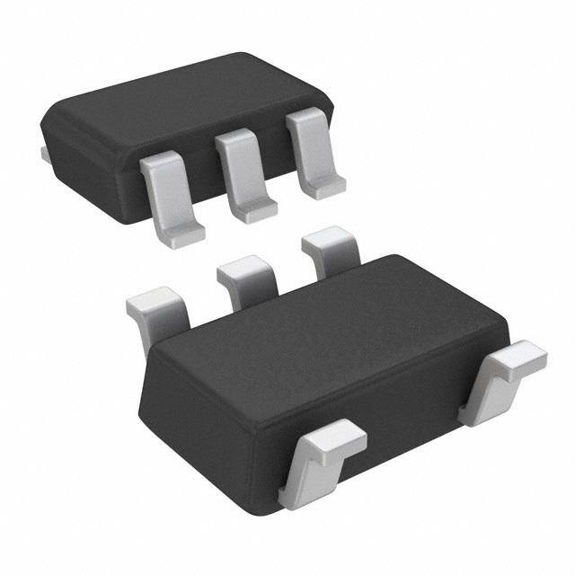
| 产品图片 |
|
| rohs | 符合RoHS无铅 / 符合限制有害物质指令(RoHS)规范要求 |
| 产品系列 | 放大器 IC,运算放大器 - 运放,STMicroelectronics TSV611ILT- |
| 数据手册 | |
| 产品型号 | TSV611ILT |
| 产品目录页面 | |
| 产品种类 | 运算放大器 - 运放 |
| 供应商器件封装 | SOT-23-5 |
| 共模抑制比—最小值 | 64 dB |
| 关闭 | No Shutdown |
| 其它名称 | 497-10350-2 |
| 其它有关文件 | http://www.st.com/web/catalog/sense_power/FM123/SC61/SS1613/LN1588/PF244675?referrer=70071840http://www.st.com/web/catalog/sense_power/FM123/SC61/SS1613/LN1591/PF244675?referrer=70071840 |
| 包装 | 带卷 (TR) |
| 压摆率 | 0.04 V/µs |
| 商标 | STMicroelectronics |
| 增益带宽生成 | 120 kHz |
| 增益带宽积 | 120kHz |
| 安装类型 | 表面贴装 |
| 安装风格 | SMD/SMT |
| 封装 | Reel |
| 封装/外壳 | SC-74A,SOT-753 |
| 封装/箱体 | SOT-23-5 |
| 工作温度 | -40°C ~ 85°C |
| 工作电源电压 | 1.5 V to 5.5 V |
| 工厂包装数量 | 3000 |
| 放大器类型 | 通用 |
| 最大工作温度 | + 85 C |
| 最小工作温度 | - 40 C |
| 标准包装 | 3,000 |
| 特色产品 | http://www.digikey.com/cn/zh/ph/ST/TVS61.html |
| 电压-电源,单/双 (±) | 1.5 V ~ 5.5 V |
| 电压-输入失调 | 4mV |
| 电流-电源 | 10.5µA |
| 电流-输入偏置 | 1pA |
| 电流-输出/通道 | 63mA |
| 电源电流 | 14 uA |
| 电路数 | 1 |
| 系列 | TSV611 |
| 转换速度 | 0.04 V/us |
| 输入偏压电流—最大 | 10 pA |
| 输入补偿电压 | 4 mV |
| 输出电流 | 63 mA |
| 输出类型 | 满摆幅 |
| 通道数量 | 1 Channel |


- 商务部:美国ITC正式对集成电路等产品启动337调查
- 曝三星4nm工艺存在良率问题 高通将骁龙8 Gen1或转产台积电
- 太阳诱电将投资9.5亿元在常州建新厂生产MLCC 预计2023年完工
- 英特尔发布欧洲新工厂建设计划 深化IDM 2.0 战略
- 台积电先进制程称霸业界 有大客户加持明年业绩稳了
- 达到5530亿美元!SIA预计今年全球半导体销售额将创下新高
- 英特尔拟将自动驾驶子公司Mobileye上市 估值或超500亿美元
- 三星加码芯片和SET,合并消费电子和移动部门,撤换高东真等 CEO
- 三星电子宣布重大人事变动 还合并消费电子和移动部门
- 海关总署:前11个月进口集成电路产品价值2.52万亿元 增长14.8%


PDF Datasheet 数据手册内容提取
TSV611, TSV611A, TSV612, TSV612A Rail-to-rail input/output 10 µA, 120 kHz CMOS operational amplifiers Datasheet - production data Applications • Battery-powered applications TSV611ILT - TSV611ICT • Smoke detectors • Proximity sensors IInn++ 11 55 VVCCCC++ VV 22 ++__ • Portable devices CCCC-- IInn-- 33 44 OOuutt • Signal conditioning SOT23-5/SC70-5 • Active filtering • Medical instrumentation Description TSV612IST - TSV612IDT The TSV61x family of single and dual operational OOuutt11 11 88 VV amplifiers offers low voltage, low power operation, CCCC++ and rail-to-rail input and output. IInn11-- 22 __ 77 OOuutt22 IInn11++ 33 ++ __ 66 IInn22-- The devices also feature an ultra-low input bias current as well as a low input offset voltage. VV 44 ++ 55 IInn22++ CCCC-- The TSV61x have a gain bandwidth product of 120 kHz while consuming only 10 µA at 5 V. MiniSO8/SO8 These features make the TSV61x family ideal for sensor interfaces, battery supplied and portable applications, as well as active filtering. Features • Rail-to-rail input and output • Low power consumption: 10 µA typ at 5 V • Low supply voltage: 1.5 to 5.5 V • Gain bandwidth product: 120 kHz typ • Unity gain stable • Low input offset voltage: 800 µV max (A version) • Low input bias current: 1 pA typ • Temperature range: -40 to 85 °C May 2017 DocID15768 Rev 3 1/21 This is information on a product in full production. www.st.com
Contents TSV611, TSV611A, TSV612, TSV612A Contents 1 Absolute maximum ratings and operating conditions . . . . . . . . . . . . . 3 2 Electrical characteristics . . . . . . . . . . . . . . . . . . . . . . . . . . . . . . . . . . . . . 4 3 Application information . . . . . . . . . . . . . . . . . . . . . . . . . . . . . . . . . . . . . 12 3.1 Operating voltages . . . . . . . . . . . . . . . . . . . . . . . . . . . . . . . . . . . . . . . . . . 12 3.2 Rail-to-rail input . . . . . . . . . . . . . . . . . . . . . . . . . . . . . . . . . . . . . . . . . . . . 12 3.3 Rail-to-rail output . . . . . . . . . . . . . . . . . . . . . . . . . . . . . . . . . . . . . . . . . . . 12 3.4 Driving resistive and capacitive loads . . . . . . . . . . . . . . . . . . . . . . . . . . . 13 3.5 PCB layouts . . . . . . . . . . . . . . . . . . . . . . . . . . . . . . . . . . . . . . . . . . . . . . . 13 3.6 Macromodel . . . . . . . . . . . . . . . . . . . . . . . . . . . . . . . . . . . . . . . . . . . . . . . 13 4 Package information . . . . . . . . . . . . . . . . . . . . . . . . . . . . . . . . . . . . . . . . 14 4.1 SOT23-5 package information . . . . . . . . . . . . . . . . . . . . . . . . . . . . . . . . . 15 4.2 SC70-5 (SOT323-5) package information . . . . . . . . . . . . . . . . . . . . . . . . 16 4.3 SO8 package information . . . . . . . . . . . . . . . . . . . . . . . . . . . . . . . . . . . . . 17 4.4 MiniSO8 package information . . . . . . . . . . . . . . . . . . . . . . . . . . . . . . . . . 18 5 Ordering information . . . . . . . . . . . . . . . . . . . . . . . . . . . . . . . . . . . . . . . 19 6 Revision history . . . . . . . . . . . . . . . . . . . . . . . . . . . . . . . . . . . . . . . . . . . 20 2/21 DocID15768 Rev 3
TSV611, TSV611A, TSV612, TSV612A Absolute maximum ratings and operating conditions 1 Absolute maximum ratings and operating conditions Table 1. Absolute maximum ratings Symbol Parameter Value Unit V Supply voltage (1) 6 CC V Differential input voltage (2) ±V V id CC V Input voltage (3) (V )- 0.2 to (V ) + 0.2 in CC- CC+ T Storage temperature -65 to 150 °C stg Thermal resistance junction to ambient (4) (5) SC70-5 205 R SOT23-5 250 °C/W thja MiniSO8 190 SO8 125 T Maximum junction temperature 150 °C j HBM: human body model (6) 4 kV ESD MM: machine model (7) 200 V CDM: charged device model (8) 1.5 kV Latch-up immunity 200 mA 1. All voltage values, except differential voltage are with respect to network ground terminal. 2. Differential voltages are the non-inverting input terminal with respect to the inverting input terminal. 3. Vcc-Vin must not exceed 6 V. 4. Short-circuits can cause excessive heating and destructive dissipation. 5. Rth are typical values. 6. Human body model: 100 pF discharged through a 1.5 kΩ resistor between two pins of the device, done for all couples of pin combinations with other pins floating. 7. Machine model: a 200 pF cap is charged to the specified voltage, then discharged directly between two pins of the device with no external series resistor (internal resistor < 5 Ω), done for all couples of pin combinations with other pins floating. 8. Charged device model: all pins plus package are charged together to the specified voltage and then discharged directly to ground. Table 2. Operating conditions Symbol Parameter Value Unit V Supply voltage 1.5 to 5.5 CC V V Common mode input voltage range (V )- 0.1 to (V ) + 0.1 icm CC- CC+ T Operating free air temperature range -40 to 85 °C oper DocID15768 Rev 3 3/21 21
Electrical characteristics TSV611, TSV611A, TSV612, TSV612A 2 Electrical characteristics Table 3. Electrical characteristics at V = 1.8 V with V = 0 V, V = V /2, CC+ CC- icm CC T = 25 °C, and R connected to V /2 (unless otherwise specified) amb L CC Symbol Parameter Conditions Min. Typ. Max. Unit DC performance TSV61x 4 TSV61xA 0.8 V Offset voltage mV io T < T < T TSV61x 5 min. op max. T < T < T TSV61xA 2 min. op max ∆Vio/∆T Input offset voltage drift 2 μV/°C Input offset current 1 10 (1) I io (Vout = Vcc/2) Tmin. < Top < Tmax. 1 100 pA Input bias current 1 10 (1) I ib (Vout = Vcc/2) Tmin. < Top < Tmax. 1 100 Common mode rejection 0 V to 1.8 V, Vout = 0.9 V 55 71 CMR ratio 20 log (ΔVic/ΔVio) Tmin. < Top < Tmax. 53 R = 10 kΩ, Vout = 0.5 V to dB L 78 83 A Large signal voltage gain 1.3 V vd T < T < T 74 min. op max. High level output voltage R = 10 kΩ 4 35 V L OH (VOH = VCC - Vout) Tmin. < Top < Tmax. 50 mV R = 10 kΩ 7 35 V Low level output voltage L OL Tmin. < Top < Tmax. 50 V = 1.8 V 9 13 Isink o T < T < T 9 min. op max. I mA out V = 0 V 8 10 Isource o T < T < T 8 min. op max. Supply current No load, Vout = Vcc/2 6.5 9 12 I µA CC (per operator) T < T < T 6 12.5 min. op max. AC performance GBP Gain bandwidth product 100 kHz φm Phase margin R = 10 kΩ, C = 20 pF 60 Degrees L L G Gain margin 9.5 dB m R = 10 kΩ, C = 20 pF, SR Slew rate L L 0.03 V/μs V = 0.5 V to 1.3 V out 4/21 DocID15768 Rev 3
TSV611, TSV611A, TSV612, TSV612A Electrical characteristics Table 3. Electrical characteristics at V = 1.8 V with V = 0 V, V = V /2, CC+ CC- icm CC T = 25 °C, and R connected to V /2 (unless otherwise specified) (continued) amb L CC Symbol Parameter Conditions Min. Typ. Max. Unit Equivalent input noise en voltage f = 1 kHz 110 ---n--H-V---z--- F = 1 kHz, Av = 1, Total harmonic distortion + in THD+N V = 1 V R = 100 kΩ, 0.07 % noise out pp, L BW = 22 kHz 1. Guaranteed by design. DocID15768 Rev 3 5/21 21
Electrical characteristics TSV611, TSV611A, TSV612, TSV612A Table 4. Electrical characteristics at V = 3.3 V, V = 0 V, V = V /2, CC+ CC- icm CC T = 25 °C, R connected to V /2 (unless otherwise specified) amb L CC Symbol Parameter Min. Typ. Max. Unit DC performance TSV61x 4 TSV61xA 0.8 V Offset voltage mV io T <T <T TSV61x 5 min op max T <T <T TSV61xA 2 min op max ∆Vio/∆T Input offset voltage drift 2 μV/°C 1 10 (1) I Input offset current io T < T < T 1 100 min. op max. pA 1 10 (1) I Input bias current ib T < T < T 1 100 min. op max. Common mode rejection 0 V to 3.3 V, Vout = 1.75 V 61 76 CMR ratio 20 log (ΔVic/ΔVio) Tmin. < Top < Tmax. 58 R = 10 kΩ, Vout = 0.5 V to dB L 85 92 A Large signal voltage gain 2.8 V vd T < T < T 83 min. op max. High level output voltage R = 10 kΩ 5 35 V L OH (VOH = VCC - Vout) Tmin. < Top < Tmax. 50 mV R = 10 kΩ 10 35 V Low level output voltage L OL Tmin. < Top < Tmax. 50 V = V 37 44 Isink o CC T < T < T 35 min. op max. I mA out V = 0 V 32 38 Isource o T < T < T 30 min. op max. Supply current No load, Vout = VCC/2 6.5 9.5 12.5 I µA CC (per operator) T < T < T 6 13 min. op max. AC performance GBP Gain bandwidth product 110 kHz φm Phase margin R = 10 kΩ, C = 20 pF 60 Degrees L L G Gain margin 9.5 dB m R = 10 kΩ, C = 20 pF, SR Slew rate L L 0.035 V/μs V = 0.5V to 2.8V out Equivalent input noise en voltage f = 1 kHz 110 ---n--H-V---z--- 1. Guaranteed by design. 6/21 DocID15768 Rev 3
TSV611, TSV611A, TSV612, TSV612A Electrical characteristics T able 5. Electrical characteristics at V = 5 V, V = 0 V, V = V /2, T = 25 °C, CC+ CC- icm CC amb R connected to V /2 (unless otherwise specified) L CC Symbol Parameter Min. Typ. Max. Unit DC performance TSV61x 4 TSV61xA 0.8 V Offset voltage mV io T <T <T TSV61x 5 min op max T <T <T TSV61xA 2 min op max ∆Vio/∆T Input offset voltage drift 2 μV/°C 1 10 (1) I Input offset current io T < T < T 1 100 min. op max. pA 1 10 (1) I Input bias current ib T < T < T 1 100 min. op max. Common mode rejection 0 V to 5 V, Vout = 2.5 V 64 80 CMR ratio 20 log (ΔVic/ΔVio) Tmin. < Top < Tmax. 63 Supply voltage rejection Vcc = 1.8 to 5 V 76 93 SVR ratio 20 log (ΔVcc/ΔVio) Tmin. < Top < Tmax. 74 dB R = 10 kΩ, Vout = 0.5 V to L 88 93 A Large signal voltage gain 4.5 V vd T <T <T 85 min op max High level output voltage R = 10 kΩ 7 35 V L OH (VOH = VCC - Vout) Tmin. < Top < Tmax. 50 mV R = 10 kΩ 16 35 V Low level output voltage L OL Tmin. < Top < Tmax. 50 V = V 52 57 Isink o CC T < T < T 42 min. op max. I mA out V = 0 V 58 63 Isource o T < T < T 49 min. op max. Supply current No load, Vout = VCC/2 7.5 10.5 14 I µA CC (per operator) T < T < T 7 15 min. op max. AC performance GBP Gain bandwidth product 120 kHz φm Phase margin R = 10 kΩ, C = 20 pF 62 Degrees L L G Gain margin 10 dB m R = 10 kΩ, C = 20 pF, V SR Slew rate L L out 0.04 V/μs = 0.5V to 4.5V DocID15768 Rev 3 7/21 21
Electrical characteristics TSV611, TSV611A, TSV612, TSV612A Table 5. Electrical characteristics at V = 5 V, V = 0 V, V = V /2, T = 25 °C, CC+ CC- icm CC amb R connected to V /2 (unless otherwise specified) (continued) L CC Symbol Parameter Min. Typ. Max. Unit Equivalent input noise en voltage f = 1 kHz 105 ---n--H-V----z-- F = 1 kHz, Av = 1, Total harmonic distortion + in THD+N V = 1 V R = 100 kΩ, 0.02 % noise out pp, L BW = 22kHz 1. Guaranteed by design. 8/21 DocID15768 Rev 3
TSV611, TSV611A, TSV612, TSV612A Electrical characteristics Figure 1. Supply current vs. supply voltage at Figure 2. Output current vs. output voltage at V = V /2 V = 1.5 V icm CC CC Figure 3. Output current vs. output voltage at Figure 4. Voltage gain and phase vs. frequency V = 5 V at V = 1.5 V CC CC n (dB) margin (°) Gai se a h P Figure 5. Voltage gain and phase vs. frequency Figure 6. Phase margin vs. output current at V = 5 V CC B) gin(°) n (d mar Gai se a h P DocID15768 Rev 3 9/21 21
Electrical characteristics TSV611, TSV611A, TSV612, TSV612A Figure 7. Positive slew rate vs. time, V = 1.5 V, Figure 8. Negative slew rate vs. time, V = 1.5 V, CC CC C = 100 pF, R = 10 kΩ C = 100 pF, R = 10 kΩ Load Load Load Load V =1.5V, V =V /2, CC icm CC T=85°C R =10kΩ, C =100pF Load Load V =V /2 Load CC V) T=−40°C de ( T=-40°C u plit T=25°C m A T=85°C V =1.5V, V =V /2 CC icm CC R =10kΩ, C =100pF Load Load T=25°C Time (µs) Time (µs) Figure 9. Positive slew rate vs. time, V = 5.5 V, Figure 10. Negative slew rate vs. time, V = 5.5 V, CC CC C = 100 pF, R = 100 kΩ C = 100 pF, R = 100 kΩ Load Load Load Load Ω Ω Figure 11. Slew rate vs. supply voltage Figure 12. Noise vs. frequency at Vcc = 5 V z) H V V/ n y ( sit n e d e s oi Vicm=2.5V n nt e al v ui q e put V =5V Vicm=4.5V n CC I T=25°C Frequency (Hz) 10/21 DocID15768 Rev 3
TSV611, TSV611A, TSV612, TSV612A Electrical characteristics Figure 13. Distortion + noise vs. frequency Figure 14. Distortion + noise vs. output voltage 1 Vcc=1.5V %) Vcc=1.5V N (%) Rl=10kΩ + N ( Rl=10kohms + 0.1 D Vcc=1.5V HD Vcc=1.5V TH Rl=100kohms T Rl=100kΩ Vcc=5.5V f=1kHz Rl=10kohms Gain=1 Ω Vcc=5.5V BW=22kHz Rl=100kohms Vicm=Vcc/2 0.01 Ω 10 100 1000 10000 Output Voltage (Vpp) Figure 15. Voltage gain and phase vs. frequency Figure 16. Voltage gain and phase vs. frequency at V = 1.8 V (based on simulation results) at V = 5 V (based on simulation results) CC CC n (dB) margin (°) n (dB) margin (°) Gai se Gai se a a h h P P DocID15768 Rev 3 11/21 21
Application information TSV611, TSV611A, TSV612, TSV612A 3 Application information 3.1 Operating voltages The TSV61x can operate from 1.5 to 5.5 V. The parameters are fully specified for 1.8, 3.3, and 5 V power supplies. However, the parameters are very stable in the full V range and CC several characterization curves show the TSV61x characteristics at 1.5 V. Additionally, the main specifications are guaranteed in extended temperature ranges from -40 °C to 85 °C. 3.2 Rail-to-rail input The TSV61x are built with two complementary PMOS and NMOS input differential pairs. The devices have a rail-to-rail input, and the input common mode range is extended from (V ) - 0.1 V to (V ) + 0.1 V. The transition between the two pairs appears at CC- CC+ (V ) - 0.7 V. In the transition region, the performance of CMRR, PSRR, V and THD is CC+ io slightly degraded (as shown in Figure 17 and Figure 18 for V vs. V ). io icm Figure 17. Input offset voltage vs input common Figure 18. Input offset voltage vs input common mode at V = 1.5 V mode at V = 5 V CC CC 11..55 11..44 11..22 11..00 11..00 V) V) 00..88 m m ge ( 00..55 ge ( 00..66 Volta 00..00 Volta 0000....2244 ut Offset --00..55 ut Offset --0000....2200 p p --00..44 n n I --11..00 I --00..66 --00..88 --11..55 --11..00 00..00 00..22 00..44 00..66 00..88 11..00 11..22 11..44 00..00 11..00 22..00 33..00 44..00 55..00 Input Common Mode Voltage (V) Input Common Mode Voltage (V) The device is guaranteed without phase reversal. 3.3 Rail-to-rail output The operational amplifiers’ output levels can go close to the rails: less than 35 mV above GND rail and less than 35 mV below V rail when connected to 10 kΩ load to V /2. CC CC 12/21 DocID15768 Rev 3
TSV611, TSV611A, TSV612, TSV612A Application information 3.4 Driving resistive and capacitive loads These products are micro-power, low-voltage operational amplifiers optimized to drive rather large resistive loads, above 10 kΩ. For lower resistive loads, the THD level may significantly increase. In a follower configuration, these operational amplifiers can drive capacitive loads up to 100 pF with no oscillations. When driving larger capacitive loads, adding an in-series resistor at the output can improve the stability of the devices (see Figure 19 for recommended in-series resistor values). Once the in-series resistor value has been selected, the stability of the circuit should be tested on bench and simulated with the simulation model. Figure 19. In-series resistor vs. capacitive load Ω) (or st si e s r e eri s n- I 3.5 PCB layouts For correct operation, it is advised to add 10 nF decoupling capacitors as close as possible to the power supply pins. 3.6 Macromodel An accurate macromodel of the TSV61x is available on STMicroelectronics’ web site at www.st.com. This model is a trade-off between accuracy and complexity (that is, time simulation) of the TSV61x operational amplifiers. It emulates the nominal performances of a typical device within the specified operating conditions mentioned in the datasheet. It also helps to validate a design approach and to select the right operational amplifier, but it does not replace on-board measurements. DocID15768 Rev 3 13/21 21
Package information TSV611, TSV611A, TSV612, TSV612A 4 Package information In order to meet environmental requirements, ST offers these devices in different grades of ECOPACK® packages, depending on their level of environmental compliance. ECOPACK® specifications, grade definitions and product status are available at: www.st.com. ECOPACK® is an ST trademark. 14/21 DocID15768 Rev 3
TSV611, TSV611A, TSV612, TSV612A Package information 4.1 SOT23-5 package information Figure 20. SOT23-5 package outline Table 6. SOT23-5 mechanical data Dimensions Ref. Millimeters Inches Min. Typ. Max. Min. Typ. Max. A 0.90 1.20 1.45 0.035 0.047 0.057 A1 0.15 0.006 A2 0.90 1.05 1.30 0.035 0.041 0.051 B 0.35 0.40 0.50 0.013 0.015 0.019 C 0.09 0.15 0.20 0.003 0.006 0.008 D 2.80 2.90 3.00 0.110 0.114 0.118 D1 1.90 0.075 e 0.95 0.037 E 2.60 2.80 3.00 0.102 0.110 0.118 F 1.50 1.60 1.75 0.059 0.063 0.069 L 0.10 0.35 0.60 0.004 0.013 0.023 K 0 degrees 10 degrees DocID15768 Rev 3 15/21 21
Package information TSV611, TSV611A, TSV612, TSV612A 4.2 SC70-5 (SOT323-5) package information Figure 21. SC70-5 (SOT323-5) package outline SIDE VIEW DIMENSIONS IN MM GAUGE PLANE COPLANAR LEADS SEATING PLANE TOP VIEW Table 7. SC70-5 (SOT323-5) mechanical data Dimensions Ref Millimeters Inches Min Typ Max Min Typ Max A 0.80 1.10 0.315 0.043 A1 0.10 0.004 A2 0.80 0.90 1.00 0.315 0.035 0.039 b 0.15 0.30 0.006 0.012 c 0.10 0.22 0.004 0.009 D 1.80 2.00 2.20 0.071 0.079 0.087 E 1.80 2.10 2.40 0.071 0.083 0.094 E1 1.15 1.25 1.35 0.045 0.049 0.053 e 0.65 0.025 e1 1.30 0.051 L 0.26 0.36 0.46 0.010 0.014 0.018 < 0° 8° 16/21 DocID15768 Rev 3
TSV611, TSV611A, TSV612, TSV612A Package information 4.3 SO8 package information Figure 22. SO8 package outline Table 8. SO8 mechanical data Dimensions Ref. Millimeters Inches Min. Typ. Max. Min. Typ. Max. A 1.75 0.069 A1 0.10 0.25 0.004 0.010 A2 1.25 0.049 b 0.28 0.48 0.011 0.019 c 0.17 0.23 0.007 0.010 D 4.80 4.90 5.00 0.189 0.193 0.197 E 5.80 6.00 6.20 0.228 0.236 0.244 E1 3.80 3.90 4.00 0.150 0.154 0.157 e 1.27 0.050 h 0.25 0.50 0.010 0.020 L 0.40 1.27 0.016 0.050 L1 1.04 0.040 k 1° 8° 1° 8° ccc 0.10 0.004 DocID15768 Rev 3 17/21 21
Package information TSV611, TSV611A, TSV612, TSV612A 4.4 MiniSO8 package information Figure 23. MiniSO8 package outline Table 9. MiniSO8 mechanical data Dimensions Ref. Millimeters Inches Min. Typ. Max. Min. Typ. Max. A 1.1 0.043 A1 0 0.15 0 0.006 A2 0.75 0.85 0.95 0.030 0.033 0.037 b 0.22 0.40 0.009 0.016 c 0.08 0.23 0.003 0.009 D 2.80 3.00 3.20 0.11 0.118 0.126 E 4.65 4.90 5.15 0.183 0.193 0.203 E1 2.80 3.00 3.10 0.11 0.118 0.122 e 0.65 0.026 L 0.40 0.60 0.80 0.016 0.024 0.031 L1 0.95 0.037 L2 0.25 0.010 k 0° 8° 0° 8° ccc 0.10 0.004 18/21 DocID15768 Rev 3
TSV611, TSV611A, TSV612, TSV612A Ordering information 5 Ordering information Table 10. Order codes Temperature Order code Package Packing Marking range TSV611ILT K12 SOT23-5 TSV611AILT K11 TSV611ICT K12 SC70-5 TSV611AICT K11 -40 °C to 85 °C Tape and reel TSV612IDT V612I SO-8 TSV612AIDT V612AI TSV612IST K113 MiniSO-8 TSV612AIST K115 DocID15768 Rev 3 19/21 21
Revision history TSV611, TSV611A, TSV612, TSV612A 6 Revision history T able 11. Document revision history Date Revision Changes 28-May-2009 1 Initial release. Full datasheet for product now in production. 18-Jan-2010 2 Added Figure 1 to Figure 19. Table 3, Table 4, and Table 5: changed “DVio to ∆Vio/∆T, updated VOH parameter information, changed min. values of 11-May-2017 3 VOH parameter to max. values. Table 10: Order codes: removed obsolete order codes TSV612ID and TSV612AID 20/21 DocID15768 Rev 3
TSV611, TSV611A, TSV612, TSV612A IMPORTANT NOTICE – PLEASE READ CAREFULLY STMicroelectronics NV and its subsidiaries (“ST”) reserve the right to make changes, corrections, enhancements, modifications, and improvements to ST products and/or to this document at any time without notice. Purchasers should obtain the latest relevant information on ST products before placing orders. ST products are sold pursuant to ST’s terms and conditions of sale in place at the time of order acknowledgement. Purchasers are solely responsible for the choice, selection, and use of ST products and ST assumes no liability for application assistance or the design of Purchasers’ products. No license, express or implied, to any intellectual property right is granted by ST herein. Resale of ST products with provisions different from the information set forth herein shall void any warranty granted by ST for such product. ST and the ST logo are trademarks of ST. All other product or service names are the property of their respective owners. Information in this document supersedes and replaces information previously supplied in any prior versions of this document. © 2017 STMicroelectronics – All rights reserved DocID15768 Rev 3 21/21 21