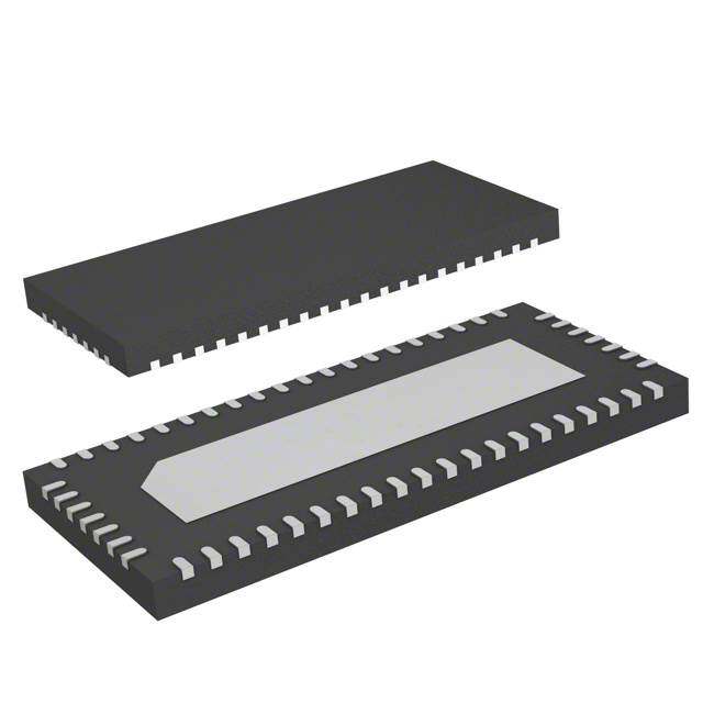
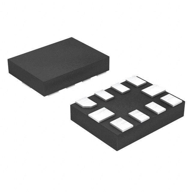
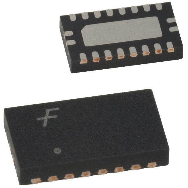
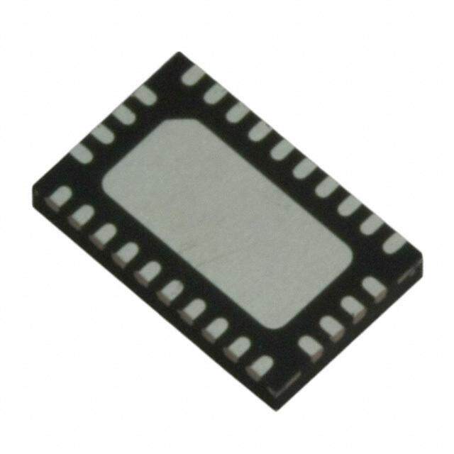
ICGOO在线商城 > 集成电路(IC) > 接口 - 模拟开关 - 专用 > TSU6712YFPRB
- 型号: TSU6712YFPRB
- 制造商: Texas Instruments
- 库位|库存: xxxx|xxxx
- 要求:
| 数量阶梯 | 香港交货 | 国内含税 |
| +xxxx | $xxxx | ¥xxxx |
查看当月历史价格
查看今年历史价格
TSU6712YFPRB产品简介:
ICGOO电子元器件商城为您提供TSU6712YFPRB由Texas Instruments设计生产,在icgoo商城现货销售,并且可以通过原厂、代理商等渠道进行代购。 TSU6712YFPRB价格参考。Texas InstrumentsTSU6712YFPRB封装/规格:接口 - 模拟开关 - 专用, 检测 开关 IC 1 通道 25-DSBGA(2x2)。您可以下载TSU6712YFPRB参考资料、Datasheet数据手册功能说明书,资料中有TSU6712YFPRB 详细功能的应用电路图电压和使用方法及教程。
| 参数 | 数值 |
| 产品目录 | 集成电路 (IC)半导体 |
| 描述 | IC USB SWITCH SP4T 25DSBGAUSB开关IC SP4T Switch w/ Impedance Detection |
| 产品分类 | |
| 品牌 | Texas Instruments |
| 产品手册 | |
| 产品图片 |
|
| rohs | 符合RoHS无铅 / 符合限制有害物质指令(RoHS)规范要求 |
| 产品系列 | 开关 IC,USB开关IC,Texas Instruments TSU6712YFPRB- |
| 数据手册 | |
| 产品型号 | TSU6712YFPRB |
| 产品培训模块 | http://www.digikey.cn/PTM/IndividualPTM.page?site=cn&lang=zhs&ptm=26070 |
| 产品种类 | USB开关IC |
| 供应商器件封装 | 25-DSBGA(2x2) |
| 其它名称 | 296-28762-1 |
| 制造商产品页 | http://www.ti.com/general/docs/suppproductinfo.tsp?distId=10&orderablePartNumber=TSU6712YFPRB |
| 功能 | |
| 包装 | 剪切带 (CT) |
| 商标 | Texas Instruments |
| 安装类型 | 表面贴装 |
| 安装风格 | SMD/SMT |
| 导通电阻 | 5.5 欧姆 |
| 导通电阻—最大值 | 5.5,15,18 Ohms |
| 封装 | Reel |
| 封装/外壳 | 25-XFBGA,CSPBGA |
| 封装/箱体 | DSBGA-25 |
| 工作温度 | -40°C ~ 85°C |
| 工作温度范围 | - 40 C to + 85 C |
| 工厂包装数量 | 3000 |
| 带宽 | 510 MHz |
| 开关数量 | Quad |
| 开关电流—典型值 | +/- 60 mA |
| 开关配置 | SP4T |
| 最大工作温度 | + 85 C |
| 最小工作温度 | - 40 C |
| 标准包装 | 1 |
| 电压-电源,单/双 (±) | 1.65 V ~ 3.6 V |
| 电压源 | 单电源 |
| 电流-电源 | - |
| 电源电压-最大 | 28 V |
| 电源电压-最小 | - 0.5 V |
| 电源电流 | 30 uA |
| 电路 | 1 x SP4T |
| 空闲时间—最大值 | 4.5 us |
| 系列 | TSU6712 |
| 运行时间—最大值 | 120 us |


PDF Datasheet 数据手册内容提取
TSU6712 www.ti.com SCDS321A–MAY2011–REVISEDJULY2013 SP4T SWITCH WITH IMPEDANCE DETECTION MICRO-USB SWITCH TO SUPPORT USB, UART, AUDIO, AND VIDEO CheckforSamples:TSU6712 FEATURES 1 • DetectionisCompatibletoCEA-936A(4-Wire RVCPACKAGE Protocol,UARTInterface) (TOPVIEW) • USBPathSupportsUSB2.0HighSpeed 1 2 3 4 5 • SupportControlSignals(USB,UARTJIG) UsedinManufacturing(JIG,BOOT) A INTB VDDIO ISET OUT VBUS • InterruptforAttachandDetachAccessory • CompatibleAccessories – USBCable,UARTCable,TVOutCable B D + SDA S_L MIC DM – Mono,StereoHeadset – RemoteControllerforDMB – Charging+TVOut C D - SCL V_L S_R DP – Charging+StereoHeadset • ESDPerformanceTestedPerJESD22 – 1500-VHuman-BodyModel D VBAT IDBP V_R VIDEO ID (A114-B,ClassII) – 1000-VCharged-DeviceModel(C101) • ESDPerformanceDP/DM/ID/VBUStoGND E RxD TxD BOOT JIG GND – ±6-kVContactDischarge(IEC61000-4-2) APPLICATIONS DESCRIPTION • CellPhones&SmartPhones The TSU6712 is a multiple SP4T switch with • TabletPCs impedance detection. The switch features impedance • DigitalCameras&Camcorders detection, which supports the detection of various accessories that are attached through DP and DM. • GPSNavigationSystems The detection is based on the impedance values of • MicroUSBinterfacewith the accessories as defined in Table 1. The TSU6712 USB/UART/Audio/Video is fully controlled using I2C and enables USB data, stereo and mono audio, video, microphone, and UARTdatatouseacommonconnectorport. Power for this device is supplied through VBAT of the system or through VBUS when attached. The switch can be controlled through I2C. JIG and BOOT pins are used when a USB, UART JIG cable is used to testduringdevelopmentandmanufacturing. ORDERINGINFORMATION Forthemostcurrentpackageandorderinginformation,seethePackageOptionAddendumattheendofthis document,orseetheTIwebsiteatwww.ti.com 1 Pleasebeawarethatanimportantnoticeconcerningavailability,standardwarranty,anduseincriticalapplicationsof TexasInstrumentssemiconductorproductsanddisclaimerstheretoappearsattheendofthisdatasheet. PRODUCTIONDATAinformationiscurrentasofpublicationdate. Copyright©2011–2013,TexasInstrumentsIncorporated Products conform to specifications per the terms of the Texas Instruments standard warranty. Production processing does not necessarilyincludetestingofallparameters.
TSU6712 SCDS321A–MAY2011–REVISEDJULY2013 www.ti.com APPLICATIONBLOCKDIAGRAM VVDDDDIIOO XXllaattoorrss SSCCLL CClloocckk LLooaadd SSoouurrcceess SSwwiittcchheess SSwwiittcchh SSDDAA SSeennssee OOUUTT && CCttrrll.. II22CC IInntteerrffaaccee IINNTTBB SSww.. && DD++ CChhgg.. SSttaattee RReeggiisstteerrss JJIIGG DD-- PPuummpp MMaacchhiinnee BBOOOOTT IIDDBBPP VV__LL IISSEETT VVIIDDEEOO SS__LL BBuuffffeerrss aanndd//oorr SS__RR CCoommppaarraattoorrss MMIICC VVBBUUSS DDPP UART Buffer DDMM TTxxDD IIDD VVBBAATT CChhaarrggeerr SSuuppeerrvviissoorr DDeetteeccttiioonn AAcccceessssoorryy AAnndd VVPPOOWWEERR((aallllcckkttss)) SSoouurrcceess IIDD PPwwrr.. SSeell.. RReesseett RRxxDD DDeetteeccttiioonn aanndd AADDCC CCoommpp’’ss.. AAVVSSSS 2 SubmitDocumentationFeedback Copyright©2011–2013,TexasInstrumentsIncorporated
TSU6712 www.ti.com SCDS321A–MAY2011–REVISEDJULY2013 TERMINALFUNCTIONS TERMINAL I/O DESCRIPTION BallNO. NAME D1 VBAT – 3.0–4.4VBatterysupplyvoltage A2 VDDIO – 1.8~3.3VLogicSupply A5 VBUS I USBconnectorVBUS A4 OUT O Phonechargeroutput E5 GND – Ground B1 D+ I/O USBdata+ C1 D- I/O USBdata- D2 IDBP I/O USBIDdata E1 RxD I/O UARTreceivedata E2 TxD I/O UARTtransmitdata D3 V_R I/O TV-outrightsound C3 V_L I/O TV-outleftsound D4 VIDEO I/O TV-outencodedvideo B4 MIC I/O Microphonesignal C4 S_R I/O Stereoheadsetrightsound B3 S_L I/O Monoorstereoheadsetleftsound C2 SCL I I2Cclock B2 SDA I/O I2Cdata C5 DP I/O CommonI/Oport B5 DM I/O CommonI/Oport D5 ID I/O CommonI/Oport A1 INTB O Processorinterruptsignalwhenperipheralisplugged/unplugged.Push-pulloutput A3 ISET O Fast-modechargeroutput.Open-drainoutput E4 JIG O GPIOfactoryoutput.Open-drainoutput E3 BOOT O GPIOfactoryoutput.Push-pulloutput Copyright©2011–2013,TexasInstrumentsIncorporated SubmitDocumentationFeedback 3
TSU6712 SCDS321A–MAY2011–REVISEDJULY2013 www.ti.com ABSOLUTE MAXIMUM RATINGS(1) (2) overoperatingfree-airtemperaturerange(unlessotherwisenoted) MIN MAX UNIT V SupplyvoltagefromUSBconnector –0.5 28 BUS V V Supplyvoltagefrombattery -0.5 6 BAT V Logicsupplyvoltage -0.5 4.6 V DDIO OUT Phonechargeroutput -0.5 7 V V AudioSwitch -1.5 V +0.5 AUDIO BAT V MicSwitch -0.5 V +0.5 MICIO BAT V VIDEOI SwitchI/Ovoltagerange VideoSwitch -1 V +0.5 V BAT O V UARTBuffer -0.5 4.6 UARTIO V USBSwitch -0.5 V +0.5 USBIO BAT V Voltageappliedtologicoutput(SCL,SDA,INTB,ISET,BOOT,JIG) -0.5 4.6 V LOGIC I PeakinputcurrentonV pin 2 A BUS BUS I PeakoutputcurrentonOUTpin 2 A OUT I Analogportdiodecurrent -50 50 mA K I ON-statecontinuousswitchcurrent -60 60 mA SW-DC I SW- ON-statepeakswitchcurrent -150 150 mA PEAK I Digitallogicinputclampcurrent V <0 -50 mA IK L I Continuouscurrentthroughlogicoutput -50 50 mA LOGIC_O I ContinuouscurrentthroughGND 100 mA GND T Storagetemperaturerange –65 150 °C stg (1) Stressesabovetheseratingsmaycausepermanentdamage.Exposuretoabsolutemaximumconditionsforextendedperiodsmay degradedevicereliability.Thesearestressratingsonly,andfunctionaloperationofthedeviceattheseoranyotherconditionsbeyond thosespecifiedisnotimplied. (2) Thealgebraicconvention,wherebythemostnegativevalueisaminimumandthemostpositivevalueisamaximum. THERMAL IMPEDANCE RATINGS UNIT θ Packagethermalimpedance YFPpackage 98.8 °C/W JA RECOMMENDED OPERATING CONDITIONS overoperatingfree-airtemperaturerange(unlessotherwisenoted) Condition Min Max Units V 4.0 6.5 V BUS V 3.0 4.4 V BAT V 1.8 3.3 V DDIO USB_I/O 0 3.6 V UART_I/O 0 2.7 V Video_I/O -0.5 2 V Audio_I/O -0.8 0.8 V MIC_I/O 0 2.3 V Temperature -40 85 ˚C 4 SubmitDocumentationFeedback Copyright©2011–2013,TexasInstrumentsIncorporated
TSU6712 www.ti.com SCDS321A–MAY2011–REVISEDJULY2013 DIGITAL SIGNALS – I2C INTERFACE AND GPIO overoperatingfree-airtemperaturerange(unlessotherwisenoted) TESTCONDITIONS MIN MAX UNIT V LogicandI/Osupplyvoltage 1.65 3.6 V DDIO V High-levelinputvoltage V ×0.7 V V IH DDIO DDIO V Low-levelinputvoltage 0 V ×0.3 V IL DDIO V High-leveloutputvoltage I =-3mA V ×0.7 V OH OH DDIO V Low-leveloutputvoltage I =3mA 0 0.4 V OL OL f SCLfrequency 400 kHz SCL UART BUFFER overoperatingfree-airtemperaturerange(unlessotherwisenoted) PARAMETER TESTCONDITIONS MIN MAX UNIT FromPhoneTransmittertoAccessory V High-levelinputvoltage(TxD) V =2.8V 1.15 V V IH DDIO DDIO V Low-levelinputvoltage(TxD) V =2.8V 0 0.49 V IL DDIO V High-leveloutputvoltage(DP,DM) I =–4mA,V =3.0V 2.4 V V OH OH BAT BAT V Low-leveloutputvoltage(DP,DM) I =4mA,V =3.0V 0 0.55 V OL OL BAT FromAccessorytoPhoneReceiver V High-levelinputvoltage(DP,DM) V =3.0V 2.0 V V IH BAT BAT V Low-levelinputvoltage(DP,DM) V =3.0V 0 0.8 V IL BAT V High-leveloutputvoltage(RxD) I =–4mA,V =2.8V 1.16 V V OH OH DDIO DDIO V Low-leveloutputvoltage(RxD) I =4mA,V =2.8V 0 0.33 V OL OL DDIO JIG AND ISET FAST-MODE CHARGER OUTPUT (OPEN-DRAIN OUTPUT) overoperatingfree-airtemperaturerange(unlessotherwisenoted) PARAMETER TESTCONDITIONS MIN MAX UNIT V Low-leveloutputvoltage I =10mA,V =3.0V 0.5 V OL OL BAT INTB AND BOOT (PUSH-PULL OUTPUT) overoperatingfree-airtemperaturerange(unlessotherwisenoted) PARAMETER TESTCONDITIONS MIN MAX UNIT V High-leveloutputvoltage I =–4mA,V =2.8V 2.2 V V OH OH DDIO DDIO V Low-leveloutputvoltage I =4mA,V =2.8V 0 0.33 V OL OL DDIO Copyright©2011–2013,TexasInstrumentsIncorporated SubmitDocumentationFeedback 5
TSU6712 SCDS321A–MAY2011–REVISEDJULY2013 www.ti.com OVP ELECTRICAL CHARACTERISTICS overoperatingfree-airtemperaturerange(unlessotherwisenoted) PARAMETER SYMBOL TESTCONDITIONS MIN TYP MAX UNIT In Undervoltagelockout,input V increasingfrom0Vto5V,Noload powerdetectedthreshold V BUS 2.65 2.8 3 V UVLO+ onOUTpin rising Undervoltagelockout,input V decreasingfrom5Vto0V,Noload powerdetectedthreshold V BUS 2.25 2.44 2.7 V UVLO– onOUTpin falling HysteresisonUVLO V ΔofV andV 150 260 550 mV HYS-UVLO UVLO+ UVLO– InputtoOutputCharacteristics V switchresistance R V =5V,I =100mA 120 200 mΩ BUS DS-VBUSSWITCH BUS OUT Turn-ONtime t R =36Ω,C =400pF 16 ms ON L L Turn-OFFtime t R =36Ω,C =400pF 50 μs OFF L L InputOvervoltageProtection(OVP) Inputovervoltage V V V increasingfrom6Vto8V 6.8 7 7.2 V protectionthreshold BUS OVP BUS MaximumOVdelay V t 0.25 1 µs BUS PD(OVP) HysteresisonOVP V V V decreasingfrom8Vto6V 25 100 300 mV BUS HYS-UVLO BUS Recoverytimefrom TimemeasuredfromV 8V≥6V,1-μs inputovervoltage V t BUS 8 ms BUS ON(OVP) fall-time condition TOTAL SWITCH CURRENT CONSUMPTION overoperatingfree-airtemperaturerange(unlessotherwisenoted) PARAMETER SYMBOL TESTCONDITIONS MIN TYP MAX UNIT VBATStandbyCurrent I V =0V 30 µA Consumption BAT(Standby) BUS VBATOperatingCurrent I V =0V 150 µA Consumption BAT(Operating) BUS VBUSOperatingCurrent I NoloadonOUTpin,V =5V 150 600 µA Consumption VBUS BUS 6 SubmitDocumentationFeedback Copyright©2011–2013,TexasInstrumentsIncorporated
TSU6712 www.ti.com SCDS321A–MAY2011–REVISEDJULY2013 AUDIO SWITCH ELECTRICAL CHARACTERISTICS(1) V =3Vto4.4V,V =2.8V,T =–40°Cto85°C(unlessotherwisenoted) BAT DDIO A PARAMETER SYMBOL TESTCONDITIONS MIN TYP MAX UNIT AnalogSwitch Analogsignalrange V –0.8 0.8 V AUDIO S_LorS_R, ON-stateresistance r V =±0.8V,I =–20mA,V =3.F0V 2 5.5 Ω DMorDP ON I O BAT ON-stateresistance S_LorS_R, Δr V =0.8V,I =–20mA,V =3.0V 0.05 0.5 Ω matchbetweenchannels DMorDP ON I I BAT ON-stateresistance S_LorS_R, r V =±0.8V,I =–20mA,V =3.0V 0.05 0.2 Ω flatness DMorDP ON(flat) I O BAT (V =0V,V =0.8V)or(V =0.8V, V orV OFFleakagecurrent I I O I 200 500 nA I O IO(OFF) V =–0.8V),V =4.4V,SwitchOFF O BAT V =OPEN,V =–0.8Vor0.8V, V ONleakagecurrent I I O 10 300 nA O IO(ON) V =4.4V,SwitchON BAT Dynamic Fromreceipt Turn-ONtime ofI2Cstop t V orV =V ,R =50Ω,C =35pF 120 µs ON I O BAT L L bit Fromreceipt Turn-OFFtime ofI2Cstop t V orV =V ,R =50Ω,C =35pF 4.5 µs OFF I O BAT L L bit DCbias=0Vor1.6V,f=10MHz, V OFFcapacitance C 5.5 pF I I(OFF) SwitchOFF DCbias=0Vor1.6V,f=10MHz, V OFFcapacitance C 10 pF O O(OFF) SwitchOFF C , DCbias=0Vor1.6V V,V ONcapacitance I(ON) 13 pF I O C f=10MHz,SwitchON O(ON) Bandwidth BW R =50Ω,SwitchON 450 MHz L OFFIsolation O f=20kHz,R =50Ω,SwitchOFF –100 dB ISO L Crosstalk X f=20kHz,R =50Ω –85 dB TALK L R =16Ω,C =20pF,f=20Hzto20kHz, Totalharmonicdistortion THD L L 0.05 % 1.6-V output pp (1) V isequaltotheassertedvoltageonS_RandS_Lpins.V isequaltotheassertedvoltageonDPandDMpins.I isequaltothe I O I currentontheS_RandS_Lpins.I isequaltothecurrentontheDPandDMpins. O Copyright©2011–2013,TexasInstrumentsIncorporated SubmitDocumentationFeedback 7
TSU6712 SCDS321A–MAY2011–REVISEDJULY2013 www.ti.com MIC SWITCH ELECTRICAL CHARACTERISTICS (1) V =3Vto4.4V,V =2.8V,T =–40°Cto85°C(unlessotherwisenoted) BAT DDIO A PARAMETER SYMBOL TESTCONDITIONS MIN TYP MAX UNIT AnalogSwitch Analogsignalrange V 0 2.3 V MICIO ON-stateresistance MIC,V r V =2.3V,I =–2mA,V =3V 40 70 Ω BUS ON I O BAT V =0.3V,V =2.3V I O or V orV OFFleakagecurrent I 5 500 nA I O IO(OFF) V =2.3V,V =0.3V, I O V =4.4V,SwitchOFF BAT V =OPEN,V =1.35V,V =4.4V, MICpulldownresistance R I O BAT 1.5 kΩ PD(ON) SwitchON Dynamic Fromreceipt Turn-ONtime ofI2CACK t V orV =V ,R =50Ω,C =35pF 120 µs ON I O BAT L L bit Fromreceipt Turn-OFFtime ofI2CACK t V orV =V ,R =50Ω,C =35pF 11 µs OFF I O BAT L L bit DCbias=0Vor3.6V,f=10MHz, V OFFcapacitance C 140 pF I I(OFF) SwitchOFF DCbias=0Vor3.6V,f=10MHz, V OFFcapacitance C 10.5 pF O O(OFF) SwitchOFF C , DCbias=0Vor3.6V,f=10MHz, V,V ONcapacitance I(ON) 140 pF I O C SwitchON O(ON) Bandwidth BW R =50Ω,SwitchON 40 MHz L OFFIsolation O f=20kHz,R =50Ω,SwitchOFF –95 dB ISO L Crosstalk X f=20kHz,R =50Ω,toaudiooutput –85 dB TALK L RL=600Ω,CL=20pF,f=20Hz–20 Totalharmonicdistortion THD 0.46 0.65 % kHz,V =0.1V centeredatV /2 in pp BAT (1) V isequaltotheassertedvoltageonV pin.V isequaltotheassertedvoltageonMICpin.I isequaltothecurrentontheV pin. I BUS O I BUS I isequaltothecurrentontheMICpin. O 8 SubmitDocumentationFeedback Copyright©2011–2013,TexasInstrumentsIncorporated
TSU6712 www.ti.com SCDS321A–MAY2011–REVISEDJULY2013 VIDEO SWITCH ELECTRICAL CHARACTERISTICS(1) V =3.0Vto4.4V,V =2.8V,T =–40°Cto85°C(unlessotherwisenoted) BAT DDIO A PARAMETER SYMBOL TESTCONDITIONS MIN TYP MAX UNIT AnalogSwitch Analogsignalrange V –0.5 2 V VIDEOIO V_L,V_R,or V =0.5Vto2V,I =–20mA,V =3.0 ON-stateresistance VIDEO r I O BAT 12 18 Ω ON V DM,DP,orID ON-stateresistance V_L,V_R matchbetween Δr V =1.0V,I =–2.0mA,V =3.0V 0.5 2 Ω DM,DP ON I I BAT channels ON-stateresistance V_L,V_R V =0.5Vto2.0V,I =–20mA,V =3.0 r I O BAT 0.5 2 Ω flatness DM,DP ON(flat) V V =0.3V,V =2.0V I O or V orV OFFleakagecurrent I 60 360 nA I O IO(OFF) V =2V,V =0.3V, I O V =4.4V,SwitchOFF BAT V =OPEN,V =0.3Vor2.0V, V ONleakagecurrent I I O 60 360 nA O IO(ON) V =4.4V,SwitchON BAT Dynamic Fromreceiptof Turn-ONtime I2CACKbit tON VIorVO=VBAT,RL=50Ω,CL=35pF 70 µs Fromreceiptof Turn-OFFtime I2CACKbit tOFF VIorVO=VBAT,RL=50Ω,CL=35pF 26 µs DCbias=0Vor3.6V,f=10MHz, V OFFcapacitance C 3 pF I I(OFF) SwitchOFF DCbias=0Vor3.6V,f=10MHz, V OFFcapacitance C 10 pF O O(OFF) SwitchOFF C , DCbias=0Vor3.6V,f=10MHz, V,V ONcapacitance I(ON) 12 pF I O C SwitchON O(ON) Bandwidth BW R =50Ω,SwitchON 450 MHz L f=10MHz,R =50Ω, OFFIsolation O L(VIDEO) –58 dB ISO SwitchOFF f=10MHz,R =50Ω, Crosstalk X L(VIDEO) –60 dB TALK SwitchON Totalharmonic R =600Ω,C =20pF,f=20Hz~20kHz, V_LorV_R THD L L 0.05 % distortion 2.3V output pp (1) V isequaltotheassertedvoltageonDP,DM,andIDpins.V isequaltotheassertedvoltageonD+,D–,andIDBPpins.I isequalto O I O thecurrentontheDP,DM,andIDpins.I isequaltothecurrentontheD+,D–,andIDBPpins. I Copyright©2011–2013,TexasInstrumentsIncorporated SubmitDocumentationFeedback 9
TSU6712 SCDS321A–MAY2011–REVISEDJULY2013 www.ti.com USB SWITCH ELECTRICAL CHARACTERISTICS(1) V =3Vto4.4V,V =2.8V,T =–40°Cto85°C(unlessotherwisenoted) BAT DDIO A PARAMETER SYMBOL TESTCONDITIONS MIN TYP MAX UNIT AnalogSwitch Analogsignalrange V 0 V V USBIO BAT D–,D+,orIDBP ON-stateresistance r V =0Vto3.6V,I =–2mA,V =3V 8 15 Ω DM,DP,orID ON I O BAT ON-stateresistance D–,D+ matchbetween Δr V =0.4V,I =–2mA,V =3V 0.5 1 Ω DM,DP ON I O BAT channels ON-stateresistance D–,D+ r V =0Vto3.6V,I =–2mA,V =3V 0.5 1 Ω flatness DM,DP ON(flat) I O BAT V =0.3V,V =2.7V I O or V orV OFFleakagecurrent I 45 360 nA I O IO(OFF) V =2.7V,V =0.3V, I O V =4.4V,SwitchOFF BAT V =OPEN,V =0.3Vor2.7V, V ONleakagecurrent I I O 50 360 nA O IO(ON) V =4.4V,SwitchON BAT Dynamic Fromreceiptof Turn-ONtime I2CACKbit tON VIorVO=VBAT,RL=50Ω,CL=35pF 95 µs Fromreceiptof Turn-OFFtime I2CACKbit tOFF VIorVO=VBAT,RL=50Ω,CL=35pF 25 µs DCbias=0Vor3.6V,f=10MHz, V OFFcapacitance C 3 pF I I(OFF) SwitchOFF DCbias=0Vor3.6V,f=10MHz, V OFFcapacitance C 10 pF O O(OFF) SwitchOFF C , DCbias=0Vor3.6V,f=10MHz, V,V ONcapacitance I(ON) 11 pF I O C SwitchON O(ON) Bandwidth BW R =50Ω,SwitchON 510 MHz L OFFIsolation O f=240MHz,R =50Ω,SwitchOFF –24 dB ISO L Crosstalk X f=240MHz,R =50Ω –40 dB TALK L (1) V isequaltotheassertedvoltageonDP,DM,andIDpins.V isequaltotheassertedvoltageonD+,D–,andIDBPpins.I isequalto O I O thecurrentontheDP,DM,andIDpins.I isequaltothecurrentontheD+,D–,andIDBPpins. I 10 SubmitDocumentationFeedback Copyright©2011–2013,TexasInstrumentsIncorporated
TSU6712 www.ti.com SCDS321A–MAY2011–REVISEDJULY2013 GENERAL OPERATION The TSU6712 will automatically detect accessories plugged into the phone via the mini USB 5 pin connector. The type of accessory detected will be stored in I2C registers within the TSU6712 for retrieval by the host. The TSU6712 has a network of switches that can be automatically opened and closed base on the accessory detection. See Table 1 for details of which switches are open during each mode of operation. For flexibility, the TSU6712 also offers a manual switching mode allowing the host processor to decide which switches should be openedandclosedandexecutethesettingsthroughtheI2Cinterface. Standby Mode Standbymodeisthedefaultmodeuponpowerupandoccurswhennoaccessoryhasbeendetected.Duringthis mode, the VBUS and ID lines are continually monitored through comparators to determine when an accessory is inserted.Powerconsumptionisminimalduringstandbymode. Accessory ID Detection If VBUS is high and the attachment is not a charger, then determine the impedance on the ID pin. If VBUS is low and an accessory is attached, then use an ADC for impedance sensing on the ID pin to identify which accessory isattachedand/orwhatkindofremotecontrolkeybuttonispushed. Impedance Buckets for Each Accessory and Remote Control Key Button In order to implement ID detection, each accessory and remote control key button of audio accessory should containbelowIDimpedanceresistorvaluewhichis1%toleranceaccuracy. OVP OPERATION The device continuously monitors the input voltage and the input current as described in detail in the following sections. InputOvervoltageProtection When the input voltage rises above V , the internal V switch is turned off, removing power from the circuit. OVP BUS The response is very rapid, with the FET switch turning off in less than 1 µs. The OVP_EN interrupt bit is set high when an overvoltage condition is detected. When the input voltage returns below V – V and OVP HYS-OVP remains above V , the V FET switch is turned on again after a deglitch time of t . The deglitch time UVLO BUS ON(OVP) ensures that the input supply has stabilized before turning the switch on. When the OVP condition is cleared, the OVP_OCP_DISinterruptbitissethigh. OVPGlitchImmunity When V is near the OVP threshold, noise on V cause spurious OVP triggering. To avoid this, OVP glitch BUS BUS immunityallowsnoiseontheV linetoberejected.Theglitchprotectioncircuitryintegratestheglitchovertime BUS allowing the OVP circuitry to trigger faster for larger voltage excursions above the OVP threshold and slower for shorterexcursions.TheprotectioncircuitryhasamaximumOVdelayof1µs Copyright©2011–2013,TexasInstrumentsIncorporated SubmitDocumentationFeedback 11
TSU6712 SCDS321A–MAY2011–REVISEDJULY2013 www.ti.com AV Cable Detection Once an A/V cable is attached with 365 kΩ ID resistance and/or 75 Ω load resistance, the ID voltage will drop below the internal comparator reference level of the TSU6712 and the ADC block of the TSU6712 will determine theIDlineimpedancevalue.TheIDdetectsignalthatissenttothelogiccontrolblockwillbesetequaltoanA/V cable accessory. With the video driver in the phone enabled, detection block of the TSU6712 will sense that the 75ohm load resistance at the end of the A/V cable is still attached since the video sync pulse will always be present. Power-On Reset When power (from 0 V) is applied to V , an internal power-on reset holds the TSU6712 in a reset condition BAT until V has reached V . At that point, the reset condition is released, and the TSU6712 registers and I2C BAT POR statemachineinitializetotheirdefaultstates. After the initial power-up phase, V must be lowered to below 0.2 V and then back up to the operating voltage BAT (V )forapower-resetcycle. DDIO Software Reset The TSU6712 has software reset feature. Hold low both SCL and SDA more than 30ms will reset digital logic of theTSU6712.Afterresetting,INTBwillkeeplowuntilINT_MaskbitofControlregister(0x02)iscleared. Key Press Identification Key Key PressTiming Long Key PressTiming INTB Key Press Interrupt Long Key Press Interrupt Long Key Release Interrupt (A) (B) (C) A. Keypress B. Releasedkeypress→SetKPInterrupt→SeterrorbitinButtonregister→INTBpulledlow C. I2CreadofINTregister→ClearKPinterrupt→INTBgoesbackhigh Figure1. ShortKeyPress 12 SubmitDocumentationFeedback Copyright©2011–2013,TexasInstrumentsIncorporated
TSU6712 www.ti.com SCDS321A–MAY2011–REVISEDJULY2013 Key Key PressTiming Long Key PressTiming INTB Key Press Interrupt Long Key Press Interrupt Long Key Release Interrupt (A) (B) (C) A. Keypress B. Releasedkeypress→SetKPInterrupt→SetKey(S/E,1–12)bitinButtonregister→INTBpullledlow C. I2CreadofINTregister→ClearKPinterrupt→INTBgoesbackhigh Figure2. NormalKeyPress Key Key PressTiming Long Key PressTiming INTB Key Press Interrupt Long Key Press Interrupt Long Key Release Interrupt (A) (B) (C) (D) (E) A. Keypress B. Longkeypresstimingreached→SetLKPinterruptbit→SetKey(S/E,1–12)bitinButtonregister→INTBpullled low C. I2CreadofINTregister→ClearLKPinterruptbit→INTBgoesbackhigh D. Releasedkeypress→SetLKRInterruptbit→INTBpullledlow E. I2CreadofINTregister→ClearLKRinterruptbit→INTBgoesbackhigh Figure3. LongKeyPress Copyright©2011–2013,TexasInstrumentsIncorporated SubmitDocumentationFeedback 13
TSU6712 SCDS321A–MAY2011–REVISEDJULY2013 www.ti.com Key Key PressTiming Long Key PressTiming INTB Key Press Interrupt Stuck Key Press Interrupt Stuck Key Release Interrupt (A) (B) (C) (D) (E) A. Keypressdetectedwhenaccessoryattached B. Longkeypresstimingreached→SetSKinterruptbit→SetKey(S/E,1–12)bitinButtonregister→INTBpullledlow C. I2CreadofINTregister→ClearSKinterruptbit→INTBgoesbackhigh D. ReleasedkeypressdetectedwhenaccessoryIDresistoris1MΩ→SetSKRInterruptbit→INTBpullledlow E. I2CreadofINTregister→ClearSKRinterruptbit→INTBgoesbackhigh Figure4. StuckKeyPress RSend_End R1 R2 R3 R4 R5 R6 R7 R8 R9 R10 R11 R12 Send_End S1 S2 S3 S4 S5 S6 S7 S8 S9 S10 S11 S12 R ID Hold Figure5. Audio/RemoteControllerAccessory 14 SubmitDocumentationFeedback Copyright©2011–2013,TexasInstrumentsIncorporated
TSU6712 www.ti.com SCDS321A–MAY2011–REVISEDJULY2013 Table1.AccessoryDetectionScheme 1%IDResistorTolerance(ResistorValuesandPartNumbers) IDRESISTOR DETECTED ACCCESSORY VALUEON IMPEDANCEON ADCVALUE ACCESSORY TSU6712 OTG – – 00000 Send_EndButton 2K 2K 00001 StereoHeadsetwithRCS1Button 0.604K 2.604K 00010 StereoHeadsetwithRCS2Button 0.604K 3.208K 00011 StereoHeadsetwithRCS3Button 0.806K 4.014K 00100 StereoHeadsetwithRCS4Button 0.806K 4.82K 00101 StereoHeadsetwithRCS5Button 1.21K 6.03K 00110 StereoHeadsetwithRCS6Button 2K 8.03K 00111 StereoHeadsetwithRCS7Button 2K 10.03K 01000 StereoHeadsetwithRCS8Button 2K 12.03K 01001 StereoHeadsetwithRCS9Button 2.43K 14.46K 01010 StereoHeadsetwithRCS10Button 2.8K 17.26K 01011 StereoHeadsetwithRCS11Button 3.24K 20.5K 01100 StereoHeadsetwithRCS12Button 3.57K 24.07K 01101 AudioDeviceType3 28.7K 28.7K 01110 ReservedAccessory#2 34K 34K 01111 ReservedAccessory#4 49.9K 49.9K 10001 ReservedAccessory#5 64.9K 64.9K 10010 AudioDeviceType2 56.2K 80.27K 10011 PhonePoweredDevice 102K 102K 10100 TTYConverter 121K 121K 10101 UARTCable 150K 150K 10110 Type1Charger 200K 200K 10111 FactoryModeCable–BootOffUSB 255K 255K 11000 FactoryModeCable–BootOnUSB 301K 301K 11001 Audio/VideoCable 365K 365K 11010 Type2Charger 442K 442K 11011 FactoryModeCable–BootOffUART 523K 523K 11100 FactoryModeCable–BootOnUART 619K 619K 11101 StereoHeadsetwithRemote(AudioDeviceType1) 976K 1000.07K 11110 Mono/StereoHeadset(AudioDeviceType1) 1000K 1002K 11110 NoDevice – – 11111 Standard I2C Interface Details The bidirectional I2C bus consists of the serial clock (SCL) and serial data (SDA) lines. Both lines must be connected to a positive supply via a pullup resistor when connected to the output stages of a device. Data transfermaybeinitiatedonlywhenthebusisnotbusy. I2C communication with this device is initiated by the master sending a START condition, a high-to-low transition on the SDA input/output while the SCL input is high (see Figure 6). After the start condition, the device address byte is sent, MSB first, including the data direction bit (R/W). This device does not respond to the general call address. After receiving the valid address byte, this device responds with an ACK, a low on the SDA input/output duringthehighoftheACK-relatedclockpulse. Copyright©2011–2013,TexasInstrumentsIncorporated SubmitDocumentationFeedback 15
TSU6712 SCDS321A–MAY2011–REVISEDJULY2013 www.ti.com SDA SCL S P Start Condition Stop Condition Figure6. DefinitionofSTARTandSTOPConditions The data byte follows the address ACK. The R/W bit is kept low for transfer from the master to the slave. The data byte is followed by an ACK sent from this device. Data are output only if complete bytes are received and acknowledged. The output data is valid at time (tpv) after the low-to-high transition of SCL, during the clock cycle fortheACK. On the I2C bus, only one data bit is transferred during each clock pulse. The data on the SDA line must remain stable during the high pulse of the clock period, as changes in the data line at this time are interpreted as control commands(STARTorSTOP)(seeFigure7). SDA SCL Data Line Change Figure7. BitTransfer A Stop condition, a low-to-high transition on the SDA input/output while the SCL input is high, is sent by the master(seeFigure6). Thenumberofdatabytestransferredbetweenthestartandthestopconditionsfromtransmittertoreceiverisnot limited. Each byte of eight bits is followed by one ACK bit. The transmitter must release the SDA line before the receivercansendanACKbit. A slave receiver that is addressed must generate an ACK after the reception of each byte. The device that acknowledgeshastopulldowntheSDAlineduringtheACKclockpulsesothattheSDAlineisstablelowduring thehighpulseoftheACK-relatedclockperiod(seeFigure8).Setupandholdtimesmustbetakenintoaccount. Data Output by Transmitter NACK Data Output by Receiver ACK SCLFrom Master 1 2 8 9 S Start Clock Pulse for Condition Acknowledgment Figure8. AcknowledgmentonI2CBus 16 SubmitDocumentationFeedback Copyright©2011–2013,TexasInstrumentsIncorporated
TSU6712 www.ti.com SCDS321A–MAY2011–REVISEDJULY2013 Writes Data is transmitted to the TSU6712 by sending the device slave address and setting the LSB to a logic 0 (see Figure 9 for device address). The command byte is sent after the address and determines which register receives the data that follows the command byte. The next byte is written to the specified register on the rising edgeoftheACKclockpulse. SCL 1 2 3 4 5 6 7 8 9 SlaveAddress Command Byte Data to Register MSB LSB SDA S 0 1 0 0 1 0 1 0 A 0 0 0 0 0 0 1 1/0 A Data A P Start Condition R/W ACK From Slave ACK From Slave ACK From Slave Figure9. WritetoRegister Reads The bus master first must send the TSU6712 slave address with the LSB set to a logic 0. The command byte is sent after the address and determines which register is accessed. After a restart, the device slave address is sent again but, this time, the LSB is set to a logic 1. Data from the register defined by the command byte then is sent by the TSU6712. Data is clocked into the SDA output shift register on the rising edge of the ACK clock pulse.SeeFigure10. ACK From ACK From ACK From NACK From SlaveAddress Slave Slave SlaveAddress Slave Data from Register Master MSB LSB S 0 1 0 0 1 0 1 0 A Command Byte A S 0 1 0 0 1 0 1 1 A Data NA P R/W At this moment, master-transmitter R/W First byte becomes master-receiver, and slave-receiver becomes slave transmitter Figure10. ReadFromRegister ClearINTRegistersUponRead The TSU6712 I2C logic core is set to clear all INT bits in a register after that register is read by the host. When the acknowledge is received from the Master after the INT register has been read, the contents of the register is resettothedefaultstate. I2CTiming SCL Slave Address Sub Address Date Byte Date Byte SDA ST 0 1 0 0 1 0 1 0 A 0 0 0 0 0 0 1 0 A D7 D6 D5 D4 D3 D2 D1 D0 A D7 D6 D5 D4 D3 D2 D1 D0 A SP Start W/R Register Address ACK Data to Control ACK Data to Control ACK Stop ACK From Slave (Control Reg) From Register From Register From Auto-Inc. Slave Slave Slave Figure11.RepeatedDataWritetoaSingleRegister Copyright©2011–2013,TexasInstrumentsIncorporated SubmitDocumentationFeedback 17
TSU6712 SCDS321A–MAY2011–REVISEDJULY2013 www.ti.com SlaveAddress SubAddress Date Byte Date Byte SDA ST 0 1 0 0 1 0 1 0 A 1 0 0 0 1 0 0 0 A D7 D6 D5 D4 D3 D2 D1 D0 A D7 D6 D5 D4 D3 D2 D1 D0 A Start W/R RegisterAddress ACK Data to Timing Set 1 ACK Data to Timing Set 2 ACK ACK From Slave (Timing Set 1 Reg) From Register From Register From Auto-Inc. Slave Slave Slave Figure12.BurstDataWritetoMultipleRegisters SlaveAddress SubAddress SlaveAddress Date Byte SDA ST 0 1 0 0 1 0 1 0 A 0 0 0 0 0 0 1 1 A RS 0 1 0 0 1 0 1 1 A D7 D6 D5 D4 D3 D2 D1 D0 Data from Interrupt 1 Reg. Start W/R RegisterAddress ACKRe-Start W/R ACK From Slave (Interrupt 1 Reg) From ACK From Slave Auto-Inc. Slave Date Byte Date Byte continued A D7 D6 D5 D4 D3 D2 D1 D0 A D7 D6 D5 D4 D3 D2 D1 D0NASP Data from Interrupt 1 Reg. Data from Interrupt 1 Reg. Stop ACK From Master ACK From Master NoACK From Master(Message Ends) Figure13.RepeatedDataReadfromaSingleRegister– CombinedMode SCL SlaveAddress SubAddress SlaveAddress Date Byte SDA ST 0 1 0 0 1 0 1 0 A 1 0 0 0 0 0 1 1 A RS 0 1 0 0 1 0 1 1 A D7 D6 D5 D4 D3 D2 D1 D0 Data from Interrupt 1 Reg. Start W/R RegisterAddress ACKRe-Start W/R ACK From Slave (Interrupt 1 Reg) From ACK From Slave Auto-Inc. Slave Date Byte Date Byte continued A D7 D6 D5 D4 D3 D2 D1 D0 A D7 D6 D5 D4 D3 D2 D1 D0NASP Data from Interrupt 2 Reg. Data fromIntMask 1 Reg. Stop ACK From Master ACK From Master NoACK From Master (Message Ends) Figure14.BurstDataReadfromMultipleRegisters– CombinedMode SlaveAddress SubAddress SlaveAddress Date Byte SDA ST 0 1 0 0 1 0 1 0 A 0 0 0 0 0 0 1 1 A SP ST 0 1 0 0 1 0 1 1 A D7 D6 D5 D4 D3 D2 D1 D0 Data from Interrupt 1 Reg. Start W/R RegisterAddress ACK Start W/R ACK From Slave (Interrupt 1 Reg) FromStop ACK From Slave Auto-Inc. Slave Continued Date Byte Date Byte continued A D7 D6 D5 D4 D3 D2 D1 D0 A D7 D6 D5 D4 D3 D2 D1 D0NASP Data from Interrupt 1 Reg. Data from Interrupt 1 Reg. Stop ACK From Master ACK From Master NoACK From Master (Message Ends) Figure15.RepeatedDataReadfromaSingleRegister– SplitMode 18 SubmitDocumentationFeedback Copyright©2011–2013,TexasInstrumentsIncorporated
TSU6712 www.ti.com SCDS321A–MAY2011–REVISEDJULY2013 SCL SlaveAddress SubAddress SlaveAddress Date Byte SDA ST 0 1 0 0 1 0 1 0 A 1 0 0 0 0 0 1 1 A SP ST 0 1 0 0 1 0 1 1 A D7 D6 D5 D4 D3 D2 D1 D0 Data from Interrupt 1 Reg. Start W/R RegisterAddress ACK Start W/R ACK From Slave (Interrupt 1 Reg) From Stop ACK From Slave Auto-Inc. Slave Continued Date Byte Date Byte continued A D7 D6 D5 D4 D3 D2 D1 D0 A D7 D6 D5 D4 D3 D2 D1 D0NASP Data from Interrupt 2 Reg. Data fromIntMask 1 Reg. Stop ACK From Master ACK From Master NoACK From Master(Message Ends) Figure16.BurstDataReadfromMultipleRegisters– SplitMode A. SDAispulledlowonACKfromslaveorACKfrommaster. B. Registerwritesalwaysrequiresub-addresswritebeforefirstdatabyte. C. Repeateddatawritestoasingleregistercontinueindefinitelyuntilstoporrestart. D. RepeateddatareadsfromasingleregistercontinueindefinitelyuntilnoACKfrommaster. E. Burstdatawritesstartatthespecifiedregisteraddress,thenadvancetothenextregisteraddress,eventotheread- only registers. For these registers, data write appears to occur, though no data are changed by the writes. After register14hiswritten,writingresumestoregister01handcontinuesuntilstoporrestart. F. Burstdatareadsstartatthespecifiedregisteraddress,thenadvancetothenextregisteraddress.Onceregister14h isread,readingresumesfromregister01handcontinuesuntilNoACKfrommaster. Copyright©2011–2013,TexasInstrumentsIncorporated SubmitDocumentationFeedback 19
TSU6712 SCDS321A–MAY2011–REVISEDJULY2013 www.ti.com I2CRegisterMap(1)(2)(3) RESET ADDR REGISTER TYPE BIT7 BIT6 BIT5 BIT4 BIT3 BIT2 BIT1 BIT0 VALUE 01h DeviceID R 01010010 VersionID VendorID 02h Control R/W xxx11111 SwitchOpen RawData ManualS/W Wait INTMask 03h Interrupt1 R 00000000 OVP_OCP_DIS OCP_EN OVP_EN LKR LKP KP Detach Attach Stuck_Key_R Reserved 04h Interrupt2 R x0000000 OTP_EN CONNECT Stuck_Key ADC_Change A/V_Charging CV _Attach Interrupt 05h R/W 00000000 OVP_OCP_DIS OCP_EN OVP_EN LKR LKP KP Detach Attach Mask1 Interrupt Stuck_Key Reserved 06h R/W x0000000 OTP_EN CONNECT Stuck_Key ADC_Change A/V_Charging Mask2 _RCV _Attach 07h ADC R xxx11111 ADCValue 08h TimingSet1 R/W 00000000 KeyPress DeviceWakeUp 09h TimingSet2 R/W 00000000 SwitchingWait LongKeyPress DeviceType 0Ah R 00000000 USBOTG DCP CDP UART USB AudioType2 AudioType1 1 DeviceType JIG_UART JIG_UART JIG_USB 0Bh R 00000000 AudioType3 A/V TTY PPD JIG_USB_ON 2 _OFF _ON _OFF 0Ch Button1 R 00000000 7 6 5 4 3 2 1 Send_End 0Dh Button2 R x0000000 Unknown Error 12 11 10 9 8 UnusedInt 0Fh 1(4) R 00000000 UnusedInt 10h 2(4) R xxxx0000 UnusedInt 11h Mask1(4) R/W 00000000 UnusedInt 12h Mask2(4) R/W xxxx0000 13h ManualS/W1 R/W 00000000 D–Switching D+Switching VBUSSwitching 14h ManualS/W2 R/W xxx00000 ChargerDET BOOT_SW JIG-ON IDSwitching (1) Donotuseblankregisterbits. (2) Write"0"totheblankregisterbits. (3) Valuesreadfromtheblankregisterbitsarenotdefinedandinvalid. (4) Inordertopreventunusedinterruptsfrominterferingwithnormaloperation,itisadvisedtowrite‘FFh’toReg.11hand‘0Fh’toReg.12h onstart-up.Otherwise,Reg.0Fhand10hmustbereadtoclearaninterruptifReg.03hand04hhavebeenreadandcontaindata‘00h’ Table2.SlaveAddress DESCRIPTION NAME SIZE(BITS) BIT7 BIT6 BIT5 BIT4 BIT3 BIT2 BIT1 BIT0 Slaveaddress 8 0 1 0 0 1 0 1 R/W 20 SubmitDocumentationFeedback Copyright©2011–2013,TexasInstrumentsIncorporated
TSU6712 www.ti.com SCDS321A–MAY2011–REVISEDJULY2013 DeviceID Address: 01h ResetValue: 01010010 Type: Read SIZE BITNO. NAME DESCRIPTION (BITS) 0-2 VersionID 4 Auniquenumberforvendor010bforTexasInstruments 4-7 VendorID 5 Auniquenumberforchipversion01010bforTSU6712 Control Address: 02h ResetValue: xxx11111 Type: Read/Write SIZE BITNO. NAME DESCRIPTION (BITS) 0:Unmaskinterrupt 0 INTMask 1 1:Maskinterrupt 0:Waituntilhostre-setsthisbit(WAITbit)high 1 Wait 1 1:WaituntilSwitchingtimerisexpireddefinedinTimingSet1 0:ManualSwitching 2 ManualS/W 1 1:AutomaticSwitching 0:ReportthestatuschangesonIDtoHost 3 RAWData 1 1:Don'treportthestatuschangesonID 0:OpenallSwitches(Includingloadswitch) 4 SwitchOpen 1 1:AutomaticSwitchingbyaccessorystatus 5-7 Unused 3 Copyright©2011–2013,TexasInstrumentsIncorporated SubmitDocumentationFeedback 21
TSU6712 SCDS321A–MAY2011–REVISEDJULY2013 www.ti.com Interrupt1 Address: 03h ResetValue: 00000000 Type: ReadandClear SIZE BITNO. NAME DESCRIPTION (BITS) 0 Attach 1 1:Accessoryisattached 1 Detach 1 1:Accessoryisdetached 2 KP 1 1:Keypress 3 LKP 1 1:Longkeypress 4 LKR 1 1:Longkeyrelease 5 OVP_EN 1 1:OVPenabled 6 OCP_EN 1 1:OCPenabled 7 OVP_OCP_DIS 1 1:OVP_OCPdisabled Interrupt2 Address: 04h ResetValue: x0000000 Type: ReadandClear SIZE BITNO. NAME DESCRIPTION (BITS) 0 A/V_Charging 1 1:ChargerdetectedwhenA/Vcableisattached 1 Reserved_Attach 1 1:ReservedDeviceisattached 2 ADC_Change 1 1:ADCvalueischangedwhenRAWdataisenabled 3 Stuck_Key 1 1:StuckKeyisdetected 4 Stuck_Key_RCV 1 1:StuckKeyisrecovered 5 Connect 1 1:Switchisconnected(closed) 6 OTP_EN 1 1:OverTemperatureProtectionenabled 7 Unused 1 22 SubmitDocumentationFeedback Copyright©2011–2013,TexasInstrumentsIncorporated
TSU6712 www.ti.com SCDS321A–MAY2011–REVISEDJULY2013 InterruptMask1 Address: 05h ResetValue: 00000000 Type: ReadandClear SIZE BITNO. NAME DESCRIPTION (BITS) 0:UnmaskAttachInterrupt 0 Attach 1 1:MaskAttachInterrupt 1:MaskDetachInterrupt 1 Detach 1 0:UnmaskKeypressInterrupt 0:UnmaskKeypressInterrupt 2 KP 1 1:MaskKeypressInterrupt 0:UnmaskLongkeypressInterrupt 3 LKP 1 1:MaskLongkeypressInterrupt 0:UnmaskLongkeyreleaseInterrupt 4 LKR 1 1:MaskLongkeyreleaseInterrupt 0:UnmaskOVP_ENInterrupt 5 OVP_EN 1 1:MaskOVP_ENInterrupt 0:UnmaskOCP_ENInterrupt 6 OCP_EN 1 1:MaskOCP_ENInterrupt 0:UnmaskOVP_OCP_DISInterrupt 7 OVP_OCP_DIS 1 1:MaskOVP_OCP_DISInterrupt Copyright©2011–2013,TexasInstrumentsIncorporated SubmitDocumentationFeedback 23
TSU6712 SCDS321A–MAY2011–REVISEDJULY2013 www.ti.com InterruptMask2 Address: 06h ResetValue: x0000000 Type: ReadandClear SIZE BITNO. NAME DESCRIPTION (BITS) 0:UnmaskA/V_ChargingInterrupt 0 A/V_Charging 1 1:MaskA/V_ChargingInterrupt 0:UnmaskReserved_AttachInterrupt 1 Reserved_Attach 1 1:MaskReserved_AttachInterrupt 0:UnmaskADC_ChangeInterrrupt 2 ADC_Change 1 1:MaskADC_ChangeInterrrupt 0:UnmaskStuck_KeyInterrupt 3 Stuck_Key 1 1:MaskStuck_KeyInterrupt 0:UnmaskStuck_Key_RCVInterrupt 4 Stuck_Key_RCV 1 1:MaskStuck_Key_RCVInterrupt 0:UnmaskConnectInterrupt 5 Connect 1 1:MaskConnectInterruptt 0:UnmaskOTP_ENInterrupt 6 OTP_EN 1 1:MaskOTP_ENInterrupt 7 Unused 1 ADCValue Address: 07h ResetValue: xxx11111 Type: Read SIZE BITNO. NAME DESCRIPTION (BITS) 0-4 ADCvalue 5 ADCvaluereadfromID 5-7 N/A 3 24 SubmitDocumentationFeedback Copyright©2011–2013,TexasInstrumentsIncorporated
TSU6712 www.ti.com SCDS321A–MAY2011–REVISEDJULY2013 TimingSet1 Address: 08h ResetValue: 00000000 Type: Read/Write SIZE BITNO. NAME DESCRIPTION (BITS) 0-3 Devicewakeup 4 Devicewakeupduration 4-7 Keypress 4 Normalkeypressduration TimingSet2 Address: 09h ResetValue: 00000000 Type: Read/Write SIZE BITNO. NAME DESCRIPTION (BITS) 0-3 Longkeypress 4 Longkeypressduration 4-7 Switchingwait 4 Waitingdurationbeforeswitching Table3.TimeTable SETTING DEVICE LONG SWITCHING KEYPRESS VALUE WAKEUP KEYPRESS WAIT 0000 50ms 100ms 300ms 10ms 0001 100ms 200ms 400ms 30ms 0010 150ms 300ms 500ms 50ms 0011 200ms 400ms 600ms 70ms 0100 300ms 500ms 700ms 90ms 0101 400ms 600ms 800ms 110ms 0110 500ms 700ms 900ms 130ms 0111 600ms 800ms 1000ms 150ms 1000 700ms 900ms 1100ms 170ms 1001 800ms 1000ms 1200ms 190ms 1010 900ms – 1300ms 210ms 1011 1000ms – 1400ms – 1100 – – 1500ms – 1101 – – – – 1110 – – – – 1111 – – – – Copyright©2011–2013,TexasInstrumentsIncorporated SubmitDocumentationFeedback 25
TSU6712 SCDS321A–MAY2011–REVISEDJULY2013 www.ti.com DeviceType1 Address: 0Ah ResetValue: 000x0000 Type: Read SIZE BITNO. NAME DESCRIPTION (BITS) 0 Audiotype1 1 Audiodevicetype1 1 Audiotype2 1 Audiodevicetype2 2 USB 1 USBhost 3 UART 1 UART 4 Unused 1 5 CDP 1 ChargingDownstreamPort(USBHostHubCharger) 6 DCP 1 DedicatedChargingCharger 7 USBOTG 1 USBon-the-godevice DeviceType2 Address: 0Bh ResetValue: 00000000 Type: Read SIZE BITNO. NAME DESCRIPTION (BITS) 0 JIG_USB_ON 1 Factorymodecable 1 JIG_USB_OFF 1 Factorymodecable 2 JIG_UART_ON 1 Factorymodecable 3 JIG_UART_OFF 1 Factorymodecable 4 PPD 1 Phone-powereddevice 5 TTY 1 TTYconverter 6 A/V 1 A/Vcable 7 AudioType3 1 Audiodevicetype3 26 SubmitDocumentationFeedback Copyright©2011–2013,TexasInstrumentsIncorporated
TSU6712 www.ti.com SCDS321A–MAY2011–REVISEDJULY2013 Button1 Address: 0Ch ResetValue: 00000000 Type: ReadandClear SIZE BITNO. NAME DESCRIPTION (BITS) 0 Send_End 1 Send_Endkeyispressed 1 1 1 Number1keyispressed 2 2 1 Number2keyispressed 3 3 1 Number3keyispressed 4 4 1 Number4keyispressed 5 5 1 Number5keyispressed 6 6 1 Number6keyispressed 7 7 1 Number7keyispressed Button2 Address: 0Dh ResetValue: x0000000 Type: ReadandClear SIZE BITNO. NAME DESCRIPTION (BITS) 0 8 1 Number8keyispressed 1 9 1 Number9keyispressed 2 10 1 Number10keyispressed 3 11 1 Number11keyispressed 4 12 1 Number12keyispressed 5 Error 1 Errorkeyispressed 6 Unknown 1 Unknownkeyispressed 7 Unused Copyright©2011–2013,TexasInstrumentsIncorporated SubmitDocumentationFeedback 27
TSU6712 SCDS321A–MAY2011–REVISEDJULY2013 www.ti.com ManualS/W1 Address: 13h ResetValue: 00000000 Type: Readandwrite SIZE BITNO. NAME DESCRIPTION (BITS) 00:Openallswitch 0-1 VBUSSwitching 2 01:VBUSisconnectedtoOUT(charger) 10:V isconnectedtoMIC BUS 000:Openallswitch 001:D+isconnectedtoD+ofUSBport 2-4 D+Switching 3 010:D+isconnectedtoS_R 011:D+isconnectedtoRxDofUART 100:D+ConnectedtoV_R 000:Openallswitch 001:D–isconnectedtoD–ofUSBport 5-7 D–Switching 3 010:D–isconnectedtoS_L 011:D–isconnectedtoTxDofUART 100:D–ConnectedtoV_L ManualS/W2 Address: 14h ResetValue: xxx00000 Type: Readandwrite SIZE BITNO. NAME DESCRIPTION (BITS) 00:Openallswitch 0-1 IDSwitching 2 01:IDisconnectedtoVideo 10:IDisconnectedtoIDBP 0:Low 2 JIG 1 1:High 0:Low 3 BOOT 1 1:High 0:HighImpedance 4 ISET 1 1:GND 5-7 N/A 28 SubmitDocumentationFeedback Copyright©2011–2013,TexasInstrumentsIncorporated
TSU6712 www.ti.com SCDS321A–MAY2011–REVISEDJULY2013 ApplicationSchematic VBAT 1kΩ~ ISET Resistor 10kΩ OUT 10µF PMIC JIG JIG ISET ISET VBAT VDDIO 0.1µF 1µF~ Battery 10µF 1kΩ~ 1kΩ~ TSU6712 10kΩ 10kΩ VDDIO 1.7~3.6V 1µF~ SCL SCL 0.1µF 10µF 2.2Ω SDA SDA VBUS V+ MICRO APOR INTB INTB 2.2Ω 11Ep0SFpD~F0.1µF 11µ0µFF~ USB DM DN BASEBANDTxD TxD 1pF ESD 2.2Ω RxD RxD DP DP 1pF DM_HOST ESD D- 2.2Ω ID ID DP_HOST 1pF D+ ESD BOOT BOOT GND GND VIDEO VIDEO V_R V_R V_L V_L MIC_BIAS MIC AUDIO S_R CODEC S_L Figure17. TSU6712ApplicationSchematic Copyright©2011–2013,TexasInstrumentsIncorporated SubmitDocumentationFeedback 29
TSU6712 SCDS321A–MAY2011–REVISEDJULY2013 www.ti.com Table4.CriticalComponents PinName PinNumber CriticalComponent V A5 1µF~10µF BUS ESDProtectionDiode 0.1µF V A2 1µF~10µF DDIO 0.1µF V D1 1µF~10µF BAT Battery 0.1µF JIG E4 1kΩ~10kΩ MIC B4 2.2kΩ 10µF ISET A3 ResistordeterminebyBattery Charger S_R C4 220µF(1) S_L B3 220µF(1) SCL C2 1kΩ~10kΩ SDA B2 1kΩ~10kΩ DM B5 2.2Ω ESDProtectionDiode DP C5 2.2Ω ESDProtectionDiode ID D5 2.2Ω(1) ESDProtectionDiode (1) OptionalComponents SchematicGuidelines 1. V , V , & VBAT require 1µF~10µF and 0.1µF decoupling capacitors to reduce noise from circuit BUS DDIO elements. The capacitors act as a shunt to block off the noise. The 0.1µF capacitor smoothes out high frequencies and has a lower series inductance. The 1µF~10µF capacitor smoothes out the lower frequencies and has a much higher series inductance. Placing both capacitors will provide better load regulation across thefrequencyspectrum. 2. OUTrequiresa10μFloadcapacitortopreventsuddenincreasesofvoltageonthepinduringcharging. 3. JIGisanopen-drainoutputandthereforerequiresa1kΩ ~10kΩ pull-upresistortoVBAT. 4. ISET is an open drain output. It can be used by the battery charger to set the input current limit with a series resistor(forexample75Ω determinedbythecharger). 5. SCLandSDArequire1kΩ ~10kΩpull-upresistorstoVDDIOtopreventfloatinginputs. 6. Depending on the codec used, S_R and S_L may require DC blocking capacitors as high as 220μF. The capacitormightnotbeneededifthecodechasthecapabilitytoprovidegroundcenteredsignals. 7. MIC requires a 2.2kΩ pull-up resistor to MIC_BIAS to provide DC bias for the microphone. Additionally the 10μFcapacitorisrequiredtoblocktheDCsignalsfromMIC_BIAStotheAudioCodec. 8. V , DM and DP are recommended to have an external resistor 2.2Ω to provide extra ballasting to protect BUS thechipandinternalcircuitry. (a) ForID,ifthereislessstressontheIDpinthentheexternal2.2Ω resistorisoptional. 30 SubmitDocumentationFeedback Copyright©2011–2013,TexasInstrumentsIncorporated
TSU6712 www.ti.com SCDS321A–MAY2011–REVISEDJULY2013 9. DM, DP, and ID are rated for 6kV IEC contact discharge protection. To prevent failure in case of an IEC contact discharge greater than 6kV, it is recommended to have an external ESD Protection Diode (~1pF of capacitance allowed) rated for greater than 6kV IEC protection. It is also recommended to have an external ESD Protection Diode to prevent DP and DM from failure in the event of EOS related to electrical surge propagateddownstreamfromtheACpowersupply. 10. V is rated for 6kV IEC contact discharge protection. To prevent failure in case of an IEC contact BUS discharge greater than 6kV, it is recommended to have an external ESD Protection Diode (~1pF of capacitance allowed) rated for greater than 6kV IEC protection. It is also recommended to have an external ESD Protection Diode to prevent VBUS from failure in the event of EOS related to electrical surge propagateddownstreamfromtheACpowersupply. PCBRoutingGuidelines RoutingGuidelinesforUSBSignalIntegrity a. AlltheUSBlinesDP,DM,D+& D- – Musthave45Ω singleendedcharacteristicimpedance – Musthave90Ω differentialendedimpedance – TofulfillUSB2.0requirements b. TSU6712location – ClosetotheUSBconnectoraspossible – ThedistancebetweentheUSBcontrollerandthedevicelessthan1inch – ShorterlengthofthetracewillreduceeffectofstraynoiseandradiatelessEMI c. MinimizeuseofVIAsforUSBrelatedsignals – Differentialtransmissionlinesshouldbematchedascloseaspossible – NoVIAsforoptimumUSB2.0performance Copyright©2011–2013,TexasInstrumentsIncorporated SubmitDocumentationFeedback 31
TSU6712 SCDS321A–MAY2011–REVISEDJULY2013 www.ti.com REVISION HISTORY ChangesfromOriginal(May2011)toRevisionA Page • Removedallreferencesofcarkitfromdocument. ................................................................................................................ 1 32 SubmitDocumentationFeedback Copyright©2011–2013,TexasInstrumentsIncorporated
PACKAGE OPTION ADDENDUM www.ti.com 30-Jun-2015 PACKAGING INFORMATION Orderable Device Status Package Type Package Pins Package Eco Plan Lead/Ball Finish MSL Peak Temp Op Temp (°C) Device Marking Samples (1) Drawing Qty (2) (6) (3) (4/5) TSU6712YFPRB ACTIVE DSBGA YFP 25 3000 Green (RoHS SNAGCU Level-1-260C-UNLIM -40 to 85 56N & no Sb/Br) (1) The marketing status values are defined as follows: ACTIVE: Product device recommended for new designs. LIFEBUY: TI has announced that the device will be discontinued, and a lifetime-buy period is in effect. NRND: Not recommended for new designs. Device is in production to support existing customers, but TI does not recommend using this part in a new design. PREVIEW: Device has been announced but is not in production. Samples may or may not be available. OBSOLETE: TI has discontinued the production of the device. (2) Eco Plan - The planned eco-friendly classification: Pb-Free (RoHS), Pb-Free (RoHS Exempt), or Green (RoHS & no Sb/Br) - please check http://www.ti.com/productcontent for the latest availability information and additional product content details. TBD: The Pb-Free/Green conversion plan has not been defined. Pb-Free (RoHS): TI's terms "Lead-Free" or "Pb-Free" mean semiconductor products that are compatible with the current RoHS requirements for all 6 substances, including the requirement that lead not exceed 0.1% by weight in homogeneous materials. Where designed to be soldered at high temperatures, TI Pb-Free products are suitable for use in specified lead-free processes. Pb-Free (RoHS Exempt): This component has a RoHS exemption for either 1) lead-based flip-chip solder bumps used between the die and package, or 2) lead-based die adhesive used between the die and leadframe. The component is otherwise considered Pb-Free (RoHS compatible) as defined above. Green (RoHS & no Sb/Br): TI defines "Green" to mean Pb-Free (RoHS compatible), and free of Bromine (Br) and Antimony (Sb) based flame retardants (Br or Sb do not exceed 0.1% by weight in homogeneous material) (3) MSL, Peak Temp. - The Moisture Sensitivity Level rating according to the JEDEC industry standard classifications, and peak solder temperature. (4) There may be additional marking, which relates to the logo, the lot trace code information, or the environmental category on the device. (5) Multiple Device Markings will be inside parentheses. Only one Device Marking contained in parentheses and separated by a "~" will appear on a device. If a line is indented then it is a continuation of the previous line and the two combined represent the entire Device Marking for that device. (6) Lead/Ball Finish - Orderable Devices may have multiple material finish options. Finish options are separated by a vertical ruled line. Lead/Ball Finish values may wrap to two lines if the finish value exceeds the maximum column width. Important Information and Disclaimer:The information provided on this page represents TI's knowledge and belief as of the date that it is provided. TI bases its knowledge and belief on information provided by third parties, and makes no representation or warranty as to the accuracy of such information. Efforts are underway to better integrate information from third parties. TI has taken and continues to take reasonable steps to provide representative and accurate information but may not have conducted destructive testing or chemical analysis on incoming materials and chemicals. TI and TI suppliers consider certain information to be proprietary, and thus CAS numbers and other limited information may not be available for release. In no event shall TI's liability arising out of such information exceed the total purchase price of the TI part(s) at issue in this document sold by TI to Customer on an annual basis. Addendum-Page 1
PACKAGE OPTION ADDENDUM www.ti.com 30-Jun-2015 Addendum-Page 2
PACKAGE MATERIALS INFORMATION www.ti.com 19-May-2019 TAPE AND REEL INFORMATION *Alldimensionsarenominal Device Package Package Pins SPQ Reel Reel A0 B0 K0 P1 W Pin1 Type Drawing Diameter Width (mm) (mm) (mm) (mm) (mm) Quadrant (mm) W1(mm) TSU6712YFPRB DSBGA YFP 25 3000 178.0 9.2 2.19 2.19 0.62 4.0 8.0 Q1 PackMaterials-Page1
PACKAGE MATERIALS INFORMATION www.ti.com 19-May-2019 *Alldimensionsarenominal Device PackageType PackageDrawing Pins SPQ Length(mm) Width(mm) Height(mm) TSU6712YFPRB DSBGA YFP 25 3000 220.0 220.0 35.0 PackMaterials-Page2
D: Max = 2.09 mm, Min = 2.03 mm E: Max = 2.09 mm, Min = 2.03 mm
IMPORTANTNOTICEANDDISCLAIMER TIPROVIDESTECHNICALANDRELIABILITYDATA(INCLUDINGDATASHEETS),DESIGNRESOURCES(INCLUDINGREFERENCE DESIGNS),APPLICATIONOROTHERDESIGNADVICE,WEBTOOLS,SAFETYINFORMATION,ANDOTHERRESOURCES“ASIS” ANDWITHALLFAULTS,ANDDISCLAIMSALLWARRANTIES,EXPRESSANDIMPLIED,INCLUDINGWITHOUTLIMITATIONANY IMPLIEDWARRANTIESOFMERCHANTABILITY,FITNESSFORAPARTICULARPURPOSEORNON-INFRINGEMENTOFTHIRD PARTYINTELLECTUALPROPERTYRIGHTS. TheseresourcesareintendedforskilleddevelopersdesigningwithTIproducts.Youaresolelyresponsiblefor(1)selectingtheappropriate TIproductsforyourapplication,(2)designing,validatingandtestingyourapplication,and(3)ensuringyourapplicationmeetsapplicable standards,andanyothersafety,security,orotherrequirements.Theseresourcesaresubjecttochangewithoutnotice.TIgrantsyou permissiontousetheseresourcesonlyfordevelopmentofanapplicationthatusestheTIproductsdescribedintheresource.Other reproductionanddisplayoftheseresourcesisprohibited.NolicenseisgrantedtoanyotherTIintellectualpropertyrightortoanythird partyintellectualpropertyright.TIdisclaimsresponsibilityfor,andyouwillfullyindemnifyTIanditsrepresentativesagainst,anyclaims, damages,costs,losses,andliabilitiesarisingoutofyouruseoftheseresources. TI’sproductsareprovidedsubjecttoTI’sTermsofSale(www.ti.com/legal/termsofsale.html)orotherapplicabletermsavailableeitheron ti.comorprovidedinconjunctionwithsuchTIproducts.TI’sprovisionoftheseresourcesdoesnotexpandorotherwisealterTI’sapplicable warrantiesorwarrantydisclaimersforTIproducts. MailingAddress:TexasInstruments,PostOfficeBox655303,Dallas,Texas75265 Copyright©2019,TexasInstrumentsIncorporated
 Datasheet下载

