ICGOO在线商城 > 传感器,变送器 > 光学传感器 - 环境光,IR,UV 传感器 > TSL25715FN
 Datasheet下载
- 型号: TSL25715FN
- 制造商: AUSTRIAMICROSYSTEMS
- 库位|库存: xxxx|xxxx
- 要求:
| 数量阶梯 | 香港交货 | 国内含税 |
| +xxxx | $xxxx | ¥xxxx |
查看当月历史价格
查看今年历史价格
TSL25715FN产品简介:
ICGOO电子元器件商城为您提供TSL25715FN由AUSTRIAMICROSYSTEMS设计生产,在icgoo商城现货销售,并且可以通过原厂、代理商等渠道进行代购。 TSL25715FN价格参考。AUSTRIAMICROSYSTEMSTSL25715FN封装/规格:光学传感器 - 环境光,IR,UV 传感器, Optical Sensor 环境 625nm I²C 6-WDFN。您可以下载TSL25715FN参考资料、Datasheet数据手册功能说明书,资料中有TSL25715FN 详细功能的应用电路图电压和使用方法及教程。
| 参数 | 数值 |
| 产品目录 | |
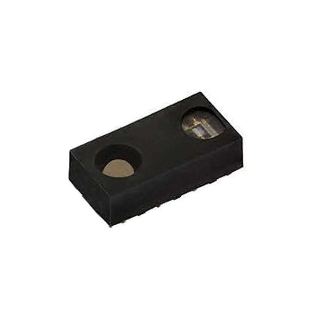
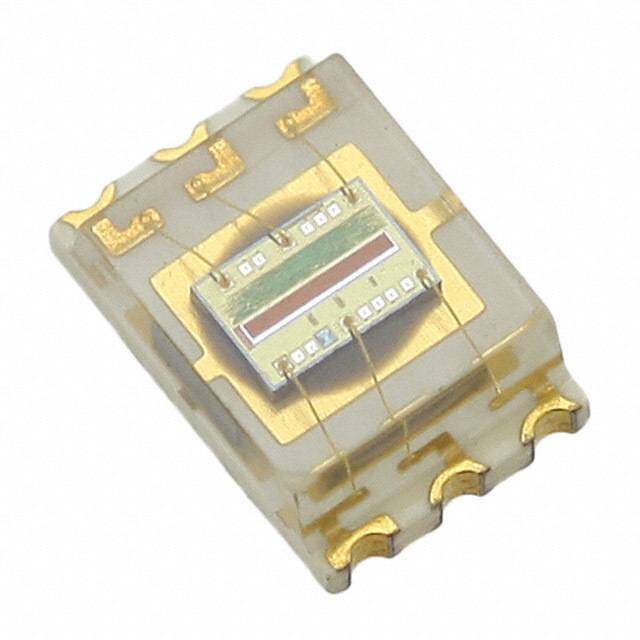
| 描述 | IC LIGHT TO DGTL CONV 6-DFN |
| 产品分类 | |
| 品牌 | AMS-TAOS USA Inc |
| 数据手册 | |
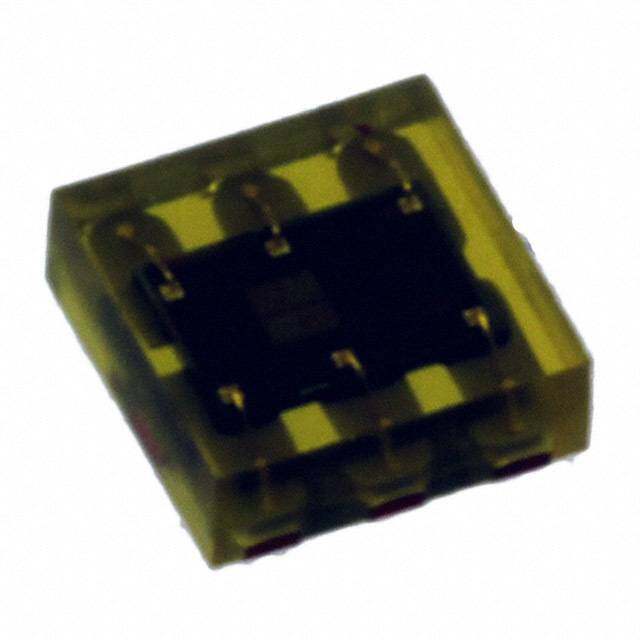
| 产品图片 |
|
| 产品型号 | TSL25715FN |
| rohs | 无铅 / 符合限制有害物质指令(RoHS)规范要求 |
| 产品系列 | - |
| 供应商器件封装 | 6-ODFN (2x2) |
| 其它名称 | TSL25715-FNCT |
| 包装 | 剪切带 (CT) |
| 安装类型 | 表面贴装 |
| 封装/外壳 | 6-WDFN |
| 工作温度 | -30°C ~ 70°C |
| 带接近传感器 | 无 |
| 标准包装 | 1 |
| 波长 | 625nm |
| 电压-电源 | 2.6 V ~ 3.6 V |
| 类型 | 环境 |
| 输出类型 | I²C |


- 商务部:美国ITC正式对集成电路等产品启动337调查
- 曝三星4nm工艺存在良率问题 高通将骁龙8 Gen1或转产台积电
- 太阳诱电将投资9.5亿元在常州建新厂生产MLCC 预计2023年完工
- 英特尔发布欧洲新工厂建设计划 深化IDM 2.0 战略
- 台积电先进制程称霸业界 有大客户加持明年业绩稳了
- 达到5530亿美元!SIA预计今年全球半导体销售额将创下新高
- 英特尔拟将自动驾驶子公司Mobileye上市 估值或超500亿美元
- 三星加码芯片和SET,合并消费电子和移动部门,撤换高东真等 CEO
- 三星电子宣布重大人事变动 还合并消费电子和移动部门
- 海关总署:前11个月进口集成电路产品价值2.52万亿元 增长14.8%


PDF Datasheet 数据手册内容提取
TSL2571 Light-to-Digital Converter General Description The TSL2571 family of devices provides ambient light sensing (ALS) that approximates human eye response to light intensity under a variety of lighting conditions and through a variety of attenuation materials. While useful for general purpose light sensing, the device is particularly useful for display management with the purpose of extending battery life and providing optimum viewing in diverse lighting conditions. Display panel and keyboard backlighting can account for up to 30 to 40 percent of total platform power. The ALS features are ideal for use in notebook PCs, LCD monitors, flat-panel televisions, and cell phones. OrderingInformation and ContentGuide appear at end of datasheet. Key Benefits & Features The benefits and features of TSL2571, Light-to-Digital Converter are listed below: Figure 1: Added Value Of Using TSL2571 Benefits Features • Enables Operation in IR Light Environments • Patented Dual-Diode Architecture • Enables Dark Room to High Lux Sunlight • 1M:1 Dynamic Range Operation • Digital Interface is Less Susceptible to • I2C Digital Interface Noise • Enables Low Standby Power Consumption • 2.5μA Quiescent Current (Sleep Mode) • Reduces Board Space Requirements while • Available in 2mm x 2mm Dual Flat No-Lead (FN) Packages Simplifying Designs • Ambient Light Sensing (ALS) • Approximates Human Eye Response • Programmable Analog Gain • Programmable Integration Time • Programmable Interrupt Function with Upper and Lower Threshold • Resolution Up to 16 Bits • Very High Sensitivity — Operates Well Behind Darkened Glass • Up to 1,000,000:1 Dynamic Range ams Datasheet Page 1 [v1-01] 2018-Mar-27 DocumentFeedback
TSL2571 − General Description • Programmable Wait Timer • Programmable from 2.72 ms to > 8 Seconds • Wait State — 65μA Typical Current • I²C Interface Compatible • Up to 400 kHz (I²C Fast Mode) • Dedicated Interrupt Pin • Small 2 mm x 2 mm ODFN Package • Sleep Mode — 2.5μA Typical Current Applications TSL2571, Light-to-Digital Converter is ideal for: • Display Management • Backlight Control • Portable Device Power Optimization • Cell Phones, PDA, GPS • Notebooks and Monitors • LCD TVs Functional Block Diagram The functional blocks of this device are shown below: Figure 2: TSL2571 Block Diagram GND Interrupt INT Wait Control Upper Limit V CH0 CH0 DD ADC Data SCL e c a ALS Control Lower Limit erf t CH0 n CH1 CH1 C I SDA 2 I ADC Data CH1 Page 2 ams Datasheet DocumentFeedback [v1-01] 2018-Mar-27
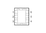
TSL2571 − Pin Assignments Pin Assignments Figure 3: Package FN Dual Flat No-Lead (Top View) V 1 6 SDA DD SCL 2 5 INT GND 3 4 NC Figure 4: Terminal Functions Terminal Type Description Name No V 1 Supply voltage. DD SCL 2 I I²C serial clock input terminal — clock signal for I²C serial data. GND 3 Power supply ground. All voltages are referenced to GND. NC 4 Do not connect. INT 5 O Interrupt — open drain (active low). SDA 6 I/O I²C serial data I/O terminal — serial data I/O for I²C . ams Datasheet Page 3 [v1-01] 2018-Mar-27 DocumentFeedback
TSL2571 − Detailed Description Detailed Description The TSL2571 light-to-digital device includes on-chip photodiodes, integrating amplifiers, ADCs, accumulators, clocks, buffers, comparators, a state machine, and an I²C interface. The device combines one photodiode (CH0), which is responsive to both visible and infrared light, and one photodiode (CH1), which is responsive primarily to infrared light. Two integrating ADCs simultaneously convert the amplified photodiode currents into a digital value providing up to 16 bits of resolution. Upon completion of the conversion cycle, the conversion result is transferred to the data registers. This digital output can be read by a microprocessor through which the illuminance (ambient light level) in lux is derived using an empirical formula to approximate the human eye response. Communication to the device is accomplished through a fast (up to 400 kHz), two-wire I²C serial bus for easy connection to a microcontroller or embedded controller. The digital output of the device is inherently more immune to noise when compared to an analog interface. The device provides a separate pin for level-style interrupts. When interrupts are enabled and a pre-set value is exceeded, the interrupt pin is asserted and remains asserted until cleared by the controlling firmware. The interrupt feature simplifies and improves system efficiency by eliminating the need to poll a sensor for a light intensity value. An interrupt is generated when the value of an ALS conversion exceeds either an upper or lower threshold. In addition, a programmable interrupt persistence feature allows the user to determine how many consecutive exceeded thresholds are necessary to trigger an interrupt. Interrupt thresholds and persistence settings are configured independently. Page 4 ams Datasheet DocumentFeedback [v1-01] 2018-Mar-27
TSL2571 − Absolute Maximum Ratings Absolute Maximum Ratings Stresses beyond those listed under Absolute Maximum Ratings may cause permanent damage to the device. These are stress ratings only, and functional operation of the device at these or any other conditions beyond those indicated under Recommended Operating Conditions is not implied. Exposure to absolute-maximum-rated conditions for extended periods may affect device reliability. Figure 5: Absolute Maximum Ratings Over Operating Free-Air Temperature Range (unless otherwise noted) Symbol Parameter Min Max Units V (1) Supply voltage 3.8 V DD V Digital output voltage range -0.5 3.8 V O I Digital Output current -1 +20 mA O T Storage temperature range -40 85 °C STRG ESD ESD tolerance, human body model ±2000 V HBM Note(s): 1. All voltages are with respect to GND. ams Datasheet Page 5 [v1-01] 2018-Mar-27 DocumentFeedback
TSL2571 − Electrical Characteristics Electrical Characteristics Figure 6: Recommended Operating Conditions Symbol Parameter Min Typ Max Units V Supply voltage 2.6 3 3.6 V DD T Operating free-air temperature -30 70 °C A Figure 7: Operating Characteristics; V = 3V, T = 25°C (unless otherwise noted) DD A Symbol Parameter Test Conditions Min Typ Max Unit Active 175 250 Wait mode 65 I Supply current μA DD Sleep mode — no I²C 2.5 4 activity 3 mA sink current 0 0.4 V INT SDA output low voltage V OL 6 mA sink current 0 0.6 Leakage current, SDA, SCL, I −5 5 μA LEAK INT pins TSL25711, TSL25715 0.7 V DD V SCL SDA input high voltage V IH TSL25713 1.25 TSL25711, TSL25715 0.3 V DD V SCL SDA input low voltage V IL TSL25713 0.54 Page 6 ams Datasheet DocumentFeedback [v1-01] 2018-Mar-27
TSL2571 − Electrical Characteristics Figure 8: ALS Characteristics; V = 3V, T = 25°C, Gain = 16, AEN = 1 (unless otherwise noted)(1) (2) (3) DD A Parameter Test Conditions Channel Min Typ Max Unit E = 0, AGAIN = 120× CH0 0 1 5 Dark ADC count value e counts ATIME = 0xDB (100 ms) CH1 0 1 5 ADC integration time ATIME = 0xFF 2.58 2.72 2.9 ms step size ADC Number of 1 256 steps integration steps ADC counts per step ATIME = 0xFF 0 1024 counts ADC count value ATIME = 0xC0 0 65535 counts λ = 625 nm, E = 171.6 CH0 4000 5000 6000 p e μW/cm2 ATIME = 0xF6 (27 ms) (2) CH1 790 ADC count value counts λ = 850 nm, E = 219.7 CH0 4000 5000 6000 p e μW/cm2 ATIME = 0xF6 (27 ms) (3) CH1 2800 λ = 625 ATIME 0xF6 (27 ms) (2) 10.8 15.8 20.8 ADC count value p % ratio: CH1/CH0 λ = 850 ATIME 0xF6 (27 ms) (3) 41 56 68 p λ = 625 nm, ATIME = 0xF6 CH0 29.1 p (27 ms) (2) CH1 4.6 R Irradiance counts/ e responsivity (μW/ cm2) λ = 850 nm, ATIME = 0xF6 CH0 22.8 p (27 ms) (3) CH1 12.7 8× −10 10 Gain scaling, relative 16× −10 10 % to 1× gain setting 120× −10 10 Note(s): 1. Optical measurements are made using small-angle incident radiation from light-emitting diode optical sources. Visible 625 nm LEDs and infrared 850 nm LEDs are used for final product testing for compatibility with high-volume production. 2. The 625 nm irradiance Ee is supplied by an AlInGaP light-emitting diode with the following typical characteristics: peak wavelength λp = 625 nm and spectral halfwidth Δλ½ = 20 nm. 3. The 850 nm irradiance Ee is supplied by a GaAs light-emitting diode with the following typical characteristics: peak wavelength λp = 850 nm and spectral halfwidth Δλ½ = 42 nm. ams Datasheet Page 7 [v1-01] 2018-Mar-27 DocumentFeedback
TSL2571 − Electrical Characteristics Figure 9: Wait Characteristics; V = 3V, T = 25°C, WEN = 1 (unless otherwise noted) DD A Parameter Test Conditions Channel Min Typ Max Unit Wait step size WTIME = 0xFF 2.58 2.72 2.9 ms Wait number of 1 256 steps integration steps Figure 10: AC Electrical Characteristics; V = 3V, T = 25°C, (unless otherwise noted) DD A Test Symbol Parameter(1) Min Typ Max Unit Conditions f Clock frequency (I²C only) 0 400 kHz (SCL) Bus free time between start and stop t 1.3 μs (BUF) condition Hold time after (repeated) start t condition. After this period, the first 0.6 μs (HDSTA) clock is generated. t Repeated start condition setup time 0.6 μs (SUSTA) t Stop condition setup time 0.6 μs (SUSTO) t Data hold time 0 μs (HDDAT) t Data setup time 100 ns (SUDAT) t SCL clock low period 1.3 μs (LOW) t SCL clock high period 0.6 μs (HIGH) t Clock/data fall time 300 ns F t Clock/data rise time 300 ns R C Input pin capacitance 10 pF i Note(s): 1. Specified by design and characterization; not production tested. Page 8 ams Datasheet DocumentFeedback [v1-01] 2018-Mar-27
TSL2571 − Electrical Characteristics Figure 11: Timing Diagrams - Parameter Measurement Information t(LOW) t(R) t(F) SCL VIH VIL t(HDSTA) t(HIGH) t(SUSTA) t(BUF) t(HDDAT) t(SUDAT) t(SUSTO) SDA VIH VIL P S S P Stop Start Start Stop Condition Condition t(LOWSEXT) SCLACK SCLACK t(LOWMEXT) t(LOWMEXT) t(LOWMEXT) SCL SDA ams Datasheet Page 9 [v1-01] 2018-Mar-27 DocumentFeedback
TSL2571 − Typical Characteristics Typical Characteristics Figure 12: Spectral Responsivity 1 Ch 0 0.8 y vit si n o 0.6 p s e R d e z 0.4 ali m or Ch 1 N 0.2 0 300 400 500 600 700 800 900 1000 1100 λ − Wavelength − nm Figure 13: Normalized I vs.V and Temperature DD DD V and TEMPERATURE DD 110% 108% 75(cid:2)C 106% C (cid:2) 5 2 3 V, 104% 50(cid:2)C 25(cid:2)C @ 102% d e z ali 100% m 0(cid:2)C r o 98% N D D I 96% 94% 92% 2.7 2.8 2.9 3 3.1 3.2 3.3 VDD — V Page 10 ams Datasheet DocumentFeedback [v1-01] 2018-Mar-27
TSL2571 − Typical Characteristics Figure 14: Normalized Responsivity vs. Angular Displacement 1.0 0.8 y vit s si xi pon 0.6 al A s c Re pti d O e z 0.4 ali m r o N 0.2 (cid:3)(cid:2) (cid:4)(cid:2) 0 −90 −60 −30 0 30 60 90 (cid:2) − Angular Displacement − ° ams Datasheet Page 11 [v1-01] 2018-Mar-27 DocumentFeedback
TSL2571 − Principles of Operation Principles of Operation System State Machine The device provides control of ALS and power management functionality through an internal state machine (see Figure15). After a power-on-reset, the device is in the sleep mode. As soon as the PON bit is set, the device will move to the start state. It will then continue through the Wait and ALS states. If these states are enabled, the device will execute each function. If the PON bit is set to 0, the state machine will continue until all conversions are completed and then go into a low power sleep mode. Figure 15: Simplified State Diagram Sleep PON = 1 (r0:b0) PON = 0 (r0:b0) Start ALS Wait Note(s): In this document, the nomenclature uses the bit field name in italic followed by the register number and bit number to allow the user to easily identify the register and bit that controls the function. For example, the power on (PON) is in register 0, bit 0. This is represented as PON (r0:b0). Page 12 ams Datasheet DocumentFeedback [v1-01] 2018-Mar-27
TSL2571 − Principles of Operation Photodiodes Conventional silicon detectors respond strongly to infrared light, which the human eye does not see. This can lead to significant error when the infrared content of the ambient light is high (such as with incandescent lighting) due to the difference between the silicon detector response and the brightness perceived by the human eye. This problem is overcome through the use of two photodiodes. The channel 0 photodiode, referred to as the CH0 channel, is sensitive to both visible and infrared light, while the channel 1 photodiode, referred to as CH1, is sensitive primarily to infrared light. Two integrating ADCs convert the photodiode currents to digital outputs. The ADC digital outputs from the two channels are used in a formula to obtain a value that approximates the human eye response in units of lux. ALS Operation The ALS engine contains ALS gain control (AGAIN) and two integrating analog-to-digital converters (ADC) for the Channel 0 and Channel 1 photodiodes. The ALS integration time (ATIME) impacts both the resolution and the sensitivity of the ALS reading. Integration of both channels occurs simultaneously and upon completion of the conversion cycle, the results are transferred to the data registers (C0DATA and C1DATA). This data is also referred to as channel count. The transfers are double-buffered to ensure data integrity. Figure 16: ALS Operation ATIME(r1) 2.72 ms to 696 ms CH0 CH0 C0DATAH(r0x15), C0DATA(r0x14) ALS Data ALS Control CH0 CH1 CH1 ADC Data C1DATAH(r0x17), C1DATA(r0x16) CH1 AGAIN(r0x0F, b1:0) 1(cid:3), 8(cid:3), 16(cid:3), 120(cid:3) Gain ams Datasheet Page 13 [v1-01] 2018-Mar-27 DocumentFeedback
TSL2571 − Principles of Operation The registers for programming the integration and wait times are a 2’s compliment values. The actual time can be calculated as follows: ATIME = 256 - Integration Time / 2.72 ms Inversely, the time can be calculated from the register value as follows: Integration Time = 2.72 ms × (256 - ATIME) In order to reject 50/60-Hz ripple strongly present in fluorescent lighting, the integration time needs to be programmed in multiples of 10 / 8.3 ms or the half cycle time. Both frequencies can be rejected with a programmed value of 50 ms (ATIME = 0xED) or multiples of 50 ms (i.e. 100, 150, 200, 400, 600). The registers for programming the AGAIN hold a two-bit value representing a gain of 1×, 8×, 16×, or 120×. The gain, in terms of amount of gain, will be represented by the value AGAINx, i.e. AGAINx = 1, 8, 16, or 120. Lux Equation The lux calculation is a function of CH0 channel count (C0DATA), CH1 channel count (C1DATA), ALS gain (AGAINx), and ALS integration time in milliseconds (ATIME_ms). If an aperture, glass/plastic, or a light pipe attenuates the light equally across the spectrum (300 nm to 1100 nm), then a scaling factor referred to as glass attenuation (GA) can be used to compensate for attenuation. For a device in open air with no aperture or glass/plastic above the device, GA = 1. If it is not spectrally flat, then a custom lux equation with new coefficients should be generated. (See ams application note). Counts per Lux (CPL) needs to be calculated only when ATIME or AGAIN is changed, otherwise it remains a constant. The first segment of the equation (Lux1) covers fluorescent and incandescent light. The second segment (Lux2) covers dimmed incandescent light. The final lux is the maximum of Lux1, Lux2, or 0. CPL = (ATIME_ms × AGAINx) / (GA × 53) Lux1 = (C0DATA - 2 × C1DATA) / CPL Lux2 = (0.6 × C0DATA - C1DATA) / CPL Lux = MAX(Lux1, Lux2, 0) Page 14 ams Datasheet DocumentFeedback [v1-01] 2018-Mar-27
TSL2571 − Principles of Operation Interrupts The interrupt feature simplifies and improves system efficiency by eliminating the need to poll the sensor for light intensity values outside of a user-defined range. While the interrupt function is always enabled and it’s status is available in the status register (0x13), the output of the interrupt state can be enabled using the ALS interrupt enable (AIEN) field in the enable register (0x00). Two 16-bit interrupt threshold registers allow the user to set limits below and above a desired light level range. An interrupt can be generated when the ALS CH0 data (C0DATA) falls outside of the desired light level range, as determined by the values in the ALS interrupt low threshold registers (AILTx) and ALS interrupt high threshold registers (AIHTx). It is important to note that the low threshold value must be less than the high threshold value for proper operation. To further control when an interrupt occurs, the device provides a persistence filter. The persistence filter allows the user to specify the number of consecutive out-of-range ALS occurrences before an interrupt is generated. The persistence register (0x0C) allows the user to set the ALS persistence (APERS) value. See the persistence register for details on the persistence filter values. Once the persistence filter generates an interrupt, it will continue until a special function interrupt clear command is received (see Command Register). Figure 17: Programmable Interrupt AIHTH(r07), AIHTL(r06) APERS(r0x0C, b3:0) Upper Limit ALS Persistence CH0 CH0 ADC Data Lower Limit CH0 AILTH(r05), AILTL(r04) ams Datasheet Page 15 [v1-01] 2018-Mar-27 DocumentFeedback
State Diagram Figure18 shows a more detailed flow for the state machine. The device starts in the sleep mode. The PON bit is written to enable the device. A 2.72-ms delay will occur before entering the start state. If the WEN bit is set, the state machine will then cycle through the wait state. If the WLONG bit is set, the wait cycles are extended by 12× over normal operation. When the wait counter terminates, the state machine will step to the ALS state. The AEN should always be set. In this case, a minimum of 1 integration time step should be programmed. The ALS state machine will continue until it reaches the terminal count at which point the data will be latched in the ALS register and the interrupt set, if enabled. Figure 18: Expanded State Diagram 1 to 256 steps Sleep Step: 2.72 ms Time: 2.72 ms − 696 ms PON = 1 PON = 0 120 Hz Minimum − 8 ms 100 Hz Minimum − 10 ms Start ALS ALS Check ALS AEN = 1 Delay Wait Check 2.72 ms WEN = 1 Wait WLONG = 0 WLONG = 1 1 to 256 steps 1 to 256 steps Step: 2.72 ms Step: 32.64 ms Time: 2.72 ms − 696 ms Time: 32.64 ms − 8.35 s Minimum − 2.72 ms Minimum − 32.64 ms Page 16 ams Datasheet DocumentFeedback [v1-01] 2018-Mar-27
TSL2571 − Principles of Operation I²C Protocol Interface and control are accomplished through an I²C serial compatible interface (standard or fast mode) to a set of registers that provide access to device control functions and output data. The devices support the 7-bit I²C addressing protocol. The I²C standard provides for three types of bus transaction: read, write, and a combined protocol (see Figure34). During a write operation, the first byte written is a command byte followed by data. In a combined protocol, the first byte written is the command byte followed by reading a series of bytes. If a read command is issued, the register address from the previous command will be used for data access. Likewise, if the MSB of the command is not set, the device will write a series of bytes at the address stored in the last valid command with a register address. The command byte contains either control information or a 5-bit register address. The control commands can also be used to clear interrupts. The I²C bus protocol was developed by Philips (now NXP). For a complete description of the I²C protocol, please review the NXP I²C design specification at http://www.i2c-bus.org/references/. Figure 19: I²C Protocols 1 7 1 1 8 1 8 1 1 ... S Slave Address W A Command Code A Data Byte A P I2C Write Protocol 1 7 1 1 8 1 8 1 1 ... S Slave Address R A Data A Data A P I2C Read Protocol 1 7 1 1 8 1 1 7 1 1 S Slave Address W A Command Code A S Slave Address R A 8 1 8 1 1 ... Data A Data A P A Acknowledge (0) N Not Acknowledged (1) P Stop Condition R Read (1) S Start Condition S Repeated Start Condition W Write (0) ... Continuation of protocol Master-to-Slave Slave-to-Master ams Datasheet Page 17 [v1-01] 2018-Mar-27 DocumentFeedback
TSL2571 − Register Description Register Description Register Set The device is controlled and monitored by data registers and a command register accessed through the serial interface. These registers provide for a variety of control functions and can be read to determine results of the ADC conversions. The register set is summarized in Figure20. Figure 20: Register Address Address Register Name R/W Register Function Reset Value −− COMMAND W Specifies register address 0x00 0x00 ENABLE R/W Enables states and interrupts 0x00 0x01 ATIME R/W ALS ADC time 0xFF 0x03 WTIME R/W Wait time 0xFF 0x04 AILTL R/W ALS interrupt low threshold low byte 0x00 0x05 AILTH R/W ALS interrupt low threshold high byte 0x00 0x06 AIHTL R/W ALS interrupt high threshold low byte 0x00 0x07 AIHTH R/W ALS interrupt high threshold high byte 0x00 0x0C PERS R/W Interrupt persistence filters 0x00 0x0D CONFIG R/W Configuration 0x00 0x0F CONTROL R/W Control register 0x00 0x12 ID R Device ID ID 0x13 STATUS R Device status 0x00 0x14 C0DATA R CH0 ADC low data register 0x00 0x15 C0DATAH R CH0 ADC high data register 0x00 0x16 C1DATA R CH1 ADC low data register 0x00 0x17 C1DATAH R CH1 ADC high data register 0x00 The mechanics of accessing a specific register depends on the specific protocol used. See the section on I²C protocols on the previous pages. In general, the COMMAND register is written first to specify the specific control/status register for following read/write operations. Page 18 ams Datasheet DocumentFeedback [v1-01] 2018-Mar-27
TSL2571 − Register Description Command Register The command registers specifies the address of the target register for future write and read operations. Figure 21: Command Register 7 6 5 4 3 2 1 0 COMMAND COMMAND TYPE ADD − − Field Bits Description COMMAND 7 Select Command Register. Must write as 1 when addressing COMMAND register. Selects type of transaction to follow in subsequent data transfers. FIELD VALUE DESCRIPTION 00 Repeated byte protocol transaction 01 Auto-increment protocol transaction TYPE 6:5 10 Reserved — Do not use 11 Special function — See description below Transaction type 00 will repeatedly read the same register with each data access. Transaction type 01 will provide an auto-increment function to read successive register bytes. Address register/special function field. Depending on the transaction type, see above, this field either specifies a special function command or selects the specific control-status-register for following write and read transactions. The field values listed below apply only to special function commands: FIELD VALUE DESCRIPTION ADD 4:0 00000 Normal — no action 00110 ALS interrupt clear other Reserved — do not write ALS interrupt clear — clears any pending ALS interrupt. This special function is self clearing. ams Datasheet Page 19 [v1-01] 2018-Mar-27 DocumentFeedback
TSL2571 − Register Description Enable Register (0x00) The ENABLE register is used to power the device ON/OFF, enable functions, and interrupts. Figure 22: Enable Register 7 6 5 4 3 2 1 0 Address ENABLE Reserved AIEN WEN Reserved AEN PON 0x00 Field Bits Description Reserved 7:5 Reserved. Write as 0. AIEN 4 ALS interrupt mask. When asserted, permits ALS interrupts to be generated. Wait enable. This bit activates the wait feature. Writing a 1 activates the wait timer. WEN 3 Writing a 0 disables the wait timer. Reserved 2 Reserved. Write as 0. AEN 1 ALS Enable. Writing a 1 activates the ALS. Writing a 0 disables the ALS. Power ON. This bit activates the internal oscillator to permit the timers and ADC PON (1) 0 channels to operate. Writing a 1 activates the oscillator. Writing a 0 disables the oscillator. Note(s): 1. A minimum interval of 2.72 ms must pass after PON is asserted before ALS can be initiated. This required time is enforced by the hardware in cases where the firmware does not provide it. Page 20 ams Datasheet DocumentFeedback [v1-01] 2018-Mar-27
TSL2571 − Register Description ALS Timing Register (0x01) The ALS timing register controls the internal integration time of the ALS ADCs in 2.72-ms increments. Figure 23: ALS Timing Register Field Bits Description VALUE INTEG_CYCLES TIME MAX COUNT 0xFF 1 2.72 ms 1024 0xF6 10 27.2 ms 10240 ATIME 7:0 0xDB 37 101 ms 37888 0xC0 64 174 ms 65535 0x00 256 696 ms 65535 Wait Time Register (0x03) Wait time is set 2.72 ms increments unless the WLONG bit is asserted in which case the wait times are 12× longer. WTIME is programmed as a 2’s complement number. Figure 24: Wait Time Register Field Bits Description REGISTER WAIT TIME TIME (WLONG = 0) TIME (WLONG = 1) VALUE 0xFF 1 2.72 ms 0.032 s WTIME 7:0 0xB6 74 201 ms 2.4 s 0x00 256 696 ms 8.3 s Note(s): 1. The Wait Time Register should be configured before AEN is asserted. ams Datasheet Page 21 [v1-01] 2018-Mar-27 DocumentFeedback
TSL2571 − Register Description ALS Interrupt Threshold Registers (0x04 - 0x07) The ALS interrupt threshold registers provides the values to be used as the high and low trigger points for the comparison function for interrupt generation. If C0DATA crosses below the low threshold specified, or above the higher threshold, an interrupt is asserted on the interrupt pin. Figure 25: ALS Interrupt Threshold Registers Register Address Bits Description AILTL 0x04 7:0 ALS low threshold lower byte AILTH 0x05 7:0 ALS low threshold upper byte AIHTL 0x06 7:0 ALS high threshold lower byte AIHTH 0x07 7:0 ALS high threshold upper byte Page 22 ams Datasheet DocumentFeedback [v1-01] 2018-Mar-27
TSL2571 − Register Description Persistence Register (0x0C) The persistence register controls the filtering interrupt capabilities of the device. Configurable filtering is provided to allow interrupts to be generated after each ADC integration cycle or if the ADC integration has produced a result that is outside of the values specified by threshold register for some specified amount of time. ALS interrupts are generated using C0DATA. Figure 26: Persistence Register 7 6 5 4 3 2 1 0 Address PERS Reserved APERS 0x0C Field Bits Description Reserved 7:4 Reserved Interrupt persistence. Controls rate of interrupt to the host processor. FIELD VALUE MEANING INTERRUPT PERSISTENCE FUNCTION 0000 Every Every ALS cycle generates an interrupt 0001 1 1 value outside of threshold range 0010 2 2 consecutive values out of range 0011 3 3 consecutive values out of range 0100 5 5 consecutive values out of range 0101 10 10 consecutive values out of range 0110 15 15 consecutive values out of range APERS 3:0 0111 20 20 consecutive values out of range 1000 25 25 consecutive values out of range 1001 30 30 consecutive values out of range 1010 35 35 consecutive values out of range 1011 40 40 consecutive values out of range 1100 45 45 consecutive values out of range 1101 50 50 consecutive values out of range 1110 55 55 consecutive values out of range 1111 60 60 consecutive values out of range ams Datasheet Page 23 [v1-01] 2018-Mar-27 DocumentFeedback
TSL2571 − Register Description Configuration Register (0x0D) The configuration register sets the wait long time. Figure 27: Configuration Register 7 6 5 4 3 2 1 0 Address CONFIG Reserved WLONG Reserved 0x0D Field Bits Description Reserved 7:2 Reserved. Write as 0. Wait Long. When asserted, the wait cycles are increased by a factor 12× from WLONG 1 that programmed in the WTIME register. Reserved 0 Reserved. Write as 0. Control Register (0x0F) The Control register provides eight bits of miscellaneous control to the analog block. These bits typically control functions such as gain settings and/or diode selection. Figure 28: Control Register 7 6 5 4 3 2 1 0 Address CONTROL Reserved AGAIN 0x0F Field Bits Description Reserved 7:2 Reserved. Write bits as 0 ALS Gain Control. FIELD VALUE ALS GAIN VALUE 00 1× gain AGAIN 1:0 01 8× gain 10 16× gain 11 120× gain Page 24 ams Datasheet DocumentFeedback [v1-01] 2018-Mar-27
TSL2571 − Register Description ID Register (0x12) The ID Register provides the value for the part number. The ID register is a read-only register. Figure 29: ID Register 7 6 5 4 3 2 1 0 Address ID ID 0x12 Field Bits Description 0x04 = TSL25711 and TSL25715 ID 7:0 Part number identification 0x0D = TSL25713 Status Register (0x13) The Status Register provides the internal status of the device. This register is read only. Figure 30: Status Register 7 6 5 4 3 2 1 0 Address STATUS Reserved AINT Reserved AVALID 0x13 Field Bit Description Reserved 7:5 Reserved. Write as 0. AINT 4 ALS Interrupt. Indicates that the device is asserting an ALS interrupt. Reserved 3:1 Reserved. ALS Valid. Indicates that the ALS CH0 / CH1 channels have completed AVALID 0 an integration cycle. ams Datasheet Page 25 [v1-01] 2018-Mar-27 DocumentFeedback
TSL2571 − Register Description ADC Channel Data Registers (0x14 - 0x17) ALS data is stored as two 16-bit values. To ensure the data is read correctly, a two-byte read I²C transaction should be used with auto increment protocol bits set in the command register. With this operation, when the lower byte register is read, the upper eight bits are stored in a shadow register, which is read by a subsequent read to the upper byte. The upper register will read the correct value even if additional ADC integration cycles end between the reading of the lower and upper registers. Figure 31: ADC Channel Data Registers Register Address Bits Description C0DATA 0x14 7:0 ALS CH0 data low byte C0DATAH 0x15 7:0 ALS CH0 data high byte C1DATA 0x16 7:0 ALS CH1 data low byte C1DATAH 0x17 7:0 ALS CH1 data high byte Page 26 ams Datasheet DocumentFeedback [v1-01] 2018-Mar-27
TSL2571 − Application Information Hardware Application Information Hardware Typical Hardware Application A typical hardware application circuit is shown in Figure32. A 1-μF low-ESR decoupling capacitor should be placed as close as possible to the VDD pin. Figure 32: Typical Application Hardware Circuit V V DD BUS V DD R R R P P PI 1 (cid:5)F TSL2571 INT SCL GND SDA V in Figure32 refers to the I²C bus voltage, which is either BUS V or 1.8 V. Be sure to apply the specified I²C bus voltage shown DD in the Available Options table for the specific device being used. The I²C signals and the Interrupt are open-drain outputs and require pull-up resistors. The pull-up resistor (R ) value is a P function of the I²C bus speed, the I²C bus voltage, and the capacitive load. The ams EVM running at 400 kbps, uses 1.5-kΩ resistors. A 10-kΩ pull-up resistor (RPI) can be used for the interrupt line. ams Datasheet Page 27 [v1-01] 2018-Mar-27 DocumentFeedback
TSL2571 − Application Information Hardware PCB Pad Layout Suggested PCB pad layout guidelines for the Dual Flat No-Lead (FN) surface mount package are shown in Figure33. Note(s): Pads can be extended further if hand soldering is needed. Figure 33: Suggested FN Package PCB Layout 2500 1000 1000 400 650 1700 650 400 Note(s): 1. All linear dimensions are in micrometers. 2. This drawing is subject to change without notice. Page 28 ams Datasheet DocumentFeedback [v1-01] 2018-Mar-27
TSL2571 − Mechanical Data Mechanical Data Figure 34: Package FN — Dual Flat No-Lead Packaging Configuration PACKAGE FN Dual Flat No-Lead TOP VIEW 466 (cid:4) 10 PIN OUT TOP VIEW PIN 1 V 1 6 SDA DD 466 (cid:4) 10 2000 (cid:4) 100 SCL 2 5 INT GND 3 4 NC 2000 Photodiode Array Area (cid:4) 100 END VIEW SIDE VIEW 295 Nominal 650 (cid:4) 50 203 (cid:4) 8 650 BOTTOM VIEW 300 (cid:4) 50 CLof Photodiode Array Area CLof Solder Contacts (Note (cid:21)) 20 Nominal 140 Nominal CLof Solder Contacts CL of Photodiode Array Area (Note (cid:21)) PIN 1 Pb RoHS Green 750 (cid:4) 150 Lead Free Note(s): 1. All linear dimensions are in micrometers. Dimension tolerance is ±20μm unless otherwise noted. 2. The die is centered within the package within a tolerance of ± 3 mils. 3. Package top surface is molded with an electrically nonconductive clear plastic compound having an index of refraction of 1.55. 4. Contact finish is copper alloy A194 with pre-plated NiPdAu lead finish. 5. This package contains no lead (Pb). 6. This drawing is subject to change without notice. ams Datasheet Page 29 [v1-01] 2018-Mar-27 DocumentFeedback
TSL2571 − Mechanical Data Figure 35: Package FN Carrier Tape TOP VIEW 2.00 (cid:4) 0.05 1.75 4.00 4.00 (cid:5) 1.50 B + 0.30 8.00 − 0.10 3.50 (cid:4) 0.05 (cid:5) 1.00 (cid:4) 0.25 A A B DETAIL A DETAIL B 5(cid:2) Max 5(cid:2) Max 0.254 2.18 (cid:4) 0.05 (cid:4) 0.02 0.83 (cid:4) 0.05 2.18 (cid:4) 0.05 Ao Ko Bo Note(s): 1. All linear dimensions are in millimeters. Dimension tolerance is ±0.10 mm unless otherwise noted. 2. The dimensions on this drawing are for illustrative purposes only. Dimensions of an actual carrier may vary slightly. 3. Symbols on drawing A , B , and K are defined in ANSI EIA Standard 481-B 2001. o o o 4. Each reel is 178 millimeters in diameter and contains 3500 parts. 5. ams packaging tape and reel conform to the requirements of EIA Standard 481-B. 6. In accordance with EIA standard, device pin 1 is located next to the sprocket holes in the tape. 7. This drawing is subject to change without notice. Page 30 ams Datasheet DocumentFeedback [v1-01] 2018-Mar-27
TSL2571 − Manufacturing Information Manufacturing Information The FN package has been tested and has demonstrated an ability to be reflow soldered to a PCB substrate. The solder reflow profile describes the expected maximum heat exposure of components during the solder reflow process of product on a PCB. Temperature is measured on top of component. The components should be limited to a maximum of three passes through this solder reflow profile. Figure 36: Soldier Reflow Profile Parameter Reference Device Average temperature gradient in preheating 2.5°C/s Soak time t 2 to 3 minutes soak Time above 217°C (T ) t Max 60 s 1 1 Time above 230°C (T ) t Max 50 s 2 2 Time above T −10°C (T ) t Max 10 s peak 3 3 Peak temperature in reflow T 260°C peak Temperature gradient in cooling Max −5°C/s Figure 37: Solder Reflow Profile Graph Not to scale — for reference o T peak T 3 T 2 T 1 C) (cid:2) e ( r u at r e p m e T Time (s) t 3 t 2 tsoak t1 Note(s): 1. Not to scale - for reference only. ams Datasheet Page 31 [v1-01] 2018-Mar-27 DocumentFeedback
TSL2571 − Manufacturing Information Moisture Sensitivity Optical characteristics of the device can be adversely affected during the soldering process by the release and vaporization of moisture that has been previously absorbed into the package. To ensure the package contains the smallest amount of absorbed moisture possible, each device is dry-baked prior to being packed for shipping. Devices are packed in a sealed aluminized envelope called a moisture barrier bag with silica gel to protect them from ambient moisture during shipping, handling, and storage before use. The FN package has been assigned a moisture sensitivity level of MSL 3 and the devices should be stored under the following conditions: • Temperature Range: 5°C to 50°C • Relative Humidity: 60% maximum • Total Time: 12 months from the date code on the aluminized envelope—if unopened • Opened Time: 168 hours or fewer Rebaking will be required if the devices have been stored unopened for more than 12 months or if the aluminized envelope has been open for more than 168 hours. If rebaking is required, it should be done at 50°C for 12 hours. Page 32 ams Datasheet DocumentFeedback [v1-01] 2018-Mar-27
TSL2571 − Ordering & Contact Information Ordering & Contact Information Figure 38: Ordering Information Package - Ordering Code Device Address Interface Description Leads TSL25711FN TSL25711 0x39 FN−6 I²C Vbus = V Interface DD TSL25713FN TSL25713 0x39 FN−6 I²C Vbus = 1.8 V Interface TSL25715FN TSL25715 0x29 FN−6 I²C Vbus = V Interface DD Buy our products or get free samples online at: www.ams.com/ICdirect Technical Support is available at: www.ams.com/Technical-Support Provide feedback about this document at: www.ams.com/Document-Feedback For further information and requests, e-mail us at: ams_sales@ams.com For sales offices, distributors and representatives, please visit: www.ams.com/contact Headquarters ams AG Tobelbader Strasse 30 8141 Premstaetten Austria, Europe Tel: +43 (0) 3136 500 0 Website: www.ams.com ams Datasheet Page 33 [v1-01] 2018-Mar-27 DocumentFeedback
TSL2571 − RoHS Compliant & ams Green Statement RoHS Compliant & ams Green RoHS: The term RoHS compliant means that ams AG products fully comply with current RoHS directives. Our semiconductor Statement products do not contain any chemicals for all 6 substance categories, including the requirement that lead not exceed 0.1% by weight in homogeneous materials. Where designed to be soldered at high temperatures, RoHS compliant products are suitable for use in specified lead-free processes. ams Green (RoHS compliant and no Sb/Br): ams Green defines that in addition to RoHS compliance, our products are free of Bromine (Br) and Antimony (Sb) based flame retardants (Br or Sb do not exceed 0.1% by weight in homogeneous material). Important Information: The information provided in this statement represents ams AG knowledge and belief as of the date that it is provided. ams AG bases its knowledge and belief on information provided by third parties, and makes no representation or warranty as to the accuracy of such information. Efforts are underway to better integrate information from third parties. ams AG has taken and continues to take reasonable steps to provide representative and accurate information but may not have conducted destructive testing or chemical analysis on incoming materials and chemicals. ams AG and ams AG suppliers consider certain information to be proprietary, and thus CAS numbers and other limited information may not be available for release. Page 34 ams Datasheet DocumentFeedback [v1-01] 2018-Mar-27
TSL2571 − Copyrights & Disclaimer Copyrights & Disclaimer Copyright ams AG, Tobelbader Strasse 30, 8141 Premstaetten, Austria-Europe. Trademarks Registered. All rights reserved. The material herein may not be reproduced, adapted, merged, translated, stored, or used without the prior written consent of the copyright owner. Devices sold by ams AG are covered by the warranty and patent indemnification provisions appearing in its General Terms of Trade. ams AG makes no warranty, express, statutory, implied, or by description regarding the information set forth herein. ams AG reserves the right to change specifications and prices at any time and without notice. Therefore, prior to designing this product into a system, it is necessary to check with ams AG for current information. This product is intended for use in commercial applications. Applications requiring extended temperature range, unusual environmental requirements, or high reliability applications, such as military, medical life-support or life-sustaining equipment are specifically not recommended without additional processing by ams AG for each application. This product is provided by ams AG “AS IS” and any express or implied warranties, including, but not limited to the implied warranties of merchantability and fitness for a particular purpose are disclaimed. ams AG shall not be liable to recipient or any third party for any damages, including but not limited to personal injury, property damage, loss of profits, loss of use, interruption of business or indirect, special, incidental or consequential damages, of any kind, in connection with or arising out of the furnishing, performance or use of the technical data herein. No obligation or liability to recipient or any third party shall arise or flow out of ams AG rendering of technical or other services. ams Datasheet Page 35 [v1-01] 2018-Mar-27 DocumentFeedback
TSL2571 − Document Status Document Status Document Status Product Status Definition Information in this datasheet is based on product ideas in the planning phase of development. All specifications are Product Preview Pre-Development design goals without any warranty and are subject to change without notice Information in this datasheet is based on products in the design, validation or qualification phase of development. Preliminary Datasheet Pre-Production The performance and parameters shown in this document are preliminary without any warranty and are subject to change without notice Information in this datasheet is based on products in ramp-up to full production or full production which Datasheet Production conform to specifications in accordance with the terms of ams AG standard warranty as given in the General Terms of Trade Information in this datasheet is based on products which conform to specifications in accordance with the terms of Datasheet (discontinued) Discontinued ams AG standard warranty as given in the General Terms of Trade, but these products have been superseded and should not be used for new designs Page 36 ams Datasheet DocumentFeedback [v1-01] 2018-Mar-27
TSL2571 − Revision Information Revision Information Changes from 1-00 (2016-May-26) to current revision 1-01 (2018-Mar-27) Page Updated Figure 7 6 Updated Figure 29 25 Updated Figure 38 33 Note(s): 1. Page and figure numbers for the previous version may differ from page and figure numbers in the current revision. 2. Correction of typographical errors is not explicitly mentioned. ams Datasheet Page 37 [v1-01] 2018-Mar-27 DocumentFeedback
TSL2571 − Content Guide Content Guide 1 General Description 1 Key Benefits & Features 2 Applications 2 Functional Block Diagram 3 Pin Assignments 4 Detailed Description 5 Absolute Maximum Ratings 6 Electrical Characteristics 10 Typical Characteristics 12 Principles of Operation 12 System State Machine 13 Photodiodes 13 ALS Operation 14 Lux Equation 15 Interrupts 16 State Diagram 17 I²C Protocol 18 Register Description 18 Register Set 19 Command Register 20 Enable Register (0x00) 21 ALS Timing Register (0x01) 21 Wait Time Register (0x03) 22 ALS Interrupt Threshold Registers (0x04 - 0x07) 23 Persistence Register (0x0C) 24 Configuration Register (0x0D) 24 Control Register (0x0F) 25 ID Register (0x12) 25 Status Register (0x13) 26 ADC Channel Data Registers (0x14 - 0x17) 27 Application Information Hardware 27 Typical Hardware Application 28 PCB Pad Layout 29 Mechanical Data 31 Manufacturing Information 32 Moisture Sensitivity 33 Ordering & Contact Information 34 RoHS Compliant & ams Green Statement 35 Copyrights & Disclaimer 36 Document Status 37 Revision Information Page 38 ams Datasheet DocumentFeedback [v1-01] 2018-Mar-27
Mouser Electronics Authorized Distributor Click to View Pricing, Inventory, Delivery & Lifecycle Information: a ms: TSL25715FN