ICGOO在线商城 > 集成电路(IC) > 线性 - 放大器 - 仪表,运算放大器,缓冲器放大器 > TSC1021AIPT
 Datasheet下载
- 型号: TSC1021AIPT
- 制造商: STMicroelectronics
- 库位|库存: xxxx|xxxx
- 要求:
| 数量阶梯 | 香港交货 | 国内含税 |
| +xxxx | $xxxx | ¥xxxx |
查看当月历史价格
查看今年历史价格
TSC1021AIPT产品简介:
ICGOO电子元器件商城为您提供TSC1021AIPT由STMicroelectronics设计生产,在icgoo商城现货销售,并且可以通过原厂、代理商等渠道进行代购。 TSC1021AIPT价格参考¥3.92-¥5.43。STMicroelectronicsTSC1021AIPT封装/规格:线性 - 放大器 - 仪表,运算放大器,缓冲器放大器, 电流检测 放大器 1 电路 8-TSSOP。您可以下载TSC1021AIPT参考资料、Datasheet数据手册功能说明书,资料中有TSC1021AIPT 详细功能的应用电路图电压和使用方法及教程。
STMicroelectronics的TSC1021AIPT是一款专为高精度、低功耗应用设计的仪表放大器。其主要应用场景包括以下几个方面:

 1. 医疗设备
   - 心电图(ECG)和脑电图(EEG)设备:TSC1021AIPT具有高共模抑制比(CMRR),能够有效抑制噪声信号,提取微弱的生物电信号。
   - 血压监测仪:用于放大压力传感器输出的小信号,确保测量结果的精确性。
   - 血糖仪和其他便携式诊断设备:其低功耗特性非常适合电池供电的医疗设备。

 2. 工业自动化
   - 传感器信号调理:适用于温度、压力、位移等传感器信号的放大和处理,确保数据采集的高精度。
   - 数据采集系统(DAQ):在多通道数据采集系统中,TSC1021AIPT可提供稳定的增益和低失真性能。
   - 过程控制:用于工业现场的信号放大与传输,支持高可靠性运行。

 3. 消费电子
   - 音频设备:用于麦克风前置放大器,提升音频信号的质量。
   - 智能家居设备:例如环境监测设备中的温湿度传感器信号处理,提供高精度和低功耗的支持。

 4. 汽车电子
   - 胎压监测系统(TPMS):放大压力传感器信号,确保轮胎压力的精准测量。
   - 车载传感器:如加速度计、陀螺仪等信号的放大和处理,满足汽车级应用的严格要求。

 5. 测试与测量
   - 示波器和信号发生器:用于小信号的放大和稳定输出,保证测量设备的精度。
   - 实验室仪器:如pH计、电导率仪等需要高精度信号放大的场合。

 特性总结
- 高共模抑制比(CMRR):有效抑制干扰信号,适合复杂电磁环境。
- 低功耗:延长电池寿命,适合便携式设备。
- 高精度增益设置:通过外部电阻灵活调整增益,满足不同应用场景需求。
- 宽工作温度范围:适应工业和汽车级应用的严苛环境。

总之,TSC1021AIPT凭借其高性能和灵活性,广泛应用于对信号精度和稳定性要求较高的领域。
| 参数 | 数值 |
| -3db带宽 | 800kHz |
| 产品目录 | 集成电路 (IC)半导体 |
| 描述 | IC OPAMP CURR SENS 800KHZ 8TSSOP电流灵敏放大器 High-side current sense amplifier |
| 产品分类 | Linear - Amplifiers - Instrumentation, OP Amps, Buffer Amps集成电路 - IC |
| 品牌 | STMicroelectronics |
| 产品手册 | |
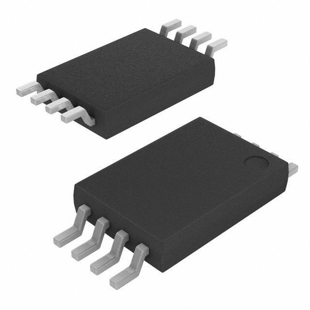
| 产品图片 |
|
| rohs | 符合RoHS无铅 / 符合限制有害物质指令(RoHS)规范要求 |
| 产品系列 | 放大器 IC,电流灵敏放大器,STMicroelectronics TSC1021AIPT- |
| 数据手册 | |
| 产品型号 | TSC1021AIPT |
| 产品种类 | 电流灵敏放大器 |
| 供应商器件封装 | 8-TSSOP |
| 其它名称 | 497-11146-1 |
| 其它有关文件 | http://www.st.com/web/catalog/sense_power/FM123/SC1264/PF250932?referrer=70071840 |
| 准确性 | 1.5 % |
| 包装 | 剪切带 (CT) |
| 压摆率 | 0.45 V/µs |
| 商标 | STMicroelectronics |
| 增益带宽积 | - |
| 安装类型 | 表面贴装 |
| 安装风格 | SMD/SMT |
| 封装 | Reel |
| 封装/外壳 | 8-TSSOP(0.173",4.40mm 宽) |
| 封装/箱体 | TSSOP-8 |
| 工作温度 | -40°C ~ 125°C |
| 工厂包装数量 | 4000 |
| 放大器类型 | 电流检测 |
| 最大工作温度 | + 125 C |
| 最小工作温度 | - 40 C |
| 标准包装 | 1 |
| 电压-电源,单/双 (±) | 3.5 V ~ 5.5 V |
| 电压-输入失调 | 1.5mV |
| 电流-电源 | 300µA |
| 电流-输入偏置 | 7µA |
| 电流-输出/通道 | - |
| 电源电压-最大 | 5.5 V |
| 电源电压-最小 | 3.5 V |
| 电路数 | 1 |
| 系列 | TSC1021 |
| 输入电压 | 3.5 V to 5.5 V |
| 输入补偿电压 | 1.5 mV |
| 输出类型 | - |
| 通道数量 | 1 Channel |


- 商务部:美国ITC正式对集成电路等产品启动337调查
- 曝三星4nm工艺存在良率问题 高通将骁龙8 Gen1或转产台积电
- 太阳诱电将投资9.5亿元在常州建新厂生产MLCC 预计2023年完工
- 英特尔发布欧洲新工厂建设计划 深化IDM 2.0 战略
- 台积电先进制程称霸业界 有大客户加持明年业绩稳了
- 达到5530亿美元!SIA预计今年全球半导体销售额将创下新高
- 英特尔拟将自动驾驶子公司Mobileye上市 估值或超500亿美元
- 三星加码芯片和SET,合并消费电子和移动部门,撤换高东真等 CEO
- 三星电子宣布重大人事变动 还合并消费电子和移动部门
- 海关总署:前11个月进口集成电路产品价值2.52万亿元 增长14.8%


PDF Datasheet 数据手册内容提取
TSC1021 High-side current sense amplifier Datasheet - production data Related products See TSC103 for higher common-mode operating range (2.9 V to 70 V) Applications Automotive current monitoring Notebook computers Server power supplies Telecom equipment Industrial SMPS Current sharing LED current measurement Features Description Wide common-mode operating range The TSC1021 measures a small differential independent of supply: 2.8 V to 30 V voltage on a high-side shunt resistor and Wide common-mode survival range: -32 V to translates it into a ground-referenced output 60 V (reversed battery and load-dump voltage. conditions) Maximum input offset voltage: The TSC1021 has been specifically designed for automotive conditions: load-dump protection up ±1.5 mV for T = 25 °C amb to 60 V, reverse-battery protection up to -32 V, ±2.3 mV for -40 °C < T < 125 °C amb ESD protection up to 4 kV and internal filtering for Maximum total output voltage error: EMI performance. ±1.5 % for T = 25 °C amb ±2.5 % for -40 °C < T < 125 °C Input common-mode and power supply voltages amb Maximum variation over temperature: are independent: the common-mode voltage can dV /dT = 8 µV/°C range from 2.8 to 30 V in operating conditions os dV /dT = 100 ppm/°C and up to 60 V in absolute maximum ratings out while the TSC1021 can be supplied by a 5 V Low current consumption: I max = 300 µA CC independent supply line. -40 °C to 125 °C operating temperature range The TSC1021 is housed in a tiny TSSOP8 Internally fixed gain: 20 V/V, 50 V/V package and integrates a buffer that provides low EMI filtering impedance output to ease interfacing and avoid accuracy losses. The overall device current consumption is lower than 300 µA. November 2015 DocID017857 Rev 4 1/17 This is information on a product in full production. www.st.com
Contents TSC1021 Contents 1 Application diagram ........................................................................ 3 2 Pin configuration ............................................................................. 4 3 Absolute maximum ratings and operating conditions ................. 5 4 Electrical characteristics ................................................................ 6 5 Electrical characteristics curves: current sense amplifier ........... 8 6 Parameter definitions .................................................................... 11 6.1 Common mode rejection ratio (CMR) .............................................. 11 6.2 Supply voltage rejection ratio (SVR) ............................................... 11 6.3 Gain (Av) and input offset voltage (Vos) ......................................... 11 6.4 Output voltage drift versus temperature .......................................... 11 6.5 Output voltage accuracy ................................................................. 12 7 Package information ..................................................................... 13 7.1 TSSOP8 package information ......................................................... 14 8 Ordering information ..................................................................... 15 9 Revision history ............................................................................ 16 2/17 DocID017857 Rev 4
TSC1021 Application diagram 1 Application diagram The TSC1021 high-side current-sense amplifier features a 2.8 V to 30 V input common- mode range that is independent of the supply voltage. The main advantage of this feature is that it allows high-side current sensing at voltages much greater than the supply voltage (V ). CC Figure 1: Application schematic: high-line current sensing DocID017857 Rev 4 3/17
Pin configuration TSC1021 2 Pin configuration Figure 2: Pin connections (top view) Table 1: "Pin description" describes the function of each pin. Their position is shown in the illustration on the cover page and in Figure 2: "Pin connections (top view)" above. Table 1: Pin description Pin Symbol Type Function number Connection for the external sense resistor. The 1 V Analog input m measured current exits the shunt on the V side. m 3 Gnd Power supply Ground line 4 Out Analog output Buffered output of the current sensing amplifier 6 V Power supply Positive power supply line CC Connection for the external sense resistor. The 8 V Analog input p measured current enters the shunt on the V side. p 4/17 DocID017857 Rev 4
TSC1021 Absolute maximum ratings and operating conditions 3 Absolute maximum ratings and operating conditions Table 2: Absolute maximum ratings Symbol Parameter Value Unit V Input pins differential voltage (V -V ) ±20 id p m V Current sensing input pin voltages (V and V ) (1) -32 to 60 V i p m V Voltage for Vcc, Out pins (1) -0.3 to 7 1 T Storage temperature -65 to 150 stg °C T Maximum junction temperature 150 j R TSSOP8 thermal resistance junction to ambient 120 °C/Ω thja HBM: human body model for V and V pins (2) 4 p m kV HBM: human body model for all other pins (2) 2 ESD MM: machine model (3) 250 V CDM: charged device model (4) 1.5 kV Notes: (1)Voltage values are measured with respect to the GND pin. (2)Human body model: a 100 pF capacitor is charged to the specified voltage, then discharged through a 1.5 kΩ resistor between two pins of the device. This is done for all couples of connected pin combinations while the other pins are floating. (3)Machine model: a 200 pF capacitor is charged to the specified voltage, then discharged directly between two pins of the device with no external series resistor (internal resistor < 5 Ω). This is done for all couples of connected pin combinations while the other pins are floating. (4)Charged device model: all pins and package are charged together to the specified voltage and then discharged directly to ground. Table 3: Operating conditions Symbol Parameter Value Unit V DC supply voltage from T to T 3.5 to 5.5 V CC min max T Operational temperature range (T to T ) -40 to 125 °C oper min max V Common-mode voltage range (V and V pin voltage) 2.8 to 30 V icm m p DocID017857 Rev 4 5/17
Electrical characteristics TSC1021 4 Electrical characteristics The electrical characteristics given in the following tables are measured under the following test conditions unless otherwise specified: T = 25 °C, V = 5 V, V = V -V = 50 mV, amb CC sense p m V = 12 V, no load on Out, all gain configurations. m Table 4: Supply Symbol Parameter Test conditions Min. Typ. Max. Unit I Total supply current V = 0 V, -40 °C < T < 125 °C 300 CC sense amb — — µA I Total supply current V = 50 mV, -40 °C < T < 125 °C 450 CC1 sense amb Table 5: Electrical performances Symbol Parameter Test conditions Min. Typ. Max. Unit DC common-mode rejection, variation of V 2.8 V < V < 30 V, DC CMR out m 90 105 versus Vm referred to -40 °C < Tamb < 125 °C input (1) AC common mode rejection, variation of V out 2.8 V < V < 30 V, dB AC CMR versus V referred to input m 75 m DC to 1 kHz sine wave (peak-to-peak voltage variation) Supply voltage rejection, 3.5 V < V < 5.5 V, SVR variation of V versus CC 80 95 V (1) out -40 °C< Tamb < 125°C CC 2.8 V < V < 30 V, T = 25 °C ±1.5 m amb Vos Input offset voltage (1) 2.8 V < Vm < 30 V, ±2.3 mV -40 °C < Tamb < 125 °C dV /dT Input offset drift vs. T -40 °C< T < 125 °C 8 µV/°C os amb dV /dT Output voltage drift vs. T -40 °C< T < 125 °C 100 ppm/°C out amb I Input leakage current V = 0 V, -40 °C < T < 125 °C 1 lk CC amb µA I Input bias current V = 0 V, -40 °C < T < 125 °C 7 ib sense amb Gain, (variation of V TSC1021A 20 Av out V/V versus Vsense) TSC1021B 50 V = 50 mV, T = 25 °C ±1.5 sense amb V = 50 mV, T < T < T ±2.5 sense min amb max V = 100 mV, T = 25 °C ±1.5 sense amb Total output voltage Vsense = 100 mV, Tmin < Tamb < Tmax ±2.5 ΔV % out accuracy (2) V = 20 mV, T = 25 °C ±7 sense amb V = 20 mV, T < T < T ±9 sense min amb max V = 10 mV, T = 25 °C ±12 sense amb V = 10 mV, T < T < T ±15 sense min amb max Output stage load -5 mA < I <5 mA, ΔV /ΔI out ±0.4 ±2 mV/mA out out regulation Iout sink or source current 6/17 DocID017857 Rev 4
TSC1021 Electrical characteristics Symbol Parameter Test conditions Min. Typ. Max. Unit V = 1 V, I = 1 mA, sense out 90 135 Out high level saturation Tamb = 25 °C V oh voltage, Voh=Vcc-Vout Vsense = 1 V, Iout = 1 mA, 185 -40 °C< Tamb < 125 °C mV V = -1 V, I = 1 mA, sense out 80 125 Out low level saturation Tamb = 25 °C V ol voltage V = -1 V, I = 1 mA, sense out 165 -40 °C< Tamb < 125 °C Notes: (1)See Section 6: "Parameter definitions". (2)Output voltage accuracy is the difference with the expected theoretical output voltage Vout-th = Av x Vsense. See Section 6: "Parameter definitions" for a more detailed definition. Table 6: Dynamic performances Symbol Parameter Test conditions Min. Typ. Max. Unit V = 10 mV to 100 mV, ts V settling to 1 % final value sense 7 µs out Cload = 47 pF SR Slew rate V = 10 mV to 100 mV 0.3 0.45 V/µs sense BW 3 dB bandwidth C = 47 pF 800 kHz load e Equivalent input noise voltage f = 1 kHz 50 nV/√ Hz N DocID017857 Rev 4 7/17
Electrical characteristics curves: current sense TSC1021 amplifier 5 Electrical characteristics curves: current sense amplifier Unless otherwise specified, the test conditions for the following curves are: Tamb = 25 °C, V = 5 V, Vsense = Vp - Vm = 50 mV, Vm = 12 V. CC No load on the Out pin. Figure 3: Output voltage vs. Vsense Figure 4: Output voltage accuracy vs. Vsense Figure 5: Supply current vs. supply voltage Figure 6: Supply current vs. Vsense Figure 7: Vp pin input current vs. Vsense Figure 8: Vn pin input current vs. Vsense 8/17 DocID017857 Rev 4
TSC1021 Electrical characteristics curves: current sense amplifier Figure 9: Output stage low-state saturation voltage vs. Figure 10: Output stage high-state saturation voltage vs. output current (Vsense = -1 V) output current (Vsense = 1 V) Figure 11: Output stage load regulation Figure 12: Step response Figure 13: Bode diagram Figure 14: Power supply rejection ratio DocID017857 Rev 4 9/17
Electrical characteristics curves: current sense TSC1021 amplifier Figure 15: Noise level 10/17 DocID017857 Rev 4
TSC1021 Parameter definitions 6 Parameter definitions 6.1 Common mode rejection ratio (CMR) The common-mode rejection ratio (CMR) measures the ability of the current-sensing amplifier to reject any DC voltage applied on both inputs V and V . The CMR is referred p m back to the input so that its effect can be compared with the applied differential signal. The CMR is defined by the formula: 6.2 Supply voltage rejection ratio (SVR) The supply-voltage rejection ratio (SVR) measures the ability of the current-sensing amplifier to reject any variation of the supply voltage V . The SVR is referred back to the CC input so that its effect can be compared with the applied differential signal. The SVR is defined by the formula: 6.3 Gain (Av) and input offset voltage (Vos) The input offset voltage is defined as the intersection between the linear regression of the V vs. the V curve with the X-axis. If V is the output voltage with V = V = 50 out sense out1 sense sense1 mV, and V is the output voltage with V = V = 5 mV, then V can be calculated out2 sense sense2 os with the following formula. 6.4 Output voltage drift versus temperature The output voltage drift versus temperature is defined as the maximum variation of V with out respect to its value at 25 °C, over the temperature range. It is calculated as follows: with T < T < T . min amb max DocID017857 Rev 4 11/17
Parameter definitions TSC1021 6.5 Output voltage accuracy The output voltage accuracy is the difference between the actual output voltage and the theoretical output voltage. Ideally, the current sensing output voltage should be equal to the input differential voltage multiplied by the theoretical gain, as in the following formula. The actual value is very slightly different, mainly due to the effects of: the input offset voltage V os the non-linearity the voltage saturation of V and V OL OH The output voltage accuracy, expressed as a percentage, can be calculated with the following formula. With Av = 20 V/V for TSC1021A and Av = 50 V/V for TSC1021B. 12/17 DocID017857 Rev 4
TSC1021 Package information 7 Package information In order to meet environmental requirements, ST offers these devices in different grades of ECOPACK® packages, depending on their level of environmental compliance. ECOPACK® specifications, grade definitions and product status are available at: www.st.com. ECOPACK® is an ST trademark. DocID017857 Rev 4 13/17
Package information TSC1021 7.1 TSSOP8 package information Figure 16: TSSOP8 package outline Table 7: TSSOP8 mechanical data Dimensions Ref. Millimeters Inches Min. Typ. Max. Min. Typ. Max. A 1.2 0.047 A1 0.05 0.15 0.002 0.006 A2 0.80 1.00 1.05 0.031 0.039 0.041 b 0.19 0.30 0.007 0.012 c 0.09 0.20 0.004 0.008 D 2.90 3.00 3.10 0.114 0.118 0.122 E 6.20 6.40 6.60 0.244 0.252 0.260 E1 4.30 4.40 4.50 0.169 0.173 0.177 e 0.65 0.0256 k 0° 8° 0° 8° L 0.45 0.60 0.75 0.018 0.024 0.030 L1 1 0.039 aaa 0.1 0.004 14/17 DocID017857 Rev 4
TSC1021 Ordering information 8 Ordering information Table 8: Order codes Part number Temperature range Package Packaging Marking Gain TSC1021AIPT O21AI 20 -40 °C to 125 °C TSC1021BIPT O21BI 50 TSSOP8 Tape and reel TSC1021AIYPT -40 °C to 125 °C O21AY 20 TSC1021BIYPT automotive grade (1) O21BY 50 Notes: (1)Qualified and characterized according to AEC Q100 and Q003 or equivalent, advanced screening according to AEC Q001 & Q002 or equivalent. DocID017857 Rev 4 15/17
Revision history TSC1021 9 Revision history Table 9: Document revision history Date Revision Changes 23-Sep-2010 1 Initial release Added Section 5: "Electrical characteristics curves: current 26-Feb-2014 2 sense amplifier". Updated footnote 1 of Table 8: "Order codes" Added Related products Replaced Figure 2: Pin connections (top view) 18-Aug-2014 3 Table 5: Electrical performances: corrected several erroneous symbols. Table 8: Order codes: updated “Marking”, updated footnote 1 Table 2: "Absolute maximum ratings": updated second "HBM" parameter. 06-Nov-2015 4 Table 5: "Electrical performances": updated unit of V os parameter from µV to mV. Table 7: "TSSOP8 mechanical data": updated parameter "aaa" 16/17 DocID017857 Rev 4
TSC1021 IMPORTANT NOTICE – PLEASE READ CAREFULLY STMicroelectronics NV and its subsidiaries (“ST”) reserve the right to make changes, corrections, enhancements, modifications, and improvements to ST products and/or to this document at any time without notice. Purchasers should obtain the latest relevant information on ST products before placing orders. ST products are sold pursuant to ST’s terms and conditions of sale in place at the time of order acknowledgement. Purchasers are solely responsible for the choice, selection, and use of ST products and ST assumes no liability for application assistance or the design of Purchasers’ products. No license, express or implied, to any intellectual property right is granted by ST herein. Resale of ST products with provisions different from the information set forth herein shall void any warranty granted by ST for such product. ST and the ST logo are trademarks of ST. All other product or service names are the property of their respective owners. Information in this document supersedes and replaces information previously supplied in any prior versions of this document. © 2015 STMicroelectronics – All rights reserved DocID017857 Rev 4 17/17