 Datasheet下载
- 型号: TSB83AA23ZAY
- 制造商: Texas Instruments
- 库位|库存: xxxx|xxxx
- 要求:
| 数量阶梯 | 香港交货 | 国内含税 |
| +xxxx | $xxxx | ¥xxxx |
查看当月历史价格
查看今年历史价格
TSB83AA23ZAY产品简介:
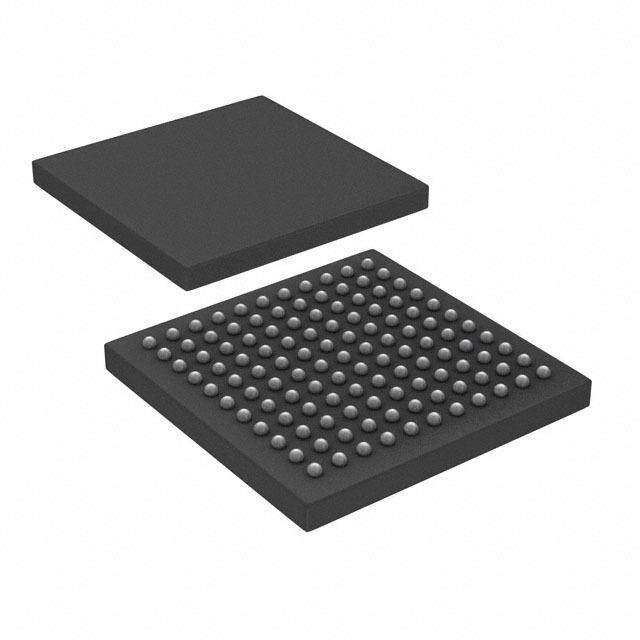
ICGOO电子元器件商城为您提供TSB83AA23ZAY由Texas Instruments设计生产,在icgoo商城现货销售,并且可以通过原厂、代理商等渠道进行代购。 TSB83AA23ZAY价格参考。Texas InstrumentsTSB83AA23ZAY封装/规格:接口 - 控制器, IEEE 1394 连接层控制器 IEEE 1394-1995, 1394a-2000, OHCI, Firewire™, i.Link™ PCI 接口 167-NFBGA(12x12)。您可以下载TSB83AA23ZAY参考资料、Datasheet数据手册功能说明书,资料中有TSB83AA23ZAY 详细功能的应用电路图电压和使用方法及教程。
| 参数 | 数值 |
| 产品目录 | 集成电路 (IC)半导体 |
| 描述 | IC IEEE 1394B-2002 LLC 167-NFBGA1394 接口集成电路 Integr OHCI Link & 3Port S800 Phy |
| 产品分类 | |
| 品牌 | Texas Instruments |
| 产品手册 | |
| 产品图片 | |
| rohs | 符合RoHS无铅 / 符合限制有害物质指令(RoHS)规范要求 |
| 产品系列 | 1394 接口集成电路,Texas Instruments TSB83AA23ZAY- |
| 数据手册 | |
| 产品型号 | TSB83AA23ZAY |
| 产品 | 1394a, 1394b |
| 产品目录页面 | |
| 产品种类 | 1394 接口集成电路 |
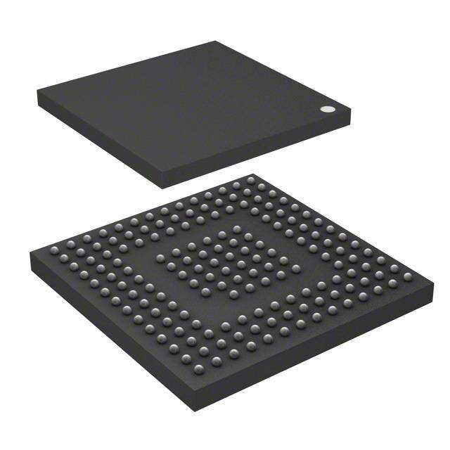
| 供应商器件封装 | 167-NFBGA(12x12) |
| 其它名称 | 296-22860 |
| 功能 | 连接层控制器 |
| 包装 | 托盘 |
| 协议 | IEEE 1394 |
| 商标 | Texas Instruments |
| 安装风格 | SMD/SMT |
| 定时器数量 | 1 |
| 封装 | Tray |
| 封装/外壳 | 167-LFBGA |
| 封装/箱体 | nFBGA-167 |
| 工作温度 | 0°C ~ 70°C |
| 工作温度范围 | 0 C to + 70 C |
| 工作电源电压 | 3.3 V |
| 工厂包装数量 | 160 |
| 接口 | PCI |
| 接口类型 | PCI, Serial |
| 描述/功能 | INTEGRATED IEEE-1394.B OHCI LINK AND 3 PORT S800 PHY |
| 数据总线宽度 | 32 bit |
| 数据速率 | 800 Mb/s |
| 最大工作温度 | + 70 C |
| 最小工作温度 | 0 C |
| 标准 | IEEE 1394-1995, 1394a-2000, OHCI, Firewire™, i.Link™ |
| 标准包装 | 160 |
| 电压-电源 | 3 V ~ 3.6 V |
| 电流-电源 | 120mA |
| 电源电流 | 91 mA |
| 类型 | OHCI Link with Phy |
| 系列 | TSB83AA23 |
| 视频文件 | http://www.digikey.cn/classic/video.aspx?playerID=32016589001&width=966&height=546&playlistlisttabs=32229534001&featuredvideoid=30089576001 |


- 商务部:美国ITC正式对集成电路等产品启动337调查
- 曝三星4nm工艺存在良率问题 高通将骁龙8 Gen1或转产台积电
- 太阳诱电将投资9.5亿元在常州建新厂生产MLCC 预计2023年完工
- 英特尔发布欧洲新工厂建设计划 深化IDM 2.0 战略
- 台积电先进制程称霸业界 有大客户加持明年业绩稳了
- 达到5530亿美元!SIA预计今年全球半导体销售额将创下新高
- 英特尔拟将自动驾驶子公司Mobileye上市 估值或超500亿美元
- 三星加码芯片和SET,合并消费电子和移动部门,撤换高东真等 CEO
- 三星电子宣布重大人事变动 还合并消费电子和移动部门
- 海关总署:前11个月进口集成电路产品价值2.52万亿元 增长14.8%


PDF Datasheet 数据手册内容提取
TSB83AA23 IEEE Std 1394b-2002 PHY and OHCI Link Device Data Manual LiteratureNumber:SLLU099B AUGUST2007–RevisedFebruary2008 PRODUCTIONDATAinformationiscurrentasofpublicationdate. Products conform to specifications per the terms of the Texas Instruments standard warranty. Production processing does not necessarilyincludetestingofallparameters.
TSB83AA23 IEEE Std 1394b-2002 PHY and OHCI Link Device SLLU099B–AUGUST2007–REVISEDFEBRUARY2008 Contents 1 Introduction......................................................................................................................... 9 1.1 Features....................................................................................................................... 9 1.2 Description.................................................................................................................. 10 1.3 TerminalAssignments..................................................................................................... 14 1.3.1 TopView.......................................................................................................... 14 1.3.2 BottomView...................................................................................................... 15 1.3.3 SignalsSortedbyTerminalNumber..................................................................................... 16 1.3.4 SignalsSortedbyName .................................................................................................. 17 1.3.5 TerminalFunctions......................................................................................................... 18 2 ElectricalCharacteristics..................................................................................................... 26 2.1 AbsoluteMaximumRatings............................................................................................... 26 2.2 RecommendedOperatingConditions................................................................................... 26 2.3 ElectricalCharacteristics,PHYDriver................................................................................... 28 2.4 ElectricalCharacteristics,PHYReceiver................................................................................ 28 2.5 ElectricalCharacteristics,General....................................................................................... 29 2.6 ThermalCharacteristics................................................................................................... 29 2.7 SwitchingCharacteristicsforPHYPortion.............................................................................. 30 2.8 SwitchingCharacteristicsforPCIInterface............................................................................. 30 3 PHYSectionRegisterConfiguration..................................................................................... 31 4 PHYSectionApplicationInformation.................................................................................... 37 4.1 Power-ClassProgramming ............................................................................................... 37 4.2 Power-UpReset ........................................................................................................... 39 4.3 CrystalOscillatorSelection............................................................................................... 39 4.4 BusReset................................................................................................................... 40 5 PrinciplesofOperation(IEEEStd1394b-2002Interface)......................................................... 42 5.1 LLCSectionServiceRequest............................................................................................ 43 5.2 StatusTransfer............................................................................................................. 46 5.3 Receive...................................................................................................................... 48 5.4 Transmit..................................................................................................................... 51 6 TSB83AA23LinkLayerControllerProgrammingModel.......................................................... 53 6.1 PCIConfigurationRegisters.............................................................................................. 53 6.1.1 VendorIDRegister.............................................................................................. 54 6.1.2 DeviceIDRegister.............................................................................................. 54 6.1.3 CommandRegister.............................................................................................. 54 6.1.4 StatusRegister .................................................................................................. 55 6.1.5 RevisionIDRegister............................................................................................ 56 6.1.6 ClassCodeRegister............................................................................................ 57 6.1.7 CacheLineSizeRegister...................................................................................... 58 6.1.8 LatencyTimerRegister......................................................................................... 58 6.1.9 HeaderTypeRegister .......................................................................................... 58 6.1.10 Built-InSelf-Test(BIST)Register.............................................................................. 59 6.1.11 OHCIBaseAddressRegister.................................................................................. 59 6.1.12 TIExtensionBaseAddressRegister......................................................................... 60 6.1.13 CardBusCISBaseAddressRegister......................................................................... 60 6.1.14 CardBusCISPointerRegister................................................................................. 61 6.1.15 SubsystemVendorIDRegister................................................................................ 62 6.1.16 SubsystemIDRegister......................................................................................... 62 6.1.17 PowerManagementCapabilitiesPointerRegister.......................................................... 62 6.1.18 InterruptLineRegister.......................................................................................... 63 6.1.19 InterruptPinRegister........................................................................................... 63 2 Contents SubmitDocumentationFeedback
TSB83AA23 IEEE Std 1394b-2002 PHY and OHCI Link Device SLLU099B–AUGUST2007–REVISEDFEBRUARY2008 6.1.20 MinimumGrantRegister........................................................................................ 63 6.1.21 MaximumLatencyRegister.................................................................................... 64 6.1.22 OHCIControlRegister.......................................................................................... 64 6.1.23 CapabilityIDRegister........................................................................................... 65 6.1.24 Next-ItemPointerRegister..................................................................................... 65 6.1.25 PowerManagementCapabilitiesRegister................................................................... 65 6.1.26 PowerManagementControlandStatusRegister........................................................... 66 6.1.27 PowerManagementExtensionRegister..................................................................... 67 6.1.28 PowerManagementDataRegister........................................................................... 67 6.1.29 MultifunctionSelectRegister................................................................................... 68 6.1.30 MiscellaneousConfigurationRegister........................................................................ 68 6.1.31 LLCSectionEnhancementControlRegister................................................................ 70 6.1.32 SubsystemAccessRegister................................................................................... 72 6.1.33 GPIOControlRegister.......................................................................................... 72 6.2 OHCIRegisters............................................................................................................. 73 6.2.1 OHCIVersionRegister......................................................................................... 75 6.2.2 GUIDROMRegister............................................................................................ 75 6.2.3 AsynchronousTransmitRetriesRegister.................................................................... 76 6.2.4 CSRDataRegister.............................................................................................. 77 6.2.5 CSRCompareDataRegister.................................................................................. 77 6.2.6 CSRControlRegister........................................................................................... 77 6.2.7 ConfigurationROMHeaderRegister......................................................................... 78 6.2.8 BusIdentificationRegister...................................................................................... 78 6.2.9 BusOptionsRegister........................................................................................... 78 6.2.10 GUIDHighRegister............................................................................................. 79 6.2.11 GUIDLowRegister.............................................................................................. 80 6.2.12 ConfigurationROMMappingRegister........................................................................ 80 6.2.13 PostedWriteAddressLowRegister.......................................................................... 80 6.2.14 PostedWriteAddressHighRegister.......................................................................... 81 6.2.15 OHCIVendorIDRegister...................................................................................... 81 6.2.16 HostControllerControlRegister............................................................................... 82 6.2.17 Self-IDBufferPointerRegister................................................................................. 83 6.2.18 Self-IDCountRegister.......................................................................................... 84 6.2.19 IsochronousReceiveChannelMaskHighRegister........................................................ 85 6.2.20 IsochronousReceiveChannelMaskLowRegister......................................................... 85 6.2.21 InterruptEventRegister........................................................................................ 86 6.2.22 InterruptMaskRegister......................................................................................... 88 6.2.23 IsochronousTransmitInterruptEventRegister.............................................................. 90 6.2.24 IsochronousTransmitInterruptMaskRegister.............................................................. 91 6.2.25 IsochronousReceiveInterruptEventRegister.............................................................. 91 6.2.26 IsochronousReceiveInterruptMaskRegister............................................................... 92 6.2.27 InitialBandwidthAvailableRegister........................................................................... 92 6.2.28 InitialChannelsAvailableHighRegister...................................................................... 92 6.2.29 InitialChannelsAvailableLowRegister...................................................................... 93 6.2.30 FairnessControlRegister...................................................................................... 93 6.2.31 LLCSectionControlRegister.................................................................................. 94 6.2.32 NodeIdentificationRegister.................................................................................... 94 6.2.33 PHYLayerControlRegister.................................................................................... 95 6.2.34 IsochronousCycleTimerRegister............................................................................ 96 6.2.35 AsynchronousRequestFilterHighRegister................................................................. 96 6.2.36 AsynchronousRequestFilterLowRegister.................................................................. 97 6.2.37 PhysicalRequestFilterHighRegister........................................................................ 97 6.2.38 PhysicalRequestFilterLowRegister......................................................................... 98 Contents 3
TSB83AA23 IEEE Std 1394b-2002 PHY and OHCI Link Device SLLU099B–AUGUST2007–REVISEDFEBRUARY2008 6.2.39 PhysicalUpperBoundRegister(OptionalRegister)........................................................ 99 6.2.40 AsynchronousContextControlRegister..................................................................... 99 6.2.41 AsynchronousContextCommandPointerRegister....................................................... 100 6.2.42 IsochronousTransmitContextControlRegister........................................................... 100 6.2.43 IsochronousTransmitContextCommandPointerRegister.............................................. 101 6.2.44 IsochronousReceiveContextControlRegister............................................................ 102 6.2.45 IsochronousReceiveContextCommandPointerRegister............................................... 104 6.2.46 IsochronousReceiveContextMatchRegister............................................................. 104 6.3 TIExtensionRegisters................................................................................................... 105 6.3.1 DVTimestampEnhancements............................................................................... 105 6.3.2 MPEG2TimestampProcedure............................................................................... 106 6.3.3 IsochronousReceiveDigitalVideoEnhancements....................................................... 106 6.3.4 IsochronousReceiveDigitalVideoEnhancementsRegister............................................. 106 6.3.5 LinkEnhancementRegister.................................................................................. 107 6.3.6 TimestampOffsetRegister................................................................................... 110 7 General-PurposeInput/Output(GPIO)Interface.................................................................... 111 8 SerialEEPROMInterface................................................................................................... 112 4 Contents SubmitDocumentationFeedback
TSB83AA23 IEEE Std 1394b-2002 PHY and OHCI Link Device SLLU099B–AUGUST2007–REVISEDFEBRUARY2008 List of Figures 2-1 TestLoadDiagram................................................................................................................ 30 2-2 SetupandHoldTimeWaveformsforDx,CTLx,andLREQInputs........................................................ 30 2-3 DxandCTLxOutputDelayRelativetoxCLKWaveforms................................................................... 31 4-1 TypicalTwistedPairIEEEStd1394a-2000CableConnections............................................................ 38 4-2 TypicalDC-IsolatedOuterShieldTermination................................................................................ 38 4-3 Non-DC-IsolatedOuterShieldTermination.................................................................................... 39 5-1 PHYSection-LLCSectionInterface............................................................................................ 42 5-2 LREQ/PHY_LREQRequestStream............................................................................................ 43 5-3 BusStatusTransfer............................................................................................................... 47 5-4 PINT(PHYSectionInterrupt)Stream.......................................................................................... 47 5-5 NormalPacketReception........................................................................................................ 49 5-6 NormalPacketReceptionWithOptionalBusStatusTransfer.............................................................. 49 5-7 NullPacketReception............................................................................................................ 50 7-1 GPIOLogicDiagram............................................................................................................ 111 ListofFigures 5
TSB83AA23 IEEE Std 1394b-2002 PHY and OHCI Link Device SLLU099B–AUGUST2007–REVISEDFEBRUARY2008 List of Tables 3-1 BaseRegisterConfiguration..................................................................................................... 31 3-2 BaseRegisterFieldDescriptions............................................................................................... 31 3-3 Page-0(Port-Status)RegisterConfiguration.................................................................................. 33 3-4 Page-0(Port-Status)RegisterFieldDescriptions............................................................................. 34 3-5 Page1(VendorID)RegisterConfiguration ................................................................................... 35 3-6 Page1(VendorID)RegisterFieldDescriptions.............................................................................. 36 3-7 Page7(Vendor-Dependent)RegisterConfiguration......................................................................... 36 3-8 Page7(Vendor-Dependent)RegisterFieldDescriptions ................................................................... 36 4-1 PowerClassDescriptions........................................................................................................ 37 5-1 CTLEncodingWhenPHYSectionHasControloftheBus................................................................. 43 5-2 CTLEncodingWhenLLCSectionHasControloftheBus.................................................................. 43 5-3 RequestStreamBitLength...................................................................................................... 44 5-4 Request-TypeEncoding.......................................................................................................... 44 5-5 BusRequest....................................................................................................................... 45 5-6 Bus-RequestFormatEncoding.................................................................................................. 45 5-7 Bus-RequestSpeedEncoding.................................................................................................. 45 5-8 ReadRegisterRequest .......................................................................................................... 45 5-9 WriteRegisterRequest........................................................................................................... 46 5-10 LinkNotificationRequest......................................................................................................... 46 5-11 StatusBits.......................................................................................................................... 47 5-12 PHYStatusTransferEncoding.................................................................................................. 48 5-13 RegisterRead(SolicitedandUnsolicited)PHYStatusTransferEncoding ............................................... 48 5-14 ReceiveSpeedCodesandFormat ............................................................................................ 50 5-15 Link-Request-TypeEncodingDuringPacketTransmission................................................................. 51 5-16 Link-RequestSpeed-CodeEncodingDuringPacketTransmission........................................................ 51 5-17 Link-RequestFormatEncodingDuringPacketTransmission............................................................... 52 5-18 SubactionEnd-NotificationEncodingDuringPacketTransmission........................................................ 52 5-19 FormatTypeDuringGrantCycle............................................................................................... 52 5-20 GrantTypeValuesDuringGrantCycle........................................................................................ 52 5-21 SpeedTypeValuesDuringGrantCycle....................................................................................... 52 6-1 BitFieldAccessTagDescriptions.............................................................................................. 53 6-2 PCIConfigurationRegisterMap................................................................................................ 53 6-3 CommandRegisterDescription................................................................................................. 55 6-4 StatusRegisterDescription...................................................................................................... 56 6-5 RevisionIDRegisterDescription................................................................................................ 56 6-6 ClassCodeRegisterDescription ............................................................................................... 57 6-7 CacheLineSizeRegisterDescription.......................................................................................... 58 6-8 LatencyTimerRegisterDescription............................................................................................ 58 6-9 HeaderTypeRegisterDescription.............................................................................................. 58 6 ListofTables SubmitDocumentationFeedback
TSB83AA23 IEEE Std 1394b-2002 PHY and OHCI Link Device SLLU099B–AUGUST2007–REVISEDFEBRUARY2008 6-10 Built-InSelf-Test(BIST)RegisterDescription................................................................................. 59 6-11 OHCIBaseAddressRegisterDescription..................................................................................... 59 6-12 TIBaseAddressRegisterDescription......................................................................................... 60 6-13 CardBusCISBaseAddressRegisterDescription............................................................................ 61 6-14 CardBusCISPointerRegisterDescription.................................................................................... 61 6-15 SubsystemVendorIDRegisterDescription................................................................................... 62 6-16 SubsystemIDRegisterDescription............................................................................................. 62 6-17 InterruptLineRegisterDescription ............................................................................................. 63 6-18 InterruptLineandPinRegisterDescription ................................................................................... 63 6-19 MinimumGrantRegisterDescription........................................................................................... 63 6-20 MaximumLatencyRegisterDescription ....................................................................................... 64 6-21 OHCIControlRegisterDescription............................................................................................. 64 6-22 CapabilityIDRegisterDescription.............................................................................................. 65 6-23 Next-ItemPointerRegisterDescription........................................................................................ 65 6-24 PowerManagementCapabilitiesRegisterDescription ...................................................................... 66 6-25 PowerManagementControlandStatusRegisterDescription.............................................................. 66 6-26 PowerManagementExtensionRegisterDescription......................................................................... 67 6-27 PowerManagementDataRegisterDescription............................................................................... 67 6-28 MultifunctionSelectRegister.................................................................................................... 68 6-29 MiscellaneousConfigurationRegister.......................................................................................... 69 6-30 LLCSectionEnhancementControlRegisterDescription.................................................................... 71 6-31 SubsystemAccessRegisterDescription....................................................................................... 72 6-32 GPIOControlRegisterDescription............................................................................................. 72 6-33 OHCIRegisterMap............................................................................................................... 73 6-34 OHCIVersionRegisterDescription............................................................................................. 75 6-35 GUIDROMRegisterDescription................................................................................................ 76 6-36 AsynchronousTransmitRetriesRegisterDescription........................................................................ 76 6-37 CSRControlRegisterDescription.............................................................................................. 77 6-38 ConfigurationROMHeaderRegisterDescription............................................................................. 78 6-39 BusOptionsRegisterDescription............................................................................................... 79 6-40 ConfigurationROMMappingRegisterDescription........................................................................... 80 6-41 PostedWriteAddressLowRegisterDescription ............................................................................. 80 6-42 PostedWriteAddressHighRegisterDescription............................................................................. 81 6-43 VendorIDRegisterDescription................................................................................................. 82 6-44 HostControllerControlRegisterDescription.................................................................................. 82 6-45 Self-IDCountRegisterDescription............................................................................................. 84 6-46 IsochronousReceiveChannelMaskHighRegisterDescription............................................................ 85 6-47 IsochronousReceiveChannelMaskLowRegisterDescription............................................................ 85 6-48 InterruptEventRegisterDescription............................................................................................ 87 6-49 InterruptMaskRegisterDescription............................................................................................ 89 6-50 IsochronousTransmitInterruptEventRegisterDescription................................................................. 91 ListofTables 7
TSB83AA23 IEEE Std 1394b-2002 PHY and OHCI Link Device SLLU099B–AUGUST2007–REVISEDFEBRUARY2008 6-51 IsochronousReceiveInterruptEventRegisterDescription.................................................................. 92 6-52 InitialBandwidthAvailableRegisterDescription.............................................................................. 92 6-53 InitialChannelsAvailableHighRegisterDescription......................................................................... 93 6-54 InitialChannelsAvailableHighRegisterDescription......................................................................... 93 6-55 FairnessControlRegisterDescription.......................................................................................... 94 6-56 LLCSectionControlRegisterDescription..................................................................................... 94 6-57 NodeIdentificationRegisterDescription....................................................................................... 95 6-58 PHYLayerControlRegisterDescription....................................................................................... 95 6-59 IsochronousCycleTimerRegisterDescription ............................................................................... 96 6-60 AsynchronousRequestFilterHighRegisterDescription.................................................................... 97 6-61 AsynchronousRequestFilterLowRegisterDescription..................................................................... 97 6-62 PhysicalRequestFilterHighRegisterDescription........................................................................... 98 6-63 PhysicalRequestFilterLowRegisterDescription............................................................................ 98 6-64 AsynchronousContextControlRegisterDescription......................................................................... 99 6-65 AsynchronousContextCommandPointerRegisterDescription.......................................................... 100 6-66 IsochronousTransmitContextControlRegisterDescription.............................................................. 101 6-67 IsochronousReceiveContextControlRegisterDescription............................................................... 103 6-68 IsochronousReceiveContextMatchRegisterDescription ................................................................ 105 6-69 TIExtensionRegisterMap..................................................................................................... 105 6-70 IsochronousReceiveDigitalVideoEnhancementsRegisterDescription................................................ 107 6-71 LinkEnhancementRegisterDescription...................................................................................... 109 6-72 TimestampOffsetRegisterDescription....................................................................................... 110 8-1 SerialEEPROMMap............................................................................................................ 113 8 ListofTables SubmitDocumentationFeedback
TSB83AA23 IEEE Std 1394b-2002 PHY and OHCI Link Device www.ti.com SLLU099B–AUGUST2007–REVISEDFEBRUARY2008 1 Introduction 1.1 Features • FullySupportsProvisionsofIEEEStd • Fail-SafeCircuitrySensesSuddenLossof 1394b-2002Revision1.33+at1-Gigabit PowertotheDeviceandDisablesPortsto SignalingRates EnsureThatTSB83AA23DoesNotLoad • FullySupportsProvisionsofIEEEStd TPBIASofAnyConnectedDeviceandBlocks AnyLeakageFromthePortBacktoPower 1394a-2000andIEEEStd1394-1995for Plane High-PerformanceSerialBus • IEEEStd1394a-2000-Compliant • FullyInteroperableWithFirewire™,i.LINK™, Common-ModeNoiseFilteronIncomingBias andSB1394ImplementationsofIEEEStd1394 DetectCircuittoFilterOutCrosstalkNoise • ProvidesThreeFullyBackward-Compatible, • PortProgrammabletoForceIEEEStd (IEEEStd1394a-2000FullyCompliant) 1394a-2000ModetoAllowUseofIEEEStd BilingualIEEEStd1394b-2002CablePortsat 1394a-2000Connectors(IEEEStd1394b-2002 upto800MegabitsperSecond(Mbps) SignalingMustNotBePutAcrossIEEEStd • FullIEEEStd1394a-2000SupportIncludes: 1394a-2000ConnectorsorCables) – ConnectionDebounce • 3.3-Vand5-VPCISignalingEnvironments – ArbitratedShortReset • Serial-BusDataRatesof100Mbps,200Mbps, – MultispeedConcatenation 400Mbps,and800Mbps – ArbitrationAcceleration • PhysicalWritePostingofuptoThree – Fly-ByConcatenation OutstandingTransactions – PortDisable/Suspend/Resume • SerialROMorBootROMInterfaceSupports • ExtendedResumeSignalingforCompatibility 2-WireSerialEEPROMDevices WithLegacyDigitalVideo(DV)Devices • 33-MHz/32-BitPCIInterface • Power-DownFeaturestoConserveEnergyin Battery-PoweredApplications • MultifunctionTerminal(MFUNCTerminal1): • Low-PowerSleepMode – PCI_CLKRUNProtocolPerPCIMobile DesignGuide • FullyCompliantWithOpenHostController – General-PurposeI/O(GPIO) Interface(OHCI)Requirements – CYCLEIN/CYCLEOUTforExternalCycle • CablePowerPresenceMonitoring TimerControlforCustomized • CablePortsMonitorLineConditionsforActive Synchronization ConnectiontoRemoteNode • PCIBurstTransfersandDeepFIFOsto • RegisterBitsGiveSoftwareControlof TolerateLargeHostLatency ContenderBit,Power-ClassBits,LinkActive – TransmitFIFO—5KAsynchronous ControlBit,andIEEEStd1394a-2000Features – TransmitFIFO—2KIsochronous • InteroperableWithOther1394PhysicalLayers – ReceiveFIFO—2KAsynchronous (PHYs)Using1.8-V,3.3-V,and5-VSupplies – ReceiveFIFO—2KIsochronous • Low-Jitter,ExternalCrystalOscillatorProvides • D0,D1,D2,andD3PowerStatesandPME TransmitandReceiveDataat100/200/400/800 EventsPerPCIBusPowerManagement MbpsandLink-LayerController(LLC)Clockat InterfaceSpecification 49.152MHzand98.304MHz • ProgrammableAsynchronousTransmit • SeparateBias(TPBIAS)forEachPort Threshold • SoftwareDeviceReset(SWR) • IsochronousReceiveDual-BufferMode • Out-of-OrderPipeliningforAsynchronous TransmitRequests Pleasebeawarethatanimportantnoticeconcerningavailability,standardwarranty,anduseincriticalapplicationsofTexas Instrumentssemiconductorproductsanddisclaimerstheretoappearsattheendofthisdocument. OHCI-LynxisatrademarkofTexasInstruments. FirewireisatrademarkofAppleComputer,Inc. i.LINKisatrademarkofSonyKabushikiKaishaTASonyCorporation. Allothertrademarksarethepropertyoftheirrespectiveowners. PRODUCTIONDATAinformationiscurrentasofpublicationdate. Copyright©2007–2008,TexasInstrumentsIncorporated Products conform to specifications per the terms of the Texas Instruments standard warranty. Production processing does not necessarilyincludetestingofallparameters.
TSB83AA23 IEEE Std 1394b-2002 PHY and OHCI Link Device www.ti.com SLLU099B–AUGUST2007–REVISEDFEBRUARY2008 • Initial-Bandwidth-Availableand • DigitalVideoandAudioPerformance Initial-Channels-AvailableRegisters Enhancements 1.2 Description The TSB83AA23 is an integrated IEEE Std 1394b-2002 link-layer controller (LLC) design and physical layer (PHY) design combined in a single package to meet the demanding requirements of today’s 1394 bus applications. The TSB83AA23 device is capable of exceptional 800-Mbps performance; thus, providing the throughput and bandwidth to move data efficiently and quickly between the PCI and 1394 buses. The TSB83AA23 device also provides outstanding ultralow power operation and intelligent power-management capabilities. The device provides the IEEE 1394 LLC function and PHY function and iscompatiblewith100-Mbps,200-Mbps,400-Mbps,and800-Mbpsserial-busdatarates. The TSB83AA23 operates as the interface between 33-MHz/32-bit PCI local bus and an IEEE Std 1394a-2000 or IEEE Std 1394b-2002 serial-bus interface. It is capable of supporting serial data rates at 98.304, 196.608, 393.216, 491.52, or 786.432 Mbps (referred to as S100, S200, S400, S400B, or S800 speeds, respectively). When acting as a PCI bus master, the TSB83AA23 device is capable of multiple cache-line bursts of data, which can transfer at 132M bytes/s for 32-bit transfers after connecting to the memorycontroller. Due to the high throughput potential of the TSB83AA23 device, it possible to encounter large PCI and legacy 1394 bus latencies, which can cause the 1394 data to be overrun. To overcome this potential problem, the TSB83AA23 implements deep transmit and receive FIFOs (see Section 1.1, Features, for FIFO size information) to buffer the 1394 data, thus, preventing possible problems due to bus latency. This also ensures that the device can transmit and receive sustained maximum-size isochronous or asynchronousdatapayloadsatS800. The TSB83AA23 LLC section implements other performance enhancements to improve overall performance of the device, such as a highly-tuned physical data path for enhanced SBP-2 performance, physicalpostwritingbuffers,multipleisochronouscontexts,andadvancedinternalarbitration. The TSB83AA23 LLC section also implements hardware enhancements to better support digital video (DV) and MPEG data stream reception and transmission. These enhancements are enabled through the isochronous receive digital video enhancements register at TI extension offset A80h (see Section 6.3.4, Isochronous Receive Digital Video Enhancements Register). These enhancements include automatic time-stamp insertion for transmitted DV and MPEG-formatted streams, and common isochronous packet (CIP)headerstrippingforreceivedDVstreams. The CIP format is defined by the IEC 61883-1:1998 specification. The enhancements to the isochronous data contexts are implemented as hardware support for the synchronization time stamp for both DV and audio/video CIP formats. The TSB83AA23 device supports modification of the synchronization time-stamp field to ensure that the value inserted via software is not stale — that is, less than the current cycle timer whenthepacketistransmitted. The TSB83AA23 performance and enhanced throughput make it an excellent choice for today’s 1394 PC market; however, portable, mobile, and even desktop PC power-management schemes continue to require devices to use less and less power, and TI’s 1394 product line has continued to raise the bar by providing the lowest-power 1394 devices in the industry. The TSB83AA23 device represents the next evolution of TI commitment to meet the challenge of power-sensitive applications. The TSB83AA23 device has ultralow operational power requirements and intelligent power-management capabilities that allow it to conserve power autonomously based on the device usage. The TSB83AA23 LLC section fully supports D0, D1, D2, and D3 power states, as specified in the PC 2001 Design Guide requirements and the hot/cold PCI Power Management Specification. PME wake-event support is subject to operating-system support andimplementation. 10 Introduction SubmitDocumentationFeedback
TSB83AA23 IEEE Std 1394b-2002 PHY and OHCI Link Device www.ti.com SLLU099B–AUGUST2007–REVISEDFEBRUARY2008 As required by the 1394 Open Host Controller Interface Specification (OHCI) and IEEE Std 1394a-2000, internal control registers are memory mapped and nonprefetchable. The PCI configuration header is accessed through configuration cycles as specified by the PCI Local Bus Specification, and provides plug-and-play (PnP) compatibility. Furthermore, the TSB83AA23 LLC section is fully compliant with the latest PCI Local Bus Specification, PCI Bus Power Management Interface Specification, IEEE Std 1394b-2002,IEEEStd1394a-2000,and1394OpenHostControllerInterfaceSpecification. TheTSB83AA23PHYsectionprovidesthedigitalandanalog transceiver functions needed to implement a three-port node in a cable-based IEEE 1394 network. Each cable port incorporates two differential line transceivers. The transceivers include circuitry to monitor the line conditions as needed for determining connectionstatus,forinitializationandarbitration,andforpacketreceptionandtransmission. The TSB83AA23 is powered by multiple voltage supplies, 3.3-V supplies for I/O and the LLC section, and a core voltage supply for the PHY section. The core voltage supply is supplied to the PLLVDD_CORE and DVDD_CORE terminals in accordance with the requirements in the recommended operating conditions. The PLLVDD_CORE terminals must be separated from the DVDD_CORE terminals, the PLLVDD_CORE terminals are decoupled with 1-m F and smaller decoupling capacitors, and the DVDD_CORE terminals separatelydecoupledwith1-m Fandsmallerdecouplingcapacitors.TheseparationbetweenDVDD_CORE andPLLVDD_COREcanbeimplementedbyseparatepower-supply rails, or by a single power-supply rail, where the DVDD_CORE and PLLVDD_CORE are separated by a filter network to keep noise from the PLLVDD_CORE supply. In addition, REG_EN must be asserted low to enable the internal voltage regulator for the LLC section. If REG_EN is not pulled low, the a 1.8-V power rail must be applied to the REG18pins. The TSB83AA23 requires an external 98.304-MHz crystal oscillator to generate a reference clock. The external clock drives an internal phase-locked loop (PLL), which generates the required reference signal. This reference signal provides the clock signals that control transmission of the outbound encoded information. The power-down (PD) function, when enabled by asserting the PD terminal high, stops operationofthePLL. Data bits to be transmitted through the cable ports are latched internally, combined serially, encoded, and transmitted at 98.304, 196.608, 393.216, 491.52, or 983.04 Mbps (referred to as S100, S200, S400, S400B,orS800speed,respectively)astheoutboundinformationstream. To ensure that the TSB83AA23 conforms to the IEEE Std 1394b-2002 standard, the BMODE terminal mustbeasserted. NOTE TheBMODEterminaldoesnotselectthecable-interfacemodeofoperation.TheBMODE terminal selects the internal PHY section-LLC section interface mode of operation and affects the arbitration modes on the cable. BMODE must be pulled high during normal operation. The cable interface can follow either the IEEE Std 1394a-2000 protocol or the IEEE Std 1394b-2002 protocol on all ports. The mode of operation is determined by the interface capabilities of the ports being connected. When any of the ports are connected to an IEEE Std 1394a-2000-compliant device, the cable interfaceonthatportoperatesintheIEEEStd1394a-2000 data-strobe mode at a compatible S100, S200, or S400 speed. When a bilingual port is connected to an IEEE Std 1394b-2002-compliant node, the cable interface on that port operates per the IEEE Std 1394b-2002 standard at S400B or S800 speed. The TSB83AA23 automatically determines the correct cable interface connection method for the bilingual ports. SubmitDocumentationFeedback Introduction 11
TSB83AA23 IEEE Std 1394b-2002 PHY and OHCI Link Device www.ti.com SLLU099B–AUGUST2007–REVISEDFEBRUARY2008 To operate a port as an IEEE Std 1394b-2002 bilingual port, the data-strobe-only terminal for the port (DS0 or DS1) must be pulled to ground through a 1-kW resistor. The port must be operated in the IEEE Std 1394b-2002 bilingual mode when an IEEE Std 1394b-2002 bilingual or an IEEE Std 1394b-2002 Beta-only connector is connected to the port. To operate the port as an IEEE Std 1394a-2000-only port, the data-strobe-only terminal (DS0 or DS1) must be pulled to 3.3-V V through a 1-kW resistor. The only CC time the port must be forced to the data-strobe-only mode is if the port is connected to an IEEE Std 1394a-2000 connector (either 6 pin, which is recommended, or 4 pin). This mode is provided to ensure thatIEEEStd1394b-2002signalingisneversentacrossanIEEEStd1394a-2000cable. During packet reception, the serial data bits are split into 2-, 4-, or 8-bit parallel streams by the PHY section and sent to the link-layer controller (LLC) section. The received data is also transmitted (repeated) ontheotherconnectedandactivecableports. Both the twisted pair A (TPA) and the twisted pair B (TPB) cable interfaces incorporate differential comparators to monitor the line states during initialization and arbitration when connected to an IEEE Std 1394a-2000-compliant device. The outputs of these comparators are used by the internal logic to determine the arbitration status. The TPA channel monitors the incoming cable common-mode voltage. The value of this common-mode voltage is used during IEEE Std 1394a-2000-mode arbitration and sets the speed of the next packet transmission. In addition, the TPB channel monitors the incoming cable common-mode voltage on the TPB pair for the presence of the remotely supplied twisted pair bias (TPBIAS)voltage. When connected to an IEEE Std 1394a-2000-compliant node, the TSB83AA23 PHY section provides a 1.86-V nominal bias voltage at the TPBIAS terminal for port termination. The PHY section contains three independent TPBIAS circuits (one for each port). This bias voltage, when seen through a cable by a remote receiver, indicates the presence of an active connection. This bias voltage source must be stabilizedbyanexternalfiltercapacitorof1m F. The line drivers in the TSB83AA23 PHY section are designed to work with external 112-W termination resistor networks to match the 110-W cable impedance. One termination network is required at each end of a twisted-pair cable. Each network is composed of a pair of series-connected 56-W resistors. The midpoint of the pair of resistors that is connected to the TPA terminals is connected to its corresponding TPBIAS voltage terminal. The midpoint of the pair of resistors that is directly connected to the TPB terminals is coupled to ground through a parallel RC network, with recommended values of 5 kW and 270 pF. The values of the external line-termination resistors are selected to meet the standard specifications when connected in parallel with the internal receiver circuits. A precision external resistor connected between the R0 and R1 terminals sets the driver output current, along with other internal operatingcurrents. When the power supply of the TSB83AA23 is off while the twisted-pair cables are connected, the TSB83AA23 transmitter and receiver circuitry present to the cable a high-impedance signal that does not loadthedeviceattheotherendofthecable. When the TSB83AA23 PHY section is used without one or more of the ports brought out to a connector, the twisted-pair terminals of the unused ports must be terminated for reliable operation. For each unused port, the port must be forced to the IEEE Std 1394a-2000-only mode (data-strobe-only mode), after which the TPB+ and TPB– terminals can be tied together and then pulled to ground; or the TPB+ and TPB– terminals can be connected to the suggested normal termination network. The TPA+ and TPA– terminals of an unused port can be left unconnected. The TPBIAS terminal can be connected through a 1-m F capacitortogroundorleftunconnected. The TESTM, TESTW, SE, and SM terminals are used to set up various manufacturing test conditions. For normal operation, the TESTM and TESTW terminals must be connected to V through a 1-kW resistor. DD TheSEandSMterminalsmustbetiedtogroundthrougha1-kW resistor. 12 Introduction SubmitDocumentationFeedback
TSB83AA23 IEEE Std 1394b-2002 PHY and OHCI Link Device www.ti.com SLLU099B–AUGUST2007–REVISEDFEBRUARY2008 Three package terminals are used as inputs to set the default value for three configuration status bits in the self-ID packet. They can be pulled high through a 1-kW resistor or hardwired low as a function of the equipment design. The PC0, PC1, and PC2 terminals indicate the default power class status for the node (the need for power from the cable or the ability to supply power to the cable). The contender bit in the PHYregistersetindicates that the node is a contender either for the isochronous resource manager (IRM) or for the bus manager (BM). On the TSB83AA23, this bit can be set only by a write to the PHY register set. If a node is to be a contender for IRM or BM, the node software must set this bit in the PHY register set. The LPS (link power status) terminal of the PHY section works with the LKON terminal to manage the power usage in the node. The PHY_LPS signal from the LLC section is used with the LCtrl bit (see Section 1.3.5) to indicate the active/power status of the LLC section. The LPS signal also resets, disables, and initializes the PHY section-LLC section interface (the state of the PHY section-LLC section interface is controlled solely by the LPS input, regardless of the state of the LCtrl bit). The LPS terminal of the PHY sectionmustbeconnectedtothePHY_LPSterminaloftheLLCsectionduringnormaloperation. The LPS input is considered inactive if it remains low for more than the LPS_RESET time (see the LPS terminal definition) and is considered active otherwise. When the PHY section detects that the LPS input is inactive, the PHY section-LLC section interface is placed into a low-power reset state in which the CTL and D outputs are held in the logic 0 state and the LREQ input is ignored; however, the PCLK output remains active. If the LPS input remains low for more than the LPS_DISABLE time (see the LPS terminal definition),thePHYsection-LLC section interface is put into a low-power disabled state in which the PCLK output is also held inactive. The TSB83AA23 continues the necessary PHY repeater functions required for normal network operation, regardless of the state of the PHY section-LLC section interface. When the interface is in the reset or disabled state and the LPS input is again observed active, the PHY section initializes the interface and returns to normal operation. The PHY section-LLC section interface is also held in the disabled state during hardware reset. When the LPS terminal is returned to an active state after being sensed as having entered the LPS_DISABLE time, the TSB83AA23 issues a bus reset. This broadcasts the node self-ID packet, which contains the updated L bit state (the PHY section and LLC sectionnowbeingaccessible). The PHY section uses the LKON terminal to notify the LLC section to power up and become active. When activated,theoutputLKONsignalisasquarewave.ThePHYsectionactivatestheLKONoutputwhenthe LLC section is inactive and a wake-up event occurs. The LLC section is considered inactive when either the LPS input is inactive, as previously described, or the LCtrl bit is cleared to 0. A wake-up event occurs when a link-on PHY packet addressed to this node is received, or conditionally when a PHY interrupt occurs. The PHY section deasserts the LKON output when the LLC section becomes active (both LPS sensed as active and the LCtrl bit set to 1). The PHY section also deasserts the LKON output when a bus reset occurs, unless a PHY interrupt condition exists, which would otherwise cause LKON to be active. If the TSB83AA23 is power cycled and the power class is 0 through 4, the PHY section asserts LKON for approximately167m soruntilboththeLPSisactiveandtheLCtrlbitis1. SubmitDocumentationFeedback Introduction 13
TSB83AA23 IEEE Std 1394b-2002 PHY and OHCI Link Device www.ti.com SLLU099B–AUGUST2007–REVISEDFEBRUARY2008 1.3 Terminal Assignments 1.3.1 Top View A B C D E F G H J K L M N P 14 PCI_AD17 PCI_AD18 PCI_AD21 PCI_AD22 PCI_AD23 PCI_AD24 PCI_AD27 PCI_AD28 PCI_AD30 PCI_PME PCI_CLK PC2 PCI_RST PCI_INTA 13 PCI_AD16 PCI_AD19 PCI_AD20 PCI_IDSEL PCI_C/BE3 PCI_AD25 PCI_AD26 PCI_AD29 PCI_AD31 PCI_REQ PCI_GNT PC1 SDA TPA2+ 12 FRPCAMI_E PCI_C/BE2 PINT PHY_PINT CNA PD TESTM RESET BMODE (VTREESGT_WPD) PC0 G_RST SCL TPA2- 11 PCI_ PCI_IRDY LPS MFUNC REG_EN TPB2+ DEVSEL 10 PCI_STOP PCI_TRDY PHY_LPS DVDD_3.3 DVDD_ VCCP REG18 GND AVDD_3.3 TPBIAS2 GND TPB2- CORE 09 PCI_PERR LKON/DS2 PHY_LINKON VCC GND GND GND GND AVDD_3.3 TPBIAS1 GND TPA1+ 08 PCI_SERR LREQ PHY_LREQ VCC GND GND GND GND VCC TPBIAS0 GND TPA1- 07 PCI_C/BE1 PCLK PHY_PCLK VCC GND GND GND GND VCC PHY_CTL0 GND TPB1+ -CTL0 06 PCI_PAR LCLK PHY_LCLK DVDD_3.3 GND GND GND VCC AVDD_3.3 PHY_CTL1 GND TPB1- -CTL1 05 PCI_AD15 PCI_AD14 PCI_C/BE0 DVDD_ REG18 VCCP VCC AVDD_3.3 PHY_D0-D0 GND TPA0+ CORE 04 PCI_AD12 PCI_AD13 PCI_ACK64 PHY_D1-D1 GND TPA0- 03 PCI_AD11 PCI_AD6 PCI_AD5 PCI_AD4 PCI_ PLLVDD_ PLLVDD_3.3 CPS GND GND PHY_D7-D7 PHY_D2-D2 GND TPB0+ REQ64 CORE 02 PCI_AD10 PCI_AD7 PCI_AD2 PCI_AD3 AVDD_3.3 PLLGND DS1 DS0 SE GND PHY_D6-D6 PHY_D3-D3 GND TPB0- 01 PCI_AD9 PCI_AD8 PCI_AD1 PCI_AD0 R1 R0 RSVD (XO) XI SM GND PHY_D5-D5 PHY_D4-D4 GND GND 14 Introduction SubmitDocumentationFeedback
TSB83AA23 IEEE Std 1394b-2002 PHY and OHCI Link Device www.ti.com SLLU099B–AUGUST2007–REVISEDFEBRUARY2008 1.3.2 Bottom View P GND TPB0- TPB0+ TPA0- TPA0+ TPB1- TPB1+ TPA1- TPA1+ TPB2- TPB2+ TPA2- TPA2+ PCI_INTA N GND GND GND GND GND GND GND GND GND GND REG_EN SCL SDA PCI_RST M PHY_D4-D4 PHY_D3-D3 PHY_D2-D2 PHY_D1-D1 PHY_D0-D0 PHY_CTL1 PHY_CTL0 TPBIAS0 TPBIAS1 TPBIAS2 MFUNC G_RST PC1 PC2 -CTL1 -CTL0 L PHY_D5-D5 PHY_D6-D6 PHY_D7-D7 PC0 PCI_GNT PCI_CLK K GND GND GND AVDD_3.3 AVDD_3.3 VCC VCC AVDD_3.3 AVDD_3.3 (VTREESGT_WPD) PCI_REQ PCI_PME J SM SE GND VCC VCC GND GND GND GND BMODE PCI_AD31 PCI_AD30 H XI DS0 CPS VCCP GND GND GND GND REG18 RESET PCI_AD29 PCI_AD28 G RSVD (XO) DS1 PLLVDD_3.3 REG18 GND GND GND GND VCCP TESTM PCI_AD26 PCI_AD27 F R0 PLLGND PLCLOVRDED_ DCVODRDE_ GND GND GND GND DCVODRDE_ PD PCI_AD25 PCI_AD24 E R1 AVDD_3.3 PCI_ DVDD_3.3 VCC VCC VCC DVDD_3.3 CNA PCI_C/BE3 PCI_AD23 REQ64 D PCI_AD0 PCI_AD3 PCI_AD4 PHY_PINT PCI_IDSEL PCI_AD22 C PCI_AD1 PCI_AD2 PCI_AD5 PCI_ACK64 PCI_C/BE0 PHY_LCLK PHY_PCLK PHY_LREQ PHY_LINKON PHY_LPS LPS PINT PCI_AD20 PCI_AD21 B PCI_AD8 PCI_AD7 PCI_AD6 PCI_AD13 PCI_AD14 LCLK PCLK LREQ LKON/DS2 PCI_TRDY PCI_IRDY PCI_C/BE2 PCI_AD19 PCI_AD18 A PCI_AD9 PCI_AD10 PCI_AD11 PCI_AD12 PCI_AD15 PCI_PAR PCI_C/BE1 PCI_SERR PCI_PERR PCI_STOP PCI_ PCI_ PCI_AD16 PCI_AD17 DEVSEL FRAME 01 02 03 04 05 06 07 08 09 10 11 12 13 14 SubmitDocumentationFeedback Introduction 15
TSB83AA23 IEEE Std 1394b-2002 PHY and OHCI Link Device www.ti.com SLLU099B–AUGUST2007–REVISEDFEBRUARY2008 1.3.3 Signals Sorted by Terminal Number Terminal SignalName Terminal SignalName Terminal SignalName Terminal SignalName Number Number Number Number A01 PCI_AD9 D01 PCI_AD0 H02 DS0 M02 PHY_D3-D3 A02 PCI_AD10 D02 PCI_AD3 H03 CPS M03 PHY_D2-D2 A03 PCI_AD11 D03 PCI_AD4 H05 VCCP M04 PHY_D1-D1 A04 PCI_AD12 D12 PHY_PINT H06 GND M05 PHY_D0-D0 A05 PCI_AD15 D13 PCI_IDSEL H07 GND M06 PHY_CTL1-CTL1 A06 PCI_PAR D14 PCI_AD22 H08 GND M07 PHY_CTL0-CTL0 A07 PCI_C/BE1 E01 R1 H09 GND M08 TPBIAS0 A08 PCI_SERR E02 AVDD_3.3 H10 REG18 M09 TPBIAS1 A09 PCI_PERR E03 PCI_REQ64 H12 RESET M10 TPBIAS2 A10 PCI_STOP E06 DVDD_3.3 H13 PCI_AD29 M11 MFUNC A11 PCI_DEVSEL E07 VCC H14 PCI_AD28 M12 G_RST A12 PCI_FRAME E08 VCC J01 SM M13 PC1 A13 PCI_AD16 E09 VCC J02 SE M14 PC2 A14 PCI_AD17 E10 DVDD_3.3 J03 GND N01 GND B01 PCI_AD8 E12 CNA J05 VCC N02 GND B02 PCI_AD7 E13 PCI_C/BE3 J06 VCC N03 GND B03 PCI_AD6 E14 PCI_AD23 J07 GND N04 GND B04 PCI_AD13 F01 R0 J08 GND N05 GND B05 PCI_AD14 F02 PLLGND J09 GND N06 GND B06 LCLK F03 PLLVDD_CORE J10 GND N07 GND B07 PCLK F05 DVDD_CORE J12 BMODE N08 GND B08 LREQ F06 GND J13 PCI_AD31 N09 GND B09 LKON/DS2 F07 GND J14 PCI_AD30 N10 GND B10 PCI_TRDY F08 GND K01 GND N11 REG_EN B11 PCI_IRDY F09 GND K02 GND N12 SCL B12 PCI_C/BE2 F10 DVDD_CORE K03 GND N13 SDA B13 PCI_AD19 F12 PD K05 AVDD_3.3 N14 PCI_RST B14 PCI_AD18 F13 PCI_AD25 K06 AVDD_3.3 P01 GND C01 PCI_AD1 F14 PCI_AD24 K07 VCC P02 TPB0– C02 PCI_AD2 G01 RSVD(X0) K08 VCC P03 TPB0+ C03 PCI_AD5 G02 DS1 K09 AVDD_3.3 P04 TPA0– C04 PCI_ACK64 G03 PLLVDD_3.3 K10 AVDD_3.3 P05 TPA0+ C05 PCI_C/BE0 G05 REG18 K12 TESTW P06 TPB1– (VREG_PD) C06 PHY_LCLK G06 GND K13 PCI_REQ P07 TPB1+ C07 PHY_PCLK G07 GND K14 PCI_PME P08 TPA1– C08 PHY_LREQ G08 GND L01 PHY_D5-D5 P09 TPA1+ C09 PHY_LINKON G09 GND L02 PHY_D6-D6 P10 TPB2– C10 PHY_LPS G10 VCCP L03 PHY_D7-D7 P11 TPB2+ C11 LPS G12 TESTM L12 PC0 P12 TPA2– C12 PINT G13 PCI_AD26 L13 PCI_GNT P13 TPA2+ C13 PCI_AD20 G14 PCI_AD27 L14 PCI_CLK P14 PCI_INTA C14 PCI_AD21 H01 XI M01 PHY_D4-D4 16 Introduction SubmitDocumentationFeedback
TSB83AA23 IEEE Std 1394b-2002 PHY and OHCI Link Device www.ti.com SLLU099B–AUGUST2007–REVISEDFEBRUARY2008 1.3.4 Signals Sorted by Name SignalName Terminal SignalName Terminal SignalName Terminal SignalName Terminal Number Number Number Number AVDD_3.3 E02,K05, N.C. H11,J04, PCI_AD29 H13 PHY_PINT D12 K06,K09, J11,K04, PCI_AD30 J14 PINT C12 K10 K11,L04, PCI_AD31 J13 PLLGND F02 BMODE J12 L05,L06, PCI_C/BE0 C05 PLLVDD_3.3 G03 CNA E12 L07,L08 PCI_C/BE1 A07 PLLVDD_CORE F03 CPS H03 L09,L10, PCI_C/BE2 B12 R0 F01 DS0 H02 L11 PCI_C/BE3 E13 R1 E01 DS1 G02 PC0 L12 PCI_CLK L14 REG18 G05,H10 DVDD_3.3 E06,E10 PC1 M13 PCI_DEVSEL A11 REG_EN N11 DVDD_CORE F05,F10 PC2 M14 PCI_FRAME A12 RESET H12 G_RST M12 PCI_ACK64 C04 PCI_GNT L13 SCL N12 GND F06,F07, PCI_AD0 D01 PCI_IDSEL D13 SDA N13 F08,F09, PCI_AD1 C01 PCI_INTA P14 SE J02 G06,G07, PCI_AD2 C02 PCI_IRDY B11 SM J01 G08,G09, PCI_AD3 D02 PCI_PAR A06 TESTM G12 H06,H07, PCI_AD4 D03 PCI_PERR A09 TESTW K12 (VREG_PD) H08,H09, PCI_AD5 C03 PCI_PME K14 TPA0– P04 J03,J07, PCI_AD6 B03 PCI_REQ K13 TPA0+ P05 J08,J09, PCI_AD7 B02 PCI_REQ64 E03 TPA1– P08 J10,K01, PCI_AD8 B01 PCI_RST N14 TPA1+ P09 K02,K03, PCI_AD9 A01 PCI_SERR A08 TPA2– P12 N01,N02, PCI_AD10 A02 PCI_STOP A10 TPA2+ P13 N03,N04, PCI_AD11 A03 PCI_TRDY B10 TPB0– P02 N05,N06, PCI_AD12 A04 PCLK B07 TPB0+ P03 N07,N08, PCI_AD13 B04 PD F12 TPB1– P06 N09,N10, PCI_AD14 B05 PHY_CTL0-CTL0 M07 TPB1+ P07 P01 PCI_AD15 A05 PHY_CTL1-CTL1 M06 TPB2– P10 LCKL B06 PCI_AD16 A13 PHY_D0-D0 M05 TPB2+ P11 LKON/DS2 B09 PCI_AD17 A14 PHY_D1-D1 M04 TPBIAS0 M08 LPS C11 PCI_AD18 B14 PHY_D2-D2 M03 TPBIAS1 M09 LREQ B08 PC1_AD19 B13 PHY_D3-D3 M02 TPBIAS2 M10 MFUNC M11 PCI_AD20 C13 PHY_D4-D4 M01 VCC E07,E08, N.C. D04,D05, PCI_AD21 C14 PHY_D5-D5 L01 E09,J05, D06,D07, PCI_AD22 D14 PHY_D6-D6 L02 J06,K07, D08,D09, PCI_AD23 E14 PHY_D7-D7 L03 K08 D10,D11, PCI_AD24 F14 PHY_LCLK C06 VCCP G10,H05 E04,E05, PCI_AD25 F13 PHY_LINKON C09 XI H01 E11,F04, PCI_AD26 G13 PHY_LPS C10 RSVD(XO) G01 F11,G04, PCI_AD27 G14 PHY_LREQ C08 G11,H04, PCI_AD28 H14 PHY_PCLK C07 SubmitDocumentationFeedback Introduction 17
TSB83AA23 IEEE Std 1394b-2002 PHY and OHCI Link Device www.ti.com SLLU099B–AUGUST2007–REVISEDFEBRUARY2008 1.3.5 Terminal Functions TERMINAL I/O DESCRIPTION NAME NO. PowerSupply AVDD_3.3 E02,K05,K06, Analogcircuitpower.Acombinationofhigh-frequencydecouplingcapacitorsneareach K09,K10 terminalissuggested,suchasparalleled0.1-m Fand0.001-m F.Lower-frequency10-m F filteringcapacitorsalsoarerecommended.Thesesupplyterminalsareseparatedfromthe otherpowerterminalsinternaltothedevicetoprovidenoiseisolation.ThePLLVDD_3.3, AVDD_3.3,andDVDD_3.3terminalsmustbetiedtogetherwithalow-dc-impedance connectiononthecircuitboard. DVDD_CORE F05,F10 Digital1.95-Vcircuitpower.Acombinationofhigh-frequencydecouplingcapacitorsnear eachterminalissuggested,suchasparalleled0.1-m Fand0.001-m F.Anadditional1-m F capacitorisrequiredforvoltageregulation.Thesesupplyterminalsareseparatedfromthe otherpowerterminalsinternaltothedevicetoprovidenoiseisolation. DVDD_3.3 E06,E10 Digital3.3-Vcircuitpower.Acombinationofhigh-frequencydecouplingcapacitorsnear eachterminalissuggested,suchasparalleled0.1-m Fand0.001-m F.Lower-frequency 10-m Ffilteringcapacitorsalsoarerecommended.TheDVDD_3.3terminalsmustbetied togetheratalow-impedancepointonthecircuitboard.Thesesupplyterminalsare separatedfromtheotherpowerterminalsinternaltothedevicetoprovidenoiseisolation. ThePLLVDD_3.3,AVDD_3.3,andDVDD_3.3terminalsmustbetiedtogetherwitha low-dc-impedanceconnectiononthecircuitboard. GND F06,F07,F08, Ground.Theseterminalsmustbetiedtogethertothelow-impedancecircuit-boardground F09,G06,G07, plane. G08,G09,H06, H07,H08,H09, J03,J07,J08, J09,J10,K01, K02,K03,N01, N02,N03,N04, N05,N06,N07, N08,N09,N10, P01 PLLGND F02 PLLcircuitground.Theseterminalsmustbetiedtogethertothelow-impedance circuit-boardgroundplane. PLLVDD_CORE F03 PLL1.95-Vcircuitpower.Acombinationofhigh-frequencydecouplingcapacitorsneareach terminalissuggested,suchasparalleled0.1-m Fand0.001-m F.Anadditional1-m Fcapacitor isrequiredforvoltageregulation,andthePLLVDD_COREterminalsmustbeseparatefrom theDVDD_COREterminals.Thesesupplyterminalsareseparatedfromtheotherpower terminalsinternaltothedevicetoprovidenoiseisolation. PLLVDD_3.3 G03 PLL3.3-Vcircuitpower.Acombinationofhigh-frequencydecouplingcapacitorsnearthe terminalissuggested,suchasparalleled0.1-m Fand0.001-m F.Lower-frequency10-m F filteringcapacitorsalsoarerecommended.Thissupplyterminalisseparatedfromtheother powerterminalsinternaltothedevicetoprovidenoiseisolation.TheDVDD_3.3terminals mustbetiedtogetheratalow-impedancepointonthecircuitboard.ThePLLVDD_3.3, AVDD_3.3,andDVDD_3.3terminalsmustbetiedtogetherwithalow-dc-impedance connection. REG18 G05,H10 TheREG18terminalsareconnectedtotheinternal1.8-VLLC-sectioncorevoltage.They providelocalbypassfortheinternalcorevoltageortoprovide1.8Vtothecoreexternallyif theinternalregulatorisdisabled. REG_EN N11 I Regulatorenable.Whenthisterminalislow,theinternal1.8-Vregulatorisenabledand generatesthe1.8-Vinternalcorevoltagefromthe3.3-Vsupplyvoltage.Ifitisdisabledby pullingtheterminalhighthrougha10-kW orsmallerresistor,1.8Vmustbeprovidedtothe REG18terminalsfornormaloperation. VCC E07,E08,E09, 3.3-Vpowersupply.Aparallelcombinationofhigh-frequencydecouplingcapacitorsnear J05,J06,K07, eachterminalissuggested,suchas0.1-m Fand0.001-m F.Lower-frequency10-m Ffiltering K08 capacitorsalsoarerecommended.Theymustbetiedtoalow-impedancepointonthe circuitboard. VCCP G10,H05 I PCIsignalingclampvoltagepower.PCIsignalsareclampedtothispowerrailperthePCI LocalBusSpecification.Inaddition,ifa5-VROMisused,theVCCPterminalmustbe connectedto5V. 18 Introduction SubmitDocumentationFeedback
TSB83AA23 IEEE Std 1394b-2002 PHY and OHCI Link Device www.ti.com SLLU099B–AUGUST2007–REVISEDFEBRUARY2008 TERMINAL I/O DESCRIPTION NAME NO. PHYSection-LLCSectionInterface BMODE J12 I Beta-mode.ThisterminaldeterminesthePHYsection-LLCsectioninterfaceconnection protocol.Whenthisterminalisalogichigh(asserted),thePHYsection-LLCsection interfacecomplieswiththeIEEEStd1394b-2002revision1.33Betainterface.Whenalogic low(deasserted),thePHYsection-LLCsectioninterfacecomplieswiththelegacyIEEEStd 1394a-2000.Thisterminalmustbepulledhighwitha1-kW resistorduringnormal(Beta mode)operation. PHY_CTL1-CTL1 M06 I/O ControlI/Os.Thesebidirectionalcontrolbussignalsindicatethephaseofoperationofthe PHY_CTL0-CTL0 M07 PHYsection-LLCsectioninterface.Onaresetoftheinterface,thisbusisdrivenbythePHY section.WhendrivenbythePHYsection,informationonPHY_CTL0andPHY_CTL1is synchronoustoPHY_PCLK.WhendrivenbytheLLCsection,informationonPHY_CTL0 andPHY_CTL1issynchronoustoPHY_LCLK. TheseterminalsareconnectedinternallyintheTSB83AA23andshouldbeleftunconnected ontheboard. PHY_D7-D7 L03 I/O DataI/Os.Thesebidirectionaldatabussignalscarry1394packetdata,packetspeed,and PHY_D6-D6 L02 grant-typeinformationbetweenthePHYsectionandtheLLCsection.Onaresetofthe PHY_D5-D5 L01 interface,thisbusisdrivenbythePHYsection.WhendrivenbythePHYsection, PHY_D4-D4 M01 informationonPHY_D7throughPHY_D0issynchronoustoPHY_PCLK.Whendrivenby PHY_D3-D3 M02 theLLCsection,informationonPHY_D7throughPHY_D0issynchronoustoPHY_LCLK. PHY_D2-D2 M03 PHY_D1-D1 M04 TheseterminalsareconnectedinternallyintheTSB83AA23andshouldbeleftunconnected PHY_D0-D0 M05 onyourboard. LCLK B06 I LLC-sectionclock.98.304-MHzclocksignaltosynchronizedatatransfersfromthelinklayer tothePHYwhenthePHYsection-LLCsectioninterfaceisintheIEEEStd1394b-2002 mode.Abusholderisbuiltintothisterminal.Thisterminalmustbeconnectedtothe PHY_LCLKoutputterminaloftheLLCsection. PHY_LCLK C06 O LLC-sectionclock.PHY_LCLKisanoutputfromtheLLCsectionthatisgeneratedfromthe incomingPHY_PCLKsignal.PHY_LCLKisfrequency-lockedtoPHY_PCLKand synchronizesdataandinformationgeneratedbytheLLCsection.Thisterminalmustbe connectedtotheLCLKinputterminalofthePHYsection. SubmitDocumentationFeedback Introduction 19
TSB83AA23 IEEE Std 1394b-2002 PHY and OHCI Link Device www.ti.com SLLU099B–AUGUST2007–REVISEDFEBRUARY2008 TERMINAL I/O DESCRIPTION NAME NO. LKON/DS2 B09 I/O Link-onnotification/Data-Strobe-onlyselect.Itisnecessarytopulltheterminalhighthrough a470-W orsmallerresistor. ThisterminalalsomustbeconnectedtothePHY_LINKONinputterminaloftheLLCsection viaa1-kW seriesresistor.Abusholderisbuiltintothisterminal. AtpowerupresetifDS2issampled,highport2operatesinDataStrobeonlymode.IfDS2 issampledlowport2operatesinbilingualmode.Afterhardwarereset,thisterminalisthe link-onoutput,whichnotifiestheLLCsectionorotherpower-uplogictopowerupand becomeactive.Thelink-onoutputisasquare-wavesignalwithaperiodofapproximately 163ns(eightPCLKcycles)whenactive.Thelink-onoutputisotherwisedrivenlow,except duringhardwareresetwhenitisinahighimpedancestate. Thelink-onoutputisactivatediftheLLCsectionisinactive(theLPSinputinactiveorthe LCtrlbitcleared)andwhenanyofthefollowingoccurs: a) TheTSB83AA23receivesalink-onPHYpacketaddressedtothisnode. b) ThePEI(port-eventinterrupt)registerbitis1. c) Anyoftheconfiguration-timeoutinterrupt(CTOI),cable-power-statusinterrupt (CPSI),orstate-time-outinterrupt(STOI)registerbitsare1andthe resuming-portinterruptenable(RPIE)registerbitalsois1. d) ThePHYispowercycledandthepowerclassis0through4. Onceactivated,thelink-onoutputisactiveuntiltheLLCsectionbecomesactive(boththe LPSinputactiveandtheLCtrlbitset).ThePHYsectionalsodeassertsthelink-onoutput whenabusresetoccursunlessthelink-onoutputisotherwiseactivebecauseoneofthe interruptbitsisset(thatis,thelink-onoutputisactiveduesolelytothereceptionofalink-on PHYpacket) Inthecaseofpowercycling,theLKONsignalmuststopafter167m siftheprevious conditionshavenotbeenmet. NOTE:Ifaninterruptconditionexists,whichotherwisecausesthelink-onoutputtobe activatediftheLLCsectionwereinactive,thelink-onoutputisactivatedwhentheLLC sectionsubsequentlybecomesinactive. DS2 is the Data-strobe-only mode for port 2 1394a-2000-only programming terminal. On hardwarereset,thisterminaldetermineswhetherport2actslikean IEEE Std 1394b-2002 bilingualport(terminalatlogic0)orasanIEEEStd1394a-2000-onlyport(terminalatlogic 1). Programming is accomplished by tying the terminal low through a 1-kW or smaller resistor(toenableIEEEStd1394b-2002bilingualmode)orhighthrougha10-kW orsmaller resistor(toenableIEEEStd1394a-2000-onlymode).Abusholderisbuiltintothisterminal. PHY_LINKON C09 I/O Link-onnotification.PHY_LINKONisaninputtotheLLCsectionfromthePHYsectionthat isusedtoprovidenotificationthatalink-onpackethasbeenreceivedoranevent,suchas aportconnection,hasoccurred.ThisinputhasmeaningonlywhenLPSisdisabled.This includestheD0(uninitialized),D2,andD3powerstates.IfPHY_LINKONbecomesactivein theD0(uninitialized),D2,orD3powerstate,theTSB83AA23devicesetsbit15 (PME_STS)inthepower-managementcontrolandstatusregisterinthePCIconfiguration spaceatoffset48h(seeSection6.1.26,PowerManagementControlandStatusRegister). ThisterminalmustbeconnectedtotheLKON/DS2input/outputterminalofthePHYsection. 20 Introduction SubmitDocumentationFeedback
TSB83AA23 IEEE Std 1394b-2002 PHY and OHCI Link Device www.ti.com SLLU099B–AUGUST2007–REVISEDFEBRUARY2008 TERMINAL I/O DESCRIPTION NAME NO. LPS C11 I LLC-sectionpowerstatus.Thisterminalmonitorstheactive/powerstatusoftheLLCsection andcontrolsthestateofthePHYsection-LLCsectioninterface.Thisterminalmustbe connectedtothePHY_LPSoutputoftheLLCsection,andmustbepulledlowwitha10-kW resistorduringnormaloperation. TheLPSinputisconsideredinactiveifitissampledlowbythePHYsectionformorethan anLPS_RESETtime(~2.6m s),andisconsideredactiveotherwise(thatis,assertedsteady highoranoscillatingsignalwithalowtimelessthan2.6m s).TheLPSinputmustbehigh foratleast22nstobeobservedashighbythePHYsection. WhenthePHYsectiondetectsthattheLPSinputisinactive,itplacesthePHYsection-LLC sectioninterfaceintoalow-powerresetstate.Intheresetstate,theCTL(CTL0andCTL1) andD(D0toD7)outputsareheldinthelogic0stateandtheLREQinputisignored; however,thePCLKoutputremainsactive.IftheLPSinputremainslowformorethanan LPS_DISABLEtime(~26m s),thePHYsection-LLCsectioninterfaceisputintoalow-power disabledstateinwhichthePCLKoutputalsoisheldinactive.ThePHYsection-LLCsection interfaceisplacedintothedisabledstateonhardwarereset. TheLLCsectionstatethatiscommunicatedintheself-IDpacketisconsideredactiveonlyif boththeLPSinputisactiveandtheLCtrlregisterbitissetto1.TheLLC-sectionstatethat iscommunicatedintheself-IDpacketisconsideredinactiveifeithertheLPSinputis inactiveortheLCtrlregisterbitisclearedto0. Thisterminalmustbeconnectedtothe PHY_LPS output of the LLC section, and must be pulledlowwitha10-kW resistorduringnormaloperation. PHY_LPS C10 O LLC-sectionpowerstatus.PHY_LPSisanoutputfromtheLLCsectionthat,whenactive, indicatesthattheLLCsectionispoweredandcapableofmaintainingcommunicationsover thePHYsection-LLCsectioninterface.Whenthissignalisinactive,itindicatesthattheLLC sectionisnotpoweredorthattheLLCsectionhasnotbeeninitializedbysoftware.This signalisactivewhenbit19(LPS)inthehostcontrollercontrolregisteratOHCIoffset 50h/54h(seeSection6.2.16,HostControllerControlRegister)hasbeensetbysoftware accordingtotheinitializationasspecifiedinthe1394OpenHostControllerInterface specification.Whenactive,thesignalisnominallya2-MHzpulse. ThisterminalmustbeconnectedtotheLPSinputofthePHYsection. LREQ B08 I LLC-sectionrequest.TheLLCsectionusesthisinputtoinitiateaservicerequesttothe PHYsection. ThisterminalmustbeconnectedtothePHY_LREQoutputoftheLLCsection.Abusholder isbuiltintothisterminal PHY_LREQ C08 O LLC-sectionrequest.PHY_LREQisaserialoutputfromtheLLCsectiontothePHYsection usedtorequestpackettransmissions,readandwritePHYsectionregisters,andtoindicate theoccurrenceofcertainlinkeventsthatarerelevanttothePHYsection.Information encodedonPHY_LREQissynchronoustoPHY_LCLK. ThisterminalmustbeconnectedtotheLREQinputofthePHYsection. PCLK B07 O PHY-sectionclock.Providesa98.304-MHzclocksignal,synchronizedwithdatatransfers, totheLLCwhenthePHYsection-LLCsectioninterfaceisoperatingintheIEEEStd 1394b-2002mode(BMODEasserted). ThisterminalmustbeconnectedtothePHY_PCLKinputoftheLLCsection. PHY_PCLK C07 I PHY-sectionclock.PHY_PCLKisaninputtotheLLCsectionfromthePHYsectionthat, whenactive,providesanominal98.304-MHzclockwitha50/50dutycycleor40/60duty cycledependingonportmodesused). ThisterminalmustbeconnectedtothePCLKoutputofthePHYsection. PINT C12 O PHY-sectioninterrupt.ThePHYsectionusesthisoutputtotransferstatusandinterrupt informationseriallytotheLLCsection. ThisterminalmustbeconnectedtothePHY_PINTinputoftheLLCsection.Abusholderis builtintothisterminal. PHY_PINT D12 I PHY-sectioninterrupt.PHY_PINTisaserialinputtotheLLCsectionfromthePHYsection thatisusedtotransferstatus,register,interrupt,andotherinformationtothelink. InformationencodedonPHY_PINTissynchronoustoPHY_PCLK. ThisterminalmustbeconnectedtothePINToutputofthePHYsection. SubmitDocumentationFeedback Introduction 21
TSB83AA23 IEEE Std 1394b-2002 PHY and OHCI Link Device www.ti.com SLLU099B–AUGUST2007–REVISEDFEBRUARY2008 TERMINAL I/O DESCRIPTION NAME NO. PHYSectionCableInterface CNA E12 O Cablenotactive.Thisterminalisassertedhighwhentherearenoportsreceivingincoming biasvoltage.Whenanyportreceivesbias,thisterminalgoeslow. CPS H03 I Cablepowerstatus.Thisterminalisnormallyconnectedtocablepowerthrougha400-kW resistor.Thiscircuitdrivesaninternalcomparatorthatdetectsthepresenceofcablepower. Thistransitionfromcablepowersensedtocablepowernotsensedcanbeusedtogenerate aninterrupt. DS0 H02 I Data-strobe-onlymodeforport0.IEEEStd1394a-2000-onlyport-0-enableprogramming terminal.Onhardwarereset,thisterminalallowstheusertoselectwhetherport0actslike anIEEEStd1394b-2002bilingualport(terminalatlogic0)orasanIEEEStd 1394a-2000-onlyport(terminalatlogic1).Programmingisaccomplishedbytyingthe terminallowthrougha1-kW orsmallerresistor(toenableIEEEStd1394b-2002bilingual mode)orhighthrougha10-kW orsmallerresistor(toenableIEEEStd1394a-2000-only mode).Abusholderisbuiltintothisterminal. DS1 G02 I Data-strobe-onlymodeforport1.IEEEStd1394a-2000-onlyport-1-enableprogramming terminal.Onhardwarereset,thisterminalallowstheusertoselectwhetherport1actslike anIEEEStd1394b-2002bilingualport(terminalatlogic0)orasanIEEEStd 1394a-2000-onlyport(terminalatlogic1).Programmingisaccomplishedbytyingthe terminallowthrougha1-kW orsmallerresistor(toenableIEEEStd1394b-2002bilingual mode)orhighthrougha10-kW orsmallerresistor(toenableIEEEStd1394a-2000-only mode).Abusholderisbuiltintothisterminal. PC0 L12 I Powerclassprogramming.Onhardwarereset,theseinputssetthedefaultvalueofthe PC1 M13 powerclassindicatedduringself-ID.Programmingisdonebytyingtheterminalshigh PC2 M14 througha1-kW orsmallerresistororbytyingdirectlytogroundthrougha1-kW orsmaller resistor.Busholdersarebuiltintotheseterminals. TPA0– P04 I/O Port0twisted-pairdifferentialsignal.Boardtracesfromeachpairofpositiveandnegative TPA0+ P05 differentialsignalterminalsmustbekeptmatchedandasshortaspossibletotheexternal TPB0– P02 loadresistorsandtothecableconnector. TPB0+ P03 TPA1– P08 I/O Port1twisted-pairdifferentialsignal.Boardtracesfromeachpairofpositiveandnegative TPA1+ P09 differentialsignalterminalsmustbekeptmatchedandasshortaspossibletotheexternal TPB1– P06 loadresistorsandtothecableconnector. TPB1+ P07 TPA2– P12 I/O Port2twisted-pairdifferentialsignal.Boardtracesfromeachpairofpositiveandnegative TPA2+ P13 differentialsignalterminalsmustbekeptmatchedandasshortaspossibletotheexternal TPB2– P10 loadresistorsandtothecableconnector. TPB2+ P11 TPBIAS0 M08 O Twisted-pairbiasoutput.Thisprovidesthe1.86-Vnominalbiasvoltageneededforproper TPBIAS1 M09 operationofthetwisted-paircabledriversandreceivers,andforsignalingtotheremote TPBIAS2 M10 nodesthatthereisanactivecableconnectioninIEEEStd1394a-2000mode.Eachof theseterminals,exceptforanunusedport,mustbedecoupledwitha1-m Fcapacitorto ground.Fortheunusedport,thisterminalcanbeleftunconnected. Reset,Clock,andMiscellaneousTerminals G_RST M12 I Globalpowerreset.ThisresetbringsalloftheTSB83AA23internalLLC-sectionregistersto theirdefaultstates,includingthoseregistersnotresetbyPCI_RST.WhenG_RSTis asserted,theLLCsectioniscompletelynonfunctional.Additionally,G_RSTmustbe assertedaminimumof2msafterboth3.3Vand1.8Varevalidatthedevice. Whenimplementingwakecapabilitiesfromthe1394hostcontroller,itisnecessaryto implementtworesetstotheTSB83AA23device.G_RSTisdesignedtobeaone-time power-onreset,andPCI_RSTmustbeconnectedtothePCIbusRST. MFUNC M11 I/O Multifunction.MFUNCisamultifunctionterminalwhosefunctionisselectedviathe multifunctionselectregister: Bits2–0 Function 000 General-purposeinput/output(GPIO) 001 CYCLEIN 010 CYCLEOUT 011 PCI_CLKRUN 100–111 Reserved 22 Introduction SubmitDocumentationFeedback
TSB83AA23 IEEE Std 1394b-2002 PHY and OHCI Link Device www.ti.com SLLU099B–AUGUST2007–REVISEDFEBRUARY2008 TERMINAL I/O DESCRIPTION NAME NO. PCI_RST N14 I PCIreset.Whenthisbusresetisasserted,theTSB83AA23deviceplacesallLLC-section outputbuffersinahigh-impedancestateandresetsallLLC-sectioninternalregistersexcept devicepower-managementcontextandvendor-specificbitsinitializedbyhostpower-on software.WhenPCI_RSTisasserted,theLLCsectioniscompletelynonfunctional.This terminalmustbeconnectedtoPCIbusRST. PD F12 I Powerdown.Ahighonthisterminalturnsoffallinternalcircuitry,exceptthecable-active monitorcircuitsthatcontroltheCNAoutput.AssertingPDhighalsoactivatesaninternal pulldownontheRESETterminaltoforcearesetoftheinternalcontrollogic. RESET H12 I Logicreset.Assertingthisterminallowresetstheinternallogic.Aninternalpullupresistorto V isprovidedsoonlyanexternaldelaycapacitorisrequiredforproperpower-up DD operation(seePower-UpReset,Section4.2).TheRESETterminalalsoincorporatesan internalpulldownwhichisactivatedwhenthePDinputisassertedhigh.Thisinputis otherwiseastandardlogicinput,andalsocanbedrivenbyanopen-draintypedriver. R0 F01 Current-settingresistor.Theseterminalsareconnectedtoaprecisionexternalresistanceto R1 E01 settheinternaloperatingcurrentsandcabledriveroutputcurrents.Aresistanceof6.34kW – 1%isrequiredtomeetIEEEStd1394-1995outputvoltagelimits. SCL N12 I/O Serialclock.ThisterminalprovidestheSCLserialclocksignaling. ROMisimplemented:Connectterminal3totheSCLterminalontheROM;the2.7-kW resistorpullsthissignaltotheROMV .(SDAisimplementedasopendrain.) CC ROMisnotimplemented.Connectterminal3togroundwitha220-W resistor. SDA N13 I/O Serialdata.ThisterminalprovidestheSDAserialdatasignaling.Thisterminalissampledat G_RSTtodetermineifaserialROMisimplemented;thusifnoROMisimplemented,then thisterminalmustbeconnectedtoground. ROMisimplemented:Connectterminal4totheSDAterminalontheROM;the2.7-kW resistorpullsthissignaltotheROMV .(SDAisimplementedasopendrain.) CC ROMisnotimplemented.Connectterminal4togroundwitha220-W resistor. SE J02 I Testcontrol.ThisinputisusedinthemanufacturingtestoftheTSB83AA23.Fornormal use,thisterminalmustbepulledloweitherthrougha1-kW resistortoGNDordirectlyto GND. SM J01 I Testcontrol.ThisinputisusedinthemanufacturingtestoftheTSB83AA23.Fornormal use,thisterminalmustbepulledloweitherthrougha1-kW resistortoGNDordirectlyto GND. TESTM G12 I Testcontrol.ThisinputisusedinthemanufacturingtestoftheTSB83AA23.Fornormal use,thisterminalmustbepulledhighthrougha1-kW resistortoV . DD TESTW K12 I Testcontrol.ThisinputisusedinthemanufacturingtestoftheTSB83AA23.Fornormal (VREG_PD) use,thisterminalmustbepulledhighthrougha1-kW resistortoV . DD XI H01 I Oscillatorinput.Thisterminalconnectstoa98.304-MHzlow-jitterexternaloscillator.XIisa 1.8-VCMOSinput.Oscillatorjittermustbe5-psRMSorbetter.Ifonly3.3-Voscillatorscan beacquired,greatcaremustbetakentonotintroducesignificantjitterbythemeansused tolevelshiftfrom3.3Vto1.8V.Ifaresistordividerisused,ahigh-currentoscillatorand low-valueresistorsmustbeusedtominimizeRCtimeconstants. SubmitDocumentationFeedback Introduction 23
TSB83AA23 IEEE Std 1394b-2002 PHY and OHCI Link Device www.ti.com SLLU099B–AUGUST2007–REVISEDFEBRUARY2008 TERMINAL I/O DESCRIPTION NAME NO. 32-BitPCIBusInterface PCI_AD31 J13 I/O PCI_AD30 J14 PCI_AD29 H13 PCI_AD28 H14 PCI_AD27 G14 PCI_AD26 G13 PCI_AD25 F13 PCI_AD24 F14 PCI_AD23 E14 PCI_AD22 D14 PCI_AD21 C14 PCI_AD20 C13 PCI_AD19 B13 PCI_AD18 B14 PCI_AD17 A14 PCIaddress/databus.ThesesignalsmakeupthemultiplexedPCIaddressanddataonthe PCI_AD16 A13 PCIinterface.DuringtheaddressphaseofaPCIcycle,AD31–AD0containa32-bit PCI_AD15 A05 addressorotherdestinationinformation.Duringthedataphase,AD31–AD0containdata. PCI_AD14 B05 PCI_AD13 B04 PCI_AD12 A04 PCI_AD11 A03 PCI_AD10 A02 PCI_AD9 A01 PCI_AD8 B01 PCI_AD7 B02 PCI_AD6 B03 PCI_AD5 C03 PCI_AD4 D03 PCI_AD3 D02 PCI_AD2 C02 PCI_AD1 C01 PCI_AD0 D01 PCI_C/BE0 C05 I/O PCIbuscommandsandbyteenables.Thecommandandbyteenablesignalsare PCI_C/BE1 A07 multiplexedonthesamePCIterminals.Duringtheaddressphaseofabuscycle, PCI_C/BE2 B12 PCI_C/BE3–PCI_C/BE0definethebuscommand.Duringthedataphase,this4-bitbusis PCI_C/BE3 E13 usedasabyteenable. PCI_CLK L14 I PCIbusclock.ProvidestimingforalltransactionsonthePCIbus.AllPCIsignalsare sampledattherisingedgeofPCI_CLK. PCI_DEVSEL A11 I/O PCIdeviceselect.TheTSB83AA23deviceassertsthissignaltoclaimaPCIcycleasthe targetdevice.AsaPCIinitiator,theTSB83AA23devicemonitorsthissignaluntilatarget responds.Ifnotargetrespondsbeforetime-outoccurs,theTSB83AA23deviceterminates thecyclewithaninitiatorabort. PCI_FRAME A12 I/O PCIcycleframe.ThissignalisdrivenbytheinitiatorofaPCIbuscycle.PCI_FRAMEis assertedtoindicatethatabustransactionisbeginning,anddatatransferscontinuewhile thissignalisasserted.WhenPCI_FRAMEisdeasserted,thePCIbustransactionisinthe finaldataphase. PCI_GNT L13 I PCIbusgrant.ThissignalisdrivenbythePCIbusarbitertogranttheTSB83AA23device accesstothePCIbusafterthecurrentdatatransactionhascompleted.Thissignalmayor maynotfollowaPCIbusrequest,dependingonthePCIbusparkingalgorithm. PCI_IDSEL D13 I PCIinitializationdeviceselect.PCI_IDSELselectstheTSB83AA23deviceduring configurationspaceaccesses.PCI_IDSELcanbeconnectedtooneoftheupper24PCI addresslinesonthePCIbus. PCI_INTA P14 O PCIinterrupt.ThisoutputindicatesinterruptsfromtheTSB83AA23devicetothehost.This terminalisimplementedasopendrain. PCI_IRDY B11 I/O PCIinitiatorready.PCI_IRDYindicatestheabilityofthePCIbusinitiatortocompletethe currentdataphaseofthetransaction.Adataphaseiscompletedonarisingedgeof PCI_CLKwherebothPCI_IRDYandPCI_TRDYareasserted. PCI_PAR A06 I/O PCIparity.InallPCIbusreadandwritecycles,theTSB83AA23devicecalculateseven parityacrossthePCI_AD31–PCI_AD0andPCI_C/BE0–PCI_C/BE3buses.Asaninitiator duringPCIcycles,theTSB83AA23deviceoutputsthisparityindicatorwithaone-PCI_CLK delay.AsatargetduringPCIcycles,thecalculatedparityiscomparedtotheinitiatorparity indicator;amiscomparecanresultinaparityerrorassertion(PCI_PERR). 24 Introduction SubmitDocumentationFeedback
TSB83AA23 IEEE Std 1394b-2002 PHY and OHCI Link Device www.ti.com SLLU099B–AUGUST2007–REVISEDFEBRUARY2008 TERMINAL I/O DESCRIPTION NAME NO. PCI_PERR A09 I/O PCIparityerrorindicator.ThissignalisdrivenbyaPCIdevicetoindicatethatcalculated paritydoesnotmatchPCI_PARand/orPCI_PAR64whenPERR_ENB(bit6)issetto1in thecommandregisteratoffset04hinthePCIconfigurationspace(seeSection6.1.3, CommandRegister). PCI_PME K14 O Thisterminalindicateswakeeventstothehost.Itisanopen-drainsignalthatisasserted whenPME_STSisassertedandbit8(PME_ENB)inthePCIpowermanagementcontrol andstatusregisteratoffset48hinthePCIconfigurationspace(seeSection6.1.26,Power ManagementControlandStatusRegister)hasbeenset.Bit15(PME_STS)inthePCI powermanagementcontrolandstatusregisterissetduetoanyunmaskedinterruptinthe D0(active)orD1powerstate,andonaPHY_LINKONindicationintheD2,D3,orD0 (uninitialized)powerstate. PCI_REQ K13 O PCIbusrequest.AssertedbytheTSB83AA23devicetorequestaccesstothebusasan initiator.ThehostarbiterassertsPCI_GNTwhentheTSB83AA23devicehasbeengranted accesstothebus. PCI_SERR A08 O PCIsystemerror.WhenSERR_ENB(bit8)inthecommandregisteratoffset04hinthePCI configurationspace(seeSection6.1.3,CommandRegister)issetto1,theoutputispulsed, indicatinganaddressparityerrorhasoccurred.TheTSB83AA23deviceneednotbethe targetofthePCIcycletoassertthissignal.Thisterminalisimplementedasopendrain. PCI_STOP A10 I/O PCIcyclestop.ThissignalisdrivenbyaPCItargettorequesttheinitiatortostopthe currentPCIbustransaction.Thissignalisusedfortargetdisconnects,andiscommonly assertedbytargetdevicesthatdonotsupportburstdatatransfers. PCI_TRDY B10 I/O PCItargetready.PCI_TRDYindicatestheabilityofthePCIbustargettocompletethe currentdataphaseofthetransaction.Adataphaseiscompletedonarisingedgeof PCI_CLKwherebothPCI_IRDYandPCI_TRDYareasserted. PCI_ACK64 C04 I PCIbus64-bittransferacknowledge.ThisterminalshouldbepulledhightoV througha DD 4.7-kW resistor. PCI_REQ64 E03 I PCIbusrequestfor64-bittransfer.ThisterminalshouldbepulledhightoV througha DD 4.7-kW resistor. SubmitDocumentationFeedback Introduction 25
TSB83AA23 IEEE Std 1394b-2002 PHY and OHCI Link Device www.ti.com SLLU099B–AUGUST2007–REVISEDFEBRUARY2008 2 Electrical Characteristics 2.1 Absolute Maximum Ratings(1) overoperatingtemperatureranges(unlessotherwisenoted) MIN MAX UNIT V Supplyvoltagerange(3.3-Vsupplies)(2) AVDD_3.3,DVDD_3.3,PLLVDD_3.3,VCC –0.3 3.6 V SUP V Supplyvoltagerange –0.5 5.5 V CCP V Inputvoltagerange(2) –0.5 V +0.5 V I SUP V InputvoltagerangeforPCI –0.5 V +0.5 mA I CCP V Outputvoltagerangeatanyoutput –0.5 V +0.5 mA O SUP T Operatingfree-airtemperaturerange 0 70 (cid:176) C A T Storagetemperaturerange –65 150 (cid:176) C stg (1) Stressesbeyondthoselistedunder"absolutemaximumratings"maycausepermanentdamagetothedevice.Thesearestressratings only,andfunctionaloperationofthedeviceattheseoranyotherconditionsbeyondthoseindicatedunder"recommendedoperating conditions"isnotimplied.Exposuretoabsolute-maximum-ratedconditionsforextendedperiodsmayaffectdevicereliability. (2) Allvoltagevalues,exceptdifferentialI/Obusvoltages,arewithrespecttonetworkground. 2.2 Recommended Operating Conditions overoperatingfree-airtemperaturerange(unlessotherwisenoted) MIN NOM(1) MAX UNIT Supplyvoltage, Sourcepowernode 3 3.3 3.6 V V SUP 3.3-V Nonsourcepowernode 3(2) 3.3 3.6 Supplyvoltage, V 1.85 1.95 2.05 V DD core PCII/O 3.3-Voperation 3 3.3 3.6 V V CCP clampingvoltage 5-Voperation 4.5 5 5.5 LREQ,CTL0,CTL1,D0–D7,LCLK 2.6 3.6 LKON,PC0,PC1,PC2,PD,BMODE 0.7V SUP RESET 0.6V SUP High-level VIH inputvoltage PCIinterface,3.3V(3) 0.475VCCP VCCP V PCIinterface,5V(3) 2 V CCP PHY_PINT,PHY_CTL0,PHY_CTL1,PHY_D0–PHY_D7, PHY_PCLK(3) 2 3.6 LREQ,CTL0,CTL1,D0–D7,LCLK 1.2 LKON,PC0,PC1,PC2,PD,BMODE 0.2V SUP RESET 0.3V SUP Low-level VIL inputvoltage PCIinterface,3.3V(3) 0 0.325VCCP V PCIinterface,5V(3) 0 0.8 PHY_PINT,PHY_CTL0,PHY_CTL1,PHY_D0–PHY_D7, PHY_PCLK(3) 0 0.8 I Outputcurrent CTL0,CTL1,D0–D7,CNA,LKON,PINT,PCLK –4 4 mA OL/OH I Outputcurrent TPBIASoutputs –5.6 1.3 mA O Mteamxpimeruamturjeunction RTq J=A=706(cid:176)3C.9(cid:176) C/W,PHYsection, 102.6 A T (seeRq JAvalues (cid:176) C J lcishtaerdacintetrhisetricmsal RTq J=A=705(cid:176)1C.6(cid:176) C/W,LLCsection, 96.5 A table) (1) AllnominalvaluesareatV =3.3VandT =25(cid:176) C. DD A (2) Foranodethatdoesnotsourcepower;seeSection4.2.2.2inIEEEStd1394a-2000. (3) Appliestoexternalinputsandbidirectionalbufferswithouthysteresis 26 ElectricalCharacteristics SubmitDocumentationFeedback
TSB83AA23 IEEE Std 1394b-2002 PHY and OHCI Link Device www.ti.com SLLU099B–AUGUST2007–REVISEDFEBRUARY2008 RecommendedOperatingConditions(continued) overoperatingfree-airtemperaturerange(unlessotherwisenoted) MIN NOM(1) MAX UNIT T Operatingambient 0 25 70 (cid:176) C A temperature 1394bdifferential Cableinputs,duringdatareception 200 800 inputvoltage V mV ID 1394adifferential Duringdatareception 118 260 Cableinputs inputvoltage Duringarbitration 168 265 1394a Sourcepowernode 0.4706 2.515 V common-mode TPBcableinputs V IC inputvoltage Nonsourcepowernode 0.4706 2.015(2) t Power-upreset RESETinput 2(4) ms pu time V PCIinputvoltage PCIinterface,3.3V 0 V V I CCP PCIoutput VO voltage(5) PCIinterface,3.3V 0 VCCP V Inputtransition t PCIinterface 0 6 ns t time(t andt) r f S100operation – 1.08 1394areceive TPA,TPBcableinputs S200operation – 0.5 ns inputjitter S400operation – 0.315 S100operation – 0.8 1394areceive BetweenTPAandTPBcable S200operation – 0.55 ns inputskew inputs S400operation – 0.5 (4) TimeaftervalidclockreceivedatPHYXIinputterminal (5) Appliestoexternaloutputbuffers SubmitDocumentationFeedback ElectricalCharacteristics 27
TSB83AA23 IEEE Std 1394b-2002 PHY and OHCI Link Device www.ti.com SLLU099B–AUGUST2007–REVISEDFEBRUARY2008 2.3 Electrical Characteristics, PHY Driver overrecommendedoperatingconditions(unlessotherwisenoted) PARAMETER TESTCONDITIONS MIN TYP MAX UNIT 1394adifferentialoutputvoltage 56W ,SeeFigure2-1 172 265 V mV OD 1394bdifferentialoutputvoltage 700 I Driverdifferencecurrent Driversenabled,Speedsignalingoff –1.05(1) 1.05(1) mA DIFF (TPA+,TPA–,TPB+,TPB–) I Common-modespeedsignalingcurrent S200speedsignalingenabled –4.84(2) –2.53(2) mA SP200 (TPB+,TPB–) I Common-modespeedsignalingcurrent S400speedsignalingenabled –12.4(2) –8.1(2) mA SP400 (TPB+,TPB–) V Off-statedifferentialvoltage Driversdisabled,SeeFigure2-1 20 mV OFF V 1394bcommon-modevoltage 1.5 V CM (1) LimitsaredefinedasthealgebraicsumofTPA+andTPA–drivercurrents.LimitsalsoapplytoTPB+andTPB–algebraicsumofdriver currents. (2) LimitsaredefinedastheabsolutelimitofeachofTPB+andTPB–drivercurrents. 2.4 Electrical Characteristics, PHY Receiver overrecommendedoperatingconditions(unlessotherwisenoted) PARAMETER TESTCONDITIONS MIN TYP MAX UNIT 4 7 kW Z Differentialimpedance Driversdisabled ID 4 pF 20 kW Z Common-modeimpedance Driversdisabled IC 24 pF V Receiverinputthresholdvoltage Driversdisabled –30 30 mV TH-R Cablebiasdetectthreshold,TPBxcable V Driversdisabled 0.6 1 V TH–CB inputs Positivearbitrationcomparatorthreshold V Driversdisabled 89 168 mV TH+ voltage Negativearbitrationcomparatorthreshold V Driversdisabled –168 –89 mV TH– voltage VTH–SP200 TPBIAS–TPAcommon-modevoltage, 49 131 Speedsignalthreshold mV V Driversdisabled 314 396 TH–SP400 28 ElectricalCharacteristics SubmitDocumentationFeedback
TSB83AA23 IEEE Std 1394b-2002 PHY and OHCI Link Device www.ti.com SLLU099B–AUGUST2007–REVISEDFEBRUARY2008 2.5 Electrical Characteristics, General PARAMETER TESTCONDITIONS MIN TYP MAX UNIT 3.3V (1) 91 120 DD I Supplycurrent mA DD CoreV (1) 68 75 DD V Powerstatusthreshold,CPSinput(2) 400-kW resistor(2) 4.7 7.5 TH CTL0,CTL1,D0–D7,CNA, V =3Vto3.6V, DD 2.8 LKON,PCLKoutputs I =–4mA OH PHY_CTL0,PHY_CTL1, I =–4mA 2.8 OH High-leveloutput PHY_D0–PHY_D7, V VOH voltage PHY_LINKON,PHY_LCLK, I =–8mA V –0.6 OH CC PHY_LPS I =–0.5mA 0.9V OH CC PCIinterface I =–2mA 2.4 OH CTL0,CTL1,D0–D7,CNA, I =4mA 0.4 LKON,PCLKoutputs OL PHY_CTL0,PHY_CTL1, PHY_D0–PHY_D7, I =8mA 0.5 PHY_LINKON,PHY_LCLK, OL V Low-leveloutputvoltage V OL PHY_LPS I =1.5mA 0.1V OL CC PCIinterface I =6mA 0.55 OL PCI_PME I =4mA 0.5 OL Positivepeakbusholdercurrent(D0–D7,CTL0–CTL1, I V =3.6V,V =0VtoV 0.05 1 mA BH+ LREQ) DD I DD Negativepeakbusholdercurrent(D0–D7,CTL0–CTL1, I V =3.6V,V =0VtoV –1 –0.05 mA BH– LREQ) DD I DD CTL0,CTL1,D0–D7,LKON V =V or0V – 5 I Off-stateoutputcurrent I/Os O DD m A OZ LLCportionoutputs V =V or0V – 20 O DD I Pullupcurrent(RESETinput) V =1.5Vor0V –90 –20 m A IRST I V TPBIASoutputvoltage AtratedI current 1.665 2.015 V O O (1) Repeatmaxpacket(oneportreceivingmaximum-sizeisochronouspacket—8192bytes,sentoneveryisochronousinterval,S800,data valueof0xCCCCCCCC;threeportsrepeating;allportswithbeta-modeconnection),V =3.3V,V =1.95V,T =25(cid:176) C DD3.3 DDCORE A (2) Measuredatcablepowersideofresistor 2.6 Thermal Characteristics PARAMETER TESTCONDITIONS TYP UNIT Rq JA Junction-to-free-airthermalresistance 63.9 (cid:176) C/W PHYsection:Two-signal,two-planeJEDECboard Rq JC Junction-to-casethermalresistance 39.3 (cid:176) C/W Rq JA Junction-to-free-airthermalresistance 51.6 (cid:176) C/W LLCsection:Two-signal,two-planeJEDECboard Rq JC Junction-to-casethermalresistance 27.1 (cid:176) C/W SubmitDocumentationFeedback ElectricalCharacteristics 29
TSB83AA23 IEEE Std 1394b-2002 PHY and OHCI Link Device www.ti.com SLLU099B–AUGUST2007–REVISEDFEBRUARY2008 2.7 Switching Characteristics for PHY Portion PARAMETER TESTCONDITIONS MIN MAX UNIT t TPdifferentialrisetime,transmit 10%to90%at1394connector 0.5 1.2 ns r t TPdifferentialfalltime,transmit 90%to10%at1394connector 0.5 1.2 ns f Setuptime,CTL0,CTL1,D1–D7,LREQuntil t 50%to50%,SeeFigure2-2 2.5 ns su PCLK—1394a-2000 Holdtime,CTL0,CTL1,D1–D7,LREQafter t 50%to50%,SeeFigure2-2 0 ns h PCLK—1394a-2000 t Setuptime,CTL0,CTL1,D1–D7,LREQuntilLCLK—1394b 50%to50%,SeeFigure2-2 2.5 ns su t Holdtime,CTL0,CTL1,D1–D7,LREQafterLCLK—1394b 50%to50%,SeeFigure2-2 1 ns h t Delaytime,PCLKuntilCTL0,CTL1,D1–D7,PINT 50%to50%,SeeFigure2-3 0.5 7 ns d 2.8 Switching Characteristics for PCI Interface PARAMETER MIN MAX UNIT t SetuptimebeforePCI_CLK 7 ns su t HoldtimeafterPCI_CLK 0 ns h t Delaytime,PCI_CLKtodatavalid 2 ns val TPAx+ TPBx+ 56W TPAx– TPBx– S0198-01 Figure2-1.TestLoadDiagram xCLK t t su h D, CTL, LREQ T0125-01 Figure2-2. SetupandHoldTimeWaveformsforDx,CTLx,andLREQInputs 30 ElectricalCharacteristics SubmitDocumentationFeedback
TSB83AA23 IEEE Std 1394b-2002 PHY and OHCI Link Device www.ti.com SLLU099B–AUGUST2007–REVISEDFEBRUARY2008 xCLK t d D, CTL T0126-01 Figure2-3.DxandCTLxOutputDelayRelativetoxCLKWaveforms 3 PHY Section Register Configuration There are 16 accessible PHY section registers in the TSB83AA23. The configuration of the registers at addresses 0h–7h (the base registers) is fixed, while the configuration of the registers at addresses 8h–Fh (the paged registers) is dependent on which of 8 pages, numbered 0h–7h, is currently selected. The selected page is set in base register 7h. While this register set is compatible with IEEE Std 1394a-2000 registersets,somefieldshavebeenredefinedandthisregistersetcontainsadditionalfields Table 3-1 shows the configuration of the base registers, and Table 3-2 gives the corresponding field descriptions.Thebaseregisterfielddefinitionsareunaffectedbytheselectedpagenumber. A reserved register or register field (marked as Reserved or Rsvd in the following register configuration tables)isreadas0,butissubjecttofutureusage.Allregistersinaddresspages2–6arereserved. Table3-1.BaseRegisterConfiguration BITPOSITION ADDRESS 0 1 2 3 4 5 6 7 0000 PhysicalID R CPS 0001 RHB IBR Gap_Count 0010 Extended(111b) Num_Ports(0011b) 0011 PHY_Speed(111b) Rsvd Delay(0000b) 0100 LCtrl C Jitter(000b) Pwr_Class 0101 WDIE ISBR CTOI CPSI STOI PEI EAA EMC 0110 MaxLegacySPD BLINK Bridge Rsvd 0111 Page_Select Rsvd Port_Select Table3-2.BaseRegisterFieldDescriptions FIELD SIZE TYPE DESCRIPTION Physical_ID 6 Rd ThisfieldcontainsthephysicaladdressIDofthisnodedeterminedduringself-ID.ThephysicalIDis invalidafterabusresetuntiltheself-IDhascompleted,asindicatedbyanunsolicitedregister0status transferfromthePHYsectiontotheLLCsection. R 1 Rd Root.Thisbitindicatesthatthisnodeistherootnode.TheRbitisresetto0bybusreset,andissetto 1duringtree-IDifthisnodebecomesroot. CPS 1 Rd Cable-powerstatus.ThisbitindicatesthestateoftheCPSinputterminal.TheCPSterminalisnormally tiedtoserial-buscablepowerthrougha400-kW resistor.A0inthisbitindicatesthatthecable-power voltagehasdroppedbelowitsthresholdforensuredreliableoperation. RHB 1 Rd/Wr Root-holdoffbit.ThisbitinstructstheTSB83AA23toattempttobecomerootafterthenextbusreset. TheRHBisresetto0byahardwareresetandisunaffectedbyabusreset.Iftwonodesonasingle bushavetheirroot-holdoffbitset,theresultisnotdefined.Topreventtwonodesfromhavingtheir root-holdoffbitset,thisbitmustonlybewrittenusingaPHYconfigurationpacket. SubmitDocumentationFeedback PHYSectionRegisterConfiguration 31
TSB83AA23 IEEE Std 1394b-2002 PHY and OHCI Link Device www.ti.com SLLU099B–AUGUST2007–REVISEDFEBRUARY2008 Table3-2.BaseRegisterFieldDescriptions (continued) FIELD SIZE TYPE DESCRIPTION IBR 1 Rd/Wr Initiatebusreset.ThisbitinstructstheTSB83AA23toinitiatealong(166-m s)busresetatthenext opportunity.Anyreceiveortransmitoperationinprogresswhenthisbitissetcompletesbeforethebus resetisinitiated.TheIBRbitisresetto0afterahardwareresetorabusreset.Caremustbeexercised whenwritingtothisbittonotchangetheotherbitsinthisregister.Itisrecommendedthat,when possible,abusresetbeinitiatedusingtheISBRbitandnottheIBRbit. Gap_Count 6 Rd/Wr Arbitrationgapcount.Thisvaluesetsthesubaction(fair)gap,arb-resetgap,andarb-delaytimes.The gapcountcanbeseteitherbyawritetotheregister,orbyreceptionortransmissionofaPHY_CONFIG packet.Thegapcountisresetto3Fhbyhardwareresetoraftertwoconsecutivebusresets,withoutan interveningwritetothegapcountregister(eitherbyawritetothePHYsectionregisterorbya PHY_CONFIGpacket).ItisstronglyrecommendedthatthisfieldonlybechangedusingPHY configurationpackets. Extended 3 Rd Extendedregisterdefinition.FortheTSB83AA23,thisfieldis111b,indicatingthattheextendedregister setisimplemented. Num_Ports 5 Rd Numberofports.ThisfieldindicatesthenumberofportsimplementedintheTSB83AA23.Forthe TSB83AA23thisfieldis3. PHY_Speed 3 Rd PHYsectionspeedcapability.Thisfieldisnolongerused.FortheTSB83AA23,thisfieldis111b. SpeedsforIEEEStd1394b-2002PHYsmustbecheckedonaport-by-portbasis. Delay 4 Rd PHYrepeaterdatadelay.Thisfieldindicatestheworst-caserepeaterdatadelayofthePHYsection, expressedas144+(delay· 20)ns.FortheTSB83AA23,thisfieldis2h.Thisvalueistherepeaterdelay fortheS400Bcase,whichisslowerthantheS800Bor1394acases.BecausetheIEEE1394B-2002 StdPHYregistersethasonlyasinglefieldforthedelayparameter,theslowestvalueisused.Ifa networkusesonlyS800Bor1394aconnections,adelayvalueof00hmaybeused.Theworst-case PHYrepeaterdelayis197nsforS400Band127nsforS800Bcablespeeds(trained,rawbitspeed). LCtrl 1 Rd/Wr Link-activestatuscontrol.ThisbitcontrolstheindicatedactivestatusoftheLLCsectionreportedinthe self-IDpacket.ThelogicalANDofthisbitandtheLPSactivestatusisreplicatedintheLfield(bit9)of theself-IDpacket.TheLLCbitinthenodeself-IDpacketissetactiveonlyifboththeLPSinputisactive andtheLCtrlbitisset. TheLCtrlbitprovidesasoftwarecontrollablemeanstoindicatetheLLCself-IDactivestatusinlieuof usingtheLPSinputterminal. TheLCtrlbitissetto1byhardwareresetandisunaffectedbybusreset. NOTE:ThestateofthePHYsection-LLCsectioninterfaceiscontrolledsolelybytheLPSinput, regardlessofthestateoftheLCtrlbit.IfthePHYsection-LLCsectioninterfaceisoperationalas determinedbytheLPSinputbeingactive,receivedpacketsandstatusinformationcontinuetobe presentedontheinterface,andanyrequestsindicatedontheLREQinputareprocessed,evenifthe LCtrlbitisclearedto0. C 1 Rd/Wr Contenderstatus.Thisbitindicatesthatthisnodeisacontenderforthebusorisochronousresource manager.Thisbitisreplicatedinthecfield(bit20)oftheself-IDpacket.Thisbitissetto0onhardware reset.Afterhardwarereset,thisbitcanbesetonlyviaasoftwareregisterwrite.Thisbitisunaffectedby abusreset. Jitter 3 Rd PHYsectionrepeaterjitter.Thisfieldindicatestheworst-casedifferencebetweenthefastestand slowestrepeaterdatadelay,expressedas(jitter+1)· 20ns.FortheTSB83AA23,thisfieldis0. Pwr_Class 3 Rd/Wr Nodepowerclass.Thisfieldindicatesthisnodepowerconsumptionandsourcecharacteristicsandis replicatedinthepwrfield(bits21–23)oftheself-IDpacket.Thisfieldisresettothestatespecifiedby thePC0–PC2inputterminalsonahardwarereset,andisunaffectedbyabusreset.SeePowerClass Descriptions,Table4-1. WDIE 1 Rd/Wr Watchdoginterruptenable.Thisbit,ifsetto1,enablestheporteventinterrupt(PIE)bittobesetwhen resumeoperationsbeginonanyport,orwhenanyoftheCTOI,CPSI,orSTOIinterruptbitsaresetand thePHYsection-LLCsectioninterfaceisnonoperational.Thisbitisresetto0byhardwareresetandis unaffectedbybusreset. ISBR 1 Rd/Wr Initiateshortarbitratedbusreset.Thisbit,ifsetto1,instructstheTSB83AA23toinitiateashort(1.3-m s) arbitratedbusresetatthenextopportunity.Thisbitisresetto0byabusreset.Itisrecommendedthat shortbusresetistheonlyresettypeinitiatedbysoftware.IEC61883-6requiresthatanodeinitiate shortbusresetstominimizeanydisturbancetoanaudiostream. NOTE:LegacyIEEEStd1394-1995-compliantPHYsarenotcapableofperformingshortbusresets. Therefore,initiationofashortbusresetinanetworkthatcontainssuchalegacydeviceresultsinalong busresetbeingperformed. 32 PHYSectionRegisterConfiguration SubmitDocumentationFeedback
TSB83AA23 IEEE Std 1394b-2002 PHY and OHCI Link Device www.ti.com SLLU099B–AUGUST2007–REVISEDFEBRUARY2008 Table3-2.BaseRegisterFieldDescriptions (continued) FIELD SIZE TYPE DESCRIPTION CTOI 1 Rd/Wr Configurationtime-outinterrupt.Thisbitissetto1whenthearbitrationcontrollertimesoutduring tree-IDstart,andmightindicatethatthebusisconfiguredinaloop.Thisbitisresetto0byhardware reset,orbywritinga1tothisregisterbit. IftheCTOIandWDIEbitsarebothsetandtheLLCisorbecomesinactive,thePHYsectionactivates theLKONoutputtonotifytheLLCsectiontoservicetheinterrupt. NOTE:Ifthenetworkisconfiguredinaloop,thenonlythosenodesthatarepartoftheloopgeneratea configuration-time-outinterrupt.Instead,allothernodestimeoutwaitingforthetree-IDand/orself-ID processtocompleteandthengenerateastatetime-outinterruptandbusreset.Thisbitissetonlywhen thebustopologyincludesIEEEStd1394a-2000nodes;otherwise,IEEEStd1394b-2002loophealing preventsloopsfrombeingformedinthetopology. CPSI 1 Rd/Wr Cable-power-statusinterrupt.Thisbitissetto1whentheCPSinputtransitionsfromhightolow, indicatingthatcablepowermightbetoolowforreliableoperation.Thisbitisresetto1byhardware reset.Itcanbeclearedbywritinga1tothisregisterbit. IftheCPSIandWDIEbitsarebothsetandtheLLCsectionisorbecomesinactive,thePHYsection activatestheLKONoutputtonotifytheLLCsectiontoservicetheinterrupt. STOI 1 Rd/Wr State-time-outinterrupt.Thisbitindicatesthatastatetime-outhasoccurred(whichalsocausesa bus-resettooccur).Thisbitisresetto0byhardwarereset,orbywritinga1tothisregisterbit. IftheSTOIandWDIEbitsarebothsetandtheLLCisorbecomesinactive,thePHYsectionactivates theLKONoutputtonotifytheLLCsectiontoservicetheinterrupt. PEI 1 Rd/Wr Porteventinterrupt.Thisbitissetto1onanychangeintheconnected,bias,disabled,orfaultbitsfor anyportforwhichtheportinterruptenable(PIE)bitisset.Additionally,iftheresumingportinterrupt enable(WDIE)bitisset,thePEIbitissetto1atthestartofresumeoperationsonanyport.Thisbitis resetto0byhardwarereset,orbywritinga1tothisregisterbit. EAA 1 Rd/Wr Enableacceleratedarbitration.ThisbitenablestheTSB83AA23toperformthevariousarbitration accelerationenhancementsdefinedinIEEEStd1394a-2000(ACK-acceleratedarbitration, asynchronousfly-byconcatenation,andisochronousfly-byconcatenation).Thisbitisresetto0by hardwareresetandisunaffectedbybusreset.Thisbithasnoeffectwhenthedeviceisoperatingin IEEEStd1394b-2002mode. EMC 1 Rd/Wr Enablemultispeedconcatenatedpackets.ThisbitenablestheTSB83AA23totransmitconcatenated packetsofdifferingspeedsinaccordancewiththeprotocolsdefinedinIEEEStd1394a-2000.Thisbitis resetto0byhardwareresetandisunaffectedbybusreset.Thisbithasnoeffectwhenthedeviceis operatinginIEEEStd1394b-2002mode. MaxLegacy 3 Rd Maximumlegacypathspeed.Thisfieldholdsthemaximumspeedcapabilityofanylegacynode(IEEE SPD Std1394a-2000or1394-1995-compliant)asindicatedintheself-IDpacketsreceivedduringbus initialization.EncodingisthesameasforthePHY_SPEEDfield(butlimitedtoS400maximum). BLINK 1 Rd Beta-modelink.ThisbitindicatesthataBeta-mode-capableLLCsectionisattachedtothePHYsection. ThisbitissetbytheBMODEinputterminalontheTSB83AA23andshouldbesetto1. Bridge 2 Rd/Wr Bridge.Thisfieldcontrolsthevalueofthebridge(brdg)fieldintheself-IDpacket.Thepowerresetvalue is0.DetailsforwhentosetthesebitsarespecifiedintheIEEE1394.1bridgingspecification. Page_Select 3 Rd/Wr PageSelect.Thisfieldselectstheregisterpagetousewhenaccessingregisteraddresses8–15.This fieldisresetto0byahardwareresetandisunaffectedbybusreset. Port_Select 4 Rd/Wr PortSelect.Thisfieldselectstheportwhenaccessingper-portstatusorcontrol(forexample,whenone oftheportstatus/controlregistersisaccessedinpage0).Portsarenumberedstartingat0.Thisfieldis resetto0byhardwareresetandisunaffectedbybusreset. The port-status page provides access to configuration and status information for each of the ports. The port is selected by writing 0 to the Page_Select field and the desired port number to the Port_Select field inbaseregister7.Table3-3showstheconfigurationoftheport-statuspage registers, and Table 3-4 gives the corresponding field descriptions. If the selected port is not implemented, all registers in the port-status pagearereadas0. Table3-3.Page-0(Port-Status)RegisterConfiguration BITPOSITION ADDRESS 0 1 2 3 4 5 6 7 1000 Astat BStat Ch Con RxOK Dis 1001 Negotiated_speed PIE Fault Standby_fault Disscrm B_Only 1010 DC_connected Max_port_speed(011b) LPP Cable_speed SubmitDocumentationFeedback PHYSectionRegisterConfiguration 33
TSB83AA23 IEEE Std 1394b-2002 PHY and OHCI Link Device www.ti.com SLLU099B–AUGUST2007–REVISEDFEBRUARY2008 Table3-3.Page-0(Port-Status)RegisterConfiguration (continued) BITPOSITION ADDRESS 0 1 2 3 4 5 6 7 1011 Connection_unreliable Reserved Beta_mode Reserved 1100 Port_error 1101 Reserved Loop_disable In_standby Hard_disable 1110 Reserved 1111 Reserved Table3-4.Page-0(Port-Status)RegisterFieldDescriptions FIELD SIZE TYPE DESCRIPTION Astat 2 Rd TPAlinestate.ThisfieldindicatestheinstantaneousTPAlinestateoftheselectedport, encodedas: Code ArbitrationValue 11 Z 10 1 01 0 00 Invalid Bstat 2 Rd TPBlinestate.ThisfieldindicatestheTPBlinestateoftheselectedport.Thisfieldhasthe sameencodingastheAStatfield. Ch 1 Rd Child/parentstatus.A1indicatesthattheselectedportisachildport.A0indicatesthatthe selectedportistheparentport.Adisconnected,disabled,orsuspendedportisreportedasa childport.TheChbitisinvalidafterabusresetuntiltree-IDhascompleted. Con 1 Rd Debouncedportconnectionstatus.Thisbitindicatesthattheselectedportisconnected.The connectionmustbestableforthedebouncetimeofapproximately341msfortheConbitto besetto1.TheConbitisresetto0byhardwareresetandisunaffectedbybusreset. NOTE:TheConbitindicatesthattheportisphysicallyconnectedtoapeerPHY,butthisdoes notnecessarilymeanthattheportisactive.ForIEEEStd1394b-2002-coupledconnections, theConbitissetwhenaportdetectsconnectiontonesfromthepeerPHYand operating-speednegotiationiscompleted. RxOK 1 Rd ReceiveOK.InIEEEStd1394a-2000mode,thisbitindicatesthereceptionofadebounced TPBiassignal.InBeta_mode,thisbitindicatesthereceptionofacontinuouselectricallyvalid signal. NOTE:RxOKissettofalseduringthetimethatonlyconnectiontonesaredetectedinBeta mode. Dis 1 Rd/Wr Portdisabledcontrol.Ifthisbitis1,theselectedportisdisabled.TheDisbitisresetto0by hardwarereset(allportsareenabledfornormaloperationfollowinghardwarereset).TheDis bitisnotaffectedbybusreset.Whenthisbitisset,theportcannotbecomeactive;however, theportstilltones,butdoesnotestablishanactiveconnection. Negotiated_speed 3 Rd Negotiatedspeed.Indicatesthemaximumspeednegotiatedbetweenthisportandits immediatelyconnectedport.TheencodingisasforMax_port_speed.Itissetonconnection wheninBeta_mode,ortoavalueestablishedduringself-IDwheninIEEEStd1394a-2000 mode. PIE 1 Rd/Wr Porteventinterruptenable.Whenthisbitis1,aporteventontheselectedportsetstheport eventinterrupt(PEI)bitandnotifiesthelink.Thisbitisresetto0byahardwareresetandis unaffectedbybusreset. Fault 1 Rd/Wr Fault.Thisbitindicatesthataresume-faultorsuspend-faulthasoccurredontheselectedport, andthattheportisinthesuspendedstate.Aresume-faultoccurswhenaresumingportfails todetectincomingcablebiasfromitsattachedpeer.Asuspend-faultoccurswhena suspendingportcontinuestodetectincomingcablebiasfromitsattachedpeer.Writing1to thisbitclearstheFaultbitto0.Thisbitisresetto0byhardwareresetandisunaffectedby busreset. Standby_fault 1 Rd/Wr Standbyfault.Thisbitissetto1ifanerrorisdetectedduringastandbyoperationandcleared onexitfromthestandbystate.Awriteof1tothisbitorreceiptoftheappropriateremote commandpacketclearsitto0.Whenthisbitiscleared,standbyerrorsarecleared. Disscrm 1 Rd/Wr Disablescrambler.Ifthisbitissetto1,thedatasentduringpackettransmissionisnot scrambled. B_Only 1 Rd Beta-modeoperationonly.FortheTSB83AA23,thisbitissetto0forallports. 34 PHYSectionRegisterConfiguration SubmitDocumentationFeedback
TSB83AA23 IEEE Std 1394b-2002 PHY and OHCI Link Device www.ti.com SLLU099B–AUGUST2007–REVISEDFEBRUARY2008 Table3-4.Page-0(Port-Status)RegisterFieldDescriptions (continued) FIELD SIZE TYPE DESCRIPTION DC_connected 1 Rd Ifthisbitissetto1,theporthasdetectedadcconnectiontothepeerportbymeansofan IEEEStd1394a-2000-styleconnect-detectcircuit. Max_port_speed 3 Rd/Wr Maximumportspeed.ThemaximumspeedatwhichaportisallowedtooperateinBeta mode.Theencodingis: 000=S100 001=S200 010=S400 011=S800 100=S1600 101=S3200 110=Reserved 111=Reserved Anattempttowritetotheregisterwithavaluegreaterthanthehardwarecapabilityoftheport resultsinthevalueforthemaximumspeedofwhichtheportiscapablebeingstoredinthe register.TheportusesthisregisteronlywhenanewconnectionisestablishedintheBeta mode.Thepowerresetvalueisthemaximumspeedcapableoftheport.Softwarecanmodify thisvaluetoforceaporttotrainatalowerthanmaximum,butnolowerthanminimumspeed. LPP 1 Rd Localplugpresent.Thisflagissetpermanentlyto1. (Local_plug_present) Cable_speed 3 Rd Cablespeed.Thisvariableissettothevalueforthemaximumspeedthattheportiscapable of.TheencodingisthesameasforMax_port_speed. Connection_unreliable 1 Rd/Wr Connectionunreliable.Ifthisbitissetto1,aBeta-modespeednegotiationhasfailedor synchronizationhasfailed.Awriteof1tothisfieldresetsthevalueto0. Beta_mode 1 Rd OperatinginBetamode.Ifthisbitis1,theportisoperatinginBetamode;itisequalto0 otherwise(thatis,whenoperatinginIEEEStd1394a-2000mode,orwhendisconnected).If Conis1,RxOKis1,andBeta_modeis0,theportisactiveandoperatingintheIEEEStd 1394a-2000mode. Port_error 8 Rd/Wr Porterror.Incrementedwhentheportreceivesaninvalidcodeword,unlessthevalueis already255.Clearedwhenread(includingbeingreadbymeansofaremoteaccesspacket). Intendedforusebyasinglebus-widediagnosticprogram. Loop_disable 1 Rd Loopdisable.Thisbitissetto1iftheporthasbeenplacedintheloop-disablestateaspartof theloop-freebuildprocess(thePHYsateitherendoftheconnectionareactive,butifthe connectionitselfwereactivated,aloopwouldexist).Clearedonbusresetandon disconnection. In_standby 1 Rd Instandby.Thisbitissetto1iftheportisinstandbypower-managementstate. Hard_disable 1 Rd/Wr Harddisable.Noeffectunlesstheportisdisabled.Ifthisbitissetto1,theportdoesnot maintainconnectivitystatusonanacconnectionwhendisabled.ThevaluesoftheConand RxOKbitsareforcedto0.Thisflagcanbeusedtoforcerenegotiationofthespeedofa connection.Italsocanbeusedtoplacethedeviceintoalower-powerstatebecausewhen harddisabled,aportnolongertonestomaintainIEEEStd1394b-2002ac-connectivitystatus. The vendor identification page identifies the vendor/manufacturer and compliance level. The page is selected by writing 1 to the Page_Select field in base register 7. Table 3-5 shows the configuration of the vendoridentificationpage,andTable3-6showsthecorrespondingfielddescriptions. Table3-5.Page1(VendorID)RegisterConfiguration BITPOSITION ADDRESS 0 1 2 3 4 5 6 7 1000 Compliance 1001 Reserved 1010 Vendor_ID[0] 1011 Vendor_ID[1] 1100 Vendor_ID[2] 1101 Product_ID[0] 1110 Product_ID[1] 1111 Product_ID[2] SubmitDocumentationFeedback PHYSectionRegisterConfiguration 35
TSB83AA23 IEEE Std 1394b-2002 PHY and OHCI Link Device www.ti.com SLLU099B–AUGUST2007–REVISEDFEBRUARY2008 Table3-6.Page1(VendorID)RegisterFieldDescriptions FIELD SIZE TYPE DESCRIPTION Compliance 8 Rd Compliancelevel.FortheTSB83AA23,thisfieldis02h,indicatingcompliancewiththeIEEEStd 1394b-2002specification. Vendor_ID 24 Rd Manufacturer’sorganizationallyuniqueidentifier(OUI).FortheTSB83AA23,thisfieldis080028h (TI)(theMSBisatregisteraddress1010b). Product_ID 24 Rd Productidentifier.FortheTSB83AA23,thisfieldis83_13_06h. The vendor-dependent page provides access to the special control features of the TSB83AA23, as well as configuration and status information used in manufacturing test and debug. This page is selected by writing 7 to the Page_Select field in base register 7. Table 3-7 shows the configuration of the vendor-dependentpage,andTable3-8showsthecorrespondingfielddescriptions. Table3-7.Page7(Vendor-Dependent)RegisterConfiguration BITPOSITION ADDRESS 0 1 2 3 4 5 6 7 1000 Reserved 1001 Reservedfortest 1010 Reservedfortest 1011 Reservedfortest 1100 Reservedfortest 1101 Reservedfortest 1110 SWR Reservedfortest 1111 Reservedfortest Table3-8.Page7(Vendor-Dependent)RegisterFieldDescriptions FIELD SIZE TYPE DESCRIPTION SWR 1 Rd/Wr Softwarehardreset.Writinga1tothisbitforcesahardresetofthePHYsection(sameeffectas momentarilyassertingtheRESETterminallow).Thisbitisalwaysreadasa0. 36 PHYSectionRegisterConfiguration SubmitDocumentationFeedback
TSB83AA23 IEEE Std 1394b-2002 PHY and OHCI Link Device www.ti.com SLLU099B–AUGUST2007–REVISEDFEBRUARY2008 4 PHY Section Application Information 4.1 Power-Class Programming The PC0–PC2 terminals are programmed to set the default value of the power class indicated in the pwr field (bits 21–23) of the transmitted self-ID packet. Descriptions of the various power classes are given in Table 4-1. The default power-class value is loaded following a hardware reset, but is overridden by any valuesubsequentlyloadedintothePwr_Classfieldinregister4. Table4-1.PowerClassDescriptions PC[0:2] DESCRIPTION 000 Nodedoesnotneedpoweranddoesnotrepeatpower. 001 Nodeisselfpoweredandprovidesaminimumof15Wtothebus. 010 Nodeisselfpoweredandprovidesaminimumof30Wtothebus. 011 Nodeisselfpoweredandprovidesaminimumof45Wtothebus. 100 Nodemaybepoweredfromthebusandisusingupto3W;noadditionalpowerisneededtoenablethelink.Thenodealso mayprovidepowertothebus.TheamountofbuspowerthatitprovidescanbefoundintheconfigurationROM. 101 Reservedforfuturestandardization 110 Nodeispoweredfromthebusandusesupto3W.Anadditional3Wisneededtoenablethelink. 111 Nodeispoweredfromthebusandusesupto3W.Anadditional7Wisneededtoenablethelink. SubmitDocumentationFeedback PHYSectionApplicationInformation 37
TSB83AA23 IEEE Std 1394b-2002 PHY and OHCI Link Device www.ti.com SLLU099B–AUGUST2007–REVISEDFEBRUARY2008 Outer Shield Termination 400 kW CPS VP TSB83AA23 Cable 1mF Power TPBIAS Pair 56W 56W TPA+ 270 pF Cable TPA– Pair A TPA_REFGND 1 MW 0.1mF Cable Port TPB+ Cable TPB– Pair B 56W 56W TPB_REFGND (1) VG 270 pF 5 kW S0170-01 NOTE: IEEE Std 1394-1995 calls for a 250-pF capacitor, which is a nonstandard component value. A 270-pF capacitor is recommended. Figure4-1.TypicalTwistedPairIEEEStd1394a-2000CableConnections Outer Cable Shield 1 MW 0.01mF 0.001mF Chassis Ground S0171-01 Figure4-2.TypicalDC-IsolatedOuterShieldTermination 38 PHYSectionApplicationInformation SubmitDocumentationFeedback
TSB83AA23 IEEE Std 1394b-2002 PHY and OHCI Link Device www.ti.com SLLU099B–AUGUST2007–REVISEDFEBRUARY2008 Outer Cable Shield Chassis Ground S0172-01 Figure4-3.Non-DC-IsolatedOuterShieldTermination 4.2 Power-Up Reset ToensureproperoperationoftheTSB83AA23PHYsection,theRESETterminalmustbeasserted low for a minimum of 2 ms from the time that DVDD, AVDD, and PLLVDD power reaches the minimum required supply voltage and the input clock is valid. If a fundamental-mode crystal is used rather than an oscillator, thestart-uptimeparameter may be set to zero. When using a passive capacitor on the RESET terminal to generate a power-on-reset signal, the minimum reset time is assured if the value of the capacitor satisfies thefollowingequation(thevaluemustbenosmallerthanapproximately0.1m F): C =(0.0077(cid:3) T)+0.085+(external_oscillator_start-up_time(cid:3) 0.05) min Where: C =MinimumcapacitanceontheRESETterminalinm F min T=V ramptime,10%–90%(inms) DD external_oscillator_start-up_time = Time from power applied to the external oscillator until the oscillator outputsavalidclockinms 4.3 Crystal Oscillator Selection The TSB83AA23 is designed to use an external 98.304-MHz crystal oscillator connected to the XI terminal to provide the reference clock. This clock, in turn, drives a PLL circuit that generates the various clocks requiredfortransmissionandresynchronizationofdataattheS100throughS800mediadatarates. A variation of less than – 100 ppm from nominal for the media data rates is required by IEEE Std 1394. AdjacentPHYsmay,therefore,haveadifferenceofupto 200 ppm from each other in their internal clocks, and PHYs must be able to compensate for this difference over the maximum packet length. Larger clock variationscancauseresynchronizationoverflowsorunderflows,resultingincorruptedpacketdata. For the TSB83AA23, the PCLK output can be used to measure the frequency accuracy and stability of the internal oscillator and PLL from which it is derived. The frequency of the PCLK output must be within – 100ppmofthenominalfrequencyof98.304MHz. The following are some typical specifications for an oscillator used with the TSB83AA23, to achieve the requiredfrequencyaccuracyandstability: • RMSjitterof5psorless • RMSphase-noisejitterof1psorlessovertherange12kHzto20MHzorhigher • Frequencytoleranceat25(cid:176) C:Totalfrequencyvariationforthecompletecircuitis– 100ppm.Adevice with– 30-ppmor– 50-ppmfrequencytoleranceisrecommendedforadequatemargin. • Frequencystability(overtemperatureandage):Adevicewith– 30-ppmor– 50-ppmfrequencystability isrecommendedforadequatemargin. SubmitDocumentationFeedback PHYSectionApplicationInformation 39
TSB83AA23 IEEE Std 1394b-2002 PHY and OHCI Link Device www.ti.com SLLU099B–AUGUST2007–REVISEDFEBRUARY2008 NOTE The total frequency variation must be kept below – 100 ppm from nominal, with some allowance for error introduced by board and device variations. Trade-offs between frequencytoleranceandstabilitymaybemade,aslongasthetotalfrequencyvariationis lessthan– 100ppm.Forexample,thefrequencytoleranceofthecrystalmaybespecified at 50 ppm and the temperature tolerance may be specified at 30 ppm to give a total of 80-ppm possible variation due to the oscillator alone. Aging also contributes to the frequencyvariation. It is strongly recommended that part of the verification process for the design is to measurethefrequencyofthePCLKoutputofthePHYsection.Thisshouldbedoneusing afrequencycounterwithanaccuracyof6digitsorbetter. 4.4 Bus Reset It is recommended that when the user has a choice, the user should initiate a bus reset by writing to the initiate-short-bus-reset (ISBR) bit (bit 1 PHY register 0101b). Care must be taken not to change the value ofanyoftheotherwriteablebitsinthisregisterwhentheISBRbitiswrittento. In the TSB83AA23, the initiate-bus-reset (IBR) bit can be set to 1 to initiate a bus reset and initialization sequence; however, it is recommended to use the ISBR bit instead. The IBR bit is located in PHY register 1 along with the root-holdoff bit (RHB) and gap count. As required by the IEEE Std 1394b-2002 Supplement, this configuration maintains compatibility with older TI PHY designs that were based on either the suggested register set defined in Annex J of IEEE Std 1394-1995 or the IEEE Std 1394a-2000 Supplement.Therefore,whentheIBRbitiswritten,theRHBandgapcountarealsonecessarilywritten. It is recommended that the RHB and gap count only be updated by PHY configuration packets. The TSB83AA23 is IEEE Std 1394a-2000 and IEEE Std 1394b-2002 compliant and, therefore, both the reception and transmission of PHY configuration packets cause the RHB and gap count to be loaded, unlikeolderIEEEStd1394-1995-compliantPHYsthatdecodeonlyreceivedPHYconfigurationpackets. The gap count is set to the maximum value of 63 after two consecutive bus resets without an intervening write to the gap count, either by a write to PHY register 1 or by a PHY configuration packet. This mechanism allows a PHY configuration packet to be transmitted and then a bus reset initiated to verify that all nodes on the bus have updated their RHBs and gap counts, without having the gap count set back to 63 by the bus reset. The subsequent connection of a new node to the bus, which initiates a bus reset, then causes the gap count of each node to be set to 63. Note, however, that if a subsequent bus reset is instead initiated by a write to register 1 to set the IBR bit, all other nodes on the bus have their gap counts setto63,whilethisnode’sgapcountremainssettothevaluejustloadedbythewritetoPHYregister1. Therefore,tomaintainconsistentgapcountsthroughoutthebus,thefollowingrulesapplytotheuseofthe IBRbit,RHB,andgapcountinPHYregister1: • FollowingthetransmissionofaPHYconfigurationpacket,abusresetmustbeinitiatedtoverifythatall nodeshavecorrectlyupdatedtheirRHBsandgapcounts,andtoensurethatasubsequentnew connectiontothebuscausesthegapcounttobesetto63onallnodesinthebus.Ifthisbusresetis initiatedbysettingtheIBRbitto1,theRHBandgapcountregisteralsomustbeloadedwiththe correctvaluesconsistentwiththejust-transmittedPHYconfigurationpacket.IntheTSB83AA23,the RHBandgapcounthavebeenupdatedtotheircorrectvaluesonthetransmissionofthePHY configurationpacket,sothesevaluescanfirstbereadfromregister1andthenrewritten. • OtherthantoinitiatethebusresetthatmustfollowthetransmissionofaPHYconfigurationpacket, whentheIBRbitissetto1toinitiateabusreset,thegapcountalsomustbesetto63tobeconsistent withothernodesonthebus,andtheRHBmustbemaintainedwithitscurrentvalue. • ThePHYregister1mustnotbewrittentoexcepttosettheIBRbit.TheRHBandgapcountmustnot bewrittenwithoutalsosettingtheIBRbitto1. • ToavoidtheseproblemsallbusresetsinitiatedbysoftwaremustbeinitiatedbywritingtheISBRbit (bit1PHYregister0101b).Caremustbetakentonotchangethevalueofanyoftheotherwriteable bitsinthisregisterwhentheISBRbitiswrittento.Also,theonlymeanstochangethegapcountof 40 PHYSectionApplicationInformation SubmitDocumentationFeedback
TSB83AA23 IEEE Std 1394b-2002 PHY and OHCI Link Device www.ti.com SLLU099B–AUGUST2007–REVISEDFEBRUARY2008 anynodemustbebymeansofthePHYconfigurationpacket,whichchangesallnodestothesame gapcount. SubmitDocumentationFeedback PHYSectionApplicationInformation 41
TSB83AA23 IEEE Std 1394b-2002 PHY and OHCI Link Device www.ti.com SLLU099B–AUGUST2007–REVISEDFEBRUARY2008 5 Principles of Operation (IEEE Std 1394b-2002 Interface) The following paragraphs describe the operation of the PHY section-LLC section interface. This interface isformallyspecifiedinIEEEStd1394b-2002. The interface to the LLC section consists of the PCLK, LCLK, CTL0–CTL1, D0–D7, LREQ, PINT, LPS, and LKON terminals on the TSB83AA23, as shown in Figure 5-1. The interface to the PHY section consistsofPHY_PCLK,PHY_LCLK,PHY_CTL0–PHY_CTL1,PHY_D0–PHY_D7,PHY_LREQ,PHY_LPS, PHY_LINKON,PHY_PINTasshowninFigure5-1. LLC Module Phy Module PHY_LCLK LCLK PHY_PCLK PCLK PHY_CTL0–PHY_CTL1 CTL0–CTL1 PHY_D0–PHY_D7 D0–D7 PHY_LREQ LREQ PHY_LPS LPS PHY_LINKON LKON PHY_PINT PINT B0135-01 Figure5-1.PHYSection-LLCSectionInterface The LCLK/PHY_LCLK terminals provide a clock signal to the PHY section. The LLC section derives this clock from the PCLK/PHY_PCLK signal and is phase locked to the PCLK/PHY_PCLK signal. All LLC-sectiontoPHY-sectiontransfersaresynchronoustoLCLK/PHY_LCLK. The PCLK/PHY_PCLK terminals provide a 98.304-MHz interface system clock. All control, data, and PHY-sectioninterruptsignalsaresynchronizedtotherisingedgeofPCLK/PHY_PCLK. The PHY_CTL0-CTL0 and PHY_CTL1-CTL1 terminals form a bidirectional control bus that controls the flowofinformationanddata. The D0–D7/PHY_D0–PHY_D7 terminals form a bidirectional data bus that transfers status information, controlinformation,orpacketdatabetweenthesections.The TSB83AA23 supports S400B and S800 data transfers over the D0–D7/PHY_D0–PHY_D7 data bus. In S400B and S800 operation, all Dn terminals are used. The LREQ/PHY_LREQ terminals are controlled by the LLC section to send serial service requests to the PHY section, to request access to the serial bus for packet transmission, read or write PHY section registers, or control arbitration acceleration. All data on LREQ/PHY_LREQ is synchronous to LCLK/PHY_LCLK. The LPS/PHY_LPS and LKON/PHT_LINKON terminals are used for power management. The LPS terminal indicates the power status of the LLC section, and can be used to reset the PHY section-LLC section interface or to disable PCLK. The LKON terminal sends a wake-up notification to the LLC section andindicatesaninterrupttotheLLCsectionwheneitherLPSisinactiveorthePHYregisterLbitis0. The PINT/PHY_PINT terminals are used by the PHY section for the serial transfer of status, interrupt, and otherinformationtotheLLCsection. 42 PrinciplesofOperation(IEEEStd1394b-2002Interface) SubmitDocumentationFeedback
TSB83AA23 IEEE Std 1394b-2002 PHY and OHCI Link Device www.ti.com SLLU099B–AUGUST2007–REVISEDFEBRUARY2008 The PHY section normally controls the PHY_CTL0-CTL0–PHY_CTL1-CTL1 and D0–D7/PHY_D0–PHY_D7 bidirectional buses. The LLC section is allowed to drive these buses only after theLLCsectionhasbeengrantedpermissiontodosobythePHYsection. There are four operations that can occur on the PHY section-LLC section interface: link service request, statustransfer,datatransmit,anddatareceive. • TheLLCsectionissuesaservicerequesttoreadorwriteaPHYsectionregisterortorequestthePHY sectiontogaincontroloftheserialbustotransmitapacket. • ThePHYsectioncaninitiateastatustransfereitherautonomouslyorinresponsetoaregisterread requestfromtheLLCsection. • ThePHYsectioninitiatesareceiveoperationwhenapacketisreceivedfromtheserialbus. • ThePHYsectioninitiatesatransmitoperationafterwinningcontroloftheserialbusfollowingabus requestbytheLLCsection.ThetransmitoperationisinitiatedwhenthePHYsectiongrantscontrolof theinterfacetotheLLCsection. Table5-1andTable5-2showtheencodingoftheCTL0–CTL1bus. Table5-1.CTLEncodingWhenPHYSectionHasControloftheBus PHY_CTL PHY_CTL NAME DESCRIPTION 0-CTL0 1-CTL1 0 0 Idle Noactivity(thisisthedefaultmode) 0 1 Status StatusinformationisbeingsentfromthePHYsectiontotheLLCsection. 1 0 Receive AnincomingpacketisbeingsentfromthePHYsectiontotheLLCsection. 1 1 Grant TheLLCsectionhasbeengivencontrolofthebustosendanoutgoingpacket. Table5-2.CTLEncodingWhenLLCSectionHasControloftheBus PHY_CTL PHY_CTL NAME DESCRIPTION 0-CTL0 1-CTL1 0 0 Idle TheLLCsectionreleasesthebus(transmissionhasbeencompleted). 0 1 Transmit AnoutgoingpacketisbeingsentfromtheLLCsectiontothePHYsection. 1 0 Reserved Reserved 1 1 Hold/more TheLLCsectionisholdingthebuswhiledataisbeingpreparedfortransmission,ortheLLC information sectionissendingarequesttoarbitrateforaccesstothebus,ortheLLCsectionisidentifyingthe endofasubactiongaptothePHYsection. 5.1 LLC Section Service Request To request access to the bus, to read or write a PHY section register, or to send a link notification to PHY section,theLLCsectionsendsaserialbitstreamontheLREQ/PHY_LREQterminal(seeFigure5-2). LR0 LR1 LR2 LR3 LR (n-2) LR (n-1) T0129-01 Figure5-2.LREQ/PHY_LREQRequestStream ThelengthofthestreamvariesdependingonthetypeofrequestasshowninTable5-3. SubmitDocumentationFeedback PrinciplesofOperation(IEEEStd1394b-2002Interface) 43
TSB83AA23 IEEE Std 1394b-2002 PHY and OHCI Link Device www.ti.com SLLU099B–AUGUST2007–REVISEDFEBRUARY2008 Table5-3.RequestStreamBitLength REQUESTTYPE NUMBEROFBITS Busrequest 11 Readregisterrequest 10 Writeregisterrequest 18 LLCsectionnotificationrequest 6 PHYsection-LLCsectioninterfaceresetrequest 6 Regardless of the type of request, a start bit of 1 is required at the beginning of the stream, and a stop bit of 0 is required at the end of the stream. The 2nd through 5th bits of the request stream indicate the type of the request. In the descriptions below, bit 0 is the most significant and is transmitted first in the request bitstream.TheLREQ/PHY_LREQterminalsarenormallylow. Table5-4showstheencodingfortherequesttype. Table5-4.Request-TypeEncoding LR[1:4] NAME DESCRIPTION 0000 Reserved Reserved 0001 Immed_Req Immediaterequest.Ondetectionofidle,thePHYsectionarbitratesforthebus. 0010 Next_Even Nextevenrequest.ThePHYsectionarbitratesforthebustosendanasynchronouspacketin theevenfairnessintervalphase. 0011 Next_Odd Nextoddrequest.ThePHYsectionarbitratesforthebustosendanasynchronouspacketin theoddfairnessintervalphase. 0100 Current Currentrequest.ThePHYsectionarbitratesforthebustosendanasynchronouspacketinthe currentfairnessinterval. 0101 Reserved Reserved 0110 Isoch_Req_Even Isochronousevenrequest.ThePHYsectionarbitratesforthebustosendanisochronous packetintheevenisochronousperiod. 0111 Isoch_Req_Odd Isochronousoddrequest.ThePHYsectionarbitratesforthebustosendanisochronouspacket intheoddisochronousperiod. 1000 Cyc_Start_Req Cycle-startrequest.ThePHYsectionarbitratesforthebustosendacycle-startpacket. 1001 Reserved Reserved 1010 Reg_Read Registerreadrequest.ThePHYsectionreturnsthespecifiedregistercontentsthroughastatus transfer. 1011 Reg_Write Registerwriterequest.WritetothespecifiedregisterinthePHYsection. 1100 Isoch_Phase_Even Isochronousphase-evennotification.TheLLCsectionreportstothePHYsectionthat: 1) Acycle-startpackethasbeenreceived. 2) TheLLCsectionhassettheisochronousphasetoeven. 1101 Isoch_Phase_Odd Isochronousphase-oddnotification.TheLLCsectionreportstothePHYsectionthat: 1) Acycle-startpackethasbeenreceived. 2) TheLLCsectionhassettheisochronousphasetoodd. 1110 Cycle_Start_Due Cycle-start-duenotification.TheLLCsectionreportstothePHYsectionthatacycle-start packetisdueforreception. 1111 Reserved Reserved Forabusrequest,thelengthoftheLREQ/PHY_LREQbitstreamis11bits(seeTable5-5). 44 PrinciplesofOperation(IEEEStd1394b-2002Interface) SubmitDocumentationFeedback
TSB83AA23 IEEE Std 1394b-2002 PHY and OHCI Link Device www.ti.com SLLU099B–AUGUST2007–REVISEDFEBRUARY2008 Table5-5.BusRequest BIT(s) NAME DESCRIPTION 0 Startbit Indicatesthebeginningofthetransfer(always1) 1–4 Requesttype Indicatesthetypeofbusrequest(seeTable5-4). 5 Requestformat Indicatesthepacketformattobeusedforpackettransmission(seeTable5-6). 6–9 Requestspeed IndicatesthespeedatwhichthelinksendsthedatatothePHYsection.SeeTable5-7fortheencoding ofthisfield. 10 Stopbit Indicatestheendofthetransfer(always0).Ifbit6is0,thisbitmaybeomitted. Table5-6showsthe1-bitrequestformatfieldusedinbusrequests. Table5-6.Bus-RequestFormatEncoding LR5 DATARATE 0 LLCsectiondoesnotrequesteitherBetaorlegacypacketformatforbustransmission. 1 LLCsectionrequestsBetapacketformatforbustransmission. Table5-7showsthe4-bitrequestspeedfieldusedinbusrequests. Table5-7.Bus-RequestSpeedEncoding LR[6:9] DATARATE 0000 S100 0001 Reserved 0010 S200 0011 Reserved 0100 S400 0101 Reserved 0110 S800 AllOthers Invalid NOTE The TSB83AA23 PHY section accepts a bus request with an invalid speed code and processes the bus request normally. However, during packet transmission for such a request,theTSB83AA23PHYsectionignoresanydatapresentedbytheLLCsectionand transmitsanullpacket. Forareadregisterrequest,thelengthoftheLREQ/PHY_LREQbitstreamis10bits(seeTable5-8). Table5-8.ReadRegisterRequest BIT(s) NAME DESCRIPTION 0 Startbit Indicatesthebeginningofthetransfer(always1) 1–4 Requesttype 1010indicatesthisisareadregisterrequest. 5–8 Address IdentifiestheaddressofthePHYsectionregistertoberead 9 Stopbit Indicatestheendofthetransfer(always0) Forawriteregisterrequest,thelengthoftheLREQ/PHY_LREQbitstreamis18bits(seeTable5-9). SubmitDocumentationFeedback PrinciplesofOperation(IEEEStd1394b-2002Interface) 45
TSB83AA23 IEEE Std 1394b-2002 PHY and OHCI Link Device www.ti.com SLLU099B–AUGUST2007–REVISEDFEBRUARY2008 Table5-9.WriteRegisterRequest BIT(s) NAME DESCRIPTION 0 Startbit Indicatesthebeginningofthetransfer(always1) 1–4 Requesttype 1011indicatesthisisawriteregisterrequest. 5–8 Address IdentifiestheaddressofthePHYsectionregistertobewritten 9–16 Data Givesthedatathatistobewrittentothespecifiedregisteraddress 17 Stopbit Indicatestheendofthetransfer(always0) Foralinknotificationrequest,thelengthoftheLREQ/PHY_LREQbitstreamis6bits(seeTable5-10). Table5-10.LinkNotificationRequest BIT(s) NAME DESCRIPTION 0 Startbit Indicatesthebeginningofthetransfer(always1) 1–4 Requesttype 1100,1101,or1110indicatesthisisalinknotificationrequest. 5 Stopbit Indicatestheendofthetransfer(always0) For fair or priority access, the LLC section sends a bus request at least one clock after the PHY section-LLC section interface becomes idle. The PHY section queues all bus requests and can queue one request of each type. If the LLC section issues a different request of the same type, the new request overwrites any nonserviced request of that type. Note, on the receipt (CTL terminals are asserted to the receivestate,10b)ofapacket,queuedrequestsarenotclearedbythePHYsection. The cycle master node uses a cycle-start request (Cyc_Start_Req) to send a cycle-start message. After receiving or transmitting a cycle-start message, the LLC section can issue an isochronous bus request (IsoReq).ThePHYsectionclearsanisochronousrequestonlywhentheserialbushasbeenwon. To send an acknowledge packet, the LLC section must issue an immediate bus request (Immed_Req) during the reception of the packet addressed to it. This is required to minimize the idle gap between the end of the received packet and the start of the transmitted acknowledge packet. As soon as the received packet ends, the PHY section immediately grants control of the bus to the LLC section. The LLC section sends an acknowledgment to the sender unless the header CRC of the received packet is corrupted. In this case, the LLC section does not transmit an acknowledge, but instead cancels the transmit operation and immediately releases the interface ; the LLC section must not use this grant to send another type of packet.AftertheinterfaceisreleasedtheLLCsectioncanproceedwithanotherrequest. For write register requests, the PHY section loads the specified data into the addressed register as soon astherequesttransferiscomplete.Forreadregisterrequests,thePHYsectionreturnsthecontentsofthe addressed register to the LLC section at the next opportunity through a PHY status transfer. A write or read register request can be made at any time, including while a bus request is pending. Once a read register request is made, the PHY section ignores further read register requests until the register contents are successfully transferred to the LLC section. A bus reset does not clear a pending read register request. 5.2 Status Transfer A status transfer is initiated by the PHY section when there is status information to be transferred to the LLC section. Two types of status transfers can occur: bus status transfer and PHY status transfer. Bus statustransfers send the following status information: bus-reset indications, subaction and arbitration reset gap indications, cycle-start indications, and PHY section interface-reset indications. PHY status transfers send the following information: PHY section interrupt indications, unsolicited and solicited PHY section register data, bus initialization indications, and PHY section-LLC section interface-error indications. The PHYsectionusesadifferentmechanismtosendthebusstatustransferandthePHYstatustransfer. 46 PrinciplesofOperation(IEEEStd1394b-2002Interface) SubmitDocumentationFeedback
TSB83AA23 IEEE Std 1394b-2002 PHY and OHCI Link Device www.ti.com SLLU099B–AUGUST2007–REVISEDFEBRUARY2008 Bus status transfers use the PHY_CTL0-CTL0–PHY_CTL1-CTL1 and D0–D7/PHY_D0–D7 terminals to transfer status information. Bus status transfers can occur during idle periods on the PHY section-LLC section interface or during packet reception. When the status transfer occurs, a single PCLK/PHY_PCLK cycle of status information is sent to the LLC section. The information is sent such that each individual Dn terminalconveysadifferentbusstatustransferevent.Duringanybusstatus transfer, only one status bit is set. If the PHY section-LLC section interface is inactive, the status information is not sent. When a bus reset on the serial bus occurs, the PHY section sends a bus reset indication (via the CTLn and Dn terminals), cancels all packet transfer requests, sets asynchronous and isochronous phases to even, forwards self-ID packets to the link, and sends an unsolicited PHY section register 0 status transfer (via the PINT terminal) to the LLC. In the case of a PHY section interface reset operation, the PHY section-LLCsectioninterfaceisresetonthefollowingPCLK/PHY_PCLKcycle. Table5-11showsthedefinitionofthebitsduringthebusstatustransferandFigure5-3showsthetiming. Table5-11.StatusBits STATUSBIT DESCRIPTION D0 Busreset D1 Arbitrationresetgap—odd D2 Arbitrationresetgap—even D3 Cyclestart—odd D4 Cyclestart—even D5 Subactiongap D6 PHYsectioninterfacereset D7 Reserved CTL[0:1] XX 01 XX D[0:7] XX ST XX Status Bits T0128-01 Figure5-3.BusStatusTransfer PHY status transfers use the PINT/PHY_PINT terminals to send status information serially to the LLC section (see Figure 5-4). PHY status transfers (see Table 5-12) can occur at any time during normal operation. The PHY section uses the PHY_INTERRUPT PHY status transfer when required to interrupt the LLC section due to a configuration timeout, a cable power failure, a port interrupt, or an arbitration timeout. When transferring PHY register contents, the PHY section uses either the solicited or the unsolicited register read status transfer. The unsolicited register 0 contents are passed to the LLC only during initialization of the serial bus. After any PHY section-LLC section interface initialization, the PHY section sends a PHY status transfer indicating whether or not a bus reset occurred during the inactive period of the PHY section-LLC section interface. If the PHY section receives an illegal request from the LLCsection,thePHYsectionissuesanINTERFACE_ERRORPHYstatustransfer. LR0 LR1 LR2 LR3 LR (n-2) LR (n-1) T0129-01 NOTE: Eachcellrepresentsoneclocksampletime,andnisthenumberofbitsintherequeststream. Figure5-4.PINT(PHYSectionInterrupt)Stream SubmitDocumentationFeedback PrinciplesofOperation(IEEEStd1394b-2002Interface) 47
TSB83AA23 IEEE Std 1394b-2002 PHY and OHCI Link Device www.ti.com SLLU099B–AUGUST2007–REVISEDFEBRUARY2008 Table5-12.PHYStatusTransferEncoding NUMBER PI[1:3] NAME DESCRIPTION OFBITS 000 NOP Nostatusindication 5 Interruptindication:configurationtimeout,cablepowerfailure,portevent 5 001 PHY_INTERRUPT interrupt,orarbitrationstatemachinetimeout 010 PHY_REGISTER_SOL SolicitedPHYsectionregisterread 17 011 PHY_REGISTER_UNSOL UnsolicitedPHYsectionregisterread 17 100 PH_RESTORE_NO_RESET PHYsection-LLCsectioninterfaceinitialized;nobusresetsoccurred 5 101 PH_RESTORE_RESET PHYsection-LLCsectioninterfaceinitialized;abusresetoccurred 5 110 INTERFACE_ERROR PHYsectionreceivedillegalrequest 5 111 Reserved Reserved Reserved Most PHY status transfers are 5 bits long. The transfer consists of a start bit (always 1), followed by a request type (see Table 5-12), and lastly followed by a stop bit (always 0). The only exception is when the transfer of register contents occurs. Solicited and unsolicited PHY register read transfers are 17 bits long and include the additional information of the register address and the data contents of the register (see Table5-13). Table5-13.RegisterRead(SolicitedandUnsolicited)PHYStatusTransferEncoding BIT(s) NAME DESCRIPTION 0 Startbit Indicatesthebeginningofthetransfer(always1) 1–3 Requesttype 010ora011indicatesasolicitedorunsolicitedregistercontentstransfer. 4–7 Address IdentifiestheaddressofthePHYsectionregisterwhosecontentsarebeingtransferred 8–15 Data Thecontentsoftheregisteraddressedinbits4through7 16 Stopbit Indicatestheendofthetransfer(always0) 5.3 Receive When the PHY section detects the data-prefix state on the serial bus, it initiates a receive operation by asserting receive on the CTL/PHY_CTL terminals and a logic 1 on each of the D/PHY_D terminals (data-on indication). The PHY section indicates the start of a packet by placing the speed code (encoded as shown in Table 5-14) on the D/PHY_D terminals, followed by packet data. The PHY section holds the CTL/PHY_CTL terminals in the receive state until the last symbol of the packet has been transferred. The PHY section indicates the end of packet data by asserting idle on the CTL/PHY_CTL terminals. All received packets are transferred to the LLC section. The speed code is part of the PHY section-LLC sectionprotocolandisnotincludedinthecalculationofCRCoranyotherdataprotectionmechanisms. The PHY section can optionally send status information to the LLC section at any time during the data-on indication. Only bus status transfer information can be sent during a data-on indication. The PHY section holds the CTL/PHY_CTL terminals in the status state for one PCLK cycle and modifies the D/PHY_D terminals to the correct status state. The status transfer during the data-on indication does not need to be precededorfollowedbyadata-onindication. The PHY section can receive a null packet, which consists of the data-prefix state on the serial bus followed by the data-end state, without any packet data. A null packet is transmitted when the packet speed exceeds the capability of the receiving PHY section, or when the LLC section immediately releases the bus without transmitting any data. In this case, the PHY section asserts receive on the CTL/PHY_CTL terminals with the data-on indication (all 1s) on the D/PHY_D terminals, followed by idle on the CTL/PHY_CTL terminals, without any speed code or data being transferred. In all cases, in normal operation, the TSB83AA23 PHY section sends at least one data-on indication before sending the speed codeorterminatingthereceiveoperation. 48 PrinciplesofOperation(IEEEStd1394b-2002Interface) SubmitDocumentationFeedback
TSB83AA23 IEEE Std 1394b-2002 PHY and OHCI Link Device www.ti.com SLLU099B–AUGUST2007–REVISEDFEBRUARY2008 The TSB83AA23 PHY section also transfers its own self-ID packet, transmitted during the self-ID phase of bus initialization, to the LLC. This packet is transferred to the LLC section just as any other received self-IDpacket. PCLK CTL0, CTL1 10 00 (a) (b) (e) (c) (d) D0–D7 XX FF (Data-On) SPD d0 dn 00 T0111-01 NOTE: SPD=speedcode(seeTable5-14),d0–dn=packetdata Figure5-5.NormalPacketReception PCLK CTL0, CTL1 10 01 10 00 (a) (b) (e) (c) (d) FF D0–D7 XX FF (Data-On) STATUS SPD d0 dn 00 (Data-On) T0112-01 NOTE: SPD=speedcode(seeTable5-14),d0–dn=packetdata,STATUS=statusbits(seeTable5-11) Figure5-6.NormalPacketReceptionWithOptionalBusStatusTransfer Thesequenceofeventsforanormalpacketreceptionis: 1. Receiveoperationinitiated.ThePHYsectionindicatesareceiveoperationbyassertingreceiveonthe CTL/PHY_CTLlines.Normally,theinterfaceisidlewhenreceiveisasserted.However,thereceive operationmayinterruptastatus-transferoperationthatisinprogresssothattheCTL/PHY_CTLlines canchangefromstatustoreceivewithoutaninterveningidle. 2. Data-onindication.ThePHYsectionmayassertthedata-onindicationcodeontheD/PHY_Dlinesfor oneormorecyclesprecedingthespeedcode.ThePHYsectionmayoptionallysendabusstatus transferduringthedata-onindicationforonePCLKcycle.Duringthiscycle,thePHYsectionasserts status(01b)ontheCTL/PHY_CTLlineswhilesendingstatusinformationontheD/PHY_Dlines. 3. Speedcode.ThePHYsectionindicatesthespeedofthereceivedpacketbyassertingaspeedcode ontheD/PHY_Dlinesforonecycleimmediatelyprecedingpacketdata.TheLLCsectiondecodesthe speedcodeonthefirstreceivecycleforwhichtheD/PHY_Dlinesarenotthedata-oncode.Ifthe speedcodeisinvalidorindicatesaspeedhigherthanthatwhichtheLLCsectioniscapableof handling,thelinkmustignorethesubsequentdata. 4. Receivedata.Followingthedata-onindication(ifany)andthespeedcode,thePHYsectionasserts packetdataontheD/PHY_DlineswithreceiveontheCTL/PHY_CTLlinesfortheremainderofthe receiveoperation. 5. Receiveoperationterminated.ThePHYsectionterminatesthereceiveoperationbyassertingidleon theCTL/PHY_CTLlines.ThePHYsectionassertsatleastoneidlecyclefollowingareceiveoperation. SubmitDocumentationFeedback PrinciplesofOperation(IEEEStd1394b-2002Interface) 49
TSB83AA23 IEEE Std 1394b-2002 PHY and OHCI Link Device www.ti.com SLLU099B–AUGUST2007–REVISEDFEBRUARY2008 PCLK CTL0, CTL1 10 00 (a) (b) (c) D0–D7 XX FF (Data-On) 00 T0113-01 Figure5-7.NullPacketReception Thesequenceofeventsforanullpacketreceptionis: 1. Receiveoperationinitiated.ThePHYsectionindicatesareceiveoperationbyassertingreceiveonthe CTL/PHY_CTLlines.Normally,theinterfaceisidlewhenreceiveisasserted.However,thereceive operationmayinterruptastatustransferoperationthatisinprogresssothattheCTL/PHY_CTLlines canchangefromstatustoreceivewithoutaninterveningidle. 2. Data-onindication.ThePHYsectionassertsthedata-onindicationcodeontheD/PHY_Dlinesforone ormorecycles. 3. Receiveoperationterminated.ThePHYsectionterminatesthereceiveoperationbyassertingidleon theCTL/PHY_CTLlines.ThePHYsectionassertsatleastoneidlecyclefollowingareceiveoperation. Table5-14.ReceiveSpeedCodesandFormat(1) (2) D0–D7 DATARATEANDFORMAT 00000000 S100legacy 00000001 S100beta 00000100 S200legacy 00000101 S200beta 00001000 S400legacy 00001001 S400beta 00001101 S800beta 11111111 Data-onindication AllOthers Reserved (1) Y=Outputas1byPHYsection,ignoredbyLLCsection (2) X=Outputas0byPHYsection,ignoredbyLLCsection 50 PrinciplesofOperation(IEEEStd1394b-2002Interface) SubmitDocumentationFeedback
TSB83AA23 IEEE Std 1394b-2002 PHY and OHCI Link Device www.ti.com SLLU099B–AUGUST2007–REVISEDFEBRUARY2008 5.4 Transmit WhentheLLCsectionissuesabus request through the LREQ terminal, the PHY section arbitrates to gain control of the bus. If the PHY section wins arbitration for the serial bus, the PHY section-LLC section interface bus is granted to the LLC section by asserting the grant state (11b) on the CTL/PHY_CTL terminals and the grant type on the D/PHY_D terminals for one PCLK cycle, followed by idle for one clock cycle. The LLC section then takes control of the bus by asserting either idle (00b), hold (11b), or transmit (01b) on the CTL/PHY_CTL terminals. If the PHY does not detect a hold or transmit state within eight PCLK cycles, the PHY section takes control of the PHY section-LLC section interface. The hold state is used by the LLC section to retain control of the bus while it prepares data for transmission. The LLC section can assert hold for zero or more clock cycles (that is, the LLC section need not assert hold before transmit). During the hold state, the LLC section is expected to drive the D/PHY_D lines to 0. The PHY sectionassertsdata-prefixontheserialbusduringthistime. When the LLC section is ready to send data, the LLC section asserts transmit on the CTL/PHY_CTL terminals, as well as sending the first bits of packet data on the D/PHY_D lines. The transmit state is held on the CTL/PHY_CTL terminals until the last bits of data have been sent. The LLC section then asserts either hold or idle on the CTL/PHY_CTL terminals for one clock cycle. If hold is asserted, the hold is immediately followed by one clock cycle of idle. The LLC section then releases the PHY section-LLC section interface by putting the CTL/PHY_CTL and D/PHY_D terminals in a high-impedance state. The PHYsectionthenregainscontrolofthePHYsection-LLCsectioninterface. The hold state asserted at the end of packet transmission allows the LLC section to make an additional link request for packet transmission and/or to notify the PHY section that the packet marks the end of a subaction. The link requests allowed after packet transmission are listed in Table 5-15 (The link request types allowed during this period are a subset of all of the allowed types of link requests—see Table 5-4). The associated speed codes and packet format are listed in Table 5-16 and Table 5-17, respectively. If the LLC section requests to send an additional packet, the PHY does not necessarily have to grant the request. If the LLC section is notifying the PHY section of the end of a subaction, the LLC section sets D4 duringtheholdstateattheendofpackettransmission. Table5-15.Link-Request-TypeEncodingDuringPacket Transmission D[1:3] REQUESTTYPE 000 Norequest 001 Isoch_Req_Odd 010 Isoch_Req_Even 011 Current 100 Next_Even 101 Next_Odd 110 Cyc_Start_Req 111 Reserved Table5-16.Link-RequestSpeed-CodeEncodingDuring PacketTransmission D[5:6] DATARATE 00 S100 01 S200 10 S400 11 S800 SubmitDocumentationFeedback PrinciplesofOperation(IEEEStd1394b-2002Interface) 51
TSB83AA23 IEEE Std 1394b-2002 PHY and OHCI Link Device www.ti.com SLLU099B–AUGUST2007–REVISEDFEBRUARY2008 Table5-17.Link-RequestFormatEncodingDuringPacketTransmission D0 FORMAT 0 LLCsectiondoesnotrequesteitherBetaorlegacypacketformatforbustransmission 1 LLCsectionrequestsBetapacketformatforbustransmission Table5-18.SubactionEnd-NotificationEncodingDuringPacketTransmission D4 DESCRIPTION 0 Transmittedpacketdoesnotrepresentendofasubaction 1 Transmittedpacketmarkstheendofasubaction ThePHYsectionindicatestotheLLCsectionduringtheGRANTcyclewhichtypeofgrant is being issued. This indication includes the grant type, as well as the grant speed. The LLC section uses the bus grant for transmitting the granted packet type. The LLC section transmits a granted packet type only if its request typematchesthegrantedspeedandthegrantedformat. Table5-19.FormatTypeDuringGrantCycle D0VALUEDURINGGRANTCYCLE FORMAT 0 Unspecified 1 Betaformat Table5-20.GrantTypeValuesDuringGrantCycle D[1:3]VALUEDURINGGRANTCYCLE REQUESTTYPE 000 Reserved 001 Reserved 010 Isochronousgrant 011 Reserved 100 Reserved 101 Asynchronousgrant 110 Cycle-startgrant 111 Immediategrant Table5-21.SpeedTypeValuesDuringGrantCycle D[5:6]VALUEDURINGGRANTCYCLE SPEEDTYPE 00 S100 01 S200 10 S400 11 S800 52 PrinciplesofOperation(IEEEStd1394b-2002Interface) SubmitDocumentationFeedback
TSB83AA23 IEEE Std 1394b-2002 PHY and OHCI Link Device www.ti.com SLLU099B–AUGUST2007–REVISEDFEBRUARY2008 6 TSB83AA23 Link Layer Controller Programming Model ThissectiondescribestheinternalPCIconfigurationregisters used to program the TSB83AA23 device. All registers are detailed in the same format—a brief description for each register, followed by the register offsetandabittabledescribingtheresetstateforeachregister. A bit description table, typically included when the register contains bits of more than one type or purpose, indicates bit field names; field access tags, which appear in the Type column; and a detailed field description.Table6-1describesthefieldaccesstags. Table6-1.BitFieldAccessTagDescriptions ACCESSTAG NAME MEANING R Read Fieldcanbereadbysoftware. W Write Fieldcanbewrittenbysoftwaretoanyvalue. S Set Fieldcanbeset(valuechangedto1)byawriteof1.Writesof0havenoeffect. C Clear Fieldcanbecleared(valuechangedto0)byawriteof1.Writesof0havenoeffect. U Update FieldcanbeautonomouslyupdatedbytheTSB83AA23device. 6.1 PCI Configuration Registers The TSB83AA23 device is a single-function PCI device. The configuration header is compliant with the PCI Local Bus Specification as a standard header. Table 6-2 shows the PCI configuration header that includesboththepredefinedportionoftheconfigurationspaceandtheuser-definableregisters. Table6-2.PCIConfigurationRegisterMap REGISTERNAME OFFSET DeviceID VendorID 00h Status Command 04h Classcode RevisionID 08h Built-inself-test Headertype Latencytimer Cachelinesize 0Ch OHCIbaseaddress 10h TIextensionbaseaddress 14h CardBusCISbaseaddress 18h Reserved 1Ch–27h CardBusCISpointer 28h SubsystemID SubsystemvendorID 2Ch Reserved 30h Powermanagement Reserved 34h capabilitiespointer Reserved 38h Maximumlatency Minimumgrant Interruptpin Interruptline 3Ch OHCIcontrol 40h Powermanagementcapabilities Next-itempointer CapabilityID 44h Powermanagementdata Powermanagementextension Powermanagementcontrolandstatus 48h Reserved 4Ch–E4h Multifunctionselect E8h Reserved ECh Miscellaneousconfiguration F0h LLCsectionenhancementcontrol F4h Subsystemaccess F8h GPIOcontrolregister FCh SubmitDocumentationFeedback TSB83AA23LinkLayerControllerProgrammingModel 53
TSB83AA23 IEEE Std 1394b-2002 PHY and OHCI Link Device www.ti.com SLLU099B–AUGUST2007–REVISEDFEBRUARY2008 6.1.1 Vendor ID Register The vendor ID register contains a value allocated by the PCI SIG and identifies the manufacturer of the PCIdevice.ThevendorIDassignedtoTIis104Ch. Type: Readonly Offset: 00h Default: 104Ch Bit 15 14 13 12 11 10 9 8 7 6 5 4 3 2 1 0 Default 0 0 0 1 0 0 0 0 0 1 0 0 1 1 0 0 6.1.2 Device ID Register The device ID register contains a value assigned to the TSB83AA23 device by TI. The device identificationfortheTSB83AA23deviceis8025h. Type: Readonly Offset: 02h Default: 8025h Bit 15 14 13 12 11 10 9 8 7 6 5 4 3 2 1 0 Default 1 0 0 0 0 0 0 0 0 0 1 0 0 1 0 1 6.1.3 Command Register The command register provides control over the TSB83AA23 interface to the PCI bus. All bit functions adhere to the definitions in the PCI Local Bus Specification, as given in the following bit descriptions. See Table6-3foradescriptionoftheregistercontents. Type: Read/write,readonly Offset: 04h Default: 0000h Bit 15 14 13 12 11 10 9 8 7 6 5 4 3 2 1 0 Default 0 0 0 0 0 0 0 0 0 0 0 0 0 0 0 0 54 TSB83AA23LinkLayerControllerProgrammingModel SubmitDocumentationFeedback
TSB83AA23 IEEE Std 1394b-2002 PHY and OHCI Link Device www.ti.com SLLU099B–AUGUST2007–REVISEDFEBRUARY2008 Table6-3.CommandRegisterDescription BIT FIELDNAME TYPE DESCRIPTION 15–11 RSVD R Reserved.Bits15–11return0swhenread. 10 INT_DISABLE R/W INTxdisable.Whensetto1,thisbitdisablesthefunctionfromassertinginterruptsontheINTx signals. 0=INTxassertionisenabled(default). 1=INTxassertionisdisabled. ThisbithasbeendefinedaspartofthePCILocalBusSpecification(Revision2.3). 9 FBB_ENB R Fastback-to-backenable.TheTSB83AA23devicedoesnotgeneratefastback-to-backtransactions; therefore,bit9returns0whenread. 8 SERR_ENB R/W PCI_SERRenable.Whenbit8issetto1,theTSB83AA23PCI_SERRdriverisenabled.PCI_SERR canbeassertedafterdetectinganaddressparityerroronthePCIbus. 7 STEP_ENB R Address/datasteppingcontrol.TheTSB83AA23devicedoesnotsupportaddress/datastepping; therefore,bit7ishardwiredto0. 6 PERR_ENB R/W Parityerrorenable.Whenbit6issetto1,theTSB83AA23deviceisenabledtodrivePCI_PERR responsetoparityerrorsthroughthePCI_PERRsignal. 5 VGA_ENB R VGApalettesnoopenable.TheTSB83AA23devicedoesnotfeatureVGApalettesnooping; therefore,bit5returns0whenread. 4 MWI_ENB R/W Memorywriteandinvalidateenable.Whenbit4issetto1,theTSB83AA23deviceisenabledto generateMWIPCIbuscommands.Ifthisbitiscleared,thentheTSB83AA23devicegenerates memorywritecommandsinstead. 3 SPECIAL R Specialcycleenable.TheTSB83AA23functiondoesnotrespondtospecialcycletransactions; therefore,bit3returns0whenread. 2 MASTER_ENB R/W Busmasterenable.Whenbit2issetto1,theTSB83AA23deviceisenabledtoinitiatecyclesonthe PCIbus. 1 MEMORY_ENB R/W Memoryresponseenable.Settingbit1to1enablestheTSB83AA23devicetorespondtomemory cyclesonthePCIbus.ThisbitmustbesettoaccessOHCIregisters. 0 IO_ENB R I/Ospaceenable.TheTSB83AA23devicedoesnotimplementanyI/O-mappedfunctionality; therefore,bit0returns0whenread. 6.1.4 Status Register The status register provides status over the TSB83AA23 interface to the PCI bus. All bit functions adhere to the definitions in the PCI Local Bus Specification. See Table 6-4 for a description of the register contents. Type: Read/clear/update,readonly Offset: 06h Default: 0210h Bit 15 14 13 12 11 10 9 8 7 6 5 4 3 2 1 0 Default 0 0 0 0 0 0 1 0 0 0 0 1 0. 0 0 0 SubmitDocumentationFeedback TSB83AA23LinkLayerControllerProgrammingModel 55
TSB83AA23 IEEE Std 1394b-2002 PHY and OHCI Link Device www.ti.com SLLU099B–AUGUST2007–REVISEDFEBRUARY2008 Table6-4.StatusRegisterDescription BIT FIELDNAME TYPE DESCRIPTION 15 PAR_ERR RCU Detectedparityerror.Bit15issetto1wheneitheranaddressparityordataparityerrorisdetected. 14 SYS_ERR RCU Signaledsystemerror.Bit14issetto1whenPCI_SERRisenabledandtheTSB83AA23devicehas signaledasystemerrortothehost. 13 MABORT RCU Receivedmasterabort.Bit13issetto1whenacycleinitiatedbytheTSB83AA23deviceonthePCI busisterminatedbyamasterabort. 12 TABORT_REC RCU Receivedtargetabort.Bit12issetto1whenacycleinitiatedbytheTSB83AA23deviceonthePCI busisterminatedbyatargetabort. 11 TABORT_SIG RCU Signaledtargetabort.Bit11issetto1bytheTSB83AA23devicewhenitterminatesatransactionon thePCIbuswithatargetabort. 10–9 PCI_SPEED R DEVSELtiming.Bits10and9encodethetimingofPCI_DEVSELandarehardwiredto01b, indicatingthattheTSB83AA23deviceassertsthissignalatamediumspeedonnonconfiguration cycleaccesses. 8 DATAPAR RCU Dataparityerrordetected.Bit8issetto1whenthefollowingconditionshavebeenmet: a.PCI_PERRwasassertedbyanyPCIdeviceincludingtheTSB83AA23device. b.TheTSB83AA23devicewasthebusmasterduringthedataparityerror c.Bit6(PERR_ENB)inthecommandregisteratoffset04hinthePCIconfigurationspace(see Section6.1.3)issetto1. 7 FBB_CAP R Fastback-to-backcapable.TheTSB83AA23devicecannotacceptfastback-to-backtransactions; therefore,bit7ishardwiredto0. 6 UDF R User-definablefeatures(UDF)supported.TheTSB83AA23devicedoesnotsupporttheUDF; therefore,bit6ishardwiredto0. 5 66MHZ R 66-MHzcapable.TheTSB83AA23deviceoperatesatamaximumPCI_CLKfrequencyof33MHz; therefore,bit5ishardwiredto0. 4 CAPLIST R Capabilitieslist.Bit4returns1whenread,indicatingthatcapabilitiesadditionaltostandardPCIare implemented.ThelinkedlistofPCIpower-managementcapabilitiesisimplementedinthisfunction. 3 INT_STATUS RU Interruptstatus.Thisbitreflectstheinterruptstatusofthefunction.Onlywhenbit10(INT_DISABLE) inthecommandregister(PCIoffset04h,seeSection1.4)isa0andthisbitisa1,isthefunction’s INTxsignalasserted.SettingtheINT_DISABLEbittoa1hasnoeffectonthestateofthisbit.This bithasbeendefinedaspartofthePCILocalBusSpecification(Revision2.3). 2–0 RSVD R Reserved.Bits2–0return0swhenread. 6.1.5 Revision ID Register The revision ID register contains the TI chip revision. See Table 6-5 for a description of the register contents. Type: Readonly Offset: 08h Default: 01h Bit 7 6 5 4 3 2 1 0 Default 0 0 0 0 0 0 0 1 Table6-5.RevisionIDRegisterDescription BIT FIELDNAME TYPE DESCRIPTION 7–0 CHIPREV R Siliconrevision.Thisfieldreturns01hwhenread,indicatingthesiliconrevisionoftheTSB83AA23 device. 56 TSB83AA23LinkLayerControllerProgrammingModel SubmitDocumentationFeedback
TSB83AA23 IEEE Std 1394b-2002 PHY and OHCI Link Device www.ti.com SLLU099B–AUGUST2007–REVISEDFEBRUARY2008 6.1.6 Class Code Register The class code register categorizes the TSB83AA23 device as a serial bus controller (0Ch) controlling an IEEE 1394 bus (00h), with an OHCI programming model (10h). See Table 6-6 for a description of the registercontents. Type: Readonly Offset: 09h Default: 0C0010h Bit 23 22 21 20 19 18 17 16 Default 0 0 0 0 1 1 0 0 Bit 15 14 13 12 11 10 9 8 Default 0 0 0 0 0 0 0 0 Bit 7 6 5 4 3 2 1 0 Default 0 0 0 1 0 0 0 0 Table6-6.ClassCodeRegisterDescription BIT FIELDNAME TYPE DESCRIPTION 23–16 BASECLASS R Baseclass.Thisfieldreturns0Chwhenread,whichbroadlyclassifiesthefunctionasaserialbus controller. 15–8 SUBCLASS R Subclass.Thisfieldreturns00hwhenread,whichspecificallyclassifiesthefunctionascontrollingan IEEE1394serialbus. 7–0 PGMIF R Programminginterface.Thisfieldreturns10hwhenread,whichindicatesthattheprogramming modeliscompliantwiththe1394OpenHostControllerInterfaceSpecification. SubmitDocumentationFeedback TSB83AA23LinkLayerControllerProgrammingModel 57
TSB83AA23 IEEE Std 1394b-2002 PHY and OHCI Link Device www.ti.com SLLU099B–AUGUST2007–REVISEDFEBRUARY2008 6.1.7 Cache Line Size Register The cache line size register is programmed by the host BIOS to indicate the system cache line size associatedwiththeTSB83AA23device.SeeTable6-7foradescriptionoftheregistercontents. Type: Read/write Offset: 0Ch Default: 00h Bit 7 6 5 4 3 2 1 0 Default 0 0 0 0 0 0 0 0 Table6-7.CacheLineSizeRegisterDescription BIT FIELDNAME TYPE DESCRIPTION 7–0 CACHELINE_SZ R/W Cachelinesize.ThisvalueisusedbytheTSB83AA23deviceduringmemorywrite-and-invalidate, memoryread-line,andmemoryread-multipletransactions. 6.1.8 Latency Timer Register The latency timer register is programmed by host BIOS to indicate the latency timer associated with the TSB83AA23device.SeeTable6-8foradescriptionoftheregistercontents. Type: Read/write Offset: 0Dh Default: 00h Bit 7 6 5 4 3 2 1 0 Default 0 0 0 0 0 0 0 0 Table6-8.LatencyTimerRegisterDescription BIT FIELDNAME TYPE DESCRIPTION 7–0 LATENCY_TIMER R/W PCIlatencytimer.ThevalueinthisregisterspecifiesthelatencytimerfortheTSB83AA23device,in unitsofPCIclockcycles.WhentheTSB83AA23deviceisaPCIbusinitiatorandasserts PCI_FRAME,thelatencytimerbeginscountingfromzero.Ifthelatencytimerexpiresbeforethe TSB83AA23transactionhasterminated,thentheTSB83AA23deviceterminatesthetransaction whenitsPCI_GNTisdeasserted. 6.1.9 Header Type Register The header type register indicates the TSB83AA23 PCI header type. See Table 6-9 for a description of theregistercontents. Type: Readonly Offset: 0Eh Default: 00h Bit 7 6 5 4 3 2 1 0 Default 0 0 0 0 0 0 0 0 Table6-9.HeaderTypeRegisterDescription BIT FIELDNAME TYPE DESCRIPTION 7–0 HEADER_TYPE R PCIheadertype.TheTSB83AA23deviceincludesthestandardPCIheader,whichiscommunicated byreturning00hwhenthisfieldisread. 58 TSB83AA23LinkLayerControllerProgrammingModel SubmitDocumentationFeedback
TSB83AA23 IEEE Std 1394b-2002 PHY and OHCI Link Device www.ti.com SLLU099B–AUGUST2007–REVISEDFEBRUARY2008 6.1.10 Built-In Self-Test (BIST) Register The built-in self-test (BIST) register indicates the TSB83AA23 PCI header type, and indicates no built-in selftest.SeeTable6-10foradescriptionoftheregistercontents. Type: Readonly Offset: 0Fh Default: 00h Bit 7 6 5 4 3 2 1 0 Default 0 0 0 0 0 0 0 0 Table6-10.Built-InSelf-Test(BIST)RegisterDescription BIT FIELDNAME TYPE DESCRIPTION 7–0 BIST R Built-inself-test.TheTSB83AA23devicedoesnotincludeaBIST;therefore,thisfieldreturns00h whenread. 6.1.11 OHCI Base Address Register The OHCI base address register is programmed with a base address referencing the memory-mapped OHCI control. When BIOS writes all 1s to this register, the value read back is FFFF F800h, indicating that at least 2K bytes of memory address space are required for the OHCI registers. See Table 6-11 for a descriptionoftheregistercontents. Type: Read/write,readonly Offset: 10h Default: 00000000h Bit 31 30 29 28 27 26 25 24 23 22 21 20 19 18 17 16 Default 0 0 0 0 0 0 0 0 0 0 0 0 0 0 0 0 Bit 15 14 13 12 11 10 9 8 7 6 5 4 3 2 1 0 Default 0 0 0 0 0 0 0 0 0 0 0 0 0 0 0 0 Table6-11.OHCIBaseAddressRegisterDescription BIT FIELDNAME TYPE DESCRIPTION 31–11 OHCIREG_PTR R/W OHCIregisterpointer.Thisfieldspecifiestheupper21bitsofthe32-bitOHCIbaseaddress register. 10–4 OHCI_SZ R OHCIregistersize.Thisfieldreturns0swhenread,indicatingthattheOHCIregistersrequirea 2K-byteregionofmemory. 3 OHCI_PF R OHCIregisterprefetch.Bit3returns0whenread,indicatingthattheOHCIregistersare nonprefetchable. 2–1 OHCI_MEMTYPE R OHCImemorytype.Thisfieldreturns0swhenread,indicatingthattheOHCIbaseaddress registeris32bitswideandmappingcanbedoneanywhereinthe32-bitmemoryspace. 0 OHCI_MEM R OHCImemoryindicator.Bit0returns0whenread,indicatingthattheOHCIregistersare mappedintosystemmemoryspace. SubmitDocumentationFeedback TSB83AA23LinkLayerControllerProgrammingModel 59
TSB83AA23 IEEE Std 1394b-2002 PHY and OHCI Link Device www.ti.com SLLU099B–AUGUST2007–REVISEDFEBRUARY2008 6.1.12 TI Extension Base Address Register The TI extension base address register is programmed with a base address referencing the memory-mapped TI extension registers. When BIOS writes all 1s to this register, the value read back is FFFF F800h, indicating that at least 2K bytes of memory address space are required for the TI registers. SeeTable6-12foradescriptionoftheregistercontents. Type: Read/write,readonly Offset: 14h Default: 00000000h Bit 31 30 29 28 27 26 25 24 23 22 21 20 19 18 17 16 Default 0 0 0 0 0 0 0 0 0 0 0 0 0 0 0 0 Bit 15 14 13 12 11 10 9 8 7 6 5 4 3 2 1 0 Default 0 0 0 0 0 0 0 0 0 0 0 0 0 0 0 0 Table6-12.TIBaseAddressRegisterDescription BIT FIELDNAME TYPE DESCRIPTION 31–11 TIREG_PTR R/W TIregisterpointer.Thisfieldspecifiestheupper21bitsofthe32-bitTIbaseaddressregister. 10–4 TI_SZ R TIregistersize.Thisfieldreturns0swhenread,indicatingthattheTIregistersrequirea2K-byte regionofmemory. 3 TI_PF R TIregisterprefetch.Bit3returns0whenread,indicatingthattheTIregistersarenonprefetchable. 2–1 TI_MEMTYPE R TImemorytype.Thisfieldreturns0swhenread,indicatingthattheTIbaseaddressregisteris32 bitswideandmappingcanbedoneanywhereinthe32-bitmemoryspace. 0 TI_MEM R TImemoryindicator.Bit0returns0whenread,indicatingthattheTIregistersaremappedinto systemmemoryspace. 6.1.13 CardBus CIS Base Address Register The TSB83AA23 device can be configured to support CardBus registers via bit 6 (CARDBUS) in the PCI miscellaneous configuration register at offset F0h in the PCI configuration space (see Section 6.1.30). If CARDBUS is low (default), then this 32-bit register returns 0s when read. If CARDBUS is high, this register is to be programmed with a base address referencing the memory-mapped card information structure (CIS). This register must be programmed with a nonzero value before the CIS can be accessed. SeeTable6-13foradescriptionoftheregistercontents. Type: Read/write,readonly Offset: 18h Default: 00000000h Bit 31 30 29 28 27 26 25 24 23 22 21 20 19 18 17 16 Default 0 0 0 0 0 0 0 0 0 0 0 0 0 0 0 0 Bit 15 14 13 12 11 10 9 8 7 6 5 4 3 2 1 0 Default 0 0 0 0 0 0 0 0 0 0 0 0 0 0 0 0 60 TSB83AA23LinkLayerControllerProgrammingModel SubmitDocumentationFeedback
TSB83AA23 IEEE Std 1394b-2002 PHY and OHCI Link Device www.ti.com SLLU099B–AUGUST2007–REVISEDFEBRUARY2008 Table6-13.CardBusCISBaseAddressRegisterDescription BIT FIELDNAME TYPE DESCRIPTION 31–11 CIS_BASE R/W CISbaseaddress.Thisfieldspecifiestheupper21bitsofthe32-bitCISbaseaddress.IfCARDBUS issampledhighonaG_RST,thisfieldisreadonly,returning0swhenread. 10–4 CIS_SZ R CISaddressspacesize.Thisfieldreturns0swhenread,indicatingthattheCISspacerequiresa 2K-byteregionofmemory. 3 CIS_PF R CISprefetch.Bit3returns0whenread,indicatingthattheCISisnonprefetchable.Furthermore,the CISisabyte-accessibleaddressspace,andeitheradoublewordor16-bitwordaccessyields indeterminateresults. 2–1 CIS_MEMTYPE R CISmemorytype.Thisfieldreturns0swhenread,indicatingthattheCardBusCISbaseaddress registeris32bitswideandmappingcanbedoneanywhereinthe32-bitmemoryspace. 0 CIS_MEM R CISmemoryindicator.Thisbitreturns0whenread,indicatingthattheCISismappedintosystem memoryspace. 6.1.14 CardBus CIS Pointer Register The TSB83AA23 device can be configured to support CardBus registers via bit 6 (CARDBUS) in the PCI miscellaneous configuration register at offset F0h in the PCI configuration space (see Section 6.1.30). If CARDBUS is low (default), then this register is read-only returning 0s when read. If CARDBUS is high, then this register contains the pointer to the CardBus card information structure (CIS). See Table 6-14 for adescriptionoftheregistercontents. Type: Readonly Offset: 28h Default: 0000000Xh Bit 31 30 29 28 27 26 25 24 23 22 21 20 19 18 17 16 Default 0 0 0 0 0 0 0 0 0 0 0 0 0 0 0 0 Bit 15 14 13 12 11 10 9 8 7 6 5 4 3 2 1 0 Default 0 0 0 0 0 0 0 0 0 0 0 0 0 X X X Table6-14.CardBusCISPointerRegisterDescription BIT FIELDNAME TYPE DESCRIPTION 31–28 ROM_IMAGE R BecausetheCISisnotimplementedasaROMimage,thisfieldreturns0swhenread. 27–3 CIS_OFFSET R ThisfieldindicatestheoffsetintotheCISaddressspacewheretheCISbegins,andbits7–3are loadedfromtheserialEEPROMfieldCIS_Offset(7–3).ThisimplementationallowstheTSB83AA23 devicetoproduceserialEEPROMaddressesequaltothelowerPCIaddressbytetoacquiredata fromtheserialEEPROM. 2–0 CIS_INDICATOR R ThisfieldindicatestheaddressspacewheretheCISresidesandreturns011bifbit6(CARDBUS) inthePCImiscellaneousconfigurationregisterishigh,then011bindicatesthatCardBusCISbase addressregisteratoffset18hinthePCIconfigurationheadercontainstheCISbaseaddress.If CARDBUSislow,thisfieldreturns000bwhenread. SubmitDocumentationFeedback TSB83AA23LinkLayerControllerProgrammingModel 61
TSB83AA23 IEEE Std 1394b-2002 PHY and OHCI Link Device www.ti.com SLLU099B–AUGUST2007–REVISEDFEBRUARY2008 6.1.15 Subsystem Vendor ID Register The subsystem vendor ID register is used for system and option card identification purposes. This register can be initialized from the serial EEPROM or programmed via the subsystem access register at offset F8h in the PCI configuration space (see Section 6.1.32). See Table 6-15 for a description of the registercontents. Type: Read/update Offset: 2Ch Default: 0000h Bit 15 14 13 12 11 10 9 8 7 6 5 4 3 2 1 0 Default 0 0 0 0 0 0 0 0 0 0 0 0 0 0 0 0 Table6-15.SubsystemVendorIDRegisterDescription BIT FIELDNAME TYPE DESCRIPTION 15–0 OHCI_SSVID RU SubsystemvendorID.ThisfieldindicatesthesubsystemvendorID. 6.1.16 Subsystem ID Register The subsystem ID register is used for system and option card identification purposes. This register can be initialized from the serial EEPROM or programmed via the subsystem access register at offset F8h in the PCI configuration space (see Section 6.1.32). See Table 6-16 for a description of the register contents. Type: Read/update Offset: 2Eh Default: 0000h Bit 15 14 13 12 11 10 9 8 7 6 5 4 3 2 1 0 Default 0 0 0 0 0 0 0 0 0 0 0 0 0 0 0 0 Table6-16.SubsystemIDRegisterDescription BIT FIELDNAME TYPE DESCRIPTION 15–0 OHCI_SSID RU SubsystemdeviceID.ThisfieldindicatesthesubsystemdeviceID. 6.1.17 Power Management Capabilities Pointer Register The power management capabilities pointer register provides a pointer into the PCI configuration header where the power-management register block resides. The TSB83AA23 configuration header double words at offsets 44h and 48h provide the power-management registers. This register is read only and returns 44hwhenread. Type: Readonly Offset: 34h Default: 44h Bit 7 6 5 4 3 2 1 0 Default 0 1 0 0 0 1 0 0 62 TSB83AA23LinkLayerControllerProgrammingModel SubmitDocumentationFeedback
TSB83AA23 IEEE Std 1394b-2002 PHY and OHCI Link Device www.ti.com SLLU099B–AUGUST2007–REVISEDFEBRUARY2008 6.1.18 Interrupt Line Register The interrupt line register communicates interrupt line routing information. See Table 6-17 for a descriptionoftheregistercontents. Type: Read/write Offset: 3Ch Default: 00h Bit 7 6 5 4 3 2 1 0 Default 0 0 0 0 0 0 0 0 Table6-17.InterruptLineRegisterDescription BIT FIELDNAME TYPE DESCRIPTION 7–0 INTR_LINE R/W Interruptline.Thisfieldisprogrammedbythesystemandindicatestosoftwarethatinterruptlinethe TSB83AA23PCI_INTAisconnectedto. 6.1.19 Interrupt Pin Register The interrupt pin register communicates interrupt line routing information. See Table 6-18 for a descriptionoftheregistercontents. Type: Readonly Offset: 3Dh Default: 01h Bit 7 6 5 4 3 2 1 0 Default 0 0 0 0 0 0 0 1 Table6-18.InterruptLineandPinRegisterDescription BIT FIELDNAME TYPE DESCRIPTION 7–0 INTR_PIN R Interruptpin.Returns01hwhenread,indicatingthattheTSB83AA23PCIfunctionsignalsinterrupts onthePCI_INTAterminal. 6.1.20 Minimum Grant Register The minimum grant register communicates to the system the desired setting of the latency timer register at offset 0Dh in the PCI configuration space (see Section 6.1.8). If a serial EEPROM is detected, the contents of this register are loaded through the serial EEPROM interface after a PCI_RST. If no serial EEPROM is detected, this register returns a default value that corresponds to MIN_GNT = 2. See Table6-19foradescriptionoftheregistercontents. Type: Read/update Offset: 3Eh Default: 02h Bit 7 6 5 4 3 2 1 0 Default 0 0 0 0 0 0 1 0 Table6-19.MinimumGrantRegisterDescription BIT FIELDNAME TYPE DESCRIPTION 7–0 MIN_GNT RU Minimumgrant.ThecontentsofthisfieldcanbeusedbyhostBIOStoassignalatencytimerregister valuetotheTSB83AA23device.ThedefaultforthisfieldindicatesthattheTSB83AA23devicemight needtosustainbursttransfersfornearly64m sand,thus,requestalargevaluebeprogrammedin theTSB83AA23latencytimerregisteratoffset0DhinthePCIconfigurationspace(see Section6.1.8,LatencyTimerRegister). SubmitDocumentationFeedback TSB83AA23LinkLayerControllerProgrammingModel 63
TSB83AA23 IEEE Std 1394b-2002 PHY and OHCI Link Device www.ti.com SLLU099B–AUGUST2007–REVISEDFEBRUARY2008 6.1.21 Maximum Latency Register The maximum latency register communicates to the system the desired setting of the latency timer and class cache line size register at offset 0Dh in the PCI configuration space (see Section 6.1.8). If a serial EEPROM is detected, the contents of this register are loaded through the serial EEPROM interface after a PCI_RST. If no serial EEPROM is detected, this register returns a default value that corresponds to MAX_LAT=4.SeeTable6-20foradescriptionoftheregistercontents. Type: Read/update Offset: 3Fh Default: 04h Bit 7 6 5 4 3 2 1 0 Default 0 0 0 0 0 1 0 0 Table6-20.MaximumLatencyRegisterDescription BIT FIELDNAME TYPE DESCRIPTION 7–0 MAX_LAT RU Maximumlatency.ThecontentsofthisfieldcanbeusedbyhostBIOStoassignanarbitration priorityleveltotheTSB83AA23device.ThedefaultforthisfieldindicatesthattheTSB83AA23 devicemightneedtoaccessthePCIbusasoftenasevery0.25m s;thus,anextremelyhighpriority levelisrequested.ThecontentsofthisfieldalsocanbeloadedthroughtheserialEEPROM. 6.1.22 OHCI Control Register The OHCI control register is defined by the 1394 Open Host Controller Interface Specification and providesabitforbigendianPCIsupport.SeeTable6-21foradescriptionoftheregistercontents. Type: Read/write,readonly Offset: 40h Default: 00000000h Bit 31 30 29 28 27 26 25 24 23 22 21 20 19 18 17 16 Default 0 0 0 0 0 0 0 0 0 0 0 0 0 0 0 0 Bit 15 14 13 12 11 10 9 8 7 6 5 4 3 2 1 0 Default 0 0 0 0 0 0 0 0 0 0 0 0 0 0 0 0 Table6-21.OHCIControlRegisterDescription BIT FIELDNAME TYPE DESCRIPTION 31–1 RSVD R Reserved.Bits31–1return0swhenread. 0 GLOBAL_SWAP R/W Whenbit0issetto1,allquadletsreadfromandwrittentothePCIinterfacearebyteswapped(big endian).ThisbitisloadedfromserialEEPROMandmustbeclearedto0fornormaloperation. 64 TSB83AA23LinkLayerControllerProgrammingModel SubmitDocumentationFeedback
TSB83AA23 IEEE Std 1394b-2002 PHY and OHCI Link Device www.ti.com SLLU099B–AUGUST2007–REVISEDFEBRUARY2008 6.1.23 Capability ID Register The capability ID register identifies the linked-list capability item. See Table 6-22 for a description of the registercontents. Type: Readonly Offset: 44h Default: 01h Bit 7 6 5 4 3 2 1 0 Default 0 0 0 0 0 0 0 1 Table6-22.CapabilityIDRegisterDescription BIT FIELDNAME TYPE DESCRIPTION 7–0 CAPABILITY_ID R Capabilityidentification.Thisfieldreturns01hwhenread,whichistheuniqueIDassignedbythePCI SIGforPCIpower-managementcapability. 6.1.24 Next-Item Pointer Register The next-item pointer register provides a pointer to the next capability item. See Table 6-23 for a descriptionoftheregistercontents. Type: Readonly Offset: 45h Default: 00h Bit 7 6 5 4 3 2 1 0 Default 0 0 0 0 0 0 0 0 Table6-23.Next-ItemPointerRegisterDescription BIT FIELDNAME TYPE DESCRIPTION 7–0 NEXT_ITEM R Next-itempointer.TheTSB83AA23devicesupportsonlyoneadditionalcapabilitythatis communicatedtothesystemthroughtheextendedcapabilitieslist;therefore,thisfieldreturns00h whenread. 6.1.25 Power Management Capabilities Register The power management capabilities register indicates the capabilities of the TSB83AA23 device related to PCIpowermanagement.SeeTable6-24foradescriptionoftheregistercontents. Type: Read/update,readonly Offset: 46h Default: 7E02h Bit 15 14 13 12 11 10 9 8 7 6 5 4 3 2 1 0 Default 0 1 1 1 1 1 1 0 0 0 0 0 0 0 1 0 SubmitDocumentationFeedback TSB83AA23LinkLayerControllerProgrammingModel 65
TSB83AA23 IEEE Std 1394b-2002 PHY and OHCI Link Device www.ti.com SLLU099B–AUGUST2007–REVISEDFEBRUARY2008 Table6-24.PowerManagementCapabilitiesRegisterDescription BIT FIELDNAME TYPE DESCRIPTION 15 PME_D3COLD RU PCI_PMEsupportfromD3cold.Thisbitcanbesetto1orclearedto0viabit15(PME_D3COLD)in themiscellaneousconfigurationregisteratoffsetF0hinthePCIconfigurationspace(see Section6.1.30,MiscellaneousConfigurationRegister).Themiscellaneousconfigurationregisteris loadedfromROM.Whenthisbitissetto1,itindicatesthattheTSB83AA23deviceiscapableof generatingaPCI_PMEwakeeventfromD3 .ThisbitstateisdependentontheTSB83AA23 cold V implementationandcanbeconfiguredbyusingbit15(PME_D3COLD)inthemiscellaneous AUX configurationregister(seeSection6.1.30). 14–11 PME_SUPPORT R PCI_PMEsupport.This4-bitfieldindicatesthepowerstatesfromwhichtheTSB83AA23devicecan assertPCI_PME.Thisfieldreturnsavalueof1111b,indicatingthatPCI_PMEcanbeassertedfrom theD3 ,D2,D1,andD0powerstates. hot Bit14containsthevalue1toindicatethatthePCI_PMEsignalcanbeassertedfromtheD3 hot state. Bit13containsthevalue1toindicatethatthePCI_PMEsignalcanbeassertedfromtheD2state. Bit12containsthevalue1toindicatethatthePCI_PMEsignalcanbeassertedfromtheD1state. Bit11containsthevalue1toindicatethatthePCI_PMEsignalcanbeassertedfromtheD0state. 10 D2_SUPPORT R D2support.Bit10ishardwiredto1,indicatingthattheTSB83AA23devicesupportstheD2power state. 9 D1_SUPPORT R D1support.Bit9ishardwiredto1,indicatingthattheTSB83AA23devicesupportstheD1power state. 8–6 AUX_CURRENT R Auxiliarycurrent.This3-bitfieldreportsthe3.3-V auxiliarycurrentrequirements.Whenbit15 AUX (PME_D3COLD)iscleared,thisfieldreturns000b;otherwise,itreturns001b. 000b=Selfpowered 001b=55mA(3.3-V maximumcurrentrequired) AUX 5 DSI R Device-specificinitialization.Bit5returns0whenread,indicatingthattheTSB83AA23devicedoes notrequirespecialinitializationbeyondthestandardPCIconfigurationheaderbeforeageneric classdriverisabletouseit. 4 RSVD R Reserved.Bit4returns0whenread. 3 PME_CLK R PMEclock.Bit3returns0whenread,indicatingthatnohostbusclockisrequiredforthe TSB83AA23devicetogeneratePCI_PME. 2–0 PM_VERSION R Power-managementversion.Thisfieldreturns010bwhenread,indicatingthattheTSB83AA23 deviceiscompatiblewiththeregistersdescribedinthePCIBusPowerManagementInterface Specification(Revision1.1). 6.1.26 Power Management Control and Status Register The power management control and status register implements the control and status of the PCI power management function. This register is not affected by the internally generated reset caused by the transitionfromtheD3 toD0state.SeeTable6-25foradescriptionoftheregistercontents. hot Type: Read/clear,read/write,readonly Offset: 48h Default: 0000h Bit 15 14 13 12 11 10 9 8 7 6 5 4 3 2 1 0 Default 0 0 0 0 0 0 0 0 0 0 0 0 0 0 0 0 Table6-25.PowerManagementControlandStatusRegisterDescription BIT FIELDNAME TYPE DESCRIPTION 15 PME_STS RC Bit15issetto1whentheTSB83AA23devicenormallyassertsthePMEsignal,independentofthe stateofbit8(PME_ENB).Thisbitisclearedbyawritebackof1,whichalsoclearsthePCI_PME signaldrivenbytheTSB83AA23device.Writinga0tothisbithasnoeffect. 14–9 RSVD R Reserved.Bits14–9return0swhenread. 66 TSB83AA23LinkLayerControllerProgrammingModel SubmitDocumentationFeedback
TSB83AA23 IEEE Std 1394b-2002 PHY and OHCI Link Device www.ti.com SLLU099B–AUGUST2007–REVISEDFEBRUARY2008 Table6-25.PowerManagementControlandStatusRegisterDescription (continued) BIT FIELDNAME TYPE DESCRIPTION 8 PME_ENB R/W Whenbit8issetto1,PMEassertionisenabled.Whenbit8iscleared,PMEassertionisdisabled. Thisbitdefaultsto0ifthefunctiondoesnotsupportPMEgenerationfromD3 .Ifthefunction cold supportsPMEfromD3 ,thisbitisstickyandmustbeexplicitlyclearedbytheoperatingsystem cold eachtimeitisinitiallyloaded.FunctionsthatdonotsupportPMEgenerationfromanyD-state(that is,bits15–11inthepowermanagementcapabilitiesregisteratoffset46hinthePCIconfiguration space(seeSection6.1.30,PowerManagementCapabilitiesRegister)equal00000b),mayhardwire thisbittoberead-only,alwaysreturninga0whenreadbysystemsoftware. 7–2 RSVD R Reserved.Bits7–2return0swhenread. 1–0 PWR_STATE R/W Powerstate.This2-bitfieldisusedtosettheTSB83AA23devicepowerstateandisencodedas follows: 00=CurrentpowerstateisD0. 01=CurrentpowerstateisD1. 10=CurrentpowerstateisD2. 11=CurrentpowerstateisD3. 6.1.27 Power Management Extension Register The power management extension register provides extended power-management features not applicable to the TSB83AA23 device; thus, it is read-only and returns 0s when read. See Table 6-26 for a description oftheregistercontents. Type: Readonly Offset: 4Ah Default: 00h Bit 7 6 5 4 3 2 1 0 Default 0 0 0 0 0 0 0 0 Table6-26.PowerManagementExtensionRegisterDescription BIT FIELDNAME TYPE DESCRIPTION 7–0 RSVD R Reserved.Bits7–0return0swhenread. 6.1.28 Power Management Data Register The power management data register provides extended power-management features not applicable to the TSB83AA23 device; thus, it is read-only and returns 0s when read. See Table 6-26 for a description of theregistercontents. Type: Readonly Offset: 4Bh Default: 00h Bit 7 6 5 4 3 2 1 0 Default 0 0 0 0 0 0 0 0 Table6-27.PowerManagementDataRegisterDescription BIT FIELDNAME TYPE DESCRIPTION 7–0 RSVD R Reserved.Bits7–0return0swhenread. SubmitDocumentationFeedback TSB83AA23LinkLayerControllerProgrammingModel 67
TSB83AA23 IEEE Std 1394b-2002 PHY and OHCI Link Device www.ti.com SLLU099B–AUGUST2007–REVISEDFEBRUARY2008 6.1.29 Multifunction Select Register The multifunction select register provides a method. See Table 6-28 for a description of the register contents. Type: Read/write/update,readonly Offset: E8h Default: 00000000h Bit 31 30 29 28 27 26 25 24 23 22 21 20 19 18 17 16 Default 0 0 0 0 0 0 0 0 0 0 0 0 0 0 0 0 Bit 15 14 13 12 11 10 9 8 7 6 5 4 3 2 1 0 Default 0 0 0 0 0 0 0 0 0 0 0 0 0 0 0 0 Table6-28.MultifunctionSelectRegister BIT FIELDNAME TYPE DESCRIPTION 31–8 RSVD R Reserved.Bits31–8return0swhenread. 7 RSVD R Reserved.Thisread-onlybitisforinternaluseonly. 6–4 RSVD R Reserved.Bits6–4return0swhenread. 3–0 MFUNC_SEL R/W/U Powerstate.This4-bitfieldisusedtosettheTSB83AA23devicepowerstateandisencodedas follows: 0000=General-purposeinput/output 0001=CYCLEIN 0010=CYCLEOUT 0011=PCI_CLKRUN 0100=Reserved 0101=Reserved 0110=Reserved 0111=Reserved 6.1.30 Miscellaneous Configuration Register The miscellaneous configuration register provides miscellaneous PCI-related configuration. See Table6-29foradescriptionoftheregistercontents. Type: Read/write,readonly Offset: F0h Default: 00000010h Bit 31 30 29 28 27 26 25 24 23 22 21 20 19 18 17 16 Default 0 0 0 0 0 0 0 0 0 0 0 0 0 0 0 0 Bit 15 14 13 12 11 10 9 8 7 6 5 4 3 2 1 0 Default 0 0 0 0 0 0 0 0 0 0 0 1 0 0 0 0 68 TSB83AA23LinkLayerControllerProgrammingModel SubmitDocumentationFeedback
TSB83AA23 IEEE Std 1394b-2002 PHY and OHCI Link Device www.ti.com SLLU099B–AUGUST2007–REVISEDFEBRUARY2008 Table6-29.MiscellaneousConfigurationRegister BIT FIELDNAME TYPE DESCRIPTION 31–16 RSVD R Reserved.Bits31–16return0swhenread. 15 PME_D3COLD R/W PCI_PMEsupportfromD3 .Thisbitprogramsbit15(PME_D3COLD)inthepowermanagement cold capabilitiesregisteratoffset46hinthePCIconfigurationspace(seeSection6.1.30,Power ManagementCapabilitiesRegister). 14–11 RSVD R Reserved.Bits14–11return0swhenread. 10 Ignore_ R/W Ignore_IntMask.masterIntEnable_for_pmegeneration.Whensetto1,thisbitcausesPME IntMask.masterInt generationbehaviortobechanged.Also,whensetto1,thisbitcausesbit26oftheOHCIvendor Enable_for_pme IDregisteratOHCIoffset40h(seeSection6.2.15,OHCIVendorIDRegister)toread1;otherwise, bit26reads0. 0= PMEbehaviorgeneratedfromunmaskedinterruptbitsandbit31(masterIntEnable)inthe interruptmaskregisteratOHCIoffset88h(seeSection6.2.22,InterruptMaskRegister) (default) 1= PMEbehaviordoesnotdependonthevalueofbit31(masterIntEnable). 9–8 MR_ENHANCE R/W ThisfieldselectsthereadcommandbehaviorofthePCImaster. 00=Memoryreadline(default) 01=Memoryread 10=Memoryreadmultiple 11=Reserved 7 RSVD R Reserved.Bit7returns0whenread. 6 CARDBUS R/W CardBus.Whenbit6issetto1,CardBusregistersupportisenabled,thatis,theCardBusbase registerandCardBusCISpointerarevalid.Bit6isonlysetifaserialEEPROMispresentand containsavalidCIS.Ifbit6issetto1,avalidCISmustbeimplementedintheEEPROMatan offsetpointedtoinEEPROMword0x14,bits7–3. 5 RSVD R Reserved.Bit5returns0whenread. 4 DIS_TGT_ABT R/W Bit4defaultsto1,disablingthetargetabortbehaviorwhenaccessesaremadetoPHYclock domainregisterswhilenoclockispresent.Bit4canbesetto0toprovideOHCI-Lynx™-compatible targetabortsignaling.Whenthisbitissetto1,itenablestheno-target-abortmode,inwhichthe TSB83AA23devicereturnsindeterminatedatainsteadofsignalingtargetabort. TheTSB83AA23LLCisdividedintothePCI_CLKandSCLKdomains.Ifsoftwaretriestoaccess registersinthelinkthatarenotactivebecauseSCLKisdisabled,atargetabortisissuedbythe link.Onsomesystems,thiscancauseaproblemresultinginafatalsystemerror.Enablingthisbit allowsthelinktorespondtothesetypesofrequestsbyreturningFFh. Itisrecommendedthatthisbitbesetto1. 3 RSVD R Reserved.Bit3returns0whenread. 2 DISABLE_ R/W Whenbit2issetto1,theinternalSCLKrunsidenticallywiththechipinput.Thisisatestfeature SCLKGATE onlyandmustbeclearedto0(allapplications). 1 DISABLE_PCIGATE R/W Whenbit1issetto1,theinternalPCIclockrunsidenticallywiththechipinput.Thisisatestfeature onlyandmustbeclearedto0(allapplications). 0 KEEP_PCLK R/W Whenbit0issetto1,thePCIclockalwaysiskeptrunningthroughthePCI_CLKRUNprotocol. Whenthisbitiscleared,thePCIclockcanbestoppedusingPCI_CLKRUN. SubmitDocumentationFeedback TSB83AA23LinkLayerControllerProgrammingModel 69
TSB83AA23 IEEE Std 1394b-2002 PHY and OHCI Link Device www.ti.com SLLU099B–AUGUST2007–REVISEDFEBRUARY2008 6.1.31 LLC Section Enhancement Control Register The LLC section enhancement control register implements TI proprietary bits that are initialized by software or by a serial EEPROM, if present. After these bits are set to 1, their functionality is enabled only if bit 22 (aPhyEnhanceEnable) in the host controller control register at OHCI offset 50h/54h (see Section 6.2.16, Host Controller Control Register) is set to 1. See Table 6-30 for a description of the registercontents. Type: Read/write,readonly Offset: F4h Default: 00000000h Bit 31 30 29 28 27 26 25 24 23 22 21 20 19 18 17 16 Default 0 0 0 0 0 0 0 0 0 0 0 0 0 0 0 0 Bit 15 14 13 12 11 10 9 8 7 6 5 4 3 2 1 0 Default 0 0 0 0 0 0 0 0 0 0 0 0 0 0 0 0 70 TSB83AA23LinkLayerControllerProgrammingModel SubmitDocumentationFeedback
TSB83AA23 IEEE Std 1394b-2002 PHY and OHCI Link Device www.ti.com SLLU099B–AUGUST2007–REVISEDFEBRUARY2008 Table6-30.LLCSectionEnhancementControlRegisterDescription BIT FIELDNAME TYPE DESCRIPTION 31–16 RSVD R Reserved.Bits31–16return0swhenread. 15 DisableATPipelining R/W DisableATpipelining.Whenbit15issetto1,out-of-orderATpipeliningisdisabled. 14 EnableDraft R/W EnableOHCI1.2draftfeatures.Whenbit14issetto1,itenablessomefeaturesbeyondthe OHCI1.1specification.Specifically,thisenablesHCControl.LPStobeclearedbywritinga1to theHCControlClear.LPSbitandenablesthelinktosetbit9inthexferStatusfieldofARandIR ContextControlregisters. 13–12 atx_thresh R/W ThisfieldsetstheinitialATthresholdvalue,whichisuseduntiltheATFIFOisunderrun.When theTSB83AA23deviceretriesthepacket,itusesa2K-bytethresholdresultingina store-and-forwardoperation. 00= 4K-bytethreshold,resultinginastore-and-forwardoperation(default) 01= 1.7K-bytethreshold 10= 1K-bytethreshold 11= 512-bytethreshold Thesebitsfine-tunetheasynchronoustransmitthreshold.Changingthisvaluecanincreaseor decreasethe1394latencydependingontheaveragePCIbuslatency. SettingtheATthresholdto1.7K,1K,or512bytesresultsindatabeingtransmittedatthese thresholdsorwhenanentirepackethasbeencheckedintotheFIFO.Ifthepackettobe transmittedislargerthantheATthreshold,thentheremainingdatamustbereceivedbeforethe ATFIFOisemptied;otherwise,anunderrunconditionoccurs,resultinginapacketerroratthe receivingnode.Asaresult,thelinkthencommencesstore-and-forwardoperation—thatis,wait untilithasthecompletepacketintheFIFObeforeretransmittingitonthesecondattempt,to ensuredelivery. AnATthresholdof4Kresultsinstore-and-forwardoperation,whichmeansthatasynchronous dataisnottransmitteduntilanend-of-packettokenisreceived.Restated,settingtheAT thresholdto4Kresultsinonlycompletepacketsbeingtransmitted. Thisdevicealwaysusesstore-and-forwardwhentheasynchronoustransmitretriesregisterat OHCIoffset08h(seeSection6.2.3,AsynchronousTransmitRetriesRegister)iscleared. 11–10 RSVD R Reserved.Bits11–10return0swhenread. 9 enab_aud_ts R/W Enableaudio/musicCIPtimestampenhancement.Whenbit9issetto1,theenhancementis enabledforaudio/musicCIPtransmitstreams(FMT=10h). 8 enab_dv_ts R/W EnableDVCIPtimestampenhancement.Whenbit8issetto1,theenhancementisenabledfor DVCIPtransmitstreams(FMT=00h). 7 enab_unfair R/W Enableasynchronouspriorityrequests.OHCI-Lynxcompatible.Settingbit7to1enablestheLLC sectiontorespondtorequestswithpriorityarbitration.Itisrecommendedthatthisbitbesetto1. 6 RSVD R Bit6isnotassignedintheTSB83AA23follow-onproductsbecausethislocation,whichisloaded bytheserialEEPROMfromtheenhancementsfield,correspondstobit23(programPhyEnable) inthehostcontrollercontrolregisteratOHCIoffset50h/54h(seeSection6.2.16,HostController ControlRegister). 5–3 RSVD R Reserved.Bits5–3return0swhenread. 2 enab_insert_idle R/W Enableinsertidle.OHCI-Lynxcompatible.WhenthePHYsectionhascontrolofthe PHY_CTL0–PHY_CTL1controllinesandPHY_DATA0–PHY_DATA7datalinesandthelink requestscontrol,thePHYsectiondrives11bonthePHY_CTL0–PHY_CTL1lines.TheLLC sectioncanthenstartdrivingtheselinesimmediately.Settingbit2to1insertsanidlestate,so thelinkwaitsoneclockcyclebeforeitstartsdrivingthelines(turnaroundtime). 1 enab_accel R/W Enableaccelerationenhancements.OHCI-Lynxcompatible.Whenbit1issetto1,thePHY sectionisnotifiedthattheLLCsectionsupportstheIEEEStd1394a-2000acceleration enhancements,thatis,ack-accelerated,fly-byconcatenation,etc.Itisrecommendedthatbit1be setto1. 0 RSVD R Reserved.Bit0returns0whenread. SubmitDocumentationFeedback TSB83AA23LinkLayerControllerProgrammingModel 71
TSB83AA23 IEEE Std 1394b-2002 PHY and OHCI Link Device www.ti.com SLLU099B–AUGUST2007–REVISEDFEBRUARY2008 6.1.32 Subsystem Access Register During a write to the subsystem access register, the value written updates the subsystem identification register. The system ID value written to this register also can be read back from this register. See Table6-31foradescriptionoftheregistercontents. Type: Read/write Offset: F8h Default: 00000000h Bit 31 30 29 28 27 26 25 24 23 22 21 20 19 18 17 16 Default 0 0 0 0 0 0 0 0 0 0 0 0 0 0 0 0 Bit 15 14 13 12 11 10 9 8 7 6 5 4 3 2 1 0 Default 0 0 0 0 0 0 0 0 0 0 0 0 0 0 0 0 Table6-31.SubsystemAccessRegisterDescription BIT FIELDNAME TYPE DESCRIPTION 31–16 SUBDEV_ID R/W SubsystemdeviceIDalias.ThisfieldindicatesthesubsystemdeviceID. 15–0 SUBVEN_ID R/W SubsystemvendorIDalias.ThisfieldindicatesthesubsystemvendorID. 6.1.33 GPIO Control Register The GPIO control register has the control and status bits for the GPIO2 and GPIO3 ports. See Table 6-32 foradescriptionoftheregistercontents. Type: Read/write/update,read/write,readonly Offset: FCh Default: 00000000h Bit 31 30 29 28 27 26 25 24 23 22 21 20 19 18 17 16 Default 0 0 0 0 0 0 0 0 0 0 0 0 0 0 0 0 Bit 15 14 13 12 11 10 9 8 7 6 5 4 3 2 1 0 Default 0 0 0 0 0 0 0 0 0 0 0 0 0 0 0 0 Table6-32.GPIOControlRegisterDescription BIT FIELDNAME TYPE DESCRIPTION 31–24 RSVD R Reserved.Bits31–24return0swhenread. 23 INT_EN R/W Whenbit23issetto1,aTSB83AA23general-purposeinterrupteventoccursonalevelchangeof theGPIOinput.Thiseventcangenerateaninterrupt,withmaskandeventstatusreportedthrough theinterruptmaskregisteratOHCIoffset88h/8Ch(seeSection6.2.22,InterruptMaskRegister)and theinterrupteventregisteratOHCIoffset80h/84h(seeSection6.2.21,InterruptEventRegister). 22 RSVD R Reserved.Bit22returns0whenread. 21 GPIO_INV R/W GPIOpolarityinvert.Whenbit21issetto1,thepolarityofGPIOisinverted. 20 GPIO_ENB R/W GPIOenablecontrol.Whenbit20issetto1,theoutputisenabled.Otherwise,theoutputishigh impedance. 19–17 RSVD R Reserved.Bits19–17return0swhenread. 16 GPIO_DATA RWU GPIOdata.Readsfrombit16returnthelogicalvalueoftheinputtoGPIO.Writestothisbitupdate thevaluetodrivetoGPIOwhentheoutputisenabled. 15–0 RSVD R Reserved.Bits15–0return0swhenread. 72 TSB83AA23LinkLayerControllerProgrammingModel SubmitDocumentationFeedback
TSB83AA23 IEEE Std 1394b-2002 PHY and OHCI Link Device www.ti.com SLLU099B–AUGUST2007–REVISEDFEBRUARY2008 6.2 OHCI Registers TheOHCIregisters defined by the 1394 Open Host Controller Interface Specification are memory mapped into a 2K-byte region of memory pointed to by the OHCI base address register at offset 10h in PCI configuration space (see Section 6.1.11, OHCI Base Address Register). These registers are the primary interfaceforcontrollingtheTSB83AA23IEEE1394linkfunction. This section provides the register interface and bit descriptions. Several set/clear register pairs in this programming model are implemented to solve various issues with typical read-modify-write control registers. There are two addresses for a set/clear register, RegisterSet and RegisterClear. See Table 6-33 for a register listing. A 1 bit written to RegisterSet causes the corresponding bit in the set/clear register to be set to 1; a 0 bit leaves the corresponding bit unaffected. A 1 bit written to RegisterClear causes the correspondingbitintheset/clearregistertobecleared;a0bitleavesthecorrespondingbit in the set/clear registerunaffected. Typically, a read from either RegisterSet or RegisterClear returns the contents of the set or clear register, respectively.However,sometimesreadingtheRegisterClearprovidesa masked version of the set or clear register.Theinterrupteventregisterisanexampleofthisbehavior. Table6-33.OHCIRegisterMap DMACONTEXT REGISTERNAME ABBREVIATION OFFSET — OHCIversion Version 00h GUIDROM GUID_ROM 04h Asynchronoustransmitretries ATRetries 08h CSRdata CSRData 0Ch CSRcomparedata CSRCompareData 10h CSRcontrol CSRControl 14h ConfigurationROMheader ConfigROMhdr 18h Busidentification BusID 1Ch Busoptions BusOptions 20h GUIDhigh GUIDHi 24h GUIDlow GUIDLo 28h Reserved — 2Ch–30h ConfigurationROMmapping ConfigROMmap 34h Postedwriteaddresslow PostedWriteAddressLo 38h Postedwriteaddresshigh PostedWriteAddressHi 3Ch OHCIvendorID VendorID 40h Reserved — 44h–4Ch HCControlSet 50h Hostcontrollercontrol HCControlClr 54h Reserved — 58h–5Ch Self-ID Reserved — 60h Self-IDbufferpointer SelfIDBuffer 64h Self-IDcount SelfIDCount 68h Reserved — 6Ch SubmitDocumentationFeedback TSB83AA23LinkLayerControllerProgrammingModel 73
TSB83AA23 IEEE Std 1394b-2002 PHY and OHCI Link Device www.ti.com SLLU099B–AUGUST2007–REVISEDFEBRUARY2008 Table6-33.OHCIRegisterMap (continued) DMACONTEXT REGISTERNAME ABBREVIATION OFFSET — IRChannelMaskHiSet 70h Isochronousreceivechannelmaskhigh IRChannelMaskHiClear 74h IRChannelMaskLoSet 78h Isochronousreceivechannelmasklow IRChannelMaskLoClear 7Ch IntEventSet 80h Interruptevent IntEventClear 84h IntMaskSet 88h Interruptmask IntMaskClear 8Ch IsoXmitIntEventSet 90h Isochronoustransmitinterruptevent IsoXmitIntEventClear 94h IsoXmitIntMaskSet 98h Isochronoustransmitinterruptmask IsoXmitIntMaskClear 9Ch — IsoRecvIntEventSet A0h Isochronousreceiveinterruptevent IsoRecvIntEventClear A4h IsoRecvIntMaskSet A8h Isochronousreceiveinterruptmask IsoRecvIntMaskClear ACh Initialbandwidthavailable IntBandwidthAvailable B0h Initialchannelsavailablehigh IntChannelHiAvailable B4h Initialchannelsavailablelow IntChannelLoAvailable B8h Reserved — BCh–D8h Fairnesscontrol FairnessControl DCh LinkControlSet E0h LLCsectioncontrol LinkControlClear E4h Nodeidentification NodeID E8h PHYlayercontrol PhyControl ECh Isochronouscycletimer Isocyctimer F0h Reserved — F4h–FCh AsyncRequestFilterHiSet 100h Asynchronousrequestfilterhigh AsyncRequestFilterHiClear 104h AsyncRequestFilterLoSet 108h Asynchronousrequestfilterlow AsyncRequestFilterloClear 10Ch PhysicalRequestFilterHiSet 110h Physicalrequestfilterhigh PhysicalRequestFilterHiClear 114h PhysicalRequestFilterLoSet 118h Physicalrequestfilterlow PhysicalRequestFilterloClear 11Ch Physicalupperbound PhysicalUpperBound 120h Reserved — 124h–17Ch AsynchronousRequest ContextControlSet 180h Transmit[ATRQ] Asynchronouscontextcontrol ContextControlClear 184h Reserved — 188h Asynchronouscontextcommandpointer CommandPtr 18Ch Reserved — 190h–19Ch AsynchronousResponse ContextControlSet 1A0h Transmit[ATRS] Asynchronouscontextcontrol ContextControlClear 1A4h Reserved — 1A8h Asynchronouscontextcommandpointer CommandPtr 1ACh Reserved — 1B0h–1BCh 74 TSB83AA23LinkLayerControllerProgrammingModel SubmitDocumentationFeedback
TSB83AA23 IEEE Std 1394b-2002 PHY and OHCI Link Device www.ti.com SLLU099B–AUGUST2007–REVISEDFEBRUARY2008 Table6-33.OHCIRegisterMap (continued) DMACONTEXT REGISTERNAME ABBREVIATION OFFSET AsynchronousRequest ContextControlSet 1C0h Receive[ARRQ] Asynchronouscontextcontrol ContextControlClear 1C4h Reserved — 1C8h Asynchronouscontextcommandpointer CommandPtr 1CCh Reserved — 1D0h–1DCh AsynchronousResponse ContextControlSet 1E0h Receive[ARRS] Asynchronouscontextcontrol ContextControlClear 1E4h Reserved — 1E8h Asynchronouscontextcommandpointer CommandPtr 1ECh Reserved — 1F0h–1FCh Isochronous ContextControlSet 200h+16*n TransmitContextn Isochronoustransmitcontextcontrol ContextControlClear 204h+16*n n=0,1,2,3,…,7 Reserved — 208h+16*n Isochronoustransmitcontextcommandpointer CommandPtr 20Ch+16*n Reserved — 280h–3FCh Isochronous ContextControlSet 400h+32*n ReceiveContextn Isochronousreceivecontextcontrol ContextControlClear 404h+32*n n=0,1,2,3 Reserved — 408h+32*n Isochronousreceivecontextcommandpointer CommandPtr 40Ch+32*n Isochronousreceivecontextmatch ContextMatch 410h+32*n 6.2.1 OHCI Version Register The OHCI version register indicates the OHCI version support and whether or not the serial EEPROM is present.SeeTable6-34foradescriptionoftheregistercontents. Type: Readonly Offset: 00h Default: 0X010010h Bit 31 30 29 28 27 26 25 24 23 22 21 20 19 18 17 16 Default 0 0 0 0 0 0 0 X 0 0 0 0 0 0 0 1 Bit 15 14 13 12 11 10 9 8 7 6 5 4 3 2 1 0 Default 0 0 0 0 0 0 0 0 0 0 0 1 0 0 0 0 Table6-34.OHCIVersionRegisterDescription BIT FIELDNAME TYPE DESCRIPTION 31–25 RSVD R Reserved.Bits31–25return0swhenread. 24 GUID_ROM R TheTSB83AA23devicesetsbit24to1iftheserialEEPROMisdetected.IftheserialEEPROMis present,theBus_Info_Blockisautomaticallyloadedonsystem(hardware)reset. 23–16 version R MajorversionoftheOHCI.TheTSB83AA23deviceiscompliantwiththe1394OpenHostController InterfaceSpecification(Revision1.1);thus,thisfieldreads01h. 15–8 RSVD R Reserved.Bits15–8return0swhenread. 7–0 revision R MinorversionoftheOHCI.TheTSB83AA23deviceiscompliantwiththe1394OpenHostController InterfaceSpecification(Revision1.1);thus,thisfieldreads10h. 6.2.2 GUID ROM Register The GUID ROM register accesses the serial EEPROM and is applicable only if bit 24 (GUID_ROM) in the OHCI version register at OHCI offset 00h (see Section 6.2.1, OHCI Version Register) is set to 1. See Table6-35foradescriptionoftheregistercontents. SubmitDocumentationFeedback TSB83AA23LinkLayerControllerProgrammingModel 75
TSB83AA23 IEEE Std 1394b-2002 PHY and OHCI Link Device www.ti.com SLLU099B–AUGUST2007–REVISEDFEBRUARY2008 Type: Read/set/update,read/update,readonly Offset: 04h Default: 00XX0000h Bit 31 30 29 28 27 26 25 24 23 22 21 20 19 18 17 16 Default 0 0 0 0 0 0 0 0 X X X X X X X X Bit 15 14 13 12 11 10 9 8 7 6 5 4 3 2 1 0 Default 0 0 0 0 0 0 0 0 0 0 0 0 0 0 0 0 Table6-35.GUIDROMRegisterDescription BIT FIELDNAME TYPE DESCRIPTION 31 addrReset RSU Softwaresetsbit31to1toresettheGUIDROMaddressto0.WhentheTSB83AA23device completesthereset,itclearsthisbit.TheTSB83AA23devicedoesnotautomaticallyfillbits23–16 (rdDatafield)withthe0thbyte. 30–26 RSVD R Reserved.Bits30–26return0swhenread. 25 rdStart RSU Areadofthecurrentlyaddressedbyteisstartedwhenbit25issetto1.Thisbitisautomatically clearedwhentheTSB83AA23devicecompletesthereadofthecurrentlyaddressedGUIDROM byte. 24 RSVD R Reserved.Bit24returns0whenread. 23–16 rdData RU ThisfieldrepresentsthedatareadfromtheGUIDROM. 15–8 RSVD R Reserved.Bits15–8return0swhenread. 7–0 miniROM R MiniROM.TheTSB83AA23deviceusesbits7–0toindicatethefirstbytelocationofthemini-ROM imageintheGUIDROM.Avalueof00hinthisfieldindicatesthatnominiROMisimplemented. 6.2.3 Asynchronous Transmit Retries Register The asynchronous transmit retries register indicates the number of times the TSB83AA23 device attempts a retry for asynchronous DMA request transmit and for asynchronous physical and DMA response transmit.SeeTable6-36foradescriptionoftheregistercontents. Type: Read/write,readonly Offset: 08h Default: 00000000h Bit 31 30 29 28 27 26 25 24 23 22 21 20 19 18 17 16 Default 0 0 0 0 0 0 0 0 0 0 0 0 0 0 0 0 Bit 15 14 13 12 11 10 9 8 7 6 5 4 3 2 1 0 Default 0 0 0 0 0 0 0 0 0 0 0 0 0 0 0 0 Table6-36.AsynchronousTransmitRetriesRegisterDescription BIT FIELDNAME TYPE DESCRIPTION 31–29 secondLimit R Thesecondlimitfieldreturns0swhenread,becauseoutbounddual-phaseretryisnot implemented. 28–16 cycleLimit R Thecyclelimitfieldreturns0swhenread,becauseoutbounddual-phaseretryisnot implemented. 15–12 RSVD R Reserved.Bits15–12return0swhenread. 11–8 maxPhysRespRetries R/W Thisfieldtellsthephysicalresponseunithowmanytimestoattempttoretrythetransmit operationfortheresponsepacketwhenabusyacknowledgeorack_data_errorisreceived fromthetargetnode. 7–4 maxATRespRetries R/W Thisfieldtellstheasynchronoustransmitresponseunithowmanytimestoattempttoretrythe transmitoperationfortheresponsepacketwhenabusyacknowledgeorack_data_erroris receivedfromthetargetnode. 3–0 maxATReqRetries R/W ThisfieldtellstheasynchronoustransmitDMArequestunithowmanytimestoattempttoretry thetransmitoperationfortheresponsepacketwhenabusyacknowledgeorack_data_erroris receivedfromthetargetnode. 76 TSB83AA23LinkLayerControllerProgrammingModel SubmitDocumentationFeedback
TSB83AA23 IEEE Std 1394b-2002 PHY and OHCI Link Device www.ti.com SLLU099B–AUGUST2007–REVISEDFEBRUARY2008 6.2.4 CSR Data Register The CSR data register accesses the bus management CSR registers from the host through compare-swap operations. This register contains the data to be stored in a CSR if the compare is successful. Type: Readonly Offset: 0Ch Default: XXXXXXXXh Bit 31 30 29 28 27 26 25 24 23 22 21 20 19 18 17 16 Default X X X X X X X X X X X X X X X X Bit 15 14 13 12 11 10 9 8 7 6 5 4 3 2 1 0 Default X X X X X X X X X X X X X X X X 6.2.5 CSR Compare Data Register The CSR compare register accesses the bus management CSR registers from the host through compare-swap operations. This register contains the data to be compared with the existing value of the CSRresource. Type: Readonly Offset: 10h Default: XXXXXXXXh Bit 31 30 29 28 27 26 25 24 23 22 21 20 19 18 17 16 Default X X X X X X X X X X X X X X X X Bit 15 14 13 12 11 10 9 8 7 6 5 4 3 2 1 0 Default X X X X X X X X X X X X X X X X 6.2.6 CSR Control Register The CSR control register accesses the bus management CSR registers from the host through compare-swap operations. This register controls the compare-swap operation and selects the CSR resource.SeeTable6-37foradescriptionoftheregistercontents. Type: Read/write,read/update,readonly Offset: 14h Default: 8000000Xh Bit 31 30 29 28 27 26 25 24 23 22 21 20 19 18 17 16 Default 1 0 0 0 0 0 0 0 0 0 0 0 0 0 0 0 Bit 15 14 13 12 11 10 9 8 7 6 5 4 3 2 1 0 Default 0 0 0 0 0 0 0 0 0 0 0 0 0 0 X X Table6-37.CSRControlRegisterDescription BIT FIELDNAME TYPE DESCRIPTION 31 csrDone RU Bit31issetto1bytheTSB83AA23devicewhenacompare-swapoperationiscomplete.Itis clearedwhenthisregisteriswritten. 30–2 RSVD R Reserved.Bits30–2return0swhenread. 1–0 csrSel R/W ThisfieldselectstheCSRresourceasfollows: 00=BUS_MANAGER_ID 01=BANDWIDTH_AVAILABLE 10=CHANNELS_AVAILABLE_HI 11=CHANNELS_AVAILABLE_LO SubmitDocumentationFeedback TSB83AA23LinkLayerControllerProgrammingModel 77
TSB83AA23 IEEE Std 1394b-2002 PHY and OHCI Link Device www.ti.com SLLU099B–AUGUST2007–REVISEDFEBRUARY2008 6.2.7 Configuration ROM Header Register TheconfigurationROMheaderregisterexternallymapstothefirstquadletof the 1394 configuration ROM, offsetFFFFF0000400h.SeeTable6-38foradescriptionoftheregistercontents. Type: Read/write Offset: 18h Default: 0000XXXXh Bit 31 30 29 28 27 26 25 24 23 22 21 20 19 18 17 16 Default 0 0 0 0 0 0 0 0 0 0 0 0 0 0 0 0 Bit 15 14 13 12 11 10 9 8 7 6 5 4 3 2 1 0 Default X X X X X X X X X X X X X X X X Table6-38.ConfigurationROMHeaderRegisterDescription BIT FIELDNAME TYPE DESCRIPTION 31–24 info_length R/W IEEE1394bus-managementfield.Mustbevalidwhenbit17(linkEnable)inthehostcontrollercontrol registeratOHCIoffset50h/54h(seeSection6.2.16,HostControllerControlRegister)issetto1. 23–16 crc_length R/W IEEE1394bus-managementfield.Mustbevalidwhenbit17(linkEnable)inthehostcontrollercontrol registeratOHCIoffset50h/54h(seeSection6.2.16,HostControllerControlRegister)issetto1. 15–0 rom_crc_value R/W IEEE1394bus-managementfield.Mustbevalidatanytimebit17(linkEnable)inthehostcontroller controlregisteratOHCIoffset50h/54h(seeSection6.2.16,HostControllerControlRegister)issetto 1.TheresetvalueisundefinedifnoserialEEPROMispresent.IfaserialEEPROMispresent,then thisfieldisloadedfromtheserialEEPROM. 6.2.8 Bus Identification Register The bus identification register externally maps to the first quadlet in the Bus_Info_Block and contains the constant31333934h,whichistheASCIIvalueof1394. Type: Readonly Offset: 1Ch Default: 31333934h Bit 31 30 29 28 27 26 25 24 23 22 21 20 19 18 17 16 Default 0 0 1 1 0 0 0 1 0 0 1 1 0 0 1 10 Bit 15 14 13 12 11 10 9 8 7 6 5 4 3 2 1 0 Default 0 0 1 1 1 0 0 1 0 0 1 1 0 1 0 0 6.2.9 Bus Options Register The bus options register externally maps to the second quadlet of the Bus_Info_Block. See Table 6-39 for adescriptionoftheregistercontents. Type: Read/write,readonly Offset: 20h Default: X0XXB0X2h Bit 31 30 29 28 27 26 25 24 23 22 21 20 19 18 17 16 Default X X X X 0 0 0 0 X X X X X X X X Bit 15 14 13 12 11 10 9 8 7 6 5 4 3 2 1 0 Default 1 0 1 1 0 0 0 0 X X 0 0 0 0 1 0 78 TSB83AA23LinkLayerControllerProgrammingModel SubmitDocumentationFeedback
TSB83AA23 IEEE Std 1394b-2002 PHY and OHCI Link Device www.ti.com SLLU099B–AUGUST2007–REVISEDFEBRUARY2008 Table6-39.BusOptionsRegisterDescription BIT FIELDNAME TYPE DESCRIPTION 31 irmc R/W Isochronousresource-managercapable.IEEE1394bus-managementfield.Mustbevalidwhenbit 17(linkEnable)inthehostcontrollercontrolregisteratOHCIoffset50h/54h(seeSection6.2.16, HostControllerControlRegister)issetto1. 30 cmc R/W Cyclemastercapable.IEEE1394bus-managementfield.Mustbevalidwhenbit17(linkEnable)in thehostcontrollercontrolregisteratOHCIoffset50h/54h(seeSection6.2.16,HostController ControlRegister)issetto1. 29 isc R/W Isochronoussupportcapable.IEEE1394bus-managementfield.Mustbevalidwhenbit17 (linkEnable)inthehostcontrollercontrolregisteratOHCIoffset50h/54h(seeSection6.2.16,Host ControllerControlRegister)issetto1. 28 bmc R/W Busmanagercapable.IEEE1394bus-managementfield.Mustbevalidwhenbit17(linkEnable)in thehostcontrollercontrolregisteratOHCIoffset50h/54h(seeSection6.2.16,HostController ControlRegister)issetto1. 27 pmc R/W Power-managementcapable.IEEE1394bus-managementfield.Whenbit27issetto1,this indicatesthatthenodeispower-managementcapable.Mustbevalidwhenbit17(linkEnable)inthe hostcontrollercontrolregisteratOHCIoffset50h/54h(seeSection6.2.16,HostControllerControl Register)issetto1. 26–24 RSVD R Reserved.Bits26–24return0swhenread. 23–16 cyc_clk_acc R/W Cyclemasterclockaccuracy,inpartspermillion.IEEE1394bus-managementfield.Mustbevalid whenbit17(linkEnable)inthehostcontrollercontrolregisteratOHCIoffset50h/54h(see Section6.2.16,HostControllerControlRegister)issetto1. 15–12 max_rec R/W Maximumrequest.IEEE1394bus-managementfield.Hardwareinitializesthisfieldtoindicatethe maximumnumberofbytesinablockrequestpacketthatissupportedbytheimplementation.This value,max_rec_bytesmustbe512orgreater,andiscalculatedby2^(max_rec+1).Softwarecan changethisfield;however,thisfieldmustbevalidatanytimebit17(linkEnable)inthehost controllercontrolregisteratOHCIoffset50h/54h(seeSection6.2.16,HostControllerControl Register)issetto1.Areceivedblock-writerequestpacketwithalengthgreaterthanmax_rec_bytes cangenerateanack_type_error.Thisfieldisnotaffectedbyasoftwarereset,anddefaultstoavalue indicating4096bytesonasystem(hardware)reset. 11–8 RSVD R Reserved.Bits11–8return0swhenread. 7–6 g R/W Generationcounter.ThisfieldisincrementedifanyportionoftheconfigurationROMhasbeen incrementedsincethepriorbusreset. 5–3 RSVD R Reserved.Bits5–3return0swhenread. 2–0 Lnk_spd R Linkspeed.Thisfieldreturns011,indicatingthatthelinkspeedsof100Mbps,200Mbps,400Mbps and800Mbpsaresupported. 6.2.10 GUID High Register The GUID high register represents the upper quadlet in a 64-bit global unique ID (GUID), which maps to the third quadlet in the Bus_Info_Block. This register contains node_vendor_ID and chip_ID_hi fields. This register initializes to 0s on a system (hardware) reset, which is an illegal GUID value. If a serial EEPROM is detected, the contents of this register are loaded through the serial EEPROM interface after a GRST#. At that point, the contents of this register cannot be changed. If no serial EEPROM is detected, the contents of this register are loaded by the BIOS. At that point, the contents of this register cannot be changed.AllbitsinthisregisterareresetbyGRST#only. Type: Readonly Offset: 24h Default: 00000000h Bit 31 30 29 28 27 26 25 24 23 22 21 20 19 18 17 16 Default 0 0 0 0 0 0 0 0 0 0 0 0 0 0 0 0 Bit 15 14 13 12 11 10 9 8 7 6 5 4 3 2 1 0 Default 0 0 0 0 0 0 0 0 0 0 0 0 0 0 0 0 SubmitDocumentationFeedback TSB83AA23LinkLayerControllerProgrammingModel 79
TSB83AA23 IEEE Std 1394b-2002 PHY and OHCI Link Device www.ti.com SLLU099B–AUGUST2007–REVISEDFEBRUARY2008 6.2.11 GUID Low Register The GUID low register represents the lower quadlet in a 64-bit global unique ID (GUID), which maps to chip_ID_lo in the Bus_Info_Block. This register initializes to 0s on a system (hardware) reset and behaves identicallytotheGUIDhighregisteratOHCIoffset24h(seeSection6.2.10,GUIDHighRegister). Type: Readonly Offset: 28h Default: 00000000h Bit 31 30 29 28 27 26 25 24 23 22 21 20 19 18 17 16 Default 0 0 0 0 0 0 0 0 0 0 0 0 0 0 0 0 Bit 15 14 13 12 11 10 9 8 7 6 5 4 3 2 1 0 Default 0 0 0 0 0 0 0 0 0 0 0 0 0 0 0 0 6.2.12 Configuration ROM Mapping Register The configuration ROM mapping register contains the start address within system memory that maps to the start address of 1394 configuration ROM for this node. See Table 6-40 for a description of the register contents. Type: Read/write,readonly Offset: 34h Default: 00000000h Bit 31 30 29 28 27 26 25 24 23 22 21 20 19 18 17 16 Default 0 0 0 0 0 0 0 0 0 0 0 0 0 0 0 0 Bit 15 14 13 12 11 10 9 8 7 6 5 4 3 2 1 0 Default 0 0 0 0 0 0 0 0 0 0 0 0 0 0 0 0 Table6-40.ConfigurationROMMappingRegisterDescription BIT FIELDNAME TYPE DESCRIPTION 31–10 configROMaddr R/W Ifaquadletreadrequestto1394offsetFFFFF0000400hthroughoffsetFFFFF00007FFhis received,thelow-order10bitsoftheoffsetareaddedtothisregistertodeterminethehostmemory addressofthereadrequest. 9–0 RSVD R Reserved.Bits9–0return0swhenread. 6.2.13 Posted Write Address Low Register The posted write address low register communicates error information if a write request is posted and an erroroccurswhilewritingtheposteddatapacket.SeeTable6-41foradescriptionoftheregistercontents. Type: Read/update Offset: 38h Default: XXXXXXXXh Bit 31 30 29 28 27 26 25 24 23 22 21 20 19 18 17 16 Default X X X X X X X X X X X X X X X X Bit 15 14 13 12 11 10 9 8 7 6 5 4 3 2 1 0 Default X X X X X X X X X X X X X X X X Table6-41.PostedWriteAddressLowRegisterDescription BIT FIELDNAME TYPE DESCRIPTION 31–0 offsetLo RU Thelower32bitsofthe1394destinationoffsetofthewriterequestthatfailed 80 TSB83AA23LinkLayerControllerProgrammingModel SubmitDocumentationFeedback
TSB83AA23 IEEE Std 1394b-2002 PHY and OHCI Link Device www.ti.com SLLU099B–AUGUST2007–REVISEDFEBRUARY2008 6.2.14 Posted Write Address High Register The posted write address high register communicates error information if a write request is posted and an erroroccurswhilewritingtheposteddatapacket.SeeTable6-42foradescriptionoftheregistercontents. Type: Read/update Offset: 3Ch Default: XXXXXXXXh Bit 31 30 29 28 27 26 25 24 23 22 21 20 19 18 17 16 Default X X X X X X X X X X X X X X X X Bit 15 14 13 12 11 10 9 8 7 6 5 4 3 2 1 0 Default X X X X X X X X X X X X X X X X Table6-42.PostedWriteAddressHighRegisterDescription BIT FIELDNAME TYPE DESCRIPTION 31–16 sourceID RU Thisfieldisthe10-bitbusnumber(bits31–22)and6-bitnodenumber(bits21–16)ofthenodethat issuedthewriterequestthatfailed. 15–0 offsetHi RU Theupper16bitsofthe1394destinationoffsetofthewriterequestthatfailed 6.2.15 OHCI Vendor ID Register TheOHCIvendorIDregisterprovides the company ID of an organization that specifies any vendor-unique registers or features. The TSB83AA23 device implements several unique features with regards to OHCI. Therefore, bits 23–0 are programmed with Texas Instruments OUI, 08 0028h. See Table 6-43 for a descriptionoftheregistercontents. Type: Read/update,readonly Offset: 40h Default: 0X080028h Bit 31 30 29 28 27 26 25 24 23 22 21 20 19 18 17 16 Default 0 0 0 0 0 X X 0 0 0 0 0 1 0 0 0 Bit 15 14 13 12 11 10 9 8 7 6 5 4 3 2 1 0 Default 0 0 0 0 0 0 0 0 0 0 1 0 1 0 0 0 SubmitDocumentationFeedback TSB83AA23LinkLayerControllerProgrammingModel 81
TSB83AA23 IEEE Std 1394b-2002 PHY and OHCI Link Device www.ti.com SLLU099B–AUGUST2007–REVISEDFEBRUARY2008 Table6-43.VendorIDRegisterDescription BIT FIELDNAME TYPE DESCRIPTION 31–27 RSVD R Reserved.Bits31–27return0swhenread. 26 PME_Enhance RU Bit26isconditionallysetbasedonthevalueofbit10(IgnoreIntMask.masterIntEnable_for_pme) inthemiscellaneousconfigurationregisteratoffsetF0hinthePCIconfigurationspace(see Section6.1.30,MiscellaneousConfigurationRegister).Ifbit10issetto1,bit26issetto1to indicatethatthedevicesupportsthegenerationofPMEregardlessofthestatusofbit31 (masterIntEnable)intheinterruptmaskregisteratOHCIoffset88h(seeSection6.2.22,Interrupt MaskRegister).Ifbit10isnotset,bit26returns0. 25 OHCI12_draft RU OHCI1.2draftfeatures.Bit25isconditionallysetbasedonthevalueofbit14(EnableDraft)inthe linkenhancementcontrolregisteratoffsetF4hinthePCIconfigurationspace(seeSection6.1.31, LLCSectionEnhancementControlRegister).Ifbit14issetto1,bit25issetto1toindicatethat thedevicesupportssomefeaturesthathavebeendefinedintheOHCI1.2specificationdraft.Ifbit 14isnotset,bit25returns0. 24 Iso_enhancements R Isochronousenhancements.Bit24issetto1indicatingthatitsupportstheisochronous enhancementsdefinedinSections1.4and1.5. 23–0 vendorCompanyID R VendorcompanyorganizationaluniqueID.ThisfieldreturnsTexasInstrumentsOUI,080028h, indicatingthatthedevicesupportsuniquefeaturesdefinedbyTI. 6.2.16 Host Controller Control Register The host controller control set/clear register pair provides flags for controlling the TSB83AA23 device. See Table6-44foradescriptionoftheregistercontents. Type: Read/set/clear/update,read/set/update,read/set/clear,read/clear,readonly Offset: 50h Setregister 54h Clearregister A Default: X00X0000h Bit 31 30 29 28 27 26 25 24 23 22 21 20 19 18 17 16 Default 0 X 0 0 0 0 0 0 0 0 0 0 0 X 0 0 Bit 15 14 13 12 11 10 9 8 7 6 5 4 3 2 1 0 Default 0 0 0 0 0 0 0 0 0 0 0 0 0 0 0 0 Table6-44.HostControllerControlRegisterDescription BIT FIELDNAME TYPE DESCRIPTION 31 BIBimageValid RSU Whenbit31issetto1,theTSB83AA23physicalresponseunitisenabledtorespondtoblock readrequeststohostconfigurationROMandtothemechanismforautomaticallyupdating configurationROM.Softwarecreatesavalidimageofthebus_info_blockinhostconfiguration ROMbeforesettingthisbit. Whenthisbitiscleared,theTSB83AA23devicereturnsack_type_erroronblockread requeststohostconfigurationROM.Also,whenthisbitisclearedanda1394busreset occurs,theconfigurationROMmappingregisteratOHCIoffset34h(seeSection6.2.12, ConfigurationROMMappingRegister),configurationROMheaderregisteratOHCIoffset18h (seeSection6.2.7,ConfigurationROMHeaderRegister),andbusoptionsregisteratOHCI offset20h(seeSection6.2.9,BusOptionsRegister)arenotupdated. Softwarecansetthisbitonlywhenbit17(linkEnable)is0.Oncebit31issetto1,itcanbe clearedbyasystem(hardware)reset,asoftwarereset,orifafetcherroroccurswhenthe TSB83AA23deviceloadsbus_info_blockregistersfromhostmemory. 30 noByteSwapData RSC Bit30controlswhetherphysicalaccessestolocationsoutsidetheTSB83AA23deviceitself, aswellasanyotherDMAdataaccesses,arebyteswapped. 82 TSB83AA23LinkLayerControllerProgrammingModel SubmitDocumentationFeedback
TSB83AA23 IEEE Std 1394b-2002 PHY and OHCI Link Device www.ti.com SLLU099B–AUGUST2007–REVISEDFEBRUARY2008 Table6-44.HostControllerControlRegisterDescription (continued) BIT FIELDNAME TYPE DESCRIPTION 29 ack_Tardy_enable RSC Bit29controlstheacknowledgmentofack_tardy.Whenbit29issetto1,ack_tardycanbe returnedasanacknowledgmenttoconfigurationROMaccessesfrom1394totheTSB83AA23 device,includingaccessestothebus_info_block.TheTSB83AA23devicereturnsack_tardy toallotherasynchronouspacketsaddressedtotheTSB83AA23node.WhentheTSB83AA23 devicesendsack_tardy,bit27(ack_tardy)intheinterrupteventregisteratOHCIoffset 80h/84h(seeSection6.2.21,InterruptEventRegister)issetto1toindicatetheattempted asynchronousaccess. Softwareensuresthatbit27(ack_tardy)intheinterrupteventregisteris0.Softwarealso unmaskswake-upinterrupteventssuchasbit19(Phy)andbit27(ack_tardy)intheinterrupt eventregisterbeforeplacingthedeviceintoD1. SoftwaredoesnotsetthisbitiftheTSB83AA23nodeisthe1394busmanager. 28–24 RSVD R Reserved.Bits28–24return0swhenread. 23 programPhyEnable RC Bit23informsupper-levelsoftwarethatlower-levelsoftwarehasconsistentlyconfiguredthe IEEEStd1394a-2000enhancementsintheLLCandPHYsections.Whenthisbitis1,generic softwaresuchastheOHCIdriverisresponsibleforconfiguringIEEEStd1394a-2000 enhancementsinthePHYsectionandbit22(aPhyEnhanceEnable)intheTSB83AA23 device.Whenthisbitis0,thegenericsoftwarecannotmodifytheIEEEStd1394a-2000 enhancementsintheTSB83AA23andcannotinterpretthesettingofbit22 (aPhyEnhanceEnable).ThisbitisinitializedfromtheserialEEPROM. 22 aPhyEnhanceEnable RSC Whenbits23(programPhyEnable)and17(linkEnable)are1,theOHCIdrivercansetbit22to 1touseallIEEEStd1394a-2000enhancements.Whenbit23(programPhyEnable)iscleared to0,thesoftwaredoesnotchangePHYsectionenhancementsorthisbit. 21–20 RSVD R Reserved.Bits21–20return0swhenread. 19 LPS RSC Bit19controlsthelinkpowerstatus.Softwaremustsetthisbitto1topermitLLCsection-PHY sectioncommunication.A0preventsLLCsection-PHYsectioncommunication. TheOHCI-linkisdividedintotwoclockdomains(PCI_CLKandPHY_SCLK).Ifsoftwaretries toaccessanyregisterinthePHY_SCLKdomainwhilethePHY_SCLKisdisabled,atarget abortisissuedbythelink.Thisproblemcanbeavoidedbysettingbit4(DIS_TGT_ABT)in themiscellaneousconfigurationregisteratoffsetF0hinthePCIconfigurationspace(see Section6.1.30,MiscellaneousConfigurationRegister).Thisallowsthelinktorespondtothese typesofrequestbyreturningallFs(hex). OHCIregistersatoffsetsDCh–F0hand100h–11ChareinthePHY_SCLKdomain. AftersettingLPS,softwaremustwaitapproximately10msbeforeattemptingtoaccessanyof theOHCIregisters.ThisgivesthePHY_SCLKtimetostabilize. 18 postedWriteEnable RSC Bit18enables(1)ordisables(0)postedwrites.Softwarechangesthisbitonlywhenbit17 (linkEnable)is0. 17 linkEnable RSC Bit17isclearedto0byeitherasystem(hardware)orsoftwarereset.Softwaremustsetthis bitto1whenthesystemisreadytobeginoperationandthenforceabusreset.Thisbitis necessarytokeepothernodesfromsendingtransactionsbeforethelocalsystemisready. Whenthisbitiscleared,theTSB83AA23deviceislogicallyandimmediatelydisconnected fromthe1394bus,nopacketsarereceivedorprocessed,norarepacketstransmitted. 16 SoftReset RSCU Whenbit16issetto1,allTSB83AA23statesarereset,allFIFOsareflushed,andallOHCI registersaresettotheirsystem(hardware)resetvalues,unlessotherwisespecified.PCI registersarenotaffectedbythisbit.Thisbitremainssetto1whilethesoftwareresetisin progressandrevertsbackto0whentheresethascompleted. 15–0 RSVD R Reserved.Bits15–0return0swhenread. 6.2.17 Self-ID Buffer Pointer Register The self-ID buffer pointer register points to the 2K-byte-aligned base address of the buffer in host memory where the self-ID packets are stored during bus initialization. Bits 31–11 are read/write accessible. Bits 10–0arereserved,andreturn0swhenread. Type: Read/write,readonly Offset: 64h Default: XXXXXX00h SubmitDocumentationFeedback TSB83AA23LinkLayerControllerProgrammingModel 83
TSB83AA23 IEEE Std 1394b-2002 PHY and OHCI Link Device www.ti.com SLLU099B–AUGUST2007–REVISEDFEBRUARY2008 Bit 31 30 29 28 27 26 25 24 23 22 21 20 19 18 17 16 Default X X X X X X X X X X X X X X X X Bit 15 14 13 12 11 10 9 8 7 6 5 4 3 2 1 0 Default X X X X X 0 0 0 0 0 0 0 0 0 0 0 6.2.18 Self-ID Count Register Theself-IDcountregisterkeepsacountofthenumber of times the bus self-D process has occurred, flags self-ID packet errors, and keeps a count of the self-ID data in the self-ID buffer. See Table 6-45 for a descriptionoftheregistercontents. Type: Read/update,readonly Offset: 68h Default: X0XX0000h Bit 31 30 29 28 27 26 25 24 23 22 21 20 19 18 17 16 Default X 0 0 0 0 0 0 0 X X X X X X X X Bit 15 14 13 12 11 10 9 8 7 6 5 4 3 2 1 0 Default 0 0 0 0 0 0 0 0 0 0 0 0 0 0 0 0 Table6-45.Self-IDCountRegisterDescription BIT FIELDNAME TYPE DESCRIPTION 31 selfIDError RU Whenbit31issetto1,anerrorwasdetectedduringthemostrecentself-IDpacketreception.The contentsoftheself-IDbufferareundefined.Thisbitisclearedafteraself-IDreceptioninwhichno errorsaredetected.Aanerrorcanbeahardwareerrororahostbuswriteerror. 30–24 RSVD R Reserved.Bits30–24return0swhenread. 23–16 selfIDGeneration RU Thevalueinthisfieldincrementseachtimeabusresetisdetected.Thisfieldrollsoverto0after reaching255. 15–11 RSVD R Reserved.Bits15–11return0swhenread. 10–2 selfIDSize RU Thisfieldindicatesthenumberofquadletsthathavebeenwrittenintotheself-IDbufferforthe currentbits23–16(selfIDGenerationfield).Thisincludestheheaderquadletandtheself-IDdata. Thisfieldisclearedto0swhentheself-IDreceptionbegins. 1–0 RSVD R Reserved.Bits1–0return0swhenread. 84 TSB83AA23LinkLayerControllerProgrammingModel SubmitDocumentationFeedback
TSB83AA23 IEEE Std 1394b-2002 PHY and OHCI Link Device www.ti.com SLLU099B–AUGUST2007–REVISEDFEBRUARY2008 6.2.19 Isochronous Receive Channel Mask High Register The isochronous receive channel mask high set/clear register enables packet receives from the upper 32 isochronous data channels. A read from either the set register or clear register returns the content of the isochronousreceivechannelmaskhighregister.SeeTable6-46foradescriptionoftheregistercontents. Type: Read/set/clear Offset: 70h Setregister 74h Clearregister A Default: XXXXXXXXh Bit 31 30 29 28 27 26 25 24 23 22 21 20 19 18 17 16 Default X X X X X X X X X X X X X X X X Bit 15 14 13 12 11 10 9 8 7 6 5 4 3 2 1 0 Default X X X X X X X X X X X X X X X X Table6-46.IsochronousReceiveChannelMaskHighRegisterDescription BIT FIELD TYPE DESCRIPTION NAME 31 isoChannel63 RSC Whenbit31issetto1,theTSB83AA23deviceisenabledtoreceivefromisochronouschannelnumber63 (bitnumber+32). 30 isoChannel62 RSC Whenbit30issetto1,theTSB83AA23deviceisenabledtoreceivefromisochronouschannelnumber62 (bitnumber+32). 29–2 isoChanneln RSC Bits29through2(isoChanneln,wheren=61,60,59,...,34)followthesamepatternandbits31and30. 1 isoChannel33 RSC Whenbit1issetto1,theTSB83AA23deviceisenabledtoreceivefromisochronouschannelnumber33 (bitnumber+32). 0 isoChannel32 RSC Whenbit0issetto1,theTSB83AA23deviceisenabledtoreceivefromisochronouschannelnumber32 (bitnumber+32). 6.2.20 Isochronous Receive Channel Mask Low Register The isochronous receive channel mask low set/clear register enables packet receives from the lower 32 isochronousdatachannels.SeeTable6-47foradescriptionoftheregistercontents. Type: Read/set/clear Offset: 78h Setregister 7Ch Clearregister A Default: XXXXXXXXh Bit 31 30 29 28 27 26 25 24 23 22 21 20 19 18 17 16 Default X X X X X X X X X X X X X X X X Bit 15 14 13 12 11 10 9 8 7 6 5 4 3 2 1 0 Default X X X X X X X X X X X X X X X X Table6-47.IsochronousReceiveChannelMaskLowRegisterDescription BIT FIELDNAME TYPE DESCRIPTION 31 isoChannel31 RSC Whenbit31issetto1,theTSB83AA23deviceisenabledtoreceivefromisochronouschannelnumber31. 30 isoChannel30 RSC Whenbit30issetto1,theTSB83AA23deviceisenabledtoreceivefromisochronouschannelnumber30. 29–2 isoChanneln RSC Bits29through2(isoChanneln,wheren=29,28,27,…,2)followthesamepatternasbits31and30. 1 isoChannel1 RSC Whenbit1issetto1,theTSB83AA23deviceisenabledtoreceivefromisochronouschannelnumber1. 0 isoChannel0 RSC Whenbit0issetto1,theTSB83AA23deviceisenabledtoreceivefromisochronouschannelnumber0. SubmitDocumentationFeedback TSB83AA23LinkLayerControllerProgrammingModel 85
TSB83AA23 IEEE Std 1394b-2002 PHY and OHCI Link Device www.ti.com SLLU099B–AUGUST2007–REVISEDFEBRUARY2008 6.2.21 Interrupt Event Register The interrupt event set/clear register reflects the state of the various TSB83AA23 interrupt sources. The interrupt bits are set to 1 by an asserting edge of the corresponding interrupt signal or by writing a 1 in the corresponding bit in the set register. The only mechanism to clear a bit in this register is to write a 1 to the correspondingbitintheclearregister. This register is fully compliant with 1394 Open Host Controller Interface Specification, and the TSB83AA23 device adds a vendor-specific interrupt function to bit 30. When the interrupt event register is read, the return value is the bit-wise AND function of the interrupt event and interrupt mask registers. See Table6-48foradescriptionoftheregistercontents Type: Read/set/clear/update,read/set/clear,read/update,readonly Offset: 80h Setregister 84h Clearregister[returnsthecontentoftheinterrupteventregisterbit-wiseANDedwiththe A interruptmaskregisterwhenread] A 84h Default: XXXXXXXXh Bit 31 30 29 28 27 26 25 24 23 22 21 20 19 18 17 16 Default 0 X 0 0 0 X X X X X X X X 0 X X Bit 15 14 13 12 11 10 9 8 7 6 5 4 3 2 1 0 Default 0 0 0 0 0 0 X X X X X X X X X X 86 TSB83AA23LinkLayerControllerProgrammingModel SubmitDocumentationFeedback
TSB83AA23 IEEE Std 1394b-2002 PHY and OHCI Link Device www.ti.com SLLU099B–AUGUST2007–REVISEDFEBRUARY2008 Table6-48.InterruptEventRegisterDescription BIT FIELDNAME TYPE DESCRIPTION 31 RSVD R Reserved.Bit31returns0whenread. 30 vendorSpecific RSC Thisvendor-specificinterrupteventisreportedwheneitherofthegeneral-purposeinterruptsis asserted.Thegeneral-purposeinterruptsareenabledbysettingthecorrespondingbitsINT_3EN andINT_2EN(bits31and23,respectively)to1intheGPIOcontrolregisteratoffsetFChinthe PCIconfigurationspace(seeSection6.1.33,GPIOControlRegister). 29 SoftInterrupt RSC Softwareinterrupt.Bit29isusedbysoftwaretogenerateaTSB83AA23interruptforitsownuse. 28 RSVD R Reserved.Bit28returns0whenread. 27 ack_Tardy RSCU Bit27issetto1whenbit29(ack_Tardy_enable)inthehostcontrollercontrolregisteratOHCI offset50h/54h(seeSection6.2.16,HostControllerControlRegister)issetto1andanyofthe followingconditionsoccurs: a.DataispresentinthereceiveFIFOthatistobedeliveredtothehost. b.Thephysicalresponseunitisbusyprocessingrequestsorsendingresponses. c.TheTSB83AA23devicesentanack_tardyacknowledgment. 26 PhyRegRcvd RSCU Thebitissetto1whentheTSB83AA23devicehasreceivedaPHYsectionregisterdatabyte, whichcanbereadfrombits23–16inthePHYsectioncontrolregisteratOHCIoffsetECh(see Section6.2.33,PhyLayerControlRegister). 25 cycleTooLong RSCU Ifbit21(cycleMaster)inthelinkcontrolregisteratOHCIoffsetE0h/E4h(seeSection6.2.31,LLC SectionControlRegister)issetto1,thenthisindicatesthatover125m shaselapsedbetweenthe startofsendingacycle-startpacketandtheendofasubactiongap.Bit21(cycleMaster)inthe LLCsectioncontrolregisterisclearedbythisevent. 24 unrecoverableError RSCU ThiseventoccurswhentheTSB83AA23deviceencountersanyerrorthatforcesittostop operationsonanyorallofitssubunits,forexample,whenaDMAcontextsetsitsdeadbitto1. Whilebit24issetto1,allnormalinterruptsforthecontext(s)thatcausedthisinterruptareblocked frombeingsetto1. 23 cycleInconsistent RSCU AcyclestartwasreceivedthathadvaluesforcycleSecondsandcycleCountfieldsthatare differentfromthevaluesinbits31–25(cycleSecondsfield)andbits24–12(cycleCountfield)inthe isochronouscycletimerregisteratOHCIoffsetF0h(seeSection6.2.34,IsochronousCycleTimer Register). 22 cycleLost RSCU Alostcycleisindicatedwhennocycle_startpacketissentorreceivedbetweentwosuccessive cycleSynchevents.Alostcyclecanbepredictedwhenacycle_startpacketdoesnotimmediately followthefirstsubactiongapafterthecycleSyncheventorifanarbitrationresetgapisdetected afteracycleSyncheventwithoutaninterveningcyclestart.Bit22canbeseteitherwhenalost cycleoccursorwhenlogicpredictsthatonewilloccur. 21 cycle64Seconds RSCU A1indicatesthatthe7thbitofthecyclesecondcounterhaschanged. 20 cycleSynch RSCU Indicatesthatanewisochronouscyclehasstarted.Bit20issetto1whenthelow-orderbitofthe cyclecounttoggles. 19 Phy RSCU IndicatesthatthePHYsectionrequestsaninterruptthroughastatustransfer. 18 regAccessFail RSCU IndicatesthatanLLCsectionregisteraccesshasfailedduetoamissingSCLKclocksignalfrom thePHYsection.Whenaregisteraccessfails,bit18issetto1beforethenextregisteraccess. 17 busReset RSCU A1indicatesthatthePHYsectionhasenteredbus-resetmode. 16 selfIDcomplete RSCU Aself-IDpacketstreamhasbeenreceived.Itisgeneratedattheendofthebusinitialization process.Bit16isturnedoffsimultaneouslywhenbit17(busReset)isturnedon. 15 selfIDcomplete2 RSCU Secondaryindicationoftheendofaself-IDpacketstream.Bit15issetto1bytheTSB83AA23 devicewhenitsetsbit16(selfIDcomplete),andretainsitsstate,independentofbit17(busReset). 14–10 RSVD R Reserved.Bits14–10return0swhenread. 9 lockRespErr RSCU IndicatesthattheTSB83AA23devicesentalockresponseforalockrequesttoaserialbus register,butdidnotreceiveanack_complete. 8 postedWriteErr RSCU IndicatesthatahostbuserroroccurredwhiletheTSB83AA23devicewastryingtowritea1394 writerequest,whichhadalreadybeengivenanack_complete,intosystemmemory. 7 isochRx RU IsochronousreceiveDMAinterrupt.Indicatesthatoneormoreisochronousreceivecontextshave generatedaninterrupt.Thisisnotalatchedevent;itisthelogicalORofallbitsintheisochronous receiveinterrupteventregisteratOHCIoffsetA0h/A4h(seeSection6.2.26,IsochronousReceive InterruptEventRegister)andisochronousreceiveinterruptmaskregisteratOHCIoffsetA8h/ACh (seeSection6.2.24,IsochronousReceiveInterruptMaskRegister).Theisochronousreceive interrupteventregisterindicateswhichcontextshavebeeninterrupted. SubmitDocumentationFeedback TSB83AA23LinkLayerControllerProgrammingModel 87
TSB83AA23 IEEE Std 1394b-2002 PHY and OHCI Link Device www.ti.com SLLU099B–AUGUST2007–REVISEDFEBRUARY2008 Table6-48.InterruptEventRegisterDescription (continued) BIT FIELDNAME TYPE DESCRIPTION 6 isochTx RU IsochronoustransmitDMAinterrupt.Indicatesthatoneormoreisochronoustransmitcontextshave generatedaninterrupt.Thisisnotalatchedevent,itisthelogicalORofallbitsintheisochronous transmitinterrupteventregisteratOHCIoffset90h/94h(seeSection6.2.23,IsochronousTransmit InterruptEventRegister)andisochronoustransmitinterruptmaskregisteratOHCIoffset98h/9Ch (seeSection6.2.24,IsochronousTransmitInterruptMaskRegister).Theisochronoustransmit interrupteventregisterindicateswhichcontextshavebeeninterrupted. 5 RSPkt RSCU A1indicatesthatapacketwassenttoanasynchronousreceiveresponsecontextbufferandthe descriptor’sxferStatusandresCountfieldshavebeenupdated. 4 RQPkt RSCU A1indicatesthatapacketwassenttoanasynchronousreceiverequestcontextbufferandthe descriptor’sxferStatusandresCountfieldshavebeenupdated. 3 ARRS RSCU AsynchronousreceiveresponseDMAinterrupt.Bit3isconditionallysetto1oncompletionofan ARRSDMAcontextcommanddescriptor. 2 ARRQ RSCU AsynchronousreceiverequestDMAinterrupt.Bit2isconditionallysetto1oncompletionofan ARRQDMAcontextcommanddescriptor. 1 respTxComplete RSCU AsynchronousresponsetransmitDMAinterrupt.Bit1isconditionallysetto1oncompletionofan ATRSDMAcommand. 0 reqTxComplete RSCU AsynchronousrequesttransmitDMAinterrupt.Bit0isconditionallysetto1oncompletionofan ATRQDMAcommand. 6.2.22 Interrupt Mask Register The interrupt mask set/clear register enables the various TSB83AA23 interrupt sources. Reads from either the set register or the clear register always return the contents of the interrupt mask register. In all cases exceptbit31(masterIntEnable)andbit 30 (VendorSpecific), the enables for each interrupt event align with theinterrupteventregisterbitsdetailedinTable6-48. This register is fully compliant with 1394 Open Host Controller Interface Specification, and the TSB83AA23 device adds a vendor-specific interrupt function to bit 30. See Table 6-49 for a description of theregistercontents. Type: Read/set/clear/update,read/set/clear,readonly Offset: 88h Setregister 8Ch Clearregister A Default: XXXX0XXXh Bit 31 30 29 28 27 26 25 24 23 22 21 20 19 18 17 16 Default X X 0 0 0 X X X X X X X X 0 X X Bit 15 14 13 12 11 10 9 8 7 6 5 4 3 2 1 0 Default 0 0 0 0 0 0 X X X X X X X X X X 88 TSB83AA23LinkLayerControllerProgrammingModel SubmitDocumentationFeedback
TSB83AA23 IEEE Std 1394b-2002 PHY and OHCI Link Device www.ti.com SLLU099B–AUGUST2007–REVISEDFEBRUARY2008 Table6-49.InterruptMaskRegisterDescription BIT FIELDNAME TYPE DESCRIPTION 31 masterIntEnable RSCU Masterinterruptenable.Ifbit31issetto1,theexternalinterruptsaregeneratedinaccordance withtheinterruptmaskregister.Ifbit31iscleared,theexternalinterruptsarenotgenerated, regardlessoftheinterruptmaskregistersettings. 30 VendorSpecific RSC Whenthisbitandbit30(vendorSpecific)intheinterrupteventregisteratOHCIoffset80h/84h(see Section6.2.21,InterruptEventRegister)aresetto1,thisvendor-specificinterruptmaskenables interruptgeneration. 29 SoftInterrupt RSC Whenthisbitandbit29(SoftInterrupt)intheinterrupteventregisteratOHCIoffset80h/84h(see Section6.2.21,InterruptEventRegister)aresetto1,thissoft-interruptmaskenablesinterrupt generation. 28 RSVD R Reserved.Bit28returns0whenread. 27 ack_tardy RSC Whenthisbitandbit27(ack_tardy)intheinterrupteventregisteratOHCIoffset80h/84h(see Section6.2.21,InterruptEventRegister)aresetto1,thisacknowledge-tardyinterruptmask enablesinterruptgeneration. 26 PhyRegRcvd RSC Whenthisbitandbit26(PhyRegRcvd)intheinterrupteventregisteratOHCIoffset80h/84h(see Section6.2.21,InterruptEventRegister)aresetto1,thisPHY-registerinterruptmaskenables interruptgeneration. 25 cycleTooLong RSC Whenthisbitandbit25(cycleTooLong)intheinterrupteventregisteratOHCIoffset80h/84h(see Section6.2.21,InterruptEventRegister)aresetto1,thiscycle-too-longinterruptmaskenables interruptgeneration. 24 unrecoverableError RSC Whenthisbitandbit24(unrecoverableError)intheinterrupteventregisteratOHCIoffset80h/84h (seeSection6.2.21,InterruptEventRegister)aresetto1,thisunrecoverable-errorinterruptmask enablesinterruptgeneration. 23 cycleInconsistent RSC Whenthisbitandbit23(cycleInconsistent)intheinterrupteventregisteratOHCIoffset80h/84h (seeSection6.2.21,InterruptEventRegister)aresetto1,thisinconsistent-cycleinterruptmask enablesinterruptgeneration. 22 cycleLost RSC Whenthisbitandbit22(cycleLost)intheinterrupteventregisteratOHCIoffset80h/84h(see Section6.2.21,InterruptEventRegister)aresetto1,thislost-cycleinterruptmaskenables interruptgeneration. 21 cycle64Seconds RSC Whenthisbitandbit21(cycle64Seconds)intheinterrupteventregisteratOHCIoffset80h/84h (seeSection6.2.21,InterruptEventRegister)aresetto1,this64-second-cycleinterruptmask enablesinterruptgeneration. 20 cycleSynch RSC Whenthisbitandbit20(cycleSynch)intheinterrupteventregisteratOHCIoffset80h/84h(see Section6.2.21,InterruptEventRegister)aresetto1,thisisochronous-cycleinterruptmask enablesinterruptgeneration. 19 Phy RSC Whenthisbitandbit19(Phy)intheinterrupteventregisteratOHCIoffset80h/84h(see Section6.2.21,InterruptEventRegister)aresetto1,thisPHY-status-transferinterruptmask enablesinterruptgeneration. 18 regAccessFail RSC Whenthisbitandbit18(regAccessFail)intheinterrupteventregisteratOHCIoffset80h/84h(see Section6.2.21,InterruptEventRegister)aresetto1,thisregister-access-failedinterruptmask enablesinterruptgeneration. 17 busReset RSC Whenthisbitandbit17(busReset)intheinterrupteventregisteratOHCIoffset80h/84h(see Section6.2.21,InterruptEventRegister)aresetto1,thisbus-resetinterruptmaskenables interruptgeneration. 16 selfIDcomplete RSC Whenthisbitandbit16(selfIDcomplete)intheinterrupteventregisteratOHCIoffset80h/84h(see Section6.2.21,InterruptEventRegister)aresetto1,thisself-ID-completeinterruptmaskenables interruptgeneration. 15 selfIDcomplete2 RSC Whenthisbitandbit15(selfIDcomplete2)intheinterrupteventregisteratOHCIoffset80h/84h (seeSection6.2.21,InterruptEventRegister)aresetto1,thissecond-self-ID-completeinterrupt maskenablesinterruptgeneration. 14–10 RSVD R Reserved.Bits14–10return0swhenread. 9 lockRespErr RSC Whenthisbitandbit9(lockRespErr)intheinterrupteventregisteratOHCIoffset80h/84h(see Section6.2.21,InterruptEventRegister)aresetto1,thislock-response-errorinterruptmask enablesinterruptgeneration. 8 postedWriteErr RSC Whenthisbitandbit8(postedWriteErr)intheinterrupteventregisteratOHCIoffset80h/84h(see Section6.2.21,InterruptEventRegister)aresetto1,thisposted-write-errorinterruptmaskenables interruptgeneration. 7 isochRx RSC Whenthisbitandbit7(isochRx)intheinterrupteventregisteratOHCIoffset80h/84h(see Section6.2.21,InterruptEventRegister)aresetto1,thisisochronous-receive-DMAinterruptmask enablesinterruptgeneration. SubmitDocumentationFeedback TSB83AA23LinkLayerControllerProgrammingModel 89
TSB83AA23 IEEE Std 1394b-2002 PHY and OHCI Link Device www.ti.com SLLU099B–AUGUST2007–REVISEDFEBRUARY2008 Table6-49.InterruptMaskRegisterDescription (continued) BIT FIELDNAME TYPE DESCRIPTION 6 isochTx RSC Whenthisbitandbit6(isochTx)intheinterrupteventregisteratOHCIoffset80h/84h(see Section6.2.21,InterruptEventRegister)aresetto1,thisisochronous-transmit-DMAinterrupt maskenablesinterruptgeneration. 5 RSPkt RSC Whenthisbitandbit5(RSPkt)intheinterrupteventregisteratOHCIoffset80h/84h(see Section6.2.21,InterruptEventRegister)aresetto1,thisreceive-response-packetinterruptmask enablesinterruptgeneration. 4 RQPkt RSC Whenthisbitandbit4(RQPkt)intheinterrupteventregisteratOHCIoffset80h/84h(see Section6.2.21,InterruptEventRegister)aresetto1,thisreceive-request-packetinterruptmask enablesinterruptgeneration. 3 ARRS RSC Whenthisbitandbit3(ARRS)intheinterrupteventregisteratOHCIoffset80h/84h(see Section6.2.21,InterruptEventRegister)aresetto1,thisasynchronous-receive-response-DMA interruptmaskenablesinterruptgeneration. 2 ARRQ RSC Whenthisbitandbit2(ARRQ)intheinterrupteventregisteratOHCIoffset80h/84h(see Section6.2.21,InterruptEventRegister)aresetto1,thisasynchronous-receive-request-DMA interruptmaskenablesinterruptgeneration. 1 respTxComplete RSC Whenthisbitandbit1(respTxComplete)intheinterrupteventregisteratOHCIoffset80h/84h (seeSection6.2.21,InterruptEventRegister)aresetto1,thisresponse-transmit-complete interruptmaskenablesinterruptgeneration. 0 reqTxComplete RSC Whenthisbitandbit0(reqTxComplete)intheinterrupteventregisteratOHCIoffset80h/84h(see Section6.2.21,InterruptEventRegister)aresetto1,thisrequest-transmit-completeinterruptmask enablesinterruptgeneration. 6.2.23 Isochronous Transmit Interrupt Event Register The isochronous transmit interrupt event set/clear register reflects the interrupt state of the isochronous transmit contexts. An interrupt is generated on behalf of an isochronous transmit context if an OUTPUT_LAST* command completes and its interrupt bits are set to 1. On determining that the isochTx (bit 6) interrupt has occurred in the interrupt event register at OHCI offset 80h/84h (see Section 6.2.21, Interrupt Event Register), software can check this register to determine which context(s) caused the interrupt. The interrupt bits are set to 1 by an asserting edge of the corresponding interrupt signal, or by writing a 1 in the corresponding bit in the set register. The only mechanism to clear a bit in this register is to write a 1 to the corresponding bit in the clear register. See Table 6-50 for a description of the register contents. Type: Read/set/clear,readonly Offset: 90h Setregister 94h Clearregister(returnsthecontentsoftheisochronoustransmitinterrupteventregister A bit-wiseANDedwiththeisochronoustransmitinterruptmaskregisterwhenread) A 94h Default: 000000XXh Bit 31 30 29 28 27 26 25 24 23 22 21 20 19 18 17 16 Default 0 0 0 0 0 0 0 0 0 0 0 0 0 0 0 0 Bit 15 14 13 12 11 10 9 8 7 6 5 4 3 2 1 0 Default 0 0 0 0 0 0 0 0 X X X X X X X X 90 TSB83AA23LinkLayerControllerProgrammingModel SubmitDocumentationFeedback
TSB83AA23 IEEE Std 1394b-2002 PHY and OHCI Link Device www.ti.com SLLU099B–AUGUST2007–REVISEDFEBRUARY2008 Table6-50.IsochronousTransmitInterruptEventRegisterDescription BIT FIELDNAME TYPE DESCRIPTION 31–8 RSVD R Reserved.Bits31–8return0swhenread. 7 isoXmit7 RSC Isochronoustransmitchannel7causedtheinterrupteventregisterbit6(isochTx)interrupt. 6 isoXmit6 RSC Isochronoustransmitchannel6causedtheinterrupteventregisterbit6(isochTx)interrupt. 5 isoXmit5 RSC Isochronoustransmitchannel5causedtheinterrupteventregisterbit6(isochTx)interrupt. 4 isoXmit4 RSC Isochronoustransmitchannel4causedtheinterrupteventregisterbit6(isochTx)interrupt. 3 isoXmit3 RSC Isochronoustransmitchannel3causedtheinterrupteventregisterbit6(isochTx)interrupt. 2 isoXmit2 RSC Isochronoustransmitchannel2causedtheinterrupteventregisterbit6(isochTx)interrupt. 1 isoXmit1 RSC Isochronoustransmitchannel1causedtheinterrupteventregisterbit6(isochTx)interrupt. 0 isoXmit0 RSC Isochronoustransmitchannel0causedtheinterrupteventregisterbit6(isochTx)interrupt. 6.2.24 Isochronous Transmit Interrupt Mask Register The isochronous transmit interrupt mask set/clear register enables the isochTx interrupt source on a per-channelbasis.Readsfromeithertheset register or the clear register always return the contents of the isochronous transmit interrupt mask register. In all cases, the enables for each interrupt event align with theeventregisterbitsdetailedinTable6-50. Type: Read/set/clear,readonly Offset: 98h Setregister 9Ch Clearregister A Default: 000000XXh Bit 31 30 29 28 27 26 25 24 23 22 21 20 19 18 17 16 Default 0 0 0 0 0 0 0 0 0 0 0 0 0 0 0 0 Bit 15 14 13 12 11 10 9 8 7 6 5 4 3 2 1 0 Default 0 0 0 0 0 0 0 0 X X X X X X X X 6.2.25 Isochronous Receive Interrupt Event Register The isochronous receive interrupt event set/clear register reflects the interrupt state of the isochronous receive contexts. An interrupt is generated on behalf of an isochronous receive context if an INPUT_* command completes and its interrupt bits are set to 1. On determining that the isochRx (bit 7) interrupt in the interrupt event register at OHCI offset 80h/84h (see Table 6-50, Interrupt Event Register) has occurred, software can check this register to determine which context(s) caused the interrupt. The interruptbitsaresetto1byanassertingedgeofthecorrespondinginterruptsignal,orbywritinga1 in the corresponding bit in the set register. The only mechanism to clear a bit in this register is to write a 1 to the correspondingbitintheclearregister.SeeTable6-51foradescriptionoftheregistercontents. Type: Read/set/clear,readonly Offset: A0h Setregister A4h Clearregister(returnsthecontentsofisochronousreceiveinterrupteventregisterbit-wise A ANDedwiththeisochronousreceivemaskregisterwhenread) A A4h Default: 0000000Xh Bit 31 30 29 28 27 26 25 24 23 22 21 20 19 18 17 16 Default 0 0 0 0 0 0 0 0 0 0 0 0 0 0 0 0 Bit 15 14 13 12 11 10 9 8 7 6 5 4 3 2 1 0 Default 0 0 0 0 0 0 0 0 0 0 0 0 X X X X SubmitDocumentationFeedback TSB83AA23LinkLayerControllerProgrammingModel 91
TSB83AA23 IEEE Std 1394b-2002 PHY and OHCI Link Device www.ti.com SLLU099B–AUGUST2007–REVISEDFEBRUARY2008 Table6-51.IsochronousReceiveInterruptEventRegisterDescription BIT FIELDNAME TYPE DESCRIPTION 31–4 RSVD R Reserved.Bits31–4return0swhenread. 3 isoRecv3 RSC Isochronousreceivechannel3causedtheinterrupteventregisterbit7(isochRx)interrupt. 2 isoRecv2 RSC Isochronousreceivechannel2causedtheinterrupteventregisterbit7(isochRx)interrupt. 1 isoRecv1 RSC Isochronousreceivechannel1causedtheinterrupteventregisterbit7(isochRx)interrupt. 0 isoRecv0 RSC Isochronousreceivechannel0causedtheinterrupteventregisterbit7(isochRx)interrupt. 6.2.26 Isochronous Receive Interrupt Mask Register The isochronous receive interrupt mask set/clear register enables the isochRx interrupt source on a per-channelbasis.Readsfromeithertheset register or the clear register always return the contents of the isochronous receive interrupt mask register. In all cases, the enables for each interrupt event align with theisochronousreceiveinterrupteventregisterbitsdetailedinTable6-51. Type: Read/set/clear,readonly Offset: A8h Setregister ACh Clearregister A Default: 0000000Xh Bit 31 30 29 28 27 26 25 24 23 22 21 20 19 18 17 16 Default 0 0 0 0 0 0 0 0 0 0 0 0 0 0 0 0 Bit 15 14 13 12 11 10 9 8 7 6 5 4 3 2 1 0 Default 0 0 0 0 0 0 0 0 0 0 0 0 X X X X 6.2.27 Initial Bandwidth Available Register The initial bandwidth available register value is loaded into the corresponding bus management CSR register on a system (hardware) or software reset. See Table 6-52 for a description of the register contents. Type: Read/write,readonly Offset: B0h Default: 00001333h Bit 31 30 29 28 27 26 25 24 23 22 21 20 19 18 17 16 Default 0 0 0 0 0 0 0 0 0 0 0 0 0 0 0 0 Bit 15 14 13 12 11 10 9 8 7 6 5 4 3 2 1 0 Default 0 0 0 1 0 0 1 1 0 0 1 1 0 0 1 1 Table6-52.InitialBandwidthAvailableRegisterDescription BIT FIELDNAME TYPE DESCRIPTION 31–13 RSVD R Reserved.Bits31–13return0swhenread. 12–0 InitBWAvailable R/W Thisfieldisresetto1333honasystem(hardware)orsoftwarereset,andisnotaffectedbya1394 busreset.ThevalueofthisfieldisloadedintotheBANDWIDTH_AVAILABLECSRregisterona G_RST,PCI_RST,or1394busreset. 6.2.28 Initial Channels Available High Register The initial channels available high register value is loaded into the corresponding bus management CSR register on a system (hardware) or software reset. See Table 6-53 for a description of the register contents. 92 TSB83AA23LinkLayerControllerProgrammingModel SubmitDocumentationFeedback
TSB83AA23 IEEE Std 1394b-2002 PHY and OHCI Link Device www.ti.com SLLU099B–AUGUST2007–REVISEDFEBRUARY2008 Type: Read/write Offset: B4h Default: FFFFFFFFh Bit 31 30 29 28 27 26 25 24 23 22 21 20 19 18 17 16 Default 1 1 1 1 1 1 1 1 1 1 1 1 1 1 1 1 Bit 15 14 13 12 11 10 9 8 7 6 5 4 3 2 1 0 Default 1 1 1 1 1 1 1 1 1 1 1 1 1 1 1 1 Table6-53.InitialChannelsAvailableHighRegisterDescription BIT FIELDNAME TYPE DESCRIPTION 31–0 InitChanAvailHi R/W ThisfieldisresettoFFFFFFFFhonasystem(hardware)orsoftwarereset,andisnotaffectedbya 1394busreset.ThevalueofthisfieldisloadedintotheCHANNELS_AVAILABLE_HICSRregister onaG_RST,PCI_RST,or1394busreset. 6.2.29 Initial Channels Available Low Register The initial channels available low register value is loaded into the corresponding bus management CSR register on a system (hardware) or software reset. See Table 6-54 for a description of the register contents. Type: Read/write Offset: B8h Default: FFFFFFFFh Bit 31 30 29 28 27 26 25 24 23 22 21 20 19 18 17 16 Default 1 1 1 1 1 1 1 1 1 1 1 1 1 1 1 1 Bit 15 14 13 12 11 10 9 8 7 6 5 4 3 2 1 0 Default 1 1 1 1 1 1 1 1 1 1 1 1 1 1 1 1 Table6-54.InitialChannelsAvailableHighRegisterDescription BIT FIELDNAME TYPE DESCRIPTION 31–0 InitChanAvailLo R/W ThisfieldisresettoFFFFFFFFhonasystem(hardware)orsoftwarereset,andisnotaffectedbya 1394busreset.ThevalueofthisfieldisloadedintotheCHANNELS_AVAILABLE_LOCSRregister onaG_RST,PCI_RST,or1394busreset. 6.2.30 Fairness Control Register The fairness control register provides a mechanism by which software can direct the host controller to transmit multiple asynchronous requests during a fairness interval. See Table 6-55 for a description of the registercontents. Type: Read/write,readonly Offset: DCh Default: 00000000h Bit 31 30 29 28 27 26 25 24 23 22 21 20 19 18 17 16 Default 0 0 0 0 0 0 0 0 0 0 0 0 0 0 0 0 Bit 15 14 13 12 11 10 9 8 7 6 5 4 3 2 1 0 Default 0 0 0 0 0 0 0 0 0 0 0 0 0 0 0 0 SubmitDocumentationFeedback TSB83AA23LinkLayerControllerProgrammingModel 93
TSB83AA23 IEEE Std 1394b-2002 PHY and OHCI Link Device www.ti.com SLLU099B–AUGUST2007–REVISEDFEBRUARY2008 Table6-55.FairnessControlRegisterDescription BIT FIELDNAME TYPE DESCRIPTION 31–8 RSVD R Reserved.Bits31–8return0swhenread. 7–0 pri_req R/W Thisfieldspecifiesthemaximumnumberofpriorityarbitrationrequestsforasynchronousrequest packetsthatthelinkispermittedtomakeofthePHYsectionduringafairnessinterval. 6.2.31 LLC Section Control Register The LLC section control set/clear register provides the control flags that enable and configure the link core protocol portions of the TSB83AA23 device. It contains controls for the receiver and cycle timer. See Table6-56foradescriptionoftheregistercontents. Type: Read/set/clear/update,read/set/clear,read/set,readonly Offset: A8h Setregister ACh Clearregister A Default: 00X00X00h Bit 31 30 29 28 27 26 25 24 23 22 21 20 19 18 17 16 Default 0 0 0 0 0 0 0 0 0 X X X 0 0 0 0 Bit 15 14 13 12 11 10 9 8 7 6 5 4 3 2 1 0 Default 0 0 0 0 0 X X 0 0 0 0 0 0 0 0 0 Table6-56.LLCSectionControlRegisterDescription BIT FIELDNAME TYPE DESCRIPTION 31–23 RSVD R Reserved.Bits31–23return0swhenread. 22 cycleSource RSC Whenbit22issetto1,thecycletimerusesanexternalsource(CYCLEIN)todeterminewhento rolloverthecycletimer.Whenthisbitiscleared,thecycletimerrollsoverwhenthetimerreaches 3072cyclesofthe24.576-MHzclock(125m s). 21 cycleMaster RSCU Whenbit21issetto1andthePHYsectionhasnotifiedtheLLCsectionthatPHYsectionisroot, theTSB83AA23devicegeneratesacycle-startpacketeverytimethecycletimerrollsover,based onthesettingofbit22(cycleSource).Whenbit21iscleared,theOHCI-Lynxacceptsreceived cycle-startpacketstomaintainsynchronizationwiththenodewhichissendingthem.Bit21is automaticallyclearedwhenbit25(cycleTooLong)intheinterrupteventregisteratOHCIoffset 80h/84h(seeSection6.2.21,InterruptEventRegister)issetto1.Bit21cannotbesetto1untilbit 25(cycleTooLong)iscleared. 20 CycleTimerEnable RSC Whenbit20issetto1,thecycletimeroffsetcountscyclesofthe24.576-MHzclockandrollsover attheappropriatetime,basedonthesettingsoftheabovebits.Whenthisbitiscleared,thecycle timeroffsetdoesnotcount. 19–11 RSVD R Reserved.Bits19–11return0swhenread. 10 RcvPhyPkt RSC Whenbit10issetto1,thereceiveracceptsincomingPHYpacketsintotheARrequestcontextif theARrequestcontextisenabled.Thisbitdoesnotcontrolreceiptofself-IDpackets. 9 RcvSelfID RSC Whenbit9issetto1,thereceiveracceptsincomingself-IDpackets.Beforesettingthisbitto1, softwaremustensurethattheself-IDbufferpointerregistercontainsavalidaddress. 8–7 RSVD R Reserved.Bits8–7return0swhenread. 6 tag1SyncFilterLock RS Whenthisbitissetto1,bit6(tag1SyncFilter)intheisochronousreceivecontextmatchregister (seeSection6.2.46,IsochronousReceiveContextMatchRegister)issetto1forallisochronous receivecontexts.Whenthisbitiscleared,bit6(tag1SyncFilter)intheisochronousreceivecontext matchregisterhasread/writeaccess.ThisbitisclearedwhenG_RSTisasserted. 5–0 RSVD R Reserved.Bits5D/PHY_D0return0swhenread. 6.2.32 Node Identification Register The node identification register contains the address of the node on which the OHCI-Lynx chip resides, andindicatesthevalidnodenumberstatus.The16-bitcombinationofthebusNumberfield(bits 15–6) and the NodeNumber field (bits 5–0) is referred to as the node ID. See Table 6-57 for a description of the registercontents. 94 TSB83AA23LinkLayerControllerProgrammingModel SubmitDocumentationFeedback
TSB83AA23 IEEE Std 1394b-2002 PHY and OHCI Link Device www.ti.com SLLU099B–AUGUST2007–REVISEDFEBRUARY2008 Type: Read/write/update,read/update,readonly Offset: E8h Default: 00X00X00h Bit 31 30 29 28 27 26 25 24 23 22 21 20 19 18 17 16 Default 0 0 0 0 0 0 0 0 0 0 0 0 0 0 0 0 Bit 15 14 13 12 11 10 9 8 7 6 5 4 3 2 1 0 Default 0 0 0 0 0 X X 0 0 0 0 0 0 0 0 0 Table6-57.NodeIdentificationRegisterDescription BIT FIELDNAME TYPE DESCRIPTION 31 IDValid RU Bit31indicateswhetherornottheTSB83AA23devicehasavalidnodenumber.Itiscleared whena1394busresetisdetected,andsetto1whentheTSB83AA23devicereceivesanew nodenumberfromitsPHYsection. 30 root RU Bit30issetto1duringthebusresetprocessiftheattachedPHYsectionisroot. 29–28 RSVD R Reserved.Bits29–28return0swhenread. 27 CPS RU Bit27issetto1ifthePHYsectionisreportingthatcablepowerstatusisOK. 26–16 RSVD R Reserved.Bits26–16return0swhenread. 15–6 BusNumber RWU Thisfieldidentifiesthespecific1394bustheTSB83AA23devicebelongstowhenmultipleIEEE Std1394-compatiblebusesareconnectedviaabridge. 5–0 NodeNumber RU ThisfieldisthephysicalnodenumberestablishedbythePHYsectionduringself-identification.It isautomaticallysettothevaluereceivedfromthePHYsectionaftertheself-identificationphase.If thePHYsectionsetstheNodeNumberto63,thensoftwaremustnotsetbit15(run)inthe asynchronouscontextcontrolregister(seeSection6.2.40,AsynchronousContextControl Register)foreitheroftheATDMAcontexts. 6.2.33 PHY Layer Control Register The PHY layer control register reads from or writes to a PHY section register. See Table 6-58 for a descriptionoftheregistercontents. Type: Read/write/update,read/write,read/update,readonly Offset: ECh Default: 00000000h Bit 31 30 29 28 27 26 25 24 23 22 21 20 19 18 17 16 Default 0 0 0 0 0 0 0 0 0 0 0 0 0 0 0 0 Bit 15 14 13 12 11 10 9 8 7 6 5 4 3 2 1 0 Default 0 0 0 0 0 0 0 0 0 0 0 0 0 0 0 0 Table6-58.PHYLayerControlRegisterDescription BIT FIELDNAME TYPE DESCRIPTION 31 rdDone RU Bit31isclearedto0bytheTSB83AA23devicewheneitherbit15(rdReg)orbit14(wrReg)issetto 1.Thisbitissetto1whenaregistertransferisreceivedfromthePHYsection. 30–28 RSVD R Reserved.Bits30–28return0swhenread. 27–24 rdAddr RU ThisfieldistheaddressoftheregistermostrecentlyreceivedfromthePHYsection. 23–16 rdData RU ThisfieldisthecontentsofaPHYsectionregisterthathasbeenread. 15 rdReg RWU Bit15issetto1bysoftwaretoinitiateareadrequesttoaPHYsectionregister,andisclearedby hardwarewhentherequesthasbeensent.Bits14(wrReg)and15(rdReg)mustnotbothbesetto1 simultaneously. 14 wrReg RWU Bit14issetto1bysoftwaretoinitiateawriterequesttoaPHYsectionregister,andisclearedby hardwarewhentherequesthasbeensent.Bits14(wrReg)and15(rdReg)mustnotbothbesetto1 simultaneously. 13–12 RSVD R Reserved.Bits13–12return0swhenread. SubmitDocumentationFeedback TSB83AA23LinkLayerControllerProgrammingModel 95
TSB83AA23 IEEE Std 1394b-2002 PHY and OHCI Link Device www.ti.com SLLU099B–AUGUST2007–REVISEDFEBRUARY2008 Table6-58.PHYLayerControlRegisterDescription (continued) BIT FIELDNAME TYPE DESCRIPTION 11–8 regAddr R/W ThisfieldistheaddressofthePHYsectionregistertobewrittenorread. 7–0 wrData R/W ThisfieldisthedatatobewrittentoaPHYsectionregisterandisignoredforreads. 6.2.34 Isochronous Cycle Timer Register The isochronous cycle timer register indicates the current cycle number and offset. When the TSB83AA23 device is cycle master, this register is transmitted with the cycle-start message. When the TSB83AA23 deviceisnotcyclemaster, this register is loaded with the data field in an incoming cycle start. In the event that the cycle-start message is not received, the fields can continue incrementing on their own (if programmed)tomaintainalocaltimereference.SeeTable6-59foradescriptionoftheregistercontents. Type: Read/write/update Offset: F0h Default: XXXXXXXXh Bit 31 30 29 28 27 26 25 24 23 22 21 20 19 18 17 16 Default X X X X X X X X X X X X X X X X Bit 15 14 13 12 11 10 9 8 7 6 5 4 3 2 1 0 Default X X X X X X X X X X X X X X X X Table6-59.IsochronousCycleTimerRegisterDescription BIT FIELDNAME TYPE DESCRIPTION 31–25 cycleSeconds RWU Thisfieldcountsseconds[rolloversfrombits24–12(cycleCountfield)]modulo128. 24–12 cycleCount RWU Thisfieldcountscycles[rolloversfrombits11–0(cycleOffsetfield)]modulo8000. 11–0 cycleOffset RWU Thisfieldcounts24.576-MHzclocksmodulo3072,thatis,125m s.Ifanexternal8-kHzclock configurationisbeingused,thisfieldmustbeclearedto0sateachtickoftheexternalclock. 6.2.35 Asynchronous Request Filter High Register The asynchronous request filter high set/clear register enables asynchronous receive requests on a per-node basis, and handles the upper node IDs. When a packet is destined for either the physical requestcontextortheARRQcontext,thesourcenodeIDisexamined.Ifthebitcorresponding to the node ID is not set to 1 in this register, the packet is not acknowledged and the request is not queued. The node ID comparison is done if the source node is on the same bus as the TSB83AA23 device. Nonlocal bus-sourced packets are not acknowledged unless bit 31 in this register is set to 1. None of the bits in this register can be accessed while a bus reset interrupt is pending in the interrupt event register (see Section6.2.21,InterruptEventRegister).SeeTable6-60foradescriptionoftheregistercontents. Type: Read/set/clear Offset: 100h Setregister 104h Clearregister A Default: 00000000h Bit 31 30 29 28 27 26 25 24 23 22 21 20 19 18 17 16 Default 0 0 0 0 0 0 0 0 0 0 0 0 0 0 0 0 Bit 15 14 13 12 11 10 9 8 7 6 5 4 3 2 1 0 Default 0 0 0 0 0 0 0 0 0 0 0 0 0 0 0 0 96 TSB83AA23LinkLayerControllerProgrammingModel SubmitDocumentationFeedback
TSB83AA23 IEEE Std 1394b-2002 PHY and OHCI Link Device www.ti.com SLLU099B–AUGUST2007–REVISEDFEBRUARY2008 Table6-60.AsynchronousRequestFilterHighRegisterDescription BIT FIELDNAME TYPE DESCRIPTION 31 asynReqAllBuses RSC Ifbit31issetto1,allasynchronousrequestsreceivedbytheTSB83AA23devicefromnonlocalbusnodesare accepted. 30 asynReqResource62 RSC Ifbit30issetto1forlocalbusnodenumber62(bitnumber+32),asynchronousrequestsreceivedbythe TSB83AA23devicefromthatnodeareaccepted. 29 asynReqResource61 RSC Ifbit29issetto1forlocalbusnodenumber61(bitnumber+32),asynchronousrequestsreceivedbythe TSB83AA23devicefromthatnodeareaccepted. 28–2 asynReqResourcen RSC Bits28through2(asynReqResourcen,wheren=61,60,59,...,34)followthesamepatternasbits30and29. 1 asynReqResource33 RSC Ifbit1issetto1forlocalbusnodenumber33(bitnumber+32),asynchronousrequestsreceivedbythe TSB83AA23devicefromthatnodeareaccepted. 0 asynReqResource32 RSC Ifbit0issetto1forlocalbusnodenumber32(bitnumber+32),asynchronousrequestsreceivedbythe TSB83AA23devicefromthatnodeareaccepted. 6.2.36 Asynchronous Request Filter Low Register The asynchronous request filter low set/clear register enables asynchronous receive requests on a per-node basis, and handles the lower node IDs. Other than filtering different node IDs, this register behaves identically to the asynchronous request filter high register for all bits except bit 31. None of the bits in this register can be accessed while a bus reset interrupt is pending in the interrupt event register (seeSection6.2.21,InterruptEventRegister).SeeTable6-61foradescriptionoftheregistercontents. Type: Read/set/clear Offset: 108h Setregister 10Ch Clearregister A Default: 00000000h Bit 31 30 29 28 27 26 25 24 23 22 21 20 19 18 17 16 Default 0 0 0 0 0 0 0 0 0 0 0 0 0 0 0 0 Bit 15 14 13 12 11 10 9 8 7 6 5 4 3 2 1 0 Default 0 0 0 0 0 0 0 0 0 0 0 0 0 0 0 0 Table6-61.AsynchronousRequestFilterLowRegisterDescription BIT FIELDNAME TYPE DESCRIPTION 31 asynReqResource31 RSC Ifbit31issetto1forlocalbusnodenumber31,asynchronousrequestsreceivedbytheTSB83AA23 devicefromthatnodeareaccepted. 30 asynReqResource30 RSC Ifbit30issetto1forlocalbusnodenumber30,asynchronousrequestsreceivedbytheTSB83AA23 devicefromthatnodeareaccepted. 29–2 asynReqResourcen RSC Bits29through2(asynReqResourcen,wheren=29,28,27,…,2)followthesamepatternasbits31and 30. 1 asynReqResource1 RSC Ifbit1issetto1forlocalbusnodenumber1,asynchronousrequestsreceivedbytheTSB83AA23device fromthatnodeareaccepted. 0 asynReqResource0 RSC Ifbit0issetto1forlocalbusnodenumber0,asynchronousrequestsreceivedbytheTSB83AA23device fromthatnodeareaccepted. 6.2.37 Physical Request Filter High Register The physical request filter high set/clear register enables physical receive requests on a per-node basis, and handles the upper node IDs. When a packet is destined for the physical request context and the node ID has been compared against the ARRQ registers, the comparison is done again with this register. If the bit corresponding to the node ID is not set to 1 in this register, the request is handled by the ARRQ context instead of the physical request context. The node ID comparison is done if the source node is on the same bus as the TSB83AA23 device. Nonlocal-bus-sourced packets are not acknowledged unless bit 31inthisregisterissetto1.SeeTable6-62foradescriptionoftheregistercontents. SubmitDocumentationFeedback TSB83AA23LinkLayerControllerProgrammingModel 97
TSB83AA23 IEEE Std 1394b-2002 PHY and OHCI Link Device www.ti.com SLLU099B–AUGUST2007–REVISEDFEBRUARY2008 Type: Read/set/clear Offset: 110h Setregister 114h Clearregister A Default: 00000000h Bit 31 30 29 28 27 26 25 24 23 22 21 20 19 18 17 16 Default 0 0 0 0 0 0 0 0 0 0 0 0 0 0 0 0 Bit 15 14 13 12 11 10 9 8 7 6 5 4 3 2 1 0 Default 0 0 0 0 0 0 0 0 0 0 0 0 0 0 0 0 Table6-62.PhysicalRequestFilterHighRegisterDescription BIT FIELDNAME TYPE DESCRIPTION 31 PhysReqAllBusses RSC Ifbit31issetto1,allphysicalrequestsreceivedbytheTSB83AA23devicefromnonlocal-busnodesare accepted.Bit31isnotclearedbyaPCI_RST. 30 PhysReqResource62 RSC Ifbit30issetto1forlocalbusnodenumber62(bitnumber+32),physicalrequestsreceivedbythe TSB83AA23devicefromthatnodearehandledthroughthephysicalrequestcontext. 29 PhysReqResource61 RSC Ifbit29issetto1forlocalbusnodenumber61(bitnumber+32),physicalrequestsreceivedbythe TSB83AA23devicefromthatnodearehandledthroughthephysicalrequestcontext. 28–2 PhysReqResourcen RSC Bits28through2(PhysReqResourcen,wheren=60,59,58,...,34)followthesamepatternasbits30and 29. 1 PhysReqResource33 RSC Ifbit1issetto1forlocalbusnodenumber33(bitnumber+32),physicalrequestsreceivedbythe TSB83AA23devicefromthatnodearehandledthroughthephysicalrequestcontext. 0 PhysReqResource32 RSC Ifbit0issetto1forlocalbusnodenumber32(bitnumber+32),physicalrequestsreceivedbythe TSB83AA23devicefromthatnodearehandledthroughthephysicalrequestcontext. 6.2.38 Physical Request Filter Low Register The physical request filter low set/clear register enables physical receive requests on a per-node basis and handles the lower node IDs. When a packet is destined for the physical request context and the node ID has been compared against the asynchronous request filter registers, the node ID comparison is done again with this register. If the bit corresponding to the node ID is not set to 1 in this register, the request is handled by the asynchronous request context instead of the physical request context. See Table 6-63 for adescriptionoftheregistercontents. Type: Read/set/clear Offset: 118h Setregister 11Ch Clearregister A Default: 00000000h Bit 31 30 29 28 27 26 25 24 23 22 21 20 19 18 17 16 Default 0 0 0 0 0 0 0 0 0 0 0 0 0 0 0 0 Bit 15 14 13 12 11 10 9 8 7 6 5 4 3 2 1 0 Default 0 0 0 0 0 0 0 0 0 0 0 0 0 0 0 0 Table6-63.PhysicalRequestFilterLowRegisterDescription BIT FIELDNAME TYPE DESCRIPTION 31 PhysReqResource31 RSC Ifbit31issetto1forlocalbusnodenumber31,physicalrequestsreceivedbytheTSB83AA23device fromthatnodearehandledthroughthephysicalrequestcontext. 30 PhysReqResource30 RSC Ifbit30issetto1forlocalbusnodenumber30,physicalrequestsreceivedbytheTSB83AA23device fromthatnodearehandledthroughthephysicalrequestcontext. 29–2 PhysReqResourcen RSC Bits29through2(PhysReqResourcen,wheren=29,28,27,…,2)followthesamepatternasbits31and 30. 1 PhysReqResource1 RSC Ifbit1issetto1forlocalbusnodenumber1,physicalrequestsreceivedbytheTSB83AA23devicefrom thatnodearehandledthroughthephysicalrequestcontext. 0 PhysReqResource0 RSC Ifbit0issetto1forlocalbusnodenumber0,physicalrequestsreceivedbytheTSB83AA23devicefrom thatnodearehandledthroughthephysicalrequestcontext. 98 TSB83AA23LinkLayerControllerProgrammingModel SubmitDocumentationFeedback
TSB83AA23 IEEE Std 1394b-2002 PHY and OHCI Link Device www.ti.com SLLU099B–AUGUST2007–REVISEDFEBRUARY2008 6.2.39 Physical Upper Bound Register (Optional Register) The physical upper bound register is an optional register and is not implemented. This register returns all 0swhenread. Type: Readonly Offset: 120h Default: 00000000h Bit 31 30 29 28 27 26 25 24 23 22 21 20 19 18 17 16 Default 0 0 0 0 0 0 0 0 0 0 0 0 0 0 0 0 Bit 15 14 13 12 11 10 9 8 7 6 5 4 3 2 1 0 Default 0 0 0 0 0 0 0 0 0 0 0 0 0 0 0 0 6.2.40 Asynchronous Context Control Register The asynchronous context control set/clear register controls the state and indicates status of the DMA context.SeeTable6-64foradescriptionoftheregistercontents. Type: Read/set/clear/update,read/set/update,read/update,readonly Offset: 180h Setregister [ATRQ] 184h Clearregister [ATRQ] A 1A0h Setregister [ATRS] A 1A4h Clearregister [ATRS] A 1C0h Setregister [ARRQ] A 1C4h Clearregister [ARRQ] A 1E0h Setregister [ARRS] A 1E4h Clearregister [ARRS] A Default: 0000X0XXh Bit 31 30 29 28 27 26 25 24 23 22 21 20 19 18 17 16 Default 0 0 0 0 0 0 0 0 0 0 0 0 0 0 0 0 Bit 15 14 13 12 11 10 9 8 7 6 5 4 3 2 1 0 Default 0 0 0 X 0 0 0 0 X X X X X X X X Table6-64.AsynchronousContextControlRegisterDescription BIT FIELDNAME TYPE DESCRIPTION 31–16 RSVD R Reserved.Bits31–16return0swhenread. 15 run RSCU Bit15issetto1bysoftwaretoenabledescriptorprocessingforthecontextandclearedbysoftware tostopdescriptorprocessing.TheTSB83AA23devicechangesthisbitonlyonasystem(hardware) orsoftwarereset. 14–13 RSVD R Reserved.Bits14–13return0swhenread. 12 wake RSU Softwaresetsbit12to1tocausetheTSB83AA23devicetocontinueorresumedescriptor processing.TheTSB83AA23deviceclearsthisbitoneverydescriptorfetch. 11 dead RU TheTSB83AA23devicesetsbit11whenitencountersafatalerror,andclearsthebitwhensoftware clearsbit15(run).Asynchronouscontextssupportingout-of-orderpipeliningprovideunique contextControl.deadfunctionality.SeeSection7.7inthe1394OpenHostControllerInterface Specification(Revision1.1)formoreinformation. 10 active RU TheTSB83AA23devicesetsbit10to1whenitisprocessingdescriptors. 9 betaFrame RU Bit9issetto1whenthePHYindicatesthatthereceivedpacketissentinBetaformat.Aresponse toarequestsentusingBetaformatalsousesBetaformat. 8 RSVD R Reserved.Bit8returns0whenread. 7–5 spd RU Thisfieldindicatesthespeedatwhichapacketwasreceivedortransmittedandonlycontains meaningfulinformationforreceivecontexts.Thisfieldisencodedas: 000=100Mbps SubmitDocumentationFeedback TSB83AA23LinkLayerControllerProgrammingModel 99
TSB83AA23 IEEE Std 1394b-2002 PHY and OHCI Link Device www.ti.com SLLU099B–AUGUST2007–REVISEDFEBRUARY2008 Table6-64.AsynchronousContextControlRegisterDescription (continued) BIT FIELDNAME TYPE DESCRIPTION 001=200Mbps 010=400Mbps 011=800Mbps Allothervaluesarereserved. 4–0 eventcode RU Thisfieldholdstheacknowledgesentbythelinkcoreforthispacketorholdsaninternallygenerated errorcodeifthepacketwasnottransferredsuccessfully. 6.2.41 Asynchronous Context Command Pointer Register The asynchronous context command pointer register contains a pointer to the address of the first descriptorblockthattheTSB83AA23device accesses when software enables the context by setting bit 15 (run) of the asynchronous context control register (see Section 6.2.40, Asynchronous Context Control Register)to1.SeeTable6-65foradescriptionoftheregistercontents. Type: Read/write/update Offset: 18Ch ATRQ 1ACh ATRS A 1CCh ARRQ A 1ECh ARRS A Default: XXXXXXXXh Bit 31 30 29 28 27 26 25 24 23 22 21 20 19 18 17 16 Default X X X X X X X X X X X X X X X X Bit 15 14 13 12 11 10 9 8 7 6 5 4 3 2 1 0 Default X X X X X X X X X X X X X X X X Table6-65.AsynchronousContextCommandPointerRegisterDescription BIT FIELDNAME TYPE DESCRIPTION 31–4 descriptorAddress RWU Containstheupper28bitsoftheaddressofa16-bytealigneddescriptorblock. 3–0 Z RWU Indicatesthenumberofcontiguousdescriptorsattheaddresspointedtobythedescriptor address.IfZis0,itindicatesthatthedescriptorAddressfield(bits31–4)isnotvalid. 6.2.42 Isochronous Transmit Context Control Register The isochronous transmit context control set/clear register controls options, state, and status for the isochronous transmit DMA contexts. The n value in the following register addresses indicates the context number(n=0,1,2,3,…,7).SeeTable6-66foradescriptionoftheregistercontents. Type: Read/set/clear/update,read/set/clear,read/update,readonly Offset: 200h+(16· n) Setregister 204h+(16· n) Clearregister A Default: XXXXX0XXh Bit 31 30 29 28 27 26 25 24 23 22 21 20 19 18 17 16 Default X X X X X X X X X X X X X X X X Bit 15 14 13 12 11 10 9 8 7 6 5 4 3 2 1 0 Default 0 0 0 X 0 0 0 0 X X X X X X X X 100 TSB83AA23LinkLayerControllerProgrammingModel SubmitDocumentationFeedback
TSB83AA23 IEEE Std 1394b-2002 PHY and OHCI Link Device www.ti.com SLLU099B–AUGUST2007–REVISEDFEBRUARY2008 Table6-66.IsochronousTransmitContextControlRegisterDescription BIT FIELDNAME TYPE DESCRIPTION 31 cycleMatchEnable RSCU Whenbit31issetto1,processingoccurssuchthatthepacketdescribedbythecontextfirst descriptorblockistransmittedinthecyclewhosenumberisspecifiedinthecycleMatchfield (bits30–16).ThecycleMatchfield(bits30–16)mustmatchthelow-ordertwobitsof cycleSecondsandthe13-bitcycleCountfieldinthecycle-startpacketthatissentorreceived immediatelybeforeisochronoustransmissionbegins.BecausetheisochronoustransmitDMA controllercanworkahead,theprocessingofthefirstdescriptorblockmightbeginslightlyin advanceoftheactualcycleinwhichthefirstpacketistransmitted. Theeffectsofthisbit,however,areimpactedbythevaluesofotherbitsinthisregisterand areexplainedinthe1394OpenHostControllerInterfaceSpecification.Oncethecontexthas becomeactive,hardwareclearsthisbit. 30–16 cycleMatch RSC Thisfieldcontainsa15-bitvalue,correspondingtothelow-order2bitsoftheisochronous cycletimerregisteratOHCIoffsetF0h(seeSection6.2.34,IsochronousCycleTimer Register)cycleSecondsfield(bits31–25)andthecycleCountfield(bits24–12).Ifbit31 (cycleMatchEnable)issetto1,thisisochronoustransmitDMAcontextbecomesenabledfor transmitswhenthelow-ordertwobitsoftheisochronouscycletimerregistercycleSeconds field(bits31–25)andthecycleCountfield(bits24–12)valueequalthisfield(cycleMatch) value. 15 run RSC Bit15issetto1bysoftwaretoenabledescriptorprocessingforthecontextandclearedby softwaretostopdescriptorprocessing.TheTSB83AA23devicechangesthisbitonlyona system(hardware)orsoftwarereset. 14–13 RSVD R Reserved.Bits14–13return0swhenread. 12 wake RSU Softwaresetsbit12to1tocausetheTSB83AA23devicetocontinueorresumedescriptor processing.TheTSB83AA23deviceclearsthisbitoneverydescriptorfetch. 11(1) dead RU TheTSB83AA23devicesetsbit11to1whenitencountersafatalerror,andclearsthebit whensoftwareclearsbit15(run)to0. 10 active RU TheTSB83AA23devicesetsbit10to1whenitisprocessingdescriptors. 9–5 RSVD R Reserved.Bits9–5return0swhenread. 4–0(1) eventcode RU FollowinganOUTPUT_LAST*command,theerrorcodeisindicatedinthisfield.Possible valuesare:ack_complete,evt_descriptor_read,evt_data_read,andevt_unknown. (1) Onanoverflowforeachrunningcontext,theisochronoustransmitDMAsupportsuptosevencycleskipswhenthefollowingaretrue: • Bit11(dead)ineithertheisochronoustransmitorreceivecontextcontrolregisterissetto1. • Bits4–0(eventcodefield)ineithertheisochronoustransmitorreceivecontextcontrolregisterissettoevt_timeout. • Bit24(unrecoverableError)intheinterrupteventregisteratOHCIoffset80h/84h(seeSection6.2.21,InterruptEventRegister)is setto1. 6.2.43 Isochronous Transmit Context Command Pointer Register The isochronous transmit context command pointer register contains a pointer to the address of the first descriptor block that the TSB83AA23 device accesses when software enables an isochronous transmit context by setting bit 15 (run) in the isochronous transmit context control register (see Section 6.2.42, Isochronous Transmit Context Control Register) to 1. The isochronous transmit DMA context command pointer can be read when a context is active. The n value in the following register addresses indicates the contextnumber(n=0,1,2,3,…,7). Type: Readonly Offset: 20Ch+(16(cid:3) n) Default: XXXXXXXXh Bit 31 30 29 28 27 26 25 24 23 22 21 20 19 18 17 16 Default X X X X X X X X X X X X X X X X Bit 15 14 13 12 11 10 9 8 7 6 5 4 3 2 1 0 Default X X X X X X X X X X X X X X X X SubmitDocumentationFeedback TSB83AA23LinkLayerControllerProgrammingModel 101
TSB83AA23 IEEE Std 1394b-2002 PHY and OHCI Link Device www.ti.com SLLU099B–AUGUST2007–REVISEDFEBRUARY2008 6.2.44 Isochronous Receive Context Control Register The isochronous receive context control set/clear register controls options, state, and status for the isochronous receive DMA contexts. The n value in the following register addresses indicates the context number(n=0,1,2,3).SeeTable6-67foradescriptionoftheregistercontents. Type: Read/set/clear/update,read/set/clear,read/update,readonly Offset: 400h+(32(cid:3) n) Setregister 404h+(32(cid:3) n) Clearregister A Default: XX00X0XXh Bit 31 30 29 28 27 26 25 24 23 22 21 20 19 18 17 16 Default X X X X X 0 0 0 0 0 0 0 0 0 0 0 Bit 15 14 13 12 11 10 9 8 7 6 5 4 3 2 1 0 Default 0 0 0 X 0 0 0 0 X X X X X X X X 102 TSB83AA23LinkLayerControllerProgrammingModel SubmitDocumentationFeedback
TSB83AA23 IEEE Std 1394b-2002 PHY and OHCI Link Device www.ti.com SLLU099B–AUGUST2007–REVISEDFEBRUARY2008 Table6-67.IsochronousReceiveContextControlRegisterDescription BIT FIELDNAME TYPE DESCRIPTION 31 bufferFill RSC Whenbit31issetto1,receivedpacketsareplacedbacktobacktocompletelyfilleachreceive buffer.Whenthisbitiscleared,eachreceivedpacketisplacedinasinglebuffer.Ifbit28 (multiChanMode)issetto1,thisbitalsomustbesetto1.Thevalueofthisbitmustnotbe changedwhilebit10(active)orbit15(run)issetto1. 30 isochHeader RSC Whenbit30issetto1,receivedisochronouspacketsincludethecomplete4-byteisochronous packetheaderseenbythelinklayer.TheendofthepacketismarkedwithxferStatusinthefirst doublet,anda16-bittimeStampindicatingthetimeofthemostrecentlyreceived(orsent) cycleStartpacket. Whenthisbitiscleared,thepacketheaderisstrippedfromreceivedisochronouspackets.The packetheader,ifreceived,immediatelyprecedesthepacketpayload.Thevalueofthisbitmust notbechangedwhilebit10(active)orbit15(run)issetto1. 29 cycleMatchEnable RSCUWhenbit29issetto1andthe13-bitcycleMatchfield(bits24–12)intheisochronous receivecontextmatchregister(seeSection6.2.46,IsochronousReceiveContextMatchRegister) matchesthe13-bitcycleCountfieldinthecycleStartpacket,thecontextbeginsrunning.The effectsofthisbit,however,areimpactedbythevaluesofotherbitsinthisregister.Oncethe contexthasbecomeactive,hardwareclearsthisbit.Thevalueofthisbitmustnotbechanged whilebit10(active)orbit15(run)issetto1. 28 multiChanMode RSC Whenbit28issetto1,thecorrespondingisochronousreceiveDMAcontextreceivespacketsfor allisochronouschannelsenabledintheisochronousreceivechannelmaskhighregisteratOHCI offset70h/74h(seeSection6.2.19,IsochronousReceiveChannelMaskHighRegister)and isochronousreceivechannelmasklowregisteratOHCIoffset78h/7Ch(seeSection6.2.20).The isochronouschannelnumberspecifiedintheisochronousreceivecontextmatchregister(see Section6.2.46,IsochronousReceiveContextMatchRegister)isignored. Whenthisbitiscleared,theisochronousreceiveDMAcontextreceivespacketsforthesingle channelspecifiedintheisochronousreceivecontextmatchregister(seeSection6.2.46, IsochronousReceiveContextMatchRegister).OnlyoneisochronousreceiveDMAcontextcan usetheisochronousreceivechannelmaskregisters(seeSection6.2.19,IsochronousReceive ChannelMaskHighRegister,andSection6.2.20,IsochronousReceiveChannelMaskLow Register).Ifmorethanoneisochronousreceivecontextcontrolregisterhasthisbitset,theresults areundefined.Thevalueofthisbitmustnotbechangedwhilebit10(active)orbit15(run)isset to1. 27 dualBufferMode RSC Whenbit27issetto1,receivepacketsareseparatedintofirstandsecondpayloadandstreamed independentlytothefirstBufferseriesandsecondBufferseriesasdescribedinSection10.2.3in the1394OpenHostControllerInterfaceSpecification.Also,whenbit27issetto1,bothbits28 (multiChanMode)and31(bufferFill)areclearedto0.Thevalueofthisbitdoesnotchangewhen eitherbit10(active)orbit15(run)issetto1. 26–16 RSVD R Reserved.Bits26–16return0swhenread. 15 run RSCU Bit15issetto1bysoftwaretoenabledescriptorprocessingforthecontextandclearedby softwaretostopdescriptorprocessing.TheTSB83AA23devicechangesthisbitonlyonasystem (hardware)orsoftwarereset. 14–13 RSVD R Reserved.Bits14and13return0swhenread. 12 wake RSU Softwaresetsbit12to1tocausetheTSB83AA23devicetocontinueorresumedescriptor processing.TheTSB83AA23deviceclearsthisbitoneverydescriptorfetch. 11(1) dead RU TheTSB83AA23devicesetsbit11to1whenitencountersafatalerror,andclearsthebitwhen softwareclearsbit15(run). 10 active RU TheTSB83AA23devicesetsbit10to1whenitisprocessingdescriptors. 9 betaFrame RU Bit9issetto1whenthePHYsectionindicatesthatthereceivedpacketissentinBetaformat.A responsetoarequestsentusingBetaformatalsousesBetaformat. 8 RSVD R Reserved.Bit8returns0whenread. 7–5 spd RU Thisfieldindicatesthespeedatwhichthepacketwasreceived. 000=100Mbps 001=200Mbps 010=400Mbps 011=800Mbps (1) Onanoverflowforeachrunningcontext,theisochronoustransmitDMAsupportsuptosevencycleskipswhenthefollowingaretrue: • Bit11(dead)ineithertheisochronoustransmitorreceivecontextcontrolregisterissetto1. • Bits4–0(eventcodefield)ineithertheisochronoustransmitorreceivecontextcontrolregisterissettoevt_timeout. • Bit24(unrecoverableError)intheinterrupteventregisteratOHCIoffset80h/84h(seeSection6.2.21,InterruptEventRegister)is setto1. SubmitDocumentationFeedback TSB83AA23LinkLayerControllerProgrammingModel 103
TSB83AA23 IEEE Std 1394b-2002 PHY and OHCI Link Device www.ti.com SLLU099B–AUGUST2007–REVISEDFEBRUARY2008 Table6-67.IsochronousReceiveContextControlRegisterDescription (continued) BIT FIELDNAME TYPE DESCRIPTION Allothervaluesarereserved. 4–0(1) eventcode RU ForbufferFillmode,possiblevaluesareack_complete,evt_descriptor_read,evt_data_write,and evt_unknown.Packetswithdataerrors(eitherdataLengthmismatchesordataCRCerrors)and packetsforwhichaFIFOoverrunoccurredarebackedout.Forpacket-per-buffermode,possible valuesareack_complete,ack_data_error,evt_long_packet,evt_overrun,evt_descriptor_read, evt_data_write,andevt_unknown. 6.2.45 Isochronous Receive Context Command Pointer Register The isochronous receive context command pointer register contains a pointer to the address of the first descriptor block that the TSB83AA23 device accesses when software enables an isochronous receive context by setting bit 15 (run) in the isochronous receive context control register (see Section 6.2.44) to 1. Thenvalueinthefollowingregisteraddressesindicatesthecontextnumber(n=0,1,2,3). Type: Readonly Offset: 40Ch+(32(cid:3) n) Default: XXXXXXXXh Bit 31 30 29 28 27 26 25 24 23 22 21 20 19 18 17 16 Default X X X X X X X X X X X X X X X X Bit 15 14 13 12 11 10 9 8 7 6 5 4 3 2 1 0 Default X X X X X X X X X X X X X X X X 6.2.46 Isochronous Receive Context Match Register The isochronous receive context match register starts an isochronous receive context running on a specified cycle number, filters incoming isochronous packets based on tag values, and waits for packets with a specified sync value. The n value in the following register addresses indicates the context number (n=0,1,2,3).SeeTable6-68foradescriptionoftheregistercontents. Type: Read/write,readonly Offset: 410Ch+(32(cid:3) n) Default: XXXXXXXXh Bit 31 30 29 28 27 26 25 24 23 22 21 20 19 18 17 16 Default X X X X X X X X X X X X X X X X Bit 15 14 13 12 11 10 9 8 7 6 5 4 3 2 1 0 Default X X X X X X X X 0 X X X X X X X 104 TSB83AA23LinkLayerControllerProgrammingModel SubmitDocumentationFeedback
TSB83AA23 IEEE Std 1394b-2002 PHY and OHCI Link Device www.ti.com SLLU099B–AUGUST2007–REVISEDFEBRUARY2008 Table6-68.IsochronousReceiveContextMatchRegisterDescription BIT FIELDNAME TYPE DESCRIPTION 31 tag3 R/W Ifbit31issetto1,thiscontextmatchesonisochronousreceivepacketswithatagfieldof11b. 30 tag2 R/W Ifbit30issetto1,thiscontextmatchesonisochronousreceivepacketswithatagfieldof10b. 29 tag1 R/W Ifbit29issetto1,thiscontextmatchesonisochronousreceivepacketswithatagfieldof01b. 28 tag0 R/W Ifbit28issetto1,thiscontextmatchesonisochronousreceivepacketswithatagfieldof00b. 27 RSVD R Reserved.Bit27returns0whenread. 26–12 cycleMatch R/W Containsa15-bitvalue,correspondingtothelow-ordertwobitsofcycleSecondsandthe13-bit cycleCountfieldinthecycleStartpacket.Ifbit29(cycleMatchEnable)intheisochronousreceive contextcontrolregister(seeSection6.2.44,IsochronousReceiveContextControlRegister)isset to1,thiscontextisenabledforreceiveswhenthelow-ordertwobitsofthebusisochronouscycle timerregisteratOHCIoffsetF0h(seeSection6.2.34,IsochronousCycleTimerRegister) cycleSecondsfield(bits31–25)andcycleCountfield(bits24–12)valueequalthisfield (cycleMatch)value. 11–8 sync R/W This4-bitfieldiscomparedtothesyncfieldofeachisochronouspacketforthischannelwhenthe commanddescriptorwfieldissetto11b. 7 RSVD R Reserved.Bit7returns0whenread. 6 tag1SyncFilter R/W Ifbit6andbit29(tag1)aresetto1,packetswithtag01bareacceptedintothecontextifthetwo mostsignificantbitsofthepacketsyncfieldare00b.Packetswithtagvaluesotherthan01bare filteredaccordingtobit28(tag0),bit30(tag2),andbit31(tag3),withoutanyadditional restrictions.Ifthisbitiscleared,thenthiscontextmatchesonisochronousreceivepacketsas specifiedinbits28–31(tag0–tag3),withnoadditionalrestrictions. 5–0 channelNumber R/W This6-bitfieldindicatestheisochronouschannelnumberforwhichthisisochronousreceiveDMA contextacceptspackets. 6.3 TI Extension Registers The TI extension base address register provides a method of accessing memory-mapped TI extension registers. The TI extension base address register is programmed with a base address referencing the memory-mapped TI extension registers. See Section 6.1.12, TI Extension Base Address Register, for registerbitfielddetails.SeeTable6-69fortheTIextensionregisterlisting. Table6-69.TIExtensionRegisterMap REGISTERNAME OFFSET Reserved 00h–A7Fh IsochronousreceiveDVsetenhancement A80h IsochronousreceiveDVenhancementclear A84h LLCsectionenhancementcontrolset A88h LLCsectionenhancementcontrolclear A8Ch Isochronoustransmitcontext-0timestampoffset A90h Isochronoustransmitcontext-1timestampoffset A94h Isochronoustransmitcontext-2timestampoffset A98h Isochronoustransmitcontext-3timestampoffset A9Ch Isochronoustransmitcontext-4timestampoffset AA0h Isochronoustransmitcontext-5timestampoffset AA4h Isochronoustransmitcontext-6timestampoffset AA8h Isochronoustransmitcontext-7timestampoffset AA8h 6.3.1 DV Timestamp Enhancements The DV timestamp enhancements are enabled by bit 8 (enab_dv_ts) in the LLC section enhancement control register located at PCI offset F4h and are aliased in TI extension register space at offset A88h (set)andA8Ch(clear). SubmitDocumentationFeedback TSB83AA23LinkLayerControllerProgrammingModel 105
TSB83AA23 IEEE Std 1394b-2002 PHY and OHCI Link Device www.ti.com SLLU099B–AUGUST2007–REVISEDFEBRUARY2008 The DV and MPEG transmit enhancements are enabled separately by bits in the LLC section enhancement control register located in PCI configuration space at PCI offset F4h. The link enhancement control register is also aliased as a set/clear register in TI extension space at offset A88h (set) and A8Ch (clear). Bit 8 (enab_dv_ts) of the LLC section enhancement control register enables DV timestamp support. When enabled, the link calculates a timestamp based on the cycle timer and the timestamp offset register and substitutesitintheSYTfieldoftheCIPonceperDVframe. Bit 10 (enab_mpeg_ts) of the link enhancement control register enables MPEG timestamp support. Two MPEG time stamp modes are supported. The default mode calculates an initial delta that is added to the calculated timestamp in addition to a user-defined offset. The initial offset is calculated as the difference in the intended transmit cycle count and the cycle count field of the timestamp in the first TSP of the MPEG2 stream. The use of the initial delta can be controlled by bit 31 (DisableInitialOffset) in the timestamp offset register(seeSection6.3.6,TimestampOffsetRegister). 6.3.2 MPEG2 Timestamp Procedure The MPEG2 timestamp enhancements are enabled by bit 10 (enab_mpeg_ts) in the link enhancement control register located at PCI offset F4h and aliased in TI extension register space at offset A88h (set) andA8Ch(clear). When bit 10 (enab_mpeg_ts) is set to 1, the hardware applies the timestamp enhancements to isochronous transmit packets that have the tag field equal to 01b in the isochronous packet header and a FMTfieldequalto10h. 6.3.3 Isochronous Receive Digital Video Enhancements The DV frame synchronization and branch enhancement provides a mechanism in buffer-fill mode to synchronize1394DVdata,whichisreceivedinthecorrectordertoDVframe-sizeddata buffers described by several INPUT_MORE descriptors (see 1394 Open Host Controller Interface Specification, Revision 1.1). This is accomplished by waiting for the start-of-frame packet in a DV stream before transferring the receivedisochronousstreamintothe memory buffer described by the INPUT_MORE descriptors. This can improve the DV capture application performance by reducing the amount of processing overhead required tostriptheCIPheaderandcopythereceivedpacketsintoframe-sizedbuffers. The start of a DV frame is represented in the 1394 packet as a 16-bit pattern of 1FX7h (first byte 1Fh and second byte X7h) received as the first two bytes of the third quadlet in a DV isochronous packet. The TSB12LV23 OHCI-Lynx used a field match of 1F07h to synchronize the frame. However, this does not accommodate all camcorder cases. To accommodate these models, the TSB83AA23 uses the pattern 1FX7h. 6.3.4 Isochronous Receive Digital Video Enhancements Register The isochronous receive digital video enhancements register enables the DV enhancements in the TSB83AA23device.Thebitsinthisregistercanonlybemodifiedwhenboth the active (bit 10) and run (bit 15) bits of the corresponding context control register are 0. See Table 6-70for a description of the register contents. Type: Read/set/clear,readonly Offset: A80h Setregister A84h Clearregister A Default: 00000000h Bit 31 30 29 28 27 26 25 24 23 22 21 20 19 18 17 16 Default 0 0 0 0 0 0 0 0 0 0 0 0 0 0 0 0 106 TSB83AA23LinkLayerControllerProgrammingModel SubmitDocumentationFeedback
TSB83AA23 IEEE Std 1394b-2002 PHY and OHCI Link Device www.ti.com SLLU099B–AUGUST2007–REVISEDFEBRUARY2008 Bit 15 14 13 12 11 10 9 8 7 6 5 4 3 2 1 0 Default 0 0 0 0 0 0 0 0 0 0 0 0 0 0 0 0 Table6-70.IsochronousReceiveDigitalVideoEnhancementsRegisterDescription BIT FIELDNAME TYPE DESCRIPTION 31–14 RSVD R Reserved.Bits31–14return0swhenread. 13 DV_Branch3 RSC Whenbit13issetto1,theisochronousreceivecontext3synchronizesreceptiontotheDVframe starttaginbufferfillmodeifinput_more.b=01b,andjumpstothedescriptorpointedtoby frameBranchifaDVframestarttagisreceivedoutofplace.Thisbitisinterpretedonlywhenbit12 (CIP_Strip3)is1andbit30(isochHeader)intheisochronousreceivecontextcontrolregisterat OHCIoffset460h/464h(seeSection6.2.44,IsochronousReceiveContextControlRegister)is0. 12 CIP_Strip3 RSC Whenbit12issetto1,theisochronousreceivecontext3stripsthefirsttwoquadletsofpayload. Thisbitisinterpretedonlywhenbit30(isochHeader)intheisochronousreceivecontextcontrol registeratOHCIoffset460h/464h(seeSection6.2.44,IsochronousReceiveContextControl Register)is0. 11–10 RSVD R Reserved.Bits11and10return0swhenread. 9 DV_Branch2 RSC Whenbit9issetto1,theisochronousreceivecontext2synchronizesreceptiontotheDVframe starttaginbufferfillmodeifinput_more.b=01b,andjumpstothedescriptorpointedtoby frameBranchifaDVframestarttagisreceivedoutofplace.Thisbitisinterpretedonlywhenbit8 (CIP_Strip2)is1andbit30(isochHeader)intheisochronousreceivecontextcontrolregisterat OHCIoffset440h/444h(seeSection6.2.44,IsochronousReceiveContextControlRegister)is0. 8 CIP_Strip2 RSC Whenbit8issetto1,theisochronousreceivecontext2stripsthefirsttwoquadletsofpayload.This bitisinterpretedonlywhenbit30(isochHeader)intheisochronousreceivecontextcontrolregisterat OHCIoffset440h/444h(seeSection6.2.44,IsochronousReceiveContextControlRegister)is0. 7–6 RSVD R Reserved.Bits7and6return0swhenread. 5 DV_Branch1 RSC Whenbit5issetto1,theisochronousreceivecontext1synchronizesreceptiontotheDVframe starttaginbufferfillmodeifinput_more.b=01b,andjumpstothedescriptorpointedtoby frameBranchifaDVframestarttagisreceivedoutofplace.Thisbitisinterpretedonlywhenbit4 (CIP_Strip1)is1andbit30(isochHeader)intheisochronousreceivecontextcontrolregisterat OHCIoffset420h/424h(seeSection6.2.44,IsochronousReceiveContextControlRegister)is0. 4 CIP_Strip1 RSC Whenbit4issetto1,theisochronousreceivecontext1stripsthefirsttwoquadletsofpayload.This bitisinterpretedonlywhenbit30(isochHeader)intheisochronousreceivecontextcontrolregisterat OHCIoffset420h/424h(seeSection6.2.44,IsochronousReceiveContextControlRegister)is0. 3–2 RSVD R Reserved.Bits3and2return0swhenread. 1 DV_Branch0 RSC Whenbit1issetto1,theisochronousreceivecontext0synchronizesreceptiontotheDVframe starttaginbufferfillmodeifinput_more.b=01bandjumpstothedescriptorpointedtoby frameBranchifaDVframestarttagisreceivedoutofplace.Thisbitisinterpretedonlywhenbit0 (CIP_Strip0)is1andbit30(isochHeader)intheisochronousreceivecontextcontrolregisterat OHCIoffset400h/404h(seeSection6.2.44,IsochronousReceiveContextControlRegister)is0. 0 CIP_Strip0 RSC Whenbit0issetto1,theisochronousreceivecontext0stripsthefirsttwoquadletsofpayload.This bitisinterpretedonlywhenbit30(isochHeader)intheisochronousreceivecontextcontrolregisterat OHCIoffset400h/404h(seeSection6.2.44,IsochronousReceiveContextControlRegister)is0. 6.3.5 Link Enhancement Register This register is a memory-mapped set/clear register that is an alias of the LLC section enhancement control register at PCI offset F4h. These bits can be initialized by software. Some of the bits also can be initializedbyaserialEEPROM,ifoneispresent,asnoted in the following bit descriptions. If the bits are to be initialized by software, the bits must be initialized prior to setting bit 19 (LPS) in the host controller control register at OHCI offset 50h/54h (see Section 6.2.16, Host Controller Control Register). See Table6-71foradescriptionoftheregistercontents. Type: Read/set/clear,read/write,readonly Offset: A88h Setregister A8Ch Clearregister A Default: 00000000h SubmitDocumentationFeedback TSB83AA23LinkLayerControllerProgrammingModel 107
TSB83AA23 IEEE Std 1394b-2002 PHY and OHCI Link Device www.ti.com SLLU099B–AUGUST2007–REVISEDFEBRUARY2008 Bit 31 30 29 28 27 26 25 24 23 22 21 20 19 18 17 16 Default 0 0 0 0 0 0 0 0 0 0 0 0 0 0 0 0 Bit 15 14 13 12 11 10 9 8 7 6 5 4 3 2 1 0 Default 0 0 0 0 0 0 0 0 0 0 0 0 0 0 0 0 108 TSB83AA23LinkLayerControllerProgrammingModel SubmitDocumentationFeedback
TSB83AA23 IEEE Std 1394b-2002 PHY and OHCI Link Device www.ti.com SLLU099B–AUGUST2007–REVISEDFEBRUARY2008 Table6-71.LinkEnhancementRegisterDescription BIT FIELDNAME TYPE DESCRIPTION 31–16 RSVD R Reserved.Bits31–16return0swhenread. 15 dis_at_pipeline RSC DisableATpipelining.Whenbit15issetto1,out-of-orderATpipeliningisdisabled. 14 RSVD R Reserved 13–12 atx_thresh RSC ThisfieldsetstheinitialATthresholdvalue,whichisuseduntiltheATFIFOisunderrun.When theTSB83AA23deviceretriesthepacket,itusesa2-Kbytethreshold,resultingina store-and-forwardoperation. 00=4K-bytethreshold,resultinginastore-and-forwardoperation(default) 01=1.7K-bytethreshold 10=1K-bytethreshold 11=512-bytethreshold Thesebitsfinetunetheasynchronoustransmitthreshold.Formostapplications,the1.7K-byte thresholdisoptimal.Changingthisvaluemightincreaseordecreasethe1394latency,depending ontheaveragePCIbuslatency. SettingtheATthresholdto1.7K,1K,or512bytesresultsindatabeingtransmittedatthese thresholdsorwhenanentirepackethasbeencheckedintotheFIFO.Ifthepackettobe transmittedislargerthantheATthreshold,theremainingdatamustbereceivedbeforetheAT FIFOisemptied;otherwise,anunderrunconditionoccurs,resultinginapacketerroratthe receivingnode.Asaresult,thelinkthencommencesstore-and-forwardoperation,thatis,wait untilithasthecompletepacketintheFIFObeforeretransmittingitonthesecondattempt,to ensuredelivery. AnATthresholdof4Kresultsinstore-and-forwardoperation,whichmeansthatasynchronous dataisnottransmitteduntilanend-of-packettokenisreceived.Restated,settingtheATthreshold to4Kresultsinonlycompletepacketsbeingtransmitted. Thisdevicealwaysusesstore-and-forwardwhentheasynchronoustransmitretriesregisterat OHCIoffset08h(seeSection6.2.3,AsynchronousTransmitRetriesRegister)iscleared. 11–10 RSVD R Reserved.Bits11–10returns0whenread. 9 enab_aud_ts R/W Enableaudio/musicCIPtimestampenhancement.Whenbit9issetto1,theenhancementis enabledforaudio/musicCIPtransmitstreams(FMT=10h). 8 enab_dv_ts RSC EnableDVCIPtimestampenhancement.Whenbit8issetto1,theenhancementisenabledfor DVCIPtransmitstreams(FMT=00h). 7 enab_unfair RSC Enableasynchronouspriorityrequests.OHCI-Lynxcompatible.Settingbit7to1enablestheLLC sectiontorespondtorequestswithpriorityarbitration.Itisrecommendedthatthisbitbesetto1. 6 RSVD R ThisbitisnotassignedintheTSB83AA23follow-onproducts,becausethisbitlocationloadedby theserialEEPROMfromtheenhancementsfieldcorrespondstobit23(programPhyEnable)inthe hostcontrollercontrolregisteratOHCIoffset50h/54h(seeSection6.2.16,HostControllerControl Register). 5–3 RSVD R Reserved.Bits5–3return0swhenread. 2 enab_insert_idle RSC Enableinsertidle.OHCI-Lynxcompatible.WhenthePHYsectionhascontrolofthe PHY_CTL0–PHY_CTL1internalcontrollinesandPHY_DATA0–PHY_DATA7internaldatalines andtheLLCsectionrequestscontrol,thePHYsectiondrives11bonthePHY_CTL0–PHY_CTL1 internallines.TheLLCsectioncanthenstartdrivingtheselinesimmediately.Settingbit2to1 insertsanidlestate,sothelinkwaitsoneclockcyclebeforeitstartsdrivingthelines(turnaround time). 1 enab_accel RSC Enableaccelerationenhancements.OHCI-Lynxcompatible.Whenbit1issetto1,thePHY sectionisnotifiedthatthelinksupportstheIEEEStd1394a-2000accelerationenhancements,that is,ack-accelerated,fly-byconcatenation,etc.Itisrecommendedthatthisbitbesetto1. 0 RSVD R Reserved.Bit0returns0whenread. SubmitDocumentationFeedback TSB83AA23LinkLayerControllerProgrammingModel 109
TSB83AA23 IEEE Std 1394b-2002 PHY and OHCI Link Device www.ti.com SLLU099B–AUGUST2007–REVISEDFEBRUARY2008 6.3.6 Timestamp Offset Register The value of this register is added as an offset to the cycle timer value when using the MPEG, DV, and CIP enhancements. A timestamp offset register is implemented per isochronous transmit context. The n value following the offset indicates the context number (n = 0, 1, 2, 3, …, 7). These registers are programmedbysoftwareasappropriate.SeeTable6-72foradescriptionoftheregistercontents. Type: Read/write,readonly Offset: A90h+(4(cid:3) n) Default: 00000000h Bit 31 30 29 28 27 26 25 24 23 22 21 20 19 18 17 16 Default 0 0 0 0 0 0 0 0 0 0 0 0 0 0 0 0 Bit 15 14 13 12 11 10 9 8 7 6 5 4 3 2 1 0 Default 0 0 0 0 0 0 0 0 0 0 0 0 0 0 0 0 Table6-72.TimestampOffsetRegisterDescription BIT FIELDNAME TYPE DESCRIPTION 31 DisableInitialOffset R/W Bit31disablestheuseoftheinitialtimestampoffsetwhentheMPEG2enhancementsare enabled.Avalueof0indicatestheuseoftheinitialoffset,avalueof1indicatesthattheinitial offsetmustnotbeappliedtothecalculatedtimestamp.ThisbithasnomeaningfortheDV timestampenhancements. 30–25 RSVD R Reserved.Bits30–25return0swhenread. 24–12 CycleCount R/W ThisfieldaddsanoffsettothecyclecountfieldinthetimestampwhentheDVorMPEG2 enhancementsareenabled.Thecyclecountfieldisincrementedmodulo8000;therefore, valuesinthisfieldmustbelimitedbetween0and7999. 11–0 CycleOffset R/W ThisfieldaddsanoffsettothecycleoffsetfieldinthetimestampwhentheDVorMPEG2 enhancementsareenabled.Thecycleoffsetfieldisincrementedmodulo3072;therefore, valuesinthisfieldmustbelimitedbetween0and3071. 110 TSB83AA23LinkLayerControllerProgrammingModel SubmitDocumentationFeedback
TSB83AA23 IEEE Std 1394b-2002 PHY and OHCI Link Device www.ti.com SLLU099B–AUGUST2007–REVISEDFEBRUARY2008 7 General-Purpose Input/Output (GPIO) Interface The GPIO interface consists of one GPIO port available via the MFUNC terminal by configuring the multifunction configuration register (PCI offset E8h). GPIO powers up as a general-purpose input and is programmableviatheGPIOcontrolregister.Figure7-1showsthelogicdiagramforGPIOimplementation. GPIO Read Data GPIO Port GPIO Write Data D Q GPIO_Invert GPIO Enable S0173-01 Figure7-1.GPIOLogicDiagram SubmitDocumentationFeedback General-PurposeInput/Output(GPIO)Interface 111
TSB83AA23 IEEE Std 1394b-2002 PHY and OHCI Link Device www.ti.com SLLU099B–AUGUST2007–REVISEDFEBRUARY2008 8 Serial EEPROM Interface The TSB83AA23 device provides a serial bus interface to initialize the 1394 global unique ID register and a few PCI configuration registers through a serial EEPROM. The TSB83AA23 device communicates with theserialEEPROMviathetwo-wireserialinterface. After power up, the serial interface initializes the locations listed in Table 8-1. While the TSB83AA23 device accesses the serial EEPROM, all incoming PCI slave accesses are terminated with retry status. Table8-1showstheserialEEPROMmemorymaprequiredforinitializingtheTSB83AA23registers. NOTE IfaROMis implemented in the design, it must be programmed. An unprogrammed ROM defaultstoall1s,whichcouldadverselyimpactdeviceoperation. 112 SerialEEPROMInterface SubmitDocumentationFeedback
TSB83AA23 IEEE Std 1394b-2002 PHY and OHCI Link Device www.ti.com SLLU099B–AUGUST2007–REVISEDFEBRUARY2008 Table8-1.SerialEEPROMMap BYTE BYTEDESCRIPTION ADDRESS 00 PCImaximumlatency(PCIoffset3Eh) PCIminimumgrant(PCIoffset3Fh) 01 PCIsubsystemvendorIDalias(leastsignificantbyte)(PCIoffsetF8h) 02 PCIsubsystemvendorIDalias(mostsignificantbyte)(PCIoffsetF9h) 03 PCIsubsystemIDalias(leastsignificantbyte)(PCIoffsetFAh) 04 PCIsubsystemIDalias(mostsignificantbyte)(PCIoffsetFBh) 05 [7] [6] [5–3] [2] [1] [0] Link_enhancementCo HCControl. RSVD Link_enhancement Link_enhancement RSVD ntrol. ProgramPhy Control.enab_ Control.enab_acce enab_unfair Enable insert_idle l (PCIoffsetF4h,bit7) (OHCIoffset (PCIoffsetF4h,bit (PCIoffsetF4h,bit 50h,bit23) 2) 1) 06 [7–6] [5](1) [4–0] RSVD MiniROMenable(OHCIoffset RSVD 04h,bit5) 07 1394GUIDhigh(byte0,leastsignificant)(OHCIoffset24h) 08 1394GUIDhigh(byte1)(OHCIoffset25h) 09 1394GUIDhigh(byte2)(OHCIoffset26h) 0A 1394GUIDhigh(byte3,mostsignificant)(OHCIoffset27h) 0B 1394GUIDlow(byte0,leastsignificant)(OHCIoffset28h) 0C 1394GUIDlow(byte1)(OHCIoffset29h) 0D 1394GUIDlow(byte2)(OHCIoffset30h) 0E 1394GUIDlow(byte3,mostsignificant)(OHCIoffset31h) 0F Checksum 10 [15] [14] [13–12] [11–8] Link Enab_draft LinkEnhancement.atx_thresh RSVD Enhancement.dis_at_ (PCIoffsetF4h, (PCIoffsetF4h,bits13–12) pipeline bit14) (PCIoffsetF4h,bit 15) 11 [7] [6] [5] [4] [3] [2] [1] [0] RSVD MiscConfig. RSVD MiscConfig.dis_ RSVD MiscConfig.disable MiscConfig.disable MiscConfig.keep cardbus tgt_abt _sclkgate _pcigate _pclk (PCIoffsetF0h, (PCIoffsetF0h, (PCIoffsetF0h,bit (PCIoffsetF0h,bit (PCIoffsetF0h, bit6) bit4 2) 1) bit0) 12 [15] [14—11] [10] [9–8] MiscConfig.PME_D3c RSVD ignore_IntEvent. MR_Enhance old MasterIntEnable_ (PCIoffsetF0h,bits9–8) (PCIoffsetF0h,bit for_pme 15) (PCIoffsetF0h,bit 10) 13 [7–4] [3–0] BusOptions.Max_Rec(OHCIoffset20h,bits15–12) RSVD 14 [7–3] [2–0] CISoffset(PCIoffset28h,bits7–3) RSVD 15–16 [7–0] RSVD 17 [7–3] [2–0] RSVD MultifunctionSelect.MFunc_Sel (PCIoffsetE8h,bits2–0) 18–1F RSVD (1) Ifbit5atEEPROMbyteoffset06hisset,thentheMiniROMisenabledandthestartingaddressis20h. SubmitDocumentationFeedback SerialEEPROMInterface 113
PACKAGE OPTION ADDENDUM www.ti.com 9-Oct-2007 PACKAGING INFORMATION OrderableDevice Status(1) Package Package Pins Package EcoPlan(2) Lead/BallFinish MSLPeakTemp(3) Type Drawing Qty TSB83AA23ZAY ACTIVE NFBGA ZAY 167 160 Pb-Free SNAGCU Level-3-260C-168HR (RoHS) (1)Themarketingstatusvaluesaredefinedasfollows: ACTIVE:Productdevicerecommendedfornewdesigns. LIFEBUY:TIhasannouncedthatthedevicewillbediscontinued,andalifetime-buyperiodisineffect. NRND:Notrecommendedfornewdesigns.Deviceisinproductiontosupportexistingcustomers,butTIdoesnotrecommendusingthispartin anewdesign. PREVIEW:Devicehasbeenannouncedbutisnotinproduction.Samplesmayormaynotbeavailable. OBSOLETE:TIhasdiscontinuedtheproductionofthedevice. (2)EcoPlan-Theplannedeco-friendlyclassification:Pb-Free(RoHS),Pb-Free(RoHSExempt),orGreen(RoHS&noSb/Br)-pleasecheck http://www.ti.com/productcontentforthelatestavailabilityinformationandadditionalproductcontentdetails. TBD:ThePb-Free/Greenconversionplanhasnotbeendefined. Pb-Free(RoHS):TI'sterms"Lead-Free"or"Pb-Free"meansemiconductorproductsthatarecompatiblewiththecurrentRoHSrequirements forall6substances,includingtherequirementthatleadnotexceed0.1%byweightinhomogeneousmaterials.Wheredesignedtobesoldered athightemperatures,TIPb-Freeproductsaresuitableforuseinspecifiedlead-freeprocesses. Pb-Free(RoHSExempt):ThiscomponenthasaRoHSexemptionforeither1)lead-basedflip-chipsolderbumpsusedbetweenthedieand package, or 2) lead-based die adhesive used between the die and leadframe. The component is otherwise considered Pb-Free (RoHS compatible)asdefinedabove. Green(RoHS&noSb/Br):TIdefines"Green"tomeanPb-Free(RoHScompatible),andfreeofBromine(Br)andAntimony(Sb)basedflame retardants(BrorSbdonotexceed0.1%byweightinhomogeneousmaterial) (3) MSL, Peak Temp. -- The Moisture Sensitivity Level rating according to the JEDEC industry standard classifications, and peak solder temperature. Important Information and Disclaimer:The information provided on this page represents TI's knowledge and belief as of the date that it is provided. TI bases its knowledge and belief on information provided by third parties, and makes no representation or warranty as to the accuracy of such information. Efforts are underway to better integrate information from third parties. TI has taken and continues to take reasonable steps to provide representative and accurate information but may not have conducted destructive testing or chemical analysis on incomingmaterialsandchemicals.TIandTIsuppliersconsidercertaininformationtobeproprietary,andthusCASnumbersandotherlimited informationmaynotbeavailableforrelease. InnoeventshallTI'sliabilityarisingoutofsuchinformationexceedthetotalpurchasepriceoftheTIpart(s)atissueinthisdocumentsoldbyTI toCustomeronanannualbasis. Addendum-Page1
None
IMPORTANTNOTICE TexasInstrumentsIncorporatedanditssubsidiaries(TI)reservetherighttomakecorrections,modifications,enhancements,improvements, andotherchangestoitsproductsandservicesatanytimeandtodiscontinueanyproductorservicewithoutnotice.Customersshould obtainthelatestrelevantinformationbeforeplacingordersandshouldverifythatsuchinformationiscurrentandcomplete.Allproductsare soldsubjecttoTI’stermsandconditionsofsalesuppliedatthetimeoforderacknowledgment. TIwarrantsperformanceofitshardwareproductstothespecificationsapplicableatthetimeofsaleinaccordancewithTI’sstandard warranty.TestingandotherqualitycontroltechniquesareusedtotheextentTIdeemsnecessarytosupportthiswarranty.Exceptwhere mandatedbygovernmentrequirements,testingofallparametersofeachproductisnotnecessarilyperformed. TIassumesnoliabilityforapplicationsassistanceorcustomerproductdesign.Customersareresponsiblefortheirproductsand applicationsusingTIcomponents.Tominimizetherisksassociatedwithcustomerproductsandapplications,customersshouldprovide adequatedesignandoperatingsafeguards. TIdoesnotwarrantorrepresentthatanylicense,eitherexpressorimplied,isgrantedunderanyTIpatentright,copyright,maskworkright, orotherTIintellectualpropertyrightrelatingtoanycombination,machine,orprocessinwhichTIproductsorservicesareused.Information publishedbyTIregardingthird-partyproductsorservicesdoesnotconstitutealicensefromTItousesuchproductsorservicesora warrantyorendorsementthereof.Useofsuchinformationmayrequirealicensefromathirdpartyunderthepatentsorotherintellectual propertyofthethirdparty,oralicensefromTIunderthepatentsorotherintellectualpropertyofTI. ReproductionofTIinformationinTIdatabooksordatasheetsispermissibleonlyifreproductioniswithoutalterationandisaccompanied byallassociatedwarranties,conditions,limitations,andnotices.Reproductionofthisinformationwithalterationisanunfairanddeceptive businesspractice.TIisnotresponsibleorliableforsuchaltereddocumentation.Informationofthirdpartiesmaybesubjecttoadditional restrictions. ResaleofTIproductsorserviceswithstatementsdifferentfromorbeyondtheparametersstatedbyTIforthatproductorservicevoidsall expressandanyimpliedwarrantiesfortheassociatedTIproductorserviceandisanunfairanddeceptivebusinesspractice.TIisnot responsibleorliableforanysuchstatements. TIproductsarenotauthorizedforuseinsafety-criticalapplications(suchaslifesupport)whereafailureoftheTIproductwouldreasonably beexpectedtocauseseverepersonalinjuryordeath,unlessofficersofthepartieshaveexecutedanagreementspecificallygoverning suchuse.Buyersrepresentthattheyhaveallnecessaryexpertiseinthesafetyandregulatoryramificationsoftheirapplications,and acknowledgeandagreethattheyaresolelyresponsibleforalllegal,regulatoryandsafety-relatedrequirementsconcerningtheirproducts andanyuseofTIproductsinsuchsafety-criticalapplications,notwithstandinganyapplications-relatedinformationorsupportthatmaybe providedbyTI.Further,BuyersmustfullyindemnifyTIanditsrepresentativesagainstanydamagesarisingoutoftheuseofTIproductsin suchsafety-criticalapplications. TIproductsareneitherdesignednorintendedforuseinmilitary/aerospaceapplicationsorenvironmentsunlesstheTIproductsare specificallydesignatedbyTIasmilitary-gradeor"enhancedplastic."OnlyproductsdesignatedbyTIasmilitary-grademeetmilitary specifications.BuyersacknowledgeandagreethatanysuchuseofTIproductswhichTIhasnotdesignatedasmilitary-gradeissolelyat theBuyer'srisk,andthattheyaresolelyresponsibleforcompliancewithalllegalandregulatoryrequirementsinconnectionwithsuchuse. TIproductsareneitherdesignednorintendedforuseinautomotiveapplicationsorenvironmentsunlessthespecificTIproductsare designatedbyTIascompliantwithISO/TS16949requirements.Buyersacknowledgeandagreethat,iftheyuseanynon-designated productsinautomotiveapplications,TIwillnotberesponsibleforanyfailuretomeetsuchrequirements. FollowingareURLswhereyoucanobtaininformationonotherTexasInstrumentsproductsandapplicationsolutions: Products Applications Audio www.ti.com/audio CommunicationsandTelecom www.ti.com/communications Amplifiers amplifier.ti.com ComputersandPeripherals www.ti.com/computers DataConverters dataconverter.ti.com ConsumerElectronics www.ti.com/consumer-apps DLP®Products www.dlp.com EnergyandLighting www.ti.com/energy DSP dsp.ti.com Industrial www.ti.com/industrial ClocksandTimers www.ti.com/clocks Medical www.ti.com/medical Interface interface.ti.com Security www.ti.com/security Logic logic.ti.com Space,AvionicsandDefense www.ti.com/space-avionics-defense PowerMgmt power.ti.com Transportationand www.ti.com/automotive Automotive Microcontrollers microcontroller.ti.com VideoandImaging www.ti.com/video RFID www.ti-rfid.com Wireless www.ti.com/wireless-apps RF/IFandZigBee®Solutions www.ti.com/lprf TIE2ECommunityHomePage e2e.ti.com MailingAddress:TexasInstruments,PostOfficeBox655303,Dallas,Texas75265 Copyright©2011,TexasInstrumentsIncorporated