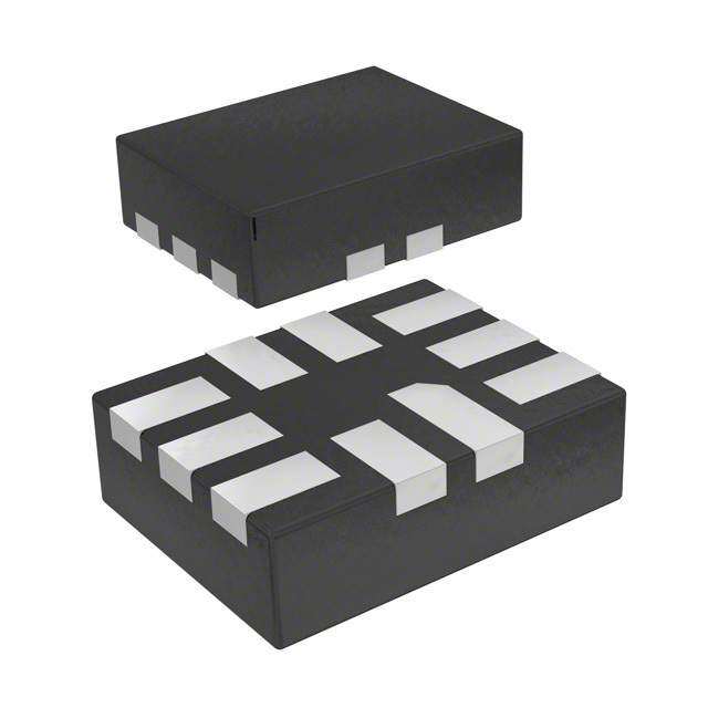
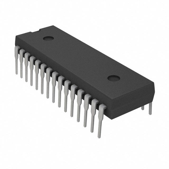
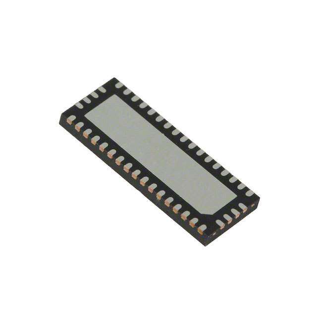
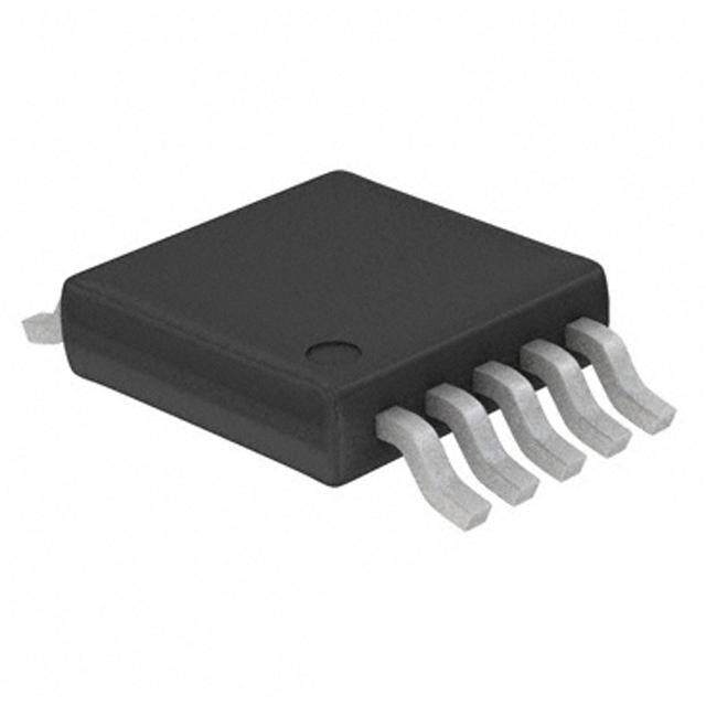
ICGOO在线商城 > 集成电路(IC) > 接口 - 模拟开关 - 专用 > TS3L110PWR
- 型号: TS3L110PWR
- 制造商: Texas Instruments
- 库位|库存: xxxx|xxxx
- 要求:
| 数量阶梯 | 香港交货 | 国内含税 |
| +xxxx | $xxxx | ¥xxxx |
查看当月历史价格
查看今年历史价格
TS3L110PWR产品简介:
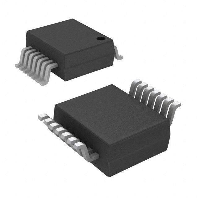
ICGOO电子元器件商城为您提供TS3L110PWR由Texas Instruments设计生产,在icgoo商城现货销售,并且可以通过原厂、代理商等渠道进行代购。 TS3L110PWR价格参考¥4.57-¥9.93。Texas InstrumentsTS3L110PWR封装/规格:接口 - 模拟开关 - 专用, 网络 开关 IC 4 通道 16-TSSOP。您可以下载TS3L110PWR参考资料、Datasheet数据手册功能说明书,资料中有TS3L110PWR 详细功能的应用电路图电压和使用方法及教程。
| 参数 | 数值 |
| 产品目录 | 集成电路 (IC)半导体 |
| 描述 | IC ETHERNET SWITCH QUAD 16TSSOP电源开关 IC - POE / LAN Quad SPDT Hi-BW- T Lan Sw Diff |
| 产品分类 | |
| 品牌 | Texas Instruments |
| 产品手册 | |
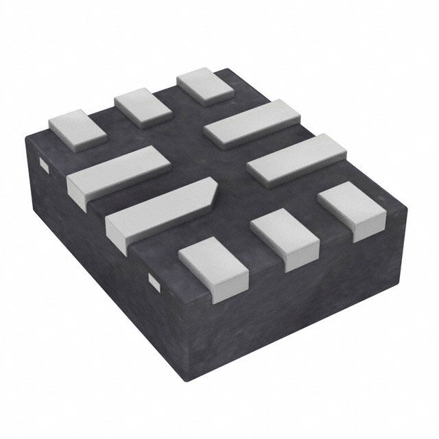
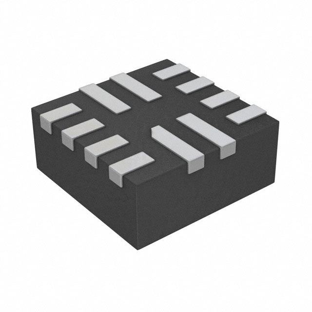
| 产品图片 |
|
| rohs | 符合RoHS无铅 / 符合限制有害物质指令(RoHS)规范要求 |
| 产品系列 | 开关 IC,电源开关 IC - POE / LAN,Texas Instruments TS3L110PWR3L |
| 数据手册 | |
| 产品型号 | TS3L110PWR |
| 产品目录页面 | |
| 产品种类 | 电源开关 IC - POE / LAN |
| 传播延迟时间 | 0.25 ns |
| 供应商器件封装 | 16-TSSOP |
| 其它名称 | 296-19015-1 |
| 制造商产品页 | http://www.ti.com/general/docs/suppproductinfo.tsp?distId=10&orderablePartNumber=TS3L110PWR |
| 功能 | 以太网开关 |
| 包装 | 剪切带 (CT) |
| 单位重量 | 62 mg |
| 商标 | Texas Instruments |
| 安装类型 | 表面贴装 |
| 安装风格 | SMD/SMT |
| 导通电阻 | 8 欧姆 |
| 导通电阻—最大值 | 8 Ohms |
| 封装 | Reel |
| 封装/外壳 | 16-TSSOP(0.173",4.40mm 宽) |
| 封装/箱体 | TSSOP-16 |
| 工作温度 | -40°C ~ 85°C |
| 工作电源电压 | 3.3 V |
| 工作电源电流 | 0.7 mA |
| 工厂包装数量 | 2000 |
| 开关数量 | Quad |
| 开关配置 | SPDT |
| 最大工作温度 | + 85 C |
| 最小工作温度 | - 40 C |
| 标准包装 | 1 |
| 电压-电源,单/双 (±) | 3 V ~ 3.6 V |
| 电压源 | 单电源 |
| 电流-电源 | 700µA |
| 电路 | 4 x SPDT |
| 空闲时间—最大值 | 5 ns |
| 系列 | TS3L110 |
| 运行时间—最大值 | 7 ns |



PDF Datasheet 数据手册内容提取
Product Order Technical Tools & Support & Folder Now Documents Software Community TS3L110 SCDS176B–SEPTEMBER2004–REVISEDOCTOBER2019 TS3L110 Quad SPDT High-Bandwidth 10/100 Base-T LAN Switch Differential 8-Channel to 4-Channel Multiplexer/Demultiplexer 1 Features To ensure the high-impedance state during power up or power down, E should be tied to V through a • Widebandwidth(BW=500MHztypical) CC 1 pullup resistor; the minimum value of the resistor is • Lowcrosstalk(XTALK =–30dBtypical) determined by the current-sinking capability of the • Bidirectionaldataflowwithnear-zeropropagation driver. delay DeviceInformation(1) • LowandflatON-stateresistance PARTNUMBER PACKAGE BODYSIZE(NOM) (r =4 Ωtypical,r =1 Ω) on on(flat) SOIC(D)16 9.90mmx3.91mm • SwitchingonDataI/OPorts(0to5V) SSOP(DBQ)16 4.90mmx3.90mm • V Operatingrangefrom3Vto3.6V CC TS3L110 TVSOP(DGV)16 3.60mmx4.40mm • I Supportspartialpower-down-modeoperation off TSSOP(PW)16 5.00mmx4.40mm • Dataandcontrolinputshaveundershootclamp VQFN(RGV)16 4.00mmx4.00mm diodes (1) For all available packages, see the orderable addendum at • Latch-upperformanceexceeds100mAPer theendofthedatasheet. JESD78,classII • ESDPerformancetestedperJESD22 LogicDiagram(PositiveLogic) – 2000-VHuman-bodymodel 4 2 (A114-B,classII) YA IA0 – 1000-VCharged-devicemodel(C101) 3 • Suitableforboth10Base-Tand100Base-T IA1 signaling 7 5 2 Applications YB IB0 • 10and100Base-Tsignalswitching 6 IB1 3 Description 9 11 The TS3L110 local area network (LAN) switch is a 4- YC IC0 bit 1-of-2 multiplexer/demultiplexer with a single switch-enable (E) input. When E is low, the switch is 10 enabled, and the I port is connected to the Y port. IC1 When E is high, the switch is disabled, and the high- impedance state exists between the I and Y ports. 12 14 The select (S) input controls the data path of the YD ID0 multiplexer/demultiplexer. 13 The TS3L110 device can be used to replace ID1 mechanical relays in LAN applications. This device has low and flat ON-state resistance (r ), wide on 1 bandwidth, and low crosstalk, making it suitable for S 10/100 Base-T and various other LAN applications. Control The TS3L110 device can be used to route signals 15 Logic E from a 10/100 Base-T Ethernet transceiver to the RJ- 45 LAN connectors in laptops or in docking stations. This device is designed for low channel-to-channel skewandlowcrosstalk. This device is fully specified for partial-power-down applications using I . The I feature ensures that off off damaging current does not backflow through the device when it is powered down. The device has isolationduringpoweroff. 1 An IMPORTANT NOTICE at the end of this data sheet addresses availability, warranty, changes, use in safety-critical applications, intellectualpropertymattersandotherimportantdisclaimers.PRODUCTIONDATA.
TS3L110 SCDS176B–SEPTEMBER2004–REVISEDOCTOBER2019 www.ti.com Table of Contents 1 Features.................................................................. 1 8.2 FunctionalBlockDiagram.......................................13 2 Applications........................................................... 1 8.3 FeatureDescription.................................................13 3 Description............................................................. 1 8.4 DeviceFunctionalModes........................................13 4 RevisionHistory..................................................... 2 9 ApplicationandImplementation........................ 14 9.1 ApplicationInformation............................................14 5 PinConfigurationandFunctions......................... 3 9.2 TypicalApplication .................................................14 6 Specifications......................................................... 4 10 PowerSupplyRecommendations..................... 15 6.1 AbsoluteMaximumRatings ....................................4 11 Layout................................................................... 16 6.2 ESDRatings..............................................................4 6.3 RecommendedOperatingConditions.....................4 11.1 LayoutGuidelines.................................................16 6.4 ThermalInformation..................................................5 11.2 LayoutExample....................................................17 6.5 ElectricalCharacteristics.........................................5 12 DeviceandDocumentationSupport................. 18 6.6 SwitchingCharacteristics.........................................6 12.1 ReceivingNotificationofDocumentationUpdates18 6.7 DynamicCharacteristics..........................................6 12.2 CommunityResources..........................................18 6.8 TypicalCharacteristics..............................................7 12.3 Trademarks...........................................................18 7 ParameterMeasurementInformation..................8 12.4 ElectrostaticDischargeCaution............................18 12.5 Glossary................................................................18 8 DetailedDescription............................................ 13 13 Mechanical,Packaging,andOrderable 8.1 Overview.................................................................13 Information........................................................... 18 4 Revision History NOTE:Pagenumbersforpreviousrevisionsmaydifferfrompagenumbersinthecurrentversion. ChangesfromRevisionA(May2019)toRevisionB Page • Changepin10toIC ,pin11toIC ,pin13toID ,andpin14toID inthePinConfigurationandFunctions.......................3 1 0 1 0 ChangesfromOriginal(September2004)toRevisionA Page • AddedDeviceInformationtable,ESDRatingstable,ThermalInformationtable,FeatureDescriptionsection,Device FunctionalModes,ApplicationandImplementationsection,PowerSupplyRecommendationssection,Layout section,DeviceandDocumentationSupportsection,andMechanical,Packaging,andOrderableInformationsection......1 2 SubmitDocumentationFeedback Copyright©2004–2019,TexasInstrumentsIncorporated ProductFolderLinks:TS3L110
TS3L110 www.ti.com SCDS176B–SEPTEMBER2004–REVISEDOCTOBER2019 5 Pin Configuration and Functions D,DBQ,DGV,orPWPackage SOIC,SSOP,TVSOP,TSSOP16Pins RGYPackage TopView VQFN16Pins TopView C S VC S 1 16 VCC IA0 2 15 E 1 6 IA1 3 14 ID0 1 IA0 2 15 E YA 4 13 ID1 IA1 3 14 ID0 IB0 5 12 YD YA 4 Thermal 13 ID1 IB1 6 11 IC0 Pad IB0 5 12 YD YB 7 10 IC1 IB1 6 11 IC0 GND 8 9 YC YB 7 10 IC1 Not to scale 8 9 Not to scale D C N Y G PinFunctions PIN DESCRIPTION NAME NO. S 1 Selectinput IA 2 DataI/Os 0 IA 3 DataI/Os 1 YA 4 DataI/Os IB 5 DataI/Os 0 IB 6 DataI/Os 1 YB 7 DataI/Os GND 8 Ground(0V)reference YC 9 DataI/Os IC 10 DataI/Os 1 IC 11 DataI/Os 0 YD 12 DataI/Os ID 13 DataI/Os 1 ID 14 DataI/Os 0 E 15 Enableinput Positivepowersupply.Thispinisthemostpositivepower-supplypotential.Forreliableoperation, V 16 CC connectadecouplingcapacitorrangingfrom0.1µFto10µFbetweenVDDandGND. Copyright©2004–2019,TexasInstrumentsIncorporated SubmitDocumentationFeedback 3 ProductFolderLinks:TS3L110
TS3L110 SCDS176B–SEPTEMBER2004–REVISEDOCTOBER2019 www.ti.com 6 Specifications 6.1 Absolute Maximum Ratings(1) overoperatingfree-airtemperaturerange(unlessotherwisenoted) MIN MAX UNIT V Supplyvoltagerange –0.5 4.6 V CC V Controlinputvoltagerange(2)(3) –0.5 7 V IN V SwitchI/Ovoltagerange(2)(3)(4) –0.5 7 V I/O I Controlinputclampcurrent V <0 –50 mA IK IN I I/Oportclampcurrent V <0 –50 mA I/OK I/O I ON-stateswitchcurrent(5) ±128 mA I/O ContinuouscurrentthroughV orGND ±100 mA CC Dpackage(6) 73 DBQpackage(6) 90 θ Packagethermalimpedance DGVpackage(6) 120 °C/W JA PWpackage(6) 108 RGYpackage(7) 39 T Storagetemperaturerange –65 150 °C stg (1) Stressesbeyondthoselistedunder"absolutemaximumratings"maycausepermanentdamagetothedevice.Thesearestressratings only,andfunctionaloperationofthedeviceattheseoranyotherconditionsbeyondthoseindicatedunder"recommendedoperating conditions"isnotimplied.Exposuretoabsolute-maximum-ratedconditionsforextendedperiodsmayaffectdevicereliability. (2) Allvoltagesarewithrespecttoground,unlessotherwisespecified. (3) Theinputandoutputvoltageratingsmaybeexceedediftheinputandoutputclamp-currentratingsareobserved. (4) V andV areusedtodenotespecificconditionsforV . I O I/O (5) I andI areusedtodenotespecificconditionsforI . I O I/O (6) ThepackagethermalimpedanceiscalculatedinaccordancewithJESD51-7. (7) ThepackagethermalimpedanceiscalculatedinaccordancewithJESD51-5. 6.2 ESD Ratings VALUE UNIT Human-bodymodel(HBM),perANSI/ESDA/JEDECJS-001(1) ±2000 V(ESD) Electrostaticdischarge Charged-devicemodel(CDM),perJEDECspecificationJESD22-C101 V orANSI/ESDA/JEDECJS-002(2) ±1000 (1) JEDECdocumentJEP155statesthat500-VHBMallowssafemanufacturingwithastandardESDcontrolprocess. (2) JEDECdocumentJEP157statesthat250-VCDMallowssafemanufacturingwithastandardESDcontrolprocess.e. 6.3 Recommended Operating Conditions(1) MIN MAX UNIT V Supplyvoltage 3 3.6 V CC V High-levelcontrolinputvoltage(E,S) 2 5.5 V IH V Low-levelcontrolinputvoltage(E,S) 0 0.8 V IL V Input/outputvoltage 0 5.5 V I/O T Operatingfree-airtemperature –40 85 °C A (1) AllunusedcontrolinputsofthedevicemustbeheldatV orGNDtoensureproperdeviceoperation.RefertotheTIapplicationreport, CC ImplicationsofSloworFloatingCMOSInputs,literaturenumberSCBA004. 4 SubmitDocumentationFeedback Copyright©2004–2019,TexasInstrumentsIncorporated ProductFolderLinks:TS3L110
TS3L110 www.ti.com SCDS176B–SEPTEMBER2004–REVISEDOCTOBER2019 6.4 Thermal Information TS3L110 THERMALMETRIC(1) D(SOIC) DBQ(SSOP) DGV(TVSOP) PW(TSSOP) RGV(VQFN) UNIT 16PINS 16PINS 16PINS 16PINS 16PINS RθJA Junction-to-ambientthermalresistance 92.0 114.5 139.3 111.5 50.8 °C/W RθJC(top) Junction-to-case(top)thermalresistance 52.3 60.5 57.4 42.0 48.1 °C/W RθJB Junction-to-boardthermalresistance 50.3 58.2 73.7 57.8 26.7 °C/W ψJT Junction-to-topcharacterizationparameter 17.3 15.3 7.2 4.2 2.1 °C/W ψJB Junction-to-boardcharacterizationparameter 50.0 57.6 73.0 57.2 26.5 °C/W RθJC(bot) Junction-to-case(bottom)thermalresistance - - - - 10.7 °C/W (1) Formoreinformationabouttraditionalandnewthermalmetrics,seetheSemiconductorandICpackagethermalmetricsapplication report. 6.5 Electrical Characteristics(1) overrecommendedoperatingfree-airtemperaturerange,V =3.3V±0.3V(unlessotherwisenoted) CC PARAMETER TESTCONDITIONS MIN TYP(2) MAX UNIT V E,S V =3.6V, I =–18mA –1.8 V IK CC IN I E,S V =3.6V, V =5.5V ±1 µA IH CC IN I E,S V =3.6V, V =GND ±1 µA IL CC IN I V =0, V =0to5.5V, V =0 1 µA off CC O I I V =3.6V, I =0, SwitchONorOFF 0.7 1.5 mA CC CC I/O C E,S f=1MHz, V =0 2.5 3.5 pF in IN V =0, f=1MHz, Iport I SwitchOFF 3.5 5 Outputsopen, C pF io(OFF) V =0, f=1MHz, Yport I SwitchOFF 5.5 7 Outputsopen, IorY f=1MHz, C V =0, SwitchON 10.5 13 pF io(ON) port I Outputsopen, r V =3V, 1.25V≤V ≤V , I =–10mAto–30mA 4 8 Ω on CC I CC O r (3) V =3V, V =1.25VandV , I =–10mAto–30mA 1 Ω on(flat) CC I CC O Δr (4) V =3V, 1.25V≤V ≤V , I =–10mAto–30mA 0.9 2 Ω on CC I CC O (1) V,V ,I,andI refertoI/Opins.V referstothecontrolinputs. I O I O IN (2) AlltypicalvaluesareatV =3.3V(unlessotherwisenoted),T =25°C. CC A (3) r isthedifferenceofr inagivenchannelatspecifiedvoltages. on(flat) on (4) Δr isthedifferenceofr inagivendevice. on on Copyright©2004–2019,TexasInstrumentsIncorporated SubmitDocumentationFeedback 5 ProductFolderLinks:TS3L110
TS3L110 SCDS176B–SEPTEMBER2004–REVISEDOCTOBER2019 www.ti.com 6.6 Switching Characteristics overrecommendedoperatingfree-airtemperaturerange,V =3.3V±0.3V,R =200Ω,C =10pF CC L L (unlessotherwisenoted)(seeFigure5andFigure6) PARAMETER FROM TO MIN TYP(1) MAX UNIT (INPUT) (OUTPUT) t (2) IorY YorI 0.25 ns pd t ,t EorS IorY 0.5 7 ns PZH PZL t ,t EorS IorY 0.5 5 ns PHZ PLZ t (3) IorY YorI 0.1 0.2 ns sk(p) (1) AlltypicalvaluesareatV =3.3V(unlessotherwisenoted),T =25°C. CC A (2) ThepropagationdelayisthecalculatedRCtimeconstantofthetypicalON-stateresistanceoftheswitchandthespecifiedload capacitancewhendrivenbyanidealvoltagesource(zerooutputimpedance). (3) Skewbetweenoppositetransitionsofthesameoutput|t –t |.Thisparameterisnotproductiontested. PHL PLH 6.7 Dynamic Characteristics overrecommendedoperatingfree-airtemperaturerange,V =3.3V±0.3V(unlessotherwisenoted) CC PARAMETER TESTCONDITIONS TYP(1) UNIT X R =100Ω, f=250MHz, SeeFigure7 –26 dB TALK L O R =100Ω, f=250MHz, SeeFigure8 –28 dB IRR L BW R =100Ω, SeeFigure6 500 MHz L (1) AlltypicalvaluesareatV =3.3V(unlessotherwisenoted),T =25°C. CC A 6 SubmitDocumentationFeedback Copyright©2004–2019,TexasInstrumentsIncorporated ProductFolderLinks:TS3L110
TS3L110 www.ti.com SCDS176B–SEPTEMBER2004–REVISEDOCTOBER2019 6.8 Typical Characteristics 0 0 20 120 Phase −1 −10 0 Phase 100 −2 Gain −20 −20 80 g) Gain (dB) −−43 −−3400 Phase (DeGain (dB) −40 Gain 60 Phase (Deg) −60 40 −5 −50 −6 −60 −80 20 −7 −70 −100 0 1 10 100 700 1 10 100 700 Frequency (MHz) Frequency (MHz) Phaseat627MHz,−36Deg Phaseat250MHz,88.2Deg Gain−3dBat627MHz Gain−28.5dBat250MHz Figure1.GainandPhasevsFrequency Figure2.OFFIsolationvsFrequency 0 180 5 20 −10 160 −20 140 4 16 −30 120 Gain (dB) −−−−76540000 PGhaaisne 186400000 Phase (Deg) Output Voltage (V) 23 VO 812 WState Resistance () −80 20 N- O −90 0 1 rON 4 1 10 100 700 Frequency (MHz) Phaseat250MHz,137.92Deg Gain−26dBat250MHZ 0 0 0 1 2 3 4 5 Input Voltage (V) Figure3.CrosstalkvsFrequency Figure4.OutputVoltageandON-StateResistancevsInput Voltage Copyright©2004–2019,TexasInstrumentsIncorporated SubmitDocumentationFeedback 7 ProductFolderLinks:TS3L110
TS3L110 SCDS176B–SEPTEMBER2004–REVISEDOCTOBER2019 www.ti.com 7 Parameter Measurement Information VCC Input Generator VIN 50 (W) VG1 50 (W) TEST CIRCUIT DUT 2 xVCC Input Generator S1 VI VO RL Open GND 50 (W) VG2 50 (W) CL RL (see NoteA) TEST VCC S1 RL VI CL VD tPLZ/tPZL 3.3 V±0.3 V 2 xVCC 200 (W) GND 10 pF 0.3 V tPHZ/tPZH 3.3 V±0.3 V GND 200(W) VCC 10 pF 0.3 V Output Control 2.5 V (VIN) 1.25 V 1.25 V Output 0 V Waveform 1 S1 at 2 VCCtPZL tPLZ (see Note B) VOH VCC/2 VOL+ 0.3 V VOL tPZH tPHZ Output Waveform 2 VOH−0.3 V VOH S1 at GND VCC/2 (see Note B) VOL VOLTAGE WAVEFORMS ENABLEAND DISABLE TIMES A. C includesprobeandjigcapacitance. L B. Waveform 1 is for an output with internal conditions such that the output is low. Waveform 2 is for an output with internalconditionssuchthattheoutputishigh,exceptwhendisabledbytheoutputcontrol. C. Allinputpulsesaresuppliedbygeneratorshavingthefollowingcharacteristics:PRR≤10MHz,Z =50Ω,t ≤2.5ns, O r t ≤2.5ns. f D. Theoutputsaremeasuredoneatatime,withonetransitionpermeasurement. E. t andt arethesameast . PLZ PHZ dis F. t andt arethesameast . PLZ PHH en Figure5. TestCircuitandVoltageWaveforms 8 SubmitDocumentationFeedback Copyright©2004–2019,TexasInstrumentsIncorporated ProductFolderLinks:TS3L110
TS3L110 www.ti.com SCDS176B–SEPTEMBER2004–REVISEDOCTOBER2019 Parameter Measurement Information (continued) VCC Input Generator VIN 50W VG1 50W TEST CIRCUIT DUT 2 xVCC Input Generator S1 VI VO RL Open 50W GND VG2 50W CL RL (see NoteA) VIN TEST VCC S1 RL (see Note B) CL tsk(p) 3.3 V±0.3 V GND 200W VCCorGND 10 pF 3.5 V Data Input 2.5 V 1.5 V tPLH tPHL VOH Data Output (VOH+ VOL)/2 VOL tsk(p)= tPHL−tPLH VOLTAGE WAVEFORMS PULSE SKEW [tsk(p)] A. C includesprobeandjigcapacitance. L B. SwitchisONduringthemeasurementoft ,thatis,voltageatE=0andS=V orGND. sk(p) CC Figure6. TestCircuitandVoltageWaveforms Copyright©2004–2019,TexasInstrumentsIncorporated SubmitDocumentationFeedback 9 ProductFolderLinks:TS3L110
TS3L110 SCDS176B–SEPTEMBER2004–REVISEDOCTOBER2019 www.ti.com Parameter Measurement Information (continued) EXT TRIGGER BIAS VBIAS NetworkAnalyzer (HP8753ES) P1 P2 VCC YA IA0 CL= 10 pF RL= 100W (see NoteA) S DUT VS E VE A. C includesprobeandjigcapacitance. L Figure7. TestCircuitforFrequencyResponse(BW) Frequency response is measured at the output of the ON channel. For example, when V = 0, V = 0, and YA is S E theinput,theoutputismeasuredatIA .AllunusedanalogI/Oportsareleftopen. 0 HP8753ESSetup • Average=4 • RBW=3kHz • V =0.35V BIAS • ST=2s • P1=0dBM 10 SubmitDocumentationFeedback Copyright©2004–2019,TexasInstrumentsIncorporated ProductFolderLinks:TS3L110
TS3L110 www.ti.com SCDS176B–SEPTEMBER2004–REVISEDOCTOBER2019 Parameter Measurement Information (continued) EXT TRIGGER BIAS VBIAS NetworkAnalyzer (HP8753ES) P1 P2 VCC YA IA0 S RL= 100W CL= 10 pF 50W (see NoteA) (see Note B) VS E DUT VE YB IB0 RL= 100W CL= 10 pF (see NoteA) A. C includesprobeandjigcapacitance. L B. A50-Ωterminationresistorisneededtomatchtheloadingofthenetworkanalyzer Figure8. TestCircuitforCrosstalk(X ) TALK Crosstalk is measured at the output of the nonadjacent ON channel. For example, when V = 0, V = 0, and YA S E is the input, the output is measured at IB . All unused analog input (Y) ports are connected to GND, and output 0 (I)portsareconnectedtoGNDthrough50-Ω pulldownresistors. HP8753ESSetup • Average=4 • RBW=3kHz • V =0.35V BIAS • ST=2s • P1=0dBM Copyright©2004–2019,TexasInstrumentsIncorporated SubmitDocumentationFeedback 11 ProductFolderLinks:TS3L110
TS3L110 SCDS176B–SEPTEMBER2004–REVISEDOCTOBER2019 www.ti.com Parameter Measurement Information (continued) EXT TRIGGER BIAS VBIAS NetworkAnalyzer (HP8753ES) P1 P2 VCC YA IA0 RL= 100W CL= 10 pF (see NoteA) S DUT VS IA1 E RL= 100W CL= 10 pF 50W VE (see NoteA) (see Note B) A. C includesprobeandjigcapacitance. L B. A50-Ωterminationresistorisneededtomatchtheloadingofthenetworkanalyzer Figure9. TestCircuitforOFFIsolation(O ) IRR OFF isolation is measured at the output of the OFF channel. For example, when V = V , V = 0, and YA is the S CC E input, the output is measured at IA . All unused analog input (Y) ports are left open, and output (I) ports are 0 connectedtoGNDthrough50-Ω pulldownresistors. HP8753FSSetup • Average=4 • RBW=3kHz • V =0.35V BIAS • ST=2s • P1=0dBM 12 SubmitDocumentationFeedback Copyright©2004–2019,TexasInstrumentsIncorporated ProductFolderLinks:TS3L110
TS3L110 www.ti.com SCDS176B–SEPTEMBER2004–REVISEDOCTOBER2019 8 Detailed Description 8.1 Overview The TI TS3L110 LAN switch is a 4-bit 1-of-2 multiplexer/demultiplexer with a single switch-enable (E) input. When E is low, the switch is enabled, and the I port is connected to the Y port. When E is high, the switch is disabled, and the high-impedance state exists between the I and Y ports. The select (S) input controls the data pathofthemultiplexer/demultiplexer. 8.2 Functional Block Diagram 4 2 YA IA0 3 IA1 7 5 YB IB0 6 IB1 9 11 YC IC0 10 IC1 12 14 YD ID0 13 ID1 1 S Control 15 Logic E 8.3 Feature Description I supportsPartial-Power-DownModeOperation. off TheTS3L110deviceensuresthesignalpathishighimpedancestatewhenV =0V. CC 8.4 Device Functional Modes The TS3L110 supports a power down mode which reduces the current consumption of the device and places all thesignalpathsinahighimpedancestate.ToplacetheTS3L100inpowerdownmode,setthe Epinwithalogic highvoltageasseeninTable1. Table1.FunctionTable INPUTS INPUT/OUTPUT FUNCTION E S YX L L IX YX=IX 0 0 L H IX YX=IX 1 1 H X Z Disconnect Copyright©2004–2019,TexasInstrumentsIncorporated SubmitDocumentationFeedback 13 ProductFolderLinks:TS3L110
TS3L110 SCDS176B–SEPTEMBER2004–REVISEDOCTOBER2019 www.ti.com 9 Application and Implementation NOTE Information in the following applications sections is not part of the TI component specification, and TI does not warrant its accuracy or completeness. TI’s customers are responsible for determining suitability of components for their purposes. Customers should validateandtesttheirdesignimplementationtoconfirmsystemfunctionality. 9.1 Application Information There are many Local Area Network (LAN) applications in which the ethernet hubs or controllers have a limited number of I/Os or need to route signals from a single ethernet PHY to multiple ethernet jacks. The TS3L110 solution can effectively expand the limited I/Os by switching between multiple Ethernet jacks to interface them to asingleEthernetPHY. 9.2 Typical Application V CC Processor TS3L110 4 4 EPHthYernet YX IX RJ45 Port 1 4 IX RJ45 Port 2 S GPIO E GPIO GND Figure10. TypicalApplicationSchematic 9.2.1 DesignRequirements Ensure that all of the signals passing through the switch are within the recommended operating ranges. To ensureproperperformance,seeRecommendedOperatingConditions. 9.2.2 DetailedDesignProcedure The TS3L110 can be properly operated without any external components. TI recommends that the digital control pins S and E be pulled up to VCC or down to GND to avoid undesired switch positions that could result from the floatingpin.Connecttheexposedthermalpadtoground. 14 SubmitDocumentationFeedback Copyright©2004–2019,TexasInstrumentsIncorporated ProductFolderLinks:TS3L110
TS3L110 www.ti.com SCDS176B–SEPTEMBER2004–REVISEDOCTOBER2019 Typical Application (continued) 9.2.3 ApplicationCurves 0 0 Phase −1 −10 −2 Gain −20 g) e n (dB) −3 −30 hase (D Gai −4 −40 P −5 −50 −6 −60 −7 −70 1 10 100 700 Frequency (MHz) Phaseat627MHz, −36Deg Gain−3dBat627MHz Figure11.GainandPhasevsFrequency 10 Power Supply Recommendations PowertothedeviceissuppliedthroughtheVCCpins.TIrecommendsplacingabypasscapacitorasclosetothe supplypin(VCC)aspossibletohelpsmoothoutlowerfrequencynoisetoprovidebetterloadregulationacross thefrequencyspectrum. Copyright©2004–2019,TexasInstrumentsIncorporated SubmitDocumentationFeedback 15 ProductFolderLinks:TS3L110
TS3L110 SCDS176B–SEPTEMBER2004–REVISEDOCTOBER2019 www.ti.com 11 Layout 11.1 Layout Guidelines • TIrecommendskeepingthehigh-speedsignalsasshortaspossible. • Each via introduces discontinuities in the transmission line of the signal and increases the chance of picking up interference from the other layers of the board. Be careful when designing test points on twisted pair lines; through-holepinsarenotrecommended. • When it becomes necessary to turn 90°, use two 45° turns or an arc instead of making a single 90° turn. This reducesreflectionsonthesignaltracesbyminimizingimpedancediscontinuities. • Do not route traces under or near crystals, oscillators, clock signal generators, switching regulators, mounting holes,magneticdevicesorICsthatuseorduplicateclocksignals. • Avoid stubs on the high-speed signals because they cause signal reflections. If a stub is unavoidable, then thestubmustbelessthan200mm. • Route all high-speed signal traces over continuous GND planes, with no interruptions. Avoid crossing over anti-etch,commonlyfoundwithplanesplits. • Due to high-frequency signals, a printed-circuit board with at least four layers is recommended; two signal layersseparatedbyagroundandpowerlayerasshowninFigure12. • The majority of signal traces must run on a single layer, preferably Signal 1. Immediately next to this layer should be the GND plane, which is solid with no cuts. Avoid running signal traces across a split in the ground or power plane. When running across split planes is unavoidable, sufficient decoupling must be used. MinimizingthenumberofsignalviasreducesEMIbyreducinginductanceathighfrequencies. Signal 1 GND Plane Power Plane Signal 2 Figure12. Four-LayerBoardStackup 16 SubmitDocumentationFeedback Copyright©2004–2019,TexasInstrumentsIncorporated ProductFolderLinks:TS3L110
TS3L110 www.ti.com SCDS176B–SEPTEMBER2004–REVISEDOCTOBER2019 11.2 Layout Example V DD To To To System System System 0603 42 41 40 39 To System 1 38 To System To System 2 37 To System To System 3 36 To System To System 4 35 To System To System 5 34 To System To System 6 33 To System To System 7 32 To System 8 31 Exposed Center To System 9 Pad 30 (GND) To System To System 10 29 To System To System 11 28 To System To System 12 27 To System To System 13 26 To System 14 25 To System To System 15 24 To System To System 16 23 To System To System 17 22 18 19 20 21 To To To System System System Figure13. LayoutExample Copyright©2004–2019,TexasInstrumentsIncorporated SubmitDocumentationFeedback 17 ProductFolderLinks:TS3L110
TS3L110 SCDS176B–SEPTEMBER2004–REVISEDOCTOBER2019 www.ti.com 12 Device and Documentation Support 12.1 Receiving Notification of Documentation Updates To receive notification of documentation updates, navigate to the device product folder on ti.com. In the upper right corner, click on Alert me to register and receive a weekly digest of any product information that has changed.Forchangedetails,reviewtherevisionhistoryincludedinanyreviseddocument. 12.2 Community Resources TI E2E™ support forums are an engineer's go-to source for fast, verified answers and design help — straight fromtheexperts.Searchexistinganswersoraskyourownquestiontogetthequickdesignhelpyouneed. Linked content is provided "AS IS" by the respective contributors. They do not constitute TI specifications and do notnecessarilyreflectTI'sviews;seeTI'sTermsofUse. 12.3 Trademarks E2EisatrademarkofTexasInstruments. Allothertrademarksarethepropertyoftheirrespectiveowners. 12.4 Electrostatic Discharge Caution This integrated circuit can be damaged by ESD. Texas Instruments recommends that all integrated circuits be handled with appropriateprecautions.Failuretoobserveproperhandlingandinstallationprocedurescancausedamage. ESDdamagecanrangefromsubtleperformancedegradationtocompletedevicefailure.Precisionintegratedcircuitsmaybemore susceptibletodamagebecauseverysmallparametricchangescouldcausethedevicenottomeetitspublishedspecifications. 12.5 Glossary SLYZ022—TIGlossary. Thisglossarylistsandexplainsterms,acronyms,anddefinitions. 13 Mechanical, Packaging, and Orderable Information The following pages include mechanical, packaging, and orderable information. This information is the most current data available for the designated devices. This data is subject to change without notice and revision of thisdocument.Forbrowser-basedversionsofthisdatasheet,refertotheleft-handnavigation. 18 SubmitDocumentationFeedback Copyright©2004–2019,TexasInstrumentsIncorporated ProductFolderLinks:TS3L110
PACKAGE OPTION ADDENDUM www.ti.com 6-Feb-2020 PACKAGING INFORMATION Orderable Device Status Package Type Package Pins Package Eco Plan Lead/Ball Finish MSL Peak Temp Op Temp (°C) Device Marking Samples (1) Drawing Qty (2) (6) (3) (4/5) TS3L110D ACTIVE SOIC D 16 40 Green (RoHS NIPDAU Level-1-260C-UNLIM -40 to 85 TS3L110 & no Sb/Br) TS3L110DBQR ACTIVE SSOP DBQ 16 2500 Green (RoHS NIPDAU Level-2-260C-1 YEAR -40 to 85 TK110 & no Sb/Br) TS3L110DBQRG4 ACTIVE SSOP DBQ 16 2500 Green (RoHS NIPDAU Level-2-260C-1 YEAR -40 to 85 TK110 & no Sb/Br) TS3L110DE4 ACTIVE SOIC D 16 40 Green (RoHS NIPDAU Level-1-260C-UNLIM -40 to 85 TS3L110 & no Sb/Br) TS3L110DG4 ACTIVE SOIC D 16 40 Green (RoHS NIPDAU Level-1-260C-UNLIM -40 to 85 TS3L110 & no Sb/Br) TS3L110DGVR ACTIVE TVSOP DGV 16 2000 Green (RoHS NIPDAU Level-1-260C-UNLIM -40 to 85 TK110 & no Sb/Br) TS3L110DR ACTIVE SOIC D 16 2500 Green (RoHS NIPDAU Level-1-260C-UNLIM -40 to 85 TS3L110 & no Sb/Br) TS3L110PW ACTIVE TSSOP PW 16 90 Green (RoHS NIPDAU Level-1-260C-UNLIM -40 to 85 TK110 & no Sb/Br) TS3L110PWR ACTIVE TSSOP PW 16 2000 Green (RoHS NIPDAU Level-1-260C-UNLIM -40 to 85 TK110 & no Sb/Br) TS3L110PWRE4 ACTIVE TSSOP PW 16 2000 Green (RoHS NIPDAU Level-1-260C-UNLIM -40 to 85 TK110 & no Sb/Br) TS3L110PWRG4 ACTIVE TSSOP PW 16 2000 Green (RoHS NIPDAU Level-1-260C-UNLIM -40 to 85 TK110 & no Sb/Br) TS3L110RGYR ACTIVE VQFN RGY 16 3000 Green (RoHS NIPDAU Level-2-260C-1 YEAR -40 to 85 TK110 & no Sb/Br) (1) The marketing status values are defined as follows: ACTIVE: Product device recommended for new designs. LIFEBUY: TI has announced that the device will be discontinued, and a lifetime-buy period is in effect. NRND: Not recommended for new designs. Device is in production to support existing customers, but TI does not recommend using this part in a new design. PREVIEW: Device has been announced but is not in production. Samples may or may not be available. OBSOLETE: TI has discontinued the production of the device. (2) RoHS: TI defines "RoHS" to mean semiconductor products that are compliant with the current EU RoHS requirements for all 10 RoHS substances, including the requirement that RoHS substance do not exceed 0.1% by weight in homogeneous materials. Where designed to be soldered at high temperatures, "RoHS" products are suitable for use in specified lead-free processes. TI may reference these types of products as "Pb-Free". RoHS Exempt: TI defines "RoHS Exempt" to mean products that contain lead but are compliant with EU RoHS pursuant to a specific EU RoHS exemption. Addendum-Page 1
PACKAGE OPTION ADDENDUM www.ti.com 6-Feb-2020 Green: TI defines "Green" to mean the content of Chlorine (Cl) and Bromine (Br) based flame retardants meet JS709B low halogen requirements of <=1000ppm threshold. Antimony trioxide based flame retardants must also meet the <=1000ppm threshold requirement. (3) MSL, Peak Temp. - The Moisture Sensitivity Level rating according to the JEDEC industry standard classifications, and peak solder temperature. (4) There may be additional marking, which relates to the logo, the lot trace code information, or the environmental category on the device. (5) Multiple Device Markings will be inside parentheses. Only one Device Marking contained in parentheses and separated by a "~" will appear on a device. If a line is indented then it is a continuation of the previous line and the two combined represent the entire Device Marking for that device. (6) Lead/Ball Finish - Orderable Devices may have multiple material finish options. Finish options are separated by a vertical ruled line. Lead/Ball Finish values may wrap to two lines if the finish value exceeds the maximum column width. Important Information and Disclaimer:The information provided on this page represents TI's knowledge and belief as of the date that it is provided. TI bases its knowledge and belief on information provided by third parties, and makes no representation or warranty as to the accuracy of such information. Efforts are underway to better integrate information from third parties. TI has taken and continues to take reasonable steps to provide representative and accurate information but may not have conducted destructive testing or chemical analysis on incoming materials and chemicals. TI and TI suppliers consider certain information to be proprietary, and thus CAS numbers and other limited information may not be available for release. In no event shall TI's liability arising out of such information exceed the total purchase price of the TI part(s) at issue in this document sold by TI to Customer on an annual basis. Addendum-Page 2
PACKAGE MATERIALS INFORMATION www.ti.com 16-Oct-2019 TAPE AND REEL INFORMATION *Alldimensionsarenominal Device Package Package Pins SPQ Reel Reel A0 B0 K0 P1 W Pin1 Type Drawing Diameter Width (mm) (mm) (mm) (mm) (mm) Quadrant (mm) W1(mm) TS3L110DBQR SSOP DBQ 16 2500 330.0 12.5 6.4 5.2 2.1 8.0 12.0 Q1 TS3L110DGVR TVSOP DGV 16 2000 330.0 12.4 6.8 4.0 1.6 8.0 12.0 Q1 TS3L110DR SOIC D 16 2500 330.0 16.4 6.5 10.3 2.1 8.0 16.0 Q1 TS3L110PWR TSSOP PW 16 2000 330.0 12.4 6.9 5.6 1.6 8.0 12.0 Q1 TS3L110RGYR VQFN RGY 16 3000 330.0 12.4 3.8 4.3 1.5 8.0 12.0 Q1 PackMaterials-Page1
PACKAGE MATERIALS INFORMATION www.ti.com 16-Oct-2019 *Alldimensionsarenominal Device PackageType PackageDrawing Pins SPQ Length(mm) Width(mm) Height(mm) TS3L110DBQR SSOP DBQ 16 2500 340.5 338.1 20.6 TS3L110DGVR TVSOP DGV 16 2000 367.0 367.0 35.0 TS3L110DR SOIC D 16 2500 333.2 345.9 28.6 TS3L110PWR TSSOP PW 16 2000 367.0 367.0 35.0 TS3L110RGYR VQFN RGY 16 3000 367.0 367.0 35.0 PackMaterials-Page2
None
None
PACKAGE OUTLINE PW0016A TSSOP - 1.2 mm max height SCALE 2.500 SMALL OUTLINE PACKAGE SEATING PLANE C 6.6 TYP 6.2 A 0.1 C PIN 1 INDEX AREA 14X 0.65 16 1 2X 5.1 4.55 4.9 NOTE 3 8 9 0.30 B 4.5 16X 0.19 1.2 MAX 4.3 0.1 C A B NOTE 4 (0.15) TYP SEE DETAIL A 0.25 GAGE PLANE 0.15 0.05 0.75 0.50 0 -8 DETA 20AIL A TYPICAL 4220204/A 02/2017 NOTES: 1. All linear dimensions are in millimeters. Any dimensions in parenthesis are for reference only. Dimensioning and tolerancing per ASME Y14.5M. 2. This drawing is subject to change without notice. 3. This dimension does not include mold flash, protrusions, or gate burrs. Mold flash, protrusions, or gate burrs shall not exceed 0.15 mm per side. 4. This dimension does not include interlead flash. Interlead flash shall not exceed 0.25 mm per side. 5. Reference JEDEC registration MO-153. www.ti.com
EXAMPLE BOARD LAYOUT PW0016A TSSOP - 1.2 mm max height SMALL OUTLINE PACKAGE 16X (1.5) SYMM (R0.05) TYP 1 16X (0.45) 16 SYMM 14X (0.65) 8 9 (5.8) LAND PATTERN EXAMPLE EXPOSED METAL SHOWN SCALE: 10X SOLDER MASK METAL UNDER SOLDER MASK OPENING METAL SOLDER MASK OPENING EXPOSED METAL EXPOSED METAL 0.05 MAX 0.05 MIN ALL AROUND ALL AROUND NON-SOLDER MASK SOLDER MASK DEFINED DEFINED (PREFERRED) SOLDE15.000R MASK DETAILS 4220204/A 02/2017 NOTES: (continued) 6. Publication IPC-7351 may have alternate designs. 7. Solder mask tolerances between and around signal pads can vary based on board fabrication site. www.ti.com
EXAMPLE STENCIL DESIGN PW0016A TSSOP - 1.2 mm max height SMALL OUTLINE PACKAGE 16X (1.5) SYMM (R0.05) TYP 1 16X (0.45) 16 SYMM 14X (0.65) 8 9 (5.8) SOLDER PASTE EXAMPLE BASED ON 0.125 mm THICK STENCIL SCALE: 10X 4220204/A 02/2017 NOTES: (continued) 8. Laser cutting apertures with trapezoidal walls and rounded corners may offer better paste release. IPC-7525 may have alternate design recommendations. 9. Board assembly site may have different recommendations for stencil design. www.ti.com
MECHANICAL DATA MPDS006C – FEBRUARY 1996 – REVISED AUGUST 2000 DGV (R-PDSO-G**) PLASTIC SMALL-OUTLINE 24 PINS SHOWN 0,23 0,40 0,07 M 0,13 24 13 0,16 NOM 4,50 6,60 4,30 6,20 Gage Plane 0,25 0°–(cid:1)8° 0,75 1 12 0,50 A Seating Plane 0,15 1,20 MAX 0,08 0,05 PINS ** 14 16 20 24 38 48 56 DIM A MAX 3,70 3,70 5,10 5,10 7,90 9,80 11,40 A MIN 3,50 3,50 4,90 4,90 7,70 9,60 11,20 4073251/E 08/00 NOTES: A. All linear dimensions are in millimeters. B. This drawing is subject to change without notice. C. Body dimensions do not include mold flash or protrusion, not to exceed 0,15 per side. D. Falls within JEDEC: 24/48 Pins – MO-153 14/16/20/56 Pins – MO-194 • POST OFFICE BOX 655303 DALLAS, TEXAS 75265
None
PACKAGE OUTLINE DBQ0016A SSOP - 1.75 mm max height SCALE 2.800 SHRINK SMALL-OUTLINE PACKAGE C SEATING PLANE .228-.244 TYP [5.80-6.19] .004 [0.1] C A PIN 1 ID AREA 14X .0250 [0.635] 16 1 2X .189-.197 .175 [4.81-5.00] [4.45] NOTE 3 8 9 16X .008-.012 B .150-.157 [0.21-0.30] .069 MAX [3.81-3.98] [1.75] NOTE 4 .007 [0.17] C A B .005-.010 TYP [0.13-0.25] SEE DETAIL A .010 [0.25] GAGE PLANE .004-.010 0 - 8 [0.11-0.25] .016-.035 [0.41-0.88] DETAIL A (.041 ) TYPICAL [1.04] 4214846/A 03/2014 NOTES: 1. Linear dimensions are in inches [millimeters]. Dimensions in parenthesis are for reference only. Controlling dimensions are in inches. Dimensioning and tolerancing per ASME Y14.5M. 2. This drawing is subject to change without notice. 3. This dimension does not include mold flash, protrusions, or gate burrs. Mold flash, protrusions, or gate burrs shall not exceed .006 inch, per side. 4. This dimension does not include interlead flash. 5. Reference JEDEC registration MO-137, variation AB. www.ti.com
EXAMPLE BOARD LAYOUT DBQ0016A SSOP - 1.75 mm max height SHRINK SMALL-OUTLINE PACKAGE 16X (.063) [1.6] SYMM SEE DETAILS 1 16 16X (.016 ) [0.41] 14X (.0250 ) [0.635] 8 9 (.213) [5.4] LAND PATTERN EXAMPLE SCALE:8X SOLDER MASK SOLDER MASK METAL OPENING OPENING METAL .002 MAX .002 MIN [0.05] [0.05] ALL AROUND ALL AROUND NON SOLDER MASK SOLDER MASK DEFINED DEFINED SOLDER MASK DETAILS 4214846/A 03/2014 NOTES: (continued) 6. Publication IPC-7351 may have alternate designs. 7. Solder mask tolerances between and around signal pads can vary based on board fabrication site. www.ti.com
EXAMPLE STENCIL DESIGN DBQ0016A SSOP - 1.75 mm max height SHRINK SMALL-OUTLINE PACKAGE 16X (.063) [1.6] SYMM 1 16 16X (.016 ) [0.41] SYMM 14X (.0250 ) [0.635] 8 9 (.213) [5.4] SOLDER PASTE EXAMPLE BASED ON .005 INCH [0.127 MM] THICK STENCIL SCALE:8X 4214846/A 03/2014 NOTES: (continued) 8. Laser cutting apertures with trapezoidal walls and rounded corners may offer better paste release. IPC-7525 may have alternate design recommendations. 9. Board assembly site may have different recommendations for stencil design. www.ti.com
None
None
None
IMPORTANTNOTICEANDDISCLAIMER TI PROVIDES TECHNICAL AND RELIABILITY DATA (INCLUDING DATASHEETS), DESIGN RESOURCES (INCLUDING REFERENCE DESIGNS), APPLICATION OR OTHER DESIGN ADVICE, WEB TOOLS, SAFETY INFORMATION, AND OTHER RESOURCES “AS IS” AND WITH ALL FAULTS, AND DISCLAIMS ALL WARRANTIES, EXPRESS AND IMPLIED, INCLUDING WITHOUT LIMITATION ANY IMPLIED WARRANTIES OF MERCHANTABILITY, FITNESS FOR A PARTICULAR PURPOSE OR NON-INFRINGEMENT OF THIRD PARTY INTELLECTUAL PROPERTY RIGHTS. These resources are intended for skilled developers designing with TI products. You are solely responsible for (1) selecting the appropriate TI products for your application, (2) designing, validating and testing your application, and (3) ensuring your application meets applicable standards, and any other safety, security, or other requirements. These resources are subject to change without notice. TI grants you permission to use these resources only for development of an application that uses the TI products described in the resource. Other reproduction and display of these resources is prohibited. No license is granted to any other TI intellectual property right or to any third party intellectual property right. TI disclaims responsibility for, and you will fully indemnify TI and its representatives against, any claims, damages, costs, losses, and liabilities arising out of your use of these resources. TI’s products are provided subject to TI’s Terms of Sale (www.ti.com/legal/termsofsale.html) or other applicable terms available either on ti.com or provided in conjunction with such TI products. TI’s provision of these resources does not expand or otherwise alter TI’s applicable warranties or warranty disclaimers for TI products. Mailing Address: Texas Instruments, Post Office Box 655303, Dallas, Texas 75265 Copyright © 2020, Texas Instruments Incorporated

 Datasheet下载


