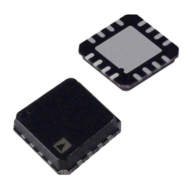
ICGOO在线商城 > 集成电路(IC) > 接口 - 模拟开关,多路复用器,多路分解器 > TS3A4751RGYR
- 型号: TS3A4751RGYR
- 制造商: Texas Instruments
- 库位|库存: xxxx|xxxx
- 要求:
| 数量阶梯 | 香港交货 | 国内含税 |
| +xxxx | $xxxx | ¥xxxx |
查看当月历史价格
查看今年历史价格
TS3A4751RGYR产品简介:
ICGOO电子元器件商城为您提供TS3A4751RGYR由Texas Instruments设计生产,在icgoo商城现货销售,并且可以通过原厂、代理商等渠道进行代购。 TS3A4751RGYR价格参考。Texas InstrumentsTS3A4751RGYR封装/规格:接口 - 模拟开关,多路复用器,多路分解器, 4 Circuit IC Switch 1:1 900 mOhm 14-VQFN (3.5x3.5)。您可以下载TS3A4751RGYR参考资料、Datasheet数据手册功能说明书,资料中有TS3A4751RGYR 详细功能的应用电路图电压和使用方法及教程。
| 参数 | 数值 |
| 产品目录 | 集成电路 (IC)半导体 |
| 描述 | IC SWITCH QUAD SPST 14QFN模拟开关 IC Quad SPST 0.9-Ohm Switch |
| 产品分类 | |
| 品牌 | Texas Instruments |
| 产品手册 | |
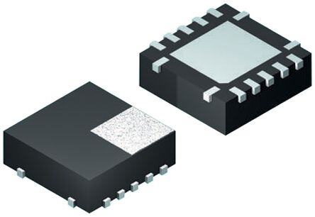
| 产品图片 |
|
| rohs | 符合RoHS无铅 / 符合限制有害物质指令(RoHS)规范要求 |
| 产品系列 | 开关 IC,模拟开关 IC,Texas Instruments TS3A4751RGYR- |
| 数据手册 | |
| 产品型号 | TS3A4751RGYR |
| 产品培训模块 | http://www.digikey.cn/PTM/IndividualPTM.page?site=cn&lang=zhs&ptm=26070 |
| 产品目录页面 | |
| 产品种类 | 模拟开关 IC |
| 供应商器件封装 | 14-VQFN (3.5x3.5) |
| 其它名称 | 296-24477-6 |
| 制造商产品页 | http://www.ti.com/general/docs/suppproductinfo.tsp?distId=10&orderablePartNumber=TS3A4751RGYR |
| 功能 | |
| 包装 | Digi-Reel® |
| 单位重量 | 32.200 mg |
| 商标 | Texas Instruments |
| 安装类型 | 表面贴装 |
| 安装风格 | SMD/SMT |
| 导通电阻 | 900 毫欧 |
| 导通电阻—最大值 | 0.9 Ohms |
| 封装 | Reel |
| 封装/外壳 | 14-VFQFN 裸露焊盘 |
| 封装/箱体 | VQFN-14 |
| 工作温度 | -40°C ~ 85°C |
| 工作电源电压 | 1.65 V to 3.6 V |
| 工厂包装数量 | 3000 |
| 开关数量 | 4 |
| 开关配置 | SPST |
| 最大工作温度 | + 85 C |
| 最小工作温度 | - 40 C |
| 标准包装 | 1 |
| 电压-电源,单/双 (±) | 1.6 V ~ 3.6 V |
| 电压源 | 单电源 |
| 电流-电源 | - |
| 电源电压-最大 | 3.6 V |
| 电源电压-最小 | 1.65 V |
| 电源电流 | 0.075 uA |
| 电源电流—最大值 | 0.75 uA |
| 电路 | 4 x SPST - NO |
| 空闲时间—最大值 | 9 ns |
| 系列 | TS3A4751 |
| 运行时间—最大值 | 15 ns |
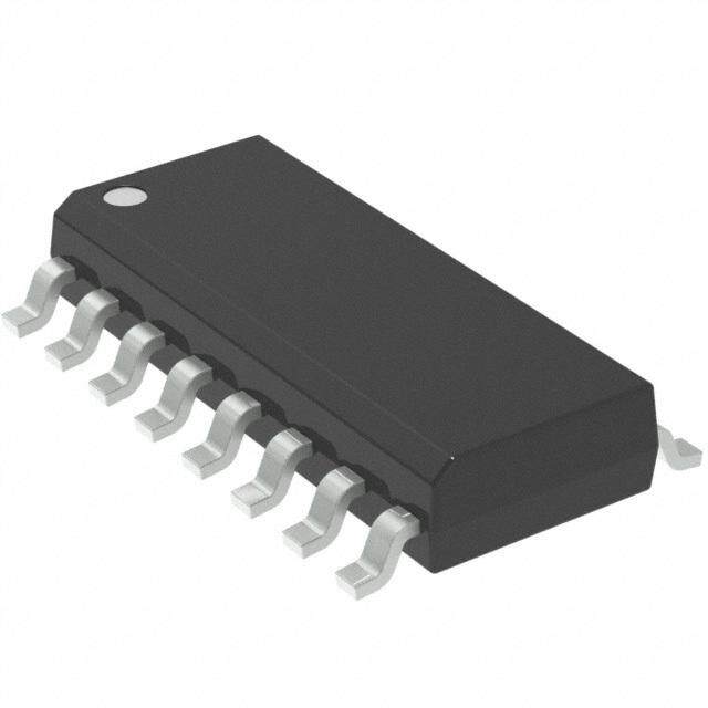


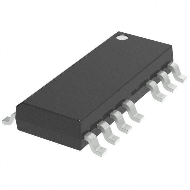

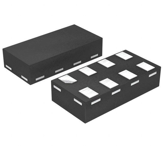

PDF Datasheet 数据手册内容提取
Product Order Technical Tools & Support & Folder Now Documents Software Community TS3A4751 SCDS227F–JULY2006–REVISEDMARCH2015 TS3A4751 0.9-Ω Low-voltage, single-supply, 4-channel spst analog switch 1 Features 3 Description • LowON-StateResistance(R ) The TS3A4751 device is a bidirectional, 4-channel, 1 ON normally open (NO) single-pole single-throw (SPST) – 0.9 Ω Max(3-VSupply) analog switch that operates from a single 1.6-V to – 1.5 Ω Max(1.8-VSupply) 3.6-V supply. This device has fast switching speeds, • R Flatness:0.4Ω Max(3-V) handlesrail-to-railanalogsignals,andconsumesvery ON lowquiescentpower. • R ChannelMatching ON – 0.05 Ω Max(3-VSupply) The digital input is 1.8-V CMOS compatible when usinga3-Vsupply. – 0.15 Ω Max(1.8-VSupply) The TS3A4751 device has four normally open (NO) • 1.6-Vto3.6-VSingle-SupplyOperation switches. The TS3A4751 is available in a 14-pin thin • 1.8-VCMOSLogicCompatible(3-VSupply) shrink small-outline package (TSSOP) and in space- • HighCurrent-HandlingCapacity(100mA saving 14-pin VQFN (RGY) and micro X2QFN (RUC) Continuous) packages. • FastSwitching:t =5ns,t =4ns ON OFF DeviceInformation(1) • SupportsBothDigitalandAnalogApplications PARTNUMBER PACKAGE BODYSIZE(NOM) • ESDProtectionExceedsJESD-22 TSSOP(14) 5.00mm×4.40mm – ±4000-VHumanBodyModel(A114-A) TS3A4751 VQFN(14) 3.50mm×3.50mm – 300-VMachineModel(A115-A) X2QFN(14) 2.00mm×2.00mm – ±1000-VCharged-DeviceModel(C101) (1) For all available packages, see the orderable addendum at theendofthedatasheet. 2 Applications SimplifiedSchematic • PowerRouting • Battery-PoweredSystems SPST • AudioandVideoSignalRouting NO1 COM1 • Low-VoltageData-AcquisitionSystems • CommunicationsCircuits IN1 • PCMCIACards • CellularPhones SPST • Modems NO2 COM2 • HardDrives IN2 SPST NO3 COM3 IN3 SPST NO4 COM4 IN4 1 An IMPORTANT NOTICE at the end of this data sheet addresses availability, warranty, changes, use in safety-critical applications, intellectualpropertymattersandotherimportantdisclaimers.PRODUCTIONDATA.
TS3A4751 SCDS227F–JULY2006–REVISEDMARCH2015 www.ti.com Table of Contents 1 Features.................................................................. 1 7.3 FeatureDescription.................................................13 2 Applications........................................................... 1 7.4 DeviceFunctionalModes........................................13 3 Description............................................................. 1 8 ApplicationandImplementation........................ 14 4 RevisionHistory..................................................... 2 8.1 ApplicationInformation............................................14 8.2 TypicalApplication..................................................14 5 PinConfigurationandFunctions......................... 3 9 PowerSupplyRecommendations...................... 16 6 Specifications......................................................... 4 10 Layout................................................................... 16 6.1 AbsoluteMaximumRatings......................................4 6.2 ESDRatings..............................................................4 10.1 LayoutGuidelines.................................................16 6.3 RecommendedOperatingConditions.......................5 10.2 LayoutExample....................................................16 6.4 ThermalInformation..................................................5 11 DeviceandDocumentationSupport................. 17 6.5 ElectricalCharacteristicsfor1.8-VSupply................6 11.1 ReceivingNotificationofDocumentationUpdates17 6.6 ElectricalCharacteristicsfor3-VSupply..................7 11.2 CommunityResources..........................................17 6.7 TypicalCharacteristics............................................10 11.3 Trademarks...........................................................17 7 DetailedDescription............................................ 13 11.4 ElectrostaticDischargeCaution............................17 7.1 Overview.................................................................13 11.5 Glossary................................................................17 7.2 FunctionalBlockDiagram.......................................13 12 Mechanical,Packaging,andOrderable Information........................................................... 17 4 Revision History ChangesfromRevisionE(January2015)toRevisionF Page • ChangedSupplyVoltagefrom:3.3Vto:3.6VintheRecommendedOperatingConditions ............................................... 5 ChangesfromRevisionD(July2008)toRevisionE Page • AddedPinConfigurationandFunctionssection,ESDRatingstable,FeatureDescriptionsection,DeviceFunctional Modes,ApplicationandImplementationsection,PowerSupplyRecommendationssection,Layoutsection,Device andDocumentationSupportsection,andMechanical,Packaging,andOrderableInformationsection .............................. 1 2 SubmitDocumentationFeedback Copyright©2006–2015,TexasInstrumentsIncorporated ProductFolderLinks:TS3A4751
TS3A4751 www.ti.com SCDS227F–JULY2006–REVISEDMARCH2015 5 Pin Configuration and Functions PW PACKAGE (TOPVIEW) NO1 1 14 VCC COM1 2 13 IN1 NO2 3 12 IN4 COM2 4 11 NO4 IN2 5 10 COM4 IN3 6 9 COM3 GND 7 8 NO3 RGYPACKAGE RGYPACKAGE (TOPVIEW) (BOTTOMVIEW) 4 3 1 2 4 M M M 2 M 1 4 O O O O O O 2 3 N N N C C C N C N N I I I I 13 12 11 10 9 2 3 4 5 6 VCC 14 8 NO3 NO1 1 7 GND Exposed Exposed Center Center Pad Pad NO1 1 7 GND VCC 14 8 NO3 2 3 4 5 6 13 12 11 10 9 M1 O2 M2 N2 N3 N1 N4 O4 M4 M3 O N O I I I I N O O C C C C If the exposed center pad is used, it must be connected as a secondary ground or left electrically open. RUC PACKAGE RUC PACKAGE (TOPVIEW) (BOTTOMVIEW) 4 3 1 2 4 M M 3 1 M 2 M 4 O O O O O O O O 2 N N C C N N C N C N I I 12 11 10 9 8 1 2 3 4 5 IN1 13 7 GND VCC 14 6 IN3 VCC 14 6 IN3 IN1 13 7 GND 1 2 3 4 5 12 11 10 9 8 1 1 2 2 2 4 4 4 3 3 O M O M N N O M M O N O N O I I N O O N C C C C Copyright©2006–2015,TexasInstrumentsIncorporated SubmitDocumentationFeedback 3 ProductFolderLinks:TS3A4751
TS3A4751 SCDS227F–JULY2006–REVISEDMARCH2015 www.ti.com PinFunctions PIN I/O DESCRIPTION NO. NAME 1 NO1 I/O Normallyopensignalpath 2 COM1 I/O Commonsignalpath 3 NO2 I/O Normallyopensignalpath 4 COM2 I/O Commonsignalpath 5 IN2 I Logiccontrolinput 6 IN3 I Logiccontrolinput 7 GND — Ground 8 NO3 I/O Normallyopensignalpath 9 COM3 I/O Commonsignalpath 10 COM4 I/O Commonsignalpath 11 NO4 I/O Normallyopensignalpath 12 IN4 I Logiccontrolinput 13 IN1 I Logiccontrolinput 14 V I Positivesupplyvoltage CC 6 Specifications 6.1 Absolute Maximum Ratings overoperatingfree-airtemperaturerange(unlessotherwisenoted)(1) MIN MAX UNIT V SupplyvoltagereferencedtoGND(2) –0.3 4 V CC V NO V Analoganddigitalvoltage –0.3 V +0.3 V COM CC V IN I NO On-stateswitchcurrent V ,V =0toV –100 100 mA I NO COM CC COM I CC ContinuouscurrentthroughV orGND ±100 mA I CC GND V Peakcurrentpulsedat1ms,10%dutycycle COM,V ±200 mA I/O T Operatingtemperature –40 85 °C A T Junctiontemperature 150 °C J T Storagetemperature –65 150 °C stg (1) StressesbeyondthoselistedunderAbsoluteMaximumRatingsmaycausepermanentdamagetothedevice.Thesearestressratings only,andfunctionaloperationofthedeviceattheseoranyotherconditionsbeyondthoseindicatedunderRecommendedOperating Conditionsisnotimplied.Exposuretoabsolute-maximum-ratedconditionsforextendedperiodsmayaffectdevicereliability. (2) SignalsonCOMorNOexceedingV orGNDareclampedbyinternaldiodes.Limitforwarddiodecurrenttomaximumcurrentrating. CC 6.2 ESD Ratings VALUE UNIT Humanbodymodel(HBM),perANSI/ESDA/JEDECJS-001(1) ±4000 Charged-devicemodel(CDM),perJEDECspecificationJESD22-C101 V(ESD) Electrostaticdischarge orANSI/ESDA/JEDECJS-002(2) ±1000 V MachineModel ±300 (1) JEDECdocumentJEP155statesthat500-VHBMallowssafemanufacturingwithastandardESDcontrolprocess. (2) JEDECdocumentJEP157statesthat250-VCDMallowssafemanufacturingwithastandardESDcontrolprocess. 4 SubmitDocumentationFeedback Copyright©2006–2015,TexasInstrumentsIncorporated ProductFolderLinks:TS3A4751
TS3A4751 www.ti.com SCDS227F–JULY2006–REVISEDMARCH2015 6.3 Recommended Operating Conditions overoperatingfree-airtemperaturerange(unlessotherwisenoted) MIN MAX UNIT V SupplyVoltage 1.65 3.6 V CC V NO V Analoganddigitalvoltagerange 0 V V COM CC V IN 6.4 Thermal Information TS3A4751 THERMALMETRIC(1) PW RGY RUC UNIT 14PINS R Junction-to-ambientthermalresistance 132.3 68.5 196.4 θJA R Junction-to-case(top)thermalresistance 60.6 83.1 73.9 θJC(top) R Junction-to-boardthermalresistance 74.2 44.6 130.7 θJB °C/W ψ Junction-to-topcharacterizationparameter 11.2 7.8 2.1 JT ψ Junction-to-boardcharacterizationparameter 73.6 44.7 130.6 JB R Junction-to-case(bottom)thermalresistance N/A 24.6 N/A θJC(bot) (1) Formoreinformationabouttraditionalandnewthermalmetrics,seetheICPackageThermalMetricsapplicationreport,SPRA953. Copyright©2006–2015,TexasInstrumentsIncorporated SubmitDocumentationFeedback 5 ProductFolderLinks:TS3A4751
TS3A4751 SCDS227F–JULY2006–REVISEDMARCH2015 www.ti.com 6.5 Electrical Characteristics for 1.8-V Supply V =1.65Vto1.95V,T =–40°Cto85°C,V =1V,V =0.4V(unlessotherwisenoted)(1) (2) CC A IH IL PARAMETER TESTCONDITIONS T MIN TYP(3) MAX UNIT A ANALOGSWITCH V ,V Analogsignalrange 0 V V COM NO CC V =1.8V,I =–10mA, 25°C 1 1.5 R ON-stateresistance CC COM Ω on VNO =0.9V Full 2 ON-stateresistancematch V =1.8V,I =–10mA, 25°C 0.09 0.15 ΔRon betweenchannels(4) VCNCO =0.9V COM Full 0.25 Ω ON-stateresistance V =1.8V,I =–10mA, 25°C 0.7 0.9 Ron(flat) flatness(5) 0C≤CVNO≤VCCCOM Full 1.5 Ω NO V =1.95V,V =0.15V,1.65V, 25°C –1 0.5 1 INO(OFF) OFFleakagecurrent(6) VCNCO =1.8V,0.1C5OMV Full –10 10 nA COM V =1.95V,V =0.15V,1.65V, 25°C –1 0.5 1 ICOM(OFF) OFFleakagecurrent(6) VCNCO =1.65V,0C.1O5MV Full –10 10 nA COM V =1.95V,V =0.15V,1.65V, 25°C –1 0.01 1 ICOM(ON) ONleakagecurrent(6) VCNCO=0.15V,1.C6O5MV,orfloating Full –3 3 nA DYNAMIC V =1.5V,R =50Ω, 25°C 6 18 t Turn-ontime NO L ns ON CL=35pF,SeeFigure1 Full 20 V =1.5V,R =50Ω, 25°C 5 10 t Turn-offtime NO L ns OFF CL=35pF,SeeFigure1 Full 12 V =0,R =0,C =1nF, Q Chargeinjection GEN GEN L 25°C 3.2 pC C SeeFigure5 C NOOFFcapacitance f=1MHz,SeeFigure2 25°C 23 pF NO(OFF) C COMOFFcapacitance f=1MHz,SeeFigure2 25°C 20 pF COM(OFF) C COMONcapacitance f=1MHz,SeeFigure2 25°C 43 pF COM(ON) BW Bandwidth R =50Ω,SwitchON 25°C 123 MHz L O OFFisolation(7) RL=50Ω,CL=5pF, f=1MHz 25°C –61 dB ISO SeeFigure3 f=10MHz –36 R =50Ω,C =5pF, f=10MHz –95 X Crosstalk L L 25°C dB TALK SeeFigure3 f=100MHz –73 THD Totalharmonicdistortion f=20Hzto20kHz,VCOM RL=32Ω 25°C 0.14% =2VP-P RL=600Ω 0.013% DIGITALCONTROLINPUTS(IN1–IN4) V Inputlogichigh Full 1 V IH V Inputlogiclow Full 0.4 V IL 25°C 0.1 5 I Inputleakagecurrent V =0orV nA IN I CC Full –10 10 SUPPLY V Power-supplyrange 1.6 3.6 V CC 25°C 0.05 I Positive-supplycurrent V =0orV μA CC I CC Full 0.5 (1) Thealgebraicconvention,wherebythemostnegativevalueisaminimumandthemostpositivevalueisamaximum. (2) Partsaretestedat85°Candspecifiedbydesignandcorrelationoverthefulltemperaturerange. (3) TypicalvaluesareatT =25°C. A (4) Δr =r –r on on(max) on(min) (5) Flatnessisdefinedasthedifferencebetweenthemaximumandminimumvalueofr asmeasuredoverthespecifiedanalogsignal on ranges. (6) Leakageparametersare100%testedatthemaximum-ratedhotoperatingtemperatureandspecifiedbycorrelationatT =25°C. A (7) OFFisolation=20 10(V /V ),V =output,V =inputtoOFFswitch log COM NO COM NO 6 SubmitDocumentationFeedback Copyright©2006–2015,TexasInstrumentsIncorporated ProductFolderLinks:TS3A4751
TS3A4751 www.ti.com SCDS227F–JULY2006–REVISEDMARCH2015 6.6 Electrical Characteristics for 3-V Supply V =2.7Vto3.6V,T =–40°Cto85°C,V =1.4V,V =0.5V(unlessotherwisenoted).(1) (2) CC A IH IL PARAMETER TESTCONDITIONS T MIN TYP(3) MAX UNIT A ANALOGSWITCH V ,V Analogsignalrange 0 V V COM NO CC V =2.7V,I =–100mA, 25°C 0.7 0.9 R ON-stateresistance CC COM Ω on VNO =1.5V Full 1.1 ON-stateresistancematch V =2.7V,I =–100mA, 25°C 0.03 0.05 ΔRon betweenchannels(4) VCNCO =1.5V COM Full 0.15 Ω ON-stateresistance V =2.7V,I =–100mA, 25°C 0.23 0.4 Ron(flat) flatness(5) VCNCO =1V,1.C5OVM,2V Full 0.5 Ω NO V =3.6V,V =0.3V,3V, 25°C –2 1 2 INO(OFF) OFFleakagecurrent(6) VCNCO =3V,0.3COVM Full –18 18 nA COM V =3.6V,V =0.3V,3V, 25°C –2 1 2 ICOM(OFF) OFFleakagecurrent(6) VCNCO =3V,0.3COVM Full –18 18 nA COM V =3.6V,V =0.3V,3V, 25°C –2.5 0.01 2.5 ICOM(ON) ONleakagecurrent(6) VCNCO=0.3V,3CVO,Morfloating Full –5 5 nA DYNAMIC V =1.5V,R =50Ω, 25°C 5 14 t Turn-ontime NO L ns ON CL=35pF,SeeFigure1 Full 15 V =1.5V,R =50Ω, 25°C 4 9 t Turn-offtime NO L ns OFF CL=35pF,SeeFigure1 Full 10 V =0,R =0,C =1nF, Q Chargeinjection GEN GEN L 25°C 3 pC C SeeFigure5 C NOOFFcapacitance f=1MHz,SeeFigure2 25°C 23 pF NO(OFF) C COMOFFcapacitance f=1MHz,SeeFigure2 25°C 20 pF COM(OFF) C COMONcapacitance f=1MHz,SeeFigure2 25°C 43 pF COM(ON) BW Bandwidth R =50Ω,SwitchON 25°C 125 MHz L O OFFisolation(7) RL=50Ω,CL=5pF, f=10MHz 25°C –40 dB ISO SeeFigure3 f=1MHz –62 R =50Ω,C =5pF, f=10MHz –73 X Crosstalk L L 25°C dB TALK SeeFigure3 f=1MHz –95 f=20Hzto20kHz, RL=32Ω 0.04% THD Totalharmonicdistortion 25°C VCOM=2VP-P RL=600Ω 0.003% DIGITALCONTROLINPUTS(IN1–IN4) V Inputlogichigh Full 1.4 V IH V Inputlogiclow Full 0.5 V IL 25°C 0.5 1 I Inputleakagecurrent V =0orV nA IN I CC Full –20 20 SUPPLY V Power-supplyrange 1.6 3.6 V CC 25°C 0.075 I Positive-supplycurrent V =3.6V,V =0orV μA CC CC IN CC Full 0.75 (1) Thealgebraicconvention,wherebythemostnegativevalueisaminimumandthemostpositivevalueisamaximum. (2) Partsaretestedat85°Candspecifiedbydesignandcorrelationoverthefulltemperaturerange. (3) TypicalvaluesareatV =3V,T =25°C. CC A (4) Δr =r –r on on(max) on(min) (5) Flatnessisdefinedasthedifferencebetweenthemaximumandminimumvalueofr asmeasuredoverthespecifiedanalogsignal on ranges. (6) Leakageparametersare100%testedatthemaximum-ratedhotoperatingtemperatureandspecifiedbycorrelationatT =25°C. A (7) OFFisolation=20 10(V /V ),V =output,V =inputtoOFFswitch log COM NO COM NO Copyright©2006–2015,TexasInstrumentsIncorporated SubmitDocumentationFeedback 7 ProductFolderLinks:TS3A4751
TS3A4751 SCDS227F–JULY2006–REVISEDMARCH2015 www.ti.com V CC t < 5 ns R VCC NO V VIH+ 0.5 V tF< 5 ns NO IN 50% 50% 0 IN COM VCOM VNO V 90% 90% COM 50W 3355 ppFF 0 a GND t t ON OFF Figure1. SwitchingTimes V CC VCC NO 1-MHz Capacitance Analyzer As IN COM Required GND Figure2. NOandCOMCapacitance VCC 0.1µF Network Analyzer VCC V I 50Ω 50Ω NO (1) VO Meas Ref V CC IN COM GND 50W50Ω Measurements are standardized against OFF isolation = 20 logVO/VI short at socket terminals. OFF isolation is measured between COM and OFF terminals on each switch. Bandwidth is measured between COM and ON terminals on each switch. Signal (1)Add 50-Ωtermination for direction through switch is reversed; worst OFF isolation values are recorded. Figure3. OFFIsolation,Bandwidth,andCrosstalk 8 SubmitDocumentationFeedback Copyright©2006–2015,TexasInstrumentsIncorporated ProductFolderLinks:TS3A4751
TS3A4751 www.ti.com SCDS227F–JULY2006–REVISEDMARCH2015 Channel ON: COM to NO VI= VCC CL= 50 pF VSOURCE= VCCP-P fSOURCE= 20 Hz to 20 kHz RL= 600Ω V CC AudioAnalyzer NO Signal 600Ω COM Source CL(A) IN 600Ω -V CC A. C includesprobeandjigcapacitance. L Figure4. TotalHarmonicDistortion(THD) V CC VCC R GEN NO V GEN V I IN COM V O GND C a L 1000 pF V + V I 0 VO ΔVO Figure5. ChargeInjection(Q ) C Copyright©2006–2015,TexasInstrumentsIncorporated SubmitDocumentationFeedback 9 ProductFolderLinks:TS3A4751
TS3A4751 SCDS227F–JULY2006–REVISEDMARCH2015 www.ti.com 6.7 Typical Characteristics 1.6 1.6 1.4 1.4 85°C 1.2 V+= 1.8 V 1.2 25°C 1.0 1.0 ()Ω 0.8 ()Ωn 0.8 –40°C n o Ro 0.6 V+= 2.7 V R 0.6 0.4 0.4 0.2 0.2 0.0 0.0 0.0 0.5 1.0 1.5 2.0 2.5 3.0 0.0 0.5 1.0 1.5 2.0 VCOM(V) VCOM(V) Figure6.RonvsVCOM Figure7.RonvsVCOM(VCC=1.8V) 1.0 1000.00 0.9 85°C NC/NO (OFF) 0.8 0.7 Ω) 0.6 25°C A) 100.00 COM (ON) ( p on 0.5 –40°C (M R O 0.4 C 0.3 NC/ 10.00 I 0.2 0.1 0.0 1.00 0.0 0.5 1.0 1.5 2.0 2.5 3.0 −40°C °C °C 25 85 VCOM(V) TA(°C) Figure8.RonvsVCOM(VCC=2.7V) Figure9.IONandIOFFvsTemperature (V =3.6V) CC 35 8 7 30 V+ = 3 V 6 25 C) 20 ns) 45 tON Q (pC 1105 V+ = 1.8 V /t (NOFF 3 tOFF O 2 t 5 1 0 0 0.0 0.5 1.0 1.5 2.0 2.5 3.0 3.5 1.6 2.0 2.4 2.8 3.2 3.6 4.0 VCOM (V) V+ (V) Figure10.Q vsV Figure11.t andt vsSupplyVoltage C COM ON OFF 10 SubmitDocumentationFeedback Copyright©2006–2015,TexasInstrumentsIncorporated ProductFolderLinks:TS3A4751
TS3A4751 www.ti.com SCDS227F–JULY2006–REVISEDMARCH2015 Typical Characteristics (continued) 7 1000.000 85(cid:1)C t = 1.8 V 6 ON 100.000 s) 5 10.000 25(cid:1)C t (n N/OFF 34 tOFF = 1.8 V I (nA)CC 01..100000 –40(cid:1)C O t = 3 V t 2 ON t = 3 V OFF 0.010 1 0.001 0 0.0 0.5 1.0 1.5 2.0 2.5 3.0 3.5 −40°C 25°C 85°C TA (°C) V+ (V) Figure12.tONandtOFFvsTemperature Figure13.ICCvsVCC 0 0 −10 −2 −20 −4 B) −30 B) d n (d −6 on ( −40 Gai −8 uati −50 n −60 −10 e Att −70 −12 −80 −14 −90 0.1 1 10 100 1000 0.1 1 10 100 1000 Frequency (MHz) Frequency (MHz) Figure14.GainvsFrequency Figure15.OFFIsolationvsFrequency (V =3V) (V =3V) CC CC 0.042 0.0040 0.0036 0.041 0.0032 0.0028 0.040 %) %) 0.0024 D ( 0.039 D ( 0.0020 H H T T 0.0016 0.038 0.0012 0.0008 0.037 0.0004 0.0306 0.00000 10 100 1K 10K 100K 10 100 1K 10K 100K Frequency (kHz) Frequency (kHz) Figure16.TotalHarmonicDistortionvsFrequency Figure17.TotalHarmonicDistortionvsFrequency (RL=32Ω) (RL=600Ω) Copyright©2006–2015,TexasInstrumentsIncorporated SubmitDocumentationFeedback 11 ProductFolderLinks:TS3A4751
TS3A4751 SCDS227F–JULY2006–REVISEDMARCH2015 www.ti.com Typical Characteristics (continued) 0 −20 B) −40 d n ( o ati −60 u n e Att −80 −100 −1200 0.1 1 10 100 1000 Frequency (MHz) Figure18.CrosstalkvsFrequency(V =3V) CC 12 SubmitDocumentationFeedback Copyright©2006–2015,TexasInstrumentsIncorporated ProductFolderLinks:TS3A4751
TS3A4751 www.ti.com SCDS227F–JULY2006–REVISEDMARCH2015 7 Detailed Description 7.1 Overview The TS3A4751 is a bidirectional, 4-channel, normally open (NO) single-pole single-throw (SPST) analog switch that operates from a single 1.6-V to 3.6-V supply. This device has fast switching speeds, handles rail-to-rail analogsignals,andconsumesverylowquiescentpower. Thedigitalinputis1.8-VCMOScompatiblewhenusinga3-Vsupply. The TS3A4751 has four normally open (NO) switches. The TS3A4751 is available in a 14-pin thin shrink small- outlinepackage(TSSOP)andinspace-saving14-pinVQFN(RGY)andmicroX2QFN(RUC)packages. 7.2 Functional Block Diagram SPST NO1 COM1 IN1 SPST NO2 COM2 IN2 SPST NO3 COM3 IN3 SPST NO4 COM4 IN4 7.3 Feature Description This device has fast switching speeds, handles rail-to-rail analog signals, and consumes very low quiescent power. Thedigitalinputis1.8-VTTL/CMOScompatiblewhenusinga3-Vsupply. 7.4 Device Functional Modes Table1.FunctionTable NOTOCOM, IN COMTONO L OFF H ON Copyright©2006–2015,TexasInstrumentsIncorporated SubmitDocumentationFeedback 13 ProductFolderLinks:TS3A4751
TS3A4751 SCDS227F–JULY2006–REVISEDMARCH2015 www.ti.com 8 Application and Implementation NOTE Information in the following applications sections is not part of the TI component specification, and TI does not warrant its accuracy or completeness. TI’s customers are responsible for determining suitability of components for their purposes. Customers should validateandtesttheirdesignimplementationtoconfirmsystemfunctionality. 8.1 Application Information 8.1.1 LogicInputs The TS3A4751 logic inputs can be driven up to 3.6 V, regardless of the supply voltage. For example, with a 1.8- Vsupply,INmaybedrivenlowtoGNDandhighto3.6V.DrivingINrailtorailminimizespowerconsumption. 8.1.2 AnalogSignalLevels Analog signals that range over the entire supply voltage (V to GND) can be passed with very little change in CC R (see Typical Characteristics). The switches are bidirectional, so NO and COM can be used as either inputs on oroutputs. 8.2 Typical Application 3.3 V 0.1µF 0.1µF System VCC Controller SPSTswitch IN1 Switch 3.3 V Control IN2 NO1 Device 1 IN3 Logic IN4 0.1µF COM1 3.3 V NO2 Device 1 COM2 Signal 0.1µF Path COM3 3.3 V COM4 NO3 Device 1 0.1µF 3.3 V NO4 Device 1 GND 0.1µF Figure19. TypicalApplicationDiagram 14 SubmitDocumentationFeedback Copyright©2006–2015,TexasInstrumentsIncorporated ProductFolderLinks:TS3A4751
TS3A4751 www.ti.com SCDS227F–JULY2006–REVISEDMARCH2015 Typical Application (continued) 8.2.1 DesignRequirements Ensure that all of the signals passing through the switch are with in the specified ranges to ensure proper performance. 8.2.2 DetailedDesignProcedure The TS3A4751 and can be properly operated without any external components. However, it is recommended that unused pins should be connected to ground through a 50-Ω resistor to prevent signal reflections back into the device. It is also recommneded that the digital control pins (INX) be pulled up to V or down to GND to CC avoidundesiredswitchpositionsthatcouldresultfromthefloatingpin. 8.2.3 ApplicationCurve 1.6 1.4 1.2 V+= 1.8 V 1.0 )Ω 0.8 ( n o 0.6 R V+= 2.7 V 0.4 0.2 0.0 0.0 0.5 1.0 1.5 2.0 2.5 3.0 VCOM(V) Figure20. R vsV on COM Copyright©2006–2015,TexasInstrumentsIncorporated SubmitDocumentationFeedback 15 ProductFolderLinks:TS3A4751
TS3A4751 SCDS227F–JULY2006–REVISEDMARCH2015 www.ti.com 9 Power Supply Recommendations Proper power-supply sequencing is recommended for all CMOS devices. Do not exceed the absolute maximum ratings because stresses beyond the listed ratings can cause permanent damage to the devices. Always sequenceV onfirst,followedbyNOorCOM. CC Although it is not required, power-supply bypassing improves noise margin and prevents switching noise propagation from the V supply to other components. A 0.1-μF capacitor, connected from V to GND, is CC CC adequateformostapplications. 10 Layout 10.1 Layout Guidelines High-speedswitchesrequireproperlayoutanddesignproceduresforoptimumperformance. Reducestrayinductanceandcapacitancebykeepingtracesshortandwide. Ensurethatbypasscapacitorsareasclosetothedeviceaspossible. Uselargegroundplaneswherepossible. 10.2 Layout Example Figure21. LayoutSchematic 16 SubmitDocumentationFeedback Copyright©2006–2015,TexasInstrumentsIncorporated ProductFolderLinks:TS3A4751
TS3A4751 www.ti.com SCDS227F–JULY2006–REVISEDMARCH2015 11 Device and Documentation Support 11.1 Receiving Notification of Documentation Updates To receive notification of documentation updates, navigate to the device product folder on ti.com. In the upper right corner, click on Alert me to register and receive a weekly digest of any product information that has changed.Forchangedetails,reviewtherevisionhistoryincludedinanyreviseddocument. 11.2 Community Resources The following links connect to TI community resources. Linked contents are provided "AS IS" by the respective contributors. They do not constitute TI specifications and do not necessarily reflect TI's views; see TI's Terms of Use. TIE2E™OnlineCommunity TI'sEngineer-to-Engineer(E2E)Community.Createdtofostercollaboration amongengineers.Ate2e.ti.com,youcanaskquestions,shareknowledge,exploreideasandhelp solveproblemswithfellowengineers. DesignSupport TI'sDesignSupport QuicklyfindhelpfulE2Eforumsalongwithdesignsupporttoolsand contactinformationfortechnicalsupport. 11.3 Trademarks E2EisatrademarkofTexasInstruments. Allothertrademarksarethepropertyoftheirrespectiveowners. 11.4 Electrostatic Discharge Caution Thesedeviceshavelimitedbuilt-inESDprotection.Theleadsshouldbeshortedtogetherorthedeviceplacedinconductivefoam duringstorageorhandlingtopreventelectrostaticdamagetotheMOSgates. 11.5 Glossary SLYZ022—TIGlossary. Thisglossarylistsandexplainsterms,acronyms,anddefinitions. 12 Mechanical, Packaging, and Orderable Information The following pages include mechanical, packaging, and orderable information. This information is the most current data available for the designated devices. This data is subject to change without notice and revision of thisdocument.Forbrowser-basedversionsofthisdatasheet,refertotheleft-handnavigation. Copyright©2006–2015,TexasInstrumentsIncorporated SubmitDocumentationFeedback 17 ProductFolderLinks:TS3A4751
PACKAGE OPTION ADDENDUM www.ti.com 6-Feb-2020 PACKAGING INFORMATION Orderable Device Status Package Type Package Pins Package Eco Plan Lead/Ball Finish MSL Peak Temp Op Temp (°C) Device Marking Samples (1) Drawing Qty (2) (6) (3) (4/5) TS3A4751PWR ACTIVE TSSOP PW 14 2000 Green (RoHS NIPDAU Level-1-260C-UNLIM -40 to 85 YC751 & no Sb/Br) TS3A4751PWRG4 ACTIVE TSSOP PW 14 2000 Green (RoHS NIPDAU Level-1-260C-UNLIM -40 to 85 YC751 & no Sb/Br) TS3A4751RGYR ACTIVE VQFN RGY 14 3000 Green (RoHS NIPDAU Level-2-260C-1 YEAR -40 to 85 YC751 & no Sb/Br) TS3A4751RUCR ACTIVE QFN RUC 14 3000 Green (RoHS NIPDAU Level-1-260C-UNLIM -40 to 85 3MO & no Sb/Br) (1) The marketing status values are defined as follows: ACTIVE: Product device recommended for new designs. LIFEBUY: TI has announced that the device will be discontinued, and a lifetime-buy period is in effect. NRND: Not recommended for new designs. Device is in production to support existing customers, but TI does not recommend using this part in a new design. PREVIEW: Device has been announced but is not in production. Samples may or may not be available. OBSOLETE: TI has discontinued the production of the device. (2) RoHS: TI defines "RoHS" to mean semiconductor products that are compliant with the current EU RoHS requirements for all 10 RoHS substances, including the requirement that RoHS substance do not exceed 0.1% by weight in homogeneous materials. Where designed to be soldered at high temperatures, "RoHS" products are suitable for use in specified lead-free processes. TI may reference these types of products as "Pb-Free". RoHS Exempt: TI defines "RoHS Exempt" to mean products that contain lead but are compliant with EU RoHS pursuant to a specific EU RoHS exemption. Green: TI defines "Green" to mean the content of Chlorine (Cl) and Bromine (Br) based flame retardants meet JS709B low halogen requirements of <=1000ppm threshold. Antimony trioxide based flame retardants must also meet the <=1000ppm threshold requirement. (3) MSL, Peak Temp. - The Moisture Sensitivity Level rating according to the JEDEC industry standard classifications, and peak solder temperature. (4) There may be additional marking, which relates to the logo, the lot trace code information, or the environmental category on the device. (5) Multiple Device Markings will be inside parentheses. Only one Device Marking contained in parentheses and separated by a "~" will appear on a device. If a line is indented then it is a continuation of the previous line and the two combined represent the entire Device Marking for that device. (6) Lead/Ball Finish - Orderable Devices may have multiple material finish options. Finish options are separated by a vertical ruled line. Lead/Ball Finish values may wrap to two lines if the finish value exceeds the maximum column width. Important Information and Disclaimer:The information provided on this page represents TI's knowledge and belief as of the date that it is provided. TI bases its knowledge and belief on information provided by third parties, and makes no representation or warranty as to the accuracy of such information. Efforts are underway to better integrate information from third parties. TI has taken and Addendum-Page 1
PACKAGE OPTION ADDENDUM www.ti.com 6-Feb-2020 continues to take reasonable steps to provide representative and accurate information but may not have conducted destructive testing or chemical analysis on incoming materials and chemicals. TI and TI suppliers consider certain information to be proprietary, and thus CAS numbers and other limited information may not be available for release. In no event shall TI's liability arising out of such information exceed the total purchase price of the TI part(s) at issue in this document sold by TI to Customer on an annual basis. Addendum-Page 2
PACKAGE MATERIALS INFORMATION www.ti.com 21-Mar-2019 TAPE AND REEL INFORMATION *Alldimensionsarenominal Device Package Package Pins SPQ Reel Reel A0 B0 K0 P1 W Pin1 Type Drawing Diameter Width (mm) (mm) (mm) (mm) (mm) Quadrant (mm) W1(mm) TS3A4751PWR TSSOP PW 14 2000 330.0 12.4 6.9 5.6 1.6 8.0 12.0 Q1 TS3A4751RGYR VQFN RGY 14 3000 330.0 12.4 3.75 3.75 1.15 8.0 12.0 Q1 TS3A4751RUCR QFN RUC 14 3000 179.0 8.4 2.25 2.25 0.55 4.0 8.0 Q2 PackMaterials-Page1
PACKAGE MATERIALS INFORMATION www.ti.com 21-Mar-2019 *Alldimensionsarenominal Device PackageType PackageDrawing Pins SPQ Length(mm) Width(mm) Height(mm) TS3A4751PWR TSSOP PW 14 2000 367.0 367.0 35.0 TS3A4751RGYR VQFN RGY 14 3000 367.0 367.0 35.0 TS3A4751RUCR QFN RUC 14 3000 203.0 203.0 35.0 PackMaterials-Page2
None
None
PACKAGE OUTLINE RUC0014A X2QFN - 0.4 mm max height PLASTIC QUAD FLAT PACK- NO LEAD 2.1 A B 1.9 PIN 1 INDEX AREA 2.1 1.9 0.4 MAX C SEATING PLANE 0.08 C 0.05 0.00 2X 0.4 (0.15) TYP 6 7 8X 0.4 5 8 SYMM 1.6 12 1 0.25 14 13 14X 0.15 PIN 1 ID (45oX0.1) SYMM 14X 0.5 0.1 C A B 0.3 0.05 C 4220584/A 05/2019 NOTES: 1. All linear dimensions are in millimeters. Any dimensions in parenthesis are for reference only. Dimensioning and tolerancing per ASME Y14.5M. 2. This drawing is subject to change without notice. www.ti.com
EXAMPLE BOARD LAYOUT RUC0014A X2QFN - 0.4 mm max height PLASTIC QUAD FLAT PACK- NO LEAD SYMM 14X (0.6) 14X (0.2) 8X (0.4) SYMM (1.6) (1.8) (R0.05) 2X (0.4) (1.8) LAND PATTERN EXAMPLE EXPOSED METAL SHOWN SCALE: 23X 0.05 MAX 0.05 MIN ALL AROUND ALL AROUND SOLDER MASK METAL OPENING EXPOSED METAL SOLDER MASK EXPOSED METAL METAL UNDER OPENING SOLDER MASK NON-SOLDER MASK SOLDER MASK DEFINED DEFINED (PREFERRED) SOLDER MASK DETAILS 4220584/A 05/2019 NOTES: (continued) 3. For more information, see Texas Instruments literature number SLUA271 (www.ti.com/lit/slua271). www.ti.com
EXAMPLE STENCIL DESIGN RUC0014A X2QFN - 0.4 mm max height PLASTIC QUAD FLAT PACK- NO LEAD SYMM 14X (0.6) 14X (0.2) 8X (0.4) SYMM (1.6) (1.8) (R0.05) 2X (0.4) (1.8) SOLDER PASTE EXAMPLE BASED ON 0.100mm THICK STENCIL SCALE: 23X 4220584/A 05/2019 NOTES: (continued) 4. Laser cutting apertures with trapezoidal walls and rounded corners may offer better paste release. IPC-7525 may have alternate design recommendations. www.ti.com
None
None
None
IMPORTANTNOTICEANDDISCLAIMER TI PROVIDES TECHNICAL AND RELIABILITY DATA (INCLUDING DATASHEETS), DESIGN RESOURCES (INCLUDING REFERENCE DESIGNS), APPLICATION OR OTHER DESIGN ADVICE, WEB TOOLS, SAFETY INFORMATION, AND OTHER RESOURCES “AS IS” AND WITH ALL FAULTS, AND DISCLAIMS ALL WARRANTIES, EXPRESS AND IMPLIED, INCLUDING WITHOUT LIMITATION ANY IMPLIED WARRANTIES OF MERCHANTABILITY, FITNESS FOR A PARTICULAR PURPOSE OR NON-INFRINGEMENT OF THIRD PARTY INTELLECTUAL PROPERTY RIGHTS. These resources are intended for skilled developers designing with TI products. You are solely responsible for (1) selecting the appropriate TI products for your application, (2) designing, validating and testing your application, and (3) ensuring your application meets applicable standards, and any other safety, security, or other requirements. These resources are subject to change without notice. TI grants you permission to use these resources only for development of an application that uses the TI products described in the resource. Other reproduction and display of these resources is prohibited. No license is granted to any other TI intellectual property right or to any third party intellectual property right. TI disclaims responsibility for, and you will fully indemnify TI and its representatives against, any claims, damages, costs, losses, and liabilities arising out of your use of these resources. TI’s products are provided subject to TI’s Terms of Sale (www.ti.com/legal/termsofsale.html) or other applicable terms available either on ti.com or provided in conjunction with such TI products. TI’s provision of these resources does not expand or otherwise alter TI’s applicable warranties or warranty disclaimers for TI products. Mailing Address: Texas Instruments, Post Office Box 655303, Dallas, Texas 75265 Copyright © 2020, Texas Instruments Incorporated
 Datasheet下载


