ICGOO在线商城 > 射频/IF 和 RFID > RF 调制器 > TRF370315IRGET
 Datasheet下载
- 型号: TRF370315IRGET
- 制造商: Texas Instruments
- 库位|库存: xxxx|xxxx
- 要求:
| 数量阶梯 | 香港交货 | 国内含税 |
| +xxxx | $xxxx | ¥xxxx |
查看当月历史价格
查看今年历史价格
TRF370315IRGET产品简介:
ICGOO电子元器件商城为您提供TRF370315IRGET由Texas Instruments设计生产,在icgoo商城现货销售,并且可以通过原厂、代理商等渠道进行代购。 TRF370315IRGET价格参考¥53.51-¥89.24。Texas InstrumentsTRF370315IRGET封装/规格:RF 调制器, RF Modulator IC 400MHz ~ 4GHz 24-VFQFN Exposed Pad。您可以下载TRF370315IRGET参考资料、Datasheet数据手册功能说明书,资料中有TRF370315IRGET 详细功能的应用电路图电压和使用方法及教程。
Texas Instruments(德州仪器)的TRF370315IRGET是一款RF调制器,广泛应用于需要高效、可靠射频信号处理的场景。其主要应用场景包括:

 1. 无线通信系统
TRF370315IRGET适用于各种无线通信设备,如对讲机、无线传感器网络和物联网(IoT)设备。它能够将低频基带信号转换为高频射频信号,确保数据在不同节点之间的稳定传输。该器件支持多种调制方式,如ASK、FSK和PSK,适用于不同的通信协议。

 2. 工业自动化
在工业自动化领域,TRF370315IRGET可用于实现无线传感和控制。例如,在工厂环境中,它可以用于无线温度、湿度或压力传感器,帮助实时监控生产环境。通过高效的调制和解调功能,确保数据传输的准确性和可靠性,减少布线成本和复杂性。

 3. 智能家居
智能家居设备,如智能门锁、智能照明和安防系统,通常依赖于无线通信技术。TRF370315IRGET可以集成到这些设备中,提供稳定的射频信号传输,确保用户可以通过手机或其他终端设备远程控制家中的智能设备。它的小尺寸和低功耗特性使其非常适合电池供电的应用。

 4. 医疗设备
在医疗领域,TRF370315IRGET可用于无线健康监测设备,如心率监测器、血糖仪等。这些设备需要将采集到的生理数据无线传输到移动设备或云端进行分析。TRF370315IRGET的高集成度和低功耗特性,使得它可以长时间工作,同时保持数据传输的稳定性。

 5. 消费电子
在消费电子产品中,如无线耳机、遥控器和其他便携式设备,TRF370315IRGET可以提供可靠的射频信号处理能力。它的小尺寸和低功耗设计使得它可以轻松集成到这些小型设备中,同时确保良好的用户体验。

总之,TRF370315IRGET凭借其高性能、低功耗和高集成度的特点,适用于广泛的射频应用领域,特别是在需要高效、可靠无线通信的场景中表现出色。
| 参数 | 数值 |
| 产品目录 | |
| 描述 | IC QUADRATURE MODULATOR 24-QFN调节器/解调器 .4 - 4.0GHz IQ Modulator |
| 产品分类 | |
| LO频率 | 400MHz ~ 4GHz |
| 品牌 | Texas Instruments |
| 产品手册 | |
| 产品图片 |
|
| rohs | 符合RoHS无铅 / 符合限制有害物质指令(RoHS)规范要求 |
| 产品系列 | RF集成电路,调节器/解调器,Texas Instruments TRF370315IRGET- |
| 数据手册 | |
| P1dB | 9.5dBm |
| 产品型号 | TRF370315IRGET |
| RF频率 | 400MHz ~ 4GHz |
| 产品培训模块 | http://www.digikey.cn/PTM/IndividualPTM.page?site=cn&lang=zhs&ptm=26085 |
| 产品目录页面 | |
| 产品种类 | 调节器/解调器 |
| 其它名称 | 296-20731-6 |
| 制造商产品页 | http://www.ti.com/general/docs/suppproductinfo.tsp?distId=10&orderablePartNumber=TRF370315IRGET |
| 功能 | 调制器 |
| 包装 | Digi-Reel® |
| 单位重量 | 45.400 mg |
| 商标 | Texas Instruments |
| 安装风格 | SMD/SMT |
| 封装 | Reel |
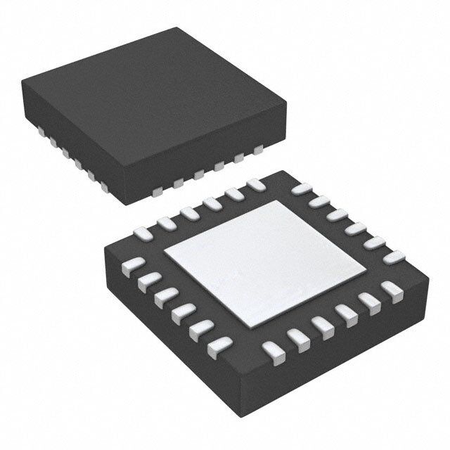
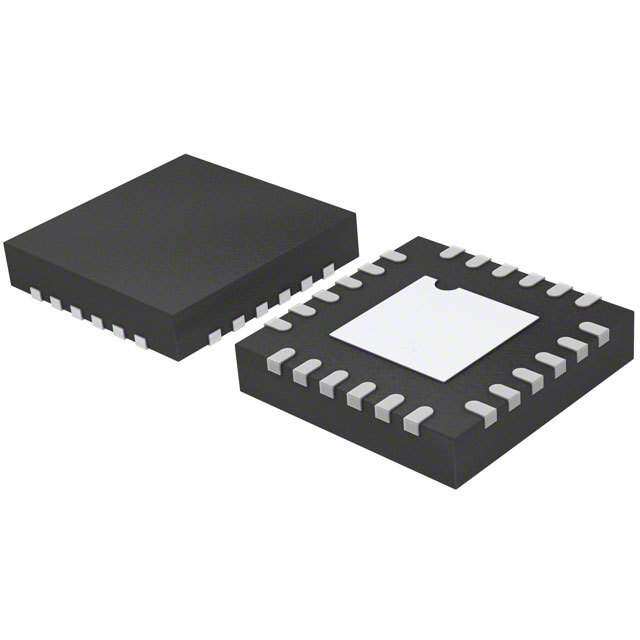
| 封装/外壳 | 24-VFQFN 裸露焊盘 |
| 封装/箱体 | VQFN-24 |
| 工作电源电压 | 4.5 V to 5.5 V |
| 工厂包装数量 | 250 |
| 最大工作温度 | + 85 C |
| 最小工作温度 | - 40 C |
| 本底噪声 | -163dBm/Hz |
| 标准包装 | 1 |
| 测试频率 | 2.14GHz |
| 电压-电源 | 4.5 V ~ 5.5 V |
| 电流-电源 | 235mA |
| 电源电流 | 210 mA |
| 系列 | TRF370315 |
| 调制类型 | Quadrature |
| 输出功率 | -4.5dBm |
| 配用 | /product-detail/zh/TRF3703-15EVM/296-31298-ND/1908653 |
| 频率 | 350 MHz |


- 商务部:美国ITC正式对集成电路等产品启动337调查
- 曝三星4nm工艺存在良率问题 高通将骁龙8 Gen1或转产台积电
- 太阳诱电将投资9.5亿元在常州建新厂生产MLCC 预计2023年完工
- 英特尔发布欧洲新工厂建设计划 深化IDM 2.0 战略
- 台积电先进制程称霸业界 有大客户加持明年业绩稳了
- 达到5530亿美元!SIA预计今年全球半导体销售额将创下新高
- 英特尔拟将自动驾驶子公司Mobileye上市 估值或超500亿美元
- 三星加码芯片和SET,合并消费电子和移动部门,撤换高东真等 CEO
- 三星电子宣布重大人事变动 还合并消费电子和移动部门
- 海关总署:前11个月进口集成电路产品价值2.52万亿元 增长14.8%


PDF Datasheet 数据手册内容提取
TRF370315 TRF370333 www.ti.com SLWS184J–MARCH2006–REVISEDMAY2011 0.35-GHz TO 4-GHz QUADRATURE MODULATORS CheckforSamples:TRF370315,TRF370333 FEATURES APPLICATIONS 1 • 75-dBcSingle-CarrierWCDMAACPR • CellularBaseTransceiverStationTransmit 2 at–11-dBmChannelPower Channel • LowNoiseFloor:–163dBm/Hz • CDMA:IS95,UMTS,CDMA2000,TD-SCDMA • OIP3of23dBm • TDMA:GSM,IS-136,EDGE/UWC-136 • P1dBof9dBm • WirelessLocalLoop • UnadjustedCarrierFeedthroughof–40dBm • WirelessMANWidebandTransceivers • UnadjustedSide-BandSuppressionof–40dBc SPACE THEFINALFRONTIER • SingleSupply:4.5V–5.5VOperation • SiliconGermaniumTechnology RGE PACKAGE (TOPVIEW) • TRF370333With3.3-VCMatI,QBaseband Inputs C D N P D D • TRF370315With1.5-VCMatI,QBaseband C N BI BI N N V G B B G G Inputs 4 3 2 1 0 9 2 2 2 2 2 1 NC 1 18 VCC GND 2 17 GND LOP 3 16 RF_OUT LON 4 15 NC GND 5 14 GND NC 6 13 NC 7 8 9 10 11 12 C D N P D D N N Q Q N N G B B G G B B P0024-04 DESCRIPTION The TRF370315 and TRF370333 are low-noise direct quadrature modulators, capable of converting complex modulated signals from baseband or IF directly up to RF. The TRF370315 and TRF370333 are ideal for high-performance direct RF modulation from 350 MHz up to 4 GHz. These modulators are implemented as a double-balanced mixer. The RF output block consists of a differential to single-ended converter and an RF amplifier capable of driving a single-ended 50-Ω load without any need of external components. The TRF370333 and TRF370315 devices have different common-mode voltage ratings at the I/Q baseband inputs. The TRF370315 requires a 1.5-V common-mode voltage, and the TRF370333 requires a 3.3-V common-mode voltage. 1 Pleasebeawarethatanimportantnoticeconcerningavailability,standardwarranty,anduseincriticalapplicationsofTexas Instrumentssemiconductorproductsanddisclaimerstheretoappearsattheendofthisdatasheet. Alltrademarksarethepropertyoftheirrespectiveowners. 2 PRODUCTIONDATAinformationiscurrentasofpublicationdate. Copyright©2006–2011,TexasInstrumentsIncorporated Products conform to specifications per the terms of the Texas Instruments standard warranty. Production processing does not necessarilyincludetestingofallparameters.
TRF370315 TRF370333 SLWS184J–MARCH2006–REVISEDMAY2011 www.ti.com This integrated circuit can be damaged by ESD. Texas Instruments recommends that all integrated circuits be handled with appropriateprecautions.Failuretoobserveproperhandlingandinstallationprocedurescancausedamage. ESDdamagecanrangefromsubtleperformancedegradationtocompletedevicefailure.Precisionintegratedcircuitsmaybemore susceptibletodamagebecauseverysmallparametricchangescouldcausethedevicenottomeetitspublishedspecifications. FUNCTIONAL BLOCK DIAGRAM C D N P DD D C N BI BI NN N V G B B GG G 4 3 2 1 00 9 2 2 2 2 22 1 NC 1 18 VCC GND 2 17 GND S LOP 3 16 RF_OUT 0/90 LON 4 15 NC GND 5 14 GND NC 6 13 NC 7 8 9 10 11 12 C D N P D D N N Q Q N N G B B G G B B B0175-01 NOTE: NC=Noconnection 2 Copyright©2006–2011,TexasInstrumentsIncorporated
TRF370315 TRF370333 www.ti.com SLWS184J–MARCH2006–REVISEDMAY2011 DEVICE INFORMATION TERMINALFUNCTIONS TERMINAL I/O DESCRIPTION NAME NO. BBIN 22 I In-phaseinput BBIP 21 I In-phaseinput BBQN 9 I In-quadratureinput BBQP 10 I In-quadratureinput 2,5,8,11, GND 12,14,17, – Ground 19,20,23 LON 4 I Localoscillatorinput LOP 3 I Localoscillatorinput 1,6,7,13, NC – Noconnect 15 RF_OUT 16 O RFoutput VCC 18,24 – Powersupply ABSOLUTE MAXIMUM RATINGS(1) Overoperatingfree-airtemperaturerange(unlessotherwisenoted). VALUE(2) UNIT Supplyvoltagerange –0.3Vto6 V DigitalI/Ovoltagerange –0.3VtoV +0.3 V I T Operatingvirtualjunctiontemperaturerange –40to150 °C J T Operatingambienttemperaturerange –40to85 °C A T Storagetemperaturerange –65to150 °C stg Humanbodymodel(HBM) 75 V ESD Electrostaticdischargeratings Chargeddevicemodel(CDM) 75 V (1) StressesbeyondthoselistedunderAbsoluteMaximumRatingsmaycausepermanentdamagetothedevice.Thesearestressratings only,andfunctionaloperationofthedeviceattheseoranyotherconditionsbeyondthoseindicatedunderRecommendedOperating Conditionsisnotimplied.Exposuretoabsolute-maximum-ratedconditionsforextendedperiodsmayaffectdevicereliability. (2) Allvoltagevaluesarewithrespecttonetworkgroundterminal. RECOMMENDED OPERATING CONDITIONS Overoperatingfree-airtemperaturerange(unlessotherwisenoted). MIN NOM MAX UNIT V Power-supplyvoltage 4.5 5 5.5 V CC THERMAL CHARACTERISTICS PARAMETER TESTCONDITIONS VALUE UNIT R Thermalresistance,junction-to-ambient High-Kboard,stillair 29.4 °C/W θJA R Thermalresistance,junction-to-case 18.6 °C/W θJC Copyright©2006–2011,TexasInstrumentsIncorporated 3
TRF370315 TRF370333 SLWS184J–MARCH2006–REVISEDMAY2011 www.ti.com ELECTRICAL CHARACTERISTICS Overoperatingfree-airtemperaturerange(unlessotherwisenoted). PARAMETER TESTCONDITIONS MIN TYP MAX UNIT DCParameters Totalsupplycurrent(1.5VCM) TA=25°C 195 205 ICC mA Totalsupplycurrent(3.3VCM) TA=25°C 210 235 LOInput(50-Ω,Single-Ended) LOfrequencyrange 0.35 4 GHz fLO LOinputpower –5 0 12 dBm LOportreturnloss 15 dB BasebandInputs TRF370333 3.3 VCM IandQinputdccommonvoltage V TRF370315 1.5 BW 1-dBinputfrequencybandwidth 350 MHz Inputimpedance,resistance 10 kΩ TRF370333 ZI(single Inputimpedance,parallelcapacitance 3 pF ended) Inputimpedance,resistance 5 kΩ TRF370315 Inputimpedance,parallelcapacitance 3 pF ELECTRICAL CHARACTERISTICS Overrecommendedoperatingconditions,powersupply=5V,T =25°C,f =350MHzat0dBm,TRF370333(unless A LO otherwisenoted). RFOutputParameters PARAMETER TESTCONDITIONS MIN TYP MAX UNIT TRF370315:OutputRMSvoltageoverinputI(orQ)RMS –4.18 dB voltage G Voltagegain(1) TRF370333:OutputRMSvoltageoverinputI(orQ)RMS –4.0 dB voltage P1dB Outputcompressionpoint 9.4 dBm IP3 OutputIP3 24.5 dBm IP2 OutputIP2 MeasuredatfLO+2×fBB 73.8 dBm Carrierfeedthrough Unadjusted 35.6 dBm Sidebandsuppression Unadjusted 33.8 dBc DConlytoBBinputs,13MHzoffsetfromfLO –158.0 Outputnoisefloor 1.8-MHzoffsetfromfLO;1CWtone;Pout=0dBm –152.6 dBm/Hz 6-MHzoffsetfromfLO;1CWtone;Pout=0dBm –157.4 (1) Single4-MHzCWbasebandinputtone,differential-ended196V . RMS ELECTRICAL CHARACTERISTICS Overrecommendedoperatingconditions,powersupply=5V,T =25°C,f =400MHzat0dBm,TRF370315(unless A LO otherwisenoted). RFOutputParameters PARAMETER TESTCONDITIONS MIN TYP MAX UNIT TRF370315:OutputRMSvoltageoverinputI(orQ)RMS –2.409 dB voltage G Voltagegain(1) TRF370333:OutputRMSvoltageoverinputI(orQ)RMS –1.905 dB voltage P1dB Outputcompressionpoint 9.4 dBm IP3 OutputIP3 20 23 dBm IP2 OutputIP2 MeasuredatfLO+2×fBB 62 dBm Carrierfeedthrough Unadjusted –37 dBm Sidebandsuppression Unadjusted –39 dBc (1) Single4-MHzCWbasebandinputtone,differential-ended196V . RMS 4 Copyright©2006–2011,TexasInstrumentsIncorporated
TRF370315 TRF370333 www.ti.com SLWS184J–MARCH2006–REVISEDMAY2011 ELECTRICAL CHARACTERISTICS Overrecommendedoperatingconditions,powersupply=5V,T =25°C,f =900MHzat0dBm,TRF370315(unless A LO otherwisenoted). RFOutputParameters PARAMETER TESTCONDITIONS MIN TYP MAX UNIT TRF370315:OutputRMSvoltageoverinputI(or –3.552 dB Q)RMSvoltage G Voltagegain(1) TRF370333:OutputRMSvoltageoverinputI(or –2.79 dB Q)RMSvoltage P1dB Outputcompressionpoint 9 dBm IP3 OutputIP3 20 23 dBm IP2 OutputIP2 Measuredatf +2×f 63 dBm LO BB Carrierfeedthrough Unadjusted –37 dBm Sidebandsuppression Unadjusted –42 dBc Outputreturnloss 9 dB DConlytoBBinputs,13MHzoffsetfromf –160.4 LO Outputnoisefloor 1.8-MHzoffsetfromf ;1CWtone;P =0dBm –156.6 dBm/Hz LO out 6-MHzoffsetfromf ;1CWtone;P =0dBm –158.5 LO out 1EDGEsignal,P =–5dBm 0.59% out 1EDGEsignal,P =0dBm 0.63% EVM Errorvectormagnitude(rms) out 1EDGEsignal,P =0dBm,2ndharmonicofLO =–15dBm,3rdhaourtmonicofLO=–33dBm(2) 1% (1) Single4-MHzCWbasebandinputtone,differential-ended196V . RMS (2) Thesecond-andthird-harmonictestsweremadeindependentlyateachfrequency. ELECTRICAL CHARACTERISTICS Overrecommendedoperatingconditions,powersupply=5V,T =25°C,f =1800MHzat0dBm,TRF370315(unless A LO otherwisenoted). RFOutputParameters PARAMETER TESTCONDITIONS MIN TYP MAX UNIT TRF370315:OutputRMSvoltageoverinputI(or –3.345 dB Q)RMSvoltage G Voltagegain(1) TRF370333:OutputRMSvoltageoverinputI(or –2.367 dB Q)RMSvoltage P1dB Outputcompressionpoint 9.5 dBm IP3 OutputIP3 20 23 dBm IP2 OutputIP2 Measuredatf +2×f 55 dBm LO BB Carrierfeedthrough Unadjusted –40 dBm Sidebandsuppression Unadjusted –47 dBc Outputreturnloss 8 dB DConlytoBBinputs,13MHzoffsetfromf –162.6 LO Outputnoisefloor 1.8-MHzoffsetfromf ;1CWtone;P =0dBm –160 dBm/Hz LO out 6-MHzoffsetfromf ;1CWtone;P =0dBm –159.4 LO out 1EDGEsignal,P =–5dBm 0.66% out 1EDGEsignal,P =0dBm 0.74% EVM Errorvectormagnitude(rms) out 1EDGEsignal,P =0dBm,2ndharmonicofLO =–15.5dBm,3rdohuatrmonicofLO=–30dBm(2) 1% (1) Single4-MHzCWbasebandinputtone,differential-ended196V . RMS (2) Thesecond-andthird-harmonictestsweremadeindependentlyateachfrequency. Copyright©2006–2011,TexasInstrumentsIncorporated 5
TRF370315 TRF370333 SLWS184J–MARCH2006–REVISEDMAY2011 www.ti.com ELECTRICAL CHARACTERISTICS Overrecommendedoperatingconditions,powersupply=5V,T =25°C,f =1960MHzat0dBm,TRF370315(unless A LO otherwisenoted). RFOutputParameters PARAMETER TESTCONDITIONS MIN TYP MAX UNIT TRF370315:OutputRMSvoltageoverinputI(or –3.449 dB Q)RMSvoltage G Voltagegain(1) TRF370333:OutputRMSvoltageoverinputI(or –2.479 dB Q)RMSvoltage P1dB Outputcompressionpoint 9.5 dBm OutputIP3,TRF370315 20 23 IP3 dBm OutputIP3,TRF370333 18 20 IP2 OutputIP2 Measuredatf +2×f 55 dBm LO BB Carrierfeedthrough Unadjusted –40 dBm Sidebandsuppression Unadjusted –47 dBc Outputreturnloss 8 dB DConlytoBBinputs,13MHzoffsetfromf –162.6 LO Outputnoisefloor 1.8-MHzoffsetfromf ;1CWtone;P =0dBm –160 dBm/Hz LO out 6-MHzoffsetfromf ;1CWtone;P =0dBm –159.4 LO out 1EDGEsignal,P =–5dBm 0.66% out 1EDGEsignal,P =0dBm 0.74% EVM Errorvectormagnitude(rms) out 1EDGEsignal,P =0dBm,2ndharmonicofLO =–15.5dBm,3rdohuatrmonicofLO=–30dBm(2) 1% (1) Single4-MHzCWbasebandinputtone,differential-ended196V . RMS (2) Thesecond-andthird-harmonictestsweremadeindependentlyateachfrequency. ELECTRICAL CHARACTERISTICS Overrecommendedoperatingconditions,powersupply=5V,T =25°C,f =2140MHzat0dBm,TRF370315(unless A LO otherwisenoted). RFOutputParameters PARAMETER TESTCONDITIONS MIN TYP MAX UNIT TRF370315:OutputRMSvoltageoverinputI(or –3.432 dB Q)RMSvoltage G Voltagegain(1) TRF370333:OutputRMSvoltageoverinputI(or –2.791 dB Q)RMSvoltage P1dB Outputcompressionpoint 9.5 dBm OutputIP3,TRF370315 20 23 IP3 dBm OutputIP3,TRF370333 18 21 IP2 OutputIP2 Measuredatf +2×f 58 dBm LO BB Carrierfeedthrough Unadjusted –40 dBm Sidebandsuppression Unadjusted –47 dBc Outputreturnloss 8.5 dB 20-MHzoffsetfromf ;dconlytoBBinputs –163 LO Outputnoisefloor 20-MHzoffsetfromf ;1WCDMAsignal; dBm/Hz LO –162 P =–20.5dBVrms(IandQinput) in 1WCDMAsignal;P =–13dBm –75.8 out Adjacent-channelpower ACPR 1WCDMAsignal;P =–9dBm –72 dBc ratio out 4WCDMAsignals;P =–23dBmpercarrier –68 out 1WCDMAsignal;P =–13dBm –79 out Alternate-channelpower 1WCDMAsignal;P =–9dBm –80.5 dBc ratio out 4WCDMAsignals;P =–23dBmpercarrier –69 out (1) Single4-MHzCWbasebandinputtone,differential-ended196V . RMS 6 Copyright©2006–2011,TexasInstrumentsIncorporated
TRF370315 TRF370333 www.ti.com SLWS184J–MARCH2006–REVISEDMAY2011 ELECTRICAL CHARACTERISTICS Overrecommendedoperatingconditions,powersupply=5V,T =25°C,f =2500MHzat0dBm,TRF370315(unless A LO otherwisenoted). RFOutputParameters PARAMETER TESTCONDITIONS MIN TYP MAX UNIT TRF370315:OutputRMSvoltageoverinputI(or –2.892 dB Q)RMSvoltage G Voltagegain(1) TRF370333:OutputRMSvoltageoverinputI(or –1.379 dB Q)RMSvoltage P1dB Outputcompressionpoint 9.5 dBm IP3 OutputIP3 18 21 dBm IP2 OutputIP2 Measuredatf +2×f 63 dBm LO BB Carrierfeedthrough Unadjusted –38 dBm Sidebandsuppression Unadjusted –47 dBc (1) Single4-MHzCWbasebandinputtone,differential-ended196V . RMS ELECTRICAL CHARACTERISTICS Overrecommendedoperatingconditions,powersupply=5V,T =25°C,f =3600MHzat0dBm,TRF370315(unless A LO otherwisenoted). RFOutputParameters PARAMETER TESTCONDITIONS MIN TYP MAX UNIT TRF370315:OutputRMSvoltageoverinputI(or –1.265 dB Q)RMSvoltage G Voltagegain(1) TRF370333:OutputRMSvoltageoverinputI(or 1.529 dB Q)RMSvoltage P1dB Outputcompressionpoint 9.5 dBm IP3 OutputIP3 20 23 dBm IP2 OutputIP2 Measuredatf +2×f 63 dBm LO BB Carrierfeedthrough Unadjusted –41 dBm Sidebandsuppression Unadjusted –45 dBc (1) Single4-MHzCWbasebandinputtone,differential-ended196V . RMS ELECTRICAL CHARACTERISTICS Overrecommendedoperatingconditions,powersupply=5V,T =25°C,f =4000MHzat0dBm,TRF370315(unless A LO otherwisenoted). RFOutputParameters PARAMETER TESTCONDITIONS MIN TYP MAX UNIT TRF370315:OutputRMSvoltageoverinputI(or –2.242 dB Q)RMSvoltage G Voltagegain(1) TRF370333:OutputRMSvoltageoverinputI(or 0.543 dB Q)RMSvoltage P1dB Outputcompressionpoint 9 dBm IP3 OutputIP3 19 22 dBm IP2 OutputIP2 Measuredatf +2×f 50 dBm LO BB Carrierfeedthrough Unadjusted –37 dBm Sidebandsuppression Unadjusted –40 dBc (1) Single4-MHzCWbasebandinputtone,differential-ended196V . RMS Copyright©2006–2011,TexasInstrumentsIncorporated 7
TRF370315 TRF370333 SLWS184J–MARCH2006–REVISEDMAY2011 www.ti.com TYPICAL CHARACTERISTICS OUTPUTPOWER OUTPUTPOWER vs vs BASEBANDVOLTAGE FREQUENCYANDTEMPERATURE 15 0 TTRRFF33770033--1155 TTRRFF33770033--3333 −1 10 –40°C m −2 B d m -z 5 dB −3 wer at 1.8 GH 0 ut Power − −−54 25°C 85°C ut Po -5 Outp −6 Outp -10 − UT −7 - O UT P −8 O P -15 −9 LO = 0 dB VCC = 5 V -20 −10 0.01 0.1 1 0 500 1000 1500 2000 2500 3000 3500 4000 4500 VBB-Baseband Voltage, Single-Ended, RMS-V f − Frequency − MHz G010 Figure1. Figure2. OUTPUTPOWER OUTPUTPOWER vs vs FREQUENCYANDSUPPLYVOLTAGE FREQUENCYANDLOPOWER 0 0 5.5 V −1 −1 −2 0 dBm m m dB −3 dB −2 5 dBm − − er −4 4.5 V 5 V er w w −3 o o P P ut −5 ut utp −6 utp −4 –5 dBm O O − − UT −7 UT −5 O O P P −8 −6 −9 LO = 0 dB VCC = 5 V TA = 25°C TA = 25°C −10 −7 0 500 1000 1500 2000 2500 3000 3500 4000 4500 0 500 1000 1500 2000 2500 3000 3500 4000 4500 f − Frequency − MHz f − Frequency − MHz G011 G012 Figure3. Figure4. 8 Copyright©2006–2011,TexasInstrumentsIncorporated
TRF370315 TRF370333 www.ti.com SLWS184J–MARCH2006–REVISEDMAY2011 TYPICAL CHARACTERISTICS (continued) P1dB P1dB vs vs FREQUENCYANDTEMPERATURE FREQUENCYANDSUPPLYVOLTAGE 14 12 LO = 0 dB VCC = 5 V 5.5 V 12 10 10 5 V 8 m m 4.5 V B 8 B − d 25°C –40°C 85°C − d 6 B B d 6 d 1 1 P P 4 4 2 2 LO = 0 dB TA = 25°C 0 0 0 500 1000 1500 2000 2500 3000 3500 4000 4500 0 500 1000 1500 2000 2500 3000 3500 4000 4500 f − Frequency − MHz f − Frequency − MHz G001 G002 Figure5. Figure6. TRF370315 P1dB OIP3 vs vs FREQUENCYANDLOPOWER FREQUENCYANDTEMPERATURE 12 30 28 –5 dBm 25°C 10 26 85°C 5 dBm 24 8 m 0 dBm m 22 B B d d − 6 − 20 B 3 d P 1 OI 18 P 4 –40°C 16 14 2 VCC = 5 V 12 LO = 0 dBm TA = 25°C VCC = 5 V 0 10 0 500 1000 1500 2000 2500 3000 3500 4000 4500 0 500 1000 1500 2000 2500 3000 3500 4000 4500 f − Frequency − MHz f − Frequency − MHz G003 G014 Figure7. Figure8. Copyright©2006–2011,TexasInstrumentsIncorporated 9
TRF370315 TRF370333 SLWS184J–MARCH2006–REVISEDMAY2011 www.ti.com TYPICAL CHARACTERISTICS (continued) TRF370333 TRF370315 OIP3 OIP3 vs vs FREQUENCYANDTEMPERATURE FREQUENCYANDSUPPLYVOLTAGE 30 30 28 28 5 V 85°C 25°C 4.5 V 26 26 24 24 m 22 m 22 B B d d − 20 − 20 3 3 P P 5.5 V OI 18 OI 18 –40°C 16 16 14 14 12 LO = 0 dB 12 LO = 0 dBm VCC = 5 V TA = 25°C 10 10 0 500 1000 1500 2000 2500 3000 3500 4000 4500 0 500 1000 1500 2000 2500 3000 3500 4000 4500 f − Frequency − MHz f − Frequency − MHz G027 G015 Figure9. Figure10. TRF370333 TRF370315 OIP3 OIP3 vs vs FREQUENCYANDSUPPLYVOLTAGE FREQUENCYANDLOPOWER 40 30 LO = 0 dB 5 V TA = 25°C 28 +5 dBm 36 26 4.5 V 32 24 m m 22 B 28 B –5 dBm d d − − 20 3 3 P 24 P 0 dBm OI OI 18 20 16 14 16 5.5 V 12 VCC = 5 V TA = 25°C 12 10 0 500 1000 1500 2000 2500 3000 3500 4000 4500 0 500 1000 1500 2000 2500 3000 3500 4000 4500 f − Frequency − MHz f − Frequency − MHz G028 G013 Figure11. Figure12. 10 Copyright©2006–2011,TexasInstrumentsIncorporated
TRF370315 TRF370333 www.ti.com SLWS184J–MARCH2006–REVISEDMAY2011 TYPICAL CHARACTERISTICS (continued) TRF370333 OIP3 UNADJUSTEDSIDEBANDSUPPRESSION vs vs FREQUENCYANDLOPOWER FREQUENCYANDTEMPERATURE 40 0 VCC = 5 V c LO = 0 dB 36 TA = 25°C 0 dBm n − dB −10 PVOCCU T= = 5 – V3 dBm o si 32 s e pr −20 p − dBm 28 and Su −30 OIP3 24 +5 dBm ed Sideb −40 85°C 25°C 20 st u dj –5 dBm a 16 Un −50 S − –40°C S 12 −60 0 500 1000 1500 2000 2500 3000 3500 4000 4500 0 500 1000 1500 2000 2500 3000 3500 4000 4500 f − Frequency − MHz f − Frequency − MHz G029 G007 Figure13. Figure14. UNADJUSTEDSIDEBANDSUPPRESSION UNADJUSTEDSIDEBANDSUPPRESSION vs vs FREQUENCYANDSUPPLYVOLTAGE FREQUENCYANDLOPOWER 0 0 c LO = 0 dB c VCC = 5 V B B d POUT = –3 dBm d POUT = –3 dBm n − −10 TA = 25°C n − −10 TA = 25°C o o si si s s e e pr −20 pr −20 p p u u S S d d n n a −30 a −30 b b e e d d –5 dBm Si 5 V Si 0 dBm ed −40 5.5 V ed −40 st st u u dj dj a a Un −50 Un −50 − − S S 5 dBm S 4.5 V S −60 −60 0 500 1000 1500 2000 2500 3000 3500 4000 4500 0 500 1000 1500 2000 2500 3000 3500 4000 4500 f − Frequency − MHz f − Frequency − MHz G008 G009 Figure15. Figure16. Copyright©2006–2011,TexasInstrumentsIncorporated 11
TRF370315 TRF370333 SLWS184J–MARCH2006–REVISEDMAY2011 www.ti.com TYPICAL CHARACTERISTICS (continued) ADJUSTEDSIDEBANDSUPPRESSION ADJUSTEDSIDEBANDSUPPRESSION vs vs FREQUENCYANDTEMPERATURE FREQUENCYANDTEMPERATURE −20 −20 c Adj at 942.6 MHz c Adj at 1900 MHz B B − d −30 VCC = 5 V − d −30 VCC = 5 V n n o o si si s s pre −40 pre −40 p p u u S S d d n −50 n −50 ba –40°C ba e e d Sid −60 25°C d Sid −60 85°C e e –40°C st st u u dj dj 25°C A −70 A −70 − − S S S S 85°C −80 −80 900 920 940 960 980 1000 1850 1870 1890 1910 1930 1950 f − Frequency − MHz f − Frequency − MHz G016 G017 Figure17. Figure18. ADJUSTEDSIDEBANDSUPPRESSION NOISEAT13-MHzOFFSET(dBm/Hz) vs vs FREQUENCYANDTEMPERATURE FREQUENCYANDSUPPLYVOLTAGE −20 −154 POUT = –5 dBm Bc Adj at 2140 MHz LO = 5 dBm n − d −30 VCC = 5 V Hz −156 TA = 25°C ssio Bm/ −158 5.5 V pre −40 − d Sup set −160 and −50 85°C z Off 5 V eb –40°C MH −162 sted Sid −60 e at 13- −164 u s dj oi 4.5 V A −70 N − −166 S S 25°C −80 −168 2100 2120 2140 2160 2180 2200 0.0 0.5 1.0 1.5 2.0 2.5 3.0 3.5 4.0 f − Frequency − MHz f − Frequency − GHz G018 G019 Figure19. Figure20. 12 Copyright©2006–2011,TexasInstrumentsIncorporated
TRF370315 TRF370333 www.ti.com SLWS184J–MARCH2006–REVISEDMAY2011 TYPICAL CHARACTERISTICS (continued) NOISEAT13-MHzOFFSET(dBm/Hz) NOISEAT13-MHzOFFSET(dBm/Hz) vs vs FREQUENCYANDTEMPERATURE FREQUENCYANDTEMPERATURE −154 −154 −156 85°C −156 z z m/H m/H 85°C B −158 B −158 d 25°C d set − −160 set − −160 25°C Off Off z z H H M −162 M −162 3- 3- 1 1 e at −164 e at −164 Nois –40°C Nois –40°C −166 POUT = 0 dBm −166 POUT = –5 dBm LO = 5 dBm LO = 5 dBm VCC = 5 V VCC = 5 V −168 −168 0.0 0.5 1.0 1.5 2.0 2.5 3.0 3.5 4.0 0.0 0.5 1.0 1.5 2.0 2.5 3.0 3.5 4.0 f − Frequency − GHz f − Frequency − GHz G020 G021 Figure21. Figure22. NOISEAT13-MHzOFFSET(dBm/Hz) UNADJUSTEDCARRIERFEEDTHROUGH vs vs FREQUENCYANDTEMPERATURE FREQUENCYANDSUPPLYVOLTAGE −154 0 POUT = –10 dBm m LO = 0 dB LO = 5 dBm B −10 TA = 25°C Hz −156 VCC = 5 V h − d Offset − dBm/ −−116508 25°C 85°C er Feedthroug −−−432000 5.5 V 5 V MHz −162 Carri 3- d −50 1 e 4.5 V se at −164 djust −60 oi na N U −166 − −70 –40°C S C −168 −80 0.0 0.5 1.0 1.5 2.0 2.5 3.0 3.5 4.0 0 500 1000 1500 2000 2500 3000 3500 4000 4500 f − Frequency − GHz f − Frequency − MHz G022 G025 Figure23. Figure24. Copyright©2006–2011,TexasInstrumentsIncorporated 13
TRF370315 TRF370333 SLWS184J–MARCH2006–REVISEDMAY2011 www.ti.com TYPICAL CHARACTERISTICS (continued) UNADJUSTEDCARRIERFEEDTHROUGH vs FREQUENCYANDTEMPERATURE 0 LO = 0 dB m B −10 VCC = 5 V d − h g −20 u o hr dt −30 e 85°C e F er −40 arri C d −50 e ust 25°C dj −60 a n U − −70 –40°C S C −80 0 500 1000 1500 2000 2500 3000 3500 4000 4500 f − Frequency − MHz G026 Figure25. 14 Copyright©2006–2011,TexasInstrumentsIncorporated
TRF370315 TRF370333 www.ti.com SLWS184J–MARCH2006–REVISEDMAY2011 APPLICATION INFORMATION AND EVALUATION BOARD Basic Connections • SeeFigure26forproperconnectionoftheTRF3703315andTRF370333modulator. • Connect a single power supply (4.5 V–5.5 V) to pins 18 and 24. These pins should be decoupled as shown onpins4,5,6,and7. • Connectpins2,5,8,11,12,14,17,19,20,and23toGND. • Connect a single-ended LO source of desired frequency to LOP (amplitude between –5 dBm and 12 dBm). Thisshouldbeac-coupledthrougha100-pFcapacitor. • Terminatetheac-coupledLONwith50Ω toGND. • Connectabasebandsignaltopins21=I,22=I,10=Q,and9=Q. • The differential baseband inputs should be set to the proper level, 3.3 V for the TRF370333 or 1.5 V for the TRF370315. • RF_OUT, pin 16, can be fed to a spectrum analyzer set to the desired frequency, LO ± baseband signal. This pinshouldalsobeac-coupledthrougha100-pFcapacitor. • AllNCpinscanbeleftfloating. ESDSensitivity RF devices may be extremely sensitive to electrostatic discharge (ESD). To prevent damage from ESD, devices should be stored and handled in a way that prevents the build-up of electrostatic voltages that exceed the rated level. Rated ESD levels should also not be exceeded while the device is installed on a printed circuit board (PCB).FollowtheseguidelinesforoptimalESDprotection: • Low ESD performance is not uncommon in RF ICs; see the Absolute Maximum Ratings table. Therefore, customers’ESDprecautionsshouldbeconsistentwiththeseratings. • The device should be robust once assembled onto the PCB unless external inputs (connectors, etc.) directly connectthedevicepinstooff-boardcircuits. Copyright©2006–2011,TexasInstrumentsIncorporated 15
TRF370315 TRF370333 SLWS184J–MARCH2006–REVISEDMAY2011 www.ti.com J3 J4 IN IP 1 1 SMA_END SMA_END 5432 2345 W1 W2 2POS_JUMPER 2POS_JUMPER R2 R3 C6 C5 C7 C4 + + 1000 pF 0 0 1000 pF 4.7mF 4.7uF J1 4 3 2 1 0 9 LOP 2 2 2 2 2 1 C1 O D N P D D 1 L N I I N N SMA_END 1 cc G G G 18 100 pF NC V VccMOD J7 2 17 RF_OUT 5432 GND GND C3 3 16 R1 1 LOP RF_OUT SMA_END U1 4 TRF3703 15 0 100 pF LON NC C8 C9 J2 5 14 2345 GND GND LON 0.1mF 0.1mF C2 6 NC NC 13 (Note 1) (Note 1) 1 SMA_END D D D C N N P N N 100 pF N G Q Q G G 5432 7 8 9 10 11 12 R4 R5 0 0 J5 J6 QN QP 1 1 SMA_END SMA_END 5432 2345 S0214-01 (1) Donotinstall. Figure26. TRF3703EVMSchematic 16 Copyright©2006–2011,TexasInstrumentsIncorporated
TRF370315 TRF370333 www.ti.com SLWS184J–MARCH2006–REVISEDMAY2011 Figure27showsthetopviewoftheTRF3703EVMboard. GND +5 V +5 V GND BBIN BBIP LOP RF_OUT LON 50W BBQP BBQN K001 Figure27. TRF3703EVMBoardLayout Table1.BillofMaterialsforTRF3703EVM Value Footprint QTY PartNumber Vendor Digi-KeyNumber REFDES Not Installed Tantalum 3216 2 T491A475K010AS KEMET 399-1561-1-ND C6,C7 4.7-μF,10-V, 10%capacitor 1000-pF,50-V, 603 2 ECJ-1VC1H102J Panasonic PCC2151CT-ND C4,C5 5%capacitor 100-pF,50-V, 603 3 ECJ-1VC1H101J Panasonic PCC101ACVCT-ND C1,C2,C3 5%capacitor Capacitor 603 0 C8,C9 0-Ωresistor, 603 5 ERJ-3GEY0R00V Panasonic P0.0GCT-ND R1,R2,R3, 1/10-W,5% R4,R5 Copyright©2006–2011,TexasInstrumentsIncorporated 17
TRF370315 TRF370333 SLWS184J–MARCH2006–REVISEDMAY2011 www.ti.com Table1.BillofMaterialsforTRF3703EVM(continued) Value Footprint QTY PartNumber Vendor Digi-KeyNumber REFDES Not Installed TRF3703 24-QFN-PP- 1 TI U1 4X4MM SMAconnectors SMA_END_ 6 16F3627 Newark 142-0711-821 J1,J2,J3, SMALL J4,J5,J6, J7 2POS_HEADER 2POS_JUMP 2 HTSW-150-07-L-S SAMTEC N/A W1,W2 GSM Applications The TRF370315 and TRF370333 are suited for GSM applications because of the high linearity and low noise level over the entire recommended operating range. These devices also have excellent EVM performance, which makesthemidealforthestringentGSM/EDGEapplications. WCDMA Applications The TRF370315 and TRF370333 are also optimized for WCDMA applications where both adjacent-channel power ratio (ACPR) and noise density are critically important. Using Texas instruments’ DAC568X series of high-performance digital-to-analog converters as depicted in Figure 28, excellent ACPR levels were measured with one-, two-, and four-WCDMA carriers. See Electrical Characteristics, f = 2140 MHz for exact ACPR LO values. 16 TRF3703 RF_OUT DAC5687 I/Q Modulator 16 CLK1 CLK2 VCXO TRF3761 CDCM7005 PLL Clock Gen LO Generator Ref Osc B0176-01 Figure28. TypicalTransmitSetupBlockDiagram 18 Copyright©2006–2011,TexasInstrumentsIncorporated
TRF370315 TRF370333 www.ti.com SLWS184J–MARCH2006–REVISEDMAY2011 DEFINITION OF SPECIFICATIONS Unadjusted Carrier Feedthrough This specification measures the amount by which the local oscillator component is attenuated in the output spectrum of the modulator relative to the carrier. This further assumes that the baseband inputs delivered to the pins of the TRF370315 and TRF370333 are perfectly matched to have the same dc offset (VCM). This includes allfourbasebandinputs:I,I,Q,andQ.ThisismeasuredindBm. Adjusted (Optimized) Carrier Feedthrough Thisdiffersfromtheunadjustedsuppressionnumberinthatthebasebandinputdcoffsetsareiterativelyadjusted around their theoretical value of VCM to yield the maximum suppression of the LO component in the output spectrum.ThisismeasuredindBm. Unadjusted Sideband Suppression This specification measures the amount by which the unwanted sideband of the input signal is attenuated in the output of the modulator, relative to the wanted sideband. This further assumes that the baseband inputs delivered to the modulator input pins are perfectly matched in amplitude and are exactly 90° out of phase. This is measuredindBc. Adjusted (Optimized) Sideband Suppression Thisdiffersfromtheunadjustedsidebandsuppressioninthatthebasebandinputsareiterativelyadjustedaround theirtheoreticalvaluestomaximizetheamountofsidebandsuppression.ThisismeasuredindBc. Suppressions Overtemperature This specification assumes that the user has gone though the optimization process for the suppression in question, and set the optimal settings for the I, Q inputs. This specification then measures the suppression when temperatureconditionschangeaftertheinitialcalibrationisdone. Figure 29 shows a simulated output and illustrates the respective definitions of various terms used in this data sheet.Thegraphassumesabasebandinputof50kHz. 10 POUT 0 −10 −20 3RD LSB SBS C 2ND USB m (dBc) (dBc) (dBm) (dBc) B d − −30 r e w o −40 P − P −50 −60 LSB USB −70 3RD LSB (Undesired) (Desired) 3RD USB 2ND LSB Carrier 2ND USB −80 −200 −150 −100 −50 0 50 100 150 200 f − Frequency Offset − kHz (Relative to Carrier) G024 Figure29. GraphicalIllustrationofCommonTerms Copyright©2006–2011,TexasInstrumentsIncorporated 19
TRF370315 TRF370333 SLWS184J–MARCH2006–REVISEDMAY2011 www.ti.com REVISION HISTORY NOTE:Pagenumbersforpreviousrevisionsmaydifferfrompagenumbersinthecurrentversion. ChangesfromRevisionI(July,2010)toRevisionJ Page • Changedvoltagegainspecificationsforf =350-MHzperformancedata ......................................................................... 4 LO • Updatedvoltagegainspecificationsforf =400-MHzperformancedata .......................................................................... 4 LO • Revisedvoltagegainspecificationsforf =900-MHzperformancedata ........................................................................... 5 LO • Changedvoltagegainspecificationsforf =1800-MHzperformancedata ....................................................................... 5 LO • Revisedvoltagegainspecificationsforf =1960-MHzperformancedata ......................................................................... 6 LO • Updatedvoltagegainspecificationsforf =2140-MHzperformancedata ........................................................................ 6 LO • Revisedvoltagegainspecificationsforf =2500-MHzperformancedata ......................................................................... 7 LO • Changedvoltagegainspecificationsforf =3600-MHzperformancedata ....................................................................... 7 LO • Updatedvoltagegainspecificationsforf =4000-MHzperformancedata ........................................................................ 7 LO • ReplacedFigure1 ................................................................................................................................................................ 8 ChangesfromRevisionH(January,2010)toRevisionI Page • Changeddocumenttitletoreflect0.35-GHzminimumoperatinglevel ................................................................................ 1 • UpdatedDescriptionsectiontoreflect350-MHzminimumoperation................................................................................... 1 • ChangedLOfrequencyrangeminimumspecificationfrom0.4GHzto0.35GHz ............................................................... 4 • AddedElectricalCharacteristicstableforf =350-MHzperformancedata ....................................................................... 4 LO 20 Copyright©2006–2011,TexasInstrumentsIncorporated
PACKAGE OPTION ADDENDUM www.ti.com 6-Feb-2020 PACKAGING INFORMATION Orderable Device Status Package Type Package Pins Package Eco Plan Lead/Ball Finish MSL Peak Temp Op Temp (°C) Device Marking Samples (1) Drawing Qty (2) (6) (3) (4/5) TRF370315IRGER ACTIVE VQFN RGE 24 3000 Green (RoHS NIPDAU Level-2-260C-1 YEAR -40 to 85 TRF37 & no Sb/Br) 0315 TRF370315IRGET ACTIVE VQFN RGE 24 250 Green (RoHS NIPDAU Level-2-260C-1 YEAR -40 to 85 TRF37 & no Sb/Br) 0315 TRF370333IRGER ACTIVE VQFN RGE 24 3000 Green (RoHS NIPDAU Level-2-260C-1 YEAR -40 to 85 TRF37 & no Sb/Br) 0333 TRF370333IRGET ACTIVE VQFN RGE 24 250 Green (RoHS NIPDAU Level-2-260C-1 YEAR -40 to 85 TRF37 & no Sb/Br) 0333 TRF370333IRGETG4 ACTIVE VQFN RGE 24 250 Green (RoHS NIPDAU Level-2-260C-1 YEAR -40 to 85 TRF37 & no Sb/Br) 0333 (1) The marketing status values are defined as follows: ACTIVE: Product device recommended for new designs. LIFEBUY: TI has announced that the device will be discontinued, and a lifetime-buy period is in effect. NRND: Not recommended for new designs. Device is in production to support existing customers, but TI does not recommend using this part in a new design. PREVIEW: Device has been announced but is not in production. Samples may or may not be available. OBSOLETE: TI has discontinued the production of the device. (2) RoHS: TI defines "RoHS" to mean semiconductor products that are compliant with the current EU RoHS requirements for all 10 RoHS substances, including the requirement that RoHS substance do not exceed 0.1% by weight in homogeneous materials. Where designed to be soldered at high temperatures, "RoHS" products are suitable for use in specified lead-free processes. TI may reference these types of products as "Pb-Free". RoHS Exempt: TI defines "RoHS Exempt" to mean products that contain lead but are compliant with EU RoHS pursuant to a specific EU RoHS exemption. Green: TI defines "Green" to mean the content of Chlorine (Cl) and Bromine (Br) based flame retardants meet JS709B low halogen requirements of <=1000ppm threshold. Antimony trioxide based flame retardants must also meet the <=1000ppm threshold requirement. (3) MSL, Peak Temp. - The Moisture Sensitivity Level rating according to the JEDEC industry standard classifications, and peak solder temperature. (4) There may be additional marking, which relates to the logo, the lot trace code information, or the environmental category on the device. (5) Multiple Device Markings will be inside parentheses. Only one Device Marking contained in parentheses and separated by a "~" will appear on a device. If a line is indented then it is a continuation of the previous line and the two combined represent the entire Device Marking for that device. (6) Lead/Ball Finish - Orderable Devices may have multiple material finish options. Finish options are separated by a vertical ruled line. Lead/Ball Finish values may wrap to two lines if the finish value exceeds the maximum column width. Addendum-Page 1
PACKAGE OPTION ADDENDUM www.ti.com 6-Feb-2020 Important Information and Disclaimer:The information provided on this page represents TI's knowledge and belief as of the date that it is provided. TI bases its knowledge and belief on information provided by third parties, and makes no representation or warranty as to the accuracy of such information. Efforts are underway to better integrate information from third parties. TI has taken and continues to take reasonable steps to provide representative and accurate information but may not have conducted destructive testing or chemical analysis on incoming materials and chemicals. TI and TI suppliers consider certain information to be proprietary, and thus CAS numbers and other limited information may not be available for release. In no event shall TI's liability arising out of such information exceed the total purchase price of the TI part(s) at issue in this document sold by TI to Customer on an annual basis. Addendum-Page 2
PACKAGE MATERIALS INFORMATION www.ti.com 22-Nov-2018 TAPE AND REEL INFORMATION *Alldimensionsarenominal Device Package Package Pins SPQ Reel Reel A0 B0 K0 P1 W Pin1 Type Drawing Diameter Width (mm) (mm) (mm) (mm) (mm) Quadrant (mm) W1(mm) TRF370315IRGER VQFN RGE 24 3000 330.0 12.4 4.3 4.3 1.5 8.0 12.0 Q1 TRF370315IRGET VQFN RGE 24 250 330.0 12.4 4.3 4.3 1.5 8.0 12.0 Q1 TRF370333IRGER VQFN RGE 24 3000 330.0 12.4 4.3 4.3 1.5 8.0 12.0 Q1 TRF370333IRGET VQFN RGE 24 250 330.0 12.4 4.3 4.3 1.5 8.0 12.0 Q1 PackMaterials-Page1
PACKAGE MATERIALS INFORMATION www.ti.com 22-Nov-2018 *Alldimensionsarenominal Device PackageType PackageDrawing Pins SPQ Length(mm) Width(mm) Height(mm) TRF370315IRGER VQFN RGE 24 3000 367.0 367.0 38.0 TRF370315IRGET VQFN RGE 24 250 367.0 367.0 38.0 TRF370333IRGER VQFN RGE 24 3000 367.0 367.0 38.0 TRF370333IRGET VQFN RGE 24 250 367.0 367.0 38.0 PackMaterials-Page2
GENERIC PACKAGE VIEW RGE 24 VQFN - 1 mm max height PLASTIC QUAD FLATPACK - NO LEAD Images above are just a representation of the package family, actual package may vary. Refer to the product data sheet for package details. 4204104/H
PACKAGE OUTLINE RGE0024B VQFN - 1 mm max height SCALE 3.000 PLASTIC QUAD FLATPACK - NO LEAD A 4.1 B 3.9 0.5 0.3 PIN 1 INDEX AREA 4.1 3.9 0.3 0.2 DETAIL OPTIONAL TERMINAL TYPICAL C 1 MAX SEATING PLANE 0.05 0.00 0.08 C 2X 2.5 2.45 0.1 (0.2) TYP 7 12 EXPOSED SEE TERMINAL THERMAL PAD DETAIL 6 13 2X 25 SYMM 2.5 1 18 0.3 20X 0.5 24X 0.2 24 SYMM 19 0.1 C A B PIN 1 ID 0.05 (OPTIONAL) 0.5 24X 0.3 4219013/A 05/2017 NOTES: 1. All linear dimensions are in millimeters. Any dimensions in parenthesis are for reference only. Dimensioning and tolerancing per ASME Y14.5M. 2. This drawing is subject to change without notice. 3. The package thermal pad must be soldered to the printed circuit board for thermal and mechanical performance. www.ti.com
EXAMPLE BOARD LAYOUT RGE0024B VQFN - 1 mm max height PLASTIC QUAD FLATPACK - NO LEAD ( 2.45) SYMM 24 19 24X (0.6) 1 18 24X (0.25) (R0.05) TYP 25 SYMM (3.8) 20X (0.5) 13 6 ( 0.2) TYP VIA 7 12 (0.975) TYP (3.8) LAND PATTERN EXAMPLE EXPOSED METAL SHOWN SCALE:15X 0.07 MAX 0.07 MIN ALL AROUND ALL AROUND SOLDER MASK METAL OPENING EXPMOESTEADL SOOPLEDNEINRG MASK EXPMOESTEADL MSOELTDAEL RU NMDAESRK NON SOLDER MASK SOLDER MASK DEFINED DEFINED (PREFERRED) SOLDER MASK DETAILS 4219013/A 05/2017 NOTES: (continued) 4. This package is designed to be soldered to a thermal pad on the board. For more information, see Texas Instruments literature number SLUA271 (www.ti.com/lit/slua271). 5. Vias are optional depending on application, refer to device data sheet. If any vias are implemented, refer to their locations shown on this view. It is recommended that vias under paste be filled, plugged or tented. www.ti.com
EXAMPLE STENCIL DESIGN RGE0024B VQFN - 1 mm max height PLASTIC QUAD FLATPACK - NO LEAD 4X ( 1.08) (0.64) TYP 24 19 24X (0.6) 1 25 18 24X (0.25) (R0.05) TYP (0.64) TYP SYMM (3.8) 20X (0.5) 13 6 METAL TYP 7 12 SYMM (3.8) SOLDER PASTE EXAMPLE BASED ON 0.125 mm THICK STENCIL EXPOSED PAD 25 78% PRINTED SOLDER COVERAGE BY AREA UNDER PACKAGE SCALE:20X 4219013/A 05/2017 NOTES: (continued) 6. Laser cutting apertures with trapezoidal walls and rounded corners may offer better paste release. IPC-7525 may have alternate design recommendations. www.ti.com
IMPORTANTNOTICEANDDISCLAIMER TI PROVIDES TECHNICAL AND RELIABILITY DATA (INCLUDING DATASHEETS), DESIGN RESOURCES (INCLUDING REFERENCE DESIGNS), APPLICATION OR OTHER DESIGN ADVICE, WEB TOOLS, SAFETY INFORMATION, AND OTHER RESOURCES “AS IS” AND WITH ALL FAULTS, AND DISCLAIMS ALL WARRANTIES, EXPRESS AND IMPLIED, INCLUDING WITHOUT LIMITATION ANY IMPLIED WARRANTIES OF MERCHANTABILITY, FITNESS FOR A PARTICULAR PURPOSE OR NON-INFRINGEMENT OF THIRD PARTY INTELLECTUAL PROPERTY RIGHTS. These resources are intended for skilled developers designing with TI products. You are solely responsible for (1) selecting the appropriate TI products for your application, (2) designing, validating and testing your application, and (3) ensuring your application meets applicable standards, and any other safety, security, or other requirements. These resources are subject to change without notice. TI grants you permission to use these resources only for development of an application that uses the TI products described in the resource. Other reproduction and display of these resources is prohibited. No license is granted to any other TI intellectual property right or to any third party intellectual property right. TI disclaims responsibility for, and you will fully indemnify TI and its representatives against, any claims, damages, costs, losses, and liabilities arising out of your use of these resources. TI’s products are provided subject to TI’s Terms of Sale (www.ti.com/legal/termsofsale.html) or other applicable terms available either on ti.com or provided in conjunction with such TI products. TI’s provision of these resources does not expand or otherwise alter TI’s applicable warranties or warranty disclaimers for TI products. Mailing Address: Texas Instruments, Post Office Box 655303, Dallas, Texas 75265 Copyright © 2020, Texas Instruments Incorporated