ICGOO在线商城 > 集成电路(IC) > PMIC - 稳压器 - 线性 > TPS7A3501DRVT
 Datasheet下载
- 型号: TPS7A3501DRVT
- 制造商: Texas Instruments
- 库位|库存: xxxx|xxxx
- 要求:
| 数量阶梯 | 香港交货 | 国内含税 |
| +xxxx | $xxxx | ¥xxxx |
查看当月历史价格
查看今年历史价格
TPS7A3501DRVT产品简介:
ICGOO电子元器件商城为您提供TPS7A3501DRVT由Texas Instruments设计生产,在icgoo商城现货销售,并且可以通过原厂、代理商等渠道进行代购。 TPS7A3501DRVT价格参考¥14.49-¥20.04。Texas InstrumentsTPS7A3501DRVT封装/规格:PMIC - 稳压器 - 线性, Linear Voltage Regulator IC Positive Adjustable 1 Output 1.21 V ~ 4.5 V 1A 6-SON (2x2)。您可以下载TPS7A3501DRVT参考资料、Datasheet数据手册功能说明书,资料中有TPS7A3501DRVT 详细功能的应用电路图电压和使用方法及教程。
| 参数 | 数值 |
| 产品目录 | 集成电路 (IC)半导体 |
| 描述 | IC REG LDO ADJ 1A 6SONActive Filter Low Noise High PSRR 1A Active Filter |
| DevelopmentKit | TPS7A3501EVM-547 |
| 产品分类 | |
| 品牌 | Texas Instruments |
| 产品手册 | |
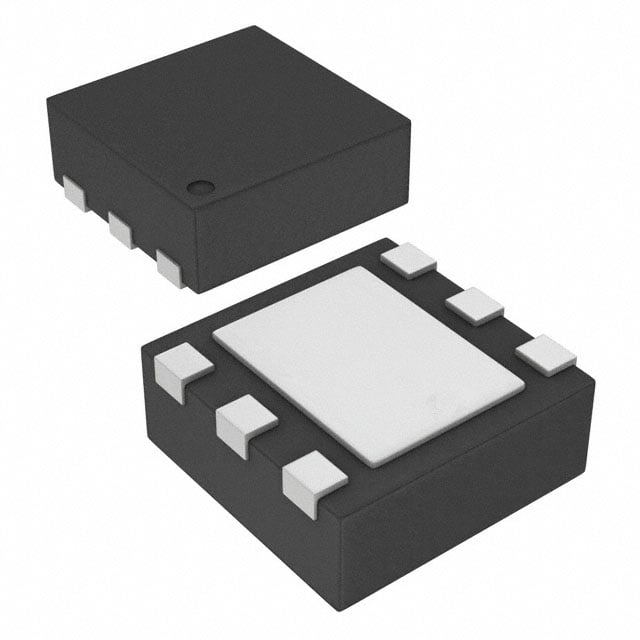
| 产品图片 |
|
| rohs | 符合RoHS无铅 / 符合限制有害物质指令(RoHS)规范要求 |
| 产品系列 | 有源滤波器,Texas Instruments TPS7A3501DRVT- |
| 数据手册 | |
| 产品型号 | TPS7A3501DRVT |
| 产品种类 | 有源滤波器 |
| 供应商器件封装 | 6-SON(2x2) |
| 其它名称 | 296-37133-2 |
| 制造商产品页 | http://www.ti.com/general/docs/suppproductinfo.tsp?distId=10&orderablePartNumber=TPS7A3501DRVT |
| 包装 | 带卷 (TR) |
| 商标 | Texas Instruments |
| 安装类型 | 表面贴装 |
| 安装风格 | SMD/SMT |
| 封装 | Reel |
| 封装/外壳 | 6-WDFN 裸露焊盘 |
| 封装/箱体 | WSON-6 |
| 工作温度 | -40°C ~ 125°C |
| 工厂包装数量 | 250 |
| 最大工作温度 | + 125 C |
| 最小工作温度 | - 40 C |
| 标准包装 | 250 |
| 特色产品 | http://www.digikey.cn/product-highlights/zh/tps7a3501-high-psrr-lownoise-1-a-power-filter/52359 |
| 电压-跌落(典型值) | - |
| 电压-输入 | 1.71 V ~ 5 V |
| 电压-输出 | 1.21 V ~ 4.5 V |
| 电流-输出 | 1A |
| 电流-限制(最小值) | 1.1A |
| 电源电压-最大 | 5 V |
| 电源电压-最小 | 1.71 V |
| 稳压器拓扑 | 正,可调式 |
| 稳压器数 | 1 |
| 系列 | TPS7A3501 |


- 商务部:美国ITC正式对集成电路等产品启动337调查
- 曝三星4nm工艺存在良率问题 高通将骁龙8 Gen1或转产台积电
- 太阳诱电将投资9.5亿元在常州建新厂生产MLCC 预计2023年完工
- 英特尔发布欧洲新工厂建设计划 深化IDM 2.0 战略
- 台积电先进制程称霸业界 有大客户加持明年业绩稳了
- 达到5530亿美元!SIA预计今年全球半导体销售额将创下新高
- 英特尔拟将自动驾驶子公司Mobileye上市 估值或超500亿美元
- 三星加码芯片和SET,合并消费电子和移动部门,撤换高东真等 CEO
- 三星电子宣布重大人事变动 还合并消费电子和移动部门
- 海关总署:前11个月进口集成电路产品价值2.52万亿元 增长14.8%


PDF Datasheet 数据手册内容提取
Product Sample & Technical Tools & Support & Folder Buy Documents Software Community TPS7A3501 SBVS228B–JULY2013–REVISEDMARCH2015 TPS7A3501 High PSRR, Low-Noise, 1-A Power Filter 1 Features 2 Applications • RegulatesInput-to-OutputVoltage: • PostDC-DCConverterRippleFiltering 1 – User-ProgrammableInput-to-OutputVoltage • BaseStationsandTelecomInfrastructure RegulationRange: • ProfessionalAudio 200mVto500mV • Communications • Power-SupplyRejectionRatio: • Imaging – 42dBat1MHz • TestandMeasurement – ≥ 32dB(360kHzto3.9MHz) • PassiveFilterReplacement • Low-NoiseOutput: – 3.8 µV (10Hzto100kHz) 3 Description RMS • OutputCurrent:Upto1A The TPS7A3501 is a positive voltage, low-noise (3.8-µV ) power filter capable of sourcing a 1-A • OutputVoltageRange:1.21Vto4.5V RMS load suitable for quiet supply solutions. Power filters, • ExcellentLoadTransientResponse such as the TPS7A3501, provide voltage regulation • StableWithCeramicCapacitorsasLowas across the input and output terminals with high 10µF efficiency (low insertion loss), and power-supply rejection. The device is ideally suited as a noise filter • CurrentLimitandThermalShutdownfor for3.3-V,2.5-V,and1.8-Vsuppliesatupto1A. FaultProtection • AvailableinaLowThermalResistancePackage: The input-to-output voltage regulation is also user- programmable, from 200 mV to 500 mV, with a single 2-mm×2-mmWSON-6 external resistor. If no resistor is used, the • OperatingTemperatureRange: TPS7A3501 provides 330 mV of input-to-output –40°Cto125°C voltage regulation. The device is stable with 10-µF input and output ceramic capacitors and a 10-nF noise-reductionceramiccapacitor. The TPS7A3501 is fully specified over a wide temperature of –40°C to 125°C. The device is offered in a low thermal resistance, 2-mm × 2-mm, WSON-6 package. Unlike passive filters, the TPS7A3501 provides thermal and current protection for itself and surroundingcircuitry. DeviceInformation(1) PARTNUMBER PACKAGE BODYSIZE(NOM) TPS7A3501 WSON(6) 2.00mm×2.00mm (1) For all available packages, see the orderable addendum at theendofthedatasheet. TypicalApplicationCircuit (V –V ) = 300 mV IN OUT V = 3.6 V V = 3.3 V IN + – OUT IN OUT C = 10µF C = 10µF OUT IN TPS7A3501 Load EN SENSE al) NR GND ption RNR CNR= 1µF O ( 1 An IMPORTANT NOTICE at the end of this data sheet addresses availability, warranty, changes, use in safety-critical applications, intellectualpropertymattersandotherimportantdisclaimers.PRODUCTIONDATA.
TPS7A3501 SBVS228B–JULY2013–REVISEDMARCH2015 www.ti.com Table of Contents 1 Features.................................................................. 1 8 ApplicationandImplementation........................ 15 2 Applications........................................................... 1 8.1 ApplicationInformation............................................15 3 Description............................................................. 1 8.2 TypicalApplication .................................................15 4 RevisionHistory..................................................... 2 8.3 Do'sandDon'ts.......................................................18 5 PinConfigurationandFunctions......................... 4 9 PowerSupplyRecommendations...................... 18 6 Specifications......................................................... 5 10 Layout................................................................... 19 6.1 AbsoluteMaximumRatings......................................5 10.1 LayoutGuidelines.................................................19 6.2 ESDRatings..............................................................5 10.2 LayoutExample....................................................19 6.3 RecommendedOperatingConditions.......................5 10.3 PowerDissipation.................................................19 6.4 ThermalInformation..................................................5 10.4 EstimatingJunctionTemperature.........................20 6.5 ElectricalCharacteristics...........................................6 11 DeviceandDocumentationSupport................. 21 6.6 TypicalCharacteristics..............................................7 11.1 DeviceSupport......................................................21 7 DetailedDescription............................................ 11 11.2 DocumentationSupport .......................................21 7.1 Overview.................................................................11 11.3 Trademarks...........................................................21 7.2 FunctionalBlockDiagram.......................................11 11.4 ElectrostaticDischargeCaution............................21 7.3 FeatureDescription.................................................12 11.5 Glossary................................................................21 7.4 DeviceFunctionalModes........................................13 12 Mechanical,Packaging,andOrderable Information........................................................... 21 4 Revision History ChangesfromRevisionA(October2013)toRevisionB Page • AddedESDRatingstable,FeatureDescriptionsection,DeviceFunctionalModes,ApplicationandImplementation section,PowerSupplyRecommendationssection,Layoutsection,DeviceandDocumentationSupportsection,and Mechanical,Packaging,andOrderableInformationsection ................................................................................................. 1 • Changed"free-airtemperature"to"junctiontemperature"inAbsoluteMaximumRatingsconditionstatement ...................5 • ChangedFigure14toFigure18:collectednewdata............................................................................................................ 8 ChangesfromOriginal(July2013)toRevisionA Page • ChangeddocumentstatustoProductionData....................................................................................................................... 1 • Changeddocumenttitle.......................................................................................................................................................... 1 • Deletedsecondsub-bulletfromfirstFeaturesbullet.............................................................................................................. 1 • Changedsub-bulletsinPower-SupplyRejectionRatioandLow-NoiseOutputFeaturesbullets.......................................... 1 • ChangedOutputCurrent,TransientResponse,CeramicCapacitors,andPackageFeaturesbullets.................................. 1 • DeletedInputVoltageRangeFeaturesbullet........................................................................................................................ 1 • AddedOutputVoltageRangeFeaturesbullet........................................................................................................................ 1 • Added4thto7thApplicationsbullets..................................................................................................................................... 1 • Changed1stand3rdparagraphsofDescriptionsection....................................................................................................... 1 • ChangedvoltageregulationvalueinsecondDescriptionparagraph..................................................................................... 1 • AddedchangestoTypicalApplicationCircuit........................................................................................................................ 1 • ChangeddescriptionsofIN,NR,OUT,andPowerPADpinsinPinFunctionstable............................................................. 4 • AddedPowerPADrowtoPinFunctionstable........................................................................................................................ 4 • ChangedassociatedpinsofVoltageparameterinAbsoluteMaximumRatingstable........................................................... 5 • ChangedT TemperaturerangeparameterminimumspecificationinAbsoluteMaximumRatingstable............................. 5 J • ChangedconditionsofElectricalCharacteristicstable.......................................................................................................... 6 • ChangedV andV parametermaximumspecificationsinElectricalCharacteristicstable.............................................. 6 IN OUT • AddedV parametertoElectricalCharacteristicstable................................................................................................. 6 UVLO(in) • ChangedV –V voltagerange,V ,andT parametersinElectricalCharacteristicstable............................................. 6 IN OUT n sd 2 SubmitDocumentationFeedback Copyright©2013–2015,TexasInstrumentsIncorporated ProductFolderLinks:TPS7A3501
TPS7A3501 www.ti.com SBVS228B–JULY2013–REVISEDMARCH2015 • ChangedI andI parameterspecificationsinElectricalCharacteristicstable.................................................................. 6 CL EN • ChangedI parametertypicalspecificationinElectricalCharacteristicstable................................................................... 6 GND • ChangedI testconditionsandparameterspecificationsinElectricalCharacteristicstable............................................ 6 SHDN • ChangedV parameterminimumspecificationinElectricalCharacteristicstable........................................................... 6 EN(HI) • ChangedTypicalCharacteristicssection............................................................................................................................... 7 • AddedFunctionalBlockDiagram......................................................................................................................................... 11 • ChangedApplicationInformationsection............................................................................................................................. 15 • ChangedBoardLayoutRecommendationssection............................................................................................................. 19 Copyright©2013–2015,TexasInstrumentsIncorporated SubmitDocumentationFeedback 3 ProductFolderLinks:TPS7A3501
TPS7A3501 SBVS228B–JULY2013–REVISEDMARCH2015 www.ti.com 5 Pin Configuration and Functions DRVPackage 6-PinWSON TopView IN 1 6 OUT EN 2 5 SENSE GND 3 4 NR PinFunctions PIN I/O DESCRIPTION NAME NO. Enablepin.DrivingENhighturnsonthedevice(ifdrivenlow,ENturnsoffthedevice). EN 2 I ENmustnotbeleftfloatingandcanbeconnectedtoINifnotused. GND 3 — Ground Inputsupply.Acapacitorgreaterthanorequalto10µFmustbetiedfromthispintoground toassurestability.Thisconfigurationisespeciallyimportantwhenlonginputtracesorhigh IN 1 I sourceimpedancesareencountered.TIrecommendsusingX5R-orX7R-typedielectricsto minimizethetemperaturevariationsinherenttocapacitors. Noise-reductionpin.WhenacapacitorisconnectedfromthispintoGND,RMSnoisecanbe reducedtoverylowlevels.Acapacitorgreaterthanorequalto10nFmustbetiedfromthis pintogroundtoassurestability.TIrecommendsconnectinga1-µFcapacitorfromNRto NR 4 O GND(asclosetothedeviceaspossible)tomaximizeACperformanceandminimizenoise. TIrecommendsusingX5R-orX7R-typedielectricstominimizethetemperaturevariations inherenttocapacitors.Inaddition,whenaresistorisconnectedfromthispintoGNDorIN, thedeviceinput-to-outputvoltagecanbeprogrammed;seeFeatureDescriptionfordetails. Regulatoroutput.Acapacitorgreaterthanorequalto10µFmustbetiedfromthispinto OUT 6 O groundtoassurestability.TIrecommendsusingaX5R-orX7R-typedielectricstominimize thetemperaturevariationsinherenttocapacitors. PowerPAD™ — — ConnectthePowerPADtothegroundplaneforimprovedthermalperformance. Control-looperroramplifierinput.ThispinmustbeconnectedtoOUT. SENSE 5 I TIrecommendsconnectingSENSEatthepointofloadtomaximizeaccuracy. 4 SubmitDocumentationFeedback Copyright©2013–2015,TexasInstrumentsIncorporated ProductFolderLinks:TPS7A3501
TPS7A3501 www.ti.com SBVS228B–JULY2013–REVISEDMARCH2015 6 Specifications 6.1 Absolute Maximum Ratings overoperatingjunctiontemperaturerange(unlessotherwisenoted).(1) MIN MAX UNIT IN,NR,EN –0.3 7 Voltage V OUT,SENSE –0.3 V +0.3(2) IN Current OUT Internallylimited Operatingjunction,T –40 125 J Temperature °C Storage,T –55 150 stg (1) StressesbeyondthoselistedunderAbsoluteMaximumRatingsmaycausepermanentdamagetothedevice.Thesearestressratings only,whichdonotimplyfunctionaloperationofthedeviceattheseoranyotherconditionsbeyondthoseindicatedunderRecommended OperatingConditions.Exposuretoabsolute-maximum-ratedconditionsforextendedperiodsmayaffectdevicereliability. (2) AbsolutemaximumratingisV +0.3Vor+7V,whicheverissmaller. IN 6.2 ESD Ratings VALUE UNIT Humanbodymodel(HBM),perANSI/ESDA/JEDECJS-001,allpins(1) ±1000 V(ESD) Electrostaticdischarge Chargeddevicemodel(CDM),perJEDECspecificationJESD22-C101, V allpins(2) ±250 (1) JEDECdocumentJEP155statesthat500-VHBMallowssafemanufacturingwithastandardESDcontrolprocess. (2) JEDECdocumentJEP157statesthat250-VCDMallowssafemanufacturingwithastandardESDcontrolprocess. 6.3 Recommended Operating Conditions overoperatingjunctiontemperaturerange(unlessotherwisenoted). MIN NOM MAX UNIT V Inputvoltage 1.71 5 V IN I Outputcurrent 0 1 A OUT T Operatingjunctiontemperature –40 125 °C J 6.4 Thermal Information DRV(WSON) THERMALMETRIC(1) UNIT 6PINS R Junction-to-ambientthermalresistance 66.9 θJA R Junction-to-case(top)thermalresistance 86.5 θJC(top) R Junction-to-boardthermalresistance 36.4 θJB °C/W ψ Junction-to-topcharacterizationparameter 1.8 JT ψ Junction-to-boardcharacterizationparameter 36.6 JB R Junction-to-case(bottom)thermalresistance 7.3 θJC(bot) (1) Formoreinformationabouttraditionalandnewthermalmetrics,seetheICPackageThermalMetricsapplicationreport,SPRA953. Copyright©2013–2015,TexasInstrumentsIncorporated SubmitDocumentationFeedback 5 ProductFolderLinks:TPS7A3501
TPS7A3501 SBVS228B–JULY2013–REVISEDMARCH2015 www.ti.com 6.5 Electrical Characteristics AtT =–40°Cto125°C,V =3.6V,R =∞(notconnected),I =10mA,V =V ,andC =C =10µF,unless J IN NR OUT EN IN IN OUT otherwisenoted. PARAMETER TESTCONDITIONS MIN TYP MAX UNIT V Inputvoltagerange 1.71 5 V IN V increasing 1.5 1.7 V IN V InputsupplyUVLO UVLO(in) V hysteresis 200 mV IN V Outputvoltagerange 1.21 4.5 V OUT 200 500 mV V =V –330mV,I ≤1A, OUT(nom) IN OUT 297 330 363 mV VIN–VOUTvoltagerange 1.71V≤VIN≤4.83V R (1) 110 170 210 kΩ NR_INTERNAL I (2) 1.4 1.8 2.4 µA NR_INTERNAL ∆V Loadregulation 10mA≤I ≤1A 10 µV/mA OUT(∆IOUT) OUT I Outputcurrentlimit V =0.85×V 1.1 A CL OUT OUT(nom) I GNDpincurrent 2.25 5 mA GND I ENpininputcurrent V =V 1 50 nA EN EN IN I Shutdowncurrent(I ) V ≤0.3V 0.01 3 µA SHUTDOWN GND EN f=10kHz,C =1µF,I =0.5A 55 NR OUT PSRR Power-supplyrejectionratio f=100kHz,C =1µF,I =0.5A 40 dB NR OUT f=1MHz,C =1µF,I =0.5A 42 NR OUT BW=10Hzto100kHz,C =1µF,I =1A 3.8 NR OUT BW=100Hzto100kHz,C =1µF, V Outputnoisevoltage NR 3.62 µV n I =1A RMS OUT BW=10Hzto1MHz,C =1µF,I =1A 12.1 NR OUT V ENpininputlow(disable) 0.4 V EN(LO) V ENpininputhigh(enable) 1.1 V EN(HI) Thermalshutdownjunction Shutdown,temperatureincreasing 165 T °C sd temperature Shutdown,temperaturehysteresis 20 (1) R referstotheinternalresistorusedtoset(V –V )forthedevicewhennoexternalR isused.SeeAdjustableVoltage NR_INTERNAL IN OUT NR DropandTypicalApplicationCircuitfordetails. (2) I referstotheinternalcurrentsourceusedtoset(V –V )forthedevicewhennoexternalR isused.SeeAdjustable NR_INTERNAL IN OUT NR VoltageDropandTypicalApplicationCircuitfordetails. 6 SubmitDocumentationFeedback Copyright©2013–2015,TexasInstrumentsIncorporated ProductFolderLinks:TPS7A3501
TPS7A3501 www.ti.com SBVS228B–JULY2013–REVISEDMARCH2015 6.6 Typical Characteristics AtV =3.6V,R =∞(notconnected),I =10mA,V =V ,C =10µF,C =10µF,andC =0.1µF,unless IN NR OUT EN IN OUT IN NR otherwisenoted. 0.345 -40ƒC 0ƒC +25ƒC 0.322 -40ƒC 0ƒC +25ƒC +105ƒC +125ƒC +105ƒC +125ƒC 0.321 0.34 V(V) OUT 0.335 V(V) OUT 0.03.1392 V - IN 0.33 V - IN0.318 0.325 0.317 I = 1 A OUT 0.32 0.316 1.8 2.2 2.6 3 3.4 3.8 4.2 4.6 5 1.8 2.2 2.6 3 3.4 3.8 4.2 4.6 5 Input Voltage (V) C001 Input Voltage (V) C002 Figure1.LineRegulation Figure2.LineRegulation 0.345 -40ƒC 0ƒC +25ƒC 0.6 +105ƒC +125ƒC 0.34 0.5 V(V) OUT 0.03.3353 V(V) OUT 0.4 ¨¨¨999(cid:3)(cid:3)(cid:3) (cid:3)(cid:3)(cid:3)(cid:21)(cid:22)(cid:24)(cid:19)(cid:22)(cid:19)(cid:19)(cid:19)(cid:19)(cid:3)(cid:3)(cid:3)PPP999 V - IN0.325 V - IN0.3 0.2 0.32 I = 100 mA OUT 0.315 0.1 0 0.1 0.2 0.3 0.4 0.5 0.6 0.7 0.8 0.9 1 ±40 ±25 ±10 5 20 35 50 65 80 95 110 125 Output Current (A) C003 Temperature (ƒC) C004 Figure3.LoadRegulation Figure4.V vsTemperature DELTA 3.25 -40ƒC 0ƒC +25ƒC 4.5 -40ƒC 0ƒC +25ƒC +105ƒC +125ƒC +105ƒC +125ƒC 3 4 2.75 3.5 A) 2.5 A) m m (D (D 3 N2.25 N G G I I 2.5 2 1.75 2 1.5 1.5 1.8 2.2 2.6 3 3.4 3.8 4.2 4.6 5 0 0.1 0.2 0.3 0.4 0.5 0.6 0.7 0.8 0.9 1 Input Voltage (V) C005 Output Current (A) C006 Figure5.GroundCurrentvsInputVoltage Figure6.GroundCurrentvsOutputCurrent Copyright©2013–2015,TexasInstrumentsIncorporated SubmitDocumentationFeedback 7 ProductFolderLinks:TPS7A3501
TPS7A3501 SBVS228B–JULY2013–REVISEDMARCH2015 www.ti.com Typical Characteristics (continued) AtV =3.6V,R =∞(notconnected),I =10mA,V =V ,C =10µF,C =10µF,andC =0.1µF,unless IN NR OUT EN IN OUT IN NR otherwisenoted. 1000 -40ƒC 0ƒC +25ƒC 2 -40ƒC 0ƒC +25ƒC 900 +105ƒC +125ƒC +105ƒC +125ƒC 800 1.9 V = 0 V EN 700 nA) 600 A) 1.8 (DN 500 (CL ISH 400 I 1.7 300 200 1.6 100 VOUT = 90% x VOUT(NOM) 0 1.5 1.8 2.1 2.4 2.7 3 3.3 3.6 1.8 2.1 2.4 2.7 3 3.3 3.6 Input Voltage (V) C007 Input Voltage (V) C008 Figure7.ShutdownCurrentvsInputVoltage Figure8.CurrentLimitvsInputVoltage 3.5 100 Iout = 100 mA Iout = 500 mA Iout = 1 A OUT OUT OUT 90 3 80 V) 2.5 70 age ( 2 dB) 60 olt R ( 50 V R put 1.5 PS 40 Out 1 30 20 0.5 10 C = 1 (cid:29)F, C = 1 µF IN NR 0 0 0 0.2 0.4 0.6 0.8 1 1.2 1.4 1.6 1.8 2 10 100 1k 10k 100k 1M 10M Iout (A) C009 Frequency (Hz) C010 Figure9.FoldbackCurrentLimit Figure10.Power-SupplyRejectionRatiovsFrequency 100 100 ¨9(cid:3) (cid:3)(cid:21)(cid:19)(cid:19)(cid:3)P9 ¨9(cid:3) (cid:3)(cid:22)(cid:22)(cid:19)(cid:3)P9 ¨9(cid:3) (cid:3)(cid:24)(cid:19)(cid:19)(cid:3)P9 CNnRr = 10 nF CNnRr = 100 nF CNnRr = 1 uF 90 90 80 80 70 70 B) 60 B) 60 d d R ( 50 R ( 50 R R PS 40 PS 40 30 30 20 20 10 10 C = 1 (cid:29)F, I = 500 mA C = 1 (cid:29)F, I = 500 mA IN out IN out 0 0 10 100 1k 10k 100k 1M 10M 10 100 1k 10k 100k 1M 10M Frequency (Hz) C010 Frequency (Hz) C010 Figure11.Power-SupplyRejectionRatiovsFrequency Figure12.Power-SupplyRejectionRatiovsFrequency 8 SubmitDocumentationFeedback Copyright©2013–2015,TexasInstrumentsIncorporated ProductFolderLinks:TPS7A3501
TPS7A3501 www.ti.com SBVS228B–JULY2013–REVISEDMARCH2015 Typical Characteristics (continued) AtV =3.6V,R =∞(notconnected),I =10mA,V =V ,C =10µF,C =10µF,andC =0.1µF,unless IN NR OUT EN IN OUT IN NR otherwisenoted. 10 RMS Noise V = 3.6 V, I = 10 mA→1A→10 mA (BW 100Hz-100kHz) IN OUT Cnr …Vrms CIN= COUT= 10mF, CNR= 10 nF 1 1 uF 3.6 Slew Rate = 1A/ms 100 nF 4.2 +](cid:12) 10 nF 20.7 ¥ 9(cid:18) I (1A/div) — 0.1 OUT H(cid:3)(cid:11) V RL 1 V (50 mV/div) 0.01 OUT CnNRr = 10 nF Cnr = 100 nF NR I = 1 A 0.001 CnNRr = 1 uF OUT 10 100 1k 10k 100k 1M 10M Time (50 ms/div) Frequency (Hz) C010 Figure13.SpectralNoiseDensityvsFrequency Figure14.LoadTransientResponse VIN= 3.6 V, IOUT= 10 mA→1A→10 mA VIN= 1.7 V→4.8 V→1.7 V, IOUT= 500 mA CIN= COUT= 10mF, CNR= 1mF CIN= COUT= 10mF, CNR= 10mF, Slew Rate = 1A/ms Slew Rate = 1A/ms V (2 V/div) IN I (1A/div) OUT V (50 mV/div) OUT V (2 V/div) OUT Time (50 ms/div) Time (10 ms/div) Figure15.LoadTransientResponse Figure16.LineTransientResponse V = 1.7 V→4.8 V→1.7 V, I = 500 mA IN OUT C = C = 10mF, C = 1mF, Slew Rate = 1A/ms IN OUT NR V (2 V/div) V (2 V/div) IN IN V = V = 0 V→3.6 V IN EN I = 1A VOUT(2 V/div) VOUT(2 V/div) COUT= C = 10mF IN OUT C = 10 nF NR Time (10 ms/div) Time (1 ms/div) Figure17.LineTransientResponse Figure18.Start-up Copyright©2013–2015,TexasInstrumentsIncorporated SubmitDocumentationFeedback 9 ProductFolderLinks:TPS7A3501
TPS7A3501 SBVS228B–JULY2013–REVISEDMARCH2015 www.ti.com Typical Characteristics (continued) AtV =3.6V,R =∞(notconnected),I =10mA,V =V ,C =10µF,C =10µF,andC =0.1µF,unless IN NR OUT EN IN OUT IN NR otherwisenoted. V = V = 0 V→3.6 V IN EN I = 1A V (2 V/div) OUT IN C = C = 10mF IN OUT C = 1mF NR V (2 V/div) OUT Time (1 ms/div) Figure19.Start-up 10 SubmitDocumentationFeedback Copyright©2013–2015,TexasInstrumentsIncorporated ProductFolderLinks:TPS7A3501
TPS7A3501 www.ti.com SBVS228B–JULY2013–REVISEDMARCH2015 7 Detailed Description 7.1 Overview The TPS7A3501 is a positive-voltage, low-noise (3.8-µV ) power filter capable of sourcing a 1-A load. Power RMS filters such as the TPS7A3501 provide voltage regulation across the input and output terminals with high accuracyandpower-supplyrejectionratio.Thedeviceisideallysuitedasanoisefilterfor4.5-V,3.3-V,and1.8-V suppliesupto1-Aloads. The input-to-output voltage drop is also user-programmable, from 200 mV up to 500 mV, with an external resistor.Ifnoresistorisused,theTPS7A3501provides330mVofinput-to-outputvoltageregulation. The TPS7A3501 is stable with 10-µF ceramic input and output capacitors and a 10-nF ceramic noise-reduction capacitor. The device is fully specified over a wide temperature range of –40°C to 125°C and is offered in a low thermalresistance,2-mm×2-mm,6-pinWSONpackage. 7.2 Functional Block Diagram IN V = 3.6 V IN C = 10µF IN Charge Pump VEN= 3.6 V EN NR + OUT VOUT= VIN–300 mV = 3.3 V RNR CNR – al) 1mF n o SENSE pti C = 10µF O OUT ( GND Copyright©2013–2015,TexasInstrumentsIncorporated SubmitDocumentationFeedback 11 ProductFolderLinks:TPS7A3501
TPS7A3501 SBVS228B–JULY2013–REVISEDMARCH2015 www.ti.com 7.3 Feature Description 7.3.1 PowerFilterOperation A power filter is very similar to a low-dropout (LDO) regulator, except that instead of regulating output voltage relative to ground, the power filter regulates output voltage relative to V . In other words, a power filter maintains IN a fixed ΔV from input to output. The device is optimized for high PSRR with a low V -to-V delta, leading to a IN OUT lower power dissipation than standard LDOs. Unlike a standard LDO, the bandgap and noise associated with the device are never gained up, resulting in low output noise regardless of V . The external noise capacitor on the OUT power filter lets the user set the frequency at which the power filter starts to reject noise from the input. Table 1 summarizesthedifferencesbetweenapowerfilterandahigh-performanceLDO. Table1.PowerFiltervsLDOCharacteristics PARAMETER POWERFILTER LDO Regulatesinput-to-outputdelta.Voltagedeltacanbe Regulatestheoutputvoltagereferencedtoground. Voltageregulation setfrom0.2Vto0.5V.Reliesontheupstreampower Outputsanyoutputvoltagewithintheoutputvoltage railtosettheoutputvoltage. range(limitedbypowerdissipation). HighPSRRattypicalswitchingfrequenciesofDC-DC HighPSRRoverbroadbandwidth.Effectiverejection PSRR converterswithlowerpowerdissipation.LowerPSRR oflow-frequencynoiseandswitchingnoisefromDC- atlowfrequencies. DC. Lowernoise,3.8µV.Noiseisnotgainedupwhen Lownoise(typicallyintherangeof5µV to Noise RMS V increases. 20µV ).NoiseisgainedupwhenV increases. OUT RMS OUT HighPSRRcanbeachievedwithonly330mVfrom Typicallyrequires750mVto1VofV -to-V delta Powerdissipation IN OUT V toV . toachievehighPSRR. IN OUT 7.3.2 MinimumLoad Thedeviceisstablewithoutanoutputload. 7.3.3 Shutdown The enable pin (EN) is active high and compatible with standard and low-voltage TTL-CMOS levels. The enable pin voltage level is independent of input voltage and can be biased to a higher value than V as long as EN is IN withinthemaximumspecification.Whenshutdowncapabilityisnotrequired,ENcanbeconnectedtoIN. 7.3.4 InternalCurrentLimit The device has an internal foldback current limit that helps protect the power filter during fault conditions. The current supplied by the device is gradually reduced when the output voltage decreases. When the output is shorted to GND, the LDO supplies a typical current of 550 mA. When in current limit, the output voltage is not regulated and V = I × R . For reliable operation, do not operate the device in current limit for extended OUT OUT LOAD periodsoftime. Because of the nature of the foldback current limit circuitry, if OUT is forced below 0 V before EN goes high, the device may not start up. To ensure proper start-up in applications that have both a positive and negative voltage rail, extra care must be taken to ensure that OUT is greater than or equal to 0 V. There are several ways to help ensureproperstart-upfordual-railapplications: • Enablethedevicebeforethenegativerailanddisablethedeviceafterthenegativerail. • Delaying the EN voltage with respect to IN voltage allows the internal pulldown resistor to discharge any residualvoltageatOUT. • If a faster discharge rate is required, or if EN is tied directly to IN, an external resistor from OUT to GND can beused. 7.3.5 ReverseCurrent The TPS7A3501 has a built-in body diode that conducts current when the voltage at OUT exceeds the voltage at IN. This current is not internally limited, so if reverse voltage conditions are anticipated, external limiting is required. If there are potential situations where reverse current is expected, place a diode from OUT to IN, as shown in Figure20. 12 SubmitDocumentationFeedback Copyright©2013–2015,TexasInstrumentsIncorporated ProductFolderLinks:TPS7A3501
TPS7A3501 www.ti.com SBVS228B–JULY2013–REVISEDMARCH2015 V V IN OUT IN OUT Device Load EN SENSE NR GND Figure20. ReverseCurrentProtectionSchematic 7.3.6 UndervoltageLockout(UVLO) The device uses an undervoltage lockout circuit to keep the output shut off until the internal circuitry is operating properly,ensuringawell-controlledstart-up. 7.3.7 ThermalProtection Thermal protection disables the output when the junction temperature rises to approximately 160°C, allowing the device to cool. When the junction temperature cools to approximately 140°C, the output circuitry is again enabled. Depending on power dissipation, thermal resistance, and ambient temperature, the thermal protection circuit may cycle on and off. This cycling limits device power dissipation, thus protecting the device from damage resultingfromoverheating. Any activation of the thermal protection circuit indicates excessive power dissipation or inadequate thermal dissipation on the PCB. For reliable operation, limit junction temperature to 125°C (maximum). To estimate the margin of safety in a complete design, increase the ambient temperature until the thermal protection is triggered using worst-case loads and signal conditions. For good reliability, thermal protection should trigger at least 35°C above the maximum expected ambient condition of the application. This configuration produces a worst-case junctiontemperatureof125°Catthehighest-expectedambienttemperatureandworst-caseload. The device internal protection circuitry is designed to protect against overload conditions. This circuitry is not intended to replace proper heat-sinking or thermal dissipation on the PCB. Continuously running the device into thermalshutdowndegradesdevicereliability. 7.4 Device Functional Modes Table2providesaquickcomparisonbetweenthenormal,dropout,anddisabledmodesofoperation. Table2.DeviceFunctionalModeComparison OPERATING PARAMETER MODE V EN I T IN OUT J Normal 1.71≤V ≤5 V >V I <I T <T IN EN EN(HI) OUT CL J sd Disabled — V <V — T >T EN EN(LO) J sd 7.4.1 NormalOperation Thedevicefunctionsasafixedvoltagedropfilterunderthefollowingconditions: • Theinputvoltageiswithinthespecifiedoperatingrangeof1.71Vto5V. • The enable voltage has previously exceeded the enable rising threshold voltage and not yet decreased below theenablefallingthreshold. • Theoutputcurrentislessthanthecurrentlimit(I <I ). OUT CL • Thedevicejunctiontemperatureislessthanthethermalshutdowntemperature(T <T ). J sd Copyright©2013–2015,TexasInstrumentsIncorporated SubmitDocumentationFeedback 13 ProductFolderLinks:TPS7A3501
TPS7A3501 SBVS228B–JULY2013–REVISEDMARCH2015 www.ti.com 7.4.2 Disabled Thedeviceisdisabledunderthefollowingconditions: • The enable voltage is less than the enable falling threshold voltage or has not yet exceeded the enable rising threshold. • Thedevicejunctiontemperatureisgreaterthanthethermalshutdowntemperature(T >T ). J sd 14 SubmitDocumentationFeedback Copyright©2013–2015,TexasInstrumentsIncorporated ProductFolderLinks:TPS7A3501
TPS7A3501 www.ti.com SBVS228B–JULY2013–REVISEDMARCH2015 8 Application and Implementation NOTE Information in the following applications sections is not part of the TI component specification, and TI does not warrant its accuracy or completeness. TI’s customers are responsible for determining suitability of components for their purposes. Customers should validateandtesttheirdesignimplementationtoconfirmsystemfunctionality. 8.1 Application Information The TPS7A3501 is well-suited for use as a filter for switching power supplies. The high PSRR of the device significantly reduces the ripple caused by the switching frequency as well as the subsequent harmonic frequencies. Figure 21 shows the basic circuit connections for the TPS7A3501. The IN pin should be connected toawell-regulatedpowersource,typicallyaswitchingpowersupply. ± V + V IN OUT IN OUT Device Load Decreases 'V EN SENSE (1)al n NR o GND pti Increases O 'V (1) RefertoTable4. Figure21. BasicCircuitConnections 8.2 Typical Application Figure 22 shows a schematic for filtering the output of a switching regulator using the TPS7A3501 to power an analog-to-digitalconverter(ADC). PVIN VIN TPS54620 BOOT EN PH IN OUT PWRGD CIN COUT Device ADC SS/TR VSENSE EN SENSE RT/CLK NR COMP GND GND CNR Exposed Thermal Pad Figure22. TypicalApplicationSchematic Copyright©2013–2015,TexasInstrumentsIncorporated SubmitDocumentationFeedback 15 ProductFolderLinks:TPS7A3501
TPS7A3501 SBVS228B–JULY2013–REVISEDMARCH2015 www.ti.com Typical Application (continued) 8.2.1 DesignRequirements Table3showsthedesignrequirements. Table3.DesignRequirements PARAMETER DESIGNREQUIREMENT Inputvoltage 3.63V Outputvoltage 3.3V 100-Hzto100-kHzRMSnoise <4µV RMS Maximumoutputcurrent 700mA 8.2.2 DetailedDesignProcedure Select the input and output capacitors to be at least 10 µF for stability. Select a value for R to give the desired NR voltage drop. For this example of a 330-mV voltage drop, no external resistor on the NR pin is required. Pick a value for C greater than 10 nF, but large enough to provide the required noise performance. Refer to Table 5 NR for guidelines on selecting C for a desired RMS noise target. For this example, to achieve an RMS noise (100 NR Hzto100kHz)lessthan4µV ,thenoisereductioncapacitormustbeatleast1 µF. RMS 8.2.2.1 AdjustableVoltageDrop In the TPS7A3501, the nominal voltage drop (ΔV) from IN to OUT is 330 mV. ΔV can be adjusted from this nominal setting with an external resistor. By connecting a resistor from the NR pin to IN, ΔV can be decreased to aslowas200mV.ByconnectingaresistorfromtheNRpintoGND, ΔVcanbeincreasedtoashighas500mV. The ability to change ΔV allows for the creation of standard voltage rails from higher voltage rails (for example, 2.5Vfrom3V,1.5Vfrom1.8V,andsoforth). By connecting a resistor from the NR pin to IN, ΔV can be decreased to as low as 200 mV. Use Equation 1 to determinethesizeoftheresistorrequiredtoset ΔV. R=ΔV/(0.33–ΔV)×150,000Ω (1) By connecting a resistor from the NR pin to GND, ΔV can be increased to as high as 500 mV. Use Equation 2 to determinethesizeoftheresistorrequiredtoset ΔV. R=V /(ΔV–0.33)×150,000Ω (2) OUT Table4liststhestandardexternalresistorvaluesrequiredfordifferentinput-to-outputvoltagedrops. Table4.CommonInput-to-OutputVoltageDrops ΔV(mV) V RTOV RTOGND OUT IN 200 Any 240kΩ Donotinstall 330 Any Donotinstall Donotinstall 3.3V Donotinstall 6.8MΩ 400 2.5V Donotinstall 5.1MΩ 1.8V Donotinstall 3.9MΩ 3.3V Donotinstall 3MΩ 500 2.5V Donotinstall 2.2MΩ 1.8V Donotinstall 1.6MΩ 8.2.2.2 InputandOutputCapacitorRequirements Ceramic 10-µF or larger input and output capacitors are required to assure proper device operation. This capacitor counteracts reactive source impedances, improving supply transient response and decreasing input ripple.Higher-valuecapacitorsmaybeusediflarge,fastslewrateloadtransientsareanticipated,orifthedevice is located several inches away from the power source. To assure correct device operation, there should be no more than 100 µF of capacitance on the output of the device, including capacitance from downstream bypass capacitors. 16 SubmitDocumentationFeedback Copyright©2013–2015,TexasInstrumentsIncorporated ProductFolderLinks:TPS7A3501
TPS7A3501 www.ti.com SBVS228B–JULY2013–REVISEDMARCH2015 TI recommends X5R- and X7R-type ceramic capacitors because these types of capacitors have minimal variation in value and equivalent series resistance (ESR) overtemperature. Other types of capacitors, such as electrolyticortantalum,canmakethedeviceunstable. 8.2.2.3 OutputNoise A 10-nF, or higher, noise-reduction capacitor is required to assure stability. Using a 1-μF ceramic capacitor minimizes output noise (see Figure 13). To assure correct device operation, a maximum capacitor of 2.2 µF can beconnectedtoNR. 8.2.2.4 Power-SupplyRejectionRatio(PSRR) Unlike standard LDOs, the TPS7A3501 PSRR is significantly affected by the noise-reduction capacitor. The larger the noise-reduction capacitor, the higher the PSRR is for frequencies below 10 kHz. Using a 1-μF ceramic capacitormaximizesPSRR. One of the most compelling features of the TPS7A3501 is its high PSRR capabilities. The rejection ratio for this device is lower than standard LDOs at frequencies below 1 kHz but becomes higher at higher frequencies. For better low-frequency PSRR performance, a larger noise-reduction capacitor can be used. TI recommends connecting a 1-µF ceramic capacitor to NR to maximize PSRR (see Figure 12). A higher input-to-output voltage difference also increases the device rejection ratio. Although the device maximizes rejection ratio at 500 mV, high rejection ratio can still be achieved with as little as a 330-mV input-to-output voltage differential, unlike most standardLDOs. 8.2.2.5 Start-up Because adding a noise-reduction capacitor leads to the formation of an RC filter, start-up time and the rate at which the device tracks V are increased. Thus, consider the tradeoff between start-up time, noise, and PSRR IN when selecting a noise-reduction capacitor to use with the TPS7A3501. Use Equation 3 to calculate the typical start-uptime. T_startup=250,000×C (s) (3) NR Table 5 shows the effect of various noise-reduction capacitors on RMS noise (with a 100-Hz to 100-kHz bandwidth),PSRR(at1kHz),andstart-uptime. Table5.EffectofVariousFilterCapacitors RMSNOISE PSRR START-UPTIME FILTERCAPACITOR (BW100Hzto100kHz) (at1kHz) (ENto90%ofV ) OUT 1µF 3.62µV 60dB 250ms 100nF 4.21µV 40dB 25ms 10nF 20.70µV 20dB 3ms 8.2.2.6 TransientResponse Increasing the size of the output capacitor reduces overshoot and undershoot magnitude during transients; howeverthissizeincreasealsoslowstherecoveryfromthesetransients. Copyright©2013–2015,TexasInstrumentsIncorporated SubmitDocumentationFeedback 17 ProductFolderLinks:TPS7A3501
TPS7A3501 SBVS228B–JULY2013–REVISEDMARCH2015 www.ti.com 8.2.3 ApplicationCurves 100 ¨9(cid:3) (cid:3)(cid:21)(cid:19)(cid:19)(cid:3)P9 ¨9(cid:3) (cid:3)(cid:22)(cid:22)(cid:19)(cid:3)P9 ¨9(cid:3) (cid:3)(cid:24)(cid:19)(cid:19)(cid:3)P9 10 RMS Noise 90 (BW 100Hz-100kHz) Cnr …Vrms 80 1 1 uF 3.6 B) 6700 ¥+](cid:12) 1 1000 n nFF 2 40..27 PSRR (d 4500 RLVH(cid:3)(cid:11)—9(cid:18) 0.1 1 30 0.01 20 CnNRr = 10 nF Cnr = 100 nF 10 NR I = 1 A 0 CIN = 1 (cid:29)F, Iout = 500 mA 0.001 CnNRr = 1 uF OUT 10 100 1k 10k 100k 1M 10M 10 100 1k 10k 100k 1M 10M Frequency (Hz) C010 Frequency (Hz) C010 Figure23.Power-SupplyRejectionRatiovsFrequency Figure24.SpectralNoiseDensityvsFrequency 8.3 Do's and Don'ts Place at least 10-μF ceramic capacitors on both the IN and OUT pins of the device, as close as possible to the pinsoftheregulator. Donotplacetheinputoroutputcapacitormorethan10mmawayfromtheregulator. Connect a 10-nF or greater, low-equivalent series resistance (ESR) capacitor across the NR pin and GND of the regulator.Largercapacitorsprovidelowernoiseperformance. Donotuseacapacitorlargerthan2.2µFontheNRpin. Donotexceedtheabsolutemaximumratings. 9 Power Supply Recommendations For best performance, connect a low-output impedance power supply directly to the IN pin of the device. InductiveimpedancesbetweentheinputsupplyandtheINpincreatesignificantvoltageexcursionsattheINpin. 18 SubmitDocumentationFeedback Copyright©2013–2015,TexasInstrumentsIncorporated ProductFolderLinks:TPS7A3501
TPS7A3501 www.ti.com SBVS228B–JULY2013–REVISEDMARCH2015 10 Layout 10.1 Layout Guidelines Input and output capacitors should be placed as close to the device pins as possible. TI recommends that all components be on the same side of the printed-circuit-board (PCB) as the device. Using long, thin traces or vias to connect the device to external components is highly discouraged because this practice leads to parasitic inductances, which in turn degrade noise, PSRR, and transient response. For an example layout, refer to the TPS7A3501EVM-547EvaluationModuleUserGuide (SLVU921). 10.2 Layout Example GND PLANE CIN COUT TPS7A3501 VIN IN 1 6 OUT VOUT EN 2 5 SENSE GND 3 4 NR GND PLANE CNR Figure25. PCBLayoutExample(DRVPackage) 10.3 Power Dissipation Knowing the device power dissipation and proper sizing of the thermal plane connected to the tab or pad is critical to avoiding thermal shutdown and ensuring reliable operation. Device power dissipation depends on input voltageandloadconditionsandcanbecalculatedwithEquation4: P =(V –V )×I (4) D IN OUT OUT Power dissipation can be minimized and greater efficiency can be achieved by using the lowest available voltage dropoptionof200mV.However,keepinmindthathighervoltagedropsresultinbetterPSRRperformance. On the WSON (DRV) package, the primary conduction path for heat is through the exposed power pad to the PCB. To ensure the device does not overheat, connect the pad to ground with an appropriate amount of copper PCBareathroughvias. The maximum power dissipation determines the maximum allowable junction temperature (T ) for the device. J Power dissipation and junction temperature are most often related by the junction-to-ambient thermal resistance (θ ) of the combined PCB and device package and the temperature of the ambient air (T ), according to JA A Equation5: T =T +(θ ×P ) (5) J A JA D Unfortunately, this thermal resistance (θ ) is highly dependent on the heat-spreading capability of the particular JA PCB design, and therefore varies according to the total copper area, copper weight, and location of the planes. Theθ recordedinthetableisdeterminedbytheJEDECstandardforPCBandcopper-spreadingareaandisto JA be used only as a relative measure of package thermal performance. For a well-designed thermal layout, θ is JA actually the sum of the package junction-to-case (bottom) thermal resistance (θ ) plus the thermal resistance JCbot contributionbythePCBcopper. Copyright©2013–2015,TexasInstrumentsIncorporated SubmitDocumentationFeedback 19 ProductFolderLinks:TPS7A3501
TPS7A3501 SBVS228B–JULY2013–REVISEDMARCH2015 www.ti.com 10.4 Estimating Junction Temperature The JEDEC standard now recommends the use of psi (Ψ) thermal metrics to estimate the junction temperatures of the power filter on a typical PCB board application. These metrics are not strictly speaking thermal resistances, but rather offer practical and relative means of estimating junction temperatures. These psi metrics are determined to be significantly independent of copper-spreading area. The key thermal metrics (Ψ and Ψ ) JT JB aregiveninthetableandareusedinaccordancewithEquation6. Y :T =T +Y ´P JT J T JT D Y :T =T +Y ´P JB J B JB D where: • P isthepowerdissipatedasexplainedinEquation4, D • T isthetemperatureatthecenter-topofthedevicepackage,and T • T isthePCBsurfacetemperaturemeasured1mmfromthedevicepackageandcenteredonthepackage B edge. (6) 20 SubmitDocumentationFeedback Copyright©2013–2015,TexasInstrumentsIncorporated ProductFolderLinks:TPS7A3501
TPS7A3501 www.ti.com SBVS228B–JULY2013–REVISEDMARCH2015 11 Device and Documentation Support 11.1 Device Support 11.1.1 DevelopmentSupport 11.1.1.1 EvaluationModules An evaluation module (EVM) is available to assist in the initial circuit performance evaluation using the TPS7A3501. The TPS7A3501EVM-547 evaluation module (and related user guide) can be requested at the TexasInstrumentswebsitethroughtheproductfolderorpurchaseddirectlyfromtheTIeStore. 11.1.1.2 SpiceModels Computer simulation of circuit performance using SPICE is often useful when analyzing the performance of analog circuits and systems. A SPICE model for the TPS7A3501 is available through the product folder under Tools& Software. 11.2 Documentation Support 11.2.1 RelatedDocumentation • TPS7A3501EVM-547User'sGuide,SLVU921. 11.3 Trademarks PowerPADisatrademarkofTexasInstruments. Allothertrademarksarethepropertyoftheirrespectiveowners. 11.4 Electrostatic Discharge Caution This integrated circuit can be damaged by ESD. Texas Instruments recommends that all integrated circuits be handled with appropriateprecautions.Failuretoobserveproperhandlingandinstallationprocedurescancausedamage. ESDdamagecanrangefromsubtleperformancedegradationtocompletedevicefailure.Precisionintegratedcircuitsmaybemore susceptibletodamagebecauseverysmallparametricchangescouldcausethedevicenottomeetitspublishedspecifications. 11.5 Glossary SLYZ022—TIGlossary. Thisglossarylistsandexplainsterms,acronyms,anddefinitions. 12 Mechanical, Packaging, and Orderable Information The following pages include mechanical, packaging, and orderable information. This information is the most current data available for the designated devices. This data is subject to change without notice and revision of thisdocument.Forbrowser-basedversionsofthisdatasheet,refertotheleft-handnavigation. Copyright©2013–2015,TexasInstrumentsIncorporated SubmitDocumentationFeedback 21 ProductFolderLinks:TPS7A3501
PACKAGE OPTION ADDENDUM www.ti.com 6-Feb-2020 PACKAGING INFORMATION Orderable Device Status Package Type Package Pins Package Eco Plan Lead/Ball Finish MSL Peak Temp Op Temp (°C) Device Marking Samples (1) Drawing Qty (2) (6) (3) (4/5) TPS7A3501DRVR ACTIVE WSON DRV 6 3000 Green (RoHS NIPDAU Level-2-260C-1 YEAR -40 to 125 SIQ & no Sb/Br) TPS7A3501DRVT ACTIVE WSON DRV 6 250 Green (RoHS NIPDAU Level-2-260C-1 YEAR -40 to 125 SIQ & no Sb/Br) (1) The marketing status values are defined as follows: ACTIVE: Product device recommended for new designs. LIFEBUY: TI has announced that the device will be discontinued, and a lifetime-buy period is in effect. NRND: Not recommended for new designs. Device is in production to support existing customers, but TI does not recommend using this part in a new design. PREVIEW: Device has been announced but is not in production. Samples may or may not be available. OBSOLETE: TI has discontinued the production of the device. (2) RoHS: TI defines "RoHS" to mean semiconductor products that are compliant with the current EU RoHS requirements for all 10 RoHS substances, including the requirement that RoHS substance do not exceed 0.1% by weight in homogeneous materials. Where designed to be soldered at high temperatures, "RoHS" products are suitable for use in specified lead-free processes. TI may reference these types of products as "Pb-Free". RoHS Exempt: TI defines "RoHS Exempt" to mean products that contain lead but are compliant with EU RoHS pursuant to a specific EU RoHS exemption. Green: TI defines "Green" to mean the content of Chlorine (Cl) and Bromine (Br) based flame retardants meet JS709B low halogen requirements of <=1000ppm threshold. Antimony trioxide based flame retardants must also meet the <=1000ppm threshold requirement. (3) MSL, Peak Temp. - The Moisture Sensitivity Level rating according to the JEDEC industry standard classifications, and peak solder temperature. (4) There may be additional marking, which relates to the logo, the lot trace code information, or the environmental category on the device. (5) Multiple Device Markings will be inside parentheses. Only one Device Marking contained in parentheses and separated by a "~" will appear on a device. If a line is indented then it is a continuation of the previous line and the two combined represent the entire Device Marking for that device. (6) Lead/Ball Finish - Orderable Devices may have multiple material finish options. Finish options are separated by a vertical ruled line. Lead/Ball Finish values may wrap to two lines if the finish value exceeds the maximum column width. Important Information and Disclaimer:The information provided on this page represents TI's knowledge and belief as of the date that it is provided. TI bases its knowledge and belief on information provided by third parties, and makes no representation or warranty as to the accuracy of such information. Efforts are underway to better integrate information from third parties. TI has taken and continues to take reasonable steps to provide representative and accurate information but may not have conducted destructive testing or chemical analysis on incoming materials and chemicals. TI and TI suppliers consider certain information to be proprietary, and thus CAS numbers and other limited information may not be available for release. In no event shall TI's liability arising out of such information exceed the total purchase price of the TI part(s) at issue in this document sold by TI to Customer on an annual basis. Addendum-Page 1
PACKAGE OPTION ADDENDUM www.ti.com 6-Feb-2020 Addendum-Page 2
PACKAGE MATERIALS INFORMATION www.ti.com 29-May-2018 TAPE AND REEL INFORMATION *Alldimensionsarenominal Device Package Package Pins SPQ Reel Reel A0 B0 K0 P1 W Pin1 Type Drawing Diameter Width (mm) (mm) (mm) (mm) (mm) Quadrant (mm) W1(mm) TPS7A3501DRVR WSON DRV 6 3000 180.0 8.4 2.3 2.3 1.15 4.0 8.0 Q2 TPS7A3501DRVT WSON DRV 6 250 180.0 8.4 2.3 2.3 1.15 4.0 8.0 Q2 PackMaterials-Page1
PACKAGE MATERIALS INFORMATION www.ti.com 29-May-2018 *Alldimensionsarenominal Device PackageType PackageDrawing Pins SPQ Length(mm) Width(mm) Height(mm) TPS7A3501DRVR WSON DRV 6 3000 210.0 185.0 35.0 TPS7A3501DRVT WSON DRV 6 250 210.0 185.0 35.0 PackMaterials-Page2
GENERIC PACKAGE VIEW DRV 6 WSON - 0.8 mm max height PLASTIC SMALL OUTLINE - NO LEAD Images above are just a representation of the package family, actual package may vary. Refer to the product data sheet for package details. 4206925/F
PACKAGE OUTLINE DRV0006A WSON - 0.8 mm max height SCALE 5.500 PLASTIC SMALL OUTLINE - NO LEAD B 2.1 A 1.9 PIN 1 INDEX AREA 2.1 1.9 0.8 C 0.7 SEATING PLANE 0.08 C (0.2) TYP 1 0.1 0.05 EXPOSED 0.00 THERMAL PAD 3 4 2X 7 1.3 1.6 0.1 6 1 4X 0.65 0.35 6X PIN 1 ID 0.3 0.25 6X (OPTIONAL) 0.2 0.1 C A B 0.05 C 4222173/B 04/2018 NOTES: 1. All linear dimensions are in millimeters. Any dimensions in parenthesis are for reference only. Dimensioning and tolerancing per ASME Y14.5M. 2. This drawing is subject to change without notice. 3. The package thermal pad must be soldered to the printed circuit board for thermal and mechanical performance. www.ti.com
EXAMPLE BOARD LAYOUT DRV0006A WSON - 0.8 mm max height PLASTIC SMALL OUTLINE - NO LEAD 6X (0.45) (1) 1 7 6X (0.3) 6 SYMM (1.6) (1.1) 4X (0.65) 4 3 (R0.05) TYP SYMM ( 0.2) VIA (1.95) TYP LAND PATTERN EXAMPLE SCALE:25X 0.07 MAX 0.07 MIN ALL AROUND ALL AROUND SOLDER MASK METAL METAL UNDER SOLDER MASK OPENING SOLDER MASK OPENING NON SOLDER MASK DEFINED SOLDER MASK (PREFERRED) DEFINED SOLDER MASK DETAILS 4222173/B 04/2018 NOTES: (continued) 4. This package is designed to be soldered to a thermal pad on the board. For more information, see Texas Instruments literature number SLUA271 (www.ti.com/lit/slua271). 5. Vias are optional depending on application, refer to device data sheet. If some or all are implemented, recommended via locations are shown. www.ti.com
EXAMPLE STENCIL DESIGN DRV0006A WSON - 0.8 mm max height PLASTIC SMALL OUTLINE - NO LEAD SYMM 6X (0.45) METAL 1 7 6X (0.3) 6 (0.45) SYMM 4X (0.65) (0.7) 4 3 (R0.05) TYP (1) (1.95) SOLDER PASTE EXAMPLE BASED ON 0.125 mm THICK STENCIL EXPOSED PAD #7 88% PRINTED SOLDER COVERAGE BY AREA UNDER PACKAGE SCALE:30X 4222173/B 04/2018 NOTES: (continued) 6. Laser cutting apertures with trapezoidal walls and rounded corners may offer better paste release. IPC-7525 may have alternate design recommendations. www.ti.com
IMPORTANTNOTICEANDDISCLAIMER TI PROVIDES TECHNICAL AND RELIABILITY DATA (INCLUDING DATASHEETS), DESIGN RESOURCES (INCLUDING REFERENCE DESIGNS), APPLICATION OR OTHER DESIGN ADVICE, WEB TOOLS, SAFETY INFORMATION, AND OTHER RESOURCES “AS IS” AND WITH ALL FAULTS, AND DISCLAIMS ALL WARRANTIES, EXPRESS AND IMPLIED, INCLUDING WITHOUT LIMITATION ANY IMPLIED WARRANTIES OF MERCHANTABILITY, FITNESS FOR A PARTICULAR PURPOSE OR NON-INFRINGEMENT OF THIRD PARTY INTELLECTUAL PROPERTY RIGHTS. These resources are intended for skilled developers designing with TI products. You are solely responsible for (1) selecting the appropriate TI products for your application, (2) designing, validating and testing your application, and (3) ensuring your application meets applicable standards, and any other safety, security, or other requirements. These resources are subject to change without notice. TI grants you permission to use these resources only for development of an application that uses the TI products described in the resource. Other reproduction and display of these resources is prohibited. No license is granted to any other TI intellectual property right or to any third party intellectual property right. TI disclaims responsibility for, and you will fully indemnify TI and its representatives against, any claims, damages, costs, losses, and liabilities arising out of your use of these resources. TI’s products are provided subject to TI’s Terms of Sale (www.ti.com/legal/termsofsale.html) or other applicable terms available either on ti.com or provided in conjunction with such TI products. TI’s provision of these resources does not expand or otherwise alter TI’s applicable warranties or warranty disclaimers for TI products. Mailing Address: Texas Instruments, Post Office Box 655303, Dallas, Texas 75265 Copyright © 2020, Texas Instruments Incorporated