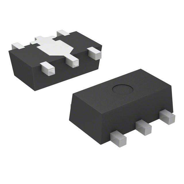
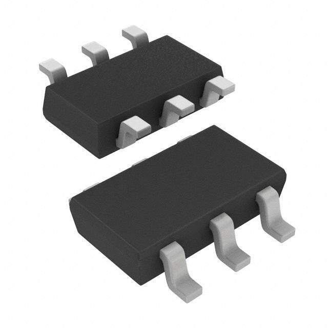
ICGOO在线商城 > 集成电路(IC) > PMIC - 稳压器 - 线性 > TPS79730MDCKREP
- 型号: TPS79730MDCKREP
- 制造商: Texas Instruments
- 库位|库存: xxxx|xxxx
- 要求:
| 数量阶梯 | 香港交货 | 国内含税 |
| +xxxx | $xxxx | ¥xxxx |
查看当月历史价格
查看今年历史价格
TPS79730MDCKREP产品简介:
ICGOO电子元器件商城为您提供TPS79730MDCKREP由Texas Instruments设计生产,在icgoo商城现货销售,并且可以通过原厂、代理商等渠道进行代购。 TPS79730MDCKREP价格参考。Texas InstrumentsTPS79730MDCKREP封装/规格:PMIC - 稳压器 - 线性, Linear Voltage Regulator IC Positive Fixed 1 Output 3V 10mA SC-70-5。您可以下载TPS79730MDCKREP参考资料、Datasheet数据手册功能说明书,资料中有TPS79730MDCKREP 详细功能的应用电路图电压和使用方法及教程。
| 参数 | 数值 |
| 产品目录 | 集成电路 (IC) |
| 描述 | IC REG LDO 3V 10MA SC70-5 |
| 产品分类 | |
| 品牌 | Texas Instruments |
| 数据手册 | |
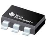
| 产品图片 |
|
| 产品型号 | TPS79730MDCKREP |
| rohs | 无铅 / 符合限制有害物质指令(RoHS)规范要求 |
| 产品系列 | - |
| 产品目录页面 | |
| 供应商器件封装 | SC-70-5 |
| 其它名称 | 296-22527-6 |
| 包装 | Digi-Reel® |
| 安装类型 | 表面贴装 |
| 封装/外壳 | 6-TSSOP(5 引线),SC-88A,SOT-353 |
| 工作温度 | -55°C ~ 125°C |
| 标准包装 | 1 |
| 电压-跌落(典型值) | 0.125V @ 10mA |
| 电压-输入 | 最高 5.5V |
| 电压-输出 | 3V |
| 电流-输出 | 10mA |
| 电流-限制(最小值) | - |
| 稳压器拓扑 | 正,固定式 |
| 稳压器数 | 1 |
| 配用 | /product-detail/zh/TPS79733EVM/296-13595-ND/486553 |



PDF Datasheet 数据手册内容提取
TPS79718-EP, TPS79730-EP, TPS79733-EP www.ti.com SGLS348A–AUGUST2006–REVISEDOCTOBER2007 ULTRA LOW-POWER, 10 mA, LDO LINEAR REGULATORS WITH POWER GOOD OUTPUT FEATURES APPLICATIONS 1 • ControlledBaseline • Battery-PoweredMicrocontrollersand Microprocessors – OneAssemblySite – OneTestSite DESCRIPTION/ORDERING INFORMATION – OneFabricationSite The TPS797xx family of low-dropout (LDO) voltage • ExtendedTemperaturePerformanceof regulators offers the benefits of low-dropout voltage –55(cid:176) Cto125(cid:176) C and ultralow-power operation. The device is stable • EnhancedDiminishingManufacturingSources with any capacitor (> 0.47 m F). Therefore, (DMS)Support implementations of this device require little board • EnhancedProduct-ChangeNotification space due to the miniaturized packaging and potentially small output capacitor. In addition, the • QualificationPedigree(1) family includes an integrated open drain active-high • 10mALow-DropoutRegulator power good (PG) output. Intended for use in • Ultralow1.2m AQuiescentCurrentat10mA microcontroller based, battery-powered applications, the TPS797xx family's low dropout and • 5-PinSC70/SOT-323(DCK)Package ultralow-powered operation results in a significant • IntegratedPowerGoodOutput increase in system battery operating life. The small • StableWithAnyCapacitor(>0.47m F) packagingminimizesconsumptionofboardspace. • DropoutVoltageTypically105mVat10mA The device is enabled when the applied voltage (TPS79733) exceeds the minimum input voltage. The usual PNP • OvercurrentLimitation pass transistor has been replaced by a PMOS pass element. Because the PMOS pass element behaves (1) ComponentqualificationinaccordancewithJEDECand as a low-value resistor, the dropout voltage is low, industrystandardstoensurereliableoperationoveran 125 mV (typ) at 10 mA of load current and is directly extendedtemperaturerange.Thisincludes,butisnotlimited proportionaltotheloadcurrent.Thequiescentcurrent to,HighlyAcceleratedStressTest(HAST)orbiased85/85, temperaturecycle,autoclaveorunbiasedHAST, is ultralow (1.2 m A typ) and is stable over the entire electromigration,bondintermetalliclife,andmoldcompound range of output load current (0 mA to 10 mA). When life.Suchqualificationtestingshouldnotbeviewedas properly configured with a pullup resistor, the PG justifyinguseofthiscomponentbeyondspecified output can be used to implement a power-on reset or performanceandenvironmentallimits. low battery indicator. The TPS797xx is offered in 1.8V,3V,and3.3Vfixedoptions. ORDERINGINFORMATION(1) T VOLTAGE PACKAGE(2) PARTNUMBER SYMBOL A 1.8V TPS79718MDCKREP CKW –55(cid:176) Cto125(cid:176) C 3V SC70/SOT-323(DCK) TPS79730MDCKREP BUA 3.3V TPS79733MDCKREP(3) TBD (1) Forthemostcurrentpackageandorderinginformation,seethePackageOptionAddendumattheendofthisdocument,orseetheTI websiteatwww.ti.com. (2) Packagedrawings,thermaldata,andsymbolizationareavailableatwww.ti.com/packaging. (3) ProductPreview.Parametersinelectricalcharacteristicsaresubjecttochange. 1 Pleasebeawarethatanimportantnoticeconcerningavailability,standardwarranty,anduseincriticalapplicationsof TexasInstrumentssemiconductorproductsanddisclaimerstheretoappearsattheendofthisdatasheet. UNLESS OTHERWISE NOTED this document contains Copyright©2006–2007,TexasInstrumentsIncorporated PRODUCTION DATA information current as of publication date. Products conform to specifications per the terms of Texas Instruments standard warranty. Production processing does not necessarilyincludetestingofallparameters.
TPS79718-EP, TPS79730-EP, TPS79733-EP www.ti.com SGLS348A–AUGUST2006–REVISEDOCTOBER2007 DCK PACKAGE GROUND CURRENT (TOP VIEW) vs FREE-AIR TEMPERATURE PG 1 5 OUT 2 VI = 4.3 V GND 2 1.75 VO = 3.3 V Co = 1 m F A IO = 10 mA NC 3 4 IN m− 1.50 nt e urr 1.25 C d n u 1 o Gr 0.75 0.50 −40 −15 10 35 60 85 TA − Free-Air Temperature − °C DEVICE INFORMATION FUNCTIONALBLOCKDIAGRAM VIN VOUT Current Sense ILIM R1 _ + GND R2 Vref = 1.235 V Bandgap VIN Reference PG Delay TERMINALFUNCTIONS TERMINAL I/O DESCRIPTION NAME NO. IN 4 I TheINterminalisthepowersupplyinputtothedevice. GND 2 Ground NC 3 Noconnection OUT 5 O TheOUTterminalprovidestheregulatedoutputvoltageofthedevice. ThePGterminalforthefixedvoltageoptiondevicesisanopen-drainactive-highoutputthatindicates thestatusofV (outputoftheLDO).WhenV exceedsapproximately90%oftheregulatedvoltage, O O PG 1 O PGgoestoahighimpedancestate.Itgoestoalow-impedancestatewhenV fallsbelow O approximately90%(i.e.overloadcondition)oftheregulatedvoltage.TheopendrainoutputofthePG terminalrequiresapullupresistor. 2 SubmitDocumentationFeedback Copyright©2006–2007,TexasInstrumentsIncorporated ProductFolderLink(s):TPS79718-EP TPS79730-EP TPS79733-EP
TPS79718-EP, TPS79730-EP, TPS79733-EP www.ti.com SGLS348A–AUGUST2006–REVISEDOCTOBER2007 ABSOLUTE MAXIMUM RATINGS(1) overoperatingfree-airtemperaturerange(unlessotherwisenoted) VALUE UNIT Inputvoltagerange(2) 0.3to6 V Maximumdcoutputvoltage 4.9 V Peakoutputcurrent Internallylimited ESDrating,HBM 3 kV ESDrating,CDM 1 kV Continuoustotalpowerdissipation SeeDissipationRatingTable T Operatingjunctiontemperaturerange –55to145 (cid:176) C J T Operatingambienttemperaturerange –55to125 (cid:176) C A T Storagetemperaturerange –65to150 (cid:176) C stg (1) Stressesbeyondthoselistedunder"absolutemaximumratings"maycausepermanentdamagetothedevice.Thesearestressratings only,andfunctionaloperationofthedeviceattheseoranyotherconditionsbeyondthoseindicatedunder"recommendedoperating conditions"isnotimplied.Exposuretoabsolute-maximum-ratedconditionsforextendedperiodsmayaffectdevicereliability. (2) Allvoltagevaluesarewithrespecttonetworkgroundterminal. DISSIPATION RATINGS DERATING T ≥25(cid:176) C T =70(cid:176) C T =85(cid:176) C T =125(cid:176) C BOARD PACKAGE ((cid:176)RCq/JWC) ((cid:176)RCq/JWA) FAABCOTVOER PAOWER PAOWER PAOWER APOWER T =25(cid:176) C RATING RATING RATING RATING A LowK DCK 165.39 396.24 2.52mW/(cid:176) C 252mW 139mW 101mW 0W HighK DCK 165.39 314.74 3.18mW/(cid:176) C 318mW 175mW 127mW 127mW Copyright©2006–2007,TexasInstrumentsIncorporated SubmitDocumentationFeedback 3 ProductFolderLink(s):TPS79718-EP TPS79730-EP TPS79733-EP
TPS79718-EP, TPS79730-EP, TPS79733-EP www.ti.com SGLS348A–AUGUST2006–REVISEDOCTOBER2007 ELECTRICAL CHARACTERISTICS overoperatingfree-airtemperaturerange(unlessotherwisenoted) PARAMETER TESTCONDITIONS MIN TYP MAX UNIT I =3mA 1.8 5.5 V V Inputvoltage(1) O I I =10mA 2 5.5 V O I Continuousoutputcurrent(2) 0 10 mA O T Operatingambienttemperature –55 125 (cid:176) C A T =25(cid:176) C,2.8V<V <5.5V 1.8 A I TPS79718 T =–55(cid:176) Cto125(cid:176) C, 1.705 1.895 V J 2.8V<V <5.5V I T =25(cid:176) C,4V<V <5.5V 3 A I Outputvoltage (1mAto10mAload)(3) TPS79730 TJ=–55(cid:176) Cto125(cid:176) C, 2.88 3.12 V 4V<V <5.5V I T =25(cid:176) C,4.3V<V <5.5V 3.3 A I TPS79733 T =–55(cid:176) Cto125(cid:176) C, 3.168 3.432 V J 4.3V<V <5.5V I T =25(cid:176) C,0mA<I <10mA 1.2 Quiescentcurrent(GNDcurrent)(3) A O m A T =–55(cid:176) Cto125(cid:176) C,I =10mA 5 J O Loadregulation T =25(cid:176) C,I =1mAto10mA 17 mV A O V +1V<V ≤5.5V,T =25(cid:176) C 0.15 O I A Outputvoltagelineregulation (ΔVout/ΔVin)(3) VO+1V<VI≤5.5V, 0.8 %/V T =–55(cid:176) Cto125(cid:176) C J Outputnoisevoltage(TPS79718) BW=200Hzto100kHz, 600 m V RMS C =10mF, O I =10mA,T =25(cid:176) C O A Outputcurrentlimit V =0V,SeeNote4 190 300 mA O Powersupplyripplerejection(TPS79718) f=100Hz,C =10mF,I =10mA, 50 dB O O T =25(cid:176) C A I =10mA,T =25(cid:176) C 125 O A TPS79730 I =10mA,T =–55(cid:176) Cto125(cid:176) C 400 Dropoutvoltage(4) O A mV I =10mA,T =25(cid:176) C 105 O A TPS79733 I =10mA,T =–55(cid:176) Cto125(cid:176) C 400 O A MinimuminputvoltageforvalidPG I =100uA,V ≥0.8V 1.2 V (PG) (PG) PGtripthresholdvoltage V decreasing 90 %V O O PGoutputlowvoltage V =1.4V,I =100uA 0.14 0.4 V I (PG) PGleakagecurrent V =5V 0.1 nA (PG) (1) Tocalculatetheminimuminputvoltageforyourmaximumoutputcurrent,usethefollowingformula:V(min)=V (max)+V (maxload) I O DO (2) Continuousoutputcurrentislimitedbyinternalprotectioncircuitry,butitisnotrecommendedthatthedeviceoperateunderconditions beyondthosespecifiedinthistableforextendedperiodsoftime. (3) TheminimumINoperatingvoltageis1.8VorV (typ)+1V,whicheverisgreater.ThemaximumINvoltageis5.5V.Thereisno O minimumoutputcurrentrequirementandthemaximumoutputcurrentis10mA. (4) INvoltageequalsV (typ)–100mV;TheTPS79730inputvoltageissetto2.9VandtheTPS79733inputvoltageissetto3.2V.The O TPS79718dropoutvoltageislimitedbyinputvoltagerangelimitations. 4 SubmitDocumentationFeedback Copyright©2006–2007,TexasInstrumentsIncorporated ProductFolderLink(s):TPS79718-EP TPS79730-EP TPS79733-EP
TPS79718-EP, TPS79730-EP, TPS79733-EP www.ti.com SGLS348A–AUGUST2006–REVISEDOCTOBER2007 TPS797xx PG TIMING DIAGRAM VIN Vmin (see Note A) t VOUT Threshold Voltage VIT+ VIT− (see Note B) (see Note B) t PG Output t A. V =V +V min OUT DO B. ThePGtripvoltageistypically10%lowerthantheoutputvoltage(90%V ).V toV isthehysteresisvoltage. O IT- IT+ Copyright©2006–2007,TexasInstrumentsIncorporated SubmitDocumentationFeedback 5 ProductFolderLink(s):TPS79718-EP TPS79730-EP TPS79733-EP
TPS79718-EP, TPS79730-EP, TPS79733-EP www.ti.com SGLS348A–AUGUST2006–REVISEDOCTOBER2007 TYPICAL CHARACTERISTICS OUTPUTVOLTAGE OUTPUTVOLTAGE OUTPUTVOLTAGE vs vs vs OUTPUTCURRENT OUTPUTCURRENT FREE-AIRTEMPERATURE 3.315 1.815 3.35 VI = 4.3 V VI = 2.8 V 3.34 VI = 4.3 V 3.310 Co = 1 m F 1.810 Co = 1 m F Co = 1 m F V TA = 25°C V TA = 25°C 3.33 − Output Voltage − O333...233900505 − Output Voltage − O111...788900505 − Output Voltage − V 33333.....2233389012 IO = IO1 m= A10 mA V V O 3.290 1.790 V 3.27 3.26 3.285 1.785 3.25 0 2 4 6 8 10 0 2 4 6 8 10 −40 −15 10 35 60 85 IO − Output Current − mA IO − Output Current − mA TA − Free-Air Temperature − °C Figure1. Figure2. Figure3. OUTPUTVOLTAGE GROUNDCURRENT OUTPUTSPECTRALNOISEDENSITY vs vs vs FREE-AIRTEMPERATURE FREE-AIRTEMPERATURE FREQUENCY 1.82 2 10 VI = 2.8 V VI = 4.3 V Hz VI = 2.8 V ut Voltage − V 11..8801 Co = 1 m FIO = 1 mA mCurrent − A 111...257505 VCIOOo = == 1 130 .m 3mF VA nV/oise Density − 68 VCOo == 11 .mI8OF V = 1 mA IO = 10 mA − OutpO 1.79 IO = 10 mA Ground 1 pectral N 4 V 0.75 ut S 2 p ut O 1.78 0.50 0 −40 −15 10 35 60 85 −40 −15 10 35 60 85 100 1 k 10 k 100 k TA − Free-Air Temperature − °C TA − Free-Air Temperature − °C f − Frequency − Hz Figure4. Figure5. Figure6. OUTPUTIMPEDANCE DROPOUTVOLTAGE vs vs vs FREQUENCY FREE-AIRTEMPERATURE POWERUP/POWERDOWN 40 140 7 W− Output Impedance − 123132055500 VVCTJIOo = === 4 213.5 3.m°3 CFV V IO = IO1 m= A10 mA − Dropout Voltage − mVO 110246800000 VCIo == 31. 2m FV IO = 10 mA V − Output Voltage − VOV− Input Voltage − VI 316524 VROL == 333.30 VW VO VI Zo 5 VD 20 IO = 1 mA 0 0 0 10 100 1k 10k 100k 1 M 10 M −40 −25 −10 5 20 35 50 65 80 0 10 20 30 40 50 60 70 80 90 100 f − Frequency − Hz TA − Free-Air Temperature − °C t − Time − ms Figure7. Figure8. Figure9. 6 SubmitDocumentationFeedback Copyright©2006–2007,TexasInstrumentsIncorporated ProductFolderLink(s):TPS79718-EP TPS79730-EP TPS79733-EP
TPS79718-EP, TPS79730-EP, TPS79733-EP www.ti.com SGLS348A–AUGUST2006–REVISEDOCTOBER2007 TYPICAL CHARACTERISTICS (continued) TPS79718 TPS79718 TPS79733 LINETRANSIENTRESPONSE LOADTRANSIENTRESPONSE LINETRANSIENTRESPONSE − Output Voltage − mVV− Input Voltage − VOI−11230550..8080000 IVCOOo = ==d d 1 vt410..7 8m= mVAF0.1m4s V D − Change InVOCurrent Load − mA Output Voltage − mV−1−110505050000000 200400 600800 1 k 12VVCIOo = =11= 24 4m1..8.7A8 1 V m6VF 18 2 k − Output Voltage − mVV− Input Voltage − VOI−−1212540000..00330000 100 200 300400 50060ICO0o dd ==v7t 10400.=7 8m 0mA00F.1m94s0 V0 1 k V 0 100 200300400500600700800900 1 k t − Time − m s V t − Time − m s t − Time − m s Figure10. Figure11. Figure12. TPS79733 LOADTRANSIENTRESPONSE VI = 4.3 V Co = 4.7 m F 100 V n m urrent − mA10 −50−051000D − Change IVO Output Voltage − C put 5 1 mA Out 0 − O I 0 200400 600800 1 k12 14 16 18 2 k t − Time − m s Figure13. Copyright©2006–2007,TexasInstrumentsIncorporated SubmitDocumentationFeedback 7 ProductFolderLink(s):TPS79718-EP TPS79730-EP TPS79733-EP
TPS79718-EP, TPS79730-EP, TPS79733-EP www.ti.com SGLS348A–AUGUST2006–REVISEDOCTOBER2007 APPLICATION INFORMATION The TPS797xx family of low-dropout (LDO) regulators haS been optimized for use in micropower applications. Thedevicesfeatureextremelylowdropoutvoltagesandultralowquiescentcurrent(1.2m Atyp). AtypicalapplicationcircuitisshowninFigure14. TPS797xx 4 IN 1 PG 100 kW 5 + C1 OUT VO 0.1 m F 3 NC − + GND 0.47 m F 2 Figure14.TypicalApplicationCircuit ExternalCapacitorRequirements Although not required, a 0.1 m F or larger input bypass capacitor, connected between IN and GND and located close to the TPS797xx, is recommended, especially when a highly resistive power supply is powering the LDO in additiontootherdevices. Like all low-dropout regulators, the TPS797xx requires an output capacitor connected between OUT and GND to stabilize the internal control loop. The minimum recommended capacitance is 0.47 m F. Any 0.47 m F capacitor is suitable.Capacitorvalueslargerthan0.47m Fareacceptable. PowerDissipationandJunctionTemperature Specified regulator operation is assured to a junction temperature of 125(cid:176) C; restrict the maximum junction temperature to 125(cid:176) C under normal operating conditions. This restriction limits the power dissipation the regulator can handle in any given application. To ensure the junction temperature is within acceptable limits, calculate the maximum allowable dissipation, P , and the actual dissipation, P , which must be less than or D(max) D equaltoP . D(max) T max(cid:1)T P (cid:2) J A Themaximum-power-dissipationlimitisdeterminedusingthefollowingequation: D(max) Rq JA Where: T maxisthemaximumallowablejunctiontemperature. J Rq JAisthethermalresistancejunction-to-ambientforthepackage(seethePowerDissipationRatingTable). TAistheambienttemperature. Theregulatordissipationiscalculatedusing: P =(V -V )· I D I O O Power dissipation resulting from quiescent current is negligible. Excessive power dissipation triggers the thermal protectioncircuit. 8 SubmitDocumentationFeedback Copyright©2006–2007,TexasInstrumentsIncorporated ProductFolderLink(s):TPS79718-EP TPS79730-EP TPS79733-EP
TPS79718-EP, TPS79730-EP, TPS79733-EP www.ti.com SGLS348A–AUGUST2006–REVISEDOCTOBER2007 RegulatorProtection The TPS797xx PMOS-pass transistor has a built-in back diode that conducts reverse current when the input voltage drops below the output voltage (e.g., during power down). Current is conducted from the output to the input and is not internally limited. If extended reverse voltage operation is anticipated, external limiting might be appropriate. The TPS797xx features internal current limiting. During normal operation, the TPS797xx limits output current to approximately 190 mA. When current limiting engages, the output voltage scales back linearly until the overcurrentconditionends.Takecarenottoexceedthepowerdissipationratingsofthepackage. MicrocontrollerApplication One application for which this device is particularly suited is providing a regulated input voltage and power good (PG) supervisory signal to low-power devices such as mixed-signal microcontrollers. The quiescent or ground current of the TPS797xx family is typically 1.2 m A even at full load; therefore, the reduction in battery life by including the TPS797xx in the system is negligible. The primary benefits of using the TPS797xx to power low powerdigitaldevicesinclude: • Regulated output voltage that protects the device from battery droop and noise on the line (e.g., switch bounce) • Smooth,monotonicpowerup • PGsignalforcontrolleddeviceRESET • Potentialtouseanexisting5-Vpowerrailtopowera3.3Vorlowerdevice • Potential to provide separate digital and analog power and ground supplies for a system with only one power source Figure 15 shows an application in which the TPS79718 is used to power Texas Instruments MSP430 mixed signalmicrocontroller. VIN VOUT VCC 1.8 V + 0.47 m F MSP430 TPS79718 or Equivalent − 0.1 m F PG RESET GND VSS Figure15.MSP430MicrocontrollerPoweredbytheTPS79718Regulator Minimal board space is needed to accommodate the DCK (SC70/SOT-323) packaged TPS79718, the 0.1 m F outputcapacitor,the0.47m Finputcapacitor,andthepullupresistoronthePGpin. Copyright©2006–2007,TexasInstrumentsIncorporated SubmitDocumentationFeedback 9 ProductFolderLink(s):TPS79718-EP TPS79730-EP TPS79733-EP
PACKAGE OPTION ADDENDUM www.ti.com 6-Feb-2020 PACKAGING INFORMATION Orderable Device Status Package Type Package Pins Package Eco Plan Lead/Ball Finish MSL Peak Temp Op Temp (°C) Device Marking Samples (1) Drawing Qty (2) (6) (3) (4/5) TPS79718MDCKREP ACTIVE SC70 DCK 5 3000 Green (RoHS NIPDAUAG Level-1-260C-UNLIM -55 to 125 CKW & no Sb/Br) TPS79730MDCKREP ACTIVE SC70 DCK 5 3000 Green (RoHS NIPDAUAG Level-1-260C-UNLIM -55 to 125 BUA & no Sb/Br) V62/06673-01XE ACTIVE SC70 DCK 5 3000 Green (RoHS NIPDAUAG Level-1-260C-UNLIM -55 to 125 CKW & no Sb/Br) V62/06673-02XE ACTIVE SC70 DCK 5 3000 Green (RoHS NIPDAUAG Level-1-260C-UNLIM -55 to 125 BUA & no Sb/Br) (1) The marketing status values are defined as follows: ACTIVE: Product device recommended for new designs. LIFEBUY: TI has announced that the device will be discontinued, and a lifetime-buy period is in effect. NRND: Not recommended for new designs. Device is in production to support existing customers, but TI does not recommend using this part in a new design. PREVIEW: Device has been announced but is not in production. Samples may or may not be available. OBSOLETE: TI has discontinued the production of the device. (2) RoHS: TI defines "RoHS" to mean semiconductor products that are compliant with the current EU RoHS requirements for all 10 RoHS substances, including the requirement that RoHS substance do not exceed 0.1% by weight in homogeneous materials. Where designed to be soldered at high temperatures, "RoHS" products are suitable for use in specified lead-free processes. TI may reference these types of products as "Pb-Free". RoHS Exempt: TI defines "RoHS Exempt" to mean products that contain lead but are compliant with EU RoHS pursuant to a specific EU RoHS exemption. Green: TI defines "Green" to mean the content of Chlorine (Cl) and Bromine (Br) based flame retardants meet JS709B low halogen requirements of <=1000ppm threshold. Antimony trioxide based flame retardants must also meet the <=1000ppm threshold requirement. (3) MSL, Peak Temp. - The Moisture Sensitivity Level rating according to the JEDEC industry standard classifications, and peak solder temperature. (4) There may be additional marking, which relates to the logo, the lot trace code information, or the environmental category on the device. (5) Multiple Device Markings will be inside parentheses. Only one Device Marking contained in parentheses and separated by a "~" will appear on a device. If a line is indented then it is a continuation of the previous line and the two combined represent the entire Device Marking for that device. (6) Lead/Ball Finish - Orderable Devices may have multiple material finish options. Finish options are separated by a vertical ruled line. Lead/Ball Finish values may wrap to two lines if the finish value exceeds the maximum column width. Important Information and Disclaimer:The information provided on this page represents TI's knowledge and belief as of the date that it is provided. TI bases its knowledge and belief on information provided by third parties, and makes no representation or warranty as to the accuracy of such information. Efforts are underway to better integrate information from third parties. TI has taken and Addendum-Page 1
PACKAGE OPTION ADDENDUM www.ti.com 6-Feb-2020 continues to take reasonable steps to provide representative and accurate information but may not have conducted destructive testing or chemical analysis on incoming materials and chemicals. TI and TI suppliers consider certain information to be proprietary, and thus CAS numbers and other limited information may not be available for release. In no event shall TI's liability arising out of such information exceed the total purchase price of the TI part(s) at issue in this document sold by TI to Customer on an annual basis. Addendum-Page 2
PACKAGE MATERIALS INFORMATION www.ti.com 3-Aug-2017 TAPE AND REEL INFORMATION *Alldimensionsarenominal Device Package Package Pins SPQ Reel Reel A0 B0 K0 P1 W Pin1 Type Drawing Diameter Width (mm) (mm) (mm) (mm) (mm) Quadrant (mm) W1(mm) TPS79718MDCKREP SC70 DCK 5 3000 180.0 8.4 2.41 2.41 1.2 4.0 8.0 Q3 TPS79730MDCKREP SC70 DCK 5 3000 180.0 8.4 2.41 2.41 1.2 4.0 8.0 Q3 PackMaterials-Page1
PACKAGE MATERIALS INFORMATION www.ti.com 3-Aug-2017 *Alldimensionsarenominal Device PackageType PackageDrawing Pins SPQ Length(mm) Width(mm) Height(mm) TPS79718MDCKREP SC70 DCK 5 3000 202.0 201.0 28.0 TPS79730MDCKREP SC70 DCK 5 3000 202.0 201.0 28.0 PackMaterials-Page2
None
None
IMPORTANTNOTICEANDDISCLAIMER TI PROVIDES TECHNICAL AND RELIABILITY DATA (INCLUDING DATASHEETS), DESIGN RESOURCES (INCLUDING REFERENCE DESIGNS), APPLICATION OR OTHER DESIGN ADVICE, WEB TOOLS, SAFETY INFORMATION, AND OTHER RESOURCES “AS IS” AND WITH ALL FAULTS, AND DISCLAIMS ALL WARRANTIES, EXPRESS AND IMPLIED, INCLUDING WITHOUT LIMITATION ANY IMPLIED WARRANTIES OF MERCHANTABILITY, FITNESS FOR A PARTICULAR PURPOSE OR NON-INFRINGEMENT OF THIRD PARTY INTELLECTUAL PROPERTY RIGHTS. These resources are intended for skilled developers designing with TI products. You are solely responsible for (1) selecting the appropriate TI products for your application, (2) designing, validating and testing your application, and (3) ensuring your application meets applicable standards, and any other safety, security, or other requirements. These resources are subject to change without notice. TI grants you permission to use these resources only for development of an application that uses the TI products described in the resource. Other reproduction and display of these resources is prohibited. No license is granted to any other TI intellectual property right or to any third party intellectual property right. TI disclaims responsibility for, and you will fully indemnify TI and its representatives against, any claims, damages, costs, losses, and liabilities arising out of your use of these resources. TI’s products are provided subject to TI’s Terms of Sale (www.ti.com/legal/termsofsale.html) or other applicable terms available either on ti.com or provided in conjunction with such TI products. TI’s provision of these resources does not expand or otherwise alter TI’s applicable warranties or warranty disclaimers for TI products. Mailing Address: Texas Instruments, Post Office Box 655303, Dallas, Texas 75265 Copyright © 2020, Texas Instruments Incorporated
 Datasheet下载

