ICGOO在线商城 > TPS76533D

 Datasheet下载
- 型号: TPS76533D
- 制造商: Texas Instruments
- 库位|库存: xxxx|xxxx
- 要求:
| 数量阶梯 | 香港交货 | 国内含税 |
| +xxxx | $xxxx | ¥xxxx |
查看当月历史价格
查看今年历史价格
TPS76533D产品简介:
ICGOO电子元器件商城为您提供TPS76533D由Texas Instruments设计生产,在icgoo商城现货销售,并且可以通过原厂、代理商等渠道进行代购。 提供TPS76533D价格参考¥5.38-¥5.38以及Texas InstrumentsTPS76533D封装/规格参数等产品信息。 你可以下载TPS76533D参考资料、Datasheet数据手册功能说明书, 资料中有TPS76533D详细功能的应用电路图电压和使用方法及教程。
| 参数 | 数值 |
| 产品目录 | 集成电路 (IC)半导体 |
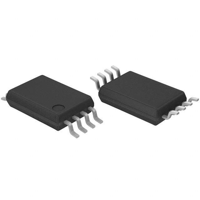
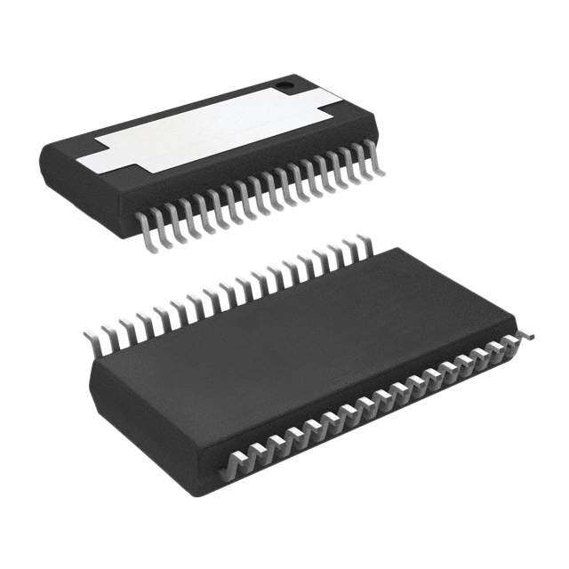
| 描述 | IC REG LDO 3.3V 0.15A 8SOIC低压差稳压器 150mA 3.3V LDO |
| 产品分类 | |
| 品牌 | Texas Instruments |
| 产品手册 | |
| 产品图片 |
|
| rohs | 符合RoHS无铅 / 符合限制有害物质指令(RoHS)规范要求 |
| 产品系列 | 电源管理 IC,低压差稳压器,Texas Instruments TPS76533D- |
| 数据手册 | |
| 产品型号 | TPS76533D |
| 产品目录页面 | |
| 产品种类 | 低压差稳压器 |
| 供应商器件封装 | 8-SOIC |
| 其它名称 | 296-2720-5 |
| 包装 | 管件 |
| 单位重量 | 76 mg |
| 商标 | Texas Instruments |
| 回动电压—最大值 | 240 mV |
| 安装类型 | 表面贴装 |
| 安装风格 | SMD/SMT |
| 封装 | Tube |
| 封装/外壳 | 8-SOIC(0.154",3.90mm 宽) |
| 封装/箱体 | SOIC-8 |
| 工作温度 | -40°C ~ 125°C |
| 工厂包装数量 | 75 |
| 最大功率耗散 | 0.904 W |
| 最大工作温度 | + 125 C |
| 最大输入电压 | 10 V |
| 最小工作温度 | - 40 C |
| 最小输入电压 | + 2.7 V |
| 标准包装 | 75 |
| 电压-跌落(典型值) | 0.14V @ 150mA |
| 电压-输入 | 最高 10V |
| 电压-输出 | 3.3V |
| 电压调节准确度 | 3 % |
| 电流-输出 | 150mA |
| 电流-限制(最小值) | - |
| 稳压器拓扑 | 正,固定式 |
| 稳压器数 | 1 |
| 系列 | TPS76533 |
| 线路调整率 | 0.01 % / V |
| 负载调节 | 0.3 % |
| 输入偏压电流—最大 | 0.035 mA |
| 输出电压 | 3.3 V |
| 输出电流 | 150 mA |
| 输出端数量 | 1 Output |
| 输出类型 | Fixed |


- 商务部:美国ITC正式对集成电路等产品启动337调查
- 曝三星4nm工艺存在良率问题 高通将骁龙8 Gen1或转产台积电
- 太阳诱电将投资9.5亿元在常州建新厂生产MLCC 预计2023年完工
- 英特尔发布欧洲新工厂建设计划 深化IDM 2.0 战略
- 台积电先进制程称霸业界 有大客户加持明年业绩稳了
- 达到5530亿美元!SIA预计今年全球半导体销售额将创下新高
- 英特尔拟将自动驾驶子公司Mobileye上市 估值或超500亿美元
- 三星加码芯片和SET,合并消费电子和移动部门,撤换高东真等 CEO
- 三星电子宣布重大人事变动 还合并消费电子和移动部门
- 海关总署:前11个月进口集成电路产品价值2.52万亿元 增长14.8%

PDF Datasheet 数据手册内容提取
Obsolete Devices: TPS76501, TPS76525, TPS76528 TPS76515, TPS76518, TPS76525, TPS76527 TPS76528, TPS76530, TPS76533, TPS76550, TPS76501 ULTRA-LOW QUIESCIENT CURRENT 150-mA LOW-DROPOUT VOLTAGE REGULATORS SLVS236 – AUGUST 1999 (cid:0) 150-mA Low-Dropout Voltage Regulator D PACKAGE (cid:0) (TOP VIEW) Available in 1.5-V, 1.8-V, 2.5-V, 2.7-V, 2.8-V, 3.0-V, 3.3-V, 5.0-V Fixed Output and NC/FB 1 8 OUT Adjustable Versions PG 2 7 OUT (cid:0) Dropout Voltage to 85 mV (Typ) at 150 mA GND 3 6 IN (TPS76550) EN 4 5 IN (cid:0) Ultra-Low 35-m A Typical Quiescent Current (cid:0) 3% Tolerance Over Specified Conditions for Fixed-Output Versions (cid:0) Open Drain Power Good (cid:0) 8-Pin SOIC Package (cid:0) Thermal Shutdown Protection description This device is designed to have an ultra-low quiescent current and be stable with a 4.7-m F capacitor. This combination provides high performance at a reasonable cost. Because the PMOS device behaves as a low-value resistor, the dropout voltage is very low (typically 85 mV at an output current of 150 mA for the TPS76550) and is directly proportional to the output current. Additionally, since the PMOS pass element is a voltage-driven device, the quiescent current is very low and independent of output loading (typically 35 m A over the full range of output current, 0 mA to 150 mA). These two key specifications yield a significant improvement in operating life for battery-powered systems. This LDO family also features a sleep mode; applying a TTL high signal to EN (enable) shuts down the regulator, reducing the quiescent current to less than 1 m A (typ). TPS76533 TPS76533 DROPOUT VOLTAGE GROUND CURRENT vs vs FREE-AIR TEMPERATURE LOAD CURRENT 10100 35.0 VI = 3.2 V VO = 3.3 V 34.9 TA = 25°C 34.8 A e – V 10–1 IO = 150 mA mnt – 34.7 g e Volta IO = 50 mA Curr 34.6 ut nd 34.5 p u Out IO = 10 mA Gro 34.4 – 10–2 – O D 34.3 D N V G I 34.2 34.1 10–31 34.0 –50 –25 0 25 50 75 100 125 150 0 25 50 75 100 125 150 TA – Free-Air Temperature – °C IL – Load Current – mA Please be aware that an important notice concerning availability, standard warranty, and use in critical applications of TexasInstruments semiconductor products and disclaimers thereto appears at the end of this data sheet. PRODUCTION DATA information is current as of publication date. Copyright 1999, Texas Instruments Incorporated Products conform to specifications per the terms of Texas Instruments standard warranty. Production processing does not necessarily include testing of all parameters. POST OFFICE BOX 655303 • DALLAS, TEXAS 75265 1
Obsolete Devices: TPS76501, TPS76525, TPS76528 TPS76515, TPS76518, TPS76525, TPS76527 TPS76528, TPS76530, TPS76533, TPS76550, TPS76501 ULTRA-LOW QUIESCIENT CURRENT 150-mA LOW-DROPOUT VOLTAGE REGULATORS SLVS236 – AUGUST 1999 description (continued) Power good (PG) is an active high output, which can be used to implement a power-on reset or a low-battery indicator. The TPS765xx is offered in 1.5-V, 1.8-V, 2.5-V, 2.7-V, 2.8-V, 3.0-V, 3.3-V and 5.0-V fixed-voltage versions and in an adjustable version (programmable over the range of 1.25 V to 5.5 V). Output voltage tolerance is specified as a maximum of 3% over line, load, and temperature ranges. The TPS765xx family is available in 8 pin SOIC package. AVAILABLE OPTIONS OUTPUT VOLTAGE PACKAGED DEVICES (V) TTJJ SOIC TYP (D) 5.0 TPS76550D 3.3 TPS76533D 3.0 TPS76530D 2.8 TPS76528D 2.7 TPS76527D ––4400°CC ttoo 112255°CC 2.5 TPS76525D 1.8 TPS76518D 1.5 TPS76515D Adjustable TPS76501D 1.25 V to 5.5 V The TPS76501 is programmable using an external resistor divider (see application information). The D package is available taped and reeled. Add an R suffix to the device type (e.g., TPS76501DR). TPS765xx 5 2 VI IN PG PG 6 1 IN NC/FB 7 OUT VO 0.1 m F 4 8 EN OUT CO† + 4.7 m F GND 3 300 mW †See application information section for capacitor selection details. Figure 1. Typical Application Configuration for Fixed Output Options 2 POST OFFICE BOX 655303 • DALLAS, TEXAS 75265
Obsolete Devices: TPS76501, TPS76525, TPS76528 TPS76515, TPS76518, TPS76525, TPS76527 TPS76528, TPS76530, TPS76533, TPS76550, TPS76501 ULTRA-LOW QUIESCIENT CURRENT 150-mA LOW-DROPOUT VOLTAGE REGULATORS SLVS236 – AUGUST 1999 functional block diagram—adjustable version IN EN PG _ + OUT + R1 _ Vref = 1.224 V FB/NC R2 GND External to the device functional block diagram—fixed-voltage version IN EN PG _ + OUT + _ R1 Vref = 1.224 V R2 GND POST OFFICE BOX 655303 • DALLAS, TEXAS 75265 3
Obsolete Devices: TPS76501, TPS76525, TPS76528 TPS76515, TPS76518, TPS76525, TPS76527 TPS76528, TPS76530, TPS76533, TPS76550, TPS76501 ULTRA-LOW QUIESCIENT CURRENT 150-mA LOW-DROPOUT VOLTAGE REGULATORS SLVS236 – AUGUST 1999 Terminal Functions – SOIC Package TERMINAL II//OO DDEESSCCRRIIPPTTIIOONN NAME NO. EN 4 I Enable input FB/NC 1 I Feedback input voltage for adjustable device (no connect for fixed options) GND 3 Regulator ground IN 5 I Input voltage IN 6 I Input voltage OUT 7 O Regulated output voltage OUT 8 O Regulated output voltage PG 2 O PG output absolute maximum ratings over operating free-air temperature range (unless otherwise noted)(cid:0) Input voltage range‡, V . . . . . . . . . . . . . . . . . . . . . . . . . . . . . . . . . . . . . . . . . . . . . . . . . . . . . . . . . . –0.3 V to 13.5 V I Voltage range at EN . . . . . . . . . . . . . . . . . . . . . . . . . . . . . . . . . . . . . . . . . . . . . . . . . . . . . . . . . . . . . . –0.3 V to 16.5 V Maximum PG voltage . . . . . . . . . . . . . . . . . . . . . . . . . . . . . . . . . . . . . . . . . . . . . . . . . . . . . . . . . . . . . . . . . . . . . 16.5 V Peak output current . . . . . . . . . . . . . . . . . . . . . . . . . . . . . . . . . . . . . . . . . . . . . . . . . . . . . . . . . . . . . . Internally limited Continuous total power dissipation . . . . . . . . . . . . . . . . . . . . . . . . . . . . . . . . . . . . . . See dissipation rating tables Output voltage, V (OUT, FB) . . . . . . . . . . . . . . . . . . . . . . . . . . . . . . . . . . . . . . . . . . . . . . . . . . . . . . . . . . . . . . . . 7 V O Operating virtual junction temperature range, T . . . . . . . . . . . . . . . . . . . . . . . . . . . . . . . . . . . . . –40°C to 125°C J Storage temperature range, T . . . . . . . . . . . . . . . . . . . . . . . . . . . . . . . . . . . . . . . . . . . . . . . . . . . –65°C to 150°C stg ESD rating, HBM . . . . . . . . . . . . . . . . . . . . . . . . . . . . . . . . . . . . . . . . . . . . . . . . . . . . . . . . . . . . . . . . . . . . . . . . . . 2 kV †Stresses beyond those listed under “absolute maximum ratings” may cause permanent damage to the device. These are stress ratings only, and functional operation of the device at these or any other conditions beyond those indicated under “recommended operating conditions” is not implied. Exposure to absolute-maximum-rated conditions for extended periods may affect device reliability. ‡All voltage values are with respect to network terminal ground. DISSIPATION RATING TABLE 1 – FREE-AIR TEMPERATURES AIR FLOW TA < 25°C DERATING FACTOR TA = 70°C TA = 85°C PACKAGE (CFM) POWER RATING ABOVE TA = 25°C POWER RATING POWER RATING 0 568 mW 5.68 mW/°C 312 mW 227 mW DD 250 904 mW 9.04 mW/°C 497 mW 361 mW recommended operating conditions MIN MAX UNIT Input voltage, VI(cid:0) 2.7 10 V Output voltage range, VO 1.2 5.5 V Output current, IO (Note 1) 0 150 mA Operating virtual junction temperature, TJ (Note 1) –40 125 °C (cid:0) To calculate the minimum input voltage for your maximum output current, use the following equation: VI(min) = VO(max) + VDO(max load). NOTE 1: Continuous current and operating junction temperature are limited by internal protection circuitry, but it is not recommended that the device operate under conditions beyond those specified in this table for extended periods of time. 4 POST OFFICE BOX 655303 • DALLAS, TEXAS 75265
Obsolete Devices: TPS76501, TPS76525, TPS76528 TPS76515, TPS76518, TPS76525, TPS76527 TPS76528, TPS76530, TPS76533, TPS76550, TPS76501 ULTRA-LOW QUIESCIENT CURRENT 150-mA LOW-DROPOUT VOLTAGE REGULATORS SLVS236 – AUGUST 1999 electrical characteristics over recommended operating free-air temperature range, Vi = VO(typ) + 1 V, IO = 10 m A, EN = 0 V, CO = 4.7 m F (unless otherwise noted) PARAMETER TEST CONDITIONS MIN TYP MAX UNIT 5.5 V ≥ VO ≥ 1.25 V, TJ = 25°C VO TTPPSS7766550011 5.5 V ≥ VO ≥ 1.25 V, TJ = –40°C to 125°C 0.97VO 1.03VO TJ = 25°C, 2.7 V < VIN < 10 V 1.5 TTPPSS7766551155 TJ = –40°C to 125°C, 2.7 V < VIN < 10 V 1.455 1.545 TJ = 25°C, 2.8 V < VIN < 10 V 1.8 TTPPSS7766551188 TJ = –40°C to 125°C, 2.8 V < VIN < 10 V 1.746 1.854 TJ = 25°C, 3.5 V < VIN < 10 V 2.5 TTPPSS7766552255 TJ = –40°C to 125°C, 3.5 V < VIN < 10 V 2.425 2.575 Output voltage TJ = 25°C, 3.7 V < VIN < 10 V 2.7 ((1100 mm AA ttoo 115500 mmAA llooaadd)) TTPPSS7766552277 VV ((sseeee NNoottee 22)) TJ = –40°C to 125°C, 3.7 V < VIN < 10 V 2.619 2.781 TJ = 25°C, 3.8 V < VIN < 10 V 2.8 TTPPSS7766552288 TJ = –40°C to 125°C, 3.8 V < VIN < 10 V 2.716 2.884 TJ = 25°C, 4.0 V < VIN < 10 V 3.0 TTPPSS7766553300 TJ = –40°C to 125°C, 4.0 V < VIN < 10 V 2.910 3.090 TJ = 25°C, 4.3 V < VIN < 10 V 3.3 TTPPSS7766553333 TJ = –40°C to 125°C, 4.3 V < VIN < 10 V 3.201 3.399 TJ = 25°C, 6.0 V < VIN < 10 V 5.0 TTPPSS7766555500 TJ = –40°C to 125°C, 6.0 V < VIN < 10 V 4.850 5.150 Quiescent current ((GND current)) 10 m A < IO < 150 mA, TJ = 25°C 35 mm AA EN = 0V, (see Note 2) IO = 150 mA, TJ = –40°C to 125°C 50 O(suetep uNto vtoelsta 2g aen lidn e3 )regulation (D VO/VO) VO + 1 V < VI ≤ 10 V, TJ = 25°C 0.01 %/V Load regulation IO = 10 m A to 150 mA 0.3% BW = 300 Hz to 50 kHz, Output noise voltage 200 m Vrms CO = 4.7 m F, TJ = 25°C Output current Limit VO = 0 V 0.8 1.2 A Thermal shutdown junction temperature 150 °C EN = VI, TJ = 25°C, 1 m A 2.7 V < VI < 10 V SSttaannddbbyy ccuurrrreenntt EN = VI, TJ = –40°C to 125°C 10 m A 2.7 V < VI < 10 V FB input current TPS76501 FB = 1.5 V 2 nA High level enable input voltage 2.0 V Low level enable input voltage 0.8 V f = 1 kHz, CO = 4.7 m F, Power supply ripple rejection (see Note 2) 63 dB IO = 10 m A, TJ = 25°C Minimum input voltage for valid PG IO(PG) = 300m A 1.1 V Trip threshold voltage VO decreasing 92 98 %VO PG Hysteresis voltage Measured at VO 0.5 %VO Output low voltage VI = 2.7 V, IO(PG) = 1mA 0.15 0.4 V Leakage current V(PG) = 5 V 1 m A EN = 0 V –1 0 1 IInnppuutt ccuurrrreenntt ((EENN)) mm AA EN = VI –1 1 NOTE: 2. Minimum IN operating voltage is 2.7 V or VO(typ) + 1 V, whichever is greater. Maximum IN voltage 10 V. POST OFFICE BOX 655303 • DALLAS, TEXAS 75265 5
Obsolete Devices: TPS76501, TPS76525, TPS76528 TPS76515, TPS76518, TPS76525, TPS76527 TPS76528, TPS76530, TPS76533, TPS76550, TPS76501 ULTRA-LOW QUIESCIENT CURRENT 150-mA LOW-DROPOUT VOLTAGE REGULATORS SLVS236 – AUGUST 1999 electrical characteristics over recommended operating free-air temperature range, Vi = VO(typ) + 1 V, IO = 10 m A, EN = 0 V, CO = 4.7 m F (unless otherwise noted) (continued) PARAMETER TEST CONDITIONS MIN TYP MAX UNIT IO = 150 mA, TJ = 25°C 190 TTPPSS7766552288 IO = 150 mA, TJ = –40°C to 125°C 330 IO = 150 mA, TJ = 25°C 160 TTPPSS7766553300 Dropout voltagge IO = 150 mA, TJ = –40°C to 125°C 280 mmVV (See Note 4) IO = 150 mA, TJ = 25°C 140 TTPPSS7766553333 IO = 150 mA, TJ = –40°C to 125°C 240 IO = 150 mA, TJ = 25°C 85 TTPPSS7766555500 IO = 150 mA, TJ = –40°C to 125°C 150 NOTES: 3. If VO ≤ 1.8 V then Vimin = 2.7 V, Vimax = 10 V: VO(cid:5)Vimax(cid:2)2.7 V(cid:6) Line Reg. (mV) (cid:3) (cid:5)%(cid:4)V(cid:6) (cid:0) (cid:0)1000 100 If VO ≥ 2.5 V then Vimin = VO + 1 V, Vimax = 10 V: VO(cid:5)Vimax(cid:2)(cid:5)VO(cid:1)1 V(cid:6)(cid:6) Line Reg. (mV) (cid:3) (cid:5)%(cid:4)V(cid:6) (cid:0) (cid:0)1000 100 4. IN voltage equals VO(Typ) – 100 mV; TPS76501 output voltage set to 3.3 V nominal with external resistor divider. TPS76515, TPS76518, TPS76525, and TPS76527 dropout voltage limited by input voltage range limitations (i.e., TPS76530 input voltage needs to drop to 2.9 V for purpose of this test). Table of Graphs FIGURE vs Load current 2, 3 OOuuttppuutt vvoollttaaggee vs Free-air temperature 4, 5 vs Load current 6, 7 GGrroouunndd ccuurrrreenntt vs Free-air temperature 8, 9 Power supply ripple rejection vs Frequency 10 Output spectral noise density vs Frequency 11 Output impedance vs Frequency 12 Dropout voltage vs Free-air temperature 13, 14 Line transient response 15, 17 Load transient response 16, 18 Output voltage vs Time 19 Dropout voltage vs Input voltage 20 Equivalent series resistance (ESR) vs Output current 21 – 24 Equivalent series resistance (ESR) vs Added ceramic capacitance 25, 26 6 POST OFFICE BOX 655303 • DALLAS, TEXAS 75265
Obsolete Devices: TPS76501, TPS76525, TPS76528 TPS76515, TPS76518, TPS76525, TPS76527 TPS76528, TPS76530, TPS76533, TPS76550, TPS76501 ULTRA-LOW QUIESCIENT CURRENT 150-mA LOW-DROPOUT VOLTAGE REGULATORS SLVS236 – AUGUST 1999 TYPICAL CHARACTERISTICS TPS76533 TPS76515 OUTPUT VOLTAGE OUTPUT VOLTAGE vs vs LOAD CURRENT LOAD CURRENT 3.304 1.494 VI = 4.3 V VI = 2.7 V TA = 25°C TA = 25°C 1.493 3.302 1.492 V V – 3.300 – e e g g a a 1.491 Volt 3.298 Volt ut ut 1.490 p p ut ut O 3.296 O – O – O 1.489 V V 3.294 1.488 3.292 1.487 0 25 50 75 100 125 150 0 25 50 75 100 125 150 IL – Load Current – mA IL – Load Current – mA Figure 2 Figure 3 TPS76533 TPS76515 OUTPUT VOLTAGE OUTPUT VOLTAGE vs vs FREE-AIR TEMPERATURE FREE-AIR TEMPERATURE 3.310 1.505 3.305 VI = 4.3 V IO = 10 m A VI = 2.7 V IO = 10 m A 1.500 3.300 V V e – 3.295 e – 1.495 IO = 150 mA g g olta 3.290 IO = 150 mA olta V V 1.490 ut ut p 3.285 p ut ut O O – 3.280 – 1.485 O O V V 3.275 1.480 3.270 3.265 1.475 –50 –25 0 25 50 75 100 125 150 –50 –25 0 25 50 75 100 125 150 TA – Free-Air Temperature – °C TA – Free-Air Temperature – °C Figure 4 Figure 5 POST OFFICE BOX 655303 • DALLAS, TEXAS 75265 7
Obsolete Devices: TPS76501, TPS76525, TPS76528 TPS76515, TPS76518, TPS76525, TPS76527 TPS76528, TPS76530, TPS76533, TPS76550, TPS76501 ULTRA-LOW QUIESCIENT CURRENT 150-mA LOW-DROPOUT VOLTAGE REGULATORS SLVS236 – AUGUST 1999 TYPICAL CHARACTERISTICS TPS76533 TPS76515 GROUND CURRENT GROUND CURRENT vs vs LOAD CURRENT LOAD CURRENT 35.0 34.0 VO = 3.3 V 34.9 TA = 25°C 33.9 VO = 1.5 V TA = 25°C 34.8 33.8 A A m– 34.7 m– 33.7 nt nt e e rr 34.6 rr 33.6 u u C C d 34.5 d 33.5 n n u u o o r 34.4 r 33.4 G G – – D 34.3 D 33.3 N N G G I 34.2 I 33.2 34.1 33.1 34.0 33.0 0 25 50 75 100 125 150 0 25 50 75 100 125 150 IL – Load Current – mA IL – Load Current – mA Figure 6 Figure 7 TPS76533 TPS76515 GROUND CURRENT GROUND CURRENT vs vs FREE-AIR TEMPERATURE FREE-AIR TEMPERATURE 55 55 50 50 A 45 A 45 m– m– nt 40 nt e e 40 r r r r Cu 35 Cu d d 35 n n u 30 u o o r r G G 30 – 25 – D D GN 20 GN 25 I I 15 VO = 3.3 V 20 VO = 1.5 V IO = 150 mA IO = 150 mA 10 15 –50 0 50 100 150 –50 0 50 100 150 TA – Free-Air Temperature – °C TA – Free-Air Temperature – °C Figure 8 Figure 9 8 POST OFFICE BOX 655303 • DALLAS, TEXAS 75265
Obsolete Devices: TPS76501, TPS76525, TPS76528 TPS76515, TPS76518, TPS76525, TPS76527 TPS76528, TPS76530, TPS76533, TPS76550, TPS76501 ULTRA-LOW QUIESCIENT CURRENT 150-mA LOW-DROPOUT VOLTAGE REGULATORS SLVS236 – AUGUST 1999 TYPICAL CHARACTERISTICS TPS76533 TPS76533 POWER SUPPLY RIPPLE REJECTION OUTPUT SPECTRAL NOISE DENSITY vs vs FREQUENCY FREQUENCY 70 101 B n – d 60 VCIO = = 4 .130 V m F Hz IO = 150 mA ple Rejectio 50 TIOA == 12550° CmA mVensity – 100 IO = 1 mA p D Ri e pply 40 Nois wer Su 30 pectral 10–1 o S – P ut SRR 20 Outp VCIO = = 4 .130 V m F P TA = 25°C 10 10–2 101.000 10100.000 10010k.001001000k.00100100000k.01000010M001.0000001000M0.0 100 1k 10k 100k f – Frequency – Hz f – Frequency – Hz Figure 10 Figure 11 TPS76533 OUTPUT IMPEDANCE vs FREQUENCY 101 VI = 4.3 V CO = 10 m F TA = 25°C W– e 100 c n a d e p m ut I IO = 1 mA p Out 10–1 – o Z IO = 150 mA 10–2 10 100 1k 10k 100k 1M f – Frequency – Hz Figure 12 POST OFFICE BOX 655303 • DALLAS, TEXAS 75265 9
Obsolete Devices: TPS76501, TPS76525, TPS76528 TPS76515, TPS76518, TPS76525, TPS76527 TPS76528, TPS76530, TPS76533, TPS76550, TPS76501 ULTRA-LOW QUIESCIENT CURRENT 150-mA LOW-DROPOUT VOLTAGE REGULATORS SLVS236 – AUGUST 1999 TYPICAL CHARACTERISTICS TPS76550 TPS76533 DROPOUT VOLTAGE DROPOUT VOLTAGE vs vs FREE-AIR TEMPERATURE FREE-AIR TEMPERATURE 100 100 VI = 4.9 V VI = 3.2 V CO = 4.7 m F V V IO = 150 mA e – 10–1 IO = 150 mA e – 10–1 g g olta olta IO = 50 mA V V ut ut p p ut IO = 50 mA ut O O IO = 10 mA – 10–2 – 10–2 O O D D V V IO = 10 mA 10–3 10–3 –50 –25 0 25 50 75 100 125 150 –50 –25 0 25 50 75 100 125 150 TA – Free-Air Temperature – °C TA – Free-Air Temperature – °C Figure 13 Figure 14 TPS76515 TPS76515 LINE TRANSIENT RESPONSE LOAD TRANSIENT RESPONSE 400 ge ine – mV 100 CTAL == 245.7° Cm F ge ine – mV 200 CTAL == 245.7° Cm F ng ng Chaolta 50 Chaolta 0 V– Output V 0 V– Output V –200 D O D O –50 –400 A V m ge – nt – 150 a e put Volt 3.7 ut Curr n p – I 2.7 Out 0 VI – I O 0 100 200 300 400 500 600 700 800 900 1000 0 100 200 300 400 500 600 700 800 900 1000 t – Time – m s t – Time – m s Figure 15 Figure 16 10 POST OFFICE BOX 655303 • DALLAS, TEXAS 75265
Obsolete Devices: TPS76501, TPS76525, TPS76528 TPS76515, TPS76518, TPS76525, TPS76527 TPS76528, TPS76530, TPS76533, TPS76550, TPS76501 ULTRA-LOW QUIESCIENT CURRENT 150-mA LOW-DROPOUT VOLTAGE REGULATORS SLVS236 – AUGUST 1999 TYPICAL CHARACTERISTICS TPS76533 TPS76533 LINE TRANSIENT RESPONSE LOAD TRANSIENT RESPONSE 400 ge ine – mV 100 CTAL == 245.7° Cm F ge ine – mV 200 CTAL == 245.7° Cm F ng ng aa aa Cholt 50 Cholt 0 – Out V – Out V Vutp 0 Vutp –200 D O D O –50 A V m ge – –100 nt – 150 a e put Volt 5.3 ut Curr n p – I 4.3 Out 0 VI – I O 0 100 200 300 400 500 600 700 800 900 1000 0 100 200 300 400 500 600 700 800 900 1000 t – Time – m s t – Time – m s Figure 17 Figure 18 TPS76533 TPS76501 OUTPUT VOLTAGE DROPOUT VOLTAGE vs vs TIME (AT STARTUP) INPUT VOLTAGE 4 0.30 V e – IO = 150 mA g 3 a 0.25 olt V – Output O 21 Voltage – V 0.20 TA = 125°C V 0 ut 0.15 utp TA = 25°C O V – 0.10 – O e D uls 4.3 V TA = –40°C P e 0.05 bl 0 a n E 0.00 2.5 3.0 3.5 4.0 4.5 5.0 0 100 200 300 400 500 600 700 800 900 1000 t – Time – m s VI – Input Voltage – V Figure 19 Figure 20 POST OFFICE BOX 655303 • DALLAS, TEXAS 75265 11
Obsolete Devices: TPS76501, TPS76525, TPS76528 TPS76515, TPS76518, TPS76525, TPS76527 TPS76528, TPS76530, TPS76533, TPS76550, TPS76501 ULTRA-LOW QUIESCIENT CURRENT 150-mA LOW-DROPOUT VOLTAGE REGULATORS SLVS236 – AUGUST 1999 TYPICAL CHARACTERISTICS TYPICAL REGION OF STABILITY TYPICAL REGION OF STABILITY EQUIVALENT SERIES RESISTANCE† EQUIVALENT SERIES RESISTANCE† vs vs OUTPUT CURRENT OUTPUT CURRENT 1001.0020 10100.020 Maximum ESR W Region of Instability W Maximum ESR e – e – Region of Instability nc 101.0010 nc 1100.010 a a st st si si e e R Region of Stability R es VI = 4.3 V es Region of Stability Seri 11.0000 CO = 4.7 m F Seri 110.000 nt VO = 3.3 V nt vale TA = 25°C vale VCIO = = 4 .43. 7V m F – Equi 100.–110 Minimum ESR – Equi 100–.110 TVAO == 132.35 °VC Minimum ESR R R S S E Region of Instability E Region of Instability 100.–021 100–.021 0 25 50 75 100 125 150 0 25 50 75 100 125 150 IO – Output Current – mA IO – Output Current – mA Figure 21 Figure 22 TYPICAL REGION OF STABILITY TYPICAL REGION OF STABILITY EQUIVALENT SERIES RESISTANCE† EQUIVALENT SERIES RESISTANCE† vs vs OUTPUT CURRENT OUTPUT CURRENT 10100.020 110020 Maximum ESR Maximum ESR W– Region of Instability W– Region of Instability e e c c n 1100.010 n 101 a a st st si si e e R R s s Region of Stability e e eri 110.000 eri 100 ent S VCIO = = 4 .130 V m F Region of Stability ent S VCIO = = 4 .130 V m F val VO = 3.3 V val VO = 3.3 V ui TA = 25°C ui TA = 125°C – Eq 100–.110 Minimum ESR – Eq 10–1 Minimum ESR R R S S E Region of Instability E Region of Instability 100–.021 1100––22 0 25 50 75 100 125 150 0 25 50 75 100 125 150 IO – Output Current – mA IO – Output Current – mA Figure 23 Figure 24 †Equivalent series resistance (ESR) refers to the total series resistance, including the ESR of the capacitor, any series resistance added externally, and PWB trace resistance to CO. 12 POST OFFICE BOX 655303 • DALLAS, TEXAS 75265
Obsolete Devices: TPS76501, TPS76525, TPS76528 TPS76515, TPS76518, TPS76525, TPS76527 TPS76528, TPS76530, TPS76533, TPS76550, TPS76501 ULTRA-LOW QUIESCIENT CURRENT 150-mA LOW-DROPOUT VOLTAGE REGULATORS SLVS236 – AUGUST 1999 TYPICAL CHARACTERISTICS TYPICAL REGION OF STABILITY TYPICAL REGION OF STABILITY EQUIVALENT SERIES RESISTANCE† EQUIVALENT SERIES RESISTANCE† vs vs ADDED CERAMIC CAPACITANCE ADDED CERAMIC CAPACITANCE 1100.010 111000.0110 VI = 4.3 V VI = 4.3 V CO = 4.7 m F VO = 3.3 V W– VO = 3.3 V W– CO = 10 m F ce TA = 25°C ce TA = 25°C n n sista 110.000 IO = 150 mA sista 110.000 IO = 150 mA e e R R s s e e ri ri e e S S nt nt e e val 100–.110 val 100–.110 ui ui q q E Minimum ESR E – – R R Minimum ESR S Region of Instability S E E Region of Instability 100–.021 100–.021 0 0.2 0.4 0.6 0.8 1.0 0 0.2 0.4 0.6 0.8 1.0 Added Ceramic Capacitance – m F Added Ceramic Capacitance – m F Figure 25 Figure 26 To Load VI IN OUT + CO EN RL GND ESR Figure 27. Test Circuit for Typical Regions of Stability (Figures 20 through 23) (Fixed Output Options) †Equivalent series resistance (ESR) refers to the total series resistance, including the ESR of the capacitor, any series resistance added externally, and PWB trace resistance to CO. POST OFFICE BOX 655303 • DALLAS, TEXAS 75265 13
Obsolete Devices: TPS76501, TPS76525, TPS76528 TPS76515, TPS76518, TPS76525, TPS76527 TPS76528, TPS76530, TPS76533, TPS76550, TPS76501 ULTRA-LOW QUIESCIENT CURRENT 150-mA LOW-DROPOUT VOLTAGE REGULATORS SLVS236 – AUGUST 1999 APPLICATION INFORMATION The TPS765xx family includes eight fixed-output voltage regulators (1.5 V, 1.8 V, 2.5 V, 2.7 V, 2.8 V, 3.0 V, 3.3 V, and 5.0 V), and an adjustable regulator, the TPS76501 (adjustable from 1.25 V to 5.5 V). device operation The TPS765xx features very low quiescent current, which remains virtually constant even with varying loads. Conventional LDO regulators use a pnp pass element, the base current of which is directly proportional to the load current through the regulator (I = I /b ). The TPS765xx uses a PMOS transistor to pass current; because B C the gate of the PMOS is voltage driven, operating current is low and invariable over the full load range. Another pitfall associated with the pnp-pass element is its tendency to saturate when the device goes into dropout. The resulting drop in b forces an increase in I to maintain the load. During power up, this translates B to large start-up currents. Systems with limited supply current may fail to start up. In battery-powered systems, it means rapid battery discharge when the voltage decays below the minimum required for regulation. The TPS765xx quiescent current remains low even when the regulator drops out, eliminating both problems. The TPS765xx family also features a shutdown mode that places the output in the high-impedance state (essentially equal to the feedback-divider resistance) and reduces quiescent current to 1 m A (typ). If the shutdown feature is not used, EN should be tied to ground. Response to an enable transition is quick; regulated output voltage is reestablished in typically 160 m s. minimum load requirements The TPS765xx family is stable even at zero load; no minimum load is required for operation. FB - pin connection (adjustable version only) The FB pin is an input pin to sense the output voltage and close the loop for the adjustable option . The output voltage is sensed through a resistor divider network to close the loop as it is shown in Figure 29. Normally, this connection should be as short as possible; however, the connection can be made near a critical circuit to improve performance at that point. Internally, FB connects to a high-impedance wide-bandwidth amplifier and noise pickup feeds through to the regulator output. Routing the FB connection to minimize/avoid noise pickup is essential. external capacitor requirements An input capacitor is not usually required; however, a ceramic bypass capacitor (0.047 m F or larger) improves load transient response and noise rejection if the TPS765xx is located more than a few inches from the power supply. A higher-capacitance electrolytic capacitor may be necessary if large (hundreds of milliamps) load transients with fast rise times are anticipated. Like all low dropout regulators, the TPS765xx requires an output capacitor connected between OUT and GND to stabilize the internal control loop. The minimum recommended capacitance value is 4.7 m F and the ESR (equivalent series resistance) must be between 300-mW and 20-W . Capacitor values 4.7 m F or larger are acceptable, provided the ESR is less than 20 W . Solid tantalum electrolytic, aluminum electrolytic, and multilayer ceramic capacitors are all suitable, provided they meet the requirements described previously. 14 POST OFFICE BOX 655303 • DALLAS, TEXAS 75265
Obsolete Devices: TPS76501, TPS76525, TPS76528 TPS76515, TPS76518, TPS76525, TPS76527 TPS76528, TPS76530, TPS76533, TPS76550, TPS76501 ULTRA-LOW QUIESCIENT CURRENT 150-mA LOW-DROPOUT VOLTAGE REGULATORS SLVS236 – AUGUST 1999 APPLICATION INFORMATION external capacitor requirements (continued) TPS765xx 5 2 VI IN PG PG 6 1 IN NC/FB 250 kW 7 OUT VO 0.1 m F 4 8 EN OUT CO + 4.7 m F GND 3 300 mW Figure 28. Typical Application Circuit (Fixed Versions) programming the TPS76501 adjustable LDO regulator The output voltage of the TPS76501 adjustable regulator is programmed using an external resistor divider as shown in Figure 29. The output voltage is calculated using: VO(cid:3)Vref(cid:0)(cid:4)1(cid:1)RR12(cid:5) (1) Where V = 1.224 V typ (the internal reference voltage) ref Resistors R1 and R2 should be chosen for approximately 7-m A divider current. Lower value resistors can be used but offer no inherent advantage and waste more power. Higher values should be avoided as leakage currents at FB increase the output voltage error. The recommended design procedure is to choose R2 = 169kW to set the divider current at 7 m A and then calculate R1 using: (cid:4)V (cid:5) O R1(cid:3) (cid:2)1 (cid:0)R2 (2) V ref OUTPUT VOLTAGE TPS76501 PROGRAMMING GUIDE OUTPUT R1 R2 UNIT VI IN PG PG VOLTAGE 0.1 m F 2.5 V 174 169 kW ≥2.0 V 250 kW 3.3 V 287 169 kW ≤0.8 V EN OUT VO 3.6 V 324 169 kW R1 CO 4.0 V 383 169 kW FB / NC 5.0 V 523 169 kW GND 300 mW R2 Figure 29. TPS76501 Adjustable LDO Regulator Programming POST OFFICE BOX 655303 • DALLAS, TEXAS 75265 15
Obsolete Devices: TPS76501, TPS76525, TPS76528 TPS76515, TPS76518, TPS76525, TPS76527 TPS76528, TPS76530, TPS76533, TPS76550, TPS76501 ULTRA-LOW QUIESCIENT CURRENT 150-mA LOW-DROPOUT VOLTAGE REGULATORS SLVS236 – AUGUST 1999 APPLICATION INFORMATION power-good indicator The TPS765xx features a power-good (PG) output that can be used to monitor the status of the regulator. The internal comparator monitors the output voltage: when the output drops to between 92% and 98% of its nominal regulated value, the PG output transistor turns on, taking the signal low. The open-drain output requires a pullup resistor. If not used, it can be left floating. PG can be used to drive power-on reset circuitry or used as a low-battery indicator. regulator protection The TPS765xx PMOS-pass transistor has a built-in back diode that conducts reverse currents when the input voltage drops below the output voltage (e.g., during power down). Current is conducted from the output to the input and is not internally limited. When extended reverse voltage is anticipated, external limiting may be appropriate. The TPS765xx also features internal current limiting and thermal protection. During normal operation, the TPS765xx limits output current to approximately 0.8 A. When current limiting engages, the output voltage scales back linearly until the overcurrent condition ends. While current limiting is designed to prevent gross device failure, care should be taken not to exceed the power dissipation ratings of the package. If the temperature of the device exceeds 150°C(typ), thermal-protection circuitry shuts it down. Once the device has cooled below 130°C(typ), regulator operation resumes. power dissipation and junction temperature Specified regulator operation is assured to a junction temperature of 125°C; the maximum junction temperature should be restricted to 125°C under normal operating conditions. This restriction limits the power dissipation the regulator can handle in any given application. To ensure the junction temperature is within acceptable limits, calculate the maximum allowable dissipation, P , and the actual dissipation, P , which must be less than D(max) D or equal to P . D(max) The maximum-power-dissipation limit is determined using the following equation: TJmax(cid:1)TA PD(max)(cid:2) R (cid:0)JA Where TJmax is the maximum allowable junction temperature Rq JA is the thermal resistance junction-to-ambient for the package, i.e., 176°C/W for the 8-terminal SOIC. TA is the ambient temperature. The regulator dissipation is calculated using: PD(cid:2)(cid:3)VI(cid:1)VO(cid:4)(cid:0)IO Power dissipation resulting from quiescent current is negligible. Excessive power dissipation will trigger the thermal protection circuit. 16 POST OFFICE BOX 655303 • DALLAS, TEXAS 75265
PACKAGE OPTION ADDENDUM www.ti.com 6-Feb-2020 PACKAGING INFORMATION Orderable Device Status Package Type Package Pins Package Eco Plan Lead/Ball Finish MSL Peak Temp Op Temp (°C) Device Marking Samples (1) Drawing Qty (2) (6) (3) (4/5) TPS62095RGTR ACTIVE VQFN RGT 16 3000 Green (RoHS NIPDAU Level-2-260C-1 YEAR -40 to 85 SMC & no Sb/Br) TPS62095RGTT ACTIVE VQFN RGT 16 250 Green (RoHS NIPDAU Level-2-260C-1 YEAR -40 to 85 SMC & no Sb/Br) TPS62406QDRCRQ1 ACTIVE VSON DRC 10 3000 Green (RoHS NIPDAU Level-3-260C-168 HR -40 to 125 2406Q & no Sb/Br) TPS62407QDRCRQ1 ACTIVE VSON DRC 10 3000 Green (RoHS NIPDAU Level-3-260C-168 HR -40 to 125 SHU & no Sb/Br) TPS62422QDRCRQ1 ACTIVE VSON DRC 10 3000 Green (RoHS NIPDAUAG Level-3-260C-168 HR -40 to 125 2422Q & no Sb/Br) TPS62423QDRCRQ1 ACTIVE VSON DRC 10 3000 Green (RoHS NIPDAUAG Level-3-260C-168 HR -40 to 125 2423Q & no Sb/Br) TPS62424QDRCRQ1 ACTIVE VSON DRC 10 3000 Green (RoHS NIPDAUAG Level-3-260C-168 HR -40 to 125 2424Q & no Sb/Br) TPS76501D ACTIVE SOIC D 8 75 Green (RoHS NIPDAU Level-1-260C-UNLIM -40 to 125 76501 & no Sb/Br) TPS76501DR ACTIVE SOIC D 8 2500 Green (RoHS NIPDAU Level-1-260C-UNLIM -40 to 125 76501 & no Sb/Br) TPS76515D ACTIVE SOIC D 8 75 Green (RoHS NIPDAU Level-1-260C-UNLIM -40 to 125 76515 & no Sb/Br) TPS76518D ACTIVE SOIC D 8 75 Green (RoHS NIPDAU Level-1-260C-UNLIM -40 to 125 76518 & no Sb/Br) TPS76518DG4 ACTIVE SOIC D 8 75 Green (RoHS NIPDAU Level-1-260C-UNLIM -40 to 125 76518 & no Sb/Br) TPS76518DR ACTIVE SOIC D 8 2500 Green (RoHS NIPDAU Level-1-260C-UNLIM -40 to 125 76518 & no Sb/Br) TPS76518DRG4 ACTIVE SOIC D 8 2500 Green (RoHS NIPDAU Level-1-260C-UNLIM -40 to 125 76518 & no Sb/Br) TPS76525D ACTIVE SOIC D 8 75 Green (RoHS NIPDAU Level-1-260C-UNLIM -40 to 125 76525 & no Sb/Br) TPS76528D ACTIVE SOIC D 8 75 Green (RoHS NIPDAU Level-1-260C-UNLIM -40 to 125 76528 & no Sb/Br) TPS76533D ACTIVE SOIC D 8 75 Green (RoHS NIPDAU Level-1-260C-UNLIM -40 to 125 76533 & no Sb/Br) Addendum-Page 1
PACKAGE OPTION ADDENDUM www.ti.com 6-Feb-2020 Orderable Device Status Package Type Package Pins Package Eco Plan Lead/Ball Finish MSL Peak Temp Op Temp (°C) Device Marking Samples (1) Drawing Qty (2) (6) (3) (4/5) TPS76533DG4 ACTIVE SOIC D 8 75 Green (RoHS NIPDAU Level-1-260C-UNLIM -40 to 125 76533 & no Sb/Br) TPS76533DR ACTIVE SOIC D 8 2500 Green (RoHS NIPDAU Level-1-260C-UNLIM -40 to 125 76533 & no Sb/Br) TPS76533DRG4 ACTIVE SOIC D 8 2500 Green (RoHS NIPDAU Level-1-260C-UNLIM -40 to 125 76533 & no Sb/Br) TPS76550D ACTIVE SOIC D 8 75 Green (RoHS NIPDAU Level-1-260C-UNLIM -40 to 125 76550 & no Sb/Br) TPS76550DR ACTIVE SOIC D 8 2500 Green (RoHS NIPDAU Level-1-260C-UNLIM -40 to 125 76550 & no Sb/Br) (1) The marketing status values are defined as follows: ACTIVE: Product device recommended for new designs. LIFEBUY: TI has announced that the device will be discontinued, and a lifetime-buy period is in effect. NRND: Not recommended for new designs. Device is in production to support existing customers, but TI does not recommend using this part in a new design. PREVIEW: Device has been announced but is not in production. Samples may or may not be available. OBSOLETE: TI has discontinued the production of the device. (2) RoHS: TI defines "RoHS" to mean semiconductor products that are compliant with the current EU RoHS requirements for all 10 RoHS substances, including the requirement that RoHS substance do not exceed 0.1% by weight in homogeneous materials. Where designed to be soldered at high temperatures, "RoHS" products are suitable for use in specified lead-free processes. TI may reference these types of products as "Pb-Free". RoHS Exempt: TI defines "RoHS Exempt" to mean products that contain lead but are compliant with EU RoHS pursuant to a specific EU RoHS exemption. Green: TI defines "Green" to mean the content of Chlorine (Cl) and Bromine (Br) based flame retardants meet JS709B low halogen requirements of <=1000ppm threshold. Antimony trioxide based flame retardants must also meet the <=1000ppm threshold requirement. (3) MSL, Peak Temp. - The Moisture Sensitivity Level rating according to the JEDEC industry standard classifications, and peak solder temperature. (4) There may be additional marking, which relates to the logo, the lot trace code information, or the environmental category on the device. (5) Multiple Device Markings will be inside parentheses. Only one Device Marking contained in parentheses and separated by a "~" will appear on a device. If a line is indented then it is a continuation of the previous line and the two combined represent the entire Device Marking for that device. (6) Lead/Ball Finish - Orderable Devices may have multiple material finish options. Finish options are separated by a vertical ruled line. Lead/Ball Finish values may wrap to two lines if the finish value exceeds the maximum column width. Important Information and Disclaimer:The information provided on this page represents TI's knowledge and belief as of the date that it is provided. TI bases its knowledge and belief on information provided by third parties, and makes no representation or warranty as to the accuracy of such information. Efforts are underway to better integrate information from third parties. TI has taken and Addendum-Page 2
PACKAGE OPTION ADDENDUM www.ti.com 6-Feb-2020 continues to take reasonable steps to provide representative and accurate information but may not have conducted destructive testing or chemical analysis on incoming materials and chemicals. TI and TI suppliers consider certain information to be proprietary, and thus CAS numbers and other limited information may not be available for release. In no event shall TI's liability arising out of such information exceed the total purchase price of the TI part(s) at issue in this document sold by TI to Customer on an annual basis. Addendum-Page 3
PACKAGE MATERIALS INFORMATION www.ti.com 20-Feb-2019 TAPE AND REEL INFORMATION *Alldimensionsarenominal Device Package Package Pins SPQ Reel Reel A0 B0 K0 P1 W Pin1 Type Drawing Diameter Width (mm) (mm) (mm) (mm) (mm) Quadrant (mm) W1(mm) TPS62095RGTR VQFN RGT 16 3000 330.0 12.4 3.3 3.3 1.1 8.0 12.0 Q2 TPS62095RGTT VQFN RGT 16 250 180.0 12.4 3.3 3.3 1.1 8.0 12.0 Q2 TPS62406QDRCRQ1 VSON DRC 10 3000 330.0 12.4 3.3 3.3 1.1 8.0 12.0 Q2 TPS62407QDRCRQ1 VSON DRC 10 3000 330.0 12.4 3.3 3.3 1.1 8.0 12.0 Q2 TPS62422QDRCRQ1 VSON DRC 10 3000 330.0 12.4 3.3 3.3 1.1 8.0 12.0 Q2 TPS62423QDRCRQ1 VSON DRC 10 3000 330.0 12.4 3.3 3.3 1.1 8.0 12.0 Q2 TPS62424QDRCRQ1 VSON DRC 10 3000 330.0 12.4 3.3 3.3 1.1 8.0 12.0 Q2 TPS76501DR SOIC D 8 2500 330.0 12.4 6.4 5.2 2.1 8.0 12.0 Q1 TPS76518DR SOIC D 8 2500 330.0 12.4 6.4 5.2 2.1 8.0 12.0 Q1 TPS76533DR SOIC D 8 2500 330.0 12.4 6.4 5.2 2.1 8.0 12.0 Q1 TPS76550DR SOIC D 8 2500 330.0 12.4 6.4 5.2 2.1 8.0 12.0 Q1 PackMaterials-Page1
PACKAGE MATERIALS INFORMATION www.ti.com 20-Feb-2019 *Alldimensionsarenominal Device PackageType PackageDrawing Pins SPQ Length(mm) Width(mm) Height(mm) TPS62095RGTR VQFN RGT 16 3000 552.0 367.0 36.0 TPS62095RGTT VQFN RGT 16 250 552.0 185.0 36.0 TPS62406QDRCRQ1 VSON DRC 10 3000 367.0 367.0 35.0 TPS62407QDRCRQ1 VSON DRC 10 3000 367.0 367.0 35.0 TPS62422QDRCRQ1 VSON DRC 10 3000 338.0 355.0 50.0 TPS62423QDRCRQ1 VSON DRC 10 3000 338.0 355.0 50.0 TPS62424QDRCRQ1 VSON DRC 10 3000 338.0 355.0 50.0 TPS76501DR SOIC D 8 2500 350.0 350.0 43.0 TPS76518DR SOIC D 8 2500 350.0 350.0 43.0 TPS76533DR SOIC D 8 2500 350.0 350.0 43.0 TPS76550DR SOIC D 8 2500 350.0 350.0 43.0 PackMaterials-Page2
GENERIC PACKAGE VIEW DRC 10 VSON - 1 mm max height PLASTIC SMALL OUTLINE - NO LEAD Images above are just a representation of the package family, actual package may vary. Refer to the product data sheet for package details. 4204102-3/M
PACKAGE OUTLINE DRC0010J VSON - 1 mm max height SCALE 4.000 PLASTIC SMALL OUTLINE - NO LEAD 3.1 B A 2.9 PIN 1 INDEX AREA 3.1 2.9 1.0 C 0.8 SEATING PLANE 0.05 0.00 0.08 C 1.65 0.1 2X (0.5) (0.2) TYP EXPOSED 4X (0.25) THERMAL PAD 5 6 2X 11 SYMM 2 2.4 0.1 10 1 8X 0.5 0.30 10X 0.18 PIN 1 ID SYMM 0.1 C A B (OPTIONAL) 0.5 0.05 C 10X 0.3 4218878/B 07/2018 NOTES: 1. All linear dimensions are in millimeters. Any dimensions in parenthesis are for reference only. Dimensioning and tolerancing per ASME Y14.5M. 2. This drawing is subject to change without notice. 3. The package thermal pad must be soldered to the printed circuit board for optimal thermal and mechanical performance. www.ti.com
EXAMPLE BOARD LAYOUT DRC0010J VSON - 1 mm max height PLASTIC SMALL OUTLINE - NO LEAD (1.65) (0.5) 10X (0.6) 1 10 10X (0.24) 11 SYMM (2.4) (3.4) (0.95) 8X (0.5) 6 5 (R0.05) TYP ( 0.2) VIA TYP (0.25) (0.575) SYMM (2.8) LAND PATTERN EXAMPLE EXPOSED METAL SHOWN SCALE:20X 0.07 MIN 0.07 MAX EXPOSED METAL ALL AROUND ALL AROUND EXPOSED METAL SOLDER MASK METAL METAL UNDER SOLDER MASK OPENING SOLDER MASK OPENING NON SOLDER MASK SOLDER MASK DEFINED DEFINED (PREFERRED) SOLDER MASK DETAILS 4218878/B 07/2018 NOTES: (continued) 4. This package is designed to be soldered to a thermal pad on the board. For more information, see Texas Instruments literature number SLUA271 (www.ti.com/lit/slua271). 5. Vias are optional depending on application, refer to device data sheet. If any vias are implemented, refer to their locations shown on this view. It is recommended that vias under paste be filled, plugged or tented. www.ti.com
EXAMPLE STENCIL DESIGN DRC0010J VSON - 1 mm max height PLASTIC SMALL OUTLINE - NO LEAD 2X (1.5) (0.5) SYMM EXPOSED METAL 11 TYP 10X (0.6) 1 10 (1.53) 10X (0.24) 2X (1.06) SYMM (0.63) 8X (0.5) 6 5 (R0.05) TYP 4X (0.34) 4X (0.25) (2.8) SOLDER PASTE EXAMPLE BASED ON 0.125 mm THICK STENCIL EXPOSED PAD 11: 80% PRINTED SOLDER COVERAGE BY AREA SCALE:25X 4218878/B 07/2018 NOTES: (continued) 6. Laser cutting apertures with trapezoidal walls and rounded corners may offer better paste release. IPC-7525 may have alternate design recommendations. www.ti.com
None
PACKAGE OUTLINE RGT0016C VQFN - 1 mm max height SCALE 3.600 PLASTIC QUAD FLATPACK - NO LEAD A 3.1 B 2.9 PIN 1 INDEX AREA 3.1 2.9 1 MAX C SEATING PLANE 0.05 0.08 0.00 1.68 0.07 (0.2) TYP 5 8 EXPOSED THERMAL PAD 12X 0.5 4 9 4X SYMM 1.5 1 12 0.30 16X 0.18 16 13 0.1 C A B PIN 1 ID SYMM (OPTIONAL) 0.05 0.5 16X 0.3 4222419/B 11/2016 NOTES: 1. All linear dimensions are in millimeters. Any dimensions in parenthesis are for reference only. Dimensioning and tolerancing per ASME Y14.5M. 2. This drawing is subject to change without notice. 3. The package thermal pad must be soldered to the printed circuit board for thermal and mechanical performance. www.ti.com
EXAMPLE BOARD LAYOUT RGT0016C VQFN - 1 mm max height PLASTIC QUAD FLATPACK - NO LEAD ( 1.68) SYMM 16 13 16X (0.6) 1 12 16X (0.24) SYMM (2.8) (0.58) TYP 12X (0.5) 9 4 ( 0.2) TYP VIA 5 8 (R0.05) (0.58) TYP ALL PAD CORNERS (2.8) LAND PATTERN EXAMPLE SCALE:20X 0.07 MAX 0.07 MIN ALL AROUND ALL AROUND SOLDER MASK METAL OPENING SOLDER MASK METAL UNDER OPENING SOLDER MASK NON SOLDER MASK SOLDER MASK DEFINED DEFINED (PREFERRED) SOLDER MASK DETAILS 4222419/B 11/2016 NOTES: (continued) 4. This package is designed to be soldered to a thermal pad on the board. For more information, see Texas Instruments literature number SLUA271 (www.ti.com/lit/slua271). 5. Vias are optional depending on application, refer to device data sheet. If any vias are implemented, refer to their locations shown on this view. It is recommended that vias under paste be filled, plugged or tented. www.ti.com
EXAMPLE STENCIL DESIGN RGT0016C VQFN - 1 mm max height PLASTIC QUAD FLATPACK - NO LEAD ( 1.55) 16 13 16X (0.6) 1 12 16X (0.24) 17 SYMM (2.8) 12X (0.5) 9 4 METAL ALL AROUND 5 8 SYMM (R0.05) TYP (2.8) SOLDER PASTE EXAMPLE BASED ON 0.125 mm THICK STENCIL EXPOSED PAD 17: 85% PRINTED SOLDER COVERAGE BY AREA UNDER PACKAGE SCALE:25X 4222419/B 11/2016 NOTES: (continued) 6. Laser cutting apertures with trapezoidal walls and rounded corners may offer better paste release. IPC-7525 may have alternate design recommendations. www.ti.com
PACKAGE OUTLINE D0008A SOIC - 1.75 mm max height SCALE 2.800 SMALL OUTLINE INTEGRATED CIRCUIT C SEATING PLANE .228-.244 TYP [5.80-6.19] .004 [0.1] C A PIN 1 ID AREA 6X .050 [1.27] 8 1 2X .189-.197 [4.81-5.00] .150 NOTE 3 [3.81] 4X (0 -15 ) 4 5 8X .012-.020 B .150-.157 [0.31-0.51] .069 MAX [3.81-3.98] .010 [0.25] C A B [1.75] NOTE 4 .005-.010 TYP [0.13-0.25] 4X (0 -15 ) SEE DETAIL A .010 [0.25] .004-.010 0 - 8 [0.11-0.25] .016-.050 [0.41-1.27] DETAIL A (.041) TYPICAL [1.04] 4214825/C 02/2019 NOTES: 1. Linear dimensions are in inches [millimeters]. Dimensions in parenthesis are for reference only. Controlling dimensions are in inches. Dimensioning and tolerancing per ASME Y14.5M. 2. This drawing is subject to change without notice. 3. This dimension does not include mold flash, protrusions, or gate burrs. Mold flash, protrusions, or gate burrs shall not exceed .006 [0.15] per side. 4. This dimension does not include interlead flash. 5. Reference JEDEC registration MS-012, variation AA. www.ti.com
EXAMPLE BOARD LAYOUT D0008A SOIC - 1.75 mm max height SMALL OUTLINE INTEGRATED CIRCUIT 8X (.061 ) [1.55] SYMM SEE DETAILS 1 8 8X (.024) [0.6] SYMM (R.002 ) TYP [0.05] 5 4 6X (.050 ) [1.27] (.213) [5.4] LAND PATTERN EXAMPLE EXPOSED METAL SHOWN SCALE:8X SOLDER MASK SOLDER MASK METAL OPENING OPENING METAL UNDER SOLDER MASK EXPOSED METAL EXPOSED METAL .0028 MAX .0028 MIN [0.07] [0.07] ALL AROUND ALL AROUND NON SOLDER MASK SOLDER MASK DEFINED DEFINED SOLDER MASK DETAILS 4214825/C 02/2019 NOTES: (continued) 6. Publication IPC-7351 may have alternate designs. 7. Solder mask tolerances between and around signal pads can vary based on board fabrication site. www.ti.com
EXAMPLE STENCIL DESIGN D0008A SOIC - 1.75 mm max height SMALL OUTLINE INTEGRATED CIRCUIT 8X (.061 ) [1.55] SYMM 1 8 8X (.024) [0.6] SYMM (R.002 ) TYP [0.05] 5 4 6X (.050 ) [1.27] (.213) [5.4] SOLDER PASTE EXAMPLE BASED ON .005 INCH [0.125 MM] THICK STENCIL SCALE:8X 4214825/C 02/2019 NOTES: (continued) 8. Laser cutting apertures with trapezoidal walls and rounded corners may offer better paste release. IPC-7525 may have alternate design recommendations. 9. Board assembly site may have different recommendations for stencil design. www.ti.com
IMPORTANTNOTICEANDDISCLAIMER TI PROVIDES TECHNICAL AND RELIABILITY DATA (INCLUDING DATASHEETS), DESIGN RESOURCES (INCLUDING REFERENCE DESIGNS), APPLICATION OR OTHER DESIGN ADVICE, WEB TOOLS, SAFETY INFORMATION, AND OTHER RESOURCES “AS IS” AND WITH ALL FAULTS, AND DISCLAIMS ALL WARRANTIES, EXPRESS AND IMPLIED, INCLUDING WITHOUT LIMITATION ANY IMPLIED WARRANTIES OF MERCHANTABILITY, FITNESS FOR A PARTICULAR PURPOSE OR NON-INFRINGEMENT OF THIRD PARTY INTELLECTUAL PROPERTY RIGHTS. These resources are intended for skilled developers designing with TI products. You are solely responsible for (1) selecting the appropriate TI products for your application, (2) designing, validating and testing your application, and (3) ensuring your application meets applicable standards, and any other safety, security, or other requirements. These resources are subject to change without notice. TI grants you permission to use these resources only for development of an application that uses the TI products described in the resource. Other reproduction and display of these resources is prohibited. No license is granted to any other TI intellectual property right or to any third party intellectual property right. TI disclaims responsibility for, and you will fully indemnify TI and its representatives against, any claims, damages, costs, losses, and liabilities arising out of your use of these resources. TI’s products are provided subject to TI’s Terms of Sale (www.ti.com/legal/termsofsale.html) or other applicable terms available either on ti.com or provided in conjunction with such TI products. TI’s provision of these resources does not expand or otherwise alter TI’s applicable warranties or warranty disclaimers for TI products. Mailing Address: Texas Instruments, Post Office Box 655303, Dallas, Texas 75265 Copyright © 2020, Texas Instruments Incorporated