ICGOO在线商城 > 集成电路(IC) > PMIC - 稳压器 - 线性 > TPS726126DCQ

 Datasheet下载
- 型号: TPS726126DCQ
- 制造商: Texas Instruments
- 库位|库存: xxxx|xxxx
- 要求:
| 数量阶梯 | 香港交货 | 国内含税 |
| +xxxx | $xxxx | ¥xxxx |
查看当月历史价格
查看今年历史价格
TPS726126DCQ产品简介:
ICGOO电子元器件商城为您提供TPS726126DCQ由Texas Instruments设计生产,在icgoo商城现货销售,并且可以通过原厂、代理商等渠道进行代购。 TPS726126DCQ价格参考¥12.90-¥26.30。Texas InstrumentsTPS726126DCQ封装/规格:PMIC - 稳压器 - 线性, Linear Voltage Regulator IC Positive Fixed 1 Output 1.26V 1A SOT-223-6。您可以下载TPS726126DCQ参考资料、Datasheet数据手册功能说明书,资料中有TPS726126DCQ 详细功能的应用电路图电压和使用方法及教程。
| 参数 | 数值 |
| 产品目录 | 集成电路 (IC)半导体 |
| 描述 | IC REG LDO 1.26V 1A SOT223-6低压差稳压器 Low Input Voltage Any Cap 1A |
| 产品分类 | |
| 品牌 | Texas Instruments |
| 产品手册 | |
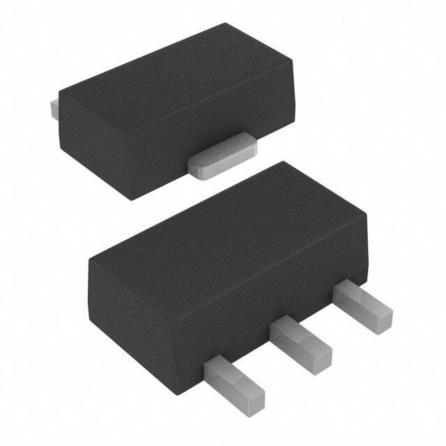
| 产品图片 |
|
| rohs | 符合RoHS无铅 / 符合限制有害物质指令(RoHS)规范要求 |
| 产品系列 | 电源管理 IC,低压差稳压器,Texas Instruments TPS726126DCQ- |
| 数据手册 | |
| 产品型号 | TPS726126DCQ |
| 产品目录页面 | |
| 产品种类 | 低压差稳压器 |
| 供应商器件封装 | SOT-223-6 |
| 其它名称 | 296-18257 |
| 包装 | 管件 |
| 单位重量 | 121 mg |
| 参考电压 | 1.22 V |
| 商标 | Texas Instruments |
| 安装类型 | 表面贴装 |
| 安装风格 | SMD/SMT |
| 封装 | Tube |
| 封装/外壳 | SOT-223-6 |
| 封装/箱体 | SOT-223-6 |
| 工作温度 | -40°C ~ 125°C |
| 工厂包装数量 | 78 |
| 最大工作温度 | + 125 C |
| 最大输入电压 | 6 V |
| 最小工作温度 | - 40 C |
| 最小输入电压 | + 1.8 V |
| 标准包装 | 78 |
| 电压-跌落(典型值) | - |
| 电压-输入 | 1.8 V ~ 6 V |
| 电压-输出 | 1.26V |
| 电压调节准确度 | 2 % |
| 电流-输出 | 1A |
| 电流-限制(最小值) | 1.1A |
| 稳压器拓扑 | 正,固定式 |
| 稳压器数 | 1 |
| 系列 | TPS726126 |
| 线路调整率 | 0.02 % / V |
| 负载调节 | 0.05 % / A |
| 输入偏压电流—最大 | 0.075 mA |
| 输出电压 | 1.26 V |
| 输出电流 | 1 A |
| 输出端数量 | 1 Output |
| 输出类型 | Fixed |


- 商务部:美国ITC正式对集成电路等产品启动337调查
- 曝三星4nm工艺存在良率问题 高通将骁龙8 Gen1或转产台积电
- 太阳诱电将投资9.5亿元在常州建新厂生产MLCC 预计2023年完工
- 英特尔发布欧洲新工厂建设计划 深化IDM 2.0 战略
- 台积电先进制程称霸业界 有大客户加持明年业绩稳了
- 达到5530亿美元!SIA预计今年全球半导体销售额将创下新高
- 英特尔拟将自动驾驶子公司Mobileye上市 估值或超500亿美元
- 三星加码芯片和SET,合并消费电子和移动部门,撤换高东真等 CEO
- 三星电子宣布重大人事变动 还合并消费电子和移动部门
- 海关总署:前11个月进口集成电路产品价值2.52万亿元 增长14.8%


PDF Datasheet 数据手册内容提取
TPS726126 TPS72615, TPS72616 TPS72618, TPS72625 www.ti.com SLVS403H–MAY2002–REVISEDJUNE2010 LOW INPUT VOLTAGE, 1-A LOW-DROPOUT LINEAR REGULATORS WITH SUPERVISOR CheckforSamples:TPS726126,TPS72615,TPS72616,TPS72618,TPS72625 FEATURES 1 DESCRIPTION • 1-ALow-DropoutRegulatorSupportsInput VoltagesDownto1.8-V The TPS726xx family of 1-A low-dropout (LDO) linear • Availablein1.26-V,1.5-V,1.6-V,1.8-V,2.5-V regulators has fixed voltage options available that are commonly used to power the latest DSPs, FPGAs, • StableWithAnyType/ValueOutputCapacitor and microcontrollers. The integrated supervisory • ±2%OutputVoltageToleranceOverLine, circuitry provides an active low RESET signal when Load,andTemperature(–40°Cto+125°C) the output falls out of regulation. The no • IntegratedSupervisor(SVS)With200-ms capacitor/any capacitor feature allows the customer RESETDelayTime to tailor output transient performance as needed. Therefore, compared to other regulators capable of • Low170-mVDropoutVoltageat1A providing the same output current, this family of (TPS72625) regulators can provide a stand alone power supply • Low210-mAGroundCurrentatFullLoad solution or a post regulator for a switch mode power • Lessthan1-mAStandbyCurrent supply. • IntegratedUVLOwithThermaland These regulators operate over a wide range of input OvercurrentProtection voltages (1.8 V to 6 V) and have very low dropout (170mVat1-A).Groundcurrentistypically210µAat • 5-LeadSOT223orDDPAKSurface-Mount full load and drops to less than 80µA at no load. Package Standbycurrentislessthan1µA. APPLICATIONS Unlike some regulators that have a minimum current requirement, the TPS726xx family is stable with no • PCICards output load current. The low noise capability of this • ModemBanksandTelecomBoards family, coupled with its high current operation and • DSP,FPGA,andMicroprocessorPower ease of power dissipation, make it ideal for telecom Supplies boards, modem banks, and other noise sensitive • Portable,Battery-PoweredApplications applications. • 1.26-VCoreVoltagefortheFollowingDSPs: The TPS726xx is available in either a SOT223 or – TMS320vC5501 DDPAK package. The TPS726126 is available in a – TMS320vC5502 SOT223packageonly. DCQ PACKAGE KTT PACKAGE SOT223-5 DDPAK (TOP VIEW) (TOP VIEW) ENABLE 1 IN 2 GND 3 OUT 4 1 2 3 4 5 RESET 5 ENDTT LINUE B GOS A E N R E Note: Tab is GND for both packages 1 Pleasebeawarethatanimportantnoticeconcerningavailability,standardwarranty,anduseincriticalapplicationsofTexas Instrumentssemiconductorproductsanddisclaimerstheretoappearsattheendofthisdatasheet. PRODUCTIONDATAinformationiscurrentasofpublicationdate. Copyright©2002–2010,TexasInstrumentsIncorporated Products conform to specifications per the terms of the Texas Instruments standard warranty. Production processing does not necessarilyincludetestingofallparameters.
TPS726126 TPS72615, TPS72616 TPS72618, TPS72625 SLVS403H–MAY2002–REVISEDJUNE2010 www.ti.com This integrated circuit can be damaged by ESD. Texas Instruments recommends that all integrated circuits be handled with appropriateprecautions.Failuretoobserveproperhandlingandinstallationprocedurescancausedamage. ESDdamagecanrangefromsubtleperformancedegradationtocompletedevicefailure.Precisionintegratedcircuitsmaybemore susceptibletodamagebecauseverysmallparametricchangescouldcausethedevicenottomeetitspublishedspecifications. ORDERINGINFORMATION(1) PRODUCT V OUT TPS726xxxyyyz XXXisnominaloutputvoltage(forexample,126=1.26V,15=1.5V). YYYispackagedesignator. Zispackagequantity. (1) Forthemostcurrentpackageandorderinginformation,seethePackageOptionAddendumattheendofthisdocument,orseetheTI websiteatwww.ti.com. ABSOLUTE MAXIMUM RATINGS overoperatingfree-airtemperaturerangeunlessotherwisenoted(1) UNIT Inputvoltage,V (2) –0.3to7 V I VoltagerangeatEN –0.3toV +0.3 V I VoltageonRESET V +0.3 V IN VoltageonOUT 6 V ESDrating,HBM 2 kV Continuoustotalpowerdissipation SeeDissipationRatingTable Operatingjunctiontemperaturerange,T –50to150 °C J Maximumjunctiontemperaturerange,T 150 °C J Storagetemperature,T –65to150 °C stg (1) Stressesbeyondthoselistedunderabsolutemaximumratingsmaycausepermanentdamagetothedevice.Thesearestressratings only,andfunctionaloperationofthedeviceattheseoranyotherconditionsbeyondthoseindicatedunderrecommendedoperating conditionsisnotimplied.Exposuretoabsolute-maximum-ratedconditionsforextendedperiodsmayaffectdevicereliability. (2) Allvoltagevaluesarewithrespecttonetworkgroundterminal. PACKAGE DISSIPATION RATINGS PACKAGE BOARD R R qJC qJA DDPAK HighK(1) 2°C/W 23°C/W SOT223 LowK(2) 15°C/W 53°C/W (1) TheJEDEChighK(2s2p)boarddesignusedtoderivethisdatawasa3-inchx3-inch(7,5-cmx7,5-cm),multilayerboardwith1ounce internalpowerandgroundplanesand2ouncecoppertracesontopandbottomoftheboard. (2) TheJEDEClowK(1s)boarddesignusedtoderivethisdatawasa3-inchx3-inch(7,5-cmx7,5-cm),two-layerboardwith2ounce coppertracesontopoftheboard. 2 SubmitDocumentationFeedback Copyright©2002–2010,TexasInstrumentsIncorporated ProductFolderLink(s):TPS726126TPS72615 TPS72616TPS72618 TPS72625
TPS726126 TPS72615, TPS72616 TPS72618, TPS72625 www.ti.com SLVS403H–MAY2002–REVISEDJUNE2010 ELECTRICAL CHARACTERISTICS overrecommendedoperatingfree-airtemperaturerangeV =V +1V,I =1mA,EN=IN,C =1µF,C =1µF(unless I O(typ) O O I otherwisenoted).Typicalvaluesareat+25°C. PARAMETER TESTCONDITIONS MIN TYP MAX UNIT V (1) Inputvoltage 1.8 6 V I I Continuousoutputcurrent 0 1 A O Bandgapvoltagereference 1.177 1.220 1.263 V TPS726126 0µA<I <1A 1.8V≤V ≤5.5V 1.222 1.26 1.298 O I TPS72615 0µA<I <1A 1.8V≤V ≤5.5V 1.47 1.5 1.53 O I V Outputvoltage TPS72616 0µA<I <1A 2.6V≤V ≤5.5V 1.568 1.6 1.632 V O O I TPS72618 0µA<I <1A 2.8V≤V ≤5.5V 1.764 1.8 1.836 O I TPS72625 0µA<I <1A 3.5V≤V ≤5.5V 2.45 2.5 2.55 O I I =0µA 75 120 O I Groundcurrent µA I =1A 210 300 O Standbycurrent EN<0.4V 0.2 1 µA V Outputnoisevoltage BW=200Hzto100kHz C =10µF 150 µV n O PSRR Ripplerejection f=1kHz,C =10µF 60 dB o Currentlimit(2) 1.1 1.6 2.3 A Outputvoltagelineregulation (ΔV /V )(3) VO+1V<VI≤5.5V –0.15 0.02 0.15 %/V O O Outputvoltageloadregulation 0µA<I <1A –0.25 0.05 0.25 %/A O V ENhighlevelinput 1.3 IH V V ENlowlevelinput –0.2 0.4 IL I ENinputcurrent EN=0VorV 0.01 100 nA I I UVLOthreshold V rising 1.45 1.57 1.70 V CC UVLOhysteresis V rising 50 mV CC UVLOdeglitch V rising 10 µs CC UVLOdelay V rising 100 µs CC TPS72625 I =1A 170 280 V Dropoutvoltage (4) O mV DO TPS72618 I =1A 210 320 O Minimuminputvoltageforvalid 1.3 V RESET(V ) RES Tripthresholdvoltage 90 93 96 %V O Hysteresisvoltage 10 mV RESET t delaytime 100 200 300 ms (RESET) Risingedgedeglitch 10 µs Outputlowvoltage(at700µA) –0.3 0.4 V Leakagecurrent 100 nA T Operatingjunctiontemperature –40 +125 °C J (1) MinimumV is1.800VorV +V ,whicheverisgreater. IN O DO (2) Testconditionincludes,outputvoltageV =V –15%andpulseduration=10ms. O O (3) V =(V +1)or1.8Vwhicheverisgreater. Imin O VO(cid:5)5.5V(cid:2)VImin(cid:6) Lineregulation(mV)(cid:3)(%(cid:4)V)(cid:1) 100 (cid:1)1000 (4) DropoutvoltageisdefinedasthedifferentialvoltagebetweenV andV whenV drops100mVbelowthevaluemeasuredwith O I O V =V +1V. I O Copyright©2002–2010,TexasInstrumentsIncorporated SubmitDocumentationFeedback 3 ProductFolderLink(s):TPS726126TPS72615 TPS72616TPS72618 TPS72625
TPS726126 TPS72615, TPS72616 TPS72618, TPS72625 SLVS403H–MAY2002–REVISEDJUNE2010 www.ti.com FUNCTIONALBLOCKDIAGRAM TPS726126/15/16 IN OUT EN Current Limit 1.220 / Thermal Vref Protection GND RESET Deglitch and Delay 0.93 × Vref TerminalFunctions TERMINAL DESCRIPTION NAME NO. GND 3 Ground ENABLE 1 Enableinput IN 2 Inputsupplyvoltage RESET 5 ThisterminalistheRESEToutput.Whenusedwithapull-upresistor,thisopen-drainoutputprovidestheactivelow RESETsignalwhentheregulatoroutputvoltagedropsmorethan5%belowitsnominaloutputvoltage.TheRESET delaytimeistypically200ms. OUT 4 Regulatedoutputvoltage RESETTIMINGDIAGRAM IN VRES VRES (see Note A) t OUT VIT+ VIT+ Threshold Voltage VIT− VIT− t RESET Output 200 ms 200 ms Î Delay Delay Î Î Î Output Output Î Î Undefined Undefined Î Î t Î Î NOTES:A. VRES is the minimÎum input voltage for a valid RESET. Î 4 SubmitDocumentationFeedback Copyright©2002–2010,TexasInstrumentsIncorporated ProductFolderLink(s):TPS726126TPS72615 TPS72616TPS72618 TPS72625
TPS726126 TPS72615, TPS72616 TPS72618, TPS72625 www.ti.com SLVS403H–MAY2002–REVISEDJUNE2010 TYPICAL CHARACTERISTICS TPS72618 TPS72618 TPS72618OUTPUTVOLTAGE OUTPUTVOLTAGE GROUNDCURRENT vs vs vs OUTPUTCURRENT JUNCTIONTEMPERATURE JUNCTIONTEMPERATURE 1.8015 1.805 250 1.801 VCTJIo === 221.5 8m° FVC V VCIo == 21. 8m FV A 200 VCTJIo === 221.5 8m° FVC IO = 1 A − Output Voltage − V 11..7890190.855 − Output Voltage − O11..789050 IO =IO 1 = A 0 mA mGround Current − 110500 IO = 0 mA O V 1.790 V 50 1.799 1.7985 1.785 0 0 0.2 0.4 0.6 0.8 1 −40−25−10 5 20 35 50 65 80 95 110125 −40−25−10 5 20 35 50 65 80 95110125 IO − Output Current − A TJ − Junction Temperature − °C TJ − Junction Temperature − °C Figure1. Figure2. Figure3. TPS72618 TPS72625 TPS72618 GROUNDCURRENT DCDROPOUTVOLTAGE DROPOUTVOLTAGE vs vs vs OUTPUTCURRENT OUTPUTCURRENT JUNCTIONTEMPERATURE 200 300 300 175 VO = 2.5 V (nom) VCOo == 11 .m7F V 250 V 250 V m A 150 m − mGround Current − 1102570505 − Dropout Voltage − O 112050000 TJ = 25°C TJ = 1T2J5 °=C −40°C − Dropout Voltage DO 112050000 IO = 1 A 25 VD 50 V 50 IO = 10 mA 0 0 0 0.01 0.1 1 10 100 1000 0 0.2 0.4 0.6 0.8 1 −40−25−10 5 20 35 50 65 80 95110125 IO − Output Current − mA IO − Output Current − A TJ − Junction Temperature − °C Figure4. Figure5. Figure6. Copyright©2002–2010,TexasInstrumentsIncorporated SubmitDocumentationFeedback 5 ProductFolderLink(s):TPS726126TPS72615 TPS72616TPS72618 TPS72625
TPS726126 TPS72615, TPS72616 TPS72618, TPS72625 SLVS403H–MAY2002–REVISEDJUNE2010 www.ti.com TYPICAL CHARACTERISTICS (continued) MINIMUMREQUIRED INPUTVOLTAGE TPS72618 TPS72618 vs LINETRANSIENT LOADTRANSIENT OUTPUTVOLTAGE RESPONSE RESPONSE 4.5 V V uired Input Voltage − V 3.534 TJ = 25°CTJ = 125°C − Input Voltage − VI 23..88 ICOo == 11 0A m F DV− Change inOAOutput Voltage − m−1100000 VCCOoi = == 1 12 0m.8 Fm VF − Minimum ReqVI 12..552 TJ = −40°C utput Voltage − mV −1100000 − Output Current − 0.501 1.5 2 VO −2 .O5utput3 Voltag3e.5 − V 4 4.5 − OVO 0 50 1001502t 0−0 T2im50e 3−0 m0s350400450500 IO 0 5 10 15t −2 0Tim2e5 − m3s0 35 40 45 50 Figure7. Figure8. Figure9. TPS72618 OUTPUTVOLTAGE, TPS72618 ENABLEVOLTAGE LOADTRANSIENT vs TPS72618 RESPONSE TIME(START-UP) POWERUP/POWERDOWN VD− Change inOI − Output Current − AOutput Voltage − mVO−11000.0510000 5 10 15 20 25 3VCC0IoI === 3 2151. 8mm F4FV0 45 50 V − Output Voltage − VEnable Voltage − VO10..5521100230 20 40 60 80 10012VICO0Io ===1 41210 .08A 1mV6F0180200 − Input Voltage − V− Output Voltage − VVOI 1350420 1RCC00Loi ===V2 10I11 0 .m8mF3 FW00VO4005006007008009001000 t − Time − m s t − Time − m s V t − Time − m s Figure10. Figure11. Figure12. 6 SubmitDocumentationFeedback Copyright©2002–2010,TexasInstrumentsIncorporated ProductFolderLink(s):TPS726126TPS72615 TPS72616TPS72618 TPS72625
TPS726126 TPS72615, TPS72616 TPS72618, TPS72625 www.ti.com SLVS403H–MAY2002–REVISEDJUNE2010 TYPICAL CHARACTERISTICS (continued) TPS72618 OUTPUTSPECTRALNOISE TPS72618 DENSITY RIPPLEREJECTION CURRENTLIMIT vs vs vs FREQUENCY FREQUENCY INPUTVOLTAGE 3.5 100 2000 mV/Hz 3 VCIo == 21.08 mVF B 9800 VVCIOO= ==2 .118.0 8V m,VF, 11890000 TJ = 125°C y − 2.5 − d 70 A 1700 ctral Noise Densit 1.512 IO = 1 A Ripple Rejection 53640000 10 m F / 1mA Current Limit − 1111345600000000 TJ = −40°CTJ = 25°C put Spe 0.5 IO = 1 mA 2100 10 m F / 1A 11210000 Out 0 0 1000 10 100 1 k 10 k 100 k 10 100 1 k 10 k 100 k 1 M 1.5 2 2.5 3 3.5 4 4.5 5 5.5 f − Frequency − Hz f − Frequency − Hz VI − Input voltage − V Figure13. Figure14. Figure15. TPS72615 GROUNDCURRENT DROPOUTVOLTAGE vs vs INPUTVOLTAGE INPUTVOLTAGE 600 300 500 V 250 TJ = 125°C m − TJ = 25°C A e 400 g 200 mCurrent − 300 I = 1 A pout Volta 150 ound 200 − Dro 100 Gr I = 0 A DO TJ = −40°C 100 V 50 0 0 0 1 2 3 4 5 6 1.5 2 2.5 3 3.5 4 4.5 5 5.5 VI − Input Voltage − V VI − Input Voltage − V Figure16. Figure17. Copyright©2002–2010,TexasInstrumentsIncorporated SubmitDocumentationFeedback 7 ProductFolderLink(s):TPS726126TPS72615 TPS72616TPS72618 TPS72625
TPS726126 TPS72615, TPS72616 TPS72618, TPS72625 SLVS403H–MAY2002–REVISEDJUNE2010 www.ti.com APPLICATION INFORMATION The TPS726xx family of low-dropout (LDO) regulators have numerous features that make it apply to a wide range of applications. The family operates with very low input voltage (≥1.8 V) and low dropout voltage (typically 200 mV at full load), making it an efficient stand-alone power supply or post regulator for battery or switch mode power supplies. Both the active low RESET and 1-A output current, make the TPS726xx family ideal for powering processor and FPGA supplies. The TPS726xx family also has low output noise (typically 150 µV RMS with10-µFoutputcapacitor),makingitidealforuseintelecomequipment. External Capacitor Requirements A 1-µF or larger ceramic input bypass capacitor, connected between IN and GND and located close to the TPS726xx, is required for stability. To improve transient response, noise rejection, and ripple rejection, an additional 10-µF or larger, low ESR capacitor is recommended. A higher-value, low ESR input capacitor may be necessary if large, fast-rise-time load transients are anticipated and the device is located several inches from the powersource,especiallyiftheminimuminputvoltageof1.8Visused. Althoughanoutputcapacitorisnotrequiredforstability,transientresponseandoutputnoiseareimprovedwitha 10-µFoutputcapacitor. TPS726xx V IN OUT V I O 1mF 10 kW C O EN RESET GND Figure18. TPS726xxFixedOutputTypicalApplicationDiagram Regulator Protection The TPS726xx pass element has a built-in back diode that safely conducts reverse current when the input voltage drops below the output voltage (e.g., during power down). Current is conducted from the output to the input and is not internally limited. If extended reverse voltage is anticipated, external limiting might be appropriate. The TPS726xx also features internal current limiting and thermal protection. During normal operation, the TPS726xx limits output current to approximately 1.6 A. When current limiting engages, the output voltage scales back linearly until the overcurrent condition ends. While current limiting is designed to prevent gross device failure,careshouldbetakennottoexceedthepowerdissipationratingsofthepackage.Ifthetemperatureofthe device exceeds 165°C, thermal-protection circuitry shuts it down. Once the device has cooled down to below 145°C,regulatoroperationresumes. THERMAL INFORMATION The amount of heat that an LDO linear regulator generates is directly proportional to the amount of power it dissipates during operation. All integrated circuits have a maximum allowable junction temperature (T max) J above which normal operation is not assured. A system designer must design the operating environment so that the operating junction temperature (T ) does not exceed the maximum junction temperature (T max). The two J J main environmental variables that a designer can use to improve thermal performance are air flow and external heatsinks. The purpose of this information is to aid the designer in determining the proper operating environment foralinearregulatorthatisoperatingataspecificpowerlevel. 8 SubmitDocumentationFeedback Copyright©2002–2010,TexasInstrumentsIncorporated ProductFolderLink(s):TPS726126TPS72615 TPS72616TPS72618 TPS72625
TPS726126 TPS72615, TPS72616 TPS72618, TPS72625 www.ti.com SLVS403H–MAY2002–REVISEDJUNE2010 Ingeneral,themaximumexpectedpower(P )consumedbyalinearregulatoriscomputedas: D(max) (cid:5) (cid:6) PDmax(cid:4) VI(avg)(cid:3)VO(avg) (cid:1)IO(avg) (cid:2) VI(avg)xI(Q) (1) Where: • V istheaverageinputvoltage. I(avg) • V istheaverageoutputvoltage. O(avg) • istheaverageoutputcurrent. O(avg) • I isthequiescentcurrent. (Q) For most TI LDO regulators, the quiescent current is insignificant compared to the average output current; therefore, the term V x I can be neglected. The operating junction temperature is computed by adding the I(avg) (Q) ambient temperature (T ) and the increase in temperature due to the regulator's power dissipation. The A temperature rise is computed by multiplying the maximum expected power dissipation by the sum of the thermal resistances between the junction and the case ® ), the case to heatsink ® ), and the heatsink to ambient qJC qCS ® ). Thermal resistances are measures of how effectively an object dissipates heat. Typically, the larger the qSA device,themoresurfaceareaavailableforpowerdissipationandthelowertheobject'sthermalresistance. Figure 19 illustrates these thermal resistances for (a) a SOT223 package mounted in a JEDEC low-K board, and (b)aDDPAKpackagemountedonaJEDEChigh-Kboard. A TJ Rq JC A CIRCUIT BOARD COPPER AREA B C B TC B Rq CS A C Rq SA C DDPAK Package SOT223 Package TA (b) (a) Figure19. ThermalResistances Equation2summarizesthecomputation: TJ (cid:2) TA(cid:1)PDmaxx(cid:3)Rq JC (cid:1) Rq CS (cid:1) Rq SA(cid:4) (2) The R is specific to each regulator as determined by its package, lead frame, and die size provided in the qJC regulator's data sheet. The R is a function of the type and size of heatsink. For example, black body radiator qSA type heatsinks can have R values ranging from 5°C/W for very large heatsinks to 50°C/W for very small qCS heatsinks. The R is a function of how the package is attached to the heatsink. For example, if a thermal qCS compoundisusedtoattachaheatsinktoaSOT223package,R of1°C/Wisreasonable. qCS Even if no external black body radiator type heatsink is attached to the package, the board on which the regulator is mounted provides some heatsinking through the pin solder connections. Some packages, like the DDPAK and SOT223 packages, use a copper plane underneath the package or the circuit board's ground plane for additional heatsinking to improve their thermal performance. Computer-aided thermal modeling can be used to compute very accurate approximations of an integrated circuit's thermal performance in different operating environments (e.g., different types of circuit boards, different types and sizes of heatsinks, and different air flows, etc.). Using these models, the three thermal resistances can be combined into one thermal resistance between junction and ambient ® ). This R is valid only for the specific operating environment used in the computer qJA qJA model. Copyright©2002–2010,TexasInstrumentsIncorporated SubmitDocumentationFeedback 9 ProductFolderLink(s):TPS726126TPS72615 TPS72616TPS72618 TPS72625
TPS726126 TPS72615, TPS72616 TPS72618, TPS72625 SLVS403H–MAY2002–REVISEDJUNE2010 www.ti.com Equation2simplifiesintoEquation3: TJ (cid:2) TA(cid:1)PDmaxx Rq JA (3) RearrangingEquation3givesEquation4: T –T J A Rq JA (cid:1) P max D (4) Using Equation 3 and the computer model generated curves shown in Figure 20 and Figure 23, a designer can quickly compute the required heatsink thermal resistance/board area for a given ambient temperature, power dissipation,andoperatingenvironment. DDPAK Power Dissipation The DDPAK package provides an effective means of managing power dissipation in surface mount applications. The DDPAK package dimensions are provided in the Mechanical Data section at the end of the data sheet. The addition of a copper plane directly underneath the DDPAK package enhances the thermal performance of the package. To illustrate, the TPS72625 in a DDPAK package was chosen. For this example, the average input voltage is 5 V, the output voltage is 2.5 V, the average output current is 1 A, the ambient temperature 55°C, the air flow is 150 LFM, and the operating environment is the same as documented below. Neglecting the quiescent current, themaximumaveragepoweris: PDmax (cid:2) (5 (cid:1) 2.5)Vx1A (cid:2) 2.5W (5) SubstitutingT maxforT intoEquation4givesEquation6: J J Rq JAmax (cid:2) (125 (cid:1) 55)°C(cid:3)2.5W (cid:2) 28°C(cid:3)W (6) From Figure 20, DDPAK Thermal Resistance vs Copper Heatsink Area, the ground plane needs to be 1 cm2 for the part to dissipate 2.5 W. The operating environment used in the computer model to construct Figure 20 consisted of a standard JEDEC High-K board (2S2P) with a 1 oz. internal copper plane and ground plane. The package is soldered to a 2 oz. copper pad. The pad is tied through thermal vias to the 1 oz. ground plane. Figure21showsthesideviewoftheoperatingenvironmentusedinthecomputermodel. 40 No Air Flow W C/ 35 ° − e 150 LFM c n a st 30 si e R mal 250 LFM er 25 h T − A J Rq 20 15 0.1 1 10 100 Copper Heatsink Area − cm2 Figure20. DDPAKThermalResistancevsCopperHeatsinkArea 10 SubmitDocumentationFeedback Copyright©2002–2010,TexasInstrumentsIncorporated ProductFolderLink(s):TPS726126TPS72615 TPS72616TPS72618 TPS72625
TPS726126 TPS72615, TPS72616 TPS72618, TPS72625 www.ti.com SLVS403H–MAY2002–REVISEDJUNE2010 2 oz. Copper Solder Pad with 25 Thermal Vias 1 oz. Copper Power Plane 1 oz. Copper Ground Plane Thermal Vias, 0,3 mm Diameter, 1,5 mm Pitch Figure21. DDPAKThermalResistance From the data in Figure 22 and rearranging Equation 4, the maximum power dissipation for a different ground planeareaandaspecificambienttemperaturecanbecomputed. 5 C TA = 55°C °5 W 12 − − ation 4 250 LFM ature sip per s m Di e er 150 LFM n T w 3 o Po cti m un u J m m xi No Air Flow u a m − M 2 axi D M P − M TJ 1 0.1 1 10 100 Copper Heatsink Area − cm2 Figure22. MaximumPowerDissipationvsCopperHeatsinkArea SOT223 Power Dissipation The SOT223 package provides an effective means of managing power dissipation in surface mount applications. The SOT223 package dimensions are provided in the Mechanical Data section at the end of the data sheet. The addition of a copper plane directly underneath the SOT223 package enhances the thermal performance of the package. To illustrate, the TPS72625 in a SOT223 package was chosen. For this example, the average input voltage is 3.3 V, the output voltage is 2.5 V, the average output current is 1 A, the ambient temperature 55°C, no air flow is present, and the operating environment is the same as documented below. Neglecting the quiescent current, the maximumaveragepoweris: PDmax (cid:2) (3.3 (cid:1) 2.5)Vx1A (cid:2) 800mW (7) SubstitutingT maxforT intoEquation4givesEquation8: J J Copyright©2002–2010,TexasInstrumentsIncorporated SubmitDocumentationFeedback 11 ProductFolderLink(s):TPS726126TPS72615 TPS72616TPS72618 TPS72625
TPS726126 TPS72615, TPS72616 TPS72618, TPS72625 SLVS403H–MAY2002–REVISEDJUNE2010 www.ti.com Rq JAmax (cid:2) (125 (cid:1) 55)°C(cid:3)800mW (cid:2) 87.5°C(cid:3)W (8) From Figure 23, R vs PCB Copper Area, the ground plane needs to be 0.55 in2 for the part to dissipate 800 qJA mW. The operating environment used to construct Figure 23 consisted of a board with 1 oz. copper planes. The package is soldered to a 1 oz. copper pad on the top of the board. The pad is tied through thermal vias to the 1 oz.groundplane. 180 No Air Flow 160 W C/ 140 ° − e c 120 n a st si 100 e R mal 80 er h T 60 − A J 40 Rq 20 0 0.1 1 10 PCB Copper Area − in2 Figure23. SOT223ThermalResistancevsPCBAREA From the data in Figure 23 and rearranging Equation 4, the maximum power dissipation for a different ground planeareaandaspecificambienttemperaturecanbecomputed(asshowninFigure24). 6 TA = 25°C W − 5 n o ati p 4 si s Di 4 in2 PCB Area r e w 3 o P m mu 2 0.5 in2 PCB Area xi a M − PD 1 0 0 25 50 75 100 125 150 TA − Ambient Temperature − °C Figure24. SOT223PowerDissipation 12 SubmitDocumentationFeedback Copyright©2002–2010,TexasInstrumentsIncorporated ProductFolderLink(s):TPS726126TPS72615 TPS72616TPS72618 TPS72625
TPS726126 TPS72615, TPS72616 TPS72618, TPS72625 www.ti.com SLVS403H–MAY2002–REVISEDJUNE2010 REVISION HISTORY NOTE:Pagenumbersforpreviousrevisionsmaydifferfrompagenumbersinthecurrentversion. ChangesfromRevisionG(May2006)toRevisionH Page • DeletedFigure14,OutputImpedancevsFrequency ........................................................................................................... 7 • AddedFigure18 ................................................................................................................................................................... 8 Copyright©2002–2010,TexasInstrumentsIncorporated SubmitDocumentationFeedback 13 ProductFolderLink(s):TPS726126TPS72615 TPS72616TPS72618 TPS72625
PACKAGE OPTION ADDENDUM www.ti.com 6-Feb-2020 PACKAGING INFORMATION Orderable Device Status Package Type Package Pins Package Eco Plan Lead/Ball Finish MSL Peak Temp Op Temp (°C) Device Marking Samples (1) Drawing Qty (2) (6) (3) (4/5) TPS726126DCQ ACTIVE SOT-223 DCQ 6 78 Green (RoHS NIPDAU Level-2-260C-1 YEAR -40 to 125 726126 & no Sb/Br) TPS726126DCQR ACTIVE SOT-223 DCQ 6 2500 Green (RoHS NIPDAU Level-2-260C-1 YEAR -40 to 125 726126 & no Sb/Br) TPS726126DCQRG4 ACTIVE SOT-223 DCQ 6 2500 Green (RoHS NIPDAU Level-2-260C-1 YEAR -40 to 125 726126 & no Sb/Br) TPS72615DCQ ACTIVE SOT-223 DCQ 6 78 Green (RoHS NIPDAU Level-2-260C-1 YEAR -40 to 125 PS72615 & no Sb/Br) TPS72615DCQR ACTIVE SOT-223 DCQ 6 2500 Green (RoHS NIPDAU Level-2-260C-1 YEAR -40 to 125 PS72615 & no Sb/Br) TPS72615KTTR ACTIVE DDPAK/ KTT 5 500 Green (RoHS Call TI | SN Level-2-260C-1 YEAR -40 to 125 TPS TO-263 & no Sb/Br) 72615 TPS72616DCQ ACTIVE SOT-223 DCQ 6 78 Green (RoHS NIPDAU Level-2-260C-1 YEAR -40 to 125 PS72616 & no Sb/Br) TPS72616DCQR ACTIVE SOT-223 DCQ 6 2500 Green (RoHS NIPDAU Level-2-260C-1 YEAR -40 to 125 PS72616 & no Sb/Br) TPS72616KTTR ACTIVE DDPAK/ KTT 5 500 Green (RoHS Call TI | SN Level-2-260C-1 YEAR TPS TO-263 & no Sb/Br) 72616 TPS72616KTTRG3 ACTIVE DDPAK/ KTT 5 500 Green (RoHS SN Level-2-260C-1 YEAR TPS TO-263 & no Sb/Br) 72616 TPS72618DCQ ACTIVE SOT-223 DCQ 6 78 Green (RoHS NIPDAU Level-2-260C-1 YEAR PS72618 & no Sb/Br) TPS72618DCQR ACTIVE SOT-223 DCQ 6 2500 Green (RoHS NIPDAU Level-2-260C-1 YEAR PS72618 & no Sb/Br) TPS72618KTTR ACTIVE DDPAK/ KTT 5 500 Green (RoHS Call TI | SN Level-2-260C-1 YEAR TPS TO-263 & no Sb/Br) 72618 TPS72625DCQ ACTIVE SOT-223 DCQ 6 78 Green (RoHS NIPDAU Level-2-260C-1 YEAR PS72625 & no Sb/Br) TPS72625DCQR ACTIVE SOT-223 DCQ 6 2500 Green (RoHS NIPDAU Level-2-260C-1 YEAR PS72625 & no Sb/Br) TPS72625KTTT ACTIVE DDPAK/ KTT 5 50 Green (RoHS Call TI | SN Level-2-260C-1 YEAR -40 to 125 TPS TO-263 & no Sb/Br) 72625 (1) The marketing status values are defined as follows: ACTIVE: Product device recommended for new designs. Addendum-Page 1
PACKAGE OPTION ADDENDUM www.ti.com 6-Feb-2020 LIFEBUY: TI has announced that the device will be discontinued, and a lifetime-buy period is in effect. NRND: Not recommended for new designs. Device is in production to support existing customers, but TI does not recommend using this part in a new design. PREVIEW: Device has been announced but is not in production. Samples may or may not be available. OBSOLETE: TI has discontinued the production of the device. (2) RoHS: TI defines "RoHS" to mean semiconductor products that are compliant with the current EU RoHS requirements for all 10 RoHS substances, including the requirement that RoHS substance do not exceed 0.1% by weight in homogeneous materials. Where designed to be soldered at high temperatures, "RoHS" products are suitable for use in specified lead-free processes. TI may reference these types of products as "Pb-Free". RoHS Exempt: TI defines "RoHS Exempt" to mean products that contain lead but are compliant with EU RoHS pursuant to a specific EU RoHS exemption. Green: TI defines "Green" to mean the content of Chlorine (Cl) and Bromine (Br) based flame retardants meet JS709B low halogen requirements of <=1000ppm threshold. Antimony trioxide based flame retardants must also meet the <=1000ppm threshold requirement. (3) MSL, Peak Temp. - The Moisture Sensitivity Level rating according to the JEDEC industry standard classifications, and peak solder temperature. (4) There may be additional marking, which relates to the logo, the lot trace code information, or the environmental category on the device. (5) Multiple Device Markings will be inside parentheses. Only one Device Marking contained in parentheses and separated by a "~" will appear on a device. If a line is indented then it is a continuation of the previous line and the two combined represent the entire Device Marking for that device. (6) Lead/Ball Finish - Orderable Devices may have multiple material finish options. Finish options are separated by a vertical ruled line. Lead/Ball Finish values may wrap to two lines if the finish value exceeds the maximum column width. Important Information and Disclaimer:The information provided on this page represents TI's knowledge and belief as of the date that it is provided. TI bases its knowledge and belief on information provided by third parties, and makes no representation or warranty as to the accuracy of such information. Efforts are underway to better integrate information from third parties. TI has taken and continues to take reasonable steps to provide representative and accurate information but may not have conducted destructive testing or chemical analysis on incoming materials and chemicals. TI and TI suppliers consider certain information to be proprietary, and thus CAS numbers and other limited information may not be available for release. In no event shall TI's liability arising out of such information exceed the total purchase price of the TI part(s) at issue in this document sold by TI to Customer on an annual basis. Addendum-Page 2
PACKAGE MATERIALS INFORMATION www.ti.com 12-Jun-2019 TAPE AND REEL INFORMATION *Alldimensionsarenominal Device Package Package Pins SPQ Reel Reel A0 B0 K0 P1 W Pin1 Type Drawing Diameter Width (mm) (mm) (mm) (mm) (mm) Quadrant (mm) W1(mm) TPS726126DCQR SOT-223 DCQ 6 2500 330.0 12.4 7.1 7.45 1.88 8.0 12.0 Q3 TPS72615DCQR SOT-223 DCQ 6 2500 330.0 12.4 7.1 7.45 1.88 8.0 12.0 Q3 TPS72615KTTR DDPAK/ KTT 5 500 330.0 24.4 10.6 15.6 4.9 16.0 24.0 Q2 TO-263 TPS72616DCQR SOT-223 DCQ 6 2500 330.0 12.4 7.1 7.45 1.88 8.0 12.0 Q3 TPS72616KTTR DDPAK/ KTT 5 500 330.0 24.4 10.6 15.6 4.9 16.0 24.0 Q2 TO-263 TPS72618DCQR SOT-223 DCQ 6 2500 330.0 12.4 7.1 7.45 1.88 8.0 12.0 Q3 TPS72618KTTR DDPAK/ KTT 5 500 330.0 24.4 10.6 15.6 4.9 16.0 24.0 Q2 TO-263 TPS72625DCQR SOT-223 DCQ 6 2500 330.0 12.4 7.1 7.45 1.88 8.0 12.0 Q3 TPS72625KTTT DDPAK/ KTT 5 50 330.0 24.4 10.6 15.6 4.9 16.0 24.0 Q2 TO-263 PackMaterials-Page1
PACKAGE MATERIALS INFORMATION www.ti.com 12-Jun-2019 *Alldimensionsarenominal Device PackageType PackageDrawing Pins SPQ Length(mm) Width(mm) Height(mm) TPS726126DCQR SOT-223 DCQ 6 2500 346.0 346.0 41.0 TPS72615DCQR SOT-223 DCQ 6 2500 346.0 346.0 29.0 TPS72615KTTR DDPAK/TO-263 KTT 5 500 367.0 367.0 45.0 TPS72616DCQR SOT-223 DCQ 6 2500 346.0 346.0 41.0 TPS72616KTTR DDPAK/TO-263 KTT 5 500 367.0 367.0 45.0 TPS72618DCQR SOT-223 DCQ 6 2500 346.0 346.0 41.0 TPS72618KTTR DDPAK/TO-263 KTT 5 500 367.0 367.0 45.0 TPS72625DCQR SOT-223 DCQ 6 2500 346.0 346.0 41.0 TPS72625KTTT DDPAK/TO-263 KTT 5 50 367.0 367.0 45.0 PackMaterials-Page2
None
None
None
None
IMPORTANTNOTICEANDDISCLAIMER TI PROVIDES TECHNICAL AND RELIABILITY DATA (INCLUDING DATASHEETS), DESIGN RESOURCES (INCLUDING REFERENCE DESIGNS), APPLICATION OR OTHER DESIGN ADVICE, WEB TOOLS, SAFETY INFORMATION, AND OTHER RESOURCES “AS IS” AND WITH ALL FAULTS, AND DISCLAIMS ALL WARRANTIES, EXPRESS AND IMPLIED, INCLUDING WITHOUT LIMITATION ANY IMPLIED WARRANTIES OF MERCHANTABILITY, FITNESS FOR A PARTICULAR PURPOSE OR NON-INFRINGEMENT OF THIRD PARTY INTELLECTUAL PROPERTY RIGHTS. These resources are intended for skilled developers designing with TI products. You are solely responsible for (1) selecting the appropriate TI products for your application, (2) designing, validating and testing your application, and (3) ensuring your application meets applicable standards, and any other safety, security, or other requirements. These resources are subject to change without notice. TI grants you permission to use these resources only for development of an application that uses the TI products described in the resource. Other reproduction and display of these resources is prohibited. No license is granted to any other TI intellectual property right or to any third party intellectual property right. TI disclaims responsibility for, and you will fully indemnify TI and its representatives against, any claims, damages, costs, losses, and liabilities arising out of your use of these resources. TI’s products are provided subject to TI’s Terms of Sale (www.ti.com/legal/termsofsale.html) or other applicable terms available either on ti.com or provided in conjunction with such TI products. TI’s provision of these resources does not expand or otherwise alter TI’s applicable warranties or warranty disclaimers for TI products. Mailing Address: Texas Instruments, Post Office Box 655303, Dallas, Texas 75265 Copyright © 2020, Texas Instruments Incorporated