ICGOO在线商城 > 集成电路(IC) > PMIC - 电源管理 - 专用 > TPS65140IPWPRQ1
 Datasheet下载
- 型号: TPS65140IPWPRQ1
- 制造商: Texas Instruments
- 库位|库存: xxxx|xxxx
- 要求:
| 数量阶梯 | 香港交货 | 国内含税 |
| +xxxx | $xxxx | ¥xxxx |
查看当月历史价格
查看今年历史价格
TPS65140IPWPRQ1产品简介:
ICGOO电子元器件商城为您提供TPS65140IPWPRQ1由Texas Instruments设计生产,在icgoo商城现货销售,并且可以通过原厂、代理商等渠道进行代购。 TPS65140IPWPRQ1价格参考。Texas InstrumentsTPS65140IPWPRQ1封装/规格:PMIC - 电源管理 - 专用, LCD Monitor, Notebook Display PMIC 24-HTSSOP。您可以下载TPS65140IPWPRQ1参考资料、Datasheet数据手册功能说明书,资料中有TPS65140IPWPRQ1 详细功能的应用电路图电压和使用方法及教程。
| 参数 | 数值 |
| 产品目录 | 集成电路 (IC) |
| 描述 | IC LCD SUPP W/LINEAR REG 24TSSOP |
| 产品分类 | |
| 品牌 | Texas Instruments |
| 数据手册 | |
| 产品图片 |
|
| 产品型号 | TPS65140IPWPRQ1 |
| PCN组件/产地 | |
| rohs | 含铅 / 不符合限制有害物质指令(RoHS)规范要求 |
| 产品系列 | - |
| 产品目录页面 | |
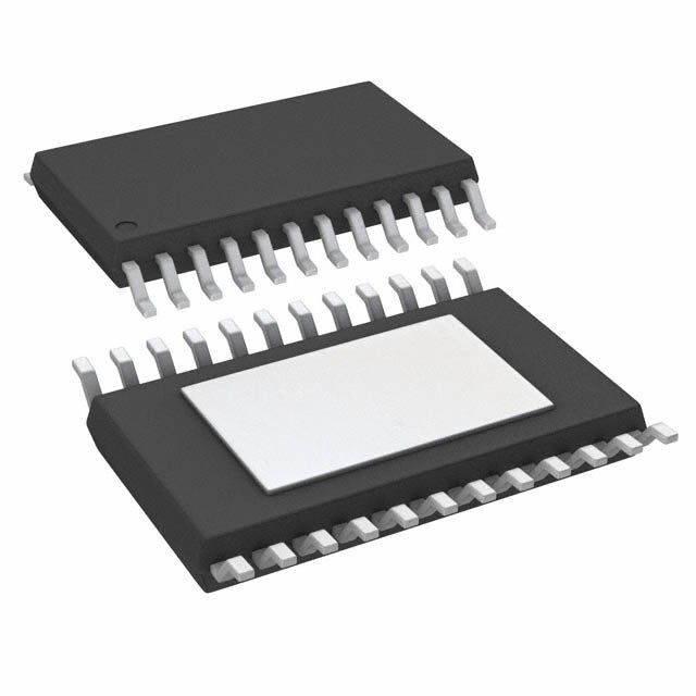
| 供应商器件封装 | 24-HTSSOP |
| 其它名称 | 296-19612-6 |
| 包装 | Digi-Reel® |
| 安装类型 | 表面贴装 |
| 封装/外壳 | 24-TSSOP(0.173",4.40mm 宽)裸焊盘 |
| 工作温度 | -40°C ~ 85°C |
| 应用 | LCD 监视器,笔记本电脑显示器 |
| 标准包装 | 1 |
| 电压-电源 | 2.7 V ~ 5.8 V |
| 电流-电源 | 700µA |
| 配用 | /product-detail/zh/TPS65140EVM-031/296-18997-ND/863819 |


PDF Datasheet 数据手册内容提取
Product Order Technical Tools & Support & Folder Now Documents Software Community TPS65140-Q1 TPS65145-Q1 SGLS277B–NOVEMBER2004–REVISEDSEPTEMBER2017 TPS65140/5-Q1 Triple Output LCD Supply with Linear Regulator and Power Good 1 Features 2 Applications • QualifiedforAutomotiveApplications • InfotainmentSystems 1 • AEC-Q100QualifiedWiththeFollowingResults: • AutomotiveDisplays – DeviceTemperatureGrade1 • InstrumentClusters – DeviceHBMESDClassificationLevelH2 • CenterConsoles – DeviceCDMESDClassificationLevelC5 • RearSeatEntertainment • InputVoltageRange:2.7Vto5.8V 3 Description • V 1BoostConverter O The TPS65140-Q1 and TPS65145-Q1 devices offer a – Upto15VOutputVoltage compact and small power supply solution that – VirtualSynchronousConverterTopology provides all three voltages required by thin-film – < 1%OutputVoltageAccuracy transistor (TFT) LCD displays. The auxiliary linear regulator controller can be used to generate a 3.3-V – 1.6-MHzFixedSwitchingFrequency logic power rail for systems powered by a 5-V supply – 2.3-ASwitchCurrentLimit railonly. • V 2NegativeRegulatedChargePump O The main output, V 1 is a 1.6-MHz fixed-frequency O – Downto-12V/20mA PWM boost converter providing the source-drive • V 3PositiveRegulatedChargePump voltage for the LCD display. The TPS65140-Q1 O device has a typical switch current limit of 2.3 A and – Upto30V/20mA the TPS65145-Q1 has a typical switch current limit of • ThreeIndependentlyAdjustableOutputs 1.37A. • Auxiliary3.3-VLinearRegulatorController A fully integrated adjustable charge pump doubler • InternalSoftStart and provides the positive LCD gate-drive voltage. An • PowerGood externally adjustable negative charge pump provides thenegativeLCDgate-drivevoltage. • ProtectionFeatures – Short-CircuitDetectionofallOutputs DeviceInformation(1) – OvervoltageProtectionofallOutputs PARTNUMBER PACKAGE BODYSIZE(NOM) – ThermalShutdown TPS65140-Q1 TSSOP(24)with 4.40mm×7.80mm • AvailableinTSSOP-24 PowerPAD™Package TPS65145-Q1 PowerPAD (1) For all available packages, see the orderable addendum at theendofthedatasheet. spacer DeviceBlockDiagram TypicalApplicationCircuit TPS65140 / 45 VIN Boost VO1 2.7 V tVoI 5.8 V 4.2L1μH D1 Up to 15V OV1/350 mA 2.7 V to 5.8 V Converter Up to 15 V / 400 mA C3 22μF TPS65140-Q1 C5 R1 C4 Positive Charge VO3 C13 10 nF VCIONMP SSWW 22μF Pump Up to 30 V / 20 mA GND FB1 ChNaerggea tPivuemp VUOp2 to–12 V / 20 mA Up to 1V2O V2/20 mA D2 C1C21 00..2222μμFF EECCDNN11R+−RV C2−/MOOSFUCUDBT2PE+33 C1 0.22μF R2 Up to 3V0O V3/20 mA Power Good Power Good FB2 PG Linear Regulator VO4 0.22CμF6 R3 D3 RFBE4F PPGGNNDD R5 C0.722μF Controller 3.3 V BASE GND R4 R6 100C n1F1 VI BCQP168 V3.O34 V VI R7 1CμF9 C4.97μF 33 kΩ SysGteomo dPower Copyright © 2016,Texas Instruments Incorporated 1 An IMPORTANT NOTICE at the end of this data sheet addresses availability, warranty, changes, use in safety-critical applications, intellectualpropertymattersandotherimportantdisclaimers.PRODUCTIONDATA.
TPS65140-Q1 TPS65145-Q1 SGLS277B–NOVEMBER2004–REVISEDSEPTEMBER2017 www.ti.com Table of Contents 1 Features.................................................................. 1 11 ApplicationandImplementation........................ 13 2 Applications........................................................... 1 11.1 ApplicationInformation..........................................13 3 Description............................................................. 1 11.2 TypicalApplication ...............................................13 4 RevisionHistory..................................................... 2 11.3 SystemExamples ................................................21 5 Description(Continued)........................................ 3 12 PowerSupplyRecommendations..................... 22 6 DeviceComparison............................................... 3 13 Layout................................................................... 22 13.1 LayoutGuidelines.................................................22 7 PinConfigurationandFunctions......................... 3 13.2 ThermalInformation..............................................22 8 Specifications......................................................... 4 13.3 LayoutExample....................................................23 8.1 AbsoluteMaximumRatings......................................4 14 DeviceandDocumentationSupport................. 24 8.2 ESDRatings..............................................................4 14.1 DeviceSupport ....................................................24 8.3 RecommendedOperatingConditions.......................4 14.2 RelatedLinks........................................................24 8.4 ThermalInformation..................................................5 14.3 DocumentationSupport .......................................24 8.5 ElectricalCharacteristics...........................................5 14.4 ReceivingNotificationofDocumentationUpdates24 9 TypicalCharacteristics.......................................... 8 14.5 CommunityResources..........................................24 10 DetailedDescription............................................. 9 14.6 Trademarks...........................................................24 10.1 Overview.................................................................9 14.7 ElectrostaticDischargeCaution............................24 10.2 FunctionalBlockDiagram.....................................10 14.8 Glossary................................................................25 10.3 FeatureDescription...............................................11 15 Mechanical,Packaging,andOrderable 10.4 DeviceFunctionalModes......................................11 Information........................................................... 25 4 Revision History NOTE:Pagenumbersforpreviousrevisionsmaydifferfrompagenumbersinthecurrentversion. ChangesfromRevisionA(April2008)toRevisionB Page • AddedDeviceInformationtable,PinConfigurationandFunctionssection,Specificationssection,Feature Descriptionsection,DeviceFunctionalModessection,ApplicationandImplementationsection,PowerSupply Recommendationssection,Layoutsection,DeviceandDocumentationSupportsection,andMechanical, Packaging,andOrderableInformationsection...................................................................................................................... 1 • DeletedDissipationRatingstableandaddedThermalInformationandESDRatingstables................................................ 4 • ChangedfromT toT intheConditionsstatementofElectricalCharacteristicsandchangedtemperaturefrom85°C A J to125°C.................................................................................................................................................................................. 5 • ChangedtheMAINBOOSTCONVERTERV specfrom1.205MINto1.198,andMAXfrom1.219to1.230 ................ 5 REF • ChangedtheMAINBOOSTCONVERTERV specfrom1.136MINto1.126,andMAXfrom1.154to1.161................... 5 FB • ChangedtheMAINBOOSTCONVERTERr specforV 1=10V,Isw=500mAcondition,from290to325 DS(ON) O MAX;and,fortheV 1=5V,Isw=500mAcondition,changedfrom420to455MAX........................................................ 5 O • ChangedtheMAINBOOSTCONVERTERf specfor0°C≤T ≤125°Cconditionfrom1.295MINto1.195MIN; SW A and,forthe–40°C≤T ≤125°Ccondition,changedtheMINfrom1.191to1.091............................................................... 6 A • ChangedtheNEGATIVECHARGEPUMPV 2V specfrom1.205MINto1.198,andMAXfrom1.219to1.226 ...........6 O ref • ChangedfromT toT intheConditionsstatementofElectricalCharacteristicsandchangedtemperaturefrom85°C A J to125°C.................................................................................................................................................................................. 6 • ChangedthePOSITIVECHARGEPUMPV 3V specfrom1.205MINto1.198,andMAXfrom1.219to1.226.............6 O ref • ChangedthePOSITIVECHARGEPUMPV specfrom1.187MINto1.180,andMAXfrom1.238to1.245.................... 6 FB • ChangedthePOSITIVECHARGEPUMPV 3V specfrom720mVMAXto800mV ....................................................... 6 O d • ChangedfromT toT intheConditionsstatementofElectricalCharacteristicsandchangedtemperaturefrom85°C A J to125°C.................................................................................................................................................................................. 7 2 SubmitDocumentationFeedback Copyright©2004–2017,TexasInstrumentsIncorporated ProductFolderLinks:TPS65140-Q1TPS65145-Q1
TPS65140-Q1 TPS65145-Q1 www.ti.com SGLS277B–NOVEMBER2004–REVISEDSEPTEMBER2017 5 Description (Continued) For compensation of the devices please refer to Application Note: How to Compensate with the TPS6510x and TPS6514xSLVA813. 6 Device Comparison LINEARREGULATOR MINIMUMSWITCH PARTNUMBER OUTPUTVOLTAGE CURRENTLIMIT TPS65140-Q1 3.3V 1.6A TPS65145-Q1 3.3V 0.96A 7 Pin Configuration and Functions FB1 1 24 EN FB4 2 23 ENR BASE 3 22 COMP VIN 4 21 FB2 SW 5 20 REF SW 6 19 GND Thermal PGND 7 Pad 18 DRV PGND 8 17 C1– SUP 9 16 C1+ PG 10 15 C2–/MODE GND 11 14 C2+ FB3 12 13 OUT3 PinFunctions TERMINAL I/O DESCRIPTION NAME NO.(PWP) VIN 4 I Inputvoltagepinofthedevice. Enablepinofthedevice.Thispinshouldbeterminatedandnotbeleftfloating.Alogichigh EN 24 I enablesthedeviceandalogiclowshutsdownthedevice. COMP 22 Compensationpinforthemainboostconverter.Asmallcapacitorisconnectedtothispin. OpendrainoutputindicatingwhenalloutputsVo1,Vo2,Vo3arewithin10%oftheirnominal PG 10 O outputvoltage.Theoutputgoeslowwhenoneoftheoutputsfallsbelow10%oftheirnominal outputvoltage. Enablepinofthelinearregulatorcontroller.Thispinshouldbeterminatedandnotbeleft ENR 23 I floating.Logichighenablestheregulatorandalogiclowputstheregulatorinshutdown. C1+ 16 Positiveterminalofthechargepumpflyingcapacitor C1- 17 Negativeterminalofthechargepumpflyingcapacitor DRV 18 O Externalchargepumpdriver FB2 21 I Feedbackpinofnegativechargepump REF 20 O Internalreferenceoutputtypically1.23V Feedbackpinofthelinearregulatorcontroller.Thelinearregulatorcontrollerissettoafixed FB4 2 I outputvoltageof3.3Vor3Vdependingontheversion. BASE 3 O Basedriveoutputfortheexternaltransistor GND 11,19 Ground Copyright©2004–2017,TexasInstrumentsIncorporated SubmitDocumentationFeedback 3 ProductFolderLinks:TPS65140-Q1TPS65145-Q1
TPS65140-Q1 TPS65145-Q1 SGLS277B–NOVEMBER2004–REVISEDSEPTEMBER2017 www.ti.com PinFunctions(continued) TERMINAL I/O DESCRIPTION NAME NO.(PWP) PGND 7,8 Powerground FB3 12 I Feedbackpinofpositivechargepump OUT3 13 O Positivechargepumpoutput NegativeterminalofthechargepumpflyingcapacitorandchargepumpMODEpin.Iftheflying capacitorisconnectedtothispin,theconverteroperatesinavoltagetriplermode.Ifthecharge C2-/MODE 15 pumpneedstooperateinavoltagedoublermode,theflyingcapacitorisremovedandtheC2- /MODEpinneedstobeconnectedtoGND. Positiveterminalforthechargepumpflyingcapacitor.Ifthedevicerunsinvoltagedoubler C2+ 14 mode,thispinneedstobeleftopen. Supplypinofthepositive,negativechargepump,boostconverter,andgatedrivecircuit.This pinneedstobeconnectedtotheoutputofthemainboostconverterandcannotbeconnected SUP 9 I toanyothervoltagesource.Forperformancereasons,itisnotrecommendedforabypass capacitortobeconnecteddirectlytothispin. FB1 1 I Feedbackpinoftheboostconverter SW 5,6 I Switchpinoftheboostconverter PowerPAD™/ ThePowerPADorexposedthermaldieneedstobeconnectedtothepowergroundpins ThermalDie (PGND). 8 Specifications 8.1 Absolute Maximum Ratings overoperatingfree-airtemperaturerange(unlessotherwisenoted)(1) MIN MAX UNIT VoltagesonpinVIN(2) –0.3 6 V VoltagesonpinVo1,SUP,PG (2) –0.3 15.5 V VoltagesonpinEN,MODE,ENR(2) –0.3 V +0.3V V I VoltageonpinSW(2) 20 V Powergoodmaximumsinkcurrent(PG) 1 mA Continuouspowerdissipation SeeThermalInformation Operatingjunctiontemperature –40 150 °C Storagetemperature,T –65 150 °C stg (1) StressesbeyondthoselistedunderAbsoluteMaximumRatingsmaycausepermanentdamagetothedevice.Thesearestressratings only,whichdonotimplyfunctionaloperationofthedeviceattheseoranyotherconditionsbeyondthoseindicatedunderRecommended OperatingConditions.Exposuretoabsolute-maximum-ratedconditionsforextendedperiodsmayaffectdevicereliability. (2) Allvoltagevaluesarewithrespecttonetworkgroundterminal. 8.2 ESD Ratings VALUE UNIT Human-bodymodel(HBM),perAECQ100-002(1) ±2000 V Electrostaticdischarge Charged-devicemodel(CDM),perAECQ100-011 ±1000 V (ESD) Machinemodel(MM) ±100 (1) AECQ100-002indicatesthatHBMstressingshallbeinaccordancewiththeANSI/ESDA/JEDECJS-001specification. 8.3 Recommended Operating Conditions MIN TYP MAX UNIT V Inputvoltagerange 2.7 5.8 V IN L Inductor(1) 4.7 μH T Operatingjunctiontemperature -40 125 °C J (1) SeetheApplicationInformationSectionforfurtherinformation. 4 SubmitDocumentationFeedback Copyright©2004–2017,TexasInstrumentsIncorporated ProductFolderLinks:TPS65140-Q1TPS65145-Q1
TPS65140-Q1 TPS65145-Q1 www.ti.com SGLS277B–NOVEMBER2004–REVISEDSEPTEMBER2017 8.4 Thermal Information TPS65140-Q1 TPS65145-Q1 THERMALMETRIC(1) PWP(TSSOP) PWP(TSSOP) UNIT 24PINS 24PINS R Junction-to-ambientthermalresistance 32.3 32.3 °C/W θJA R Junction-to-case(top)thermalresistance 25.8 25.8 °C/W θJC(top) R Junction-to-boardthermalresistance 9.2 9.2 °C/W θJB ψ Junction-to-topcharacterizationparameter 0.5 0.5 °C/W JT ψ Junction-to-boardcharacterizationparameter 9.4 9.4 °C/W JB R Junction-to-case(bottom)thermalresistance 2.7 2.7 °C/W θJC(bot) (1) Formoreinformationabouttraditionalandnewthermalmetrics,seetheSemiconductorandICPackageThermalMetricsapplication report,SPRA953. 8.5 Electrical Characteristics V =3.3V,EN=V ,Vo1=10V,T=–40°Cto125°C,typicalvaluesareatT =25°C(unlessotherwisenoted) IN IN J J PARAMETER TESTCONDITIONS MIN TYP MAX UNIT SUPPLYCURRENT V Inputvoltagerange 2.7 5.5 V IN ENR=GND,Vo3=2×Vo1, 0.7 0.9 mA I QuiescentcurrentintoVIN QIN Boostconverternotswitching Chargepumpquiescent Vo1=SUP=10V,Vo3=2×Vo1 1.7 2.7 I mA QCharge currentintoSUP Vo1=SUP=10V,Vo3=3×Vo1 3.9 6 I LDOcontrollerquiescent ENR=VIN,EN=GND 300 800 μA QEN currentintoVIN I ShutdowncurrentintoVIN EN=ENR=GND 1 10 μA SD V Undervoltagelockout V falling 2.2 2.4 V UVLO I threshold Thermalshutdown Temperaturerising 160 °C LOGICSIGNALSEN,ENR V Highlevelinputvoltage 1.5 V IH V Lowlevelinputvoltage 0.4 V IL I Inputleakagecurrent EN=GNDorVIN 0.01 0.1 μA I MAINBOOSTCONVERTER Vo1 Outputvoltagerange 5 15 V V -V Minimuminputtooutput 1 V O1 IN voltagedifference V Referencevoltage 1.198 1.213 1.230 V REF Feedbackregulation 1.126 1.146 1.161 V V FB voltage I Feedbackinputbias 10 100 nA FB current N-MOSFETon-resistance Vo1=10V,Isw=500mA 195 325 r mΩ DS(on) (Q1) Vo1=5V,I =500mA 285 455 sw N-MOSFETswitchcurrent TPS65140 1.6 2.3 2.8 A I LIM limit(Q1) TPS65145 0.96 1.37 1.7 A P-MOSFETon-resistance Vo1=10V,Isw=100mA 9 15 r Ω DS(on) (Q2) Vo1=5V,I =100mA 14 22 sw MaximumP-MOSFETpeak I 1 A MAX switchcurrent V =15V 1 10 sw I Switchleakagecurrent μA leak V =0V 1 10 sw Copyright©2004–2017,TexasInstrumentsIncorporated SubmitDocumentationFeedback 5 ProductFolderLinks:TPS65140-Q1TPS65145-Q1
TPS65140-Q1 TPS65145-Q1 SGLS277B–NOVEMBER2004–REVISEDSEPTEMBER2017 www.ti.com Electrical Characteristics (continued) V =3.3V,EN=V ,Vo1=10V,T=–40°Cto125°C,typicalvaluesareatT =25°C(unlessotherwisenoted) IN IN J J PARAMETER TESTCONDITIONS MIN TYP MAX UNIT 0°C≤T≤125°C 1.195 1.6 2.1 J f Oscillatorfrequency MHz SW -40°C≤T ≤125°C 1.091 1.6 2.1 J Lineregulation 2.7V≤V ≤5.7V;I =100mA 0.012 %/V I load Loadregulation 0mA≤I ≤300mA 0.2 %/A O NEGATIVECHARGEPUMPVo2 Vo2 Outputvoltagerange -2 V V Referencevoltage 1.198 1.213 1.226 V ref Feedbackregulation V -36 0 36 mV FB voltage Feedbackinputbias I 10 100 nA FB current Q8P-Channelswitch 4.3 8 r DS(on) r I =20mA Ω DS(on) O Q9N-Channelswitch 2.9 4.4 r DS(on) I Minimumoutputcurrent 20 mA O 7V≤Vo1≤15V,I =10mA, Lineregulation load 0.09 %/V Vo2=-5V Loadregulation 1mA≤I ≤20mA,Vo2=-5V 0.126 %/mA O POSITIVECHARGEPUMPVo3 Vo3 Outputvoltagerange 30 V V Referencevoltage 1.198 1.213 1.226 V ref Feedbackregulation V 1.180 1.214 1.245 V FB voltage Feedbackinputbias I 10 100 nA FB current Q3P-Channelswitch 9.9 15.5 r DS(on) Q4N-Channelswitch 1.1 1.8 r DS(on) r I =20mA Ω DS(on) O Q5P-Channelswitch 4.6 8.5 r DS(on) Q6N-Channelswitch 1.2 2.2 r DS(on) D1–D4Shottkydiode V I =40mA 610 800 mV d forwardvoltage D1-D4 I Minimumoutputcurrent 20 mA O 10V≤Vo1≤15V,I =10mA, Lineregulation load 0.56 %/V Vo3=27V Loadregulation 1mA≤I ≤20mA,Vo3=27V 0.05 %/mA O 6 SubmitDocumentationFeedback Copyright©2004–2017,TexasInstrumentsIncorporated ProductFolderLinks:TPS65140-Q1TPS65145-Q1
TPS65140-Q1 TPS65145-Q1 www.ti.com SGLS277B–NOVEMBER2004–REVISEDSEPTEMBER2017 Electrical Characteristics (continued) V =3.3V,EN=V ,Vo1=10V,T=–40°Cto125°C,typicalvaluesareatT =25°C(unlessotherwisenoted) IN IN J J PARAMETER TESTCONDITIONS MIN TYP MAX UNIT LINEARREGULATORCONTROLLERVo4 Vo4 Outputvoltage 4.5V≤V ≤5.5V;10mA≤I ≤500mA 3.2 3.3 3.4 V I O Maximumbasedrive VIN–Vo4-VBE≥0.5V(1) 13.5 19 I mA BASE current V –Vo4-V ≥0.75V (1) 20 27 IN BE Lineregulation 4.75V≤V ≤5.5V,I =500mA 0.186 %/V I load Loadregulation 1mA≤I ≤500mA,V =5V 0.064 %/A O I Startupcurrent Vo4≤0.8V 11 20 25 mA SYSTEMPOWERGOOD(PG) V -12 -8.75%Vo1 -6 V (PG,VO1) V Powergoodthreshold(2) -13 -9.5%Vo2 -5 V (PG,VO2) V -11 -8%Vo3 -5 V (PG,VO3) V PGoutputlowvoltage I =500µA 0.3 V OL (sink) I PGoutputleakagecurrent VPG=5V 0.001 1 μA L (1) WithV =supplyvoltageoftheTPS65140,Vo4=outputvoltageoftheregulator,V =basisemittervoltageofexternaltransistor. IN BE (2) Thepowergoodgoeshighwhenallthreeoutputs(Vo1,Vo2,Vo3)areabovetheirthreshold.Thepowergoodgoeslowassoonasone oftheoutputsisbelowtheirthreshold. Copyright©2004–2017,TexasInstrumentsIncorporated SubmitDocumentationFeedback 7 ProductFolderLinks:TPS65140-Q1TPS65145-Q1
TPS65140-Q1 TPS65145-Q1 SGLS277B–NOVEMBER2004–REVISEDSEPTEMBER2017 www.ti.com 9 Typical Characteristics 350 Wm h − 300 c wit Vo1 = 5 V S n 250 ai M el n han 200 Vo1 = 10 V C − N − 150 n) o Vo1 = 15 V S( D r 100 −40 −20 0 20 40 60 80 100 TA − Free-Air Temperature − °C Figure1.r N-ChannelMainSwitchvsFree-airTemperature DS(on) 8 SubmitDocumentationFeedback Copyright©2004–2017,TexasInstrumentsIncorporated ProductFolderLinks:TPS65140-Q1TPS65145-Q1
TPS65140-Q1 TPS65145-Q1 www.ti.com SGLS277B–NOVEMBER2004–REVISEDSEPTEMBER2017 10 Detailed Description 10.1 Overview The TPS65140-Q1 and TPS65145-Q1 devices consist of a main boost converter operating with a fixed switching frequency of 1.6 MHz to allow for small external components. The boost converter output voltage Vo1 is also the input voltage for the positive and negative charge pump, connected via the pin SUP. The linear regulator controller is independent from this system with its own enable pin. This allows the linear regulator controller to continue to operate while the other supply rails are disabled or in shutdown due to a fault condition on one of theiroutputs.Refertothefunctionalblockdiagramformoreinformation. Copyright©2004–2017,TexasInstrumentsIncorporated SubmitDocumentationFeedback 9 ProductFolderLinks:TPS65140-Q1TPS65145-Q1
TPS65140-Q1 TPS65145-Q1 SGLS277B–NOVEMBER2004–REVISEDSEPTEMBER2017 www.ti.com 10.2 Functional Block Diagram VIN SW SW Q2 Main boost D S EN converter BiasVref=1.213V CurrentLimit ThermalShutdown and FB1 Start−UpSequencing SoftStart FB2 UndervoltageDetection 1.6-MHz OvervoltageDetection Oscillator FB3 ShortCircuitProtection SUP ControlLogic GateDriveCircuit D Q1 COMP S Sawtooth Comparator FB1 Generator VFB SUP 1.146V SUP FB3 (VO) Positive SUP GMAmplifier Charge Pump LowGain D VFB Current Q3 1.146V Vref Control S C1− 1.214V GainSelect (Doubleror D TriplerMode) Q4 S SUP Negative Charge Pump SUP SoftStart C1+ D Q8 Current S Control DRV SoftStart DQ7 S D Q9 SUP Vo3 S D2 D1 D D4 Q5 S C2+ FB2 D D3 Vref Q6 0V S C2− Reference Output REF 1V.2r1e3f V IreSfo=ft2S0tamrtA ShoDrettCecirtcuit Vin 1V.2r1e3fV SystemPower Good PG FB1 ~1V D Logicand FB2 FB4 1-msGlitch S D Filter Q10 S Linear Vref Regulator 1.213V FB3 Controller ENR BASE GND GND PGND PGND Copyright © 2016,Texas Instruments Incorporated 10 SubmitDocumentationFeedback Copyright©2004–2017,TexasInstrumentsIncorporated ProductFolderLinks:TPS65140-Q1TPS65145-Q1
TPS65140-Q1 TPS65145-Q1 www.ti.com SGLS277B–NOVEMBER2004–REVISEDSEPTEMBER2017 10.3 Feature Description 10.3.1 MainBoostConverter The main boost converter operates with PWM and a fixed switching frequency of 1.6 MHz. The converter uses a unique fast response, voltage mode controller scheme with input voltage feedforward. This achieves excellent lineandloadregulation(0.2%Aloadregulationtypical)andallowstheuseofsmallexternalcomponents.Toadd higher flexibility to the selection of external component values, the device uses external loop compensation. Although the boost converter looks like a nonsynchronous boost converter topology operating in discontinuous modeatlightload,bothdevicesmaintaincontinuousconductionevenatlightloadcurrents. ThisisachievedwithanovelarchitectureusinganexternalSchottkydiodeandanintegratedMOSFETinparallel connected between SW and SUP (see the functional block diagram). The integrated MOSFET Q2 allows the inductor current to become negative at light load conditions. For this purpose, a small integrated P-channel MOSFETwithtypically10 Ω r issufficient.Whentheinductorcurrentispositive,theexternalSchottkydiode DS(on) with the lower forward voltage conducts the current. This causes the converter to operate with a fixed frequency in continuous conduction mode over the entire load current range. This avoids the ringing on the switch pin as seen with a standard nonsynchronous boost converter and allows a simpler compensation for the boost converter. 10.3.2 Power-GoodOutput The TPS65140-Q1 and TPS65145-Q1 have an open-drain power-good output with a maximum sink capability of 1 mA. The power-good output goes high as soon as the main boost converter Vo1 and the negative and the positive charge pumps are within regulation. The power-good output goes low as soon as one of the outputs is out of regulation. In this case, the device goes into shutdown at the same time. See the electrical characteristics tableforthepower-goodthresholds. 10.4 Device Functional Modes 10.4.1 EnableandPower-OnSequencing(EN,ENR) Thedevicehastwoenablepins.Thesepinsshouldbeterminatedandnotleftfloatingtopreventfaultyoperation. Pulling the enable pin (EN) high enables the device and starts the power-on sequencing with the main boost converter Vo1 coming up first, then the negative and positive charge pumps. The linear regulator has an independent enable pin (ENR). Pulling this pin low disables the regulator, and pulling this pin high enables this regulator. If the enable pin (EN) is pulled high, the device starts its power-on sequencing. The main boost converter starts up first with its soft start. If the output voltage has reached 91.25% of its output voltage, the negative charge pump comes up next. The negative charge pump starts with a soft start and when the output voltage has reached91%ofthenominalvalue,thepositivechargepumpcomesupwiththesoftstart. Pulling the enable pin low shuts down the device. Dependent on load current and output capacitance, each of theoutputscomesdown. 10.4.2 PositiveChargePump TheTPS65140-Q1andTPS65145-Q1hasafullyregulatedintegratedpositivechargepumpgeneratingVo3.The input voltage for the charge pump is applied to the SUP pin that is equal to the output of the main boost converter Vo1. The charge pump is capable of supplying a minimum load current of 20 mA. Higher load currents arepossibledependingonthevoltagedifferencebetweenVo1andVo3.SeeFigure13 andFigure14. 10.4.3 NegativeChargePump The TPS65140-Q1 and TPS65145-Q1 has a regulated negative charge pump using two external Schottky diodes. The input voltage for the charge pump is applied to the SUP pin that is connected to the output of the main boost converter Vo1. The charge pump inverts the main boost converter output voltage and is capable of supplying a minimum load current of 20 mA. Higher load currents are possible depending on the voltage differencebetweenVo1andVo2.SeeFigure12. Copyright©2004–2017,TexasInstrumentsIncorporated SubmitDocumentationFeedback 11 ProductFolderLinks:TPS65140-Q1TPS65145-Q1
TPS65140-Q1 TPS65145-Q1 SGLS277B–NOVEMBER2004–REVISEDSEPTEMBER2017 www.ti.com Device Functional Modes (continued) 10.4.4 LinearRegulatorController The TPS65140-Q1 and TPS65145-Q1 includes a linear regulator controller to generate a 3.3-V rail which is useful when the system is powered from a 5-V supply. The regulator is independent from the other voltage rails ofthedeviceandhasitsownenable(ENR). 10.4.5 SoftStart The main boost converter as well as the charge pumps and linear regulator have an internal soft start. This avoids heavy voltage drops at the input voltage rail or at the output of the main boost converter Vo1 during start- upcausedbyhighinrushcurrents.SeeFigure10andFigure11. 10.4.6 FaultProtection All of the outputs of the TPS65140-Q1 and TPS65145-Q1 devices have short-circuit detection and cause the device to go into shutdown. The main boost converter has overvoltage and undervoltage protection. If the output voltage Vo1 rises above the overvoltage protection threshold of typically 5% of Vo1, then the device stops switching,butremainsoperational. When the output voltage falls below this threshold, the converter continues operation. When the output voltage falls below the undervoltage protection threshold of typically 8.75% of Vo1, because of a short-circuit condition, the devices go into shutdown. Because there is a direct pass from the input to the output through the diode, the short-circuit condition remains. If this condition needs to be avoided, a fuse at the input or an output disconnect using a single transistor and resistor is required. The negative and positive charge pumps have an undervoltage lockout (UVLO) to protect the LCD panel of possible latch-up conditions due to a short-circuit condition or faulty operation. When the negative output voltage is typically above 9.5% of its output voltage (closer to ground), then the device enters shutdown. When the positive charge pump output voltage, Vo3, is below 8% typical of its output voltage, the device goes into shutdown. See the fault protection thresholds in the electrical characteristics table. The device is enabled by toggling the enable pin (EN) below 0.4 V or by cycling the input voltage below the UVLO of 1.7 V. The linear regulator reduces the output current to 20 mA typical under a short-circuit condition when the output voltage is typically < 1 V. See the Functional Block Diagram. The linear regulator does notgointoshutdownunderashort-circuitcondition. 10.4.7 ThermalShutdown A thermal shutdown is implemented to prevent damage due to excessive heat and power dissipation. Typically, the thermal shutdown threshold is 160°C. If this temperature is reached, the device goes into shutdown. The device can be enabled by toggling the enable pin to low and back to high or by cycling the input voltage to GND andbacktoV again. I 12 SubmitDocumentationFeedback Copyright©2004–2017,TexasInstrumentsIncorporated ProductFolderLinks:TPS65140-Q1TPS65145-Q1
TPS65140-Q1 TPS65145-Q1 www.ti.com SGLS277B–NOVEMBER2004–REVISEDSEPTEMBER2017 11 Application and Implementation NOTE Information in the following applications sections is not part of the TI component specification, and TI does not warrant its accuracy or completeness. TI’s customers are responsible for determining suitability of components for their purposes. Customers should validateandtesttheirdesignimplementationtoconfirmsystemfunctionality. 11.1 Application Information Thissectiondescribesthedesignofaboostconverterexamplefora3.3-Vto10-Vconversion. 11.2 Typical Application A typical application requirement is to boost a 3.3-V or 5-V input to a 10-V, 13.5-V, or 15-V output. The section explainsthestep-by-stepdevelopment. L1 Vo1 Vin 3.3μH D1 10V/150mA 3.3 V C3 22μF TPS65140-Q1 C13 R7 C5 R1 C4 1 nF 15 kΩ VIN SW 6.8pF 430Ω 22μF COMP SW GND FB1 C1 EN SUP R2 56kΩ 0.22μF ENR C2+ C2 C1+ C2−/MODE D2 C1− OUT3 0.22μF Vo3 Vo2 C120.22μF DRV FB3 upto23V/20mA −5V/20mA FB2 PG D3 C6 R3 REF PGND R5 C7 0.22μF 620kΩ FB4 PGND 1MΩ 0.22μF BASE GND R4 R6 150kΩ 56kΩ C11 220nF Vin R7 SystemPower 33kΩ Good Copyright © 2016,Texas Instruments Incorporated 11.2.1 DesignRequirements Table1showsthedesignparametersforthisexample. Table1.DesignRequirements PARAMETER ExampleValue VALUE V Inputsupplyvoltage 3.3V 2.7Vto5.8V I Upto15Vat V Boostconverteroutputvoltageandcurrent 10V@300mA O1 350mA Positivechargepumpoutputvoltageand Upto30Vat20 V 23V@20mA O3 current mA Negativechargepumpoutputvoltageand Downto–12V V –5V@20mA O2 current at20mA Linearregulatorcontrolleroutputvoltage V 3.3V 3.3Vat500mA O4 andcurrent Copyright©2004–2017,TexasInstrumentsIncorporated SubmitDocumentationFeedback 13 ProductFolderLinks:TPS65140-Q1TPS65145-Q1
TPS65140-Q1 TPS65145-Q1 SGLS277B–NOVEMBER2004–REVISEDSEPTEMBER2017 www.ti.com Table1.DesignRequirements(continued) PARAMETER ExampleValue VALUE VSW Switchvoltagedrop 0.5V — VD Schottkydiodeforwardvoltage 0.8V — 11.2.2 DetailedDesignProcedure 11.2.2.1 BoostConverterDesignProcedure The first step in the design procedure is to calculate the maximum possible output current of the main boost converterundercertaininputandoutputvoltageconditions. 1. Dutycycle: D(cid:3) Vout(cid:1)VD(cid:2)Vin (cid:3)10V(cid:1)0.8V(cid:2)3.3V(cid:3)0.73 V (cid:1)V (cid:2)V 10V(cid:1)0.8V(cid:2)0.5V out D sw (1) 2. Averageinductorcurrent: I I (cid:2) out (cid:2) 300mA (cid:2)1.11A L 1(cid:1)D 1(cid:1)0.73 (2) 3. Inductorpeak-to-peakripplecurrent: (cid:4)Vin(cid:2)Vsw(cid:5)(cid:1)D (3.3V(cid:2)0.5V)(cid:1)0.73 (cid:1)iL(cid:3) fs(cid:1)L (cid:3) 1.6MHz(cid:1)4.2(cid:2)H (cid:3)304mA (3) 4. Peakswitchcurrent: (cid:1)i I (cid:2)I (cid:1) L(cid:2)1.11A(cid:1)304mA(cid:2)1.26A swpeak L 2 2 (4) The integrated switch, the inductor, and the external Schottky diode must be able to handle the peak switch current. The calculated peak switch current has to be equal or lower to the minimum N-MOSFET switch current limit as specified in the electrical characteristics table (1.6 A for the TPS65140 and 0.96 A for the TPS65145). If the peak switch current is higher, then the converter cannot support the required load current. This calculation must be done for the minimum input voltage where the peak switch current is highest. The calculation includes conduction losses like switch r (0.5 V) and diode forward drop voltage losses (0.8 DS(on) V). Additional switching losses, inductor core and winding losses, etc., require a slightly higher peak switch current in the actual application. The above calculation still allows for a good design and component selection. 11.2.2.1.1 SettheOutputVoltageV 1andSelecttheFeedforwardCapacitor O Theoutputvoltageissetbytheexternalresistordividerandiscalculatedas: (cid:4) R1(cid:5) Vout(cid:3)1.146V(cid:1) 1(cid:2)R2 (5) Across the upper resistor, a bypass capacitor is required to speed up the circuit during load transients as shown inFigure2. 14 SubmitDocumentationFeedback Copyright©2004–2017,TexasInstrumentsIncorporated ProductFolderLinks:TPS65140-Q1TPS65145-Q1
TPS65140-Q1 TPS65145-Q1 www.ti.com SGLS277B–NOVEMBER2004–REVISEDSEPTEMBER2017 VO1 D1 Up to 10 V/150 mA C8 R1 C4 6.8 pF 430 kW 22 m F SW SW FB1 SUP R2 C2 0.22 m F 56 kW C2+ C2−/MODE Figure2. Feed-forwardCapacitor TogetherwithR1thebypasscapacitorC8setsazerointhecontrolloopatapproximately50kHz: C8(cid:2) 1 (cid:2) 1 2(cid:1)(cid:1)(cid:1)f (cid:1)R1 2(cid:1)(cid:1)(cid:1)50kHz(cid:1)R1 z (6) A value closest to the calculated value should be used. Larger feedforward capacitor values reduce the load regulationoftheconverterandcauseloadstepsasshowninFigure15. 11.2.2.1.2 InductorSelection Several inductors work with the TPS65140. Especially with the external compensation, the performance can be adjusted to the specific application requirements. The main parameter for the inductor selection is the saturation current of the inductor, which should be higher than the peak switch current as calculated above with additional margin to cover for heavy load transients and extreme start-up conditions. Another method is to choose the inductor with a saturation current at least as high as the minimum switch current limit of 1.6 A for the TPS65140 and 0.96 A for the TPS65145. The different switch current limits allow selection of a physically smaller inductor when less output current is required. The second important parameter is the inductor dc resistance. Usually, the lower the dc resistance, the higher the efficiency. However, the inductor dc resistance is not the only parameter determining the efficiency. Especially for a boost converter where the inductor is the energy storage element, the type and material of the inductor influences the efficiency as well. Especially at high switching frequencies of 1.6 MHz, inductor core losses, proximity effects, and skin effects become more important. Usually, an inductor with a larger form factor yields higher efficiency. The efficiency difference between different inductors can vary between2%to10%.FortheTPS65140,inductorvaluesbetween3.3 µHand6.8 µHareagoodchoicebutother valuescanbeusedaswell.PossibleinductorsareshowninTable2. Table2.InductorSelection DEVICE INDUCTORVALUE COMPONENTSUPPLIER(1) DIMENSIONS ISAT/DCR 4.7µH CoilcraftDO1813P-472HC 8.89*6.1*5.0 2.6A/54mΩ 4.2µH SumidaCDRH5D284R2 5.7*5.7*3 2.2A/23mΩ 4.7µH SumidaCDC5D234R7 6*6*2.5 1.6A/48mΩ TPS65140 3.3µH WuerthElektronik744042003 4.8*4.8*2.0 1.8A/65mΩ 4.2µH SumidaCDRH6D124R2 6.5*6.5*1.5 1.8A/60mΩ 3.3µH SumidaCDRH6D123R3 6.5*6.5*1.5 1.9A/50mΩ 3.3µH SumidaCDPH4D193R3 5.1*5.1*2.0 1.5A/26mΩ 3.3µH CoilcraftDO1606T-332 6.5*5.2*2.0 1.4A/120mΩ TPS65145 3.3µH SumidaCDRH2D18/HP3R3 3.2*3.2*2.0 1.45A/69mΩ 4.7µH WuerthElektronik744010004 5.5*3.5*1.0 1.0A/260mΩ 3.3µH CoilcraftLPO6610-332M 6.6*5.5*1.0 1.3A/160mΩ (1) SeeThird-partyProductsDisclaimer Copyright©2004–2017,TexasInstrumentsIncorporated SubmitDocumentationFeedback 15 ProductFolderLinks:TPS65140-Q1TPS65145-Q1
TPS65140-Q1 TPS65145-Q1 SGLS277B–NOVEMBER2004–REVISEDSEPTEMBER2017 www.ti.com 11.2.2.1.3 OutputCapacitorSelection For best output voltage filtering, a low ESR output capacitor is recommended. Ceramic capacitors have a low ESR value but depending on the application, tantalum capacitors can be used as well. A 22-µF ceramic output capacitor works for most of the applications. Higher capacitor values can be used to improve load transient regulation.SeeTable3fortheselectionoftheoutputcapacitor.Theoutputvoltageripplecanbecalculatedas: (cid:1)Vout(cid:4)CIoouutt(cid:1)(cid:5)f1s(cid:3)Vout(cid:2)Ip(cid:1)VdL(cid:3)Vin(cid:6)(cid:2)Ip(cid:1)ESR (7) with: I = Peak current as described in the previous section peak current control p L = Selected inductor value I = Nominal load current out f = Switching frequency s V = Rectifier diode forward voltage (typically 0.3 V) d C = Selected output capacitor out ESR = Output capacitor ESR value 11.2.2.1.4 InputCapacitorSelection For good input voltage filtering, low ESR ceramic capacitors are recommended. A 22-µF ceramic input capacitor is sufficient for most of applications. For better input voltage filtering, this value can be increased. See Table 3 andtheTypicalApplicationssectionforinputcapacitorrecommendations. Table3.InputandOutputCapacitorsSelection CAPACITOR VOLTAGERATING COMPONENTSUPPLIER(1) COMMENTS 22µF/1210 16V TaiyoYudenEMK325BY226MM C OUT 22µF/1206 6.3V TaiyoYudenJMK316BJ226 C IN (1) SeeThird-partyProductsDisclaimer 11.2.2.1.5 RectifierDiodeSelection To achieve high efficiency, a Schottky diode should be used. The voltage rating should be higher than the maximum output voltage of the converter. The average forward current should be equal to the average inductor currentoftheconverter.Themainparameterinfluencingtheefficiencyoftheconverteristheforwardvoltageand the reverse leakage current of the diode; both should be as low as possible. Possible diodes are: On SemiconductorMBRM120L,MicrosemiUPS120E,andFairchildSemiconductorMBRS130L. 11.2.2.1.6 ConverterLoopDesignandStability The TPS65140/45 converter loop can be externally compensated and allows access to the internal transconductance error amplifier output at the COMP pin. A small feedforward capacitor across the upper feedback resistor divider speeds up the circuit as well. To test the converter stability and load transient performance of the converter, a load step from 50 mA to 250 mA is applied and the output voltage of the converter is monitored. Applying load steps to the converter output is a good tool to judge the stability of such a boostconverter. Thefollowingwillprovidequickstepshowdesignthefeedforwardnetwork: 1. Selectthefeedbackresistordividertosettheoutputvoltage. 2. Selectthefeedforwardcapacitortoplaceazeroat50kHz. 3. SelectthecompensationcapacitoronpinCOMP.Thesmallerthevalue,thehigherthelowfrequencygain. 4. Use a 50-kΩ potentiometer in series to C and monitor V during load transients. Fine tune the load c out transient by adjusting the potentiometer. Select a resistor value that comes closest to the potentiometer resistor value. This needs to be done at the highest V and highest load current because stability is most IN criticalattheseconditions. 16 SubmitDocumentationFeedback Copyright©2004–2017,TexasInstrumentsIncorporated ProductFolderLinks:TPS65140-Q1TPS65145-Q1
TPS65140-Q1 TPS65145-Q1 www.ti.com SGLS277B–NOVEMBER2004–REVISEDSEPTEMBER2017 11.2.2.2 NegativeChargePump The negative charge pump provides a regulated output voltage by inverting the main output voltage, V 1. The O negativechargepumpoutputvoltageislimitedbyV 1andsetwithexternalfeedbackresistors. O The maximum load current of the negative charge pump depends on the voltage drop across the external Schottky diodes and the internal ON-resistance of the charge pump MOSFETS Q8 and Q9. When the voltage drop across these components is larger than the voltage difference from V 1 to V 2, the charge pump is in drop O O out, providing the maximum possible output current. Therefore, the higher the voltage difference between V 1 O and V 2, the higher the possible load current. See Figure 12 for the possible output current versus boost O convertervoltageV 1andthecalculationsbelow. O V =–(V 1–2V –I (2×r +2×r )) (8) OUTmin O F O DS(on)Q8 DS(on)Q9 Settingtheoutputvoltage: R3 R3 V = -V x = -1.213 V x OUT REF R4 R4 (9) |V | |V | OUT OUT R3 = R4 x = R4 x V 1.213 REF (10) The lower feedback resistor value, R4, must be in a range from 40 kΩ to 120 kΩ or the overall feedback resistance must be within 500 kΩ to 1 MΩ. Smaller values load the reference too heavy and larger values may cause stability problems. The negative charge pump requires two external Schottky diodes. The peak current rating of the Schottky diode must be twice the load current of the output. For a 20-mA output current, the dual SchottkydiodeBAT54orsimilarisagoodchoice. 11.2.2.3 PositiveChargePump Thepositivechargepumpcanbeoperatedinavoltagedoublermodeoravoltagetriplermode. The output voltage needs to be within the voltage ranges of the configuration, see Voltage Doubler Mode and Voltage Tripler Mode. The output voltage within its limitation is set by the external resistor divider and is calculatedas: æ R5ö VOUT =1.214´çè1+R6÷ø (11) æV ö æV ö R5=R6´ç OUT -1÷=R6´ç OUT -1÷ è VFB ø è1.214 ø (12) ThemaximumloadcurrentofthepositivechargepumpdependsonthevoltagedropacrosstheinternalSchottky diodes, the internal ON-resistance of the charge pump MOSFETS, and the impedance of the flying capacitor. When the voltage drop across these components is larger than the voltage difference V × 2 to V (doubler O1 O3 mode) or V × 3 to V (tripler mode), then the charge pump is in dropout, providing the maximum possible O1 O3 output current. Therefore, the higher the voltage difference between V x 2 (doubler) or V × 3 (tripler) to V , O1 O1 O3 the higher the possible load current. See Figure 13 and Figure 14 for output current versus boost converter voltage,V ,andthefollowingcalculations. O1 11.2.2.3.1 VoltageDoublerMode • LeaveC2+pinopen • ConnectC2–/ModetoGND The following shows first order formulas to calculate the minimum and maximum output voltages of the positive chargepumpindoublermode • Minimum:V =V 1 O3min O • Maximum:V =2 ×V 1–(2V +2 × I ×(2 ×r +r +r )) O3max O F O DS(on)Q5 DS(on)Q3 DS(on)Q4 For detailed information how to estimate the output voltage ranges refer to How to Estimate the Output Voltage RangeoftheChargePumpsintheTPS6510xandTPS6514x,SLVA918. 11.2.2.3.2 VoltageTriplerMode • ConnectflyingcapacitortoC2+andC2–/MODE Copyright©2004–2017,TexasInstrumentsIncorporated SubmitDocumentationFeedback 17 ProductFolderLinks:TPS65140-Q1TPS65145-Q1
TPS65140-Q1 TPS65145-Q1 SGLS277B–NOVEMBER2004–REVISEDSEPTEMBER2017 www.ti.com The following shows first order formulas to calculate the minimum and maximum output voltages of the positive chargepumpindoublermode • Minimum:V =2 ×V 1–(2V +2 × I ×(2 ×r +r +r )) O3min O F O DS(on)Q5 DS(on)Q3 DS(on)Q4 • Maximum:V =3 ×V 1–(4 ×V +2 × I ×(3 × r +r +r )) O3max O F O DS(on)Q5 DS(on)Q3 DS(on)Q4 For detailed information how to estimate the output voltage ranges refer to How to Estimate the Output Voltage RangeoftheChargePumpsintheTPS6510xandTPS6514x,SLVA918. 11.2.2.4 LinearRegulatorController The TPS65140-Q1 and TPS65145-Q1 devices include a linear regulator controller to generate a 3.3-V rail when the system is powered from a 5-V supply. Because an external NPN transistor is required, the input voltage applied to VIN must be higher than the output voltage of the regulator. To provide a minimum base drive current of 13.5 mA, a minimum internal voltage drop of 500 mV from V to V is required. This can be translated into a I base minimuminputvoltageonV foracertainoutputvoltageasthefollowingcalculationshows: I V =V +V +0.5V (13) I(min) O4 BE The base drive current together with the h of the external transistor determines the possible output current. FE Using a standard NPN transistor like the BCP68 allows an output current of 1 A and using the BCP54 allows a load current of 337 mA for an input voltage of 5 V. Other transistors can be used as well, depending on the required output current, power dissipation, and PCB space. The device is stable with a 4.7-µF ceramic output capacitor. Larger output capacitor values can be used to improve the load transient response when higher load currentsarerequired. 11.2.3 ApplicationCurves Table4.TableofGraphs FIGURE MainBoostConverter EfficiencyV 1 vsLoadcurrent 1 O η EfficiencyV 1 vsLoadcurrent 2 O EfficiencyV 1 vsInputvoltage 3 O PWMoperationcontinuousmode 3 PWMoperationatlightload 4 Loadtransientresponse,C =22µF 6 O Loadtransientresponse,C =2x22µF 7 O Power-upsequencing 8 SoftstartVo1 9 NegativeChargePump I Vo2maximumloadcurrent vsOutputvoltageVo1 10 max PositiveChargePump I Vo3maximumloadcurrent vsOutputvoltageVo1(doublermode) 11 max I Vo3Maximumloadcurrent vsOutputvoltageVo1(triplermode) 12 max 18 SubmitDocumentationFeedback Copyright©2004–2017,TexasInstrumentsIncorporated ProductFolderLinks:TPS65140-Q1TPS65145-Q1
TPS65140-Q1 TPS65145-Q1 www.ti.com SGLS277B–NOVEMBER2004–REVISEDSEPTEMBER2017 100 100 90 90 80 Vo1 = 6 V 80 ncy − % 6700 Vo1 = 10 V ncy − % 6700 Vo1 = 10 V Efficie 4500 Vo1 = 15 V Efficie 4500 Vo1 = 15 V 30 30 20 VI = 3.3 V 20 VI = 5 V Vo2, Vo3 = No Load, Switching Vo2, Vo3 = No Load, Switching 10 10 1 10 100 1 k 1 10 100 1 k IL − Load Current − mA IL − Load Current − mA Figure3.EfficiencyVO1vsLoadCurrent Figure4.EfficiencyVO1vsLoadCurrent 100 ILoad at Vo1 = 100 mA Vo2, Vo3 = No Load, Switching 95 VSW 10 V/div 90 Vo1 = 6 V % − ency 85 Vo2 = 10 V 50 mV/VdiOv ci Effi 80 Vo3 = 15 V 75 IL VI = 3.3 V 1 A/div VO = 10 V/300 mA 70 2.5 3 3.5 4 4.5 5 5.5 6 250 ns/div VI − Input Voltage − V Figure6.PWMOperationContinuousMode Figure5.EfficiencyV 1vsInputVoltage O VSW Vo1 10 V/div 200 mV/div VO 50 mV/div VI = 3.3 V VO = 10 V/10 mA IL IO VI = 3.3 V 500 mA/div 50 mA to 250 mA Vo1 = 10 V, CO= 22 m F 250 ns/div 100 m s/div Figure7.PWMOperationatLightLoad Figure8.LoadTransientResponse1xC O Copyright©2004–2017,TexasInstrumentsIncorporated SubmitDocumentationFeedback 19 ProductFolderLinks:TPS65140-Q1TPS65145-Q1
TPS65140-Q1 TPS65145-Q1 SGLS277B–NOVEMBER2004–REVISEDSEPTEMBER2017 www.ti.com VI = 3.3 V Vo1 = 10 V, CO= 2*22 m F Vo1 100 mV/div Vo1 5 V/div Vo2 5 V/div Vo3 10 V/div IO VI = 3.3 V 50 mA to 250 mA VO = 10 V, 100 m s/div 500 m s/div Figure9.LoadTransientResponse2xCO Figure10.Power-upSequencing 0.20 VI = 3.3 V Vo2 = −8 V VIOO = = 3 1000 Vm,A 00..1168 TA = −40°C ent − A 00..1124 TA = 85°C 5 VV/doi1v put Curr 00..0180 TA = 25°C ut − O 0.06 II IO0.04 500 mA/div 0.02 0 500 m s/div 8.8 9.8 10.8 11.8 12.8 13.8 14.8 Vo1 − Output Voltage − V Figure11.SoftStartV 1 O Figure12.Vo2MaximumLoadCurrent 0.14 0.12 Vo3 = 18 V (Doubler Mode) TA = −40°C 0.12 TA = −40°C 0.10 nt − A 0.10 TA = 85°C nt − A 0.08 TA = 25°C urre 0.08 TA = 25°C urre ut C ut C 0.06 TA = 85°C p 0.06 p ut ut − OO0.04 − OO 0.04 I I 0.02 0.02 Vo3 = 28 V (Tripler Mode) 0 0 9 10 11 12 13 14 15 9 10 11 12 13 14 15 Vo1 − Output Voltage − V Vo1 − Output Voltage − V Figure13.Vo3MaximumLoadCurrent(doublermode) Figure14.Vo3MaximumLoadCurrent(triplermode) Load Step Figure15.LoadStepCausedByATooLargeFeed-forwardCapacitorValue 20 SubmitDocumentationFeedback Copyright©2004–2017,TexasInstrumentsIncorporated ProductFolderLinks:TPS65140-Q1TPS65145-Q1
TPS65140-Q1 TPS65145-Q1 www.ti.com SGLS277B–NOVEMBER2004–REVISEDSEPTEMBER2017 11.3 System Examples L1 Vo1 Vin 3.3μH D1 10V/150mA 3.3 V C3 22μF TPS65140-Q1 C13 R7 C5 R1 C4 1 nF 15 kΩ VIN SW 6.8pF 430Ω 22μF COMP SW GND FB1 C1 EN SUP R2 56kΩ 0.22μF ENR C2+ C2 C1+ C2−/MODE D2 C1− OUT3 0.22μF Vo3 Vo2 C120.22μF DRV FB3 upto23V/20mA −5V/20mA FB2 PG D3 C6 R3 REF PGND R5 C7 0.22μF 620kΩ FB4 PGND 1MΩ 0.22μF BASE GND R4 R6 150kΩ 56kΩ C11 220nF Vin R7 SystemPower 33kΩ Good Copyright © 2016,Texas Instruments Incorporated Figure16. TypicalApplication,NotebookSupply L1 Vo1 Vin 4.7μH D1 13.5V/400mA 5.0V C3 22μF TPS65140-Q1 C13 R7 C5 R1 C4 2.2 nF 4.3 kΩ VIN SW 3.3pF 820Ω 22μF COMP SW GND FB1 C1 EN SUP R2 75kΩ 0.22μF ENR C2+ C1+ C2−/MODE D2 C1− OUT3 Vo3 Vo2 C120.22μF DRV FB3 upto23V/20mA −7V/20mA FB2 PG D3 C6 R3 REF PGND R5 C7 0.22 750kΩ FB4 PGND 1MΩ 0.22μF BASE GND R4 R6 130kΩ 56kΩ Vo4 C11 Q1 3.3V/500mA 220nF Vin BCP68 Vin R7 SystemPower C9 C10 33kΩ Good 1μF 4.7μF Copyright © 2016,Texas Instruments Incorporated Figure17. TypicalApplication,MonitorSupply Copyright©2004–2017,TexasInstrumentsIncorporated SubmitDocumentationFeedback 21 ProductFolderLinks:TPS65140-Q1TPS65145-Q1
TPS65140-Q1 TPS65145-Q1 SGLS277B–NOVEMBER2004–REVISEDSEPTEMBER2017 www.ti.com 12 Power Supply Recommendations The TPS65140-Q1 and TPS65145-Q1 devices are designed to operate from an input voltage supply range from 2.7 V to 5.8 V. This input supply must be well regulated. The input capacitance shown in the application schematicsinthisdatasheetissufficientfortypicalapplications. 13 Layout 13.1 Layout Guidelines For all switching power supplies, the layout is an important step in the design, especially at high-peak currents and switching frequencies. If the layout is not carefully designed, the regulator might show stability and EMI problems.TIrecommendsthefollowingPCBlayoutguidelinesforthedevices: • ConnectPGNDandAGNDtogetheronthesamegroundplane. • ConnectallcapacitorgroundsandPGNDtogetheronacommongroundplane. • PlacetheinputfiltercapacitorascloseaspossibletotheinputpinoftheIC. • Routefirstthetracescarryinghigh-switchingcurrentswithwideandshorttraces. • Isolateanalogsignalpathsfrompowerpaths. • Ifviasarenecessary,trytousemorethanoneinparalleltodecreaseparasitics,especiallyforpowertraces. • SolderthethermalpadtothePCBforgoodthermalperformance 13.2 Thermal Information An influential component of the thermal performance of a package is board design. To take full advantage of the heat dissipation abilities of the PowerPAD or QFN package with exposed thermal die, a board that acts similar to a heatsink and allows for the use of an exposed (and solderable) deep downset pad should be used. For further information see Texas Instrumens application notes (SLMA002) PowerPAD Thermally Enhanced Package and (SLMA004) Power Pad Made Easy. For the QFN package, see the application report (SLUA271) QFN/SON PCB Attachement. 22 SubmitDocumentationFeedback Copyright©2004–2017,TexasInstrumentsIncorporated ProductFolderLinks:TPS65140-Q1TPS65145-Q1
TPS65140-Q1 TPS65145-Q1 www.ti.com SGLS277B–NOVEMBER2004–REVISEDSEPTEMBER2017 13.3 Layout Example Copyright©2004–2017,TexasInstrumentsIncorporated SubmitDocumentationFeedback 23 ProductFolderLinks:TPS65140-Q1TPS65145-Q1
TPS65140-Q1 TPS65145-Q1 SGLS277B–NOVEMBER2004–REVISEDSEPTEMBER2017 www.ti.com 14 Device and Documentation Support 14.1 Device Support 14.1.1 Third-PartyProductsDisclaimer TI'S PUBLICATION OF INFORMATION REGARDING THIRD-PARTY PRODUCTS OR SERVICES DOES NOT CONSTITUTE AN ENDORSEMENT REGARDING THE SUITABILITY OF SUCH PRODUCTS OR SERVICES OR A WARRANTY, REPRESENTATION OR ENDORSEMENT OF SUCH PRODUCTS OR SERVICES, EITHER ALONEORINCOMBINATIONWITHANYTIPRODUCTORSERVICE. 14.2 Related Links The table below lists quick access links. Categories include technical documents, support and community resources,toolsandsoftware,andquickaccesstoordernow. Table5.RelatedLinks TECHNICAL TOOLS& SUPPORT& PARTS PRODUCTFOLDER ORDERNOW DOCUMENTS SOFTWARE COMMUNITY TPS65140-Q1 Clickhere Clickhere Clickhere Clickhere Clickhere TPS65145-Q1 Clickhere Clickhere Clickhere Clickhere Clickhere 14.3 Documentation Support 14.3.1 RelatedDocumentation ForrelateddocumentationseethefollowingApplicationNotesandMarketingSelectionGuide: HowtoCompensatewiththeTPS6510xandTPS6514x SLVA813. BasicCalculationofaBoostConverter'sPowerStage SLVA372 CustomizingyourTPS6510x/TPS6514x SLVA192 PowerManagementGuide2016 atwww.ti.com 14.4 Receiving Notification of Documentation Updates To receive notification of documentation updates, navigate to the device product folder on ti.com. In the upper right corner, click on Alert me to register and receive a weekly digest of any product information that has changed.Forchangedetails,reviewtherevisionhistoryincludedinanyreviseddocument. 14.5 Community Resources The following links connect to TI community resources. Linked contents are provided "AS IS" by the respective contributors. They do not constitute TI specifications and do not necessarily reflect TI's views; see TI's Terms of Use. TIE2E™OnlineCommunity TI'sEngineer-to-Engineer(E2E)Community.Createdtofostercollaboration amongengineers.Ate2e.ti.com,youcanaskquestions,shareknowledge,exploreideasandhelp solveproblemswithfellowengineers. DesignSupport TI'sDesignSupport QuicklyfindhelpfulE2Eforumsalongwithdesignsupporttoolsand contactinformationfortechnicalsupport. 14.6 Trademarks PowerPAD,E2EaretrademarksofTexasInstruments. Allothertrademarksarethepropertyoftheirrespectiveowners. 14.7 Electrostatic Discharge Caution This integrated circuit can be damaged by ESD. Texas Instruments recommends that all integrated circuits be handled with appropriateprecautions.Failuretoobserveproperhandlingandinstallationprocedurescancausedamage. ESDdamagecanrangefromsubtleperformancedegradationtocompletedevicefailure.Precisionintegratedcircuitsmaybemore susceptibletodamagebecauseverysmallparametricchangescouldcausethedevicenottomeetitspublishedspecifications. 24 SubmitDocumentationFeedback Copyright©2004–2017,TexasInstrumentsIncorporated ProductFolderLinks:TPS65140-Q1TPS65145-Q1
TPS65140-Q1 TPS65145-Q1 www.ti.com SGLS277B–NOVEMBER2004–REVISEDSEPTEMBER2017 14.8 Glossary SLYZ022—TIGlossary. Thisglossarylistsandexplainsterms,acronyms,anddefinitions. 15 Mechanical, Packaging, and Orderable Information The following pages include mechanical, packaging, and orderable information. This information is the most current data available for the designated devices. This data is subject to change without notice and revision of thisdocument.Forbrowser-basedversionsofthisdatasheet,refertotheleft-handnavigation. Copyright©2004–2017,TexasInstrumentsIncorporated SubmitDocumentationFeedback 25 ProductFolderLinks:TPS65140-Q1TPS65145-Q1
PACKAGE OPTION ADDENDUM www.ti.com 1-Aug-2017 PACKAGING INFORMATION Orderable Device Status Package Type Package Pins Package Eco Plan Lead/Ball Finish MSL Peak Temp Op Temp (°C) Device Marking Samples (1) Drawing Qty (2) (6) (3) (4/5) TPS65140IPWPRQ1 ACTIVE HTSSOP PWP 24 2000 Green (RoHS CU NIPDAU Level-1-260C-UNLIM -40 to 85 65140IQ1 & no Sb/Br) TPS65145IPWPRQ1 ACTIVE HTSSOP PWP 24 2000 Green (RoHS CU NIPDAU Level-1-260C-UNLIM -40 to 85 65145IQ1 & no Sb/Br) (1) The marketing status values are defined as follows: ACTIVE: Product device recommended for new designs. LIFEBUY: TI has announced that the device will be discontinued, and a lifetime-buy period is in effect. NRND: Not recommended for new designs. Device is in production to support existing customers, but TI does not recommend using this part in a new design. PREVIEW: Device has been announced but is not in production. Samples may or may not be available. OBSOLETE: TI has discontinued the production of the device. (2) RoHS: TI defines "RoHS" to mean semiconductor products that are compliant with the current EU RoHS requirements for all 10 RoHS substances, including the requirement that RoHS substance do not exceed 0.1% by weight in homogeneous materials. Where designed to be soldered at high temperatures, "RoHS" products are suitable for use in specified lead-free processes. TI may reference these types of products as "Pb-Free". RoHS Exempt: TI defines "RoHS Exempt" to mean products that contain lead but are compliant with EU RoHS pursuant to a specific EU RoHS exemption. Green: TI defines "Green" to mean the content of Chlorine (Cl) and Bromine (Br) based flame retardants meet JS709B low halogen requirements of <=1000ppm threshold. Antimony trioxide based flame retardants must also meet the <=1000ppm threshold requirement. (3) MSL, Peak Temp. - The Moisture Sensitivity Level rating according to the JEDEC industry standard classifications, and peak solder temperature. (4) There may be additional marking, which relates to the logo, the lot trace code information, or the environmental category on the device. (5) Multiple Device Markings will be inside parentheses. Only one Device Marking contained in parentheses and separated by a "~" will appear on a device. If a line is indented then it is a continuation of the previous line and the two combined represent the entire Device Marking for that device. (6) Lead/Ball Finish - Orderable Devices may have multiple material finish options. Finish options are separated by a vertical ruled line. Lead/Ball Finish values may wrap to two lines if the finish value exceeds the maximum column width. Important Information and Disclaimer:The information provided on this page represents TI's knowledge and belief as of the date that it is provided. TI bases its knowledge and belief on information provided by third parties, and makes no representation or warranty as to the accuracy of such information. Efforts are underway to better integrate information from third parties. TI has taken and continues to take reasonable steps to provide representative and accurate information but may not have conducted destructive testing or chemical analysis on incoming materials and chemicals. TI and TI suppliers consider certain information to be proprietary, and thus CAS numbers and other limited information may not be available for release. In no event shall TI's liability arising out of such information exceed the total purchase price of the TI part(s) at issue in this document sold by TI to Customer on an annual basis. Addendum-Page 1
PACKAGE OPTION ADDENDUM www.ti.com 1-Aug-2017 OTHER QUALIFIED VERSIONS OF TPS65140-Q1, TPS65145-Q1 : •Catalog: TPS65140, TPS65145 NOTE: Qualified Version Definitions: •Catalog - TI's standard catalog product Addendum-Page 2
GENERIC PACKAGE VIEW PWP 24 PowerPADTM TSSOP - 1.2 mm max height 4.4 x 7.6, 0.65 mm pitch PLASTIC SMALL OUTLINE This image is a representation of the package family, actual package may vary. Refer to the product data sheet for package details. 4224742/B www.ti.com
PACKAGE OUTLINE PWP0024B PowerPAD T M TSSOP - 1.2 mm max height SCALE 2.200 PLASTIC SMALL OUTLINE 6.6 TYP SEATING PLANE C 6.2 PIN 1 ID A AREA 0.1 C 22X 0.65 24 1 7.9 2X 7.7 7.15 NOTE 3 12 13 0.30 4.5 24X B 0.19 4.3 0.1 C A B (0.15) TYP SEE DETAIL A 4X (0.2) MAX 2X (0.95) MAX NOTE 5 NOTE 5 EXPOSED THERMAL PAD 0.25 5.16 GAGE PLANE 1.2 MAX 4.12 0.15 0 - 8 0.05 0.75 0.50 DETAIL A (1) TYPICAL 2.40 1.65 4222709/A 02/2016 PowerPAD is a trademark of Texas Instruments. NOTES: 1. All linear dimensions are in millimeters. Any dimensions in parenthesis are for reference only. Dimensioning and tolerancing per ASME Y14.5M. 2. This drawing is subject to change without notice. 3. This dimension does not include mold flash, protrusions, or gate burrs. Mold flash, protrusions, or gate burrs shall not exceed 0.15 mm per side. 4. Reference JEDEC registration MO-153. 5. Features may not be present and may vary. www.ti.com
EXAMPLE BOARD LAYOUT PWP0024B PowerPAD T M TSSOP - 1.2 mm max height PLASTIC SMALL OUTLINE (3.4) NOTE 9 SOLDER MASK DEFINED PAD (2.4) 24X (1.5) SYMM SEE DETAILS 1 24 24X (0.45) (R0.05) TYP (1.1) (7.8) SYMM TYP NOTE 9 (5.16) 22X (0.65) ( 0.2) TYP VIA 12 13 METAL COVERED (1) TYP BY SOLDER MASK (5.8) LAND PATTERN EXAMPLE SCALE:10X SOOPLEDNEINRG MASK METAL SMOELTDAELR U MNDAESRK SOOPLEDNEINRG MASK 0.05 MIN 0.05 MAX ALL AROUND ALL AROUND NON SOLDER MASK SOLDER MASK DEFINED DEFINED SOLDER MASK DETAILS PADS 1-24 4222709/A 02/2016 NOTES: (continued) 6. Publication IPC-7351 may have alternate designs. 7. Solder mask tolerances between and around signal pads can vary based on board fabrication site. 8. This package is designed to be soldered to a thermal pad on the board. For more information, see Texas Instruments literature numbers SLMA002 (www.ti.com/lit/slma002) and SLMA004 (www.ti.com/lit/slma004). 9. Size of metal pad may vary due to creepage requirement. www.ti.com
EXAMPLE STENCIL DESIGN PWP0024B PowerPAD T M TSSOP - 1.2 mm max height PLASTIC SMALL OUTLINE (2.4) BASED ON 0.125 THICK 24X (1.5) STENCIL (R0.05) TYP 1 24 24X (0.45) (5.16) SYMM BASED ON 0.125 THICK STENCIL 22X (0.65) 12 13 SYMM METAL COVERED BY SOLDER MASK SEE TABLE FOR DIFFERENT OPENINGS (5.8) FOR OTHER STENCIL THICKNESSES SOLDER PASTE EXAMPLE EXPOSED PAD 100% PRINTED SOLDER COVERAGE BY AREA SCALE:10X STENCIL SOLDER STENCIL THICKNESS OPENING 0.1 2.68 X 5.77 0.125 2.4 X 5.16 (SHOWN) 0.15 2.19 X 4.71 0.175 2.03 X 4.36 4222709/A 02/2016 NOTES: (continued) 10. Laser cutting apertures with trapezoidal walls and rounded corners may offer better paste release. IPC-7525 may have alternate design recommendations. 11. Board assembly site may have different recommendations for stencil design. www.ti.com
IMPORTANTNOTICEANDDISCLAIMER TIPROVIDESTECHNICALANDRELIABILITYDATA(INCLUDINGDATASHEETS),DESIGNRESOURCES(INCLUDINGREFERENCE DESIGNS),APPLICATIONOROTHERDESIGNADVICE,WEBTOOLS,SAFETYINFORMATION,ANDOTHERRESOURCES“ASIS” ANDWITHALLFAULTS,ANDDISCLAIMSALLWARRANTIES,EXPRESSANDIMPLIED,INCLUDINGWITHOUTLIMITATIONANY IMPLIEDWARRANTIESOFMERCHANTABILITY,FITNESSFORAPARTICULARPURPOSEORNON-INFRINGEMENTOFTHIRD PARTYINTELLECTUALPROPERTYRIGHTS. TheseresourcesareintendedforskilleddevelopersdesigningwithTIproducts.Youaresolelyresponsiblefor(1)selectingtheappropriate TIproductsforyourapplication,(2)designing,validatingandtestingyourapplication,and(3)ensuringyourapplicationmeetsapplicable standards,andanyothersafety,security,orotherrequirements.Theseresourcesaresubjecttochangewithoutnotice.TIgrantsyou permissiontousetheseresourcesonlyfordevelopmentofanapplicationthatusestheTIproductsdescribedintheresource.Other reproductionanddisplayoftheseresourcesisprohibited.NolicenseisgrantedtoanyotherTIintellectualpropertyrightortoanythird partyintellectualpropertyright.TIdisclaimsresponsibilityfor,andyouwillfullyindemnifyTIanditsrepresentativesagainst,anyclaims, damages,costs,losses,andliabilitiesarisingoutofyouruseoftheseresources. TI’sproductsareprovidedsubjecttoTI’sTermsofSale(www.ti.com/legal/termsofsale.html)orotherapplicabletermsavailableeitheron ti.comorprovidedinconjunctionwithsuchTIproducts.TI’sprovisionoftheseresourcesdoesnotexpandorotherwisealterTI’sapplicable warrantiesorwarrantydisclaimersforTIproducts. MailingAddress:TexasInstruments,PostOfficeBox655303,Dallas,Texas75265 Copyright©2019,TexasInstrumentsIncorporated